US9496508B2 - Material for organic electroluminescent element and organic electroluminescent element using same - Google Patents
Material for organic electroluminescent element and organic electroluminescent element using same Download PDFInfo
- Publication number
- US9496508B2 US9496508B2 US14/363,761 US201214363761A US9496508B2 US 9496508 B2 US9496508 B2 US 9496508B2 US 201214363761 A US201214363761 A US 201214363761A US 9496508 B2 US9496508 B2 US 9496508B2
- Authority
- US
- United States
- Prior art keywords
- substituted
- unsubstituted
- carbon atoms
- group including
- group
- Prior art date
- Legal status (The legal status is an assumption and is not a legal conclusion. Google has not performed a legal analysis and makes no representation as to the accuracy of the status listed.)
- Active, expires
Links
- 239000000463 material Substances 0.000 title claims description 91
- 150000001875 compounds Chemical class 0.000 claims abstract description 85
- 125000004432 carbon atom Chemical group C* 0.000 claims description 148
- 238000005401 electroluminescence Methods 0.000 claims description 93
- 125000003118 aryl group Chemical group 0.000 claims description 26
- 125000001072 heteroaryl group Chemical group 0.000 claims description 25
- 125000003545 alkoxy group Chemical group 0.000 claims description 24
- 125000000217 alkyl group Chemical group 0.000 claims description 23
- 125000000753 cycloalkyl group Chemical group 0.000 claims description 23
- 125000003808 silyl group Chemical group [H][Si]([H])([H])[*] 0.000 claims description 23
- 125000000000 cycloalkoxy group Chemical group 0.000 claims description 22
- 125000003277 amino group Chemical group 0.000 claims description 21
- 125000001153 fluoro group Chemical group F* 0.000 claims description 20
- 125000006413 ring segment Chemical group 0.000 claims description 20
- 239000010409 thin film Substances 0.000 claims description 20
- 125000004104 aryloxy group Chemical group 0.000 claims description 19
- 125000004093 cyano group Chemical group *C#N 0.000 claims description 18
- 229910052757 nitrogen Inorganic materials 0.000 claims description 18
- 125000004433 nitrogen atom Chemical group N* 0.000 claims description 18
- 229910052799 carbon Inorganic materials 0.000 claims description 17
- BASFCYQUMIYNBI-UHFFFAOYSA-N platinum Chemical compound [Pt] BASFCYQUMIYNBI-UHFFFAOYSA-N 0.000 claims description 17
- 229910052751 metal Inorganic materials 0.000 claims description 13
- 239000002184 metal Substances 0.000 claims description 13
- 125000004435 hydrogen atom Chemical group [H]* 0.000 claims description 11
- 125000004429 atom Chemical group 0.000 claims description 8
- 229910052741 iridium Inorganic materials 0.000 claims description 8
- 229910052697 platinum Inorganic materials 0.000 claims description 8
- QJGQUHMNIGDVPM-UHFFFAOYSA-N nitrogen group Chemical group [N] QJGQUHMNIGDVPM-UHFFFAOYSA-N 0.000 claims description 7
- GKOZUEZYRPOHIO-UHFFFAOYSA-N iridium atom Chemical compound [Ir] GKOZUEZYRPOHIO-UHFFFAOYSA-N 0.000 claims description 6
- 229910052717 sulfur Inorganic materials 0.000 claims description 6
- 229910052762 osmium Inorganic materials 0.000 claims description 5
- SYQBFIAQOQZEGI-UHFFFAOYSA-N osmium atom Chemical compound [Os] SYQBFIAQOQZEGI-UHFFFAOYSA-N 0.000 claims description 4
- 229910052760 oxygen Inorganic materials 0.000 claims description 4
- 125000004430 oxygen atom Chemical group O* 0.000 claims description 3
- 229910052698 phosphorus Inorganic materials 0.000 claims description 3
- 125000004434 sulfur atom Chemical group 0.000 claims description 3
- 239000010410 layer Substances 0.000 description 167
- -1 n-octyl group Chemical group 0.000 description 31
- 239000002019 doping agent Substances 0.000 description 30
- YMWUJEATGCHHMB-UHFFFAOYSA-N Dichloromethane Chemical compound ClCCl YMWUJEATGCHHMB-UHFFFAOYSA-N 0.000 description 24
- 230000015572 biosynthetic process Effects 0.000 description 19
- 239000010408 film Substances 0.000 description 19
- 150000004696 coordination complex Chemical class 0.000 description 16
- 239000000203 mixture Substances 0.000 description 11
- 238000003786 synthesis reaction Methods 0.000 description 10
- VYPSYNLAJGMNEJ-UHFFFAOYSA-N silicon dioxide Inorganic materials O=[Si]=O VYPSYNLAJGMNEJ-UHFFFAOYSA-N 0.000 description 9
- 239000000758 substrate Substances 0.000 description 9
- PQXKHYXIUOZZFA-UHFFFAOYSA-M lithium fluoride Chemical compound [Li+].[F-] PQXKHYXIUOZZFA-UHFFFAOYSA-M 0.000 description 8
- 239000012044 organic layer Substances 0.000 description 8
- 239000004020 conductor Substances 0.000 description 7
- 238000010276 construction Methods 0.000 description 7
- 238000000151 deposition Methods 0.000 description 7
- 238000010438 heat treatment Methods 0.000 description 7
- RTZKZFJDLAIYFH-UHFFFAOYSA-N Diethyl ether Chemical compound CCOCC RTZKZFJDLAIYFH-UHFFFAOYSA-N 0.000 description 6
- CSNNHWWHGAXBCP-UHFFFAOYSA-L Magnesium sulfate Chemical compound [Mg+2].[O-][S+2]([O-])([O-])[O-] CSNNHWWHGAXBCP-UHFFFAOYSA-L 0.000 description 6
- 238000006243 chemical reaction Methods 0.000 description 6
- 239000012043 crude product Substances 0.000 description 6
- 238000000605 extraction Methods 0.000 description 6
- 238000001914 filtration Methods 0.000 description 6
- 239000011521 glass Substances 0.000 description 6
- 239000012299 nitrogen atmosphere Substances 0.000 description 6
- 239000000741 silica gel Substances 0.000 description 6
- 229910002027 silica gel Inorganic materials 0.000 description 6
- 230000000903 blocking effect Effects 0.000 description 5
- 238000005259 measurement Methods 0.000 description 5
- 239000007787 solid Substances 0.000 description 5
- 239000000243 solution Substances 0.000 description 5
- IJGRMHOSHXDMSA-UHFFFAOYSA-N Atomic nitrogen Chemical compound N#N IJGRMHOSHXDMSA-UHFFFAOYSA-N 0.000 description 4
- LYELLBXLFMFLIN-CMBBICFISA-N C.C=CC1=C(C)N(/C(C)=C/C2=C(C)C(C)(C)C(C=C)=C2C=C)C2=C1C=CC=C2 Chemical compound C.C=CC1=C(C)N(/C(C)=C/C2=C(C)C(C)(C)C(C=C)=C2C=C)C2=C1C=CC=C2 LYELLBXLFMFLIN-CMBBICFISA-N 0.000 description 4
- 239000000956 alloy Substances 0.000 description 4
- 229910045601 alloy Inorganic materials 0.000 description 4
- 229910052782 aluminium Inorganic materials 0.000 description 4
- XAGFODPZIPBFFR-UHFFFAOYSA-N aluminium Chemical compound [Al] XAGFODPZIPBFFR-UHFFFAOYSA-N 0.000 description 4
- 125000002029 aromatic hydrocarbon group Chemical group 0.000 description 4
- 229910052792 caesium Inorganic materials 0.000 description 4
- XJHCXCQVJFPJIK-UHFFFAOYSA-M caesium fluoride Chemical compound [F-].[Cs+] XJHCXCQVJFPJIK-UHFFFAOYSA-M 0.000 description 4
- 230000005684 electric field Effects 0.000 description 4
- 125000005842 heteroatom Chemical group 0.000 description 4
- 229910052744 lithium Inorganic materials 0.000 description 4
- 238000000034 method Methods 0.000 description 4
- 229910052761 rare earth metal Inorganic materials 0.000 description 4
- 229920006395 saturated elastomer Polymers 0.000 description 4
- 0 *C1(*)C(*=*)=C(*=*)C(*=C(*)[n]2c(****3)c3c(*=*)c2*)=C1* Chemical compound *C1(*)C(*=*)=C(*=*)C(*=C(*)[n]2c(****3)c3c(*=*)c2*)=C1* 0.000 description 3
- UJOBWOGCFQCDNV-UHFFFAOYSA-N 9H-carbazole Chemical compound C1=CC=C2C3=CC=CC=C3NC2=C1 UJOBWOGCFQCDNV-UHFFFAOYSA-N 0.000 description 3
- SASXAYGLYMGTOP-YDWWNLAKSA-N C=CC1=C(C=C)C(C)(C)C(C)=C1/C=C(\C)N1C(C)=C(/C=C(\C)C(=C)/C=C2\C(=C)N(C)C(C)=C2C)C2=C1C=CC=C2.CC Chemical compound C=CC1=C(C=C)C(C)(C)C(C)=C1/C=C(\C)N1C(C)=C(/C=C(\C)C(=C)/C=C2\C(=C)N(C)C(C)=C2C)C2=C1C=CC=C2.CC SASXAYGLYMGTOP-YDWWNLAKSA-N 0.000 description 3
- QSLBXWYXVXNGOD-DRRQWBPISA-N C=CC1=C(C=C)C(C)(C)C(C)=C1/C=C(\C)N1C(C)=C(/C=C(\C)C(=C)/C=C2\C(=C)[Y]C(C)=C2C)C2=C1C=CC=C2.CC Chemical compound C=CC1=C(C=C)C(C)(C)C(C)=C1/C=C(\C)N1C(C)=C(/C=C(\C)C(=C)/C=C2\C(=C)[Y]C(C)=C2C)C2=C1C=CC=C2.CC QSLBXWYXVXNGOD-DRRQWBPISA-N 0.000 description 3
- 239000004215 Carbon black (E152) Substances 0.000 description 3
- XEKOWRVHYACXOJ-UHFFFAOYSA-N Ethyl acetate Chemical compound CCOC(C)=O XEKOWRVHYACXOJ-UHFFFAOYSA-N 0.000 description 3
- KFZMGEQAYNKOFK-UHFFFAOYSA-N Isopropanol Chemical compound CC(C)O KFZMGEQAYNKOFK-UHFFFAOYSA-N 0.000 description 3
- WHXSMMKQMYFTQS-UHFFFAOYSA-N Lithium Chemical compound [Li] WHXSMMKQMYFTQS-UHFFFAOYSA-N 0.000 description 3
- FYYHWMGAXLPEAU-UHFFFAOYSA-N Magnesium Chemical compound [Mg] FYYHWMGAXLPEAU-UHFFFAOYSA-N 0.000 description 3
- JUJWROOIHBZHMG-UHFFFAOYSA-N Pyridine Chemical group C1=CC=NC=C1 JUJWROOIHBZHMG-UHFFFAOYSA-N 0.000 description 3
- YXFVVABEGXRONW-UHFFFAOYSA-N Toluene Chemical compound CC1=CC=CC=C1 YXFVVABEGXRONW-UHFFFAOYSA-N 0.000 description 3
- 229910052783 alkali metal Inorganic materials 0.000 description 3
- 150000001340 alkali metals Chemical class 0.000 description 3
- 229910052784 alkaline earth metal Inorganic materials 0.000 description 3
- 150000001342 alkaline earth metals Chemical class 0.000 description 3
- 239000007864 aqueous solution Substances 0.000 description 3
- 239000012298 atmosphere Substances 0.000 description 3
- 229910052788 barium Inorganic materials 0.000 description 3
- DSAJWYNOEDNPEQ-UHFFFAOYSA-N barium atom Chemical compound [Ba] DSAJWYNOEDNPEQ-UHFFFAOYSA-N 0.000 description 3
- QVQLCTNNEUAWMS-UHFFFAOYSA-N barium oxide Chemical compound [Ba]=O QVQLCTNNEUAWMS-UHFFFAOYSA-N 0.000 description 3
- 239000011575 calcium Substances 0.000 description 3
- 125000000609 carbazolyl group Chemical group C1(=CC=CC=2C3=CC=CC=C3NC12)* 0.000 description 3
- 239000000969 carrier Substances 0.000 description 3
- 238000004132 cross linking Methods 0.000 description 3
- 230000008021 deposition Effects 0.000 description 3
- 238000013461 design Methods 0.000 description 3
- ZUOUZKKEUPVFJK-UHFFFAOYSA-N diphenyl Chemical group C1=CC=CC=C1C1=CC=CC=C1 ZUOUZKKEUPVFJK-UHFFFAOYSA-N 0.000 description 3
- 229930195733 hydrocarbon Natural products 0.000 description 3
- 150000002430 hydrocarbons Chemical class 0.000 description 3
- 239000003446 ligand Substances 0.000 description 3
- 229910052749 magnesium Inorganic materials 0.000 description 3
- 239000011777 magnesium Substances 0.000 description 3
- 230000002035 prolonged effect Effects 0.000 description 3
- 239000010453 quartz Substances 0.000 description 3
- 150000002910 rare earth metals Chemical class 0.000 description 3
- 229910052701 rubidium Inorganic materials 0.000 description 3
- OEKDNFRQVZLFBZ-UHFFFAOYSA-K scandium fluoride Chemical compound F[Sc](F)F OEKDNFRQVZLFBZ-UHFFFAOYSA-K 0.000 description 3
- 239000011734 sodium Substances 0.000 description 3
- 239000000126 substance Substances 0.000 description 3
- 230000032258 transport Effects 0.000 description 3
- XLYOFNOQVPJJNP-UHFFFAOYSA-N water Substances O XLYOFNOQVPJJNP-UHFFFAOYSA-N 0.000 description 3
- HBQGNESSZOKFGL-PGXCWKBOSA-N C.C1=CC=C2C(=C1)[Y]C1=C2C=CC=C1.C=CC1=C(C)N(/C(C)=C/C2=C(C)C(C)(C)C(C=C)=C2C=C)C2=C1C=CC=C2.CC Chemical compound C.C1=CC=C2C(=C1)[Y]C1=C2C=CC=C1.C=CC1=C(C)N(/C(C)=C/C2=C(C)C(C)(C)C(C=C)=C2C=C)C2=C1C=CC=C2.CC HBQGNESSZOKFGL-PGXCWKBOSA-N 0.000 description 2
- VWVFEGUWHGKXSR-SXKWEXTPSA-N C.C1=CC=C2[W]C3=C(C=CC=C3)[Y]C2=C1.C=CC1=C(C)N(/C(C)=C/C2=C(C)C(C)(C)C(C=C)=C2C=C)C2=C1C=CC=C2.CC Chemical compound C.C1=CC=C2[W]C3=C(C=CC=C3)[Y]C2=C1.C=CC1=C(C)N(/C(C)=C/C2=C(C)C(C)(C)C(C=C)=C2C=C)C2=C1C=CC=C2.CC VWVFEGUWHGKXSR-SXKWEXTPSA-N 0.000 description 2
- OYPRJOBELJOOCE-UHFFFAOYSA-N Calcium Chemical compound [Ca] OYPRJOBELJOOCE-UHFFFAOYSA-N 0.000 description 2
- ODINCKMPIJJUCX-UHFFFAOYSA-N Calcium oxide Chemical compound [Ca]=O ODINCKMPIJJUCX-UHFFFAOYSA-N 0.000 description 2
- LFQSCWFLJHTTHZ-UHFFFAOYSA-N Ethanol Chemical compound CCO LFQSCWFLJHTTHZ-UHFFFAOYSA-N 0.000 description 2
- PXGOKWXKJXAPGV-UHFFFAOYSA-N Fluorine Chemical compound FF PXGOKWXKJXAPGV-UHFFFAOYSA-N 0.000 description 2
- VEXZGXHMUGYJMC-UHFFFAOYSA-N Hydrochloric acid Chemical compound Cl VEXZGXHMUGYJMC-UHFFFAOYSA-N 0.000 description 2
- XEEYBQQBJWHFJM-UHFFFAOYSA-N Iron Chemical compound [Fe] XEEYBQQBJWHFJM-UHFFFAOYSA-N 0.000 description 2
- PXHVJJICTQNCMI-UHFFFAOYSA-N Nickel Chemical compound [Ni] PXHVJJICTQNCMI-UHFFFAOYSA-N 0.000 description 2
- KDLHZDBZIXYQEI-UHFFFAOYSA-N Palladium Chemical compound [Pd] KDLHZDBZIXYQEI-UHFFFAOYSA-N 0.000 description 2
- UIIMBOGNXHQVGW-UHFFFAOYSA-M Sodium bicarbonate Chemical compound [Na+].OC([O-])=O UIIMBOGNXHQVGW-UHFFFAOYSA-M 0.000 description 2
- DKGAVHZHDRPRBM-UHFFFAOYSA-N Tert-Butanol Chemical compound CC(C)(C)O DKGAVHZHDRPRBM-UHFFFAOYSA-N 0.000 description 2
- DGEZNRSVGBDHLK-UHFFFAOYSA-N [1,10]phenanthroline Chemical group C1=CN=C2C3=NC=CC=C3C=CC2=C1 DGEZNRSVGBDHLK-UHFFFAOYSA-N 0.000 description 2
- 150000001339 alkali metal compounds Chemical class 0.000 description 2
- 150000001341 alkaline earth metal compounds Chemical class 0.000 description 2
- 125000005103 alkyl silyl group Chemical group 0.000 description 2
- 125000005104 aryl silyl group Chemical group 0.000 description 2
- 125000003785 benzimidazolyl group Chemical group N1=C(NC2=C1C=CC=C2)* 0.000 description 2
- ILAHWRKJUDSMFH-UHFFFAOYSA-N boron tribromide Chemical compound BrB(Br)Br ILAHWRKJUDSMFH-UHFFFAOYSA-N 0.000 description 2
- 239000005388 borosilicate glass Substances 0.000 description 2
- 229910052791 calcium Inorganic materials 0.000 description 2
- 229910000420 cerium oxide Inorganic materials 0.000 description 2
- ZSWFCLXCOIISFI-UHFFFAOYSA-N cyclopentadiene Chemical compound C1C=CC=C1 ZSWFCLXCOIISFI-UHFFFAOYSA-N 0.000 description 2
- 229960004132 diethyl ether Drugs 0.000 description 2
- XUCJHNOBJLKZNU-UHFFFAOYSA-M dilithium;hydroxide Chemical compound [Li+].[Li+].[OH-] XUCJHNOBJLKZNU-UHFFFAOYSA-M 0.000 description 2
- 229910001873 dinitrogen Inorganic materials 0.000 description 2
- 229910052731 fluorine Inorganic materials 0.000 description 2
- 239000011737 fluorine Substances 0.000 description 2
- QWTDNUCVQCZILF-UHFFFAOYSA-N isopentane Chemical compound CCC(C)C QWTDNUCVQCZILF-UHFFFAOYSA-N 0.000 description 2
- 150000002739 metals Chemical class 0.000 description 2
- 238000012986 modification Methods 0.000 description 2
- 230000004048 modification Effects 0.000 description 2
- BMMGVYCKOGBVEV-UHFFFAOYSA-N oxo(oxoceriooxy)cerium Chemical compound [Ce]=O.O=[Ce]=O BMMGVYCKOGBVEV-UHFFFAOYSA-N 0.000 description 2
- SIWVEOZUMHYXCS-UHFFFAOYSA-N oxo(oxoyttriooxy)yttrium Chemical compound O=[Y]O[Y]=O SIWVEOZUMHYXCS-UHFFFAOYSA-N 0.000 description 2
- NFHFRUOZVGFOOS-UHFFFAOYSA-N palladium;triphenylphosphane Chemical compound [Pd].C1=CC=CC=C1P(C=1C=CC=CC=1)C1=CC=CC=C1.C1=CC=CC=C1P(C=1C=CC=CC=1)C1=CC=CC=C1.C1=CC=CC=C1P(C=1C=CC=CC=1)C1=CC=CC=C1.C1=CC=CC=C1P(C=1C=CC=CC=1)C1=CC=CC=C1 NFHFRUOZVGFOOS-UHFFFAOYSA-N 0.000 description 2
- 125000000951 phenoxy group Chemical group [H]C1=C([H])C([H])=C(O*)C([H])=C1[H] 0.000 description 2
- 125000001997 phenyl group Chemical group [H]C1=C([H])C([H])=C(*)C([H])=C1[H] 0.000 description 2
- HXITXNWTGFUOAU-UHFFFAOYSA-N phenylboronic acid Chemical compound OB(O)C1=CC=CC=C1 HXITXNWTGFUOAU-UHFFFAOYSA-N 0.000 description 2
- 229920000642 polymer Polymers 0.000 description 2
- 229910052700 potassium Inorganic materials 0.000 description 2
- BWHMMNNQKKPAPP-UHFFFAOYSA-L potassium carbonate Chemical compound [K+].[K+].[O-]C([O-])=O BWHMMNNQKKPAPP-UHFFFAOYSA-L 0.000 description 2
- 125000000714 pyrimidinyl group Chemical group 0.000 description 2
- 238000006862 quantum yield reaction Methods 0.000 description 2
- 150000002909 rare earth metal compounds Chemical class 0.000 description 2
- 238000005215 recombination Methods 0.000 description 2
- 230000006798 recombination Effects 0.000 description 2
- 229910052707 ruthenium Inorganic materials 0.000 description 2
- HYXGAEYDKFCVMU-UHFFFAOYSA-N scandium oxide Chemical compound O=[Sc]O[Sc]=O HYXGAEYDKFCVMU-UHFFFAOYSA-N 0.000 description 2
- 239000004065 semiconductor Substances 0.000 description 2
- 229910052709 silver Inorganic materials 0.000 description 2
- 239000004332 silver Substances 0.000 description 2
- 239000002356 single layer Substances 0.000 description 2
- 229910052708 sodium Inorganic materials 0.000 description 2
- PUZPDOWCWNUUKD-UHFFFAOYSA-M sodium fluoride Chemical compound [F-].[Na+] PUZPDOWCWNUUKD-UHFFFAOYSA-M 0.000 description 2
- 230000003595 spectral effect Effects 0.000 description 2
- 238000001228 spectrum Methods 0.000 description 2
- 238000004544 sputter deposition Methods 0.000 description 2
- 229910052712 strontium Inorganic materials 0.000 description 2
- CIOAGBVUUVVLOB-UHFFFAOYSA-N strontium atom Chemical compound [Sr] CIOAGBVUUVVLOB-UHFFFAOYSA-N 0.000 description 2
- IATRAKWUXMZMIY-UHFFFAOYSA-N strontium oxide Chemical compound [O-2].[Sr+2] IATRAKWUXMZMIY-UHFFFAOYSA-N 0.000 description 2
- 125000001424 substituent group Chemical group 0.000 description 2
- 125000001544 thienyl group Chemical group 0.000 description 2
- WJKHJLXJJJATHN-UHFFFAOYSA-N triflic anhydride Chemical compound FC(F)(F)S(=O)(=O)OS(=O)(=O)C(F)(F)F WJKHJLXJJJATHN-UHFFFAOYSA-N 0.000 description 2
- LKNRQYTYDPPUOX-UHFFFAOYSA-K trifluoroterbium Chemical compound F[Tb](F)F LKNRQYTYDPPUOX-UHFFFAOYSA-K 0.000 description 2
- LWIHDJKSTIGBAC-UHFFFAOYSA-K tripotassium phosphate Chemical compound [K+].[K+].[K+].[O-]P([O-])([O-])=O LWIHDJKSTIGBAC-UHFFFAOYSA-K 0.000 description 2
- 238000001771 vacuum deposition Methods 0.000 description 2
- 229910052727 yttrium Inorganic materials 0.000 description 2
- VWQVUPCCIRVNHF-UHFFFAOYSA-N yttrium atom Chemical compound [Y] VWQVUPCCIRVNHF-UHFFFAOYSA-N 0.000 description 2
- NLLGFYPSWCMUIV-UHFFFAOYSA-N (3-methoxyphenyl)boronic acid Chemical compound COC1=CC=CC(B(O)O)=C1 NLLGFYPSWCMUIV-UHFFFAOYSA-N 0.000 description 1
- JYEUMXHLPRZUAT-UHFFFAOYSA-N 1,2,3-triazine Chemical group C1=CN=NN=C1 JYEUMXHLPRZUAT-UHFFFAOYSA-N 0.000 description 1
- OIAQMFOKAXHPNH-UHFFFAOYSA-N 1,2-diphenylbenzene Chemical group C1=CC=CC=C1C1=CC=CC=C1C1=CC=CC=C1 OIAQMFOKAXHPNH-UHFFFAOYSA-N 0.000 description 1
- YJTKZCDBKVTVBY-UHFFFAOYSA-N 1,3-Diphenylbenzene Chemical group C1=CC=CC=C1C1=CC=CC(C=2C=CC=CC=2)=C1 YJTKZCDBKVTVBY-UHFFFAOYSA-N 0.000 description 1
- RYHBNJHYFVUHQT-UHFFFAOYSA-N 1,4-Dioxane Chemical compound C1COCCO1 RYHBNJHYFVUHQT-UHFFFAOYSA-N 0.000 description 1
- XJKSTNDFUHDPQJ-UHFFFAOYSA-N 1,4-diphenylbenzene Chemical group C1=CC=CC=C1C1=CC=C(C=2C=CC=CC=2)C=C1 XJKSTNDFUHDPQJ-UHFFFAOYSA-N 0.000 description 1
- VERMWGQSKPXSPZ-BUHFOSPRSA-N 1-[(e)-2-phenylethenyl]anthracene Chemical class C=1C=CC2=CC3=CC=CC=C3C=C2C=1\C=C\C1=CC=CC=C1 VERMWGQSKPXSPZ-BUHFOSPRSA-N 0.000 description 1
- UIWLITBBFICQKW-UHFFFAOYSA-N 1h-benzo[h]quinolin-2-one Chemical compound C1=CC=C2C3=NC(O)=CC=C3C=CC2=C1 UIWLITBBFICQKW-UHFFFAOYSA-N 0.000 description 1
- IXHWGNYCZPISET-UHFFFAOYSA-N 2-[4-(dicyanomethylidene)-2,3,5,6-tetrafluorocyclohexa-2,5-dien-1-ylidene]propanedinitrile Chemical compound FC1=C(F)C(=C(C#N)C#N)C(F)=C(F)C1=C(C#N)C#N IXHWGNYCZPISET-UHFFFAOYSA-N 0.000 description 1
- FZTBAQBBLSYHJZ-UHFFFAOYSA-N 2-phenyl-1,3-oxazol-4-ol Chemical compound OC1=COC(C=2C=CC=CC=2)=N1 FZTBAQBBLSYHJZ-UHFFFAOYSA-N 0.000 description 1
- CCMLIFHRMDXEBM-UHFFFAOYSA-N 2-phenyl-1,3-thiazol-4-ol Chemical compound OC1=CSC(C=2C=CC=CC=2)=N1 CCMLIFHRMDXEBM-UHFFFAOYSA-N 0.000 description 1
- HJJXCBIOYBUVBH-UHFFFAOYSA-N 2-phenyl-1h-benzimidazol-4-ol Chemical compound N1C=2C(O)=CC=CC=2N=C1C1=CC=CC=C1 HJJXCBIOYBUVBH-UHFFFAOYSA-N 0.000 description 1
- VHRHRMPFHJXSNR-UHFFFAOYSA-N 2-phenylpyridin-3-ol Chemical compound OC1=CC=CN=C1C1=CC=CC=C1 VHRHRMPFHJXSNR-UHFFFAOYSA-N 0.000 description 1
- JMTMSDXUXJISAY-UHFFFAOYSA-N 2H-benzotriazol-4-ol Chemical compound OC1=CC=CC2=C1N=NN2 JMTMSDXUXJISAY-UHFFFAOYSA-N 0.000 description 1
- 125000005917 3-methylpentyl group Chemical group 0.000 description 1
- CMSGUKVDXXTJDQ-UHFFFAOYSA-N 4-(2-naphthalen-1-ylethylamino)-4-oxobutanoic acid Chemical compound C1=CC=C2C(CCNC(=O)CCC(=O)O)=CC=CC2=C1 CMSGUKVDXXTJDQ-UHFFFAOYSA-N 0.000 description 1
- ZCYVEMRRCGMTRW-UHFFFAOYSA-N 7553-56-2 Chemical compound [I] ZCYVEMRRCGMTRW-UHFFFAOYSA-N 0.000 description 1
- SWUBEMMFTUPINB-UHFFFAOYSA-N 9-[3-carbazol-9-yl-5-(4,6-diphenyl-1,3,5-triazin-2-yl)phenyl]carbazole Chemical compound C1=CC=CC=C1C1=NC(C=2C=CC=CC=2)=NC(C=2C=C(C=C(C=2)N2C3=CC=CC=C3C3=CC=CC=C32)N2C3=CC=CC=C3C3=CC=CC=C32)=N1 SWUBEMMFTUPINB-UHFFFAOYSA-N 0.000 description 1
- 229920000178 Acrylic resin Polymers 0.000 description 1
- 239000004925 Acrylic resin Substances 0.000 description 1
- 229910015810 BaxCa1-xO Inorganic materials 0.000 description 1
- 229910015847 BaxSr1-xO Inorganic materials 0.000 description 1
- ROFVEXUMMXZLPA-UHFFFAOYSA-N Bipyridyl Chemical group N1=CC=CC=C1C1=CC=CC=N1 ROFVEXUMMXZLPA-UHFFFAOYSA-N 0.000 description 1
- CUIUPEWCKGTQNN-UHFFFAOYSA-N BrB(Br)Br.CC1(C)C2=CC=C(O)C=C2C2=C1C=CC=N2.CC1=CC=C2C(=C1)C1=C(C=CC=N1)C2(C)C Chemical compound BrB(Br)Br.CC1(C)C2=CC=C(O)C=C2C2=C1C=CC=N2.CC1=CC=C2C(=C1)C1=C(C=CC=N1)C2(C)C CUIUPEWCKGTQNN-UHFFFAOYSA-N 0.000 description 1
- WKBOTKDWSSQWDR-UHFFFAOYSA-N Bromine atom Chemical compound [Br] WKBOTKDWSSQWDR-UHFFFAOYSA-N 0.000 description 1
- HXXUFIJYXJAQLC-RGIFKZQSSA-N C.C.C=CC1=C(C=C)C(C)(C)C(C)=C1/C=C(\C)N1C(C)=C(/C=C(\C)N2C(=C)/C(=C\C)C(C)=C2C=C)C2=C1C=CC=C2 Chemical compound C.C.C=CC1=C(C=C)C(C)(C)C(C)=C1/C=C(\C)N1C(C)=C(/C=C(\C)N2C(=C)/C(=C\C)C(C)=C2C=C)C2=C1C=CC=C2 HXXUFIJYXJAQLC-RGIFKZQSSA-N 0.000 description 1
- VMCNXFXUFNMBGP-LONLNGKHSA-N C.C/C=C\C1=C(C)[Y]C2=CC=CC=C21.C=CC1=C(C)N(/C(C)=C/C2=C(C)C(C)(C)C(C=C)=C2C=C)C2=C1C=CC=C2.CC Chemical compound C.C/C=C\C1=C(C)[Y]C2=CC=CC=C21.C=CC1=C(C)N(/C(C)=C/C2=C(C)C(C)(C)C(C=C)=C2C=C)C2=C1C=CC=C2.CC VMCNXFXUFNMBGP-LONLNGKHSA-N 0.000 description 1
- YVAJHKXPOASZEH-XIHQFUGTSA-N C.C/C=C\C1=C(C)[Y]C2=CC=CC=C2[W]1.C=CC1=C(C)N(/C(C)=C/C2=C(C)C(C)(C)C(C=C)=C2C=C)C2=C1C=CC=C2.CC Chemical compound C.C/C=C\C1=C(C)[Y]C2=CC=CC=C2[W]1.C=CC1=C(C)N(/C(C)=C/C2=C(C)C(C)(C)C(C=C)=C2C=C)C2=C1C=CC=C2.CC YVAJHKXPOASZEH-XIHQFUGTSA-N 0.000 description 1
- UEZJWVPETBGDDT-GKACNYPMSA-N C.C=C/C=C1\C(=C)N(/C(C)=C/C2=C(C)N(/C(C)=C/C3=C(C)C(C)(C)C(C=C)=C3C=C)C3=C2C=CC=C3)C(C=C)=C1C Chemical compound C.C=C/C=C1\C(=C)N(/C(C)=C/C2=C(C)N(/C(C)=C/C3=C(C)C(C)(C)C(C=C)=C3C=C)C3=C2C=CC=C3)C(C=C)=C1C UEZJWVPETBGDDT-GKACNYPMSA-N 0.000 description 1
- FLLHQWXDUODZEH-GKACNYPMSA-N C.C=CC1=C(C=C)C(C)(C)C(C)=C1/C=C(\C)N1C(C)=C(/C=C(\C)N2C(=C)/C(=C\CC)C(C)=C2C=C)C2=C1C=CC=C2 Chemical compound C.C=CC1=C(C=C)C(C)(C)C(C)=C1/C=C(\C)N1C(C)=C(/C=C(\C)N2C(=C)/C(=C\CC)C(C)=C2C=C)C2=C1C=CC=C2 FLLHQWXDUODZEH-GKACNYPMSA-N 0.000 description 1
- RJQKSQHKVVTYLQ-UHFFFAOYSA-N C.CC1(C)C2=CC=C(O)C=C2C2=C1C=CC=N2.CC1=CC=C2C(=C1)C1=C(C=CC=N1)C2(C)C Chemical compound C.CC1(C)C2=CC=C(O)C=C2C2=C1C=CC=N2.CC1=CC=C2C(=C1)C1=C(C=CC=N1)C2(C)C RJQKSQHKVVTYLQ-UHFFFAOYSA-N 0.000 description 1
- OZHBDJQQSSCJPF-UHFFFAOYSA-N C.CC1=CC=C2C(=C1)C1=C(C=CC=N1)C2(C)C.CC1=CC=CC(C2=NC=CC=C2C(C)(C)O)=C1 Chemical compound C.CC1=CC=C2C(=C1)C1=C(C=CC=N1)C2(C)C.CC1=CC=CC(C2=NC=CC=C2C(C)(C)O)=C1 OZHBDJQQSSCJPF-UHFFFAOYSA-N 0.000 description 1
- JHLWIAXQLHBRJS-UHFFFAOYSA-N C1=CC(C2=C/C3=C(\C=C/2)OC2=C3C=C(N3C4=C(C=CC=C4)C4=C3C=CC=C4)C=C2)=CC(N2C3=C(C=CC=C3)C3=C2C=CC=C3)=C1.C1=CC=C(C2=CC=C(C3=CC=C(N(C4=CC=CC=C4)C4=CC=C(C5=CC=C(N(C6=CC=C(C7=CC=CC=C7)C=C6)C6=CC=C(C7=CC=CC=C7)C=C6)C=C5)C=C4)C=C3)C=C2)C=C1.C1=CC=C(C2=NC3=C(C=CC=C3)N2C2=CC=C(C3=C4C=CC=CC4=C(C4=CC5=CC=CC=C5C=C4)C4=C3C=CC=C4)C=C2)C=C1.C1=CC=C(N(C2=CC=CC=C2)C2=CC=C(C3=CC=C(N(C4=CC=C(C5=CC=C(N(C6=CC=C(C7=CC=C(N(C8=CC=CC=C8)C8=CC=CC=C8)C=C7)C=C6)C6=C7C=CC=CC7=CC=C6)C=C5)C=C4)C4=CC=CC5=C4C=CC=C5)C=C3)C=C2)C=C1.CC1=CC(C)=C(N2C=CN3=C2C2=CC=CC=C2[Ir]3)C(C)=C1 Chemical compound C1=CC(C2=C/C3=C(\C=C/2)OC2=C3C=C(N3C4=C(C=CC=C4)C4=C3C=CC=C4)C=C2)=CC(N2C3=C(C=CC=C3)C3=C2C=CC=C3)=C1.C1=CC=C(C2=CC=C(C3=CC=C(N(C4=CC=CC=C4)C4=CC=C(C5=CC=C(N(C6=CC=C(C7=CC=CC=C7)C=C6)C6=CC=C(C7=CC=CC=C7)C=C6)C=C5)C=C4)C=C3)C=C2)C=C1.C1=CC=C(C2=NC3=C(C=CC=C3)N2C2=CC=C(C3=C4C=CC=CC4=C(C4=CC5=CC=CC=C5C=C4)C4=C3C=CC=C4)C=C2)C=C1.C1=CC=C(N(C2=CC=CC=C2)C2=CC=C(C3=CC=C(N(C4=CC=C(C5=CC=C(N(C6=CC=C(C7=CC=C(N(C8=CC=CC=C8)C8=CC=CC=C8)C=C7)C=C6)C6=C7C=CC=CC7=CC=C6)C=C5)C=C4)C4=CC=CC5=C4C=CC=C5)C=C3)C=C2)C=C1.CC1=CC(C)=C(N2C=CN3=C2C2=CC=CC=C2[Ir]3)C(C)=C1 JHLWIAXQLHBRJS-UHFFFAOYSA-N 0.000 description 1
- UOMCZWDQPSQPGB-UHFFFAOYSA-L C1=CC2=C(C=C1)C1=C(C=CC(C3=CC4=C(C=C3)NC3=C4C=CC=C3)=C1)N2.CC(=O)O[Pd]OC(C)=O.CC(C)C1=CC(C(C)C)=C(C2=C(P(C(C)(C)C)C(C)(C)C)C=CC=C2)C(C(C)C)=C1.CC1(C)C2=C(N=CC=C2)C2=C1/C=C\C(N1C3=C(C=CC=C3)C3=C1C=CC(C1=CC4=C(C=C1)N(C1=C/C=C5C(=C/1)/C1=C(C=CC=N1)C/5(C)C)C1=C4C=CC=C1)=C3)=C/2.CC1=CC=C2C(=C1)C1=C(C=CC=N1)C2(C)C Chemical compound C1=CC2=C(C=C1)C1=C(C=CC(C3=CC4=C(C=C3)NC3=C4C=CC=C3)=C1)N2.CC(=O)O[Pd]OC(C)=O.CC(C)C1=CC(C(C)C)=C(C2=C(P(C(C)(C)C)C(C)(C)C)C=CC=C2)C(C(C)C)=C1.CC1(C)C2=C(N=CC=C2)C2=C1/C=C\C(N1C3=C(C=CC=C3)C3=C1C=CC(C1=CC4=C(C=C1)N(C1=C/C=C5C(=C/1)/C1=C(C=CC=N1)C/5(C)C)C1=C4C=CC=C1)=C3)=C/2.CC1=CC=C2C(=C1)C1=C(C=CC=N1)C2(C)C UOMCZWDQPSQPGB-UHFFFAOYSA-L 0.000 description 1
- RNSCMQRJGUCLFV-UHFFFAOYSA-N C1=CC=C(C2(C3=CC=CC=C3)C3=CC=C(N4C5=CC=C(C6=CC7=C(C=C6)N(C6=C/C8=C(\C=C/6)C(C6=CC=CC=C6)(C6=CC=CC=C6)C6=C8C=CC=C6)C6=C7C=CC=C6)C=C5C5=C4C=CC=C5)C=C3C3=C2/C=C\C=N/3)C=C1.C1=CC=C(C2(C3=NC=CC=C3)C3=CC=C(N4C5=CC=C(C6=CC7=C(C=C6)N(C6=C/C8=C(\C=C/6)C(C6=CC=CC=N6)(C6=NC=CC=C6)C6=C8C=CC=C6)C6=C7C=CC=C6)C=C5C5=C4C=CC=C5)C=C3C3=C2/C=C\C=N/3)N=C1.CC1(C)C2=C(C=CC=C2)C2=C1/C=C\C(N1C3=C(C=CC=C3)C3=C1C=CC(C1=CC=CC(C4=CC=C5C(=C4)C4=C(C=CC=C4)N5C4=C/C=C5C(=C/4)/C4=C(C=CC=N4)C/5(C)C)=C1)=C3)=C/2.CC1(C)C2=C(C=CC=C2)C2=C1C=CC(N1C3=C(C=CC=C3)C(C)(C)C3=C1C=CC(C1=CC=C4C(=C1)C1=C(C=CC=C1)N4C1=CC=C4C(=C1)C1=C(/C=C\C=N/1)C4(C)C)=C3)=C2.CC1(C)C2=CC=C(C3(C4=CC5=C(C=C4)C(C)(C)C4=C5C=CC=C4)C4=CC=C(N5C6=CC=C(C7=CC8=C(C=C7)N(C7=CC=CC=C7)C7=C8C=CC=C7)C=C6C6=C5C=CC=C6)C=C4C4=C3/C=C\C=N/4)C=C2C2=C1C=CC=C2.CC1(C)C2=CC=C(N3C4=CC=C(C5=CC6=C(C=C5)N(C5=C/C7=C(\C=C/5)C(C)(C)C5=C7C=CC=C5)C5=C6C=CC=C5)C=C4C4=C3C=CC=C4)C=C2C2=C1/C=C\C=N/2.CC1(C)C2=CC=C(N3C4=CC=C(C5=COC=C5C5=C/C=C6/OC7=C(N=CC=C7)/C6=C\5)C=C4C4=C3C=CC=C4)C=C2C2=C1/C=C\C=N/2.CC1(C)C2=CC=C(N3C4=CC=C(C5=COC=C5C5=C/C=C6C(=C/5)\C5=C(C=CC=C5)N\6C5=CC=CC=C5)C=C4C4=C3C=CC=C4)C=C2C2=C1/C=C\C=N/2.CC1(C)C2=CC=C(N3C4=CC=C(C5=CSC=C5C5=C/C=C6C(=C/5)\C5=C(C=CC=C5)N\6C5=CC=CC=C5)C=C4C4=C3C=CC=C4)C=C2C2=C1/C=C\C=N/2.CC1(C)C2=CC=C(N3C4=CC=C(C5=CSC=C5C5=C/C=C6C(=C/5)\C5=C(C=CC=N5)N\6C5=CC=CC=C5)C=C4C4=C3C=CC=C4)C=C2C2=C1/C=C\C=N/2 Chemical compound C1=CC=C(C2(C3=CC=CC=C3)C3=CC=C(N4C5=CC=C(C6=CC7=C(C=C6)N(C6=C/C8=C(\C=C/6)C(C6=CC=CC=C6)(C6=CC=CC=C6)C6=C8C=CC=C6)C6=C7C=CC=C6)C=C5C5=C4C=CC=C5)C=C3C3=C2/C=C\C=N/3)C=C1.C1=CC=C(C2(C3=NC=CC=C3)C3=CC=C(N4C5=CC=C(C6=CC7=C(C=C6)N(C6=C/C8=C(\C=C/6)C(C6=CC=CC=N6)(C6=NC=CC=C6)C6=C8C=CC=C6)C6=C7C=CC=C6)C=C5C5=C4C=CC=C5)C=C3C3=C2/C=C\C=N/3)N=C1.CC1(C)C2=C(C=CC=C2)C2=C1/C=C\C(N1C3=C(C=CC=C3)C3=C1C=CC(C1=CC=CC(C4=CC=C5C(=C4)C4=C(C=CC=C4)N5C4=C/C=C5C(=C/4)/C4=C(C=CC=N4)C/5(C)C)=C1)=C3)=C/2.CC1(C)C2=C(C=CC=C2)C2=C1C=CC(N1C3=C(C=CC=C3)C(C)(C)C3=C1C=CC(C1=CC=C4C(=C1)C1=C(C=CC=C1)N4C1=CC=C4C(=C1)C1=C(/C=C\C=N/1)C4(C)C)=C3)=C2.CC1(C)C2=CC=C(C3(C4=CC5=C(C=C4)C(C)(C)C4=C5C=CC=C4)C4=CC=C(N5C6=CC=C(C7=CC8=C(C=C7)N(C7=CC=CC=C7)C7=C8C=CC=C7)C=C6C6=C5C=CC=C6)C=C4C4=C3/C=C\C=N/4)C=C2C2=C1C=CC=C2.CC1(C)C2=CC=C(N3C4=CC=C(C5=CC6=C(C=C5)N(C5=C/C7=C(\C=C/5)C(C)(C)C5=C7C=CC=C5)C5=C6C=CC=C5)C=C4C4=C3C=CC=C4)C=C2C2=C1/C=C\C=N/2.CC1(C)C2=CC=C(N3C4=CC=C(C5=COC=C5C5=C/C=C6/OC7=C(N=CC=C7)/C6=C\5)C=C4C4=C3C=CC=C4)C=C2C2=C1/C=C\C=N/2.CC1(C)C2=CC=C(N3C4=CC=C(C5=COC=C5C5=C/C=C6C(=C/5)\C5=C(C=CC=C5)N\6C5=CC=CC=C5)C=C4C4=C3C=CC=C4)C=C2C2=C1/C=C\C=N/2.CC1(C)C2=CC=C(N3C4=CC=C(C5=CSC=C5C5=C/C=C6C(=C/5)\C5=C(C=CC=C5)N\6C5=CC=CC=C5)C=C4C4=C3C=CC=C4)C=C2C2=C1/C=C\C=N/2.CC1(C)C2=CC=C(N3C4=CC=C(C5=CSC=C5C5=C/C=C6C(=C/5)\C5=C(C=CC=N5)N\6C5=CC=CC=C5)C=C4C4=C3C=CC=C4)C=C2C2=C1/C=C\C=N/2 RNSCMQRJGUCLFV-UHFFFAOYSA-N 0.000 description 1
- LVCDNZKTQPBCKL-UHFFFAOYSA-N C1=CC=C(C2(C3=CC=CC=C3)C3=CC=C(N4C5=CC=C(C6=CC7=C(C=C6)N(C6=C/C8=C(\C=C/6)C(C6=CC=CC=C6)(C6=CC=CC=C6)C6=C8N=CC=C6)C6=C7C=CC=C6)C=C5C5=C4C=CC=C5)C=C3C3=C2C=CC=N3)C=C1.C1=CC=C(C2(C3=NC=CC=C3)C3=CC=C(N4C5=CC=C(C6=CC7=C(C=C6)N(C6=C/C8=C(\C=C/6)C(C6=CC=CC=N6)(C6=NC=CC=C6)C6=C8N=CC=C6)C6=C7C=CC=C6)C=C5C5=C4C=CC=C5)C=C3C3=C2C=CC=N3)N=C1.CC1(C)C2=CC=C(N3C4=CC=C(C5=CC6=C(C=C5)N(C5=C/C7=C(\C=C/5)C(C)(C)C5=C7N=CC=C5)C5=C6C=CC=C5)C=C4C4=C3C=CC=C4)C=C2C2=C1C=CC=N2.CC1(C)C2=CC=C(N3C4=CC=C(C5=CC6=C(C=C5)N(C5=C/C7=C(\C=C/5)C(C)(C)C5=C7N=CC=C5)C5=C6N=CC=C5)C=C4C4=C3C=CC=N4)C=C2C2=C1C=CC=N2.CC1(C)C2=CC=C(N3C4=CC=C(C5=CC6=C(C=C5)N(C5=C/C7=C(\C=C/5)C(C)(C)C5=C7N=CN=C5)C5=C6C=CC=C5)C=C4C4=C3C=CC=C4)C=C2C2=C1C=NC=N2 Chemical compound C1=CC=C(C2(C3=CC=CC=C3)C3=CC=C(N4C5=CC=C(C6=CC7=C(C=C6)N(C6=C/C8=C(\C=C/6)C(C6=CC=CC=C6)(C6=CC=CC=C6)C6=C8N=CC=C6)C6=C7C=CC=C6)C=C5C5=C4C=CC=C5)C=C3C3=C2C=CC=N3)C=C1.C1=CC=C(C2(C3=NC=CC=C3)C3=CC=C(N4C5=CC=C(C6=CC7=C(C=C6)N(C6=C/C8=C(\C=C/6)C(C6=CC=CC=N6)(C6=NC=CC=C6)C6=C8N=CC=C6)C6=C7C=CC=C6)C=C5C5=C4C=CC=C5)C=C3C3=C2C=CC=N3)N=C1.CC1(C)C2=CC=C(N3C4=CC=C(C5=CC6=C(C=C5)N(C5=C/C7=C(\C=C/5)C(C)(C)C5=C7N=CC=C5)C5=C6C=CC=C5)C=C4C4=C3C=CC=C4)C=C2C2=C1C=CC=N2.CC1(C)C2=CC=C(N3C4=CC=C(C5=CC6=C(C=C5)N(C5=C/C7=C(\C=C/5)C(C)(C)C5=C7N=CC=C5)C5=C6N=CC=C5)C=C4C4=C3C=CC=N4)C=C2C2=C1C=CC=N2.CC1(C)C2=CC=C(N3C4=CC=C(C5=CC6=C(C=C5)N(C5=C/C7=C(\C=C/5)C(C)(C)C5=C7N=CN=C5)C5=C6C=CC=C5)C=C4C4=C3C=CC=C4)C=C2C2=C1C=NC=N2 LVCDNZKTQPBCKL-UHFFFAOYSA-N 0.000 description 1
- JVCWKFLVFCLZGE-UHFFFAOYSA-N C1=CC=C(C2(C3=CC=CC=C3)C3=CC=C(N4C5=CC=C(C6=CC7=C(C=C6)N(C6=NC=CC=C6)C6=C7C=CC=C6)C=C5C5=C4C=CC=C5)C=C3C3=C2C=CC=N3)C=C1.C1=CC=C(N2C3=C(C=CC=C3)C3=C2C=CC(C2=CC=C4C(=C2)C2=C(C=CC=C2)N4C2=CC=C4C(=C2)C2=C(C=CC=N2)C4(C2=CC=C4OC5=C(C=CC=C5)C4=C2)C2=CC4=C(C=C2)OC2=C4C=CC=C2)=C3)C=C1.C1=CC=C(N2C3=C(C=CC=C3)C3=C2C=CC(C2=CC=C4C(=C2)C2=C(C=CC=C2)N4C2=CC=C4C(=C2)C2=C(C=CC=N2)C4(C2=CC=CC=C2)C2=CC=CC=C2)=C3)C=C1.C1=CC=C(N2C3=C(C=CC=C3)C3=C2C=CC(C2=CC=C4C(=C2)C2=C(C=CC=C2)N4C2=CC=C4C(=C2)C2=C(C=CC=N2)C4(C2=CC=CC=N2)C2=NC=CC=C2)=C3)C=C1.CC1(C)C2=CC=C(N3C4=CC=C(C5=CC6=C(C=C5)N(C5=CC7=C(C=C5)OC5=C7N=CC=C5)C5=C6C=CC=C5)C=C4C4=C3C=CC=C4)C=C2C2=C1C=CC=N2.CC1(C)C2=CC=C(N3C4=CC=C(C5=CC6=C(C=C5)N(C5=CC7=C(C=C5)SC5=C7C=CC=C5)C5=C6C=CC=C5)C=C4C4=C3C=CC=C4)C=C2C2=C1C=CC=N2 Chemical compound C1=CC=C(C2(C3=CC=CC=C3)C3=CC=C(N4C5=CC=C(C6=CC7=C(C=C6)N(C6=NC=CC=C6)C6=C7C=CC=C6)C=C5C5=C4C=CC=C5)C=C3C3=C2C=CC=N3)C=C1.C1=CC=C(N2C3=C(C=CC=C3)C3=C2C=CC(C2=CC=C4C(=C2)C2=C(C=CC=C2)N4C2=CC=C4C(=C2)C2=C(C=CC=N2)C4(C2=CC=C4OC5=C(C=CC=C5)C4=C2)C2=CC4=C(C=C2)OC2=C4C=CC=C2)=C3)C=C1.C1=CC=C(N2C3=C(C=CC=C3)C3=C2C=CC(C2=CC=C4C(=C2)C2=C(C=CC=C2)N4C2=CC=C4C(=C2)C2=C(C=CC=N2)C4(C2=CC=CC=C2)C2=CC=CC=C2)=C3)C=C1.C1=CC=C(N2C3=C(C=CC=C3)C3=C2C=CC(C2=CC=C4C(=C2)C2=C(C=CC=C2)N4C2=CC=C4C(=C2)C2=C(C=CC=N2)C4(C2=CC=CC=N2)C2=NC=CC=C2)=C3)C=C1.CC1(C)C2=CC=C(N3C4=CC=C(C5=CC6=C(C=C5)N(C5=CC7=C(C=C5)OC5=C7N=CC=C5)C5=C6C=CC=C5)C=C4C4=C3C=CC=C4)C=C2C2=C1C=CC=N2.CC1(C)C2=CC=C(N3C4=CC=C(C5=CC6=C(C=C5)N(C5=CC7=C(C=C5)SC5=C7C=CC=C5)C5=C6C=CC=C5)C=C4C4=C3C=CC=C4)C=C2C2=C1C=CC=N2 JVCWKFLVFCLZGE-UHFFFAOYSA-N 0.000 description 1
- HNFAVCOPEMJEAF-UHFFFAOYSA-N C1=CC=C(N2C3=C(C=CC=C3)C3=C2C=CC(C2=CC=C4C(=C2)C2=C(C=CC=C2)N4C2=CC=C4C(=C2)C2=C(C=CC=N2)C4(C2=CC=C4OC5=C(N=CC=C5)C4=C2)C2=CC4=C(C=C2)OC2=C4N=CC=C2)=C3)C=C1.CC(C)(C)C1=CC2=C(N=C1)C(C)(C)C1=CC=C(N3C4=CC=C(C5=CC6=C(C=C5)N(C5=CC7=C(C=C5)C(C)(C)C5=C7C=C(C(C)(C)C)C=N5)C5=C6C=CC=C5)C=C4C4=C3C=CC=C4)C=C12.CC1(C)C2=CC=C(N3C4=CC=C(C5=CC6=C(C=C5)N(C5=CC=CC=C5)C5=C6C=CC=C5)C=C4C4=C3C=CC=C4)C=C2C2=C1N=CC([Si](C1=CC=CC=C1)(C1=CC=CC=C1)C1=CC=CC=C1)=C2.CC1(C)C2=CC=C(N3C4=CC=C(C5=CC6=C(C=C5)OC5=C6C=C(N6C7=C(C=CC=C7)C7=C6C=CC=C7)C=C5)C=C4C4=C3C=CC=C4)C=C2C2=C1C=CC=N2.CC1(C)C2=CC=C(N3C4=CC=C(C5=CC6=C(C=C5)OC5=C6C=CC=C5)C=C4C4=C3C=CC(C3=CC=C5OC6=C(C=CC=C6)C5=C3)=C4)C=C2C2=C1C=CC=N2.CC1(C)C2=CC=C(N3C4=CC=C(C5=CC6=C(C=C5)OC5=C6C=CC=C5)C=C4C4=C3C=CC=C4)C=C2C2=C1C=CC=N2.COC1=CC2=C(N=C1)C(C)(C)C1=C2C=C(N2C3=C(C=CC=C3)C3=C2C=CC(C2=CC=C4C(=C2)C2=C(C=CC=C2)N4C2=CC=C4C(=C2)C2=C(N=CC(C)=C2)C4(C)C)=C3)C=C1 Chemical compound C1=CC=C(N2C3=C(C=CC=C3)C3=C2C=CC(C2=CC=C4C(=C2)C2=C(C=CC=C2)N4C2=CC=C4C(=C2)C2=C(C=CC=N2)C4(C2=CC=C4OC5=C(N=CC=C5)C4=C2)C2=CC4=C(C=C2)OC2=C4N=CC=C2)=C3)C=C1.CC(C)(C)C1=CC2=C(N=C1)C(C)(C)C1=CC=C(N3C4=CC=C(C5=CC6=C(C=C5)N(C5=CC7=C(C=C5)C(C)(C)C5=C7C=C(C(C)(C)C)C=N5)C5=C6C=CC=C5)C=C4C4=C3C=CC=C4)C=C12.CC1(C)C2=CC=C(N3C4=CC=C(C5=CC6=C(C=C5)N(C5=CC=CC=C5)C5=C6C=CC=C5)C=C4C4=C3C=CC=C4)C=C2C2=C1N=CC([Si](C1=CC=CC=C1)(C1=CC=CC=C1)C1=CC=CC=C1)=C2.CC1(C)C2=CC=C(N3C4=CC=C(C5=CC6=C(C=C5)OC5=C6C=C(N6C7=C(C=CC=C7)C7=C6C=CC=C7)C=C5)C=C4C4=C3C=CC=C4)C=C2C2=C1C=CC=N2.CC1(C)C2=CC=C(N3C4=CC=C(C5=CC6=C(C=C5)OC5=C6C=CC=C5)C=C4C4=C3C=CC(C3=CC=C5OC6=C(C=CC=C6)C5=C3)=C4)C=C2C2=C1C=CC=N2.CC1(C)C2=CC=C(N3C4=CC=C(C5=CC6=C(C=C5)OC5=C6C=CC=C5)C=C4C4=C3C=CC=C4)C=C2C2=C1C=CC=N2.COC1=CC2=C(N=C1)C(C)(C)C1=C2C=C(N2C3=C(C=CC=C3)C3=C2C=CC(C2=CC=C4C(=C2)C2=C(C=CC=C2)N4C2=CC=C4C(=C2)C2=C(N=CC(C)=C2)C4(C)C)=C3)C=C1 HNFAVCOPEMJEAF-UHFFFAOYSA-N 0.000 description 1
- GDIREUFUJPPPFG-UHFFFAOYSA-N C=CC1=C(C=C)C(C)(C)C2=C1C=CC=C2.CC Chemical compound C=CC1=C(C=C)C(C)(C)C2=C1C=CC=C2.CC GDIREUFUJPPPFG-UHFFFAOYSA-N 0.000 description 1
- QIBYJWRFKJPJSV-UHFFFAOYSA-N CC(C)(c(ccc(-[n](c1ccccc1c1c2)c1ccc2-c(cc1)cc(c2ccccc22)c1[n]2-c1ccc(C(C)(C)c(c-2c3)ncc3OC)c-2c1)c1)c1-c1c2)c1ncc2OC Chemical compound CC(C)(c(ccc(-[n](c1ccccc1c1c2)c1ccc2-c(cc1)cc(c2ccccc22)c1[n]2-c1ccc(C(C)(C)c(c-2c3)ncc3OC)c-2c1)c1)c1-c1c2)c1ncc2OC QIBYJWRFKJPJSV-UHFFFAOYSA-N 0.000 description 1
- OCBNCBCJWMHIEE-UHFFFAOYSA-N CC(CC=C1)C=C1c1nc(-c2ccccc2)nc(-[n](c2ccccc2c2c3)c2ccc3-c(cc2)cc(c3c4cccc3)c2[n]4-c2ccc(C(C)(C)c3cccnc3-3)c-3c2)n1 Chemical compound CC(CC=C1)C=C1c1nc(-c2ccccc2)nc(-[n](c2ccccc2c2c3)c2ccc3-c(cc2)cc(c3c4cccc3)c2[n]4-c2ccc(C(C)(C)c3cccnc3-3)c-3c2)n1 OCBNCBCJWMHIEE-UHFFFAOYSA-N 0.000 description 1
- RYQFNCZOQKNGJC-UHFFFAOYSA-N CC1(C)C2=C(/C=C(N3C4=C(C=CC=C4)C4=C3C=CC(C3=CC=C5C(=C3)C3=C(C=CC=C3)N5C3=CC=C5C(=C3)C3=C(/N=C\C(F)=C/3)C5(C)C)=C4)\C=C/2)C2=C1N=CC(F)=C2.CC1(C)C2=CC=C(N3C4=CC=C(C5=CC(C6=CC=C7C(=C6)C6=C(C=CC=C6)N7C6=CC=CC=C6)=CN=C5)C=C4C4=C3C=CC=C4)C=C2C2=C1/C=C\C=N/2.CC1(C)C2=CC=C(N3C4=CC=C(C5=CC(C6=CC=C7OC8=C(C=CC=C8)C7=C6)=CC=C5)C=C4C4=C3C=CC=C4)C=C2C2=C1/C=C\C=N/2.CC1(C)C2=CC=C(N3C4=CC=C(C5=CC(C6=CC=C7OC8=C(C=CC=C8)C7=C6)=CN=C5)C=C4C4=C3C=CC=C4)C=C2C2=C1/C=C\C=N/2.CC1(C)C2=CC=C(N3C4=CC=C(C5=CC(C6=CC=CC=C6)=CC(C6=CC=CC=C6)=C5)C=C4C4=C3C=CC=C4)C=C2C2=C1/C=C\C=N/2.CC1(C)C2=CC=C(N3C4=CC=C(C5=NC(C6=CC=C7OC8=C(C=CC=C8)C7=C6)=CC=C5)C=C4C4=C3C=CC=C4)C=C2C2=C1/C=C\C=N/2.CC1(C)C2=CC=C(N3C4=CC=C(C5=NC(C6=CC=CC=C6)=NC(C6=CC=CC=C6)=N5)C=C4C4=C3C=CC=C4)C=C2C2=C1/C=C\C=N/2.CC1(C)C2=CC=C(N3C4=CC=C(C5=NC(C6=CC=CC=C6)=NC=C5)C=C4C4=C3C=CC=C4)C=C2C2=C1/C=C\C=N/2.CC1(C)C2=CC=C(N3C4=CC=C(C5=NC=CC=C5)C=C4C4=C3C=CC=C4)C=C2C2=C1/C=C\C=N/2 Chemical compound CC1(C)C2=C(/C=C(N3C4=C(C=CC=C4)C4=C3C=CC(C3=CC=C5C(=C3)C3=C(C=CC=C3)N5C3=CC=C5C(=C3)C3=C(/N=C\C(F)=C/3)C5(C)C)=C4)\C=C/2)C2=C1N=CC(F)=C2.CC1(C)C2=CC=C(N3C4=CC=C(C5=CC(C6=CC=C7C(=C6)C6=C(C=CC=C6)N7C6=CC=CC=C6)=CN=C5)C=C4C4=C3C=CC=C4)C=C2C2=C1/C=C\C=N/2.CC1(C)C2=CC=C(N3C4=CC=C(C5=CC(C6=CC=C7OC8=C(C=CC=C8)C7=C6)=CC=C5)C=C4C4=C3C=CC=C4)C=C2C2=C1/C=C\C=N/2.CC1(C)C2=CC=C(N3C4=CC=C(C5=CC(C6=CC=C7OC8=C(C=CC=C8)C7=C6)=CN=C5)C=C4C4=C3C=CC=C4)C=C2C2=C1/C=C\C=N/2.CC1(C)C2=CC=C(N3C4=CC=C(C5=CC(C6=CC=CC=C6)=CC(C6=CC=CC=C6)=C5)C=C4C4=C3C=CC=C4)C=C2C2=C1/C=C\C=N/2.CC1(C)C2=CC=C(N3C4=CC=C(C5=NC(C6=CC=C7OC8=C(C=CC=C8)C7=C6)=CC=C5)C=C4C4=C3C=CC=C4)C=C2C2=C1/C=C\C=N/2.CC1(C)C2=CC=C(N3C4=CC=C(C5=NC(C6=CC=CC=C6)=NC(C6=CC=CC=C6)=N5)C=C4C4=C3C=CC=C4)C=C2C2=C1/C=C\C=N/2.CC1(C)C2=CC=C(N3C4=CC=C(C5=NC(C6=CC=CC=C6)=NC=C5)C=C4C4=C3C=CC=C4)C=C2C2=C1/C=C\C=N/2.CC1(C)C2=CC=C(N3C4=CC=C(C5=NC=CC=C5)C=C4C4=C3C=CC=C4)C=C2C2=C1/C=C\C=N/2 RYQFNCZOQKNGJC-UHFFFAOYSA-N 0.000 description 1
- KSKXRFACUVTAKZ-UHFFFAOYSA-N CC1(C)C2=C(N=CC=C2)C2=C/C(N3C4=CC=C(C5=CC(C6=C/C7=C(\C=C/6)N(C6=C/C8=C(\C=C/6)OC6=C8C=CC=C6)C6=C7C=CC=C6)=CC=C5)C=C4C4=C3C=CC=C4)=C\C=C\21.CC1(C)C2=C(N=CC=C2)C2=C/C(N3C4=CC=C(C5=CC(C6=C/C7=C(\C=C/6)N(C6=C/C8=C(\C=C/6)OC6=C8N=CC=C6)C6=C7C=CC=C6)=CC=C5)C=C4C4=C3C=CC=C4)=C\C=C\21.CC1(C)C2=C(N=CC=C2)C2=C1/C=C\C(N1C3=C(C=CC=C3)C3=C1/C=C\C(C1=CC=CC(C4=CC=C5C(=C4)C4=C(C=CC=C4)N5C4=C/C=C5C(=C/4)/C4=C(C=CC=N4)C/5(C)C)=C1)=C/3)=C/2.CC1(C)C2=CC=C(N3C4=CC=C(C5=CC(C6=CC=C7C(=C6)C6=C(C=CC=C6)N7C6=CC=CC=C6)=CC=C5)C=C4C4=C3C=CC=C4)C=C2C2=C1/C=C\C=N/2.CC1(C)C2=CC=C(N3C4=CC=C(C5=CC(C6=CC=C7OC8=C(C=CC=C8)C7=C6)=CC(C6=CC7=C(C=C6)OC6=C7C=CC=C6)=C5)C=C4C4=C3C=CC=C4)C=C2C2=C1/C=C\C=N/2.CC1(C)C2=CC=C(N3C4=CC=C(C5=CC(C6=CC=C7OC8=C(N=CC=C8)C7=C6)=CC(C6=CC7=C(C=C6)OC6=C7N=CC=C6)=C5)C=C4C4=C3C=CC=C4)C=C2C2=C1/C=C\C=N/2.CC1(C)C2=CC=C(N3C4=CC=C(C5=CC(C6=CC=C7OC8=C(N=CC=C8)C7=C6)=CC=C5)C=C4C4=C3C=CC=C4)C=C2C2=C1/C=C\C=N/2 Chemical compound CC1(C)C2=C(N=CC=C2)C2=C/C(N3C4=CC=C(C5=CC(C6=C/C7=C(\C=C/6)N(C6=C/C8=C(\C=C/6)OC6=C8C=CC=C6)C6=C7C=CC=C6)=CC=C5)C=C4C4=C3C=CC=C4)=C\C=C\21.CC1(C)C2=C(N=CC=C2)C2=C/C(N3C4=CC=C(C5=CC(C6=C/C7=C(\C=C/6)N(C6=C/C8=C(\C=C/6)OC6=C8N=CC=C6)C6=C7C=CC=C6)=CC=C5)C=C4C4=C3C=CC=C4)=C\C=C\21.CC1(C)C2=C(N=CC=C2)C2=C1/C=C\C(N1C3=C(C=CC=C3)C3=C1/C=C\C(C1=CC=CC(C4=CC=C5C(=C4)C4=C(C=CC=C4)N5C4=C/C=C5C(=C/4)/C4=C(C=CC=N4)C/5(C)C)=C1)=C/3)=C/2.CC1(C)C2=CC=C(N3C4=CC=C(C5=CC(C6=CC=C7C(=C6)C6=C(C=CC=C6)N7C6=CC=CC=C6)=CC=C5)C=C4C4=C3C=CC=C4)C=C2C2=C1/C=C\C=N/2.CC1(C)C2=CC=C(N3C4=CC=C(C5=CC(C6=CC=C7OC8=C(C=CC=C8)C7=C6)=CC(C6=CC7=C(C=C6)OC6=C7C=CC=C6)=C5)C=C4C4=C3C=CC=C4)C=C2C2=C1/C=C\C=N/2.CC1(C)C2=CC=C(N3C4=CC=C(C5=CC(C6=CC=C7OC8=C(N=CC=C8)C7=C6)=CC(C6=CC7=C(C=C6)OC6=C7N=CC=C6)=C5)C=C4C4=C3C=CC=C4)C=C2C2=C1/C=C\C=N/2.CC1(C)C2=CC=C(N3C4=CC=C(C5=CC(C6=CC=C7OC8=C(N=CC=C8)C7=C6)=CC=C5)C=C4C4=C3C=CC=C4)C=C2C2=C1/C=C\C=N/2 KSKXRFACUVTAKZ-UHFFFAOYSA-N 0.000 description 1
- RRKJQKYWAHWJEE-UHFFFAOYSA-N CC1(C)C2=C(N=CC=C2)C2=C/C(N3C4=CC=C(C5=CC6=C(C=C5)N(C5=CC=CC=C5)C5=C6C=C(C6=C/C=C7/OC8=C(C=CC=C8)/C7=C\6)C=C5)C=C4C4=C3C=CC=C4)=C\C=C\21.CC1(C)C2=C(N=CC=C2)C2=C/C(N3C4=CC=C(C5=CC6=C(C=C5)N(C5=CC=CC=C5)C5=C6C=C(C6=C/C=C7C(=C/6)\C6=C(C=CC=C6)N\7C6=CC=CC=C6)C=C5)C=C4C4=C3C=CC=C4)=C\C=C\21.CC1(C)C2=CC=C(N3C4=CC=C(C5=CC6=C(C=C5)N(C5=CC7=C(C=C5)OC5=C7C=CC=C5)C5=C(C=CC=C5)C6(C)C)C=C4C4=C3C=CC=C4)C=C2C2=C1C=CC=N2.CC1(C)C2=CC=C(N3C4=CC=C(C5=CC6=C(C=C5)N(C5=CC7=C(C=C5)OC5=C7N=CC=C5)C5=C(C=CC=C5)C6(C)C)C=C4C4=C3C=CC=C4)C=C2C2=C1C=CC=N2.CC1(C)C2=CC=C(N3C4=CC=C(C5=CC6=C(C=C5)N(C5=CC=CC=C5)C5=C(C=CC=C5)C6(C)C)C=C4C4=C3C=CC=C4)C=C2C2=C1C=CC=N2.CC1(C)C2=CC=C(N3C4=CC=C(N5C6=C(C=CC=C6)C(C)(C)C6=C5C=CC=C6)C=C4C4=C3C=CC=C4)C=C2C2=C1C=CC=N2.CC1(C)C2=CC=C(N3C4=CC=C(N5C6=C(C=CC=C6)C6=C5C=CC(C5=C/C7=C(\C=C/5)N(C5=CC=CC=C5)C5=C7C=CC=C5)=C6)C=C4C4=C3C=CC=C4)C=C2C2=C1C=CC=N2.CC1(C)C2=CC=C(N3C4=CC=C(N5C6=C(C=CC=C6)C6=C5C=CC(N5C7=C(C=CC=C7)C7=C5C=CC=C7)=C6)C=C4C4=C3C=CC=C4)C=C2C2=C1C=CC=N2.CC1(C)C2=CC=C(N3C4=CC=C(N5C6=C(C=CC=C6)OC6=C5C=CC=C6)C=C4C4=C3C=CC=C4)C=C2C2=C1C=CC=N2.CC1(C)C2=CC=C(N3C4=CC=C(N5C6=C(C=CC=C6)SC6=C5C=CC=C6)C=C4C4=C3C=CC=C4)C=C2C2=C1C=CC=N2 Chemical compound CC1(C)C2=C(N=CC=C2)C2=C/C(N3C4=CC=C(C5=CC6=C(C=C5)N(C5=CC=CC=C5)C5=C6C=C(C6=C/C=C7/OC8=C(C=CC=C8)/C7=C\6)C=C5)C=C4C4=C3C=CC=C4)=C\C=C\21.CC1(C)C2=C(N=CC=C2)C2=C/C(N3C4=CC=C(C5=CC6=C(C=C5)N(C5=CC=CC=C5)C5=C6C=C(C6=C/C=C7C(=C/6)\C6=C(C=CC=C6)N\7C6=CC=CC=C6)C=C5)C=C4C4=C3C=CC=C4)=C\C=C\21.CC1(C)C2=CC=C(N3C4=CC=C(C5=CC6=C(C=C5)N(C5=CC7=C(C=C5)OC5=C7C=CC=C5)C5=C(C=CC=C5)C6(C)C)C=C4C4=C3C=CC=C4)C=C2C2=C1C=CC=N2.CC1(C)C2=CC=C(N3C4=CC=C(C5=CC6=C(C=C5)N(C5=CC7=C(C=C5)OC5=C7N=CC=C5)C5=C(C=CC=C5)C6(C)C)C=C4C4=C3C=CC=C4)C=C2C2=C1C=CC=N2.CC1(C)C2=CC=C(N3C4=CC=C(C5=CC6=C(C=C5)N(C5=CC=CC=C5)C5=C(C=CC=C5)C6(C)C)C=C4C4=C3C=CC=C4)C=C2C2=C1C=CC=N2.CC1(C)C2=CC=C(N3C4=CC=C(N5C6=C(C=CC=C6)C(C)(C)C6=C5C=CC=C6)C=C4C4=C3C=CC=C4)C=C2C2=C1C=CC=N2.CC1(C)C2=CC=C(N3C4=CC=C(N5C6=C(C=CC=C6)C6=C5C=CC(C5=C/C7=C(\C=C/5)N(C5=CC=CC=C5)C5=C7C=CC=C5)=C6)C=C4C4=C3C=CC=C4)C=C2C2=C1C=CC=N2.CC1(C)C2=CC=C(N3C4=CC=C(N5C6=C(C=CC=C6)C6=C5C=CC(N5C7=C(C=CC=C7)C7=C5C=CC=C7)=C6)C=C4C4=C3C=CC=C4)C=C2C2=C1C=CC=N2.CC1(C)C2=CC=C(N3C4=CC=C(N5C6=C(C=CC=C6)OC6=C5C=CC=C6)C=C4C4=C3C=CC=C4)C=C2C2=C1C=CC=N2.CC1(C)C2=CC=C(N3C4=CC=C(N5C6=C(C=CC=C6)SC6=C5C=CC=C6)C=C4C4=C3C=CC=C4)C=C2C2=C1C=CC=N2 RRKJQKYWAHWJEE-UHFFFAOYSA-N 0.000 description 1
- IDSMEIXKVQLQAD-UHFFFAOYSA-N CC1(C)C2=C(N=CC=C2)C2=C1/C=C\C(N1C3=C(C=CC=C3)C3=C1C=CC(C1=CC4=C(C=C1)N(C1=CC5=C(C=C1)C(C)(C)C1=C5/N=C\C=C/1)C1=C4C=CC=C1)=C3)=C/2 Chemical compound CC1(C)C2=C(N=CC=C2)C2=C1/C=C\C(N1C3=C(C=CC=C3)C3=C1C=CC(C1=CC4=C(C=C1)N(C1=CC5=C(C=C1)C(C)(C)C1=C5/N=C\C=C/1)C1=C4C=CC=C1)=C3)=C/2 IDSMEIXKVQLQAD-UHFFFAOYSA-N 0.000 description 1
- XXQFCYHUWPOJNI-UHFFFAOYSA-N CC1(C)C2=CC=C(N3C4=CC=C(C5=CC(C6=CC=C7C(=C6)C6=C(C=CC=C6)N7C6=CC=CC=C6)=CC(C6=CC7=C(C=C6)N(C6=CC=CC=C6)C6=C7C=CC=C6)=C5)C=C4C4=C3C=CC=C4)C=C2C2=C1/C=C\C=N/2.CC1(C)C2=CC=C(N3C4=CC=C(C5=CC(C6=CC=C7OC8=C(C=CC=C8)C7=C6)=CC(C6=CC7=C(C=C6)N(C6=CC=CC=C6)C6=C7C=CC=C6)=C5)C=C4C4=C3C=CC=C4)C=C2C2=C1/C=C\C=N/2.CC1(C)C2=CC=C(N3C4=CC=C(C5=CC(N6C7=C(C=CC=C7)C7=C6C=CC=C7)=CC(C6=CC7=C(C=C6)OC6=C7C=CC=C6)=C5)C=C4C4=C3C=CC=C4)C=C2C2=C1/C=C\C=N/2.CC1(C)C2=CC=C(N3C4=CC=C(C5=CC(N6C7=C(C=CC=C7)C7=C6C=CC=C7)=CC(N6C7=C(C=CC=C7)C7=C6C=CC=C7)=C5)C=C4C4=C3C=CC=C4)C=C2C2=C1/C=C\C=N/2.CC1(C)C2=CC=C(N3C4=CC=C(C5=CC(N6C7=C(C=CC=C7)C7=C6C=CC=C7)=CC=C5)C=C4C4=C3C=CC=C4)C=C2C2=C1/C=C\C=N/2.CC1(C)C2=CC=C(N3C4=CC=C(C5=CC(N6C7=C(C=CC=C7)C7=C6C=CC=C7)=CN=C5)C=C4C4=C3C=CC=C4)C=C2C2=C1/C=C\C=N/2.CC1(C)C2=CC=C(N3C4=CC=C(C5=CSC=C5C5=C/C=C6/OC7=C(C=CC=C7)/C6=C\5)C=C4C4=C3C=CC=C4)C=C2C2=C1/C=C\C=N/2.CC1(C)C2=CC=C(N3C4=CC=C(C5=CSC=C5C5=C/C=C6/OC7=C(N=CC=C7)/C6=C\5)C=C4C4=C3C=CC=C4)C=C2C2=C1/C=C\C=N/2 Chemical compound CC1(C)C2=CC=C(N3C4=CC=C(C5=CC(C6=CC=C7C(=C6)C6=C(C=CC=C6)N7C6=CC=CC=C6)=CC(C6=CC7=C(C=C6)N(C6=CC=CC=C6)C6=C7C=CC=C6)=C5)C=C4C4=C3C=CC=C4)C=C2C2=C1/C=C\C=N/2.CC1(C)C2=CC=C(N3C4=CC=C(C5=CC(C6=CC=C7OC8=C(C=CC=C8)C7=C6)=CC(C6=CC7=C(C=C6)N(C6=CC=CC=C6)C6=C7C=CC=C6)=C5)C=C4C4=C3C=CC=C4)C=C2C2=C1/C=C\C=N/2.CC1(C)C2=CC=C(N3C4=CC=C(C5=CC(N6C7=C(C=CC=C7)C7=C6C=CC=C7)=CC(C6=CC7=C(C=C6)OC6=C7C=CC=C6)=C5)C=C4C4=C3C=CC=C4)C=C2C2=C1/C=C\C=N/2.CC1(C)C2=CC=C(N3C4=CC=C(C5=CC(N6C7=C(C=CC=C7)C7=C6C=CC=C7)=CC(N6C7=C(C=CC=C7)C7=C6C=CC=C7)=C5)C=C4C4=C3C=CC=C4)C=C2C2=C1/C=C\C=N/2.CC1(C)C2=CC=C(N3C4=CC=C(C5=CC(N6C7=C(C=CC=C7)C7=C6C=CC=C7)=CC=C5)C=C4C4=C3C=CC=C4)C=C2C2=C1/C=C\C=N/2.CC1(C)C2=CC=C(N3C4=CC=C(C5=CC(N6C7=C(C=CC=C7)C7=C6C=CC=C7)=CN=C5)C=C4C4=C3C=CC=C4)C=C2C2=C1/C=C\C=N/2.CC1(C)C2=CC=C(N3C4=CC=C(C5=CSC=C5C5=C/C=C6/OC7=C(C=CC=C7)/C6=C\5)C=C4C4=C3C=CC=C4)C=C2C2=C1/C=C\C=N/2.CC1(C)C2=CC=C(N3C4=CC=C(C5=CSC=C5C5=C/C=C6/OC7=C(N=CC=C7)/C6=C\5)C=C4C4=C3C=CC=C4)C=C2C2=C1/C=C\C=N/2 XXQFCYHUWPOJNI-UHFFFAOYSA-N 0.000 description 1
- YZSAHNSESDAXEN-UHFFFAOYSA-N CC1(C)C2=CC=C(N3C4=CC=C(C5=CC6=C(C=C5)N(C5=CC(C7=CC=CC=C7)=CC(C7=CC=CC=C7)=C5)C5=C6C=CC=C5)C=C4C4=C3C=CC=C4)C=C2C2=C1C=CC=N2.CC1(C)C2=CC=C(N3C4=CC=C(C5=CC6=C(C=C5)N(C5=CC7=C(C=C5)OC5=C7C=CC=C5)C5=C6C=CC=C5)C=C4C4=C3C=CC=C4)C=C2C2=C1C=CC=N2.CC1(C)C2=CC=C(N3C4=CC=C(C5=CC6=C(C=C5)N(C5=CC=CC=C5)C5=C6C=CC=C5)C=C4C4=C3C=CC=C4)C=C2C2=C1C=CC=N2.CC1(C)C2=CC=C(N3C4=CC=C(C5=CC6=C(C=C5)N(C5=NC(C7=CC=CC=C7)=NC(C7=CC=CC=C7)=N5)C5=C6C=CC=C5)C=C4C4=C3C=CC=C4)C=C2C2=C1C=CC=N2.CC1(C)C2=CC=C(N3C4=CC=C(C5=CC6=C(C=C5)N(C5=NC(C7=CC=CC=C7)=NC=C5)C5=C6C=CC=C5)C=C4C4=C3C=CC=C4)C=C2C2=C1C=CC=N2.CC1(C)C2=CC=C(N3C4=CC=C(C5=CC6=C(C=C5)N(C5=NC=CC=C5)C5=C6C=CC=C5)C=C4C4=C3C=CC=C4)C=C2C2=C1C=CC=N2 Chemical compound CC1(C)C2=CC=C(N3C4=CC=C(C5=CC6=C(C=C5)N(C5=CC(C7=CC=CC=C7)=CC(C7=CC=CC=C7)=C5)C5=C6C=CC=C5)C=C4C4=C3C=CC=C4)C=C2C2=C1C=CC=N2.CC1(C)C2=CC=C(N3C4=CC=C(C5=CC6=C(C=C5)N(C5=CC7=C(C=C5)OC5=C7C=CC=C5)C5=C6C=CC=C5)C=C4C4=C3C=CC=C4)C=C2C2=C1C=CC=N2.CC1(C)C2=CC=C(N3C4=CC=C(C5=CC6=C(C=C5)N(C5=CC=CC=C5)C5=C6C=CC=C5)C=C4C4=C3C=CC=C4)C=C2C2=C1C=CC=N2.CC1(C)C2=CC=C(N3C4=CC=C(C5=CC6=C(C=C5)N(C5=NC(C7=CC=CC=C7)=NC(C7=CC=CC=C7)=N5)C5=C6C=CC=C5)C=C4C4=C3C=CC=C4)C=C2C2=C1C=CC=N2.CC1(C)C2=CC=C(N3C4=CC=C(C5=CC6=C(C=C5)N(C5=NC(C7=CC=CC=C7)=NC=C5)C5=C6C=CC=C5)C=C4C4=C3C=CC=C4)C=C2C2=C1C=CC=N2.CC1(C)C2=CC=C(N3C4=CC=C(C5=CC6=C(C=C5)N(C5=NC=CC=C5)C5=C6C=CC=C5)C=C4C4=C3C=CC=C4)C=C2C2=C1C=CC=N2 YZSAHNSESDAXEN-UHFFFAOYSA-N 0.000 description 1
- CZVPSEPXSPEBQM-UHFFFAOYSA-N CC1(C)C2=CC=C(N3C4=CC=C(C5=CC6=C(C=C5)N(C5=CC=CC=C5)C5=C6C=C(N6C7=C(C=CC=C7)C7=C6C=CC=C7)C=C5)C=C4C4=C3C=CC=C4)C=C2C2=C1C=CC=N2.CC1(C)C2=CC=C(N3C4=CC=C(C5=CC6=C(C=C5)N(C5=CC=CC=C5)C5=C6C=CC=C5)C=C4C4=C3C=CC(N3C5=C(C=CC=C5)C5=C3C=CC=C5)=C4)C=C2C2=C1C=CC=N2.CC1(C)C2=CC=C(N3C4=CC=C(C5=CC6=C(C=C5)OC5=C6C=C(C6=CC=C7C(=C6)C6=C(C=CC=C6)N7C6=CC=CC=C6)C=C5)C=C4C4=C3C=CC=C4)C=C2C2=C1C=CC=N2.CC1(C)C2=CC=C(N3C4=CC=C(C5=CC6=C(C=C5)OC5=C6C=C(C6=CC=C7OC8=C(C=CC=C8)C7=C6)C=C5)C=C4C4=C3C=CC=C4)C=C2C2=C1C=CC=N2.CC1(C)C2=CC=C(N3C4=CC=C(C5=CC6=C(C=C5)OC5=C6C=C(N6C7=C(C=CC=C7)C7=C6C=CC=C7)C=C5)C=C4C4=C3C=CC=C4)C=C2C2=C1C=CC=N2.CC1(C)C2=CC=C(N3C4=CC=C(C5=CC6=C(C=C5)OC5=C6C=CC=C5)C=C4C4=C3C=CC(N3C5=C(C=CC=C5)C5=C3C=CC=C5)=C4)C=C2C2=C1C=CC=N2.CC1(C)C2=CC=C(N3C4=CC=C(N5C6=C(C=CC=C6)C6=C5C=CC=C6)C=C4C4=C3C=CC(N3C5=C(C=CC=C5)C5=C3C=CC=C5)=C4)C=C2C2=C1C=CC=N2.CC1(C)C2=CC=C(N3C4=CC=C(N5C6=C(C=CC=C6)C6=C5C=CC=C6)C=C4C4=C3C=CC=C4)C=C2C2=C1C=CC=N2 Chemical compound CC1(C)C2=CC=C(N3C4=CC=C(C5=CC6=C(C=C5)N(C5=CC=CC=C5)C5=C6C=C(N6C7=C(C=CC=C7)C7=C6C=CC=C7)C=C5)C=C4C4=C3C=CC=C4)C=C2C2=C1C=CC=N2.CC1(C)C2=CC=C(N3C4=CC=C(C5=CC6=C(C=C5)N(C5=CC=CC=C5)C5=C6C=CC=C5)C=C4C4=C3C=CC(N3C5=C(C=CC=C5)C5=C3C=CC=C5)=C4)C=C2C2=C1C=CC=N2.CC1(C)C2=CC=C(N3C4=CC=C(C5=CC6=C(C=C5)OC5=C6C=C(C6=CC=C7C(=C6)C6=C(C=CC=C6)N7C6=CC=CC=C6)C=C5)C=C4C4=C3C=CC=C4)C=C2C2=C1C=CC=N2.CC1(C)C2=CC=C(N3C4=CC=C(C5=CC6=C(C=C5)OC5=C6C=C(C6=CC=C7OC8=C(C=CC=C8)C7=C6)C=C5)C=C4C4=C3C=CC=C4)C=C2C2=C1C=CC=N2.CC1(C)C2=CC=C(N3C4=CC=C(C5=CC6=C(C=C5)OC5=C6C=C(N6C7=C(C=CC=C7)C7=C6C=CC=C7)C=C5)C=C4C4=C3C=CC=C4)C=C2C2=C1C=CC=N2.CC1(C)C2=CC=C(N3C4=CC=C(C5=CC6=C(C=C5)OC5=C6C=CC=C5)C=C4C4=C3C=CC(N3C5=C(C=CC=C5)C5=C3C=CC=C5)=C4)C=C2C2=C1C=CC=N2.CC1(C)C2=CC=C(N3C4=CC=C(N5C6=C(C=CC=C6)C6=C5C=CC=C6)C=C4C4=C3C=CC(N3C5=C(C=CC=C5)C5=C3C=CC=C5)=C4)C=C2C2=C1C=CC=N2.CC1(C)C2=CC=C(N3C4=CC=C(N5C6=C(C=CC=C6)C6=C5C=CC=C6)C=C4C4=C3C=CC=C4)C=C2C2=C1C=CC=N2 CZVPSEPXSPEBQM-UHFFFAOYSA-N 0.000 description 1
- RCAJNDDSWIRMPY-UHFFFAOYSA-N CC1(C)c2cccnc2-c2cc(-[n](c(c3c4)ccc4-c(cc4c5c6C=CCN5C)ccc4[n]6-c4ccc(C(C)(C)C5=C6NCC=C5)c6c4)c4c3nccc4)ccc12 Chemical compound CC1(C)c2cccnc2-c2cc(-[n](c(c3c4)ccc4-c(cc4c5c6C=CCN5C)ccc4[n]6-c4ccc(C(C)(C)C5=C6NCC=C5)c6c4)c4c3nccc4)ccc12 RCAJNDDSWIRMPY-UHFFFAOYSA-N 0.000 description 1
- BPYNIMVPKDLDEU-UHFFFAOYSA-N CC1(C)c2cccnc2-c2cc(-[n](c(cccc3)c3c3c4)c3ccc4-c(cc3c4c5cccc4)ccc3[n]5-c3ccccn3)ccc12 Chemical compound CC1(C)c2cccnc2-c2cc(-[n](c(cccc3)c3c3c4)c3ccc4-c(cc3c4c5cccc4)ccc3[n]5-c3ccccn3)ccc12 BPYNIMVPKDLDEU-UHFFFAOYSA-N 0.000 description 1
- VOIYCASQWDJQOB-UHFFFAOYSA-N CC1(C)c2cccnc2-c2cc(-[n](c(cccc3)c3c3c4)c3ccc4-c(cc3c4c5cccc4)ccc3[n]5-c3nc(-c4ccccc4)ncc3)ccc12 Chemical compound CC1(C)c2cccnc2-c2cc(-[n](c(cccc3)c3c3c4)c3ccc4-c(cc3c4c5cccc4)ccc3[n]5-c3nc(-c4ccccc4)ncc3)ccc12 VOIYCASQWDJQOB-UHFFFAOYSA-N 0.000 description 1
- ROUQGUJPXLRJQQ-UHFFFAOYSA-N CC1(C)c2cccnc2-c2cc(-[n](c(cccc3)c3c3c4)c3ccc4-c(cc3c4ccccc44)ccc3[n]4-c3ccccc3)ccc12 Chemical compound CC1(C)c2cccnc2-c2cc(-[n](c(cccc3)c3c3c4)c3ccc4-c(cc3c4ccccc44)ccc3[n]4-c3ccccc3)ccc12 ROUQGUJPXLRJQQ-UHFFFAOYSA-N 0.000 description 1
- WNEPSJSHIPHEOS-UHFFFAOYSA-N CC1(C)c2cccnc2-c2cc(-[n]3c(ccc(-c4ccc5[o]c(ccc(-[n]6c7ccccc7c7c6cccc7)c6)c6c5c4)c4)c4c4ccccc34)ccc12 Chemical compound CC1(C)c2cccnc2-c2cc(-[n]3c(ccc(-c4ccc5[o]c(ccc(-[n]6c7ccccc7c7c6cccc7)c6)c6c5c4)c4)c4c4ccccc34)ccc12 WNEPSJSHIPHEOS-UHFFFAOYSA-N 0.000 description 1
- NBNDVWMQEDXFAT-UHFFFAOYSA-N CC1(C)c2cccnc2-c2cc(-[n]3c(ccc(-c4ccc5[o]c(cccc6)c6c5c4)c4)c4c4c3cccc4)ccc12 Chemical compound CC1(C)c2cccnc2-c2cc(-[n]3c(ccc(-c4ccc5[o]c(cccc6)c6c5c4)c4)c4c4c3cccc4)ccc12 NBNDVWMQEDXFAT-UHFFFAOYSA-N 0.000 description 1
- RDEXODLKHQORFA-UHFFFAOYSA-N CC1=CC=CC(B(O)O)=C1.CCC1=C(Cl)N=CC=C1.CCOC(=O)C1=CC=CN=C1C1=CC(C)=CC=C1.O=C=O Chemical compound CC1=CC=CC(B(O)O)=C1.CCC1=C(Cl)N=CC=C1.CCOC(=O)C1=CC=CN=C1C1=CC(C)=CC=C1.O=C=O RDEXODLKHQORFA-UHFFFAOYSA-N 0.000 description 1
- OECBHQOYAMDRQL-UHFFFAOYSA-N CC1=CC=CC(C2=NC=CC=C2C(C)(C)O)=C1.CCOC(=O)C1=CC=CN=C1C1=CC(C)=CC=C1.[Li]C Chemical compound CC1=CC=CC(C2=NC=CC=C2C(C)(C)O)=C1.CCOC(=O)C1=CC=CN=C1C1=CC(C)=CC=C1.[Li]C OECBHQOYAMDRQL-UHFFFAOYSA-N 0.000 description 1
- OKTJSMMVPCPJKN-UHFFFAOYSA-N Carbon Chemical compound [C] OKTJSMMVPCPJKN-UHFFFAOYSA-N 0.000 description 1
- 229910052684 Cerium Inorganic materials 0.000 description 1
- ZAMOUSCENKQFHK-UHFFFAOYSA-N Chlorine atom Chemical compound [Cl] ZAMOUSCENKQFHK-UHFFFAOYSA-N 0.000 description 1
- YZCKVEUIGOORGS-OUBTZVSYSA-N Deuterium Chemical compound [2H] YZCKVEUIGOORGS-OUBTZVSYSA-N 0.000 description 1
- DGAQECJNVWCQMB-PUAWFVPOSA-M Ilexoside XXIX Chemical compound C[C@@H]1CC[C@@]2(CC[C@@]3(C(=CC[C@H]4[C@]3(CC[C@@H]5[C@@]4(CC[C@@H](C5(C)C)OS(=O)(=O)[O-])C)C)[C@@H]2[C@]1(C)O)C)C(=O)O[C@H]6[C@@H]([C@H]([C@@H]([C@H](O6)CO)O)O)O.[Na+] DGAQECJNVWCQMB-PUAWFVPOSA-M 0.000 description 1
- PAYRUJLWNCNPSJ-UHFFFAOYSA-N N-phenyl amine Natural products NC1=CC=CC=C1 PAYRUJLWNCNPSJ-UHFFFAOYSA-N 0.000 description 1
- CBENFWSGALASAD-UHFFFAOYSA-N Ozone Chemical compound [O-][O+]=O CBENFWSGALASAD-UHFFFAOYSA-N 0.000 description 1
- 239000004695 Polyether sulfone Substances 0.000 description 1
- ZLMJMSJWJFRBEC-UHFFFAOYSA-N Potassium Chemical compound [K] ZLMJMSJWJFRBEC-UHFFFAOYSA-N 0.000 description 1
- YZCKVEUIGOORGS-IGMARMGPSA-N Protium Chemical compound [1H] YZCKVEUIGOORGS-IGMARMGPSA-N 0.000 description 1
- 241000720974 Protium Species 0.000 description 1
- KJTLSVCANCCWHF-UHFFFAOYSA-N Ruthenium Chemical compound [Ru] KJTLSVCANCCWHF-UHFFFAOYSA-N 0.000 description 1
- BQCADISMDOOEFD-UHFFFAOYSA-N Silver Chemical compound [Ag] BQCADISMDOOEFD-UHFFFAOYSA-N 0.000 description 1
- 229910052771 Terbium Inorganic materials 0.000 description 1
- WYURNTSHIVDZCO-UHFFFAOYSA-N Tetrahydrofuran Chemical class C1CCOC1 WYURNTSHIVDZCO-UHFFFAOYSA-N 0.000 description 1
- ATJFFYVFTNAWJD-UHFFFAOYSA-N Tin Chemical compound [Sn] ATJFFYVFTNAWJD-UHFFFAOYSA-N 0.000 description 1
- RTAQQCXQSZGOHL-UHFFFAOYSA-N Titanium Chemical compound [Ti] RTAQQCXQSZGOHL-UHFFFAOYSA-N 0.000 description 1
- YZCKVEUIGOORGS-NJFSPNSNSA-N Tritium Chemical compound [3H] YZCKVEUIGOORGS-NJFSPNSNSA-N 0.000 description 1
- 229910052769 Ytterbium Inorganic materials 0.000 description 1
- 238000009825 accumulation Methods 0.000 description 1
- XIVOUNPJCNJBPR-UHFFFAOYSA-N acridin-1-ol Chemical compound C1=CC=C2C=C3C(O)=CC=CC3=NC2=C1 XIVOUNPJCNJBPR-UHFFFAOYSA-N 0.000 description 1
- 125000000641 acridinyl group Chemical group C1(=CC=CC2=NC3=CC=CC=C3C=C12)* 0.000 description 1
- 125000005073 adamantyl group Chemical group C12(CC3CC(CC(C1)C3)C2)* 0.000 description 1
- 239000003513 alkali Substances 0.000 description 1
- 229910001413 alkali metal ion Inorganic materials 0.000 description 1
- 229910000272 alkali metal oxide Inorganic materials 0.000 description 1
- 229910001420 alkaline earth metal ion Inorganic materials 0.000 description 1
- 125000003282 alkyl amino group Chemical group 0.000 description 1
- 239000005354 aluminosilicate glass Substances 0.000 description 1
- 150000004982 aromatic amines Chemical class 0.000 description 1
- QVGXLLKOCUKJST-UHFFFAOYSA-N atomic oxygen Chemical compound [O] QVGXLLKOCUKJST-UHFFFAOYSA-N 0.000 description 1
- 230000004888 barrier function Effects 0.000 description 1
- 125000005605 benzo group Chemical group 0.000 description 1
- 125000000499 benzofuranyl group Chemical group O1C(=CC2=C1C=CC=C2)* 0.000 description 1
- 125000001164 benzothiazolyl group Chemical group S1C(=NC2=C1C=CC=C2)* 0.000 description 1
- 125000004541 benzoxazolyl group Chemical group O1C(=NC2=C1C=CC=C2)* 0.000 description 1
- GDTBXPJZTBHREO-UHFFFAOYSA-N bromine Substances BrBr GDTBXPJZTBHREO-UHFFFAOYSA-N 0.000 description 1
- 229910052794 bromium Inorganic materials 0.000 description 1
- BKIODLMYMZYLKQ-UHFFFAOYSA-N c(cc1)ccc1-[n]1c(ccc(-c(cc2)cc(c3ccccc33)c2[n]3-c2ccc(C(c3cccnc3-3)(c4ccc5[o]c(cccc6)c6c5c4)c(cc4)cc5c4[o]c4ccccc54)c-3c2)c2)c2c2ccccc12 Chemical compound c(cc1)ccc1-[n]1c(ccc(-c(cc2)cc(c3ccccc33)c2[n]3-c2ccc(C(c3cccnc3-3)(c4ccc5[o]c(cccc6)c6c5c4)c(cc4)cc5c4[o]c4ccccc54)c-3c2)c2)c2c2ccccc12 BKIODLMYMZYLKQ-UHFFFAOYSA-N 0.000 description 1
- QVSUFHIHOCFDDV-UHFFFAOYSA-N c(cc1)ccc1-[n]1c(ccc(-c(cc2)cc(c3ccccc33)c2[n]3-c2ccc(C(c3cccnc3-3)(c4ccc5[o]c6cccnc6c5c4)c(cc4)cc5c4[o]c4cccnc54)c-3c2)c2)c2c2ccccc12 Chemical compound c(cc1)ccc1-[n]1c(ccc(-c(cc2)cc(c3ccccc33)c2[n]3-c2ccc(C(c3cccnc3-3)(c4ccc5[o]c6cccnc6c5c4)c(cc4)cc5c4[o]c4cccnc54)c-3c2)c2)c2c2ccccc12 QVSUFHIHOCFDDV-UHFFFAOYSA-N 0.000 description 1
- TVFDJXOCXUVLDH-UHFFFAOYSA-N caesium atom Chemical compound [Cs] TVFDJXOCXUVLDH-UHFFFAOYSA-N 0.000 description 1
- IRHSMHDWGTWASK-UHFFFAOYSA-N calcium barium(2+) oxygen(2-) Chemical compound [O--].[O--].[Ca++].[Ba++] IRHSMHDWGTWASK-UHFFFAOYSA-N 0.000 description 1
- 239000000292 calcium oxide Substances 0.000 description 1
- BRPQOXSCLDDYGP-UHFFFAOYSA-N calcium oxide Chemical compound [O-2].[Ca+2] BRPQOXSCLDDYGP-UHFFFAOYSA-N 0.000 description 1
- 125000003178 carboxy group Chemical group [H]OC(*)=O 0.000 description 1
- GWXLDORMOJMVQZ-UHFFFAOYSA-N cerium Chemical compound [Ce] GWXLDORMOJMVQZ-UHFFFAOYSA-N 0.000 description 1
- 239000000460 chlorine Substances 0.000 description 1
- 229910052801 chlorine Inorganic materials 0.000 description 1
- 238000004140 cleaning Methods 0.000 description 1
- 239000011248 coating agent Substances 0.000 description 1
- 238000000576 coating method Methods 0.000 description 1
- 229910017052 cobalt Inorganic materials 0.000 description 1
- 239000010941 cobalt Substances 0.000 description 1
- GUTLYIVDDKVIGB-UHFFFAOYSA-N cobalt atom Chemical compound [Co] GUTLYIVDDKVIGB-UHFFFAOYSA-N 0.000 description 1
- 229920001577 copolymer Polymers 0.000 description 1
- 229910052802 copper Inorganic materials 0.000 description 1
- 125000001995 cyclobutyl group Chemical group [H]C1([H])C([H])([H])C([H])(*)C1([H])[H] 0.000 description 1
- 125000000582 cycloheptyl group Chemical group [H]C1([H])C([H])([H])C([H])([H])C([H])([H])C([H])(*)C([H])([H])C1([H])[H] 0.000 description 1
- 125000000113 cyclohexyl group Chemical group [H]C1([H])C([H])([H])C([H])([H])C([H])(*)C([H])([H])C1([H])[H] 0.000 description 1
- 125000002933 cyclohexyloxy group Chemical group C1(CCCCC1)O* 0.000 description 1
- 125000001511 cyclopentyl group Chemical group [H]C1([H])C([H])([H])C([H])([H])C([H])(*)C1([H])[H] 0.000 description 1
- 125000001559 cyclopropyl group Chemical group [H]C1([H])C([H])([H])C1([H])* 0.000 description 1
- 229910052805 deuterium Inorganic materials 0.000 description 1
- 125000004663 dialkyl amino group Chemical group 0.000 description 1
- 125000004986 diarylamino group Chemical group 0.000 description 1
- 125000005509 dibenzothiophenyl group Chemical group 0.000 description 1
- AKUNKIJLSDQFLS-UHFFFAOYSA-M dicesium;hydroxide Chemical compound [OH-].[Cs+].[Cs+] AKUNKIJLSDQFLS-UHFFFAOYSA-M 0.000 description 1
- 238000009792 diffusion process Methods 0.000 description 1
- AFABGHUZZDYHJO-UHFFFAOYSA-N dimethyl butane Natural products CCCC(C)C AFABGHUZZDYHJO-UHFFFAOYSA-N 0.000 description 1
- 125000000532 dioxanyl group Chemical group 0.000 description 1
- FZFYOUJTOSBFPQ-UHFFFAOYSA-M dipotassium;hydroxide Chemical compound [OH-].[K+].[K+] FZFYOUJTOSBFPQ-UHFFFAOYSA-M 0.000 description 1
- 238000007598 dipping method Methods 0.000 description 1
- SACNIGZYDTUHKB-UHFFFAOYSA-N ditert-butyl-[2-[2,4,6-tri(propan-2-yl)phenyl]phenyl]phosphane Chemical group CC(C)C1=CC(C(C)C)=CC(C(C)C)=C1C1=CC=CC=C1P(C(C)(C)C)C(C)(C)C SACNIGZYDTUHKB-UHFFFAOYSA-N 0.000 description 1
- 230000000694 effects Effects 0.000 description 1
- 125000001301 ethoxy group Chemical group [H]C([H])([H])C([H])([H])O* 0.000 description 1
- PMIMPBYTPPRBGD-UHFFFAOYSA-N ethyl 2-chloropyridine-3-carboxylate Chemical compound CCOC(=O)C1=CC=CN=C1Cl PMIMPBYTPPRBGD-UHFFFAOYSA-N 0.000 description 1
- 125000001495 ethyl group Chemical group [H]C([H])([H])C([H])([H])* 0.000 description 1
- 238000000434 field desorption mass spectrometry Methods 0.000 description 1
- 150000008376 fluorenones Chemical class 0.000 description 1
- 125000003983 fluorenyl group Chemical group C1(=CC=CC=2C3=CC=CC=C3CC12)* 0.000 description 1
- 125000003709 fluoroalkyl group Chemical group 0.000 description 1
- 125000002541 furyl group Chemical group 0.000 description 1
- PCHJSUWPFVWCPO-UHFFFAOYSA-N gold Chemical compound [Au] PCHJSUWPFVWCPO-UHFFFAOYSA-N 0.000 description 1
- 229910052737 gold Inorganic materials 0.000 description 1
- 239000010931 gold Substances 0.000 description 1
- 230000005283 ground state Effects 0.000 description 1
- 150000004820 halides Chemical class 0.000 description 1
- 125000005843 halogen group Chemical group 0.000 description 1
- 125000003707 hexyloxy group Chemical group [H]C([H])([H])C([H])([H])C([H])([H])C([H])([H])C([H])([H])C([H])([H])O* 0.000 description 1
- 229940083761 high-ceiling diuretics pyrazolone derivative Drugs 0.000 description 1
- 150000007857 hydrazones Chemical class 0.000 description 1
- 125000002887 hydroxy group Chemical group [H]O* 0.000 description 1
- NPZTUJOABDZTLV-UHFFFAOYSA-N hydroxybenzotriazole Substances O=C1C=CC=C2NNN=C12 NPZTUJOABDZTLV-UHFFFAOYSA-N 0.000 description 1
- 150000002460 imidazoles Chemical class 0.000 description 1
- 125000002883 imidazolyl group Chemical group 0.000 description 1
- 229910052738 indium Inorganic materials 0.000 description 1
- APFVFJFRJDLVQX-UHFFFAOYSA-N indium atom Chemical compound [In] APFVFJFRJDLVQX-UHFFFAOYSA-N 0.000 description 1
- 229910003437 indium oxide Inorganic materials 0.000 description 1
- PJXISJQVUVHSOJ-UHFFFAOYSA-N indium(iii) oxide Chemical compound [O-2].[O-2].[O-2].[In+3].[In+3] PJXISJQVUVHSOJ-UHFFFAOYSA-N 0.000 description 1
- 125000001041 indolyl group Chemical group 0.000 description 1
- 150000002484 inorganic compounds Chemical class 0.000 description 1
- 229910010272 inorganic material Inorganic materials 0.000 description 1
- 229940079865 intestinal antiinfectives imidazole derivative Drugs 0.000 description 1
- 239000011630 iodine Substances 0.000 description 1
- 229910052740 iodine Inorganic materials 0.000 description 1
- 238000007733 ion plating Methods 0.000 description 1
- 229910052742 iron Inorganic materials 0.000 description 1
- 125000001977 isobenzofuranyl group Chemical group C=1(OC=C2C=CC=CC12)* 0.000 description 1
- 125000000959 isobutyl group Chemical group [H]C([H])([H])C([H])(C([H])([H])[H])C([H])([H])* 0.000 description 1
- 125000000904 isoindolyl group Chemical group C=1(NC=C2C=CC=CC12)* 0.000 description 1
- 125000001449 isopropyl group Chemical group [H]C([H])([H])C([H])(*)C([H])([H])[H] 0.000 description 1
- 125000005956 isoquinolyl group Chemical group 0.000 description 1
- 239000011133 lead Substances 0.000 description 1
- 239000005355 lead glass Substances 0.000 description 1
- 239000004973 liquid crystal related substance Substances 0.000 description 1
- WPBNNNQJVZRUHP-UHFFFAOYSA-L manganese(2+);methyl n-[[2-(methoxycarbonylcarbamothioylamino)phenyl]carbamothioyl]carbamate;n-[2-(sulfidocarbothioylamino)ethyl]carbamodithioate Chemical compound [Mn+2].[S-]C(=S)NCCNC([S-])=S.COC(=O)NC(=S)NC1=CC=CC=C1NC(=S)NC(=O)OC WPBNNNQJVZRUHP-UHFFFAOYSA-L 0.000 description 1
- 230000007246 mechanism Effects 0.000 description 1
- 229910021645 metal ion Inorganic materials 0.000 description 1
- 229910044991 metal oxide Inorganic materials 0.000 description 1
- 150000004706 metal oxides Chemical class 0.000 description 1
- 125000000956 methoxy group Chemical group [H]C([H])([H])O* 0.000 description 1
- 125000002496 methyl group Chemical group [H]C([H])([H])* 0.000 description 1
- DVSDBMFJEQPWNO-UHFFFAOYSA-N methyllithium Chemical compound C[Li] DVSDBMFJEQPWNO-UHFFFAOYSA-N 0.000 description 1
- 125000002950 monocyclic group Chemical group 0.000 description 1
- 125000002757 morpholinyl group Chemical group 0.000 description 1
- 125000004108 n-butyl group Chemical group [H]C([H])([H])C([H])([H])C([H])([H])C([H])([H])* 0.000 description 1
- 125000003136 n-heptyl group Chemical group [H]C([H])([H])C([H])([H])C([H])([H])C([H])([H])C([H])([H])C([H])([H])C([H])([H])* 0.000 description 1
- 125000001280 n-hexyl group Chemical group C(CCCCC)* 0.000 description 1
- 125000000740 n-pentyl group Chemical group [H]C([H])([H])C([H])([H])C([H])([H])C([H])([H])C([H])([H])* 0.000 description 1
- 125000001624 naphthyl group Chemical group 0.000 description 1
- 125000001971 neopentyl group Chemical group [H]C([*])([H])C(C([H])([H])[H])(C([H])([H])[H])C([H])([H])[H] 0.000 description 1
- 229910052759 nickel Inorganic materials 0.000 description 1
- 125000000449 nitro group Chemical group [O-][N+](*)=O 0.000 description 1
- 125000002868 norbornyl group Chemical group C12(CCC(CC1)C2)* 0.000 description 1
- 230000003287 optical effect Effects 0.000 description 1
- 150000002894 organic compounds Chemical class 0.000 description 1
- 150000004866 oxadiazoles Chemical class 0.000 description 1
- 125000001715 oxadiazolyl group Chemical group 0.000 description 1
- 150000007978 oxazole derivatives Chemical class 0.000 description 1
- 125000002971 oxazolyl group Chemical group 0.000 description 1
- 230000003647 oxidation Effects 0.000 description 1
- 238000007254 oxidation reaction Methods 0.000 description 1
- UFQXGXDIJMBKTC-UHFFFAOYSA-N oxostrontium Chemical compound [Sr]=O UFQXGXDIJMBKTC-UHFFFAOYSA-N 0.000 description 1
- 239000001301 oxygen Substances 0.000 description 1
- 229910052763 palladium Inorganic materials 0.000 description 1
- YJVFFLUZDVXJQI-UHFFFAOYSA-L palladium(ii) acetate Chemical compound [Pd+2].CC([O-])=O.CC([O-])=O YJVFFLUZDVXJQI-UHFFFAOYSA-L 0.000 description 1
- 230000002093 peripheral effect Effects 0.000 description 1
- KELCFVWDYYCEOQ-UHFFFAOYSA-N phenanthridin-1-ol Chemical compound C1=CC=CC2=C3C(O)=CC=CC3=NC=C21 KELCFVWDYYCEOQ-UHFFFAOYSA-N 0.000 description 1
- 125000004934 phenanthridinyl group Chemical group C1(=CC=CC2=NC=C3C=CC=CC3=C12)* 0.000 description 1
- 125000004625 phenanthrolinyl group Chemical group N1=C(C=CC2=CC=C3C=CC=NC3=C12)* 0.000 description 1
- 125000005561 phenanthryl group Chemical group 0.000 description 1
- 150000004986 phenylenediamines Chemical class 0.000 description 1
- IEQIEDJGQAUEQZ-UHFFFAOYSA-N phthalocyanine Chemical compound N1C(N=C2C3=CC=CC=C3C(N=C3C4=CC=CC=C4C(=N4)N3)=N2)=C(C=CC=C2)C2=C1N=C1C2=CC=CC=C2C4=N1 IEQIEDJGQAUEQZ-UHFFFAOYSA-N 0.000 description 1
- 125000004193 piperazinyl group Chemical group 0.000 description 1
- 229920000548 poly(silane) polymer Polymers 0.000 description 1
- 229920002492 poly(sulfone) Polymers 0.000 description 1
- 229920000515 polycarbonate Polymers 0.000 description 1
- 239000004417 polycarbonate Substances 0.000 description 1
- 229920006393 polyether sulfone Polymers 0.000 description 1
- 229920000139 polyethylene terephthalate Polymers 0.000 description 1
- 239000005020 polyethylene terephthalate Substances 0.000 description 1
- 229920000137 polyphosphoric acid Polymers 0.000 description 1
- 229920000128 polypyrrole Polymers 0.000 description 1
- 229920000123 polythiophene Polymers 0.000 description 1
- 150000004032 porphyrins Chemical class 0.000 description 1
- 239000011591 potassium Substances 0.000 description 1
- 229910000027 potassium carbonate Inorganic materials 0.000 description 1
- NROKBHXJSPEDAR-UHFFFAOYSA-M potassium fluoride Chemical compound [F-].[K+] NROKBHXJSPEDAR-UHFFFAOYSA-M 0.000 description 1
- 229910000160 potassium phosphate Inorganic materials 0.000 description 1
- 235000011009 potassium phosphates Nutrition 0.000 description 1
- 125000002572 propoxy group Chemical group [*]OC([H])([H])C(C([H])([H])[H])([H])[H] 0.000 description 1
- 125000001436 propyl group Chemical group [H]C([*])([H])C([H])([H])C([H])([H])[H] 0.000 description 1
- 125000004309 pyranyl group Chemical group O1C(C=CC=C1)* 0.000 description 1
- 125000003373 pyrazinyl group Chemical group 0.000 description 1
- JEXVQSWXXUJEMA-UHFFFAOYSA-N pyrazol-3-one Chemical class O=C1C=CN=N1 JEXVQSWXXUJEMA-UHFFFAOYSA-N 0.000 description 1
- 150000003219 pyrazolines Chemical class 0.000 description 1
- 125000002098 pyridazinyl group Chemical group 0.000 description 1
- UMJSCPRVCHMLSP-UHFFFAOYSA-N pyridine Natural products COC1=CC=CN=C1 UMJSCPRVCHMLSP-UHFFFAOYSA-N 0.000 description 1
- 125000004076 pyridyl group Chemical group 0.000 description 1
- 125000000719 pyrrolidinyl group Chemical group 0.000 description 1
- 125000000168 pyrrolyl group Chemical group 0.000 description 1
- 125000002294 quinazolinyl group Chemical group N1=C(N=CC2=CC=CC=C12)* 0.000 description 1
- LISFMEBWQUVKPJ-UHFFFAOYSA-N quinolin-2-ol Chemical compound C1=CC=C2NC(=O)C=CC2=C1 LISFMEBWQUVKPJ-UHFFFAOYSA-N 0.000 description 1
- 125000005493 quinolyl group Chemical group 0.000 description 1
- 125000001567 quinoxalinyl group Chemical group N1=C(C=NC2=CC=CC=C12)* 0.000 description 1
- 230000009467 reduction Effects 0.000 description 1
- 238000009877 rendering Methods 0.000 description 1
- 239000011347 resin Substances 0.000 description 1
- 229920005989 resin Polymers 0.000 description 1
- 229910052702 rhenium Inorganic materials 0.000 description 1
- IGLNJRXAVVLDKE-UHFFFAOYSA-N rubidium atom Chemical compound [Rb] IGLNJRXAVVLDKE-UHFFFAOYSA-N 0.000 description 1
- 229910052706 scandium Inorganic materials 0.000 description 1
- SIXSYDAISGFNSX-UHFFFAOYSA-N scandium atom Chemical compound [Sc] SIXSYDAISGFNSX-UHFFFAOYSA-N 0.000 description 1
- 125000002914 sec-butyl group Chemical group [H]C([H])([H])C([H])([H])C([H])(*)C([H])([H])[H] 0.000 description 1
- 239000005361 soda-lime glass Substances 0.000 description 1
- 235000017557 sodium bicarbonate Nutrition 0.000 description 1
- 229910000030 sodium bicarbonate Inorganic materials 0.000 description 1
- 239000002904 solvent Substances 0.000 description 1
- 238000004528 spin coating Methods 0.000 description 1
- PJANXHGTPQOBST-UHFFFAOYSA-N stilbene Chemical class C=1C=CC=CC=1C=CC1=CC=CC=C1 PJANXHGTPQOBST-UHFFFAOYSA-N 0.000 description 1
- LCGWNWAVPULFIF-UHFFFAOYSA-N strontium barium(2+) oxygen(2-) Chemical compound [O--].[O--].[Sr++].[Ba++] LCGWNWAVPULFIF-UHFFFAOYSA-N 0.000 description 1
- 229940042055 systemic antimycotics triazole derivative Drugs 0.000 description 1
- GZCRRIHWUXGPOV-UHFFFAOYSA-N terbium atom Chemical compound [Tb] GZCRRIHWUXGPOV-UHFFFAOYSA-N 0.000 description 1
- 125000000999 tert-butyl group Chemical group [H]C([H])([H])C(*)(C([H])([H])[H])C([H])([H])[H] 0.000 description 1
- 238000012360 testing method Methods 0.000 description 1
- 125000001113 thiadiazolyl group Chemical group 0.000 description 1
- 125000000335 thiazolyl group Chemical group 0.000 description 1
- 229910052718 tin Inorganic materials 0.000 description 1
- 239000011135 tin Substances 0.000 description 1
- XOLBLPGZBRYERU-UHFFFAOYSA-N tin dioxide Chemical compound O=[Sn]=O XOLBLPGZBRYERU-UHFFFAOYSA-N 0.000 description 1
- 229910001887 tin oxide Inorganic materials 0.000 description 1
- 239000010936 titanium Substances 0.000 description 1
- 229910052719 titanium Inorganic materials 0.000 description 1
- 125000003944 tolyl group Chemical group 0.000 description 1
- 238000002834 transmittance Methods 0.000 description 1
- 125000004306 triazinyl group Chemical group 0.000 description 1
- 125000001425 triazolyl group Chemical group 0.000 description 1
- TYIZUJNEZNBXRS-UHFFFAOYSA-K trifluorogadolinium Chemical compound F[Gd](F)F TYIZUJNEZNBXRS-UHFFFAOYSA-K 0.000 description 1
- 125000003960 triphenylenyl group Chemical group C1(=CC=CC=2C3=CC=CC=C3C3=CC=CC=C3C12)* 0.000 description 1
- 229910052722 tritium Inorganic materials 0.000 description 1
- WFKWXMTUELFFGS-UHFFFAOYSA-N tungsten Chemical compound [W] WFKWXMTUELFFGS-UHFFFAOYSA-N 0.000 description 1
- 229910052721 tungsten Inorganic materials 0.000 description 1
- 239000010937 tungsten Substances 0.000 description 1
- 238000004506 ultrasonic cleaning Methods 0.000 description 1
- 229910052720 vanadium Inorganic materials 0.000 description 1
- GPPXJZIENCGNKB-UHFFFAOYSA-N vanadium Chemical compound [V]#[V] GPPXJZIENCGNKB-UHFFFAOYSA-N 0.000 description 1
- 125000005023 xylyl group Chemical group 0.000 description 1
- NAWDYIZEMPQZHO-UHFFFAOYSA-N ytterbium Chemical compound [Yb] NAWDYIZEMPQZHO-UHFFFAOYSA-N 0.000 description 1
- XASAPYQVQBKMIN-UHFFFAOYSA-K ytterbium(iii) fluoride Chemical compound F[Yb](F)F XASAPYQVQBKMIN-UHFFFAOYSA-K 0.000 description 1
Images


Classifications
-
- H01L51/0072—
-
- C—CHEMISTRY; METALLURGY
- C07—ORGANIC CHEMISTRY
- C07D—HETEROCYCLIC COMPOUNDS
- C07D235/00—Heterocyclic compounds containing 1,3-diazole or hydrogenated 1,3-diazole rings, condensed with other rings
- C07D235/02—Heterocyclic compounds containing 1,3-diazole or hydrogenated 1,3-diazole rings, condensed with other rings condensed with carbocyclic rings or ring systems
- C07D235/04—Benzimidazoles; Hydrogenated benzimidazoles
- C07D235/18—Benzimidazoles; Hydrogenated benzimidazoles with aryl radicals directly attached in position 2
-
- C—CHEMISTRY; METALLURGY
- C07—ORGANIC CHEMISTRY
- C07D—HETEROCYCLIC COMPOUNDS
- C07D401/00—Heterocyclic compounds containing two or more hetero rings, having nitrogen atoms as the only ring hetero atoms, at least one ring being a six-membered ring with only one nitrogen atom
- C07D401/02—Heterocyclic compounds containing two or more hetero rings, having nitrogen atoms as the only ring hetero atoms, at least one ring being a six-membered ring with only one nitrogen atom containing two hetero rings
- C07D401/04—Heterocyclic compounds containing two or more hetero rings, having nitrogen atoms as the only ring hetero atoms, at least one ring being a six-membered ring with only one nitrogen atom containing two hetero rings directly linked by a ring-member-to-ring-member bond
-
- C—CHEMISTRY; METALLURGY
- C07—ORGANIC CHEMISTRY
- C07D—HETEROCYCLIC COMPOUNDS
- C07D401/00—Heterocyclic compounds containing two or more hetero rings, having nitrogen atoms as the only ring hetero atoms, at least one ring being a six-membered ring with only one nitrogen atom
- C07D401/14—Heterocyclic compounds containing two or more hetero rings, having nitrogen atoms as the only ring hetero atoms, at least one ring being a six-membered ring with only one nitrogen atom containing three or more hetero rings
-
- C—CHEMISTRY; METALLURGY
- C07—ORGANIC CHEMISTRY
- C07D—HETEROCYCLIC COMPOUNDS
- C07D403/00—Heterocyclic compounds containing two or more hetero rings, having nitrogen atoms as the only ring hetero atoms, not provided for by group C07D401/00
- C07D403/14—Heterocyclic compounds containing two or more hetero rings, having nitrogen atoms as the only ring hetero atoms, not provided for by group C07D401/00 containing three or more hetero rings
-
- C—CHEMISTRY; METALLURGY
- C07—ORGANIC CHEMISTRY
- C07D—HETEROCYCLIC COMPOUNDS
- C07D405/00—Heterocyclic compounds containing both one or more hetero rings having oxygen atoms as the only ring hetero atoms, and one or more rings having nitrogen as the only ring hetero atom
- C07D405/14—Heterocyclic compounds containing both one or more hetero rings having oxygen atoms as the only ring hetero atoms, and one or more rings having nitrogen as the only ring hetero atom containing three or more hetero rings
-
- C—CHEMISTRY; METALLURGY
- C07—ORGANIC CHEMISTRY
- C07D—HETEROCYCLIC COMPOUNDS
- C07D409/00—Heterocyclic compounds containing two or more hetero rings, at least one ring having sulfur atoms as the only ring hetero atoms
- C07D409/14—Heterocyclic compounds containing two or more hetero rings, at least one ring having sulfur atoms as the only ring hetero atoms containing three or more hetero rings
-
- C—CHEMISTRY; METALLURGY
- C07—ORGANIC CHEMISTRY
- C07D—HETEROCYCLIC COMPOUNDS
- C07D413/00—Heterocyclic compounds containing two or more hetero rings, at least one ring having nitrogen and oxygen atoms as the only ring hetero atoms
- C07D413/14—Heterocyclic compounds containing two or more hetero rings, at least one ring having nitrogen and oxygen atoms as the only ring hetero atoms containing three or more hetero rings
-
- C—CHEMISTRY; METALLURGY
- C07—ORGANIC CHEMISTRY
- C07D—HETEROCYCLIC COMPOUNDS
- C07D471/00—Heterocyclic compounds containing nitrogen atoms as the only ring hetero atoms in the condensed system, at least one ring being a six-membered ring with one nitrogen atom, not provided for by groups C07D451/00 - C07D463/00
- C07D471/02—Heterocyclic compounds containing nitrogen atoms as the only ring hetero atoms in the condensed system, at least one ring being a six-membered ring with one nitrogen atom, not provided for by groups C07D451/00 - C07D463/00 in which the condensed system contains two hetero rings
- C07D471/04—Ortho-condensed systems
-
- C—CHEMISTRY; METALLURGY
- C07—ORGANIC CHEMISTRY
- C07D—HETEROCYCLIC COMPOUNDS
- C07D519/00—Heterocyclic compounds containing more than one system of two or more relevant hetero rings condensed among themselves or condensed with a common carbocyclic ring system not provided for in groups C07D453/00 or C07D455/00
-
- C—CHEMISTRY; METALLURGY
- C09—DYES; PAINTS; POLISHES; NATURAL RESINS; ADHESIVES; COMPOSITIONS NOT OTHERWISE PROVIDED FOR; APPLICATIONS OF MATERIALS NOT OTHERWISE PROVIDED FOR
- C09K—MATERIALS FOR MISCELLANEOUS APPLICATIONS, NOT PROVIDED FOR ELSEWHERE
- C09K11/00—Luminescent, e.g. electroluminescent, chemiluminescent materials
- C09K11/06—Luminescent, e.g. electroluminescent, chemiluminescent materials containing organic luminescent materials
-
- H—ELECTRICITY
- H05—ELECTRIC TECHNIQUES NOT OTHERWISE PROVIDED FOR
- H05B—ELECTRIC HEATING; ELECTRIC LIGHT SOURCES NOT OTHERWISE PROVIDED FOR; CIRCUIT ARRANGEMENTS FOR ELECTRIC LIGHT SOURCES, IN GENERAL
- H05B33/00—Electroluminescent light sources
- H05B33/12—Light sources with substantially two-dimensional radiating surfaces
- H05B33/20—Light sources with substantially two-dimensional radiating surfaces characterised by the chemical or physical composition or the arrangement of the material in which the electroluminescent material is embedded
-
- H—ELECTRICITY
- H10—SEMICONDUCTOR DEVICES; ELECTRIC SOLID-STATE DEVICES NOT OTHERWISE PROVIDED FOR
- H10K—ORGANIC ELECTRIC SOLID-STATE DEVICES
- H10K85/00—Organic materials used in the body or electrodes of devices covered by this subclass
- H10K85/60—Organic compounds having low molecular weight
- H10K85/649—Aromatic compounds comprising a hetero atom
- H10K85/657—Polycyclic condensed heteroaromatic hydrocarbons
- H10K85/6572—Polycyclic condensed heteroaromatic hydrocarbons comprising only nitrogen in the heteroaromatic polycondensed ring system, e.g. phenanthroline or carbazole
-
- C—CHEMISTRY; METALLURGY
- C09—DYES; PAINTS; POLISHES; NATURAL RESINS; ADHESIVES; COMPOSITIONS NOT OTHERWISE PROVIDED FOR; APPLICATIONS OF MATERIALS NOT OTHERWISE PROVIDED FOR
- C09K—MATERIALS FOR MISCELLANEOUS APPLICATIONS, NOT PROVIDED FOR ELSEWHERE
- C09K2211/00—Chemical nature of organic luminescent or tenebrescent compounds
- C09K2211/10—Non-macromolecular compounds
- C09K2211/1003—Carbocyclic compounds
- C09K2211/1007—Non-condensed systems
-
- C—CHEMISTRY; METALLURGY
- C09—DYES; PAINTS; POLISHES; NATURAL RESINS; ADHESIVES; COMPOSITIONS NOT OTHERWISE PROVIDED FOR; APPLICATIONS OF MATERIALS NOT OTHERWISE PROVIDED FOR
- C09K—MATERIALS FOR MISCELLANEOUS APPLICATIONS, NOT PROVIDED FOR ELSEWHERE
- C09K2211/00—Chemical nature of organic luminescent or tenebrescent compounds
- C09K2211/10—Non-macromolecular compounds
- C09K2211/1003—Carbocyclic compounds
- C09K2211/1011—Condensed systems
-
- C—CHEMISTRY; METALLURGY
- C09—DYES; PAINTS; POLISHES; NATURAL RESINS; ADHESIVES; COMPOSITIONS NOT OTHERWISE PROVIDED FOR; APPLICATIONS OF MATERIALS NOT OTHERWISE PROVIDED FOR
- C09K—MATERIALS FOR MISCELLANEOUS APPLICATIONS, NOT PROVIDED FOR ELSEWHERE
- C09K2211/00—Chemical nature of organic luminescent or tenebrescent compounds
- C09K2211/10—Non-macromolecular compounds
- C09K2211/1003—Carbocyclic compounds
- C09K2211/1014—Carbocyclic compounds bridged by heteroatoms, e.g. N, P, Si or B
-
- C—CHEMISTRY; METALLURGY
- C09—DYES; PAINTS; POLISHES; NATURAL RESINS; ADHESIVES; COMPOSITIONS NOT OTHERWISE PROVIDED FOR; APPLICATIONS OF MATERIALS NOT OTHERWISE PROVIDED FOR
- C09K—MATERIALS FOR MISCELLANEOUS APPLICATIONS, NOT PROVIDED FOR ELSEWHERE
- C09K2211/00—Chemical nature of organic luminescent or tenebrescent compounds
- C09K2211/10—Non-macromolecular compounds
- C09K2211/1018—Heterocyclic compounds
- C09K2211/1022—Heterocyclic compounds bridged by heteroatoms, e.g. N, P, Si or B
-
- C—CHEMISTRY; METALLURGY
- C09—DYES; PAINTS; POLISHES; NATURAL RESINS; ADHESIVES; COMPOSITIONS NOT OTHERWISE PROVIDED FOR; APPLICATIONS OF MATERIALS NOT OTHERWISE PROVIDED FOR
- C09K—MATERIALS FOR MISCELLANEOUS APPLICATIONS, NOT PROVIDED FOR ELSEWHERE
- C09K2211/00—Chemical nature of organic luminescent or tenebrescent compounds
- C09K2211/10—Non-macromolecular compounds
- C09K2211/1018—Heterocyclic compounds
- C09K2211/1025—Heterocyclic compounds characterised by ligands
- C09K2211/1029—Heterocyclic compounds characterised by ligands containing one nitrogen atom as the heteroatom
- C09K2211/1033—Heterocyclic compounds characterised by ligands containing one nitrogen atom as the heteroatom with oxygen
-
- C—CHEMISTRY; METALLURGY
- C09—DYES; PAINTS; POLISHES; NATURAL RESINS; ADHESIVES; COMPOSITIONS NOT OTHERWISE PROVIDED FOR; APPLICATIONS OF MATERIALS NOT OTHERWISE PROVIDED FOR
- C09K—MATERIALS FOR MISCELLANEOUS APPLICATIONS, NOT PROVIDED FOR ELSEWHERE
- C09K2211/00—Chemical nature of organic luminescent or tenebrescent compounds
- C09K2211/10—Non-macromolecular compounds
- C09K2211/1018—Heterocyclic compounds
- C09K2211/1025—Heterocyclic compounds characterised by ligands
- C09K2211/1044—Heterocyclic compounds characterised by ligands containing two nitrogen atoms as heteroatoms
-
- C—CHEMISTRY; METALLURGY
- C09—DYES; PAINTS; POLISHES; NATURAL RESINS; ADHESIVES; COMPOSITIONS NOT OTHERWISE PROVIDED FOR; APPLICATIONS OF MATERIALS NOT OTHERWISE PROVIDED FOR
- C09K—MATERIALS FOR MISCELLANEOUS APPLICATIONS, NOT PROVIDED FOR ELSEWHERE
- C09K2211/00—Chemical nature of organic luminescent or tenebrescent compounds
- C09K2211/10—Non-macromolecular compounds
- C09K2211/1018—Heterocyclic compounds
- C09K2211/1025—Heterocyclic compounds characterised by ligands
- C09K2211/1059—Heterocyclic compounds characterised by ligands containing three nitrogen atoms as heteroatoms
-
- C—CHEMISTRY; METALLURGY
- C09—DYES; PAINTS; POLISHES; NATURAL RESINS; ADHESIVES; COMPOSITIONS NOT OTHERWISE PROVIDED FOR; APPLICATIONS OF MATERIALS NOT OTHERWISE PROVIDED FOR
- C09K—MATERIALS FOR MISCELLANEOUS APPLICATIONS, NOT PROVIDED FOR ELSEWHERE
- C09K2211/00—Chemical nature of organic luminescent or tenebrescent compounds
- C09K2211/10—Non-macromolecular compounds
- C09K2211/1018—Heterocyclic compounds
- C09K2211/1025—Heterocyclic compounds characterised by ligands
- C09K2211/1088—Heterocyclic compounds characterised by ligands containing oxygen as the only heteroatom
-
- C—CHEMISTRY; METALLURGY
- C09—DYES; PAINTS; POLISHES; NATURAL RESINS; ADHESIVES; COMPOSITIONS NOT OTHERWISE PROVIDED FOR; APPLICATIONS OF MATERIALS NOT OTHERWISE PROVIDED FOR
- C09K—MATERIALS FOR MISCELLANEOUS APPLICATIONS, NOT PROVIDED FOR ELSEWHERE
- C09K2211/00—Chemical nature of organic luminescent or tenebrescent compounds
- C09K2211/10—Non-macromolecular compounds
- C09K2211/1018—Heterocyclic compounds
- C09K2211/1025—Heterocyclic compounds characterised by ligands
- C09K2211/1092—Heterocyclic compounds characterised by ligands containing sulfur as the only heteroatom
-
- H01L2251/5376—
-
- H01L51/5016—
-
- H01L51/5044—
-
- H01L51/5072—
-
- H01L51/5092—
-
- H01L51/5096—
-
- H—ELECTRICITY
- H10—SEMICONDUCTOR DEVICES; ELECTRIC SOLID-STATE DEVICES NOT OTHERWISE PROVIDED FOR
- H10K—ORGANIC ELECTRIC SOLID-STATE DEVICES
- H10K2101/00—Properties of the organic materials covered by group H10K85/00
- H10K2101/10—Triplet emission
-
- H—ELECTRICITY
- H10—SEMICONDUCTOR DEVICES; ELECTRIC SOLID-STATE DEVICES NOT OTHERWISE PROVIDED FOR
- H10K—ORGANIC ELECTRIC SOLID-STATE DEVICES
- H10K2101/00—Properties of the organic materials covered by group H10K85/00
- H10K2101/27—Combination of fluorescent and phosphorescent emission
-
- H—ELECTRICITY
- H10—SEMICONDUCTOR DEVICES; ELECTRIC SOLID-STATE DEVICES NOT OTHERWISE PROVIDED FOR
- H10K—ORGANIC ELECTRIC SOLID-STATE DEVICES
- H10K50/00—Organic light-emitting devices
- H10K50/10—OLEDs or polymer light-emitting diodes [PLED]
- H10K50/11—OLEDs or polymer light-emitting diodes [PLED] characterised by the electroluminescent [EL] layers
- H10K50/125—OLEDs or polymer light-emitting diodes [PLED] characterised by the electroluminescent [EL] layers specially adapted for multicolour light emission, e.g. for emitting white light
- H10K50/13—OLEDs or polymer light-emitting diodes [PLED] characterised by the electroluminescent [EL] layers specially adapted for multicolour light emission, e.g. for emitting white light comprising stacked EL layers within one EL unit
- H10K50/131—OLEDs or polymer light-emitting diodes [PLED] characterised by the electroluminescent [EL] layers specially adapted for multicolour light emission, e.g. for emitting white light comprising stacked EL layers within one EL unit with spacer layers between the electroluminescent layers
-
- H—ELECTRICITY
- H10—SEMICONDUCTOR DEVICES; ELECTRIC SOLID-STATE DEVICES NOT OTHERWISE PROVIDED FOR
- H10K—ORGANIC ELECTRIC SOLID-STATE DEVICES
- H10K50/00—Organic light-emitting devices
- H10K50/10—OLEDs or polymer light-emitting diodes [PLED]
- H10K50/14—Carrier transporting layers
- H10K50/16—Electron transporting layers
-
- H—ELECTRICITY
- H10—SEMICONDUCTOR DEVICES; ELECTRIC SOLID-STATE DEVICES NOT OTHERWISE PROVIDED FOR
- H10K—ORGANIC ELECTRIC SOLID-STATE DEVICES
- H10K50/00—Organic light-emitting devices
- H10K50/10—OLEDs or polymer light-emitting diodes [PLED]
- H10K50/17—Carrier injection layers
- H10K50/171—Electron injection layers
-
- H—ELECTRICITY
- H10—SEMICONDUCTOR DEVICES; ELECTRIC SOLID-STATE DEVICES NOT OTHERWISE PROVIDED FOR
- H10K—ORGANIC ELECTRIC SOLID-STATE DEVICES
- H10K50/00—Organic light-emitting devices
- H10K50/10—OLEDs or polymer light-emitting diodes [PLED]
- H10K50/18—Carrier blocking layers
-
- H—ELECTRICITY
- H10—SEMICONDUCTOR DEVICES; ELECTRIC SOLID-STATE DEVICES NOT OTHERWISE PROVIDED FOR
- H10K—ORGANIC ELECTRIC SOLID-STATE DEVICES
- H10K50/00—Organic light-emitting devices
- H10K50/10—OLEDs or polymer light-emitting diodes [PLED]
- H10K50/18—Carrier blocking layers
- H10K50/181—Electron blocking layers
Definitions
- the invention relates to a novel compound suited for a material for an organic electroluminescence device, and an organic electroluminescence device using the same.
- Organic electroluminescence (EL) devices are divided into two types, i.e. a fluorescent type and a phosphorescent type.
- a fluorescent type i.e. a fluorescent type
- a phosphorescent type i.e. a phosphorescent type
- an optical device design has been studied according to the emission mechanism.
- the phosphorescent organic EL device it is known that due to its emission properties, a high-performance device cannot be obtained by simple application of the fluorescent device technique. The reason therefor is generally considered as follows.
- the phosphorescent emission utilizes triplet excitons and thus a compound used in an emitting layer has to have a large energy gap, since the energy gap value (hereinafter also referred to as singlet energy) of a compound is normally larger than the triplet energy value (referred to as the difference in energy between the lowest excited triplet state and the ground state in the invention) of the compound.
- the energy gap value hereinafter also referred to as singlet energy
- the triplet energy value referred to as the difference in energy between the lowest excited triplet state and the ground state in the invention
- a host material having a larger triplet energy than that of a phosphorescent dopant material be used in the emitting layer.
- an electron-transporting layer and a hole-transporting layer be provided adjacent to the emitting layer, and compounds having a triplet energy larger than that of the phosphorescent dopant material be used in the electron-transporting layer and the hole-transporting layer.
- designing an organic EL device based on the traditional design concept leads to the use in the phosphorescent organic EL device a compound having a larger energy gap than that of a compound used in the fluorescent organic EL device, thereby to increase the driving voltage of the whole organic EL device.
- a hydrocarbon-based compound having a high oxidation resistance and a high reduction resistance which is useful for a fluorescent device, has a broad pi-electron cloud, and hence a small energy gap.
- a hydrocarbon-based compound is unlikely to be selected, but an organic compound containing a hetero atom such as oxygen or nitrogen is rather selected. Consequently, the phosphorescent organic EL device has a problem that it has a shorter life as compared with the fluorescent organic EL device.
- the device performance is greatly affected by the fact that the relaxation rate of triplet excitons of a phosphorescent dopant material is very slower than that of singlent excitons thereof. That is, the emission from singlet excitons is expected to be efficient, since the rate of the relaxation leading to the emission is so rapid that excitons are unlikely to diffuse to the neighboring layers of an emitting layer (hole-transporting layer or electron-transporting layer, for example). On the other hand, since emission from triplet excitons is spin-forbidden and has a slow relaxation rate, the triplet excitons are likely to diffuse to the neighboring layers, so that the triplet excitons are thermally energy-deactivated unless the phosphorescent dopant material is a specific phosphorescent compound. In short, in the phosphorescent organic EL device, control of electrons and holes in the recombination region is more important as compared with the fluorescent organic EL device.
- the transporting property of carriers tends to lower. That is, the pi-conjugated bond is required to be extended for higher transporting property of carriers. However, doing so causes a problem that the triplet energy is lowered.
- Non-Patent Document 1 discloses the use of an N-fluorenyl carazole compound as a material for an organic EL device, for example.
- Non-Patent Document 1 Organic Electronics 12 (2011), P. 785-793
- the invention is aimed at providing a material which can be used as a material for a blue phosphorescent organic EL device and has high triplet energy.
- the following compounds, materials for an organic EL device and organic EL devices are provided.
- X 1 to X 7 are independently a nitrogen atom, or a carbon atom that R 1 is bonded to, provided that at least one of X 1 to X 7 is a nitrogen atom;
- R 1 represents a hydrogen atom, a substituted or unsubstituted alkyl group including 1 to 20 carbon atoms, a substituted or unsubstituted cycloalkyl group including 3 to 18 carbon atoms that form a ring (hereinafter referred to as the “ring carbon atoms”), a substituted or unsubstituted alkoxy group including 1 to 20 carbon atoms, a substituted or unsubstituted cycloalkoxy group including 3 to 18 ring carbon atoms, a substituted or unsubstituted silyl group, or a fluoro group, and when two or more R 1 s are present in the formula (1), R 1 s may be the same or different from each other;
- X 8 to X 15 are independently a nitrogen atom, or a carbon atom that R 2 is bonded to;
- R 2 represents a hydrogen atom, a substituted or unsubstituted alkyl group including 1 to 20 carbon atoms, a substituted or unsubstituted cycloalkyl group including 3 to 18 ring carbon atoms, a substituted or unsubstituted alkoxy group including 1 to 20 carbon atoms, a substituted or unsubstituted cycloalkoxy group including 3 to 18 ring carbon atoms, a substituted or unsubstituted aryl group including 6 to 18 ring carbon atoms, a substituted or unsubstituted aryloxy group including 6 to 18 ring carbon atoms, a substituted or unsubstituted heteroaryl group including 5 to 18 atoms that form a ring (hereinafter referred to as the “ring atoms”), a substituted or unsubstituted amino group, a substituted or unsubstituted silyl group, a fluoro group, or a cyan
- a 1 and A 2 are independently a substituted or unsubstituted alkyl group including 1 to 20 carbon atoms, a substituted or unsubstituted cycloalkyl group including 3 to 18 ring carbon atoms, a substituted or unsubstituted alkoxy group including 1 to 20 carbon atoms, a substituted or unsubstituted cycloalkoxy group including 3 to 18 ring carbon atoms, a substituted or unsubstituted aryl group including 6 to 18 ring carbon atoms, a substituted or unsubstituted aryloxy group including 6 to 18 ring carbon atoms, a substituted or unsubstituted heteroaryl group including 5 to 18 ring atoms, a substituted or unsubstituted amino group, a substituted or unsubstituted silyl group, a fluoro group, or a cyano group.
- X 18 to X 23 are independently a nitrogen atom, or a carbon atom that R 3 is bonded to;
- R 3 represents a hydrogen atom, a substituted or unsubstituted alkyl group including 1 to 20 carbon atoms, a substituted or unsubstituted cycloalkyl group including 3 to 18 ring carbon atoms, a substituted or unsubstituted alkoxy group including 1 to 20 carbon atoms, a substituted or unsubstituted cycloalkoxy group including 3 to 18 ring carbon atoms, a substituted or unsubstituted aryl group including 6 to 18 ring carbon atoms, a substituted or unsubstituted aryloxy group including 6 to 18 ring carbon atoms, a substituted or unsubstituted heteroaryl group including 5 to 18 ring atoms, a substituted or unsubstituted amino group, a substituted or unsubstituted silyl group, a fluoro group, or a cyano group, and when two or more R 3 s are present in the formula (2),
- Y represents an oxygen atom (O), a sulfur atom (S) or NR 4 ;
- R 4 represents a substituted or unsubstituted alkyl group including 1 to 20 carbon atoms, a substituted or unsubstituted cycloalkyl group including 3 to 18 ring carbon atoms, a substituted or unsubstituted alkoxy group including 1 to 20 carbon atoms, a substituted or unsubstituted cycloalkoxy group including 3 to 18 ring carbon atoms, a substituted or unsubstituted aryl group including 6 to 18 ring carbon atoms, a substituted or unsubstituted aryloxy group including 6 to 18 ring carbon atoms, a substituted or unsubstituted heteroaryl group including 5 to 18 ring atoms, a substituted or unsubstituted amino group, a substituted or unsubstituted silyl group, a fluoro group, or a cyano group;
- W represents a single bond, O, S, P(R 5 ), P( ⁇ O)(R 6 ), N(R 7 ), Si(R 8 )(R 9 ) or C(R 10 )(R 11 );
- R 5 to R 11 independently represent a substituted or unsubstituted alkyl group including 1 to 20 carbon atoms, a substituted or unsubstituted cycloalkyl group including 3 to 18 ring carbon atoms, a substituted or unsubstituted alkoxy group including 1 to 20 carbon atoms, a substituted or unsubstituted cycloalkoxy group including 3 to 18 ring carbon atoms, a substituted or unsubstituted aryl group including 6 to 18 ring carbon atoms, a substituted or unsubstituted aryloxy group including 6 to 18 ring carbon atoms, a substituted or unsubstituted heteroaryl group including 5 to 18 ring atoms, a substituted or unsubstituted amino group, a substituted or unsubstituted silyl group, a fluoro group, or a cyano group, provided that one carbon atom selected from X 12 to X 15 is bonded
- a 3 represents a substituted or unsubstituted alkyl group including 1 to 20 carbon atoms, a substituted or unsubstituted cycloalkyl group including 3 to 18 ring carbon atoms, a substituted or unsubstituted alkoxy group including 1 to 20 carbon atoms, a substituted or unsubstituted cycloalkoxy group including 3 to 18 ring carbon atoms, a substituted or unsubstituted aryl group including 6 to 18 ring carbon atoms, a substituted or unsubstituted aryloxy group including 6 to 18 ring carbon atoms, a substituted or unsubstituted heteroaryl group including 5 to 18 ring atoms, a substituted or unsubstituted amino group, a substituted or unsubstituted silyl group, a fluoro group, or a cyano group.
- a compound having high triplet energy and high carrier-transporting property can be provided.
- the compound is suited for a material for an organic EL device.
- FIG. 1 is a schematic view showing the layer construction according to one embodiment of the organic EL device of the invention.
- FIG. 2 is a schematic view showing the layer construction according to another embodiment of the organic EL device of the invention.
- the compound of the invention is represented by the following formula (1).
- the compound represented by the formula (1) has a structure in which an aza-fluorenyl group and a group having a carbazole analogous skeleton are bonded at a specific position.
- an aza-fluorenyl group has a high electron-transporting property, its triplet energy (T1) is low.
- T1 triplet energy
- the resulting compound can have a high triplet energy while it maintains a high carrier-transporting property.
- X 1 to X 7 are independently a nitrogen atom, or a carbon atom that R 1 is bonded to, provided that at least one of X 1 to X 7 is a nitrogen atom.
- R 1 represents a hydrogen atom, a substituted or unsubstituted alkyl group including 1 to 20 carbon atoms, a substituted or unsubstituted cycloalkyl group including 3 to 18 ring carbon atoms, a substituted or unsubstituted alkoxy group including 1 to 20 carbon atoms, a substituted or unsubstituted cycloalkoxy group including 3 to 18 ring carbon atoms, a substituted or unsubstituted silyl group, or a fluoro group, and when two or more R 1 s are present in the formula (1), R 1 s may be the same or different from each other.
- R 1 bonded to the aza-fluorenyl group is neither an aryl group nor a heteroaryl group. If the aza-fluorenyl group has the substituents of these aromatic rings, the compound represented by the formula (1) cannot keep the triplet energy high due to the spread conjugated system of the compound.
- X 8 to X 15 are independently a nitrogen atom, or a carbon atom that R 2 is bonded to.
- R 2 represents a hydrogen atom, a substituted or unsubstituted alkyl group including 1 to 20 carbon atoms, a substituted or unsubstituted cycloalkyl group including 3 to 18 ring carbon atoms, a substituted or unsubstituted alkoxy group including 1 to 20 carbon atoms, a substituted or unsubstituted cycloalkoxy group including 3 to 18 ring carbon atoms, a substituted or unsubstituted aryl group including 6 to 18 ring carbon atoms, a substituted or unsubstituted aryloxy group including 6 to 18 ring carbon atoms, a substituted or unsubstituted heteroaryl group including 5 to 18 ring atoms, a substituted or unsubstituted amino group, a substituted or unsubstituted silyl group, a fluoro group, or a cyano group, and when two or more R 2 s are present in the formula (1),
- a 1 and A 2 are independently a substituted or unsubstituted alkyl group including 1 to 20 carbon atoms, a substituted or unsubstituted cycloalkyl group including 3 to 18 ring carbon atoms, a substituted or unsubstituted alkoxy group including 1 to 20 carbon atoms, a substituted or unsubstituted cycloalkoxy group including 3 to 18 ring carbon atoms, a substituted or unsubstituted aryl group including 6 to 18 ring carbon atoms, a substituted or unsubstituted aryloxy group including 6 to 18 ring carbon atoms, a substituted or unsubstituted heteroaryl group including 5 to 18 ring atoms, a substituted or unsubstituted amino group, a substituted or unsubstituted silyl group, a fluoro group, or a cyano group.
- X 1 to X 15 , A 1 and A 2 independently represent the same as in the formula (1).
- the compound of the formula (2) is a compound in which one of X 12 to X 15 in the formula (1) is bonded through a single bond to the group in parenthesis.
- X 16 to X 23 are independently a nitrogen atom, or a carbon atom that R 3 is bonded to.
- R 3 represents a hydrogen atom, a substituted or unsubstituted alkyl group including 1 to 20 carbon atoms, a substituted or unsubstituted cycloalkyl group including 3 to 18 ring carbon atoms, a substituted or unsubstituted alkoxy group including 1 to 20 carbon atoms, a substituted or unsubstituted cycloalkoxy group including 3 to 18 ring carbon atoms, a substituted or unsubstituted aryl group including 6 to 18 ring carbon atoms, a substituted or unsubstituted aryloxy group including 6 to 18 ring carbon atoms, a substituted or unsubstituted heteroaryl group including 5 to 18 ring atoms, a substituted or unsubstituted amino group, a substituted or unsubstituted silyl group, a fluoro group, or a cyano group, and when two or more R 3 s are present in the formula (2),
- Y represents an oxygen atom (O), a sulfur atom (S) or N(R 4 ).
- R 4 represents a substituted or unsubstituted alkyl group including 1 to 20 carbon atoms, a substituted or unsubstituted cycloalkyl group including 3 to 18 ring carbon atoms, a substituted or unsubstituted alkoxy group including 1 to 20 carbon atoms, a substituted or unsubstituted cycloalkoxy group including 3 to 18 ring carbon atoms, a substituted or unsubstituted aryl group including 6 to 18 ring carbon atoms, a substituted or unsubstituted aryloxy group including 6 to 18 ring carbon atoms, a substituted or unsubstituted heteroaryl group including 5 to 18 ring atoms, a substituted or unsubstituted amino group, a substituted or unsubstituted silyl group, a fluoro group, or a cyano group.
- W represents a single bond, O, S, P(R 5 ), P( ⁇ O)(R 6 ), N(R 7 ), Si(R 8 )(R 9 ) or C(R 10 )(R 11 ).
- R 5 to R 11 independently represent a substituted or unsubstituted alkyl group including 1 to 20 carbon atoms, a substituted or unsubstituted cycloalkyl group including 3 to 18 ring carbon atoms, a substituted or unsubstituted alkoxy group including 1 to 20 carbon atoms, a substituted or unsubstituted cycloalkoxy group including 3 to 18 ring carbon atoms, a substituted or unsubstituted aryl group including 6 to 18 ring carbon atoms, a substituted or unsubstituted aryloxy group including 6 to 18 ring carbon atoms, a substituted or unsubstituted heteroaryl group including 5 to 18 ring atoms, a substituted or unsubstituted amino group, a substituted or unsubstituted silyl group, a fluoro group, or a cyano group.
- one carbon atom selected from X 12 to X 15 is bonded through a single bond to one carbon atom selected from X 16 to X 19 or a nitrogen atom when Y is NR 4 .
- the nitrogen atom is not bonded to R 4 but to a carbon atom selected from X 12 to X 15 .
- X 1 to X 12 , X 14 to X 17 , X 19 to X 23 , A 1 and A 2 independently represent the same as in the formula (2).
- a 3 represents the same as the above-mentioned R 4 .
- a 3 is preferably a substituted or unsubstituted heteroaryl group including 5 to 18 ring atoms.
- a group represented by the following formula is preferable.
- X 1 to X 7 , A 1 and A 2 independently represent the same as in the formula (1).
- X represents the same as X 1 to X 7 .
- At least one of X 1 to X 7 and X is a nitrogen atom, provided that at least one of X 1 to X 7 and X is bonded through a single bond to an N atom in the formula (5).
- At least one of X 1 to X 4 and X 7 is preferalbly N.
- the aryl group includes a monocyclic aromatic hydrocarbon ring group and a fused aromatic hydrocarbon ring group obtained by fusing plural hydrocarbon rings.
- the heteroaryl group includes a monocyclic hetero aromatic ring group, and a hetero fused aromatic ring group obtained by fusing plural hetero aromatic rings, and a hetero fused aromatic ring group obtained by fusing an aromatic hydrocarbon ring and a hetero aromatic ring.
- unsubstituted in “substituted or unsubstituted” means the state substituted by a hydrogen atom.
- the hydrogen atom in the material of the invention includes protium, deuterium and tritium.
- alkyl group including 1 to 20 carbon atoms include a methyl group, an ethyl group, a propyl group, an isopropyl group, an n-butyl group, an s-butyl group, an isobutyl group, a tert-butyl group, an n-pentyl group, an n-hexyl group, an n-heptyl group, an n-octyl group, an n-nonyl group, an n-decyl group, an n-undecyl group, an n-dodecyl group, an n-tridecyl group, an n-tetradecyl group, an n-pentadecyl group, an n-hexadecyl group, an n-heptadecyl group, an n-octadecyl group, a neopentyl group,
- cycloalkyl group including 3 to 18 ring carbon atoms include a cyclopropyl group, a cyclobutyl group, a cyclopentyl group, a cyclohexyl group, a cycloheptyl group, a norbornyl group and an adamantyl group.
- the above-mentioned cycloalkyl group preferably includes 5 or 6 ring carbon atoms.
- carbon atoms that form a ring means carbon atoms constituting a saturated ring, an unsaturated ring or an aromatic ring.
- alkoxy group including 1 to 20 carbon atoms a methoxy group, an ethoxy group, a propoxy group, a penthyloxy group, a hexyloxy group or the like can be given.
- the alkoxy group including 3 or more carbon atoms may be a linear or branched one.
- the above-mentioned alkoxy group preferably includes 1 to 6 carbon atoms.
- cycloalkoxy group including 3 to 18 ring carbon atoms
- a cyclopenthoxy group, a cyclohexyloxy group or the like can be given.
- the above-mentioned cycloalkoxy group preferably includes 5 or 6 ring carbon atoms.
- aryl group including 6 to 18 ring carbon atoms include a phenyl group, a tolyl group, a xylyl group, a mesityl group, an o-biphenyl group, an m-biphenyl group, a p-biphenyl group, an o-terphenyl group, an m-terphenyl group, a p-terphenyl group, a naphthyl group, a phenanthryl group and a triphenylenyl group.
- a phenyl group is preferable.
- aryloxy group including 6 to 18 ring carbon atoms a phenoxy group, a biphenoxy group or the like can be given.
- a phenoxy group is preferable.
- heteroaryl group including 5 to 18 ring atoms include a pyrrolyl group, a pyrazinyl group, a pyridinyl group, a pyrimidinyl group, a pyridazinyl group, a triazinyl group, an indolyl group, an isoindolyl group, a furyl group, a benzofuranyl group, an isobenzofuranyl group, a dibenzofuranyl group, a dibenzothiophenyl group, a quinolyl group, an isoquinolyl group, a quinoxalinyl group, a carbazolyl group, an azacarbazolyl group, a phenanthridinyl group, an acridinyl group, a phenanthrolinyl group, a thienyl group, a pyrrolidinyl group, a dioxanyl group, a piperidyn
- atoms that form a ring means atoms constituting a saturated ring, an unsaturated ring or an aromatic ring.
- an amino group, an alkylamino group and dialkylamino group including 1 to 10 (preferably 1 to 6) carbon atoms, an arylamono group and diarylamino group including 6 to 30 (preferably 6 to 20, more preferably 6 to 10) carbon atoms and the like can be given.
- Preferable is a diphenylamino group.
- a silyl group As the substituted or unsubstituted silyl group, a silyl group, an alkylsilyl group including 1 to 10 (preferably 1 to 6) carbon atoms, an arylsilyl group including 6 to 30 (preferably 6 to 20, more preferably 6 to 10) carbon atoms and the like can be given.
- alkylsilyl group examples include a trimethysilyl group, a triethylsilyl group, a t-butyldimethylsilyl group, a vinyldimethylsilyl group and a propyldimethylsilyl group.
- arylsilyl group examples include a triphenylsilyl group, a phenyldimethylsilyl group, a t-butyldiphenylsilyl group, a tritolylsilyl group, a trixylylsilyl group and a trinaphtylsilyl group.
- substituent of “substituted or unsubstituted” for each of the above-mentioned groups in addition to the above-mentioned alkyl group, substituted or unsbstituted amino group, substituted or usubstituted silyl group, aromatic hydrocarbon ring group, cycloalkyl group, hetero aromatic ring group and alkoxy group, a halogen atom (fluorine, chlorine, bromine, iodine and the like can be given, fluorine is preferable), a fluoroalkyl group, a hydroxyl group, a nitro group, a cyano group, a carboxy group, an aryloxy group and the like can be given.
- the compound represented by the formula (1) can be obtained by the following synthesis route, for example.
- R represents the same as R 2 in the formula (1).
- the material for an organic electroluminescence device (organic EL device) of the invention (hereinafter, also referred to as the material of the invention) is characterized by containing the above-mentioned compound of the invention.
- the material for an organic EL device of the invention can be suitably used as a material for an organic thin film layer constituting an organic EL device.
- the organic EL device of the invention comprises one or more organic thin film layers including an emitting layer between an anode and a cathode.
- the material for an organic EL device of the invention is contained in at least one of the organic thin film layers.
- the emitting layer contain the material for an organic EL device of the invention as a host material.
- the emitting layer contain a phosphorescent emitting material, and the phosphorescent emitting material be an ortho-metalated complex of a metal atom selected from iridium (Ir), osmium (Os), and platinum (Pt).
- a metal atom selected from iridium (Ir), osmium (Os), and platinum (Pt).
- an electron-transporting region be disposed between the cathode and the emitting layer, and the electron-transporting region comprise the material for an organic EL device of the invention.
- an electron-injecting layer be disposed between the emitting layer and the cathode, and the electron-injecting layer comprise a nitrogen-containing ring derivative.
- a hole-transporting region be disposed between the emitting layer and the anode, and the hole-transporting region comprise the above-mentioned material for an organic electroluminescence device.
- FIG. 1 is a schematic view showing the layer construction according to one embodiment of the organic EL device of the invention.
- the organic EL device 1 has a construction in which an anode 20 , a hole-transporting region 30 , a phosphorescent emitting layer 40 , an electron-transporting region 50 and a cathode 60 are stacked on a substrate 10 in this order.
- the hole-transporting region 30 means a hole-transporting layer, a hole-injecting layer or the like.
- the electron-transporting region 50 means an electron-transporting layer, an electron-injecting layer or the like. These layers may not be formed. It is preferred that one or more of these layers be formed.
- each organic layer provided in the hole-transporting region 30 , the phosphorescent emitting layer 40 and each organic layer provided in the electron-transporting region 50 correspond to the above-mentioned organic thin film layers.
- at least one layer contains the material for an organic EL device of the invention. Thereby, the resulting organic EL device can be driven at a low voltage.
- the content of the material is preferably 1 to 100% by weight.
- the material for an organic EL device of the invention is preferably contained in the phosphorescent emitting layer 40 , and in particular, is preferably used as a host material in the emitting layer. Since the material of the invention has sufficiently large triplet energy, even if a blue phosphorescent dopant material is used, the triplet energy of the phosphorescent dopant material can be efficiently confined in the emitting layer. Meanwhile, the material of the invention can be used not only in a blue emitting layer but also in an emitting layer which emits light having a longer wave length (green to red or the like).
- the phosphorescent emitting layer contains a phosphorescent emitting material (phosphorescent dopant).
- phosphorescent dopant metal complex compounds can be given.
- metal complex compounds Preferable is a compound having a metal atom selected from Ir, Pt, Os, Au, Cu, Re and Ru and a ligand.
- the ligand preferably has an ortho-metal bond.
- the phosphorescent dopant is preferably a compound having a metal atom selected from Ir, Os and Pt. Further preferable are a metal complex such as an iridium complex, an osmium complex and a platinum complex. Among them, an iridium complex and a platinum complex are more preferable, and an ortho-metalated iridium complex is most preferable.
- the dopant may be used singly or in combination of two or more.
- the concentration of the phosphorescent dopant in the phosphorescent emitting layer is, but not particularly limited to, preferably 0.1 to 30% by weight, with 0.1 to 20% by weight being more preferable.
- the material of the invention be used in layers adjacent to the phosphorescent emitting layer 40 .
- the layer can function as an electron-blocking layer and an exciton-barrier layer.
- the layer when a layer containing the material of the invention is formed between the phosphorescent emitting layer 40 and the electron-transporting region 50 , (which is the layer adjacent to the emitting layer in the cathode side), the layer can function as a hole-blocking layer and an exciton-barrier layer.
- the blocking (barrier) layer is the layer which blocks transporting of carriers or diffusion of excitons.
- the organic layer which prevents electrons from leaking from an emitting layer into a hole-transporting region is mainly defined as an electron-blocking layer.
- the organic layer which prevents holes from leaking from an emitting layer into an electron-transporting region is often defined as a hole-blocking layer.
- the organic layer which prevents triplet excitons generated in an emitting layer from diffusing to the peripheral layers having lower triplet energy than that of the emitting layer is often defined as an exciton-barrier layer (triplet-blocking layer).
- the material of the invention can be suitably used in a spacing layer formed between the emitting layers.
- FIG. 2 is a schematic view showing the layer construction according to another embodiment of the organic EL device of the invention.
- the organic EL device 2 is an example of a hybrid-type organic EL device in which a phosphorescent emitting layer and a fluorescent emitting layer are stacked.
- the organic EL device 2 has the same construction as the above-mentioned organic EL device 1 , except that a spacing layer 42 and a fluorescent emitting layer 44 are formed between a phosphorescent emitting layer 40 and an electron-transporting region 50 .
- the spacing layer 42 may be provided between the fluorescent emitting layer 44 and the phosphorescent emitting layer 40 . Since the material of the invention has a large triplet energy, it can function as a spacing layer.
- the organic EL device 2 for example, by allowing the phosphorescent emitting layer to emit yellow light and by allowing the fluorescent emitting layer to emit blue light, an organic EL device which emits white light can be obtained.
- the phosphorescent emitting layer and the fluorescent emitting layer are each formed as a single layer.
- the configuration is not limited thereto, and they may be each formed as two or more layers. Their manner of formation can be selected appropriately depending on the intended use such as lightning or a display device.
- the phosphorescent emitting layer and the fluorescent emitting layer preferably include emissions in the plural wave length regions such as red, green and blue (RGB), or red, green, blue and yellow (RGBY) in respect of color rendering properties.
- RGB red, green and blue
- RGBY red, green, blue and yellow
- the organic EL device of the invention can employ various known structures. Further, the emission from an emitting layer can be outcoupled from the anode side, the cathode side or the both sides.
- the constitution of layers other than those using the above-mentioned material of an organic EL device of the invention is not particularly limited.
- the constitution of the layers known materials and the like can be used.
- the layers of the device according to the embodiment 1 will be briefly explained.
- the materials applied to the organic EL device of the invention are not limited to the following.
- a glass plate, a polymer plate or the like can be used as the substrate.
- glass plate particularly, soda-lime glass, barium/strontium-containing glass, lead glass, aluminosilicate glass, borosilicate glass, barium borosilicate glass, quartz or the like can be given.
- polymer plate polycarbonate, acrylic resin, polyethylene terephthalate, polyethersulfone, polysulfone or the like can be given.
- the anode is formed of a conductive material, for example.
- a conductive material having a work function larger than 4 eV is suitable.
- Examples of the above-mentioned conductive material include carbon, aluminum, vanadium, iron, cobalt, nickel, tungsten, silver, gold, platinum, palladium or the like and alloys thereof, a metal oxide such as tin oxide or indium oxide used in ITO substrate or NESA substrate, and an organic conductive resin such as polythiophene and polypyrrole.
- the anode can be formed in the form of two or more layers if needed.
- the cathode is formed of a conductive material, for example.
- a conductive material having a work function smaller than 4 eV is suitable.
- Examples of the above-mentioned conductive material include magnesium, calcium, tin, lead, titanium, yttrium, lithium, ruthenium, manganese, aluminum, lithium fluoride or the like, and alloys thereof, but not limited thereto.
- representative examples of the above-mentioned alloys include magnesium/silver, magnesium/indium, lithium/aluminum, but not limited thereto.
- the ratio of the alloy can be selected appropriately by controlling the temperature of a deposition source, the atmosphere, the vacuum level or the like.
- the cathode may be formed in the form of two or more layers if needed.
- the cathode can be prepared by forming a thin film of the above-mentioned conductive material by deposition, sputtering or the like.
- the transmittance for emission of the cathode be larger than 10%.
- the sheet resistance as a cathode is preferably several hundred ⁇ / ⁇ or less.
- the thickness is normally 10 nm to 1 ⁇ m, with 50 to 200 nm being preferable.
- a phosphorescent emitting layer is formed by using materials other than the material for an organic EL device of the invention, materials which are known as a material for a phosphorescent emitting layer can be used. Specifically, reference can be made to WO2005/079118 or the like.
- the organic EL device of the invention may comprise a fluorescent emitting layer as the device shown in FIG. 2 .
- a fluorescent emitting layer known materials can be used.
- the emitting layer can be a double-host (often referred to as host/co-host) type. Specifically, in the emitting layer, an electron-transporting host and a hole-transporting host may be combined to control the carrier balance.
- the emitting layer also can be of a double-dopant type.
- each dopant emits. For example, there may be a case that a yellow emitting layer is realized by co-depositing a host, and a red dopant and a green dopant.
- the emitting layer may be a single layer, or have a stacked structure.
- the emitting layer has a stacked structure, due to the accumulation of electrons and holes in the interface of the emitting layers, the recombination region can be concentrated in the interface of the emitting layers, thereby increasing the quantum efficiency.
- the hole-injecting/transporting layer helps holes to be injected to an emitting layer and transports the injected holes to an emitting region. It has a large hole mobility and normally a small ionization energy of 5.6 eV or less.
- the material for a hole-injecting/transporting layer materials which can transport holes to an emitting layer at a lower electric field intensity are preferable.
- the hole mobility be at least 10 -4 cm 2 /V ⁇ second when an electric field intensity of 10 4 to 10 6 V/cm is applied, for example.
- materials for a hole-injecting/transporting layer include triazole derivatives (see U.S. Pat. No. 3,112,197 and others), oxadiazole derivatives (see U.S. Pat. No. 3,189,447 and others), imidazole derivatives (see JP-B-37-16096 and others), polyarylalkane derivatives (see U.S. Pat. Nos. 3,615,402, 3,820,989 and 3,542,544, JP-B-45-555 and 51-10983, JP-A-51-93224, 55-17105, 56-4148, 55-108667, 55-156953 and 56-36656, and others), pyrazoline derivatives and pyrazolone derivatives (see U.S.
- an inorganic compound such as p-type Si and p-type SiC can be used as the hole-injecting material.
- a cross-linking material As the material for a hole-injecting/transporting layer, a cross-linking material can be used.
- a cross-linking hole-injecting/transporting layer a layer formed of the cross-linking material disclosed in Chem. Mater. 2008, 20, 413-422, Chem. Mater. 2011, 23(3), 658-681, WO2008108430, WO2009102027, WO2009123269, WO2010016555, WO2010018813 or the like insolubilized by heat, light or the like can be given, for example.
- the electron-injecting/transporting layer helps electrons to be injected to an emitting layer and transports the injected electrons to an emitting region. It has a large electron mobility.
- the film thickness of the electron injecting/transporting layer is appropriately selected to be several nm to several ⁇ m.
- the electron mobility be at least 10 ⁇ 5 cm 2 /V ⁇ s or more at an applied electric field intensity of 10 4 to 10 6 V/cm in order to avoid an increase in voltage.
- an aromatic hetero ring compound containing one or more hetero atoms in the molecule is preferably used, with a nitrogen-containing ring derivative being particularly preferable.
- a nitrogen-containing ring derivative an aromatic ring having a nitrogen-containing six-membered ring or five-membered ring skeleton, or a fused aromatic ring compound having a nitrogen-containing six-membered ring or five-membered ring skeleton is preferable.
- Examples thereof include compounds containing a pyridine ring, a pyrimidine ring, a triazine ring, a benzimidazole ring, a phenanthroline ring, a quinazoline ring or the like in the skeleton.
- an organic layer with a semiconductor property may be formed by doping a donor material (n) or doping an acceptor material (p).
- Representative examples of N-doping include doping of an electron-transporting material with a metal such as Li or Cs.
- Representative examples of P-doping include doping of a hole-transporting material with an acceptor material such as F4TCNQ (see Japan Patent No. 3695714, for example).
- the organic EL device of the invention preferably comprises at least one of an electron-donating dopant and an organic metal complex in the interface region between a cathode and an organic thin film layer.
- the organic EL device can have an improved luminance and a prolonged life.
- At least one selected from an alkali metal, an alkali metal compound, an alkaline-earth metal, an alkaline-earth metal compound, a rare-earth metal and a rare-earth metal compound can be given.
- organic metal complex at least one selected from an organic metal complex including an alkali metal, an organic metal complex including an alkaline-earth metal and an organic metal complex including a rare-earth metal can be given.
- lithium (Li) (work function: 2.93 eV), sodium (Na) (work function: 2.36 eV), potassium (K) (work function: 2.28 eV), rubidium (Rb) (work function: 2.16 eV), cesium (Cs) (work function: 1.95 eV) and the like can be given.
- One having a work function of 2.9 eV or less is particularly preferable.
- K, Rb and Cs are preferable, Rb or Cs is further preferable, and Cs is most preferable.
- alkaline-earth metal calcium (work function: 2.9 eV), strontium (Sr) (work function: 2.0 eV or more and 2.5 eV or less), barium (Ba) (work function: 2.52 eV) and the like can be given.
- Ca work function: 2.9 eV
- strontium strontium
- Ba barium
- rare-earth metal scandium (Sc), yttrium (Y), cerium (Ce), terbium (Tb), ytterbium (Yb) and the like can be given.
- One having a work function of 2.9 eV or less is particularly preferable.
- the preferable metals of the above-mentioned metals have a particularly high reducing ability, and hence can provide the resulting organic EL device with an improved luminance and a prolonged life by adding a relative small amount of the metal to an electron-injecting region.
- alkali metal compound examples include an alkali oxide such as lithium oxide (Li 2 O), cesium oxide (Cs 2 O) or potassium oxide (K 2 O), and an alkali halide such as lithium fluoride (LiF), sodium fluoride (NaF), cesium fluoride (CsF) or potassium fluoride (KF).
- an alkali oxide such as lithium oxide (Li 2 O), cesium oxide (Cs 2 O) or potassium oxide (K 2 O
- alkali halide such as lithium fluoride (LiF), sodium fluoride (NaF), cesium fluoride (CsF) or potassium fluoride (KF).
- lithium fluoride (LiF), lithium oxide (Li 2 O) and sodium fluoride (NaF) are preferable.
- alkaline-earth metal compound examples include barium oxide (BaO), strontium oxide (SrO), calcium oxide (CaO), and mixtures thereof such as barium strontium oxide (Ba x Sr 1-x O) (0 ⁇ x ⁇ 1) and barium calcium oxide (Ba x Ca 1-x O) (0 ⁇ x ⁇ 1). Of these, BaO, SrO and CaO are preferred.
- rare-earth metal compound examples include ytterbium fluoride (YbF 3 ), scandium fluoride (ScF 3 ), scandium oxide (ScO 3 ), yttrium oxide (Y 2 O 3 ), cerium oxide (Ce 2 O 3 ), gadolinium fluoride (GdF 3 ) and terbium fluoride (TbF 3 ).
- YbF 3 , ScF 3 and TbF 3 are preferable.
- the organic metal complexes are not particularly limited as long as the complexes each contain, as a metal ion, at least one of alkali metal ions, alkaline-earth metal ions, and rare-earth metal ions, as mentioned above.
- preferred examples of the ligand include, but are not limited to, quinolinol, benzoquinolinol, acridinol, phenanthridinol, hydroxyphenyloxazole, hydroxyphenylthiazole, hydroxydiaryloxadiazole, hydroxydiarylthiadiazole, hydroxyphenylpyridine, hydroxyphenylbenzimidazole, hydroxybenzotriazole, hydroxyfluborane, bipyridyl, phenanthroline, phthalocyanine, porphyrin, cyclopentadiene, ⁇ -diketones, azomethines, and derivatives thereof.
- the electron-donating dopant and the organic metal complex be formed in a shape of a layer or an island in the interfacial region.
- a preferred method for the formation is a method in which while at least one of the electron-donating dopant and the organic metal complex is deposited by a resistant heating deposition method, an organic substance as a light emitting material or an electron-injecting material for forming the interfacial region is deposited at the same time, thereby dispersing at least one of the electron-donating dopant and the organic metal complex reducing dopant in the organic substance.
- the disperse concentration by molar ratio of the organic substance to the electron-donating dopant and/or the organic metal complex is normally 100:1 to 1:100, preferably 5:1 to 1:5.
- the light emitting material or electron injecting material which serves as an organic layer in the interface is formed into the shape of a layer.
- at least one of the electron-donating dopant and the organic metal complex is solely deposited by the resistant heating deposition method to form a layer preferably having a thickness of 0.1 nm or more and 15 nm or less.
- the light emitting material or the electron injecting material which serves as an organic layer in the interface is formed into the shape of an island.
- at least one of the electron-donating dopant and the organic metal complex is solely deposited by the resistant heating deposition method to form an island preferably having a thickness of 0.05 nm or more and 1 nm or less.
- the ratio of the main component (the emitting material or the electron-injecting material) to at least one of the electron-donating dopant and the organic metal complex in the organic EL device of the invention is preferably 5:1 to 1:5, more preferably 2:1 to 1:2 in terms of a molar ratio.
- Each layer of the organic EL device of the invention can be formed by using known methods including the dry-type film formation such as vacuum deposition, sputtering, plasma ion-plating or the like and the wet-type film formation such as spin coating, dipping, flow coating or the like.
- the film thickness of each layer is not particularly limited, but is required to be set to be a proper thickness. If the film thickness is too large, a large applied voltage is required in order to obtain the predetermined light output, thereby leading to low efficiency. If the film thickness is too small, due to generation of pinholes or the like, sufficient luminance cannot be obtained when an electric field is applied. Normally, the film thickness is preferably 5 nm to 10 ⁇ m, and the range of 10 nm to 0.2 ⁇ m is further preferable.
- the resulting mixture was cooled to room temperature, and then subjected to extraction with dichloromethane by means of a separating funnel and dried with anhydrous magnesium sulfate, followed by filtration and concentration.
- the crude product obtained was purified by a using silica gel column to obtain a yellow oily matter (intermediate (1-a)). The yield was 25.72 g and the percent yield was 100%.
- the mixture was subjected to extraction with ethyl acetate by using a separating funnel, and dried with anhydrous magnesium sulfate, followed by filtration and concentration.
- the crude product obtained was purified by using a silica gel column to obtain yellow solids (intermediate (1-b)). The yield was 14.81 g and the percent yield was 61%.
- the mixture was subjected to extraction with dichloromethane by using a separating funnel, and dried with anhydrous magnesium sulfate, followed by filtration and concentration.
- the crude product obtained was purified by using a silica gel column to obtain white solids (intermediate (1-d)). The yield was 6.20 g and the percent yield was 90%.
- the mixture was subjected to extraction with dichloromethane by using a separating funnel.
- the extracted matter was washed with a saturated aqueous solution of sodium hydrogen carbonate, and dried with anhydrous magnesium sulfate, followed by filtration and concentration.
- the crude product obtained was purified by using silica gel column to obtain white solids (intermediate (1-e)). The yield was 9.10 g and the percent yield was 89%.
- a glass substrate with ITO electrode lines having a film thickness of 130 nm was subjected to ultrasonic cleaning in isopropyl alcohol for 5 minutes and then UV ozone cleaning for 30 minutes.
- the cleaned glass substrate with transparent electrode lines was mounted on a substrate holder in a vacuum deposition apparatus.
- the following compound (HI1) was deposited by resistance heating on the surface of the glass substrate on which the transparent electrode lines had been formed such that the ITO electrode lines were covered to form a 20 nm-thick film, and subsequently the following compound (HT1) to form a 60 nm-thick film.
- the films were formed at a deposition rate of 1 ⁇ /s. These thin films served as a hole-injecting layer and a hole-transporting layer, respectively.
- the following compound (H1) and the following compound (BD1) were simultaneously deposited by resistance heating to form a 50 nm-thick film.
- compound (BD1) was deposited such that the mass ratio of compound (BD1) relative to the total mass of compound (H1) and compound (BD1) become 20%.
- the film formation rates were set to be 1.2 ⁇ /s and 0.3 ⁇ /s, respectively. This thin film served as a phosphorescent emitting layer.
- the compound (1) obtained in synthesis example 1 was deposited by resistance heating to form a 10 nm-thick thin film.
- the film formation rate was 1.2 ⁇ /s. This thin film served as a blocking layer.
- the following compound (ET1) was deposited by resistance heating to form a 10 nm-thick thin film.
- the film formation rate was 1 ⁇ /s.
- This thin film served as an electron-injecting layer.
- LiF was deposited at a film formation rate of 0.1 ⁇ /s to form a 1.0 nm-thick thin film.
- metal aluminum was deposited at a film formation rate of 8.0 ⁇ /s to form a 80 nm-thick metal electrode, whereby an organic EL device was obtained.
- the organic EL device produced was evaluated for the following items. Table 1 shows the results.
- the external quantum efficiency at a luminance of 1000 cd/m 2 was measured by using a luminous meter (spectral radiance meter CS-1000 manufactured by Konica Minolta, Inc.).
- a continuous current (direct current) test was conducted at an initial luminance of 1000 cd/m 2 . The time taken for the luminance to decrease by half was determined.
- a voltage was applied to a device which has been electrically-wired, thereby to allow the device to emit.
- the voltage applied to the wiring resistance other the device was deducted from the entire applied voltage, whereby the voltage applied to the device was determined.
- luminous measurement was conducted by using a luminous meter (spectral radiance meter CS-1000 manufactured by Konica Minolta, Inc.). From these measurement results, the voltage at a device luminance of 100 cd/m 2 was read.
- Table 2 shows the triplet energies of the materials for an organic EL device used in Examples.
- the organic EL device using the material for an organic EL device of the invention has a long life, a high efficiency, and can be driven at a low voltage.
- the material for an organic EL device of the invention has a high triplet energy, which can be used as a blocking layer material for a blue phosphorescence-emitting EL device.
- the organic EL device of the invention can be utilized for a planar emitting body such as a flat panel display of a wall-hanging television, a copier, a printer, a back light of a liquid crystal display, or a light source in instruments or the like, a sign board, a signal light or the like.
- the material for an organic EL device of the invention can be used for an organic EL device, an organic EL display, lightnings, an organic semiconductor, an organic solar cell or the like.
- the material for an organic EL device of the invention is useful for realizing an organic EL device which can be driven at a low voltage with a high efficiency and a prolonged life.
Abstract
A compound represented by the following formula (1).

Description
This application is the National Phase of PCT/JP2012/007789, filed Dec. 5, 2012, which claims priority to Japanese Application No. 2011-268228, filed Dec. 7, 2011.
The invention relates to a novel compound suited for a material for an organic electroluminescence device, and an organic electroluminescence device using the same.
Organic electroluminescence (EL) devices are divided into two types, i.e. a fluorescent type and a phosphorescent type. For each type, an optical device design has been studied according to the emission mechanism. For the phosphorescent organic EL device, it is known that due to its emission properties, a high-performance device cannot be obtained by simple application of the fluorescent device technique. The reason therefor is generally considered as follows.
The phosphorescent emission utilizes triplet excitons and thus a compound used in an emitting layer has to have a large energy gap, since the energy gap value (hereinafter also referred to as singlet energy) of a compound is normally larger than the triplet energy value (referred to as the difference in energy between the lowest excited triplet state and the ground state in the invention) of the compound.
Therefore, in order to confine the triplet energy of a phosphorescent dopant material in an emitting layer efficiently, it is required that a host material having a larger triplet energy than that of a phosphorescent dopant material be used in the emitting layer. In addition, it is required that an electron-transporting layer and a hole-transporting layer be provided adjacent to the emitting layer, and compounds having a triplet energy larger than that of the phosphorescent dopant material be used in the electron-transporting layer and the hole-transporting layer.
As seen above, designing an organic EL device based on the traditional design concept leads to the use in the phosphorescent organic EL device a compound having a larger energy gap than that of a compound used in the fluorescent organic EL device, thereby to increase the driving voltage of the whole organic EL device.
In addition, a hydrocarbon-based compound having a high oxidation resistance and a high reduction resistance, which is useful for a fluorescent device, has a broad pi-electron cloud, and hence a small energy gap. Thus, for the phosphorescent organic EL device, such a hydrocarbon-based compound is unlikely to be selected, but an organic compound containing a hetero atom such as oxygen or nitrogen is rather selected. Consequently, the phosphorescent organic EL device has a problem that it has a shorter life as compared with the fluorescent organic EL device.
Further, the device performance is greatly affected by the fact that the relaxation rate of triplet excitons of a phosphorescent dopant material is very slower than that of singlent excitons thereof. That is, the emission from singlet excitons is expected to be efficient, since the rate of the relaxation leading to the emission is so rapid that excitons are unlikely to diffuse to the neighboring layers of an emitting layer (hole-transporting layer or electron-transporting layer, for example). On the other hand, since emission from triplet excitons is spin-forbidden and has a slow relaxation rate, the triplet excitons are likely to diffuse to the neighboring layers, so that the triplet excitons are thermally energy-deactivated unless the phosphorescent dopant material is a specific phosphorescent compound. In short, in the phosphorescent organic EL device, control of electrons and holes in the recombination region is more important as compared with the fluorescent organic EL device.
For the above reasons, enhancement of the performance of a phosphorescent organic EL device requires material selection and device design different from those of a fluorescent organic EL device.
In addition, when a device has a structure in which the pi-conjugated bond is cut in order to enhance the triplet energy of a compound, the transporting property of carriers tends to lower. That is, the pi-conjugated bond is required to be extended for higher transporting property of carriers. However, doing so causes a problem that the triplet energy is lowered.
Under such conditions, Non-Patent Document 1 discloses the use of an N-fluorenyl carazole compound as a material for an organic EL device, for example.
Non-Patent Document 1: Organic Electronics 12 (2011), P. 785-793
The invention is aimed at providing a material which can be used as a material for a blue phosphorescent organic EL device and has high triplet energy.
According to the invention, the following compounds, materials for an organic EL device and organic EL devices are provided.
- 1. A compound represented by the following formula (1):

wherein X1 to X7 are independently a nitrogen atom, or a carbon atom that R1 is bonded to, provided that at least one of X1 to X7 is a nitrogen atom;
R1 represents a hydrogen atom, a substituted or unsubstituted alkyl group including 1 to 20 carbon atoms, a substituted or unsubstituted cycloalkyl group including 3 to 18 carbon atoms that form a ring (hereinafter referred to as the “ring carbon atoms”), a substituted or unsubstituted alkoxy group including 1 to 20 carbon atoms, a substituted or unsubstituted cycloalkoxy group including 3 to 18 ring carbon atoms, a substituted or unsubstituted silyl group, or a fluoro group, and when two or more R1s are present in the formula (1), R1s may be the same or different from each other;
X8 to X15 are independently a nitrogen atom, or a carbon atom that R2 is bonded to;
R2 represents a hydrogen atom, a substituted or unsubstituted alkyl group including 1 to 20 carbon atoms, a substituted or unsubstituted cycloalkyl group including 3 to 18 ring carbon atoms, a substituted or unsubstituted alkoxy group including 1 to 20 carbon atoms, a substituted or unsubstituted cycloalkoxy group including 3 to 18 ring carbon atoms, a substituted or unsubstituted aryl group including 6 to 18 ring carbon atoms, a substituted or unsubstituted aryloxy group including 6 to 18 ring carbon atoms, a substituted or unsubstituted heteroaryl group including 5 to 18 atoms that form a ring (hereinafter referred to as the “ring atoms”), a substituted or unsubstituted amino group, a substituted or unsubstituted silyl group, a fluoro group, or a cyano group, and when two or more R2s are present in the formula (1), R2s may be the same or different from each other; and
A1 and A2 are independently a substituted or unsubstituted alkyl group including 1 to 20 carbon atoms, a substituted or unsubstituted cycloalkyl group including 3 to 18 ring carbon atoms, a substituted or unsubstituted alkoxy group including 1 to 20 carbon atoms, a substituted or unsubstituted cycloalkoxy group including 3 to 18 ring carbon atoms, a substituted or unsubstituted aryl group including 6 to 18 ring carbon atoms, a substituted or unsubstituted aryloxy group including 6 to 18 ring carbon atoms, a substituted or unsubstituted heteroaryl group including 5 to 18 ring atoms, a substituted or unsubstituted amino group, a substituted or unsubstituted silyl group, a fluoro group, or a cyano group.
- 2. The compound according to 1, which is a compound represented by the following formula (2):

wherein X1 to X15, A1 and A2 independently represent the same as in the formula (1);
X18 to X23 are independently a nitrogen atom, or a carbon atom that R3 is bonded to;
R3 represents a hydrogen atom, a substituted or unsubstituted alkyl group including 1 to 20 carbon atoms, a substituted or unsubstituted cycloalkyl group including 3 to 18 ring carbon atoms, a substituted or unsubstituted alkoxy group including 1 to 20 carbon atoms, a substituted or unsubstituted cycloalkoxy group including 3 to 18 ring carbon atoms, a substituted or unsubstituted aryl group including 6 to 18 ring carbon atoms, a substituted or unsubstituted aryloxy group including 6 to 18 ring carbon atoms, a substituted or unsubstituted heteroaryl group including 5 to 18 ring atoms, a substituted or unsubstituted amino group, a substituted or unsubstituted silyl group, a fluoro group, or a cyano group, and when two or more R3s are present in the formula (2), R3s may be the same or different from each other;
Y represents an oxygen atom (O), a sulfur atom (S) or NR4;
R4 represents a substituted or unsubstituted alkyl group including 1 to 20 carbon atoms, a substituted or unsubstituted cycloalkyl group including 3 to 18 ring carbon atoms, a substituted or unsubstituted alkoxy group including 1 to 20 carbon atoms, a substituted or unsubstituted cycloalkoxy group including 3 to 18 ring carbon atoms, a substituted or unsubstituted aryl group including 6 to 18 ring carbon atoms, a substituted or unsubstituted aryloxy group including 6 to 18 ring carbon atoms, a substituted or unsubstituted heteroaryl group including 5 to 18 ring atoms, a substituted or unsubstituted amino group, a substituted or unsubstituted silyl group, a fluoro group, or a cyano group;
W represents a single bond, O, S, P(R5), P(═O)(R6), N(R7), Si(R8)(R9) or C(R10)(R11); and
R5 to R11 independently represent a substituted or unsubstituted alkyl group including 1 to 20 carbon atoms, a substituted or unsubstituted cycloalkyl group including 3 to 18 ring carbon atoms, a substituted or unsubstituted alkoxy group including 1 to 20 carbon atoms, a substituted or unsubstituted cycloalkoxy group including 3 to 18 ring carbon atoms, a substituted or unsubstituted aryl group including 6 to 18 ring carbon atoms, a substituted or unsubstituted aryloxy group including 6 to 18 ring carbon atoms, a substituted or unsubstituted heteroaryl group including 5 to 18 ring atoms, a substituted or unsubstituted amino group, a substituted or unsubstituted silyl group, a fluoro group, or a cyano group, provided that one carbon atom selected from X12 to X15 is bonded through a single bond to one carbon atom selected from X16 to X19 or a nitrogen atom when Y is NR4.
- 3. The compound according to 2, which is a compound represented by the following formula (3):

wherein X1 to X23, A1, A2 and Y independently represent the same as in the formula (2).
- 4. The compound according to 2 or 3, which is a compound represented by the following formula (4):

wherein X1 to X12, X14 to X17, X19 to X23, A1, A2 and Y independently represent the same as in the formula (2).
- 5. The compound according to any one of 2 to 4, which is a compound represented by the following formula (5):

wherein X1 to X12, X14 to X17, X19 to X23, A1 and A2 independently represent the same as in the formula (2); and
A3 represents a substituted or unsubstituted alkyl group including 1 to 20 carbon atoms, a substituted or unsubstituted cycloalkyl group including 3 to 18 ring carbon atoms, a substituted or unsubstituted alkoxy group including 1 to 20 carbon atoms, a substituted or unsubstituted cycloalkoxy group including 3 to 18 ring carbon atoms, a substituted or unsubstituted aryl group including 6 to 18 ring carbon atoms, a substituted or unsubstituted aryloxy group including 6 to 18 ring carbon atoms, a substituted or unsubstituted heteroaryl group including 5 to 18 ring atoms, a substituted or unsubstituted amino group, a substituted or unsubstituted silyl group, a fluoro group, or a cyano group.
- 6. The compound according to 2 or 3, which is a compound represented by the following formula (6):

wherein X1 to X12, X14 to X23, A1 and A2 independently represent the same as in the formula (2).
- 7. The compound according to any one of 1 to 6, wherein at least one of X1 to X4 and X7 is N.
- 8. A material for an organic electroluminescence device comprising the compound according to any one of 1 to 7.
- 9. An organic electroluminescence device comprising one or more organic thin film layers including an emitting layer between a cathode and an anode, wherein at least one layer of the organic thin film layers comprises the material for an organic electroluminescence device according to 8.
- 10. The organic electroluminescence device according to 9, wherein the organic emitting layer comprises the material for an organic electroluminescence device.
- 11. The organic electroluminescence device according to 9 or 10, wherein the organic emitting layer comprises a phosphorescent material, the phosphorescent material being an ortho-metalated complex of a metal atom selected from iridium (Ir), osmium (Os) and platinum (Pt).
- 12. The organic electroluminescence device according to any one of 9 to 11, which comprises an electron-transporting region between the cathode and the emitting layer, the electron-transporting region comprising the material for an organic electroluminescence device.
- 13. The electroluminescence device according to any one of 9 to 12, which comprises an electron-injecting layer between the organic emitting layer and the cathode, the electron-injecting layer comprising a nitrogen-containing ring derivative.
According to the invention, a compound having high triplet energy and high carrier-transporting property can be provided. The compound is suited for a material for an organic EL device.
The compound of the invention is represented by the following formula (1).

The compound represented by the formula (1) has a structure in which an aza-fluorenyl group and a group having a carbazole analogous skeleton are bonded at a specific position. Although an aza-fluorenyl group has a high electron-transporting property, its triplet energy (T1) is low. As a result, when the group is used as a host in an emitting layer of a blue phosphorescent device, the efficiency of the resulting device is insufficient.
However, when the site corresponding to the 3th position of the fluorene ring in the aza-fluorenyl group and the 9th position of the carbazole analogous group are bonded to each other as shown in the formula (1), the resulting compound can have a high triplet energy while it maintains a high carrier-transporting property.
In the formula (1), X1 to X7 are independently a nitrogen atom, or a carbon atom that R1 is bonded to, provided that at least one of X1 to X7 is a nitrogen atom.
R1 represents a hydrogen atom, a substituted or unsubstituted alkyl group including 1 to 20 carbon atoms, a substituted or unsubstituted cycloalkyl group including 3 to 18 ring carbon atoms, a substituted or unsubstituted alkoxy group including 1 to 20 carbon atoms, a substituted or unsubstituted cycloalkoxy group including 3 to 18 ring carbon atoms, a substituted or unsubstituted silyl group, or a fluoro group, and when two or more R1s are present in the formula (1), R1s may be the same or different from each other.
In the formula (1), R1 bonded to the aza-fluorenyl group is neither an aryl group nor a heteroaryl group. If the aza-fluorenyl group has the substituents of these aromatic rings, the compound represented by the formula (1) cannot keep the triplet energy high due to the spread conjugated system of the compound.
X8 to X15 are independently a nitrogen atom, or a carbon atom that R2 is bonded to.
R2 represents a hydrogen atom, a substituted or unsubstituted alkyl group including 1 to 20 carbon atoms, a substituted or unsubstituted cycloalkyl group including 3 to 18 ring carbon atoms, a substituted or unsubstituted alkoxy group including 1 to 20 carbon atoms, a substituted or unsubstituted cycloalkoxy group including 3 to 18 ring carbon atoms, a substituted or unsubstituted aryl group including 6 to 18 ring carbon atoms, a substituted or unsubstituted aryloxy group including 6 to 18 ring carbon atoms, a substituted or unsubstituted heteroaryl group including 5 to 18 ring atoms, a substituted or unsubstituted amino group, a substituted or unsubstituted silyl group, a fluoro group, or a cyano group, and when two or more R2s are present in the formula (1), R2s may be the same or different from each other.
A1 and A2 are independently a substituted or unsubstituted alkyl group including 1 to 20 carbon atoms, a substituted or unsubstituted cycloalkyl group including 3 to 18 ring carbon atoms, a substituted or unsubstituted alkoxy group including 1 to 20 carbon atoms, a substituted or unsubstituted cycloalkoxy group including 3 to 18 ring carbon atoms, a substituted or unsubstituted aryl group including 6 to 18 ring carbon atoms, a substituted or unsubstituted aryloxy group including 6 to 18 ring carbon atoms, a substituted or unsubstituted heteroaryl group including 5 to 18 ring atoms, a substituted or unsubstituted amino group, a substituted or unsubstituted silyl group, a fluoro group, or a cyano group.
Of the compounds of the formula (1), a compound represented by the following formula (2) is preferable.

In the formula (2), X1 to X15, A1 and A2 independently represent the same as in the formula (1). The compound of the formula (2) is a compound in which one of X12 to X15 in the formula (1) is bonded through a single bond to the group in parenthesis.
X16 to X23 are independently a nitrogen atom, or a carbon atom that R3 is bonded to.
R3 represents a hydrogen atom, a substituted or unsubstituted alkyl group including 1 to 20 carbon atoms, a substituted or unsubstituted cycloalkyl group including 3 to 18 ring carbon atoms, a substituted or unsubstituted alkoxy group including 1 to 20 carbon atoms, a substituted or unsubstituted cycloalkoxy group including 3 to 18 ring carbon atoms, a substituted or unsubstituted aryl group including 6 to 18 ring carbon atoms, a substituted or unsubstituted aryloxy group including 6 to 18 ring carbon atoms, a substituted or unsubstituted heteroaryl group including 5 to 18 ring atoms, a substituted or unsubstituted amino group, a substituted or unsubstituted silyl group, a fluoro group, or a cyano group, and when two or more R3s are present in the formula (2), R3s may be the same or different from each other.
Y represents an oxygen atom (O), a sulfur atom (S) or N(R4).
R4 represents a substituted or unsubstituted alkyl group including 1 to 20 carbon atoms, a substituted or unsubstituted cycloalkyl group including 3 to 18 ring carbon atoms, a substituted or unsubstituted alkoxy group including 1 to 20 carbon atoms, a substituted or unsubstituted cycloalkoxy group including 3 to 18 ring carbon atoms, a substituted or unsubstituted aryl group including 6 to 18 ring carbon atoms, a substituted or unsubstituted aryloxy group including 6 to 18 ring carbon atoms, a substituted or unsubstituted heteroaryl group including 5 to 18 ring atoms, a substituted or unsubstituted amino group, a substituted or unsubstituted silyl group, a fluoro group, or a cyano group.
W represents a single bond, O, S, P(R5), P(═O)(R6), N(R7), Si(R8)(R9) or C(R10)(R11).
R5 to R11 independently represent a substituted or unsubstituted alkyl group including 1 to 20 carbon atoms, a substituted or unsubstituted cycloalkyl group including 3 to 18 ring carbon atoms, a substituted or unsubstituted alkoxy group including 1 to 20 carbon atoms, a substituted or unsubstituted cycloalkoxy group including 3 to 18 ring carbon atoms, a substituted or unsubstituted aryl group including 6 to 18 ring carbon atoms, a substituted or unsubstituted aryloxy group including 6 to 18 ring carbon atoms, a substituted or unsubstituted heteroaryl group including 5 to 18 ring atoms, a substituted or unsubstituted amino group, a substituted or unsubstituted silyl group, a fluoro group, or a cyano group.
In the formula (2), one carbon atom selected from X12 to X15 is bonded through a single bond to one carbon atom selected from X16 to X19 or a nitrogen atom when Y is NR4. In the case, the nitrogen atom is not bonded to R4 but to a carbon atom selected from X12 to X15.
Of the compounds of the formula (2), a compound represented by the following formula (3) in which W is a single bond is preferable.

wherein X1 to X23, A1, A2 and Y independently represent the same as in the formula (2).
Further, a compound represented by the following formula (4) is preferable.

wherein X1 to X12, X14 to X17, X19 to X23, A1, A2 and Y independently represent the same as in the formula (2).
Particularly, a compound represented by the following formula (5) is preferable.

wherein X1 to X12, X14 to X17, X19 to X23, A1 and A2 independently represent the same as in the formula (2). A3 represents the same as the above-mentioned R4.
In the formula (5), A3 is preferably a substituted or unsubstituted heteroaryl group including 5 to 18 ring atoms. In particular, a group represented by the following formula is preferable.

wherein X1 to X7, A1 and A2 independently represent the same as in the formula (1). X represents the same as X1 to X7. At least one of X1 to X7 and X is a nitrogen atom, provided that at least one of X1 to X7 and X is bonded through a single bond to an N atom in the formula (5).
Also, a compound represented by the following formula (6) is preferable.

wherein X1 to X12, X14 to X23, A1 and A2 independently represent the same as in the formula (2)
In the formulas (1) to (6), at least one of X1 to X4 and X7 is preferalbly N.
Examples of each group in the formulas (1) to (6) will be explained bellow.
In the specification, the aryl group includes a monocyclic aromatic hydrocarbon ring group and a fused aromatic hydrocarbon ring group obtained by fusing plural hydrocarbon rings. The heteroaryl group includes a monocyclic hetero aromatic ring group, and a hetero fused aromatic ring group obtained by fusing plural hetero aromatic rings, and a hetero fused aromatic ring group obtained by fusing an aromatic hydrocarbon ring and a hetero aromatic ring.
The term “unsubstituted” in “substituted or unsubstituted” means the state substituted by a hydrogen atom. The hydrogen atom in the material of the invention includes protium, deuterium and tritium.
Specific examples of the alkyl group including 1 to 20 carbon atoms include a methyl group, an ethyl group, a propyl group, an isopropyl group, an n-butyl group, an s-butyl group, an isobutyl group, a tert-butyl group, an n-pentyl group, an n-hexyl group, an n-heptyl group, an n-octyl group, an n-nonyl group, an n-decyl group, an n-undecyl group, an n-dodecyl group, an n-tridecyl group, an n-tetradecyl group, an n-pentadecyl group, an n-hexadecyl group, an n-heptadecyl group, an n-octadecyl group, a neopentyl group, a 1-methylpentyl group, a 2-methypentyl group, a 1-pentylhexyl group, a 1-butylpentyl group, a 1-heptyloctyl group and a 3-methylpentyl group. The above-mentioned alkyl group preferably includes 1 to 6 carbon atoms.
Specific examples of the cycloalkyl group including 3 to 18 ring carbon atoms include a cyclopropyl group, a cyclobutyl group, a cyclopentyl group, a cyclohexyl group, a cycloheptyl group, a norbornyl group and an adamantyl group. The above-mentioned cycloalkyl group preferably includes 5 or 6 ring carbon atoms.
Meanwhile, the “carbon atoms that form a ring” means carbon atoms constituting a saturated ring, an unsaturated ring or an aromatic ring.
As the alkoxy group including 1 to 20 carbon atoms, a methoxy group, an ethoxy group, a propoxy group, a penthyloxy group, a hexyloxy group or the like can be given. The alkoxy group including 3 or more carbon atoms may be a linear or branched one. The above-mentioned alkoxy group preferably includes 1 to 6 carbon atoms.
As the cycloalkoxy group including 3 to 18 ring carbon atoms, a cyclopenthoxy group, a cyclohexyloxy group or the like can be given. The above-mentioned cycloalkoxy group preferably includes 5 or 6 ring carbon atoms.
Specific examples of the aryl group including 6 to 18 ring carbon atoms include a phenyl group, a tolyl group, a xylyl group, a mesityl group, an o-biphenyl group, an m-biphenyl group, a p-biphenyl group, an o-terphenyl group, an m-terphenyl group, a p-terphenyl group, a naphthyl group, a phenanthryl group and a triphenylenyl group. Of these, a phenyl group is preferable.
As the aryloxy group including 6 to 18 ring carbon atoms, a phenoxy group, a biphenoxy group or the like can be given. A phenoxy group is preferable.
Specific examples of the heteroaryl group including 5 to 18 ring atoms include a pyrrolyl group, a pyrazinyl group, a pyridinyl group, a pyrimidinyl group, a pyridazinyl group, a triazinyl group, an indolyl group, an isoindolyl group, a furyl group, a benzofuranyl group, an isobenzofuranyl group, a dibenzofuranyl group, a dibenzothiophenyl group, a quinolyl group, an isoquinolyl group, a quinoxalinyl group, a carbazolyl group, an azacarbazolyl group, a phenanthridinyl group, an acridinyl group, a phenanthrolinyl group, a thienyl group, a pyrrolidinyl group, a dioxanyl group, a piperidynyl group, a morpholinyl group, a piperazinyl group, a carbazolyl group, a thiophenyl group, an oxazolyl group, an oxadiazolyl group, a benzoxazolyl group, a thiazolyl group, a thiadiazolyl group, a benzothiazolyl group, a triazolyl group, an imidazolyl group, a benzimidazolyl group, a pyranyl group and a benzo[c]dibenzofuranyl group. The above-mentioned heteroaryl group preferably includes 6 to 14 ring atoms.
Meanwhile, the “atoms that form a ring” means atoms constituting a saturated ring, an unsaturated ring or an aromatic ring.
As the substituted or unsubstituted amino group, an amino group, an alkylamino group and dialkylamino group including 1 to 10 (preferably 1 to 6) carbon atoms, an arylamono group and diarylamino group including 6 to 30 (preferably 6 to 20, more preferably 6 to 10) carbon atoms and the like can be given.
Preferable is a diphenylamino group.
As the substituted or unsubstituted silyl group, a silyl group, an alkylsilyl group including 1 to 10 (preferably 1 to 6) carbon atoms, an arylsilyl group including 6 to 30 (preferably 6 to 20, more preferably 6 to 10) carbon atoms and the like can be given.
Specific examples of the alkylsilyl group include a trimethysilyl group, a triethylsilyl group, a t-butyldimethylsilyl group, a vinyldimethylsilyl group and a propyldimethylsilyl group.
Specific examples of the arylsilyl group include a triphenylsilyl group, a phenyldimethylsilyl group, a t-butyldiphenylsilyl group, a tritolylsilyl group, a trixylylsilyl group and a trinaphtylsilyl group.
As the substituent of “substituted or unsubstituted” for each of the above-mentioned groups, in addition to the above-mentioned alkyl group, substituted or unsbstituted amino group, substituted or usubstituted silyl group, aromatic hydrocarbon ring group, cycloalkyl group, hetero aromatic ring group and alkoxy group, a halogen atom (fluorine, chlorine, bromine, iodine and the like can be given, fluorine is preferable), a fluoroalkyl group, a hydroxyl group, a nitro group, a cyano group, a carboxy group, an aryloxy group and the like can be given.
Specific examples of the compound represented by the formula (1) are shown below.


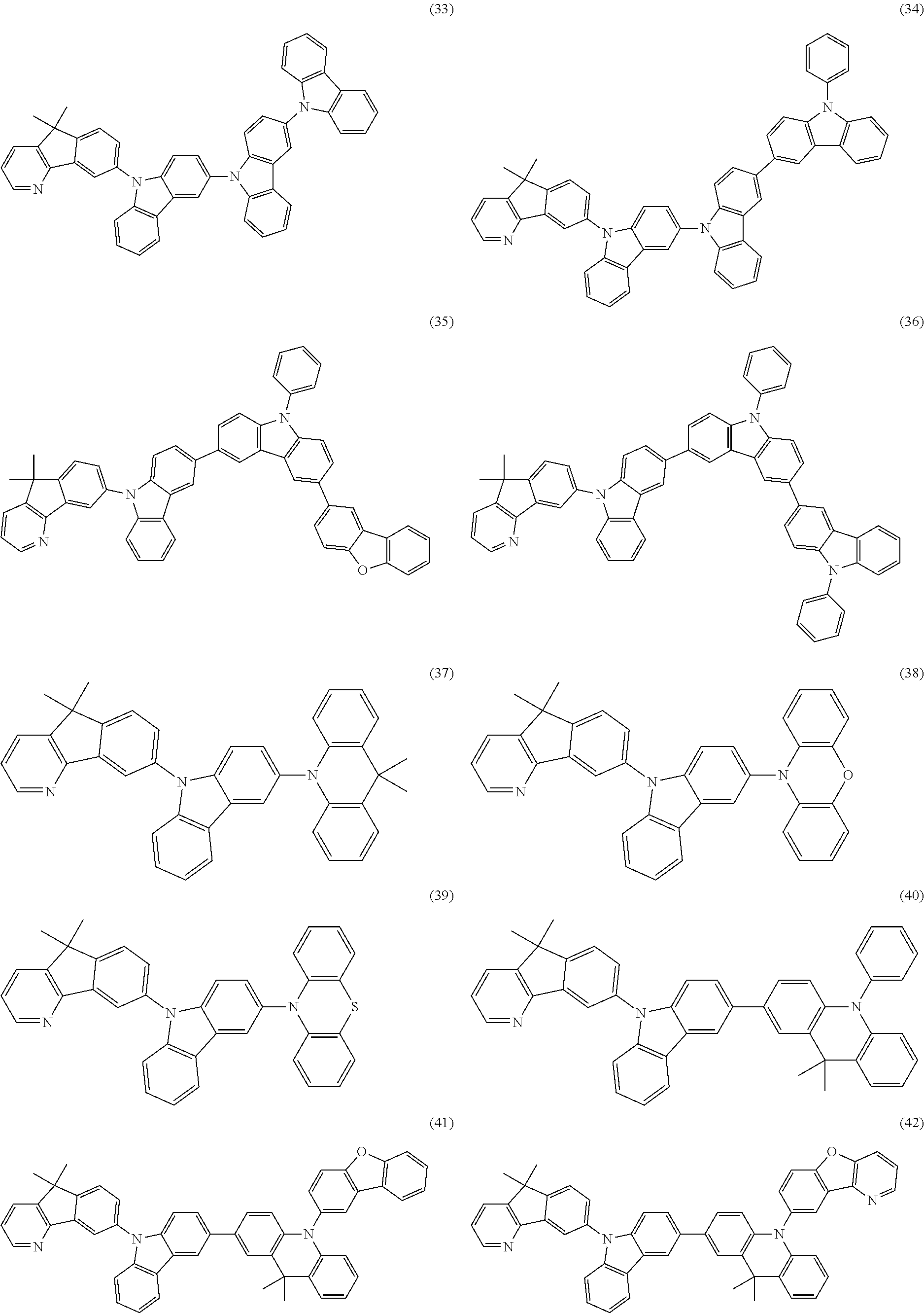


The compound represented by the formula (1) can be obtained by the following synthesis route, for example.

wherein R represents the same as R2 in the formula (1).
The material for an organic electroluminescence device (organic EL device) of the invention (hereinafter, also referred to as the material of the invention) is characterized by containing the above-mentioned compound of the invention.
The material for an organic EL device of the invention can be suitably used as a material for an organic thin film layer constituting an organic EL device.
Subsequently, the organic EL device of the invention will be explained.
The organic EL device of the invention comprises one or more organic thin film layers including an emitting layer between an anode and a cathode. The material for an organic EL device of the invention is contained in at least one of the organic thin film layers.
In the organic EL device of the invention, it is preferred that the emitting layer contain the material for an organic EL device of the invention as a host material.
It is preferred that the emitting layer contain a phosphorescent emitting material, and the phosphorescent emitting material be an ortho-metalated complex of a metal atom selected from iridium (Ir), osmium (Os), and platinum (Pt).
In addition, in the organic EL device of the invention, it is preferred that an electron-transporting region be disposed between the cathode and the emitting layer, and the electron-transporting region comprise the material for an organic EL device of the invention.
It is preferred that an electron-injecting layer be disposed between the emitting layer and the cathode, and the electron-injecting layer comprise a nitrogen-containing ring derivative.
It is preferred that a hole-transporting region be disposed between the emitting layer and the anode, and the hole-transporting region comprise the above-mentioned material for an organic electroluminescence device.
The organic EL device 1 has a construction in which an anode 20, a hole-transporting region 30, a phosphorescent emitting layer 40, an electron-transporting region 50 and a cathode 60 are stacked on a substrate 10 in this order. The hole-transporting region 30 means a hole-transporting layer, a hole-injecting layer or the like. Similarly, the electron-transporting region 50 means an electron-transporting layer, an electron-injecting layer or the like. These layers may not be formed. It is preferred that one or more of these layers be formed. In this device, each organic layer provided in the hole-transporting region 30, the phosphorescent emitting layer 40 and each organic layer provided in the electron-transporting region 50 correspond to the above-mentioned organic thin film layers. Of these organic thin film layers, at least one layer contains the material for an organic EL device of the invention. Thereby, the resulting organic EL device can be driven at a low voltage.
Meanwhile, in the organic thin film layer containing the material for an organic EL device of the invention, the content of the material is preferably 1 to 100% by weight.
In the organic EL device of the invention, the material for an organic EL device of the invention is preferably contained in the phosphorescent emitting layer 40, and in particular, is preferably used as a host material in the emitting layer. Since the material of the invention has sufficiently large triplet energy, even if a blue phosphorescent dopant material is used, the triplet energy of the phosphorescent dopant material can be efficiently confined in the emitting layer. Meanwhile, the material of the invention can be used not only in a blue emitting layer but also in an emitting layer which emits light having a longer wave length (green to red or the like).
The phosphorescent emitting layer contains a phosphorescent emitting material (phosphorescent dopant). As the phosphorescent dopant, metal complex compounds can be given. Preferable is a compound having a metal atom selected from Ir, Pt, Os, Au, Cu, Re and Ru and a ligand. The ligand preferably has an ortho-metal bond.
In respect of a high phosphorescent quantum yield and capability of improving the external quantum efficiency of an emitting device, the phosphorescent dopant is preferably a compound having a metal atom selected from Ir, Os and Pt. Further preferable are a metal complex such as an iridium complex, an osmium complex and a platinum complex. Among them, an iridium complex and a platinum complex are more preferable, and an ortho-metalated iridium complex is most preferable. The dopant may be used singly or in combination of two or more.
The concentration of the phosphorescent dopant in the phosphorescent emitting layer is, but not particularly limited to, preferably 0.1 to 30% by weight, with 0.1 to 20% by weight being more preferable.
It is also preferred that the material of the invention be used in layers adjacent to the phosphorescent emitting layer 40. For example, in the device shown in FIG. 1 , when a layer containing the material of the invention is formed between the hole-transporting region 30 and the phosphorescent emitting layer 40, (which is the layer adjacent to the emitting layer in the anode side), the layer can function as an electron-blocking layer and an exciton-barrier layer.
On the other hand, when a layer containing the material of the invention is formed between the phosphorescent emitting layer 40 and the electron-transporting region 50, (which is the layer adjacent to the emitting layer in the cathode side), the layer can function as a hole-blocking layer and an exciton-barrier layer.
Meanwhile, the blocking (barrier) layer is the layer which blocks transporting of carriers or diffusion of excitons. The organic layer which prevents electrons from leaking from an emitting layer into a hole-transporting region is mainly defined as an electron-blocking layer. The organic layer which prevents holes from leaking from an emitting layer into an electron-transporting region is often defined as a hole-blocking layer. In addition, the organic layer which prevents triplet excitons generated in an emitting layer from diffusing to the peripheral layers having lower triplet energy than that of the emitting layer is often defined as an exciton-barrier layer (triplet-blocking layer).
Moreover, it is also possible to use the material of the invention in the layers adjacent to the phosphorescent emitting layer 40, and further in other organic thin film layers which bond to the adjacent layers.
In addition, when two or more emitting layers are formed, the material of the invention can be suitably used in a spacing layer formed between the emitting layers.
The organic EL device 2 is an example of a hybrid-type organic EL device in which a phosphorescent emitting layer and a fluorescent emitting layer are stacked.
The organic EL device 2 has the same construction as the above-mentioned organic EL device 1, except that a spacing layer 42 and a fluorescent emitting layer 44 are formed between a phosphorescent emitting layer 40 and an electron-transporting region 50. In the construction in which the phosphorescent emitting layer 40 and the fluorescent emitting layer 44 are stacked, for preventing excitons generated in the phosphorescent emitting layer 40 from diffusing into the fluorescent emitting layer 44, the spacing layer 42 may be provided between the fluorescent emitting layer 44 and the phosphorescent emitting layer 40. Since the material of the invention has a large triplet energy, it can function as a spacing layer.
In the organic EL device 2, for example, by allowing the phosphorescent emitting layer to emit yellow light and by allowing the fluorescent emitting layer to emit blue light, an organic EL device which emits white light can be obtained. Meanwhile, in this embodiment, the phosphorescent emitting layer and the fluorescent emitting layer are each formed as a single layer. However, the configuration is not limited thereto, and they may be each formed as two or more layers. Their manner of formation can be selected appropriately depending on the intended use such as lightning or a display device. For example, when a full-color emitting device is realized by utilizing a white emitting device and color filters, the phosphorescent emitting layer and the fluorescent emitting layer preferably include emissions in the plural wave length regions such as red, green and blue (RGB), or red, green, blue and yellow (RGBY) in respect of color rendering properties.
In addition to the above-mentioned embodiments, the organic EL device of the invention can employ various known structures. Further, the emission from an emitting layer can be outcoupled from the anode side, the cathode side or the both sides.
In the organic EL device of the invention, the constitution of layers other than those using the above-mentioned material of an organic EL device of the invention is not particularly limited. As the constitution of the layers, known materials and the like can be used. Hereinafter, the layers of the device according to the embodiment 1 will be briefly explained. However, the materials applied to the organic EL device of the invention are not limited to the following.
(Substrate)
As the substrate, a glass plate, a polymer plate or the like can be used.
As the glass plate, particularly, soda-lime glass, barium/strontium-containing glass, lead glass, aluminosilicate glass, borosilicate glass, barium borosilicate glass, quartz or the like can be given. As the polymer plate, polycarbonate, acrylic resin, polyethylene terephthalate, polyethersulfone, polysulfone or the like can be given.
(Anode)
The anode is formed of a conductive material, for example. A conductive material having a work function larger than 4 eV is suitable.
Examples of the above-mentioned conductive material include carbon, aluminum, vanadium, iron, cobalt, nickel, tungsten, silver, gold, platinum, palladium or the like and alloys thereof, a metal oxide such as tin oxide or indium oxide used in ITO substrate or NESA substrate, and an organic conductive resin such as polythiophene and polypyrrole.
The anode can be formed in the form of two or more layers if needed.
(Cathode)
The cathode is formed of a conductive material, for example. A conductive material having a work function smaller than 4 eV is suitable.
Examples of the above-mentioned conductive material include magnesium, calcium, tin, lead, titanium, yttrium, lithium, ruthenium, manganese, aluminum, lithium fluoride or the like, and alloys thereof, but not limited thereto.
Further, representative examples of the above-mentioned alloys include magnesium/silver, magnesium/indium, lithium/aluminum, but not limited thereto. The ratio of the alloy can be selected appropriately by controlling the temperature of a deposition source, the atmosphere, the vacuum level or the like.
The cathode may be formed in the form of two or more layers if needed. The cathode can be prepared by forming a thin film of the above-mentioned conductive material by deposition, sputtering or the like.
When emission from an emitting layer is outcoupled through a cathode, it is preferred that the transmittance for emission of the cathode be larger than 10%.
In addition, the sheet resistance as a cathode is preferably several hundred Ω/□ or less. The thickness is normally 10 nm to 1 μm, with 50 to 200 nm being preferable.
(Emitting Layer)
When a phosphorescent emitting layer is formed by using materials other than the material for an organic EL device of the invention, materials which are known as a material for a phosphorescent emitting layer can be used. Specifically, reference can be made to WO2005/079118 or the like.
The organic EL device of the invention may comprise a fluorescent emitting layer as the device shown in FIG. 2 . For the fluorescent emitting layer, known materials can be used.
The emitting layer can be a double-host (often referred to as host/co-host) type. Specifically, in the emitting layer, an electron-transporting host and a hole-transporting host may be combined to control the carrier balance.
The emitting layer also can be of a double-dopant type. By incorporating two or more kinds of dopant materials having a high quantum yield to the emitting layer, each dopant emits. For example, there may be a case that a yellow emitting layer is realized by co-depositing a host, and a red dopant and a green dopant.
The emitting layer may be a single layer, or have a stacked structure. When the emitting layer has a stacked structure, due to the accumulation of electrons and holes in the interface of the emitting layers, the recombination region can be concentrated in the interface of the emitting layers, thereby increasing the quantum efficiency.
(Hole-Injecting Layer and Hole-Transporting Layer)
The hole-injecting/transporting layer helps holes to be injected to an emitting layer and transports the injected holes to an emitting region. It has a large hole mobility and normally a small ionization energy of 5.6 eV or less.
As the material for a hole-injecting/transporting layer, materials which can transport holes to an emitting layer at a lower electric field intensity are preferable. In addition, it is preferred that the hole mobility be at least 10-4 cm2/V·second when an electric field intensity of 104 to 106 V/cm is applied, for example.
Specific examples of materials for a hole-injecting/transporting layer include triazole derivatives (see U.S. Pat. No. 3,112,197 and others), oxadiazole derivatives (see U.S. Pat. No. 3,189,447 and others), imidazole derivatives (see JP-B-37-16096 and others), polyarylalkane derivatives (see U.S. Pat. Nos. 3,615,402, 3,820,989 and 3,542,544, JP-B-45-555 and 51-10983, JP-A-51-93224, 55-17105, 56-4148, 55-108667, 55-156953 and 56-36656, and others), pyrazoline derivatives and pyrazolone derivatives (see U.S. Pat. Nos. 3,180,729 and 4,278,746, JP-A-55-88064, 55-88065, 49-105537, 55-51086, 56-80051, 56-88141, 57-45545, 54-112637 and 55-74546, and others), phenylene diamine derivatives (see U.S. Pat. No. 3,615,404, JP-B-51-10105, 46-3712, 47-25336 and 54-119925, and others), arylamine derivatives (see U.S. Pat. Nos. 3,567,450, 3,240,597, 3,658,520, 4,232,103, 4,175,961 and 4,012,376, JP-B-49-35702 and 39-27577, JP-A-55-144250, 56-119132 and 56-22437, DE1,110,518, and others), amino-substituted chalcone derivatives (see U.S. Pat. No. 3,526,501, and others), oxazole derivatives (ones disclosed in U.S. Pat. No. 3,257,203, and others), styrylanthracene derivatives (see JP-A-56-46234, and others), fluorenone derivatives (JP-A-54-110837, and others), hydrazone derivatives (see U.S. Pat. No. 3,717,462, JP-A-54-59143, 55-52063, 55-52064, 55-46760, 57-11350, 57-148749 and 2-311591, and others), stilbene derivatives (see JP-A-61-210363, 61-228451, 61-14642, 61-72255, 62-47646, 62-36674, 62-10652, 62-30255, 60-93455, 60-94462, 60-174749 and 60-175052, and others), silazane derivatives (U.S. Pat. No. 4,950,950), polysilanes (JP-A-2-204996), and aniline copolymers (JP-A-2-282263).
Also, an inorganic compound such as p-type Si and p-type SiC can be used as the hole-injecting material.
As the material for a hole-injecting/transporting layer, a cross-linking material can be used. As the cross-linking hole-injecting/transporting layer, a layer formed of the cross-linking material disclosed in Chem. Mater. 2008, 20, 413-422, Chem. Mater. 2011, 23(3), 658-681, WO2008108430, WO2009102027, WO2009123269, WO2010016555, WO2010018813 or the like insolubilized by heat, light or the like can be given, for example.
(Electron-Injecting Layer and Electron-Transporting Layer)
The electron-injecting/transporting layer helps electrons to be injected to an emitting layer and transports the injected electrons to an emitting region. It has a large electron mobility.
In the organic EL device, it is known that since emitting light is reflected by an electrode (a cathode, for example), emission outcoupled directly from an anode interferes with emission after being reflected by the electrode. In order to utilize the interference effect efficiently, the film thickness of the electron injecting/transporting layer is appropriately selected to be several nm to several μm. When the film thickness is particularly large, it is preferred that the electron mobility be at least 10−5 cm2/V·s or more at an applied electric field intensity of 104 to 106 V/cm in order to avoid an increase in voltage.
As the electron-transporting material used in the electron-injecting/transporting layer, an aromatic hetero ring compound containing one or more hetero atoms in the molecule is preferably used, with a nitrogen-containing ring derivative being particularly preferable. Further, as the nitrogen-containing ring derivative, an aromatic ring having a nitrogen-containing six-membered ring or five-membered ring skeleton, or a fused aromatic ring compound having a nitrogen-containing six-membered ring or five-membered ring skeleton is preferable. Examples thereof include compounds containing a pyridine ring, a pyrimidine ring, a triazine ring, a benzimidazole ring, a phenanthroline ring, a quinazoline ring or the like in the skeleton.
In addition, an organic layer with a semiconductor property may be formed by doping a donor material (n) or doping an acceptor material (p). Representative examples of N-doping include doping of an electron-transporting material with a metal such as Li or Cs. Representative examples of P-doping include doping of a hole-transporting material with an acceptor material such as F4TCNQ (see Japan Patent No. 3695714, for example).
The organic EL device of the invention preferably comprises at least one of an electron-donating dopant and an organic metal complex in the interface region between a cathode and an organic thin film layer.
By this structure, the organic EL device can have an improved luminance and a prolonged life.
As the electron-donating dopant, at least one selected from an alkali metal, an alkali metal compound, an alkaline-earth metal, an alkaline-earth metal compound, a rare-earth metal and a rare-earth metal compound can be given.
As the organic metal complex, at least one selected from an organic metal complex including an alkali metal, an organic metal complex including an alkaline-earth metal and an organic metal complex including a rare-earth metal can be given.
As the alkali metal, lithium (Li) (work function: 2.93 eV), sodium (Na) (work function: 2.36 eV), potassium (K) (work function: 2.28 eV), rubidium (Rb) (work function: 2.16 eV), cesium (Cs) (work function: 1.95 eV) and the like can be given. One having a work function of 2.9 eV or less is particularly preferable. Of these, K, Rb and Cs are preferable, Rb or Cs is further preferable, and Cs is most preferable.
As the alkaline-earth metal, calcium (Ca) (work function: 2.9 eV), strontium (Sr) (work function: 2.0 eV or more and 2.5 eV or less), barium (Ba) (work function: 2.52 eV) and the like can be given. One having a work function of 2.9 eV or less is particularly preferable.
As the rare-earth metal, scandium (Sc), yttrium (Y), cerium (Ce), terbium (Tb), ytterbium (Yb) and the like can be given. One having a work function of 2.9 eV or less is particularly preferable.
The preferable metals of the above-mentioned metals have a particularly high reducing ability, and hence can provide the resulting organic EL device with an improved luminance and a prolonged life by adding a relative small amount of the metal to an electron-injecting region.
Examples of the alkali metal compound include an alkali oxide such as lithium oxide (Li2O), cesium oxide (Cs2O) or potassium oxide (K2O), and an alkali halide such as lithium fluoride (LiF), sodium fluoride (NaF), cesium fluoride (CsF) or potassium fluoride (KF). Of these, lithium fluoride (LiF), lithium oxide (Li2O) and sodium fluoride (NaF) are preferable.
Examples of the alkaline-earth metal compound include barium oxide (BaO), strontium oxide (SrO), calcium oxide (CaO), and mixtures thereof such as barium strontium oxide (BaxSr1-xO) (0<x<1) and barium calcium oxide (BaxCa1-xO) (0<x<1). Of these, BaO, SrO and CaO are preferred.
Examples of the rare-earth metal compound include ytterbium fluoride (YbF3), scandium fluoride (ScF3), scandium oxide (ScO3), yttrium oxide (Y2O3), cerium oxide (Ce2O3), gadolinium fluoride (GdF3) and terbium fluoride (TbF3). Of these, YbF3, ScF3 and TbF3 are preferable.
The organic metal complexes are not particularly limited as long as the complexes each contain, as a metal ion, at least one of alkali metal ions, alkaline-earth metal ions, and rare-earth metal ions, as mentioned above. Meanwhile, preferred examples of the ligand include, but are not limited to, quinolinol, benzoquinolinol, acridinol, phenanthridinol, hydroxyphenyloxazole, hydroxyphenylthiazole, hydroxydiaryloxadiazole, hydroxydiarylthiadiazole, hydroxyphenylpyridine, hydroxyphenylbenzimidazole, hydroxybenzotriazole, hydroxyfluborane, bipyridyl, phenanthroline, phthalocyanine, porphyrin, cyclopentadiene, β-diketones, azomethines, and derivatives thereof.
For the addition form of the electron-donating dopant and the organic metal complex, it is preferred that the electron-donating dopant and the organic metal complex be formed in a shape of a layer or an island in the interfacial region. A preferred method for the formation is a method in which while at least one of the electron-donating dopant and the organic metal complex is deposited by a resistant heating deposition method, an organic substance as a light emitting material or an electron-injecting material for forming the interfacial region is deposited at the same time, thereby dispersing at least one of the electron-donating dopant and the organic metal complex reducing dopant in the organic substance. The disperse concentration by molar ratio of the organic substance to the electron-donating dopant and/or the organic metal complex is normally 100:1 to 1:100, preferably 5:1 to 1:5.
In a case where at least one of the electron-donating dopant and the organic metal complex is formed into the shape of a layer, the light emitting material or electron injecting material which serves as an organic layer in the interface is formed into the shape of a layer. After that, at least one of the electron-donating dopant and the organic metal complex is solely deposited by the resistant heating deposition method to form a layer preferably having a thickness of 0.1 nm or more and 15 nm or less.
In a case where at least one of the electron-donating dopant and the organic metal complex is formed into the shape of an island, the light emitting material or the electron injecting material which serves as an organic layer in the interface is formed into the shape of an island. After that, at least one of the electron-donating dopant and the organic metal complex is solely deposited by the resistant heating deposition method to form an island preferably having a thickness of 0.05 nm or more and 1 nm or less.
In addition, the ratio of the main component (the emitting material or the electron-injecting material) to at least one of the electron-donating dopant and the organic metal complex in the organic EL device of the invention is preferably 5:1 to 1:5, more preferably 2:1 to 1:2 in terms of a molar ratio.
Each layer of the organic EL device of the invention can be formed by using known methods including the dry-type film formation such as vacuum deposition, sputtering, plasma ion-plating or the like and the wet-type film formation such as spin coating, dipping, flow coating or the like.
The film thickness of each layer is not particularly limited, but is required to be set to be a proper thickness. If the film thickness is too large, a large applied voltage is required in order to obtain the predetermined light output, thereby leading to low efficiency. If the film thickness is too small, due to generation of pinholes or the like, sufficient luminance cannot be obtained when an electric field is applied. Normally, the film thickness is preferably 5 nm to 10 μm, and the range of 10 nm to 0.2 μm is further preferable.
The following compound (1) was synthesized.

- (1) Synthesis of Intermediate (1-a)

Under a nitrogen atmosphere, 15.20 g (100 mmol) of 3-methoxyphenyl boronic acid, 18.56 g (100 mmol) of ethyl 2-chloro nicotinate, 2.31 g (2.00 mmol) of tetrakis(triphenylphosphine)palladium, 150 mL of 1,4-dioxane and 150 mL of a 2M aqueous solution of potassium carbonate were placed in a three neck flask, and refluxed for 8 hours. After completion of the reaction, the resulting mixture was cooled to room temperature, and then subjected to extraction with dichloromethane by means of a separating funnel and dried with anhydrous magnesium sulfate, followed by filtration and concentration. The crude product obtained was purified by a using silica gel column to obtain a yellow oily matter (intermediate (1-a)). The yield was 25.72 g and the percent yield was 100%.
- (2) Synthesis of Intermediate (1-b)

Under a nitrogen atmosphere, 25.72 g (100 mmol) of intermediate (1-a) and 120 mL of dehydrated tetrahydrofuran were placed in a three neck flask, and cooled to −78° C. To the resulting solution, 263.2 mL (1.14M in diethylether, 300 mmol) of methyllithium was added dropwise for 10 minutes. After stirred at −78° C. for 20 minutes, the resulting mixture was heated to room temperature, and then stirred at room temperature for 24 hours. After completion of the reaction, 50 mL of water was added. The mixture was subjected to extraction with ethyl acetate by using a separating funnel, and dried with anhydrous magnesium sulfate, followed by filtration and concentration. The crude product obtained was purified by using a silica gel column to obtain yellow solids (intermediate (1-b)). The yield was 14.81 g and the percent yield was 61%.
- (3) Synthesis of Intermediate (1-c)

Under a nitrogen atmosphere, 13.60 g (55.9 mmol) of intermediate (1-b) and 100 g of polyphosphoric acid were placed in a three neck flask, and stirred at 70° C. for 48 hours. After a completion of the reaction, the mixture was cooled to room temperature and ice was added. The mixture was neutralized in a saturated aqueous solution of sodium hydrocarbon. The resulting solution was subjected to extraction with dichloromethane by using a separating funnel and dried with anhydrous magnesium sulfate, followed by filtration and concentration. The crude product obtained was purified by using a silica gel column to obtain an oily yellow matter (intermediate (1-c)). The yield was 7.34 g and the percent yield was 58%.
- (4) Synthesis of Intermediate (1-d)

Under a nitrogen atmosphere, 7.34 g (32.6 mmol) of intermediate (1-c) and 160 mL of dichloromethane were placed in a three neck flask, and cooled to 0° C. To the resulting solution, 32.6 mL (1M in dichloromethane, 32.6 mmol) of boron tribromide was added dropwise for 10 minutes. After stirred at 0° C. for 20 minutes, the resulting mixture was heated to room temperature, and then stirred at room temperature for 19 hours. After a completion of the reaction, the resultant was cooled to 0° C., and 50 mL of water was added. The mixture was subjected to extraction with dichloromethane by using a separating funnel, and dried with anhydrous magnesium sulfate, followed by filtration and concentration. The crude product obtained was purified by using a silica gel column to obtain white solids (intermediate (1-d)). The yield was 6.20 g and the percent yield was 90%.
- (5) Synthesis of Intermediate (1-e)

Under a nitrogen atmosphere, 6.20 g (29.3 mmol) of intermediate (1-d), 4.64 g (58.6 mmol) of pyridine and 80 mL of dichloromethane were placed in a three neck flask, and cooled to 0° C. To the resulting solution, 5.92 mL of trifluoromethanesulfonic anhydride was added dropwise for 10 minutes. After stirred at 0° C. for 20 minutes, the resulting mixture was heated to room temperature, and then stirred at room temperature for 8 hours. After completion of the reaction, the resulting solution was cooled to 0° C., followed by addition of 50 mL of 10% hydrochloric acid. The mixture was subjected to extraction with dichloromethane by using a separating funnel. The extracted matter was washed with a saturated aqueous solution of sodium hydrogen carbonate, and dried with anhydrous magnesium sulfate, followed by filtration and concentration. The crude product obtained was purified by using silica gel column to obtain white solids (intermediate (1-e)). The yield was 9.10 g and the percent yield was 89%.
- (6) Synthesis of Compound (1)

Under a nitrogen atmosphere, 8.82 g (25.7 mmol) of intermediate (1-e), 3.41 g (10.3 mmol) of 3,3′-bis(9H-carbazole), 0.23 g (1.03 mmol) of palladium acetate, 1.09 g (2.57 mmol) of 2-di-t-butylphosphino-2′,4′,6′-triisopropyl biphenyl, 10.90 g (51.4 mmol) of potassium phosphate, 0.13 g (1.03 mmol) of phenylboronic acid, 20 mL of toluene and 40 mL of t-butanol were placed in a three neck flask, and refluxed at 110° C. for 15 hours. After completion of the reaction, the resulting mixture was cooled to room temperature, and then subjected to extraction with dichloromethane by means of a separating funnel and dried with anhydrous magnesium sulfate, followed by filtration and concentration. The crude product obtained was purified by using a silica gel column to obtain white solids (compound (1)) (yield: 4.80 g, percent yield: 65%). By field desorption mass spectrometry, the white solids obtained was identified to compound (1).
A glass substrate with ITO electrode lines having a film thickness of 130 nm (manufactured by Geomatics Co.) was subjected to ultrasonic cleaning in isopropyl alcohol for 5 minutes and then UV ozone cleaning for 30 minutes.
The cleaned glass substrate with transparent electrode lines was mounted on a substrate holder in a vacuum deposition apparatus. The following compound (HI1) was deposited by resistance heating on the surface of the glass substrate on which the transparent electrode lines had been formed such that the ITO electrode lines were covered to form a 20 nm-thick film, and subsequently the following compound (HT1) to form a 60 nm-thick film. The films were formed at a deposition rate of 1 Å/s. These thin films served as a hole-injecting layer and a hole-transporting layer, respectively.
Next, on the hole-transporting layer, the following compound (H1) and the following compound (BD1) were simultaneously deposited by resistance heating to form a 50 nm-thick film. Then compound (BD1) was deposited such that the mass ratio of compound (BD1) relative to the total mass of compound (H1) and compound (BD1) become 20%. The film formation rates were set to be 1.2 Å/s and 0.3 Å/s, respectively. This thin film served as a phosphorescent emitting layer.
Next, on the phosphorescent emitting layer, the compound (1) obtained in synthesis example 1 was deposited by resistance heating to form a 10 nm-thick thin film. The film formation rate was 1.2 Å/s. This thin film served as a blocking layer.
Subsequently, on the blocking layer, the following compound (ET1) was deposited by resistance heating to form a 10 nm-thick thin film. The film formation rate was 1 Å/s. This thin film served as an electron-injecting layer.
Next, on the electron-injecting layer, LiF was deposited at a film formation rate of 0.1 Å/s to form a 1.0 nm-thick thin film.
Subsequently, on this LiF film, metal aluminum was deposited at a film formation rate of 8.0 Å/s to form a 80 nm-thick metal electrode, whereby an organic EL device was obtained.

The organic EL device produced was evaluated for the following items. Table 1 shows the results.
- (1) External Quantum Efficiency (%)
At 23° C., under dried nitrogen gas atmosphere, the external quantum efficiency at a luminance of 1000 cd/m2 was measured by using a luminous meter (spectral radiance meter CS-1000 manufactured by Konica Minolta, Inc.).
- (2) Half Life (Hours)
A continuous current (direct current) test was conducted at an initial luminance of 1000 cd/m2. The time taken for the luminance to decrease by half was determined.
- (3) Voltage (V)
At 23° C., under dried nitrogen gas atmosphere, using KEITHLY 236 SOURCE MEASURE UNIT, a voltage was applied to a device which has been electrically-wired, thereby to allow the device to emit. The voltage applied to the wiring resistance other the device was deducted from the entire applied voltage, whereby the voltage applied to the device was determined. At the same time of applying voltage and measurement, luminous measurement was conducted by using a luminous meter (spectral radiance meter CS-1000 manufactured by Konica Minolta, Inc.). From these measurement results, the voltage at a device luminance of 100 cd/m2 was read.
| TABLE 1 | |||||
| External | Luminance | ||||
| quantum | Half life | ||||
| Blocking layer | Voltage (V) | efficiency (%) | (hours) | ||
| Example 1 | Compound (1) | 4.8 | 17.5 | 7300 |
Table 2 shows the triplet energies of the materials for an organic EL device used in Examples. The triplet energy is defined as follows. A sample is dissolved in an EPA solvent (diethyl ether: isopentane: ethanol=5:5:2 (volume ratio)) at the ratio of 10 μmol/L to obtain a sample for phosphorescent measurement. The sample for phosphorescent measurement is put in a quartz cell. The quartz cell is irradiated with excited light at a temperature of 77K. The radiated phosphorescent spectrum is measured. The triplet energy is determined from the measured spectrum by converting with the expression: Et(ev)=1239.85/λedge.
| TABLE 2 | |||
| Compound | Triplet energy (eV) | ||
| Compound (1) | 2.91 | ||
| Compound (BD1) | 2.64 | ||
From Table 1, it is found that the organic EL device using the material for an organic EL device of the invention has a long life, a high efficiency, and can be driven at a low voltage.
Moreover, from Table 2, it is found that the material for an organic EL device of the invention has a high triplet energy, which can be used as a blocking layer material for a blue phosphorescence-emitting EL device.
The organic EL device of the invention can be utilized for a planar emitting body such as a flat panel display of a wall-hanging television, a copier, a printer, a back light of a liquid crystal display, or a light source in instruments or the like, a sign board, a signal light or the like.
The material for an organic EL device of the invention can be used for an organic EL device, an organic EL display, lightnings, an organic semiconductor, an organic solar cell or the like.
The material for an organic EL device of the invention is useful for realizing an organic EL device which can be driven at a low voltage with a high efficiency and a prolonged life.
Although only some exemplary embodiments and/or examples of this invention have been described in detail above, those skilled in the art will readily appreciate that many modifications are possible in the exemplary embodiments and/or examples without materially departing from the novel teachings and advantages of this invention. Accordingly, all such modifications are intended to be included within the scope of this invention.
The documents described in this specification and the Japanese application specification claiming priority under the Paris Convention are incorporated herein by reference in its entirety.
Claims (16)
1. A compound represented by the following formula (1):

wherein X1 to X7 are independently a nitrogen atom, or a carbon atom that R1 is bonded to, provided that at least one of X1 to X7 is a nitrogen atom;
R1 represents a hydrogen atom, a substituted or unsubstituted alkyl group including 1 to 20 carbon atoms, a substituted or unsubstituted cycloalkyl group including 3 to 18 ring carbon atoms, a substituted or unsubstituted alkoxy group including 1 to 20 carbon atoms, a substituted or unsubstituted cycloalkoxy group including 3 to 18 ring carbon atoms, a substituted or unsubstituted silyl group, or a fluoro group, and when two or more R1s are present in the formula (1), R1s may be the same or different from each other;
X8 to X15 are independently a nitrogen atom, or a carbon atom that R2 is bonded to;
R2 represents a hydrogen atom, a substituted or unsubstituted alkyl group including 1 to 20 carbon atoms, a substituted or unsubstituted cycloalkyl group including 3 to 18 ring carbon atoms, a substituted or unsubstituted alkoxy group including 1 to 20 carbon atoms, a substituted or unsubstituted cycloalkoxy group including 3 to 18 ring carbon atoms, a substituted or unsubstituted aryl group including 6 to 18 ring carbon atoms, a substituted or unsubstituted aryloxy group including 6 to 18 ring carbon atoms, a substituted or unsubstituted heteroaryl group including 5 to 18 ring atoms, a substituted or unsubstituted amino group, a substituted or unsubstituted silyl group, a fluoro group, or a cyano group, and when two or more R2s are present in the formula (1), R2s may be the same or different from each other; and
A1 and A2 are independently a substituted or unsubstituted alkyl group including 1 to 20 carbon atoms, a substituted or unsubstituted cycloalkyl group including 3 to 18 ring carbon atoms, a substituted or unsubstituted alkoxy group including 1 to 20 carbon atoms, a substituted or unsubstituted cycloalkoxy group including 3 to 18 ring carbon atoms, a substituted or unsubstituted aryl group including 6 to 18 ring carbon atoms, a substituted or unsubstituted aryloxy group including 6 to 18 ring carbon atoms, a substituted or unsubstituted heteroaryl group including 5 to 18 ring atoms, a substituted or unsubstituted amino group, a substituted or unsubstituted silyl group, a fluoro group, or a cyano group.
2. The compound according to claim 1 , which is a compound represented by the following formula (2):

wherein X1 to X15, A1 and A2 independently represent the same as in the formula (1);
X16 to X23 are independently a nitrogen atom, or a carbon atom that R3 is bonded to;
R3 represents a hydrogen atom, a substituted or unsubstituted alkyl group including 1 to 20 carbon atoms, a substituted or unsubstituted cycloalkyl group including 3 to 18 ring carbon atoms, a substituted or unsubstituted alkoxy group including 1 to 20 carbon atoms, a substituted or unsubstituted cycloalkoxy group including 3 to 18 ring carbon atoms, a substituted or unsubstituted aryl group including 6 to 18 ring carbon atoms, a substituted or unsubstituted aryloxy group including 6 to 18 ring carbon atoms, a substituted or unsubstituted heteroaryl group including 5 to 18 ring atoms, a substituted or unsubstituted amino group, a substituted or unsubstituted silyl group, a fluoro group, or a cyano group, and when two or more R3s are present in the formula (2), R3s may be the same or different from each other;
Y represents an oxygen atom (O), a sulfur atom (S) or NR4;
R4 represents a substituted or unsubstituted alkyl group including 1 to 20 carbon atoms, a substituted or unsubstituted cycloalkyl group including 3 to 18 ring carbon atoms, a substituted or unsubstituted alkoxy group including 1 to 20 carbon atoms, a substituted or unsubstituted cycloalkoxy group including 3 to 18 ring carbon atoms, a substituted or unsubstituted aryl group including 6 to 18 ring carbon atoms, a substituted or unsubstituted aryloxy group including 6 to 18 ring carbon atoms, a substituted or unsubstituted heteroaryl group including 5 to 18 ring atoms, a substituted or unsubstituted amino group, a substituted or unsubstituted silyl group, a fluoro group, or a cyano group;
W represents a single bond, O, S, P(R5), P(═O)(R6), N(R7), Si(R8)(R9) or C(R10)(R11); and
R5 to R11 independently represent a substituted or unsubstituted alkyl group including 1 to 20 carbon atoms, a substituted or unsubstituted cycloalkyl group including 3 to 18 ring carbon atoms, a substituted or unsubstituted alkoxy group including 1 to 20 carbon atoms, a substituted or unsubstituted cycloalkoxy group including 3 to 18 ring carbon atoms, a substituted or unsubstituted aryl group including 6 to 18 ring carbon atoms, a substituted or unsubstituted aryloxy group including 6 to 18 ring carbon atoms, a substituted or unsubstituted heteroaryl group including 5 to 18 ring atoms, a substituted or unsubstituted amino group, a substituted or unsubstituted silyl group, a fluoro group, or a cyano group, provided that one carbon atom selected from X12 to X15 is bonded through a single bond to one carbon atom selected from X16 to X19 or a nitrogen atom when Y is NR4.
3. The compound according to claim 2 , which is a compound represented by the following formula (3):

wherein X1 to X23, A1, A2 and Y independently represent the same as in the formula (2).
4. The compound according to claim 2 , which is a compound represented by the following formula (4):

wherein X1 to X12, X14 to X17, X19 to X23, A1, A2 and Y independently represent the same as in the formula (2).
5. The compound according to claim 2 , which is a compound represented by the following formula (5):

wherein X1 to X12, X14 to X17, X19 to X23, Al and A2 independently represent the same as in the formula (2); and
A3 represents a substituted or unsubstituted alkyl group including 1 to 20 carbon atoms, a substituted or unsubstituted cycloalkyl group including 3 to 18 ring carbon atoms, a substituted or unsubstituted alkoxy group including 1 to 20 carbon atoms, a substituted or unsubstituted cycloalkoxy group including 3 to 18 ring carbon atoms, a substituted or unsubstituted aryl group including 6 to 18 ring carbon atoms, a substituted or unsubstituted aryloxy group including 6 to 18 ring carbon atoms, a substituted or unsubstituted heteroaryl group including 5 to 18 ring atoms, a substituted or unsubstituted amino group, a substituted or unsubstituted silyl group, a fluoro group, or a cyano group.
6. The compound according to claim 2 , which is a compound represented by the following formula (6):

wherein X1 to X12, X14 to X23, A1 and A2 independently represent the same as in the formula (2).
7. The compound according to claim 1 , wherein at least one of X1 to X4 and X7 is N.
8. A material for an organic electroluminescence device comprising the compound according to claim 1 .
9. An organic electroluminescence device comprising one or more organic thin film layers including an emitting layer between a cathode and an anode, wherein at least one layer of the organic thin film layers comprises the material for an organic electroluminescence device according to claim 8 .
10. The organic electroluminescence device according to claim 9 , wherein the organic emitting layer comprises the material for an organic electroluminescence device.
11. The organic electroluminescence device according to claim 9 , wherein the organic emitting layer comprises a phosphorescent material, the phosphorescent material being an ortho-metalated complex of a metal atom selected from iridium (Ir), osmium (Os) and platinum (Pt).
12. The organic electroluminescence device according to claim 9 , which comprises an electron-transporting region between the cathode and the emitting layer, the electron-transporting region comprising the material for an organic electroluminescence device.
13. The electroluminescence device according to claim 9 , which comprises an electron-injecting layer between the organic emitting layer and the cathode, the electron-injecting layer comprising a nitrogen-containing ring derivative.
14. The compound according to claim 2 , wherein at least one of X1 to X4 and X7 is N.
15. The compound according to claim 4 , wherein at least one of X1 to X4 and X7 is N.
16. The compound according to claim 6 , wherein at least one of X1 to X4 and X7 is N.
Applications Claiming Priority (3)
| Application Number | Priority Date | Filing Date | Title |
|---|---|---|---|
| JP2011-268228 | 2011-12-07 | ||
| JP2011268228 | 2011-12-07 | ||
| PCT/JP2012/007789 WO2013084484A1 (en) | 2011-12-07 | 2012-12-05 | Material for organic electroluminescent element and organic electroluminescent element using same |
Publications (2)
| Publication Number | Publication Date |
|---|---|
| US20140353650A1 US20140353650A1 (en) | 2014-12-04 |
| US9496508B2 true US9496508B2 (en) | 2016-11-15 |
Family
ID=48573874
Family Applications (1)
| Application Number | Title | Priority Date | Filing Date |
|---|---|---|---|
| US14/363,761 Active 2034-01-23 US9496508B2 (en) | 2011-12-07 | 2012-12-05 | Material for organic electroluminescent element and organic electroluminescent element using same |
Country Status (3)
| Country | Link |
|---|---|
| US (1) | US9496508B2 (en) |
| TW (1) | TW201336836A (en) |
| WO (1) | WO2013084484A1 (en) |
Families Citing this family (2)
| Publication number | Priority date | Publication date | Assignee | Title |
|---|---|---|---|---|
| WO2014084612A1 (en) * | 2012-11-30 | 2014-06-05 | 주식회사 엘지화학 | Novel compound and organic electronic element using same |
| KR101812581B1 (en) * | 2013-10-11 | 2017-12-27 | 제일모직 주식회사 | Organic alloy for organic optoelectric device and organic optoelectric device and display device |
Citations (6)
| Publication number | Priority date | Publication date | Assignee | Title |
|---|---|---|---|---|
| JP2006131783A (en) | 2004-11-08 | 2006-05-25 | Konica Minolta Holdings Inc | Material for organic electroluminescent element, organic electroluminescent element, lighting apparatus and display |
| JP2010114180A (en) * | 2008-11-05 | 2010-05-20 | Konica Minolta Holdings Inc | Organic electroluminescent element, white organic electroluminescent element, display device and illuminator |
| JP2011054931A (en) | 2009-08-05 | 2011-03-17 | Konica Minolta Holdings Inc | Organic electroluminescent element and method of manufacturing the same |
| WO2011055934A2 (en) | 2009-11-03 | 2011-05-12 | 제일모직 주식회사 | Compound for an organic photoelectric device, and organic photoelectric device comprising same |
| KR20120072787A (en) * | 2010-12-24 | 2012-07-04 | 에스에프씨 주식회사 | Pyridine derivative compound and organic electroluminescent devices comprising the same |
| KR20120092908A (en) | 2011-02-14 | 2012-08-22 | 에스에프씨 주식회사 | Pyridine derivative compound and organic electroluminescent device comprising the same |
-
2012
- 2012-12-05 WO PCT/JP2012/007789 patent/WO2013084484A1/en active Application Filing
- 2012-12-05 US US14/363,761 patent/US9496508B2/en active Active
- 2012-12-07 TW TW101146043A patent/TW201336836A/en unknown
Patent Citations (7)
| Publication number | Priority date | Publication date | Assignee | Title |
|---|---|---|---|---|
| JP2006131783A (en) | 2004-11-08 | 2006-05-25 | Konica Minolta Holdings Inc | Material for organic electroluminescent element, organic electroluminescent element, lighting apparatus and display |
| JP2010114180A (en) * | 2008-11-05 | 2010-05-20 | Konica Minolta Holdings Inc | Organic electroluminescent element, white organic electroluminescent element, display device and illuminator |
| JP2011054931A (en) | 2009-08-05 | 2011-03-17 | Konica Minolta Holdings Inc | Organic electroluminescent element and method of manufacturing the same |
| WO2011055934A2 (en) | 2009-11-03 | 2011-05-12 | 제일모직 주식회사 | Compound for an organic photoelectric device, and organic photoelectric device comprising same |
| EP2497811A2 (en) | 2009-11-03 | 2012-09-12 | Cheil Industries Inc. | Compound for an organic photoelectric device, and organic photoelectric device comprising same |
| KR20120072787A (en) * | 2010-12-24 | 2012-07-04 | 에스에프씨 주식회사 | Pyridine derivative compound and organic electroluminescent devices comprising the same |
| KR20120092908A (en) | 2011-02-14 | 2012-08-22 | 에스에프씨 주식회사 | Pyridine derivative compound and organic electroluminescent device comprising the same |
Non-Patent Citations (5)
| Title |
|---|
| International Search Report issue in International Application No. PCT/JP2012/007789 dated Feb. 19, 2013. |
| Min-Gi Shin et al., Organic Electronics 12 (2011), p. 785-793. |
| Seyhan, S., et al, Theoretical Investigation of Triscarbazole Derivatives as Host Materials for Blue Electrophosphorescence: Effects of Topology, Chemistry of Materials, Nov. 7, 2011, vol. 23, Issue 23, pp. 5223-5230. |
| Written Opinion of the International Searching Authority issued in International Application No. PCT/JP2012/007789 dated Jun. 19, 2014. |
| Xin, G., et al, Bipolar Host Molecules for Efficient Blue Electrophosphorescence: A Quantum Chemical Design, Journal of Physical Chemistry A, 2010, vol. 114, Issue 2, pp. 965-972. |
Also Published As
| Publication number | Publication date |
|---|---|
| TW201336836A (en) | 2013-09-16 |
| US20140353650A1 (en) | 2014-12-04 |
| WO2013084484A1 (en) | 2013-06-13 |
Similar Documents
| Publication | Publication Date | Title |
|---|---|---|
| US9991447B2 (en) | Material for organic electroluminescent element, and organic electroluminescent element produced using same | |
| US9685614B2 (en) | Material for organic electroluminescent element, and element using same | |
| KR102048688B1 (en) | Nitrogen-containing heteroaromatic ring compound | |
| US9960364B2 (en) | Ladder compound, and organic electroluminescent element using same | |
| WO2013175747A1 (en) | Organic electroluminescent element | |
| WO2013035329A1 (en) | Organic electroluminescence element | |
| WO2011046182A1 (en) | Fluorene-containing aromatic compound, material for organic electroluminescent element, and organic electroluminescent element using same | |
| WO2013102992A1 (en) | Material for organic electroluminescence element and element using same | |
| US20150034927A1 (en) | Material for organic electroluminescent element, and organic electroluminescent element using same | |
| WO2013175746A1 (en) | Organic electroluminescent element | |
| WO2013069242A1 (en) | Material for organic electroluminescent elements, and organic electroluminescent element using same | |
| WO2013179645A1 (en) | Organic-electroluminescent-element material, and organic electroluminescent element using same | |
| JP2013108015A (en) | Material for organic electroluminescent element | |
| WO2013108589A1 (en) | Novel compound, material for organic electroluminescent element and organic electroluminescent element | |
| JP6031302B2 (en) | Heteroaromatic compound and organic electroluminescence device using the same | |
| US9496508B2 (en) | Material for organic electroluminescent element and organic electroluminescent element using same | |
| WO2014112359A1 (en) | Organic electroluminescent element |
Legal Events
| Date | Code | Title | Description |
|---|---|---|---|
| AS | Assignment |
Owner name: IDEMITSU KOSAN CO., LTD., JAPAN Free format text: ASSIGNMENT OF ASSIGNORS INTEREST;ASSIGNORS:SHIOMI, TAKUSHI;HASHIMOTO, RYOHEI;NAGASHIMA, HIDEAKI;SIGNING DATES FROM 20140421 TO 20140423;REEL/FRAME:033051/0821 |
|
| STCF | Information on status: patent grant |
Free format text: PATENTED CASE |
|
| CC | Certificate of correction | ||
| MAFP | Maintenance fee payment |
Free format text: PAYMENT OF MAINTENANCE FEE, 4TH YEAR, LARGE ENTITY (ORIGINAL EVENT CODE: M1551); ENTITY STATUS OF PATENT OWNER: LARGE ENTITY Year of fee payment: 4 |