WO2014054570A1 - 基板処理方法、コンピュータ記憶媒体及び基板処理システム - Google Patents
基板処理方法、コンピュータ記憶媒体及び基板処理システム Download PDFInfo
- Publication number
- WO2014054570A1 WO2014054570A1 PCT/JP2013/076511 JP2013076511W WO2014054570A1 WO 2014054570 A1 WO2014054570 A1 WO 2014054570A1 JP 2013076511 W JP2013076511 W JP 2013076511W WO 2014054570 A1 WO2014054570 A1 WO 2014054570A1
- Authority
- WO
- WIPO (PCT)
- Prior art keywords
- substrate
- polymer
- block copolymer
- wafer
- mounting table
- Prior art date
- Legal status (The legal status is an assumption and is not a legal conclusion. Google has not performed a legal analysis and makes no representation as to the accuracy of the status listed.)
- Ceased
Links
Images


Classifications
-
- G—PHYSICS
- G03—PHOTOGRAPHY; CINEMATOGRAPHY; ANALOGOUS TECHNIQUES USING WAVES OTHER THAN OPTICAL WAVES; ELECTROGRAPHY; HOLOGRAPHY
- G03F—PHOTOMECHANICAL PRODUCTION OF TEXTURED OR PATTERNED SURFACES, e.g. FOR PRINTING, FOR PROCESSING OF SEMICONDUCTOR DEVICES; MATERIALS THEREFOR; ORIGINALS THEREFOR; APPARATUS SPECIALLY ADAPTED THEREFOR
- G03F7/00—Photomechanical, e.g. photolithographic, production of textured or patterned surfaces, e.g. printing surfaces; Materials therefor, e.g. comprising photoresists; Apparatus specially adapted therefor
- G03F7/0002—Lithographic processes using patterning methods other than those involving the exposure to radiation, e.g. by stamping
-
- H—ELECTRICITY
- H01—ELECTRIC ELEMENTS
- H01L—SEMICONDUCTOR DEVICES NOT COVERED BY CLASS H10
- H01L21/00—Processes or apparatus adapted for the manufacture or treatment of semiconductor or solid state devices or of parts thereof
- H01L21/67—Apparatus specially adapted for handling semiconductor or electric solid state devices during manufacture or treatment thereof; Apparatus specially adapted for handling wafers during manufacture or treatment of semiconductor or electric solid state devices or components ; Apparatus not specifically provided for elsewhere
- H01L21/67005—Apparatus not specifically provided for elsewhere
- H01L21/67011—Apparatus for manufacture or treatment
- H01L21/67098—Apparatus for thermal treatment
-
- B—PERFORMING OPERATIONS; TRANSPORTING
- B05—SPRAYING OR ATOMISING IN GENERAL; APPLYING FLUENT MATERIALS TO SURFACES, IN GENERAL
- B05C—APPARATUS FOR APPLYING FLUENT MATERIALS TO SURFACES, IN GENERAL
- B05C11/00—Component parts, details or accessories not specifically provided for in groups B05C1/00 - B05C9/00
- B05C11/02—Apparatus for spreading or distributing liquids or other fluent materials already applied to a surface ; Controlling means therefor; Control of the thickness of a coating by spreading or distributing liquids or other fluent materials already applied to the coated surface
- B05C11/08—Spreading liquid or other fluent material by manipulating the work, e.g. tilting
-
- B—PERFORMING OPERATIONS; TRANSPORTING
- B05—SPRAYING OR ATOMISING IN GENERAL; APPLYING FLUENT MATERIALS TO SURFACES, IN GENERAL
- B05C—APPARATUS FOR APPLYING FLUENT MATERIALS TO SURFACES, IN GENERAL
- B05C9/00—Apparatus or plant for applying liquid or other fluent material to surfaces by means not covered by any preceding group, or in which the means of applying the liquid or other fluent material is not important
- B05C9/08—Apparatus or plant for applying liquid or other fluent material to surfaces by means not covered by any preceding group, or in which the means of applying the liquid or other fluent material is not important for applying liquid or other fluent material and performing an auxiliary operation
- B05C9/14—Apparatus or plant for applying liquid or other fluent material to surfaces by means not covered by any preceding group, or in which the means of applying the liquid or other fluent material is not important for applying liquid or other fluent material and performing an auxiliary operation the auxiliary operation involving heating or cooling
-
- H—ELECTRICITY
- H01—ELECTRIC ELEMENTS
- H01J—ELECTRIC DISCHARGE TUBES OR DISCHARGE LAMPS
- H01J37/00—Discharge tubes with provision for introducing objects or material to be exposed to the discharge, e.g. for the purpose of examination or processing thereof
- H01J37/32—Gas-filled discharge tubes
- H01J37/32431—Constructional details of the reactor
- H01J37/32798—Further details of plasma apparatus not provided for in groups H01J37/3244 - H01J37/32788; special provisions for cleaning or maintenance of the apparatus
- H01J37/32889—Connection or combination with other apparatus
-
- H—ELECTRICITY
- H01—ELECTRIC ELEMENTS
- H01L—SEMICONDUCTOR DEVICES NOT COVERED BY CLASS H10
- H01L21/00—Processes or apparatus adapted for the manufacture or treatment of semiconductor or solid state devices or of parts thereof
- H01L21/02—Manufacture or treatment of semiconductor devices or of parts thereof
- H01L21/027—Making masks on semiconductor bodies for further photolithographic processing not provided for in group H01L21/18 or H01L21/34
- H01L21/0271—Making masks on semiconductor bodies for further photolithographic processing not provided for in group H01L21/18 or H01L21/34 comprising organic layers
-
- H—ELECTRICITY
- H01—ELECTRIC ELEMENTS
- H01L—SEMICONDUCTOR DEVICES NOT COVERED BY CLASS H10
- H01L21/00—Processes or apparatus adapted for the manufacture or treatment of semiconductor or solid state devices or of parts thereof
- H01L21/02—Manufacture or treatment of semiconductor devices or of parts thereof
- H01L21/04—Manufacture or treatment of semiconductor devices or of parts thereof the devices having potential barriers, e.g. a PN junction, depletion layer or carrier concentration layer
- H01L21/18—Manufacture or treatment of semiconductor devices or of parts thereof the devices having potential barriers, e.g. a PN junction, depletion layer or carrier concentration layer the devices having semiconductor bodies comprising elements of Group IV of the Periodic Table or AIIIBV compounds with or without impurities, e.g. doping materials
- H01L21/30—Treatment of semiconductor bodies using processes or apparatus not provided for in groups H01L21/20 - H01L21/26
- H01L21/31—Treatment of semiconductor bodies using processes or apparatus not provided for in groups H01L21/20 - H01L21/26 to form insulating layers thereon, e.g. for masking or by using photolithographic techniques; After treatment of these layers; Selection of materials for these layers
- H01L21/3105—After-treatment
- H01L21/31058—After-treatment of organic layers
-
- H—ELECTRICITY
- H01—ELECTRIC ELEMENTS
- H01L—SEMICONDUCTOR DEVICES NOT COVERED BY CLASS H10
- H01L21/00—Processes or apparatus adapted for the manufacture or treatment of semiconductor or solid state devices or of parts thereof
- H01L21/02—Manufacture or treatment of semiconductor devices or of parts thereof
- H01L21/04—Manufacture or treatment of semiconductor devices or of parts thereof the devices having potential barriers, e.g. a PN junction, depletion layer or carrier concentration layer
- H01L21/18—Manufacture or treatment of semiconductor devices or of parts thereof the devices having potential barriers, e.g. a PN junction, depletion layer or carrier concentration layer the devices having semiconductor bodies comprising elements of Group IV of the Periodic Table or AIIIBV compounds with or without impurities, e.g. doping materials
- H01L21/30—Treatment of semiconductor bodies using processes or apparatus not provided for in groups H01L21/20 - H01L21/26
- H01L21/31—Treatment of semiconductor bodies using processes or apparatus not provided for in groups H01L21/20 - H01L21/26 to form insulating layers thereon, e.g. for masking or by using photolithographic techniques; After treatment of these layers; Selection of materials for these layers
- H01L21/3105—After-treatment
- H01L21/311—Etching the insulating layers by chemical or physical means
- H01L21/31127—Etching organic layers
- H01L21/31133—Etching organic layers by chemical means
- H01L21/31138—Etching organic layers by chemical means by dry-etching
-
- H—ELECTRICITY
- H01—ELECTRIC ELEMENTS
- H01L—SEMICONDUCTOR DEVICES NOT COVERED BY CLASS H10
- H01L21/00—Processes or apparatus adapted for the manufacture or treatment of semiconductor or solid state devices or of parts thereof
- H01L21/67—Apparatus specially adapted for handling semiconductor or electric solid state devices during manufacture or treatment thereof; Apparatus specially adapted for handling wafers during manufacture or treatment of semiconductor or electric solid state devices or components ; Apparatus not specifically provided for elsewhere
- H01L21/67005—Apparatus not specifically provided for elsewhere
- H01L21/67011—Apparatus for manufacture or treatment
- H01L21/67017—Apparatus for fluid treatment
- H01L21/67023—Apparatus for fluid treatment for general liquid treatment, e.g. etching followed by cleaning
-
- H—ELECTRICITY
- H01—ELECTRIC ELEMENTS
- H01L—SEMICONDUCTOR DEVICES NOT COVERED BY CLASS H10
- H01L21/00—Processes or apparatus adapted for the manufacture or treatment of semiconductor or solid state devices or of parts thereof
- H01L21/67—Apparatus specially adapted for handling semiconductor or electric solid state devices during manufacture or treatment thereof; Apparatus specially adapted for handling wafers during manufacture or treatment of semiconductor or electric solid state devices or components ; Apparatus not specifically provided for elsewhere
- H01L21/67005—Apparatus not specifically provided for elsewhere
- H01L21/67011—Apparatus for manufacture or treatment
- H01L21/67017—Apparatus for fluid treatment
- H01L21/67063—Apparatus for fluid treatment for etching
- H01L21/67069—Apparatus for fluid treatment for etching for drying etching
-
- H—ELECTRICITY
- H01—ELECTRIC ELEMENTS
- H01L—SEMICONDUCTOR DEVICES NOT COVERED BY CLASS H10
- H01L21/00—Processes or apparatus adapted for the manufacture or treatment of semiconductor or solid state devices or of parts thereof
- H01L21/67—Apparatus specially adapted for handling semiconductor or electric solid state devices during manufacture or treatment thereof; Apparatus specially adapted for handling wafers during manufacture or treatment of semiconductor or electric solid state devices or components ; Apparatus not specifically provided for elsewhere
- H01L21/67005—Apparatus not specifically provided for elsewhere
- H01L21/67011—Apparatus for manufacture or treatment
- H01L21/67098—Apparatus for thermal treatment
- H01L21/67103—Apparatus for thermal treatment mainly by conduction
-
- H—ELECTRICITY
- H01—ELECTRIC ELEMENTS
- H01L—SEMICONDUCTOR DEVICES NOT COVERED BY CLASS H10
- H01L21/00—Processes or apparatus adapted for the manufacture or treatment of semiconductor or solid state devices or of parts thereof
- H01L21/67—Apparatus specially adapted for handling semiconductor or electric solid state devices during manufacture or treatment thereof; Apparatus specially adapted for handling wafers during manufacture or treatment of semiconductor or electric solid state devices or components ; Apparatus not specifically provided for elsewhere
- H01L21/67005—Apparatus not specifically provided for elsewhere
- H01L21/67011—Apparatus for manufacture or treatment
- H01L21/67155—Apparatus for manufacturing or treating in a plurality of work-stations
- H01L21/67161—Apparatus for manufacturing or treating in a plurality of work-stations characterized by the layout of the process chambers
- H01L21/67173—Apparatus for manufacturing or treating in a plurality of work-stations characterized by the layout of the process chambers in-line arrangement
-
- H—ELECTRICITY
- H01—ELECTRIC ELEMENTS
- H01L—SEMICONDUCTOR DEVICES NOT COVERED BY CLASS H10
- H01L21/00—Processes or apparatus adapted for the manufacture or treatment of semiconductor or solid state devices or of parts thereof
- H01L21/67—Apparatus specially adapted for handling semiconductor or electric solid state devices during manufacture or treatment thereof; Apparatus specially adapted for handling wafers during manufacture or treatment of semiconductor or electric solid state devices or components ; Apparatus not specifically provided for elsewhere
- H01L21/67005—Apparatus not specifically provided for elsewhere
- H01L21/67011—Apparatus for manufacture or treatment
- H01L21/67155—Apparatus for manufacturing or treating in a plurality of work-stations
- H01L21/67207—Apparatus for manufacturing or treating in a plurality of work-stations comprising a chamber adapted to a particular process
- H01L21/67225—Apparatus for manufacturing or treating in a plurality of work-stations comprising a chamber adapted to a particular process comprising at least one lithography chamber
-
- H—ELECTRICITY
- H01—ELECTRIC ELEMENTS
- H01L—SEMICONDUCTOR DEVICES NOT COVERED BY CLASS H10
- H01L21/00—Processes or apparatus adapted for the manufacture or treatment of semiconductor or solid state devices or of parts thereof
- H01L21/67—Apparatus specially adapted for handling semiconductor or electric solid state devices during manufacture or treatment thereof; Apparatus specially adapted for handling wafers during manufacture or treatment of semiconductor or electric solid state devices or components ; Apparatus not specifically provided for elsewhere
- H01L21/677—Apparatus specially adapted for handling semiconductor or electric solid state devices during manufacture or treatment thereof; Apparatus specially adapted for handling wafers during manufacture or treatment of semiconductor or electric solid state devices or components ; Apparatus not specifically provided for elsewhere for conveying, e.g. between different workstations
- H01L21/67739—Apparatus specially adapted for handling semiconductor or electric solid state devices during manufacture or treatment thereof; Apparatus specially adapted for handling wafers during manufacture or treatment of semiconductor or electric solid state devices or components ; Apparatus not specifically provided for elsewhere for conveying, e.g. between different workstations into and out of processing chamber
- H01L21/67748—Apparatus specially adapted for handling semiconductor or electric solid state devices during manufacture or treatment thereof; Apparatus specially adapted for handling wafers during manufacture or treatment of semiconductor or electric solid state devices or components ; Apparatus not specifically provided for elsewhere for conveying, e.g. between different workstations into and out of processing chamber horizontal transfer of a single workpiece
-
- H—ELECTRICITY
- H01—ELECTRIC ELEMENTS
- H01L—SEMICONDUCTOR DEVICES NOT COVERED BY CLASS H10
- H01L21/00—Processes or apparatus adapted for the manufacture or treatment of semiconductor or solid state devices or of parts thereof
- H01L21/67—Apparatus specially adapted for handling semiconductor or electric solid state devices during manufacture or treatment thereof; Apparatus specially adapted for handling wafers during manufacture or treatment of semiconductor or electric solid state devices or components ; Apparatus not specifically provided for elsewhere
- H01L21/683—Apparatus specially adapted for handling semiconductor or electric solid state devices during manufacture or treatment thereof; Apparatus specially adapted for handling wafers during manufacture or treatment of semiconductor or electric solid state devices or components ; Apparatus not specifically provided for elsewhere for supporting or gripping
- H01L21/687—Apparatus specially adapted for handling semiconductor or electric solid state devices during manufacture or treatment thereof; Apparatus specially adapted for handling wafers during manufacture or treatment of semiconductor or electric solid state devices or components ; Apparatus not specifically provided for elsewhere for supporting or gripping using mechanical means, e.g. chucks, clamps or pinches
- H01L21/68714—Apparatus specially adapted for handling semiconductor or electric solid state devices during manufacture or treatment thereof; Apparatus specially adapted for handling wafers during manufacture or treatment of semiconductor or electric solid state devices or components ; Apparatus not specifically provided for elsewhere for supporting or gripping using mechanical means, e.g. chucks, clamps or pinches the wafers being placed on a susceptor, stage or support
- H01L21/68757—Apparatus specially adapted for handling semiconductor or electric solid state devices during manufacture or treatment thereof; Apparatus specially adapted for handling wafers during manufacture or treatment of semiconductor or electric solid state devices or components ; Apparatus not specifically provided for elsewhere for supporting or gripping using mechanical means, e.g. chucks, clamps or pinches the wafers being placed on a susceptor, stage or support characterised by a coating or a hardness or a material
-
- H—ELECTRICITY
- H01—ELECTRIC ELEMENTS
- H01L—SEMICONDUCTOR DEVICES NOT COVERED BY CLASS H10
- H01L21/00—Processes or apparatus adapted for the manufacture or treatment of semiconductor or solid state devices or of parts thereof
- H01L21/67—Apparatus specially adapted for handling semiconductor or electric solid state devices during manufacture or treatment thereof; Apparatus specially adapted for handling wafers during manufacture or treatment of semiconductor or electric solid state devices or components ; Apparatus not specifically provided for elsewhere
- H01L21/683—Apparatus specially adapted for handling semiconductor or electric solid state devices during manufacture or treatment thereof; Apparatus specially adapted for handling wafers during manufacture or treatment of semiconductor or electric solid state devices or components ; Apparatus not specifically provided for elsewhere for supporting or gripping
- H01L21/687—Apparatus specially adapted for handling semiconductor or electric solid state devices during manufacture or treatment thereof; Apparatus specially adapted for handling wafers during manufacture or treatment of semiconductor or electric solid state devices or components ; Apparatus not specifically provided for elsewhere for supporting or gripping using mechanical means, e.g. chucks, clamps or pinches
- H01L21/68714—Apparatus specially adapted for handling semiconductor or electric solid state devices during manufacture or treatment thereof; Apparatus specially adapted for handling wafers during manufacture or treatment of semiconductor or electric solid state devices or components ; Apparatus not specifically provided for elsewhere for supporting or gripping using mechanical means, e.g. chucks, clamps or pinches the wafers being placed on a susceptor, stage or support
- H01L21/68764—Apparatus specially adapted for handling semiconductor or electric solid state devices during manufacture or treatment thereof; Apparatus specially adapted for handling wafers during manufacture or treatment of semiconductor or electric solid state devices or components ; Apparatus not specifically provided for elsewhere for supporting or gripping using mechanical means, e.g. chucks, clamps or pinches the wafers being placed on a susceptor, stage or support characterised by a movable susceptor, stage or support, others than those only rotating on their own vertical axis, e.g. susceptors on a rotating caroussel
-
- H—ELECTRICITY
- H01—ELECTRIC ELEMENTS
- H01J—ELECTRIC DISCHARGE TUBES OR DISCHARGE LAMPS
- H01J2237/00—Discharge tubes exposing object to beam, e.g. for analysis treatment, etching, imaging
- H01J2237/32—Processing objects by plasma generation
- H01J2237/33—Processing objects by plasma generation characterised by the type of processing
- H01J2237/334—Etching
Definitions
- the present invention relates to a substrate processing method, a computer storage medium, and a substrate processing system using a block copolymer including a hydrophilic polymer having hydrophilicity and a hydrophobic polymer having hydrophobicity.
- a resist coating process for coating a resist solution on a semiconductor wafer to form a resist film
- an exposure process for exposing a predetermined pattern on the resist film A photolithography process for sequentially performing a development process for developing the exposed resist film is performed to form a predetermined resist pattern on the wafer.
- an etching process is performed on the film to be processed on the wafer, and then a resist film removing process is performed to form a predetermined pattern on the film to be processed.
- Patent Document 1 a wafer processing method using a block copolymer composed of two types of block chains (polymers) has been proposed (Patent Document 1).
- a neutral layer having an intermediate affinity for two types of polymers is formed as a base film on a wafer, and a guide pattern is formed on the neutral layer using, for example, a resist.
- a block copolymer is apply
- a fine pattern is formed on the wafer by the other polymer.
- the processing target film is etched using the polymer pattern as a mask to form a predetermined pattern on the processing target film.
- the block copolymer described above is gradually phase-separated by heat treatment at a predetermined temperature or more, and the polymer after phase separation is arranged in a predetermined shape. Further, in order to promote the bonding of the polymer and increase the length of the pattern by the polymer, it is necessary to diffuse the polymer. For this purpose, it is necessary to perform heat treatment at a higher temperature.
- the present invention has been made in view of such points, and an object of the present invention is to appropriately form a predetermined pattern on a substrate in substrate processing using a block copolymer containing a hydrophilic polymer and a hydrophobic polymer.
- the present invention provides a method for treating a substrate using a block copolymer comprising a first polymer and a second polymer, wherein the block copolymer is formed on the substrate or on the substrate.
- a polymer separation step for phase separation into the second polymer for phase separation into the second polymer.
- the block copolymer on the substrate is heat-treated in a non-oxidizing gas atmosphere in the polymer separation step. Therefore, it is possible to prevent the polymer of the block copolymer and the base film from being oxidized by the heat treatment, and a pattern having no variation can be formed. Since a predetermined fine pattern can be appropriately formed on the substrate in this way, the film to be processed can be appropriately etched using the hydrophilic polymer or hydrophobic polymer pattern as a mask. A predetermined pattern can be formed on the treatment film.
- Another aspect of the present invention is a readable computer storage medium storing a program that operates on a computer of a control unit that controls the substrate processing system in order to cause the substrate processing system to execute the substrate processing method. .
- the present invention provides a system for processing a substrate using a block copolymer including a first polymer and a second polymer, the block copolymer being disposed on the substrate or the substrate.
- a block copolymer coating device that is coated on a base film coated on the substrate; and the block copolymer on the substrate is heat-treated in a non-oxidizing gas atmosphere to convert the block copolymer into the first polymer.
- a polymer separation device for causing the second polymer to phase separate.
- a predetermined pattern can be appropriately formed on a substrate in substrate processing using a block copolymer containing a hydrophilic polymer and a hydrophobic polymer.
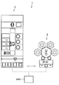
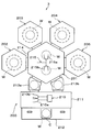
- FIG. 1 is an explanatory diagram showing an outline of a configuration of a substrate processing system 1 according to the present embodiment.
- the substrate processing system 1 includes a coating and developing apparatus 2 that performs photolithography processing on a wafer as a substrate, and an etching processing apparatus 3 that performs etching processing on the wafer.
- a film to be processed (not shown) is formed in advance on the wafer processed by the substrate processing system 1.
- the coating / developing apparatus 2 includes, for example, a cassette station 10 in which a cassette C containing a plurality of wafers W is carried in and out of the outside, and a predetermined type of sheet processing in a photolithography process.
- a processing station 11 having a plurality of various processing apparatuses for processing and an interface station 13 for transferring the wafer W between the exposure apparatus 12 adjacent to the processing station 11 are integrally connected. .
- the cassette station 10 is provided with a cassette mounting table 20.
- the cassette mounting table 20 is provided with a plurality of, for example, four cassette mounting plates 21.
- the cassette mounting plates 21 are arranged in a line in the horizontal X direction (vertical direction in FIG. 2).
- the cassette C can be placed on these cassette placement plates 21 when the cassette C is carried in and out of the coating and developing treatment apparatus 2.
- the cassette station 10 is provided with a wafer transfer device 23 that is movable on a transfer path 22 extending in the X direction.
- the wafer transfer device 23 is also movable in the vertical direction and the vertical axis direction ( ⁇ direction), and includes a cassette C on each cassette mounting plate 21 and a delivery device for a third block G3 of the processing station 11 described later.
- the wafer W can be transferred between the two.
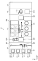
- the processing station 11 is provided with a plurality of, for example, four blocks G1, G2, G3, and G4 having various devices.
- the first block G1 is provided on the front side of the processing station 11 (X direction negative direction side in FIG. 2), and the second side is provided on the back side of the processing station 11 (X direction positive direction side in FIG. 2).
- Block G2 is provided.
- a third block G3 is provided on the cassette station 10 side (Y direction negative direction side in FIG. 1) of the processing station 11, and the interface station 13 side (Y direction positive direction side in FIG. 2) of the processing station 11 is provided. Is provided with a fourth block G4.
- a plurality of liquid processing apparatuses for example, a developing apparatus 30 for developing the wafer W, and a cleaning apparatus 31 for cleaning the wafer W by coating the wafer W with an organic solvent.
- a resist coating device 34 for coating a resist solution to form a resist film and a block copolymer coating device 35 for coating a block copolymer on the wafer W are stacked in order from the bottom.
- the developing device 30, the cleaning device 31, the antireflection film forming device 32, the neutral layer forming device 33, the resist coating device 34, and the block copolymer coating device 35 are arranged side by side in the horizontal direction.
- the number and arrangement of the developing device 30, the cleaning device 31, the antireflection film forming device 32, the neutral layer forming device 33, the resist coating device 34, and the block copolymer coating device 35 can be arbitrarily selected.
- the cleaning device 31, the antireflection film forming device 32, the neutral layer forming device 33, the resist coating device 34, and the block copolymer coating device 35 for example, a spin for applying a predetermined coating solution onto the wafer W. Coating is performed.
- spin coating for example, a coating liquid is discharged onto the wafer W from a coating nozzle, and the wafer W is rotated to diffuse the coating liquid to the surface of the wafer W.
- the block copolymer applied onto the wafer W by the block copolymer coating device 35 includes a first polymer and a second polymer.
- a hydrophobic (nonpolar) polymer having hydrophobicity (no polarity) is used
- a hydrophilic (polarity) polymer having hydrophilicity (polarity) is used.
- PMMA polymethyl methacrylate
- PS polystyrene
- the ratio of the molecular weight of the hydrophilic polymer in the block copolymer is, for example, 40% to 60%, and the ratio of the molecular weight of the hydrophobic polymer in the block copolymer is from 60% to 40%.
- the block copolymer is a polymer obtained by linearly combining these hydrophilic polymer and hydrophobic polymer.
- the neutral layer formed on the wafer W by the neutral layer forming apparatus 33 has an intermediate affinity for the hydrophilic polymer and the hydrophobic polymer.
- a random copolymer or an alternating copolymer of polymethyl methacrylate and polystyrene is used as the neutral layer.
- neutral means having an intermediate affinity for the hydrophilic polymer and the hydrophobic polymer.
- a heat treatment apparatus 40 that performs heat treatment of the wafer W, and a neutral layer treatment that performs surface treatment of the neutral layer by irradiating the neutral layer on the wafer W with ultraviolet rays.
- a polymer separator 44 for separating the coalescence into a hydrophilic polymer and a hydrophobic polymer is provided side by side in the vertical direction and the horizontal direction.
- the heat treatment apparatus 40 includes a hot plate for placing and heating the wafer W and a cooling plate for placing and cooling the wafer W, and can perform both heat treatment and cooling treatment.
- the ultraviolet irradiation device 41 includes a mounting table on which the wafer W is mounted, and an ultraviolet irradiation unit that irradiates the wafer W on the mounting table with ultraviolet light having a wavelength of 172 nm, for example. Further, the number and arrangement of the heat treatment apparatus 40, the ultraviolet irradiation apparatus 41, the adhesion apparatus 42, the peripheral exposure apparatus 43, and the polymer separation apparatus 44 can be arbitrarily selected.
- a plurality of delivery devices 50, 51, 52, 53, 54, 55, 56 are provided in order from the bottom.
- the fourth block G4 is provided with a plurality of delivery devices 60, 61, 62 in order from the bottom.
- a wafer transfer area D is formed in an area surrounded by the first block G1 to the fourth block G4.
- a wafer transfer device 70 is disposed in the wafer transfer region D.
- the wafer transfer device 70 has, for example, a transfer arm that is movable in the Y direction, the X direction, the ⁇ direction, and the vertical direction.
- the wafer transfer device 70 moves in the wafer transfer area D and transfers the wafer W to a predetermined device in the surrounding first block G1, second block G2, third block G3, and fourth block G4. it can.
- a plurality of wafer transfer apparatuses 70 are arranged in the vertical direction, and can transfer the wafer W to a predetermined apparatus having the same height of each of the blocks G1 to G4, for example.
- a shuttle transfer device 80 that transfers the wafer W linearly between the third block G3 and the fourth block G4 is provided.
- the shuttle transport device 80 is linearly movable in the Y direction, for example.
- the shuttle transfer device 80 moves in the Y direction while supporting the wafer W, and can transfer the wafer W between the transfer device 52 of the third block G3 and the transfer device 62 of the fourth block G4.
- a wafer transfer device 100 is provided next to the third block G3 on the positive side in the X direction.
- the wafer transfer apparatus 100 has a transfer arm that is movable in the X direction, the ⁇ direction, and the vertical direction, for example.
- the wafer transfer device 100 can move up and down while supporting the wafer W, and can transfer the wafer W to each delivery device in the third block G3.
- the interface station 13 is provided with a wafer transfer device 110 and a delivery device 111.
- the wafer transfer device 110 has a transfer arm that is movable in the Y direction, the ⁇ direction, and the vertical direction, for example.
- the wafer transfer device 110 can transfer the wafer W between each transfer device, the transfer device 111, and the exposure device 12 in the fourth block G4, for example, by supporting the wafer W on a transfer arm.
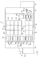
- the etching processing apparatus 3 includes a cassette station 200 that carries the wafer W into and out of the etching processing apparatus 3, a common transport unit 201 that transports the wafer W, and a block copolymer that is phase-separated on the wafer W.
- the cassette station 200 has a transfer chamber 211 in which a wafer transfer mechanism 210 for transferring the wafer W is provided.
- the wafer transfer mechanism 210 has two transfer arms 210a and 210b that hold the wafer W substantially horizontally, and is configured to transfer the wafer W while holding it by either of the transfer arms 210a and 210b.
- a cassette mounting table 212 on which a cassette C capable of accommodating a plurality of wafers W arranged side by side is mounted on the side of the transfer chamber 211. In the illustrated example, a plurality of, for example, three cassettes C can be mounted on the cassette mounting table 212.
- the transfer chamber 211 and the common transfer unit 201 are connected to each other via two load lock devices 213a and 213b that can be evacuated.
- the common transfer unit 201 includes a transfer chamber chamber 214 having a sealable structure formed to have a substantially polygonal shape (in the illustrated example, a hexagonal shape) as viewed from above, for example.
- a wafer transfer mechanism 215 for transferring the wafer W is provided in the transfer chamber 214.
- the wafer transfer mechanism 215 has two transfer arms 215a and 215b that hold the wafer W substantially horizontally, and is configured to transfer the wafer W while holding the wafer W by either of the transfer arms 215a and 215b. .
- Etching devices 202, 203, 204, 205 and load lock devices 213 b, 213 a are arranged outside the transfer chamber chamber 214 so as to surround the periphery of the transfer chamber chamber 214.
- the etching devices 202, 203, 204, 205 and the load lock devices 213b, 213a are arranged in this order in the clockwise direction when viewed from above, for example, and face the six side portions of the transfer chamber 214, respectively. Are arranged.
- etching apparatuses 202 to 205 for example, a RIE (Reactive Ion Etching) apparatus is used, for example. That is, in the etching apparatuses 202 to 205, dry etching for etching a hydrophobic polymer or a film to be processed is performed by a reactive gas (etching gas) such as oxygen (O 2 ), ions, or radicals, for example.
- etching gas reactive gas
- oxygen (O 2 ) oxygen
- ions oxygen (O 2 )
- radicals for example.
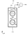
- FIG. 6 is a cross-sectional view showing an outline of the configuration of the polymer separation device 44
- FIG. 7 is a vertical cross-sectional view showing an outline of the configuration of the polymer separation device 44.
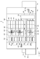
- the polymer separation device 44 has a processing container 170 capable of closing the inside, and a loading / unloading port 171 for the wafer W is formed on a side surface of the processing container 170 facing the wafer transfer device 70.
- the polymer separation device 44 is a heat treatment device having a heat plate 172 for placing and heating the wafer W in the processing container 170 and a cooling plate 173 for placing and adjusting the temperature of the wafer W. And cooling treatment can be performed.
- the hot plate 172 has a substantially disk shape with a thickness.
- the hot plate 172 has a horizontal upper surface, and a suction port (not shown) for sucking the wafer W, for example, is provided on the upper surface. By suction from the suction port, the wafer W can be sucked and held on the hot plate 172.
- an electric heater 174 as a heating mechanism is provided inside the heat plate 172.
- the plate 172 can be controlled to a predetermined set temperature.
- the heat plate 172 has a plurality of through holes 175 penetrating in the vertical direction.
- a lift pin 176 is provided in the through hole 175.
- the lift pins 176 can be moved up and down by a lift drive mechanism 177 such as a cylinder.
- the elevating pins 176 are inserted through the through holes 175 and protrude from the upper surface of the hot plate 172 so that the elevating pins 176 can move up and down while supporting the wafer W.
- the hot plate 172 is provided with an annular holding member 178 that holds the outer periphery of the hot plate 172.
- the holding member 178 is provided with a cylindrical support ring 179 that surrounds the outer periphery of the holding member 178 and accommodates the lifting pins 176.
- the cooling plate 173 has a thick and substantially disk shape.
- the cooling plate 173 has a horizontal upper surface, and a suction port (not shown) for sucking, for example, the wafer W is provided on the upper surface. By suction from this suction port, the wafer W can be sucked and held on the cooling plate 173.
- a cooling member such as a Peltier element is built in the cooling plate 173, and the cooling plate 173 can be adjusted to a predetermined set temperature.
- the cooling plate 173 has the same configuration as the hot plate 172. That is, the cooling plate 173 is formed with a plurality of through holes 180 penetrating in the vertical direction. Elevating pins 181 are provided in the through hole 180. The lift pins 181 can be moved up and down by a lift drive mechanism 182 such as a cylinder. The elevating pins 181 are inserted through the through-holes 180 and project from the upper surface of the cooling plate 173 so that the elevating pins 181 can move up and down while supporting the wafer W.
- a lift drive mechanism 182 such as a cylinder.
- the elevating pins 181 are inserted through the through-holes 180 and project from the upper surface of the cooling plate 173 so that the elevating pins 181 can move up and down while supporting the wafer W.
- the cooling plate 173 is provided with an annular holding member 183 that holds the outer periphery of the cooling plate 173.
- the holding member 183 is provided with a cylindrical support ring 184 that surrounds the outer periphery of the holding member 183 and accommodates the lifting pins 181.
- a gas supply port 190 for supplying a processing gas into the processing container 170 is formed on the side surface of the processing container 170 opposite to the loading / unloading port 171.
- a gas supply source 192 is connected to the gas supply port 190 via a gas supply pipe 191.
- the gas supply pipe 191 is provided with a flow rate adjusting mechanism 193 so that the amount of processing gas supplied from the gas supply source 192 into the processing container 170 can be adjusted.
- the flow rate adjusting mechanism 193 is controlled by the control unit 300 described later.
- the processing gas does not oxidize the polymer when the wafer W is heat-treated and the block copolymer applied on the wafer W by the block copolymer coating device 35 is phase-separated into a hydrophilic polymer and a hydrophobic polymer.
- a non-oxidizing gas is used.
- a gas not containing oxygen such as nitrogen gas or argon gas, is used.
- the configuration of the heat treatment apparatus 40 is the same as that of the polymer separation apparatus 44 except that the gas supply port 190 is not formed in the processing container 170.
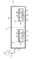
- the substrate processing system 1 described above is provided with a control unit 300 as shown in FIG.
- the control unit 300 is a computer, for example, and has a program storage unit (not shown).
- the program storage unit stores a program for controlling the processing of the wafer W in the substrate processing system 1.
- the program storage unit also stores a program for controlling the operation of drive systems such as the above-described various processing apparatuses and transfer apparatuses to realize substrate processing described later in the substrate processing system 1.
- the program is recorded on a computer-readable storage medium such as a computer-readable hard disk (HD), flexible disk (FD), compact disk (CD), magnetic optical desk (MO), or memory card. Or installed in the control unit 300 from the storage medium.
- HD computer-readable hard disk
- FD flexible disk
- CD compact disk
- MO magnetic optical desk
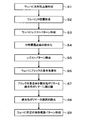
- FIG. 8 is a flowchart showing an example of main steps of such wafer processing.
- a cassette C containing a plurality of wafers W is carried into the cassette station 10 of the coating and developing treatment apparatus 2 and placed on a predetermined cassette placing plate 21. Thereafter, the wafers W in the cassette C are sequentially taken out by the wafer transfer device 23 and transferred to the transfer device 53 of the processing station 11.
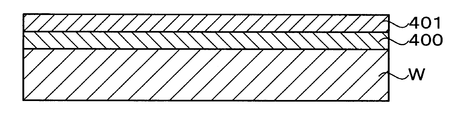
- the wafer W is transferred to the heat treatment apparatus 40 by the wafer transfer apparatus 70 and the temperature is adjusted. Thereafter, the wafer W is transferred to the antireflection film forming apparatus 32 by the wafer transfer apparatus 70, and an antireflection film 400 is formed on the wafer W as shown in FIG. 9 (step S1 in FIG. 8). Thereafter, the wafer W is transferred to the heat treatment apparatus 40, heated, and the temperature is adjusted.
- the wafer W is transferred to the neutral layer forming device 33 by the wafer transfer device 70.
- a neutral agent is applied on the antireflection film 400 of the wafer W to form a neutral layer 401 as a base film (step S2 in FIG. 8).
- the wafer W is transferred to the heat treatment apparatus 40, heated, temperature-controlled, and then returned to the delivery apparatus 53.
- the heating temperature of the wafer W after the neutral layer 401 is formed in the heat treatment apparatus 40 is preferably approximately 200 ° C. to 300 ° C., and in this embodiment, for example, approximately 250 ° C.
- the wafer W is transferred to the delivery device 54 by the wafer transfer device 100. Thereafter, the wafer W is transferred to the adhesion device 42 by the wafer transfer device 70 and subjected to an adhesion process. Thereafter, the wafer W is transferred to the resist coating device 34 by the wafer transfer device 70, and a resist solution is applied onto the neutral layer 401 of the wafer W to form a resist film. Thereafter, the wafer W is transferred to the heat treatment apparatus 40 by the wafer transfer apparatus 70 and pre-baked. Thereafter, the wafer W is transferred to the delivery device 55 by the wafer transfer device 70.
- the wafer W is transferred to the peripheral exposure device 43 by the wafer transfer device 70 and subjected to peripheral exposure processing. Thereafter, the wafer W is transferred to the delivery device 56 by the wafer transfer device 70.
- the wafer W is transferred to the transfer device 52 by the wafer transfer device 100 and transferred to the transfer device 62 by the shuttle transfer device 80.
- the wafer W is transferred to the exposure apparatus 12 by the wafer transfer apparatus 110 of the interface station 13 and subjected to exposure processing.
- the wafer W is transferred from the exposure apparatus 12 to the delivery apparatus 60 by the wafer transfer apparatus 110. Thereafter, the wafer W is transferred to the heat treatment apparatus 40 by the wafer transfer apparatus 70 and subjected to post-exposure baking. Thereafter, the wafer W is transferred to the developing device 30 by the wafer transfer device 70 and developed. After the development is completed, the wafer W is transferred to the heat treatment apparatus 40 by the wafer transfer apparatus 70 and subjected to a post-bake process.
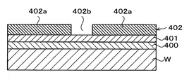
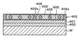
- a predetermined resist pattern 402 is formed on the neutral layer 401 of the wafer W as shown in FIG. 10 (step S3 in FIG. 8).
- the resist pattern 402 has a linear shape in plan view.
- the width of the space portion 402b is set so that the hydrophilic polymer 405 and the hydrophobic polymer 406 are alternately arranged in the odd number layers in the space portion 402b as described later.
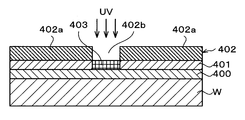
- the wafer W on which the resist pattern 402 is formed is transferred to the ultraviolet irradiation device 41 by the wafer transfer device 70.
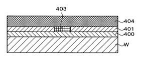
- the ultraviolet irradiation device 41 as shown in FIG. 11, the exposed surface of the neutral layer 401 exposed from the resist pattern 402 (space portion 402b) is irradiated with ultraviolet rays. At this time, ultraviolet rays having a wavelength of 172 nm are irradiated. Then, the exposed surface of the neutral layer 401 is oxidized and hydrophilized (step S4 in FIG. 8).
- the region of the neutral layer 401 thus made hydrophilic may be referred to as a hydrophilic region 403.
- the wavelength of ultraviolet rays for forming the hydrophilic region 403 in the neutral layer 401 may be 300 nm or less.
- active oxygen can be generated from oxygen in the processing atmosphere, and the exposed surface of the neutral layer 401 is oxidized and hydrophilized by this active oxygen.
- active oxygen in order to generate
- the wavelength of ultraviolet rays is 172 nm, not only when ozone is used as a processing atmosphere, but also when the processing atmosphere is an air atmosphere, active oxygen can be efficiently generated from oxygen in the air atmosphere. I know it.
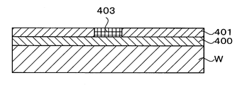
- the wafer W is transferred to the cleaning device 31 by the wafer transfer device 70.
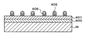
- the cleaning device 31 an organic solvent is supplied onto the wafer W, and the resist pattern 402 on the wafer W is removed as shown in FIG. 12 (step S5 in FIG. 8).
- the neutral layer 401 the surface of the hydrophilic region 403 has hydrophilicity, and the surface of other regions has neutrality. And the surface of the neutral layer 401 is maintained flat.
- the wafer W is transferred to the delivery device 50 by the wafer transfer device 70.
- the wafer W is transferred to the delivery device 55 by the wafer transfer device 100. Thereafter, the wafer W is transferred to the block copolymer coating device 35 by the wafer transfer device 70.
- the block copolymer coating device 35 the block copolymer 404 is coated on the neutral layer 401 of the wafer W as shown in FIG. 13 (step S6 in FIG. 8). At this time, since the surface of the neutral layer 401 is kept flat, the block copolymer 404 is also applied so as to have a uniform film thickness.
- the wafer W is transferred to the polymer separation device 44 by the wafer transfer device 70 and placed on the hot platen 172.
- nitrogen gas is supplied as a non-oxidizing gas into the processing container 170 of the polymer separator 44.
- the flow rate adjusting mechanism 193 is controlled by the controller 300, and the oxygen concentration in the processing container 170 is adjusted to 30 ppm to 50 ppm.
- the wafer W is first heat-treated by the hot plate 172.
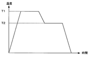
- a temperature pattern shown in FIG. 14 is used.
- the vertical axis represents the temperature of the hot plate 172
- the horizontal axis represents the heat treatment time.
- the temperature of the hot plate 172 is raised to the first temperature T1 and held for a certain time.
- the polymer is diffused by the heat treatment at the first temperature T1.
- the first temperature in the present embodiment is, for example, 350 ° C.
- the first temperature is preferably set to a temperature equal to or higher than the order-disorder transition temperature (TOD) of the block copolymer. Volatilizes at temperatures below TOD. Therefore, it is preferable that the first temperature be as high as possible below the volatilization temperature of the polymer.
- TOD order-disorder transition temperature
- the hot plate 172 is lowered to the second temperature T2 lower than the first temperature T1, as shown in FIG.
- the block copolymer 404 on the wafer W is phase-separated into a hydrophilic polymer 405 and a hydrophobic polymer 406 as shown in FIGS. 8 step S7).
- the second temperature in the present embodiment is 170 ° C., for example.
- the molecular weight ratio of the hydrophilic polymer 405 is 40% to 60%
- the molecular weight ratio of the hydrophobic polymer 406 is 60% to 40%.
- step S6 as shown in FIGS. 15 and 16, the hydrophilic polymer 405 and the hydrophobic polymer 406 are phase-separated into a lamellar structure.
- the width of the space portion 402b of the resist pattern 402 is formed to a predetermined width in the above-described step S3
- the hydrophilic polymer 405 and the hydrophobic polymer 406 are formed on the hydrophilic region 403 of the neutral layer 401. Alternatingly arranged in odd layers, for example, three layers.
- the hydrophilic polymer 405 is disposed in the middle on the hydrophilic region 403, and the hydrophobic polymers 406 and 406 are disposed on both sides thereof. And the hydrophilic polymer 405 and the hydrophobic polymer 406 are alternately arrange
- the wafer W is transferred to the delivery device 50 by the wafer transfer device 70, and then transferred to the cassette C of the predetermined cassette mounting plate 21 by the wafer transfer device 23 of the cassette station 10.
- the cassette C containing the wafer W is unloaded from the coating and developing treatment apparatus 2 and then loaded into the etching processing apparatus 3.
- the etching processing apparatus 3 first, one wafer W is taken out from the cassette C on the cassette mounting table 212 by the wafer transfer mechanism 210 and loaded into the load lock apparatus 213 a.
- the inside of the load lock device 213a is sealed and decompressed.
- the inside of the load lock device 213a and the inside of the transfer chamber chamber 214 evacuated to a predetermined degree of vacuum are communicated.
- the wafer transfer mechanism 215 unloads the wafer W from the load lock device 213a and loads it into the transfer chamber 214.
- the wafer W carried into the transfer chamber 214 is then transferred to the etching apparatus 202 by the wafer transfer mechanism 215.
- the wafer W is etched, and the hydrophilic polymer 405 is selectively removed as shown in FIG. 17 to form a predetermined pattern of the hydrophobic polymer 406 (step S8 in FIG. 8).
- the pattern height of the hydrophobic polymer 406 is also uniform.
- the wafer W is transferred to the etching apparatus 204 by the wafer transfer mechanism 215.
- the film to be processed on the wafer W is etched using the hydrophobic polymer 406 on the wafer W as a mask.
- the hydrophobic polymer 406 and the antireflection film are removed, and a predetermined pattern is formed on the film to be processed (step S9 in FIG. 8).
- the wafer W is returned again into the transfer chamber 214 by the wafer transfer mechanism 215. Then, the wafer is transferred to the wafer transfer mechanism 210 via the load lock device 213b and stored in the cassette C. Thereafter, the cassette C containing the wafers W is unloaded from the etching processing apparatus 3 and a series of wafer processing ends.
- the block copolymer 404 on the wafer W is heat-treated in the non-oxidizing gas atmosphere in step S7, the hydrophilic polymer 405 and the hydrophobic polymer 406 of the block copolymer 404 are oxidized. Can be prevented. Therefore, pattern variations due to oxidation of the hydrophilic polymer 405 and the hydrophobic polymer 406 can be prevented, and a predetermined fine pattern can be formed on the wafer W. As a result, in the process S9, the processing target film can be appropriately etched using the pattern as a mask, and a predetermined pattern can be formed on the processing target film.
- step S7 since the block copolymer 404 on the wafer W is first heat-treated at the first temperature T1, diffusion of the polymers 405 and 406 can be promoted to form a longer pattern.
- the polymers 405 and 406 are required to be arranged without variation along the longitudinal direction of the line portion 402a of the resist pattern 402, and thus heat treatment is performed at the first temperature T1. It is effective.
- the neutral layer is also etched using the resist pattern as a mask.
- the surface from which the neutral layer has been removed has hydrophilicity due to the exposure of the antireflection film, and the surface on which the neutral layer remains has neutrality.
- the wafer W has to be once taken out of the coating and developing treatment apparatus 2 and transferred to the etching treatment apparatus 3.
- step S4 the ultraviolet irradiation device 41 in the coating and developing treatment apparatus 2 irradiates the exposed surface of the neutral layer 401 with ultraviolet irradiation, thereby surface-treating the neutral layer 401 to make it hydrophilic.
- the neutral layer is also etched using the resist pattern as a mask. As a result, the surface from which the neutral layer has been removed has hydrophilicity due to the exposure of the antireflection film, and the surface on which the neutral layer remains has neutrality.
- the wafer W in order to etch the neutral layer, the wafer W has to be once taken out of the coating and developing treatment apparatus 2 and transferred to the etching treatment apparatus 3.
- the neutral layer 401 is made hydrophilic by irradiating with ultraviolet rays in this embodiment, the transfer of the wafer W from the coating / developing apparatus 2 to the etching apparatus 3 can be omitted.
- the wafer processing in steps S1 to S7 is performed by one coating and developing processing apparatus 2. Therefore, the throughput of wafer processing in the substrate processing system 1 can be improved.
- the exposed surface of the neutral layer 401 is irradiated with ultraviolet rays in step S4 to make the exposed surface hydrophilic, but the means for making the exposed surface hydrophilic is not limited to this.
- a hydrophilic film having hydrophilicity may be formed on the exposed surface of the neutral layer 401.
- the exposed surface of the neutral layer 401 is made hydrophilic, but the exposed surface may be hydrophobized as a surface treatment.
- the hydrophobic polymer 406 is disposed in the middle of the hydrophobized region, and the hydrophilic polymers 405 and 405 are disposed on both sides thereof.
- the hydrophilic polymer 405 and the hydrophobic polymer 406 are alternately arranged in an arrangement opposite to the case where the exposed surface of the neutral layer 401 is made hydrophilic.
- the so-called dry etching process is performed in the etching processing apparatus 3 to selectively remove the hydrophilic polymer 405, but the hydrophilic polymer 405 may be removed by a wet etching process.
- the wafer W obtained by phase separation of the block copolymer 404 in step S7 is transferred to the ultraviolet irradiation device 41 in place of the etching processing apparatus 3 in step S8. Then, by irradiating the wafer W with ultraviolet rays, the bonding chain of polymethyl methacrylate, which is the hydrophilic polymer 405, is cut, and the polystyrene, which is the hydrophobic polymer 406, is crosslinked. Thereafter, the wafer W is transferred to the cleaning device 31, and isopropyl alcohol (IPA), for example, is supplied to the wafer W in the cleaning device 31. As a result, the hydrophilic polymer 405 having the bond chain cleaved by ultraviolet irradiation is dissolved and removed.
- IPA isopropyl alcohol
- the selective ratio between the hydrophilic polymer 405 and the hydrophobic polymer 406 is, for example, about 3 to 7: 1.
- the hydrophilic polymer 405 is removed by so-called wet etching using an organic solvent, since the hydrophobic polymer 406 is hardly dissolved in the organic solvent, film slippage can be avoided. As a result, a sufficient film thickness as a mask can be ensured when etching the film to be processed using the pattern of the hydrophobic polymer 406 as a mask in subsequent steps.
- the transfer of the wafer W from the coating and developing treatment apparatus 2 to the etching treatment apparatus 3 can be omitted. Therefore, the throughput of wafer processing in the substrate processing system 1 can be improved.
- polymethyl methacrylate is used as the hydrophilic polymer, but other polymers may be used as the hydrophilic polymer.
- polydimethylsiloxane PDMS
- PDMS polydimethylsiloxane
- the molecular weight ratio of the hydrophilic polymer 405 in the block copolymer 404 is 20% to 40%
- the molecular weight ratio of the hydrophobic polymer 406 is 80% to 60%. is there.
- the substrate processing system 1 having the same structure as that of the above embodiment is used.
- step S6 since the pattern of the polymers 405 and 406 is formed using the resist pattern formed in step S3 as a guide, the surface treatment (hydrophilization) of the neutral layer 401 in step S4 and the resist pattern removal in step S5 are performed.
- the block copolymer 404 is directly applied to the resist pattern formed in step S3 (step S6).
- step S7 the block copolymer 404 is heat-treated with the polymer separator 44.
- the inside of the processing container 170 of the polymer separator 44 is a non-oxidizing atmosphere.
- the cross-sectional shape of the cylinder structure in which the hydrophobic polymer 406 is sandwiched between the upper and lower surfaces of the hydrophilic polymer 405 and the hydrophilic polymer 405 is circularly arranged inside the hydrophobic polymer 406. Phase separation is carried out into a hydrophilic polymer 405 and a hydrophobic polymer 406.
- the cylinder structure as shown in FIG.
- the surface tension of polydimethylsiloxane used for the hydrophilic polymer 405 is much smaller than that of polystyrene used for the hydrophobic polymer 406, and is layered along the surface of the neutral layer 401. This is for phase separation.
- the hydrophilic polymer 405 is phase-separated also on the atmosphere side, and the hydrophobic polymer 406 is phase-separated in a form sandwiched between the hydrophilic polymers 405.
- the hydrophilic polymer 405 has a molecular weight ratio of 40% to 60%
- the hydrophobic polymer 406 has a molecular weight ratio of 60% to 40%.
- a cylindrical shape is formed inside the hydrophobic polymer 406.
- step S8 for example, the organic solvent is supplied to the hydrophilic polymer 405 formed in a layered manner on the atmosphere side by the cleaning device 31, and the hydrophilic polymer 405 is removed.
- the resist pattern 402 and the hydrophobic polymer 406 are selectively removed from the wafer W by the etching processing apparatus 3, and as shown in FIG. 20, the cylindrical hydrophilic polymer 405 and the hydrophobic polymer 406 remaining in the lower portion thereof. As a result, a pattern is formed.
- the block copolymer 404 can be appropriately phase-separated into the hydrophilic polymer 405 and the hydrophobic polymer 406 having a cylindrical structure, and the etching process of the film to be processed can be appropriately performed.
- the film to be processed on the wafer W is etched in step S9, but the wafer processing method of the present invention can also be applied when etching the wafer W itself.
- the hot plate 172 and the cooling plate 173 are disposed in the processing container 170.
- the non-oxidizing gas atmosphere is set on the wafer W by the hot plate 172. Therefore, for example, only the heat plate 172 may be disposed in a processing container whose inside can be closed. In such a case, since the supply amount of the non-oxidizing gas can be reduced, the running cost of the polymer separator can be reduced.
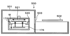
- FIG. 21 is a longitudinal sectional view showing an outline of a configuration of a polymer separation apparatus 500 according to another embodiment
- FIG. 22 is a transverse sectional view showing an outline of a structure of the polymer separation apparatus 500.
- the description is abbreviate
- the polymer separation apparatus 500 includes a housing 501, and a cooling plate 502 for placing the wafer W and adjusting the temperature is provided on the wafer transportation device 70 side of the housing 501, and the wafer transportation device sandwiching the cooling plate 502.
- a heat plate 172 is provided on the side opposite to the 70 side.
- the ceiling portion is opened over the entire surface, and only the heat plate 172 side is formed in a container shape having a ceiling.
- a conveyance port 503 through which the cooling plate 502 passes is formed between the cooling plate 502 and the hot plate 172 of the housing 501.
- the cooling plate 502 has a substantially rectangular flat plate shape as shown in FIG. 22, and the end surface on the hot plate 172 side is curved in an arc shape.
- Two slits 510 are formed in the cooling plate 502 along the Y direction.
- the slit 510 is formed from the end surface of the cooling plate 502 on the hot plate 172 side to the vicinity of the center of the cooling plate 502.
- the slit 510 can prevent the cooling plate 502 from interfering with the lift pins 176 and 181.
- the cooling plate 502 incorporates a temperature adjusting member (not shown) such as a Peltier element.
- the cooling plate 502 is supported by a support arm 511 as shown in FIG.
- a drive unit 512 is attached to the support arm 511.
- the drive unit 512 is attached to a rail 513 extending in the Y direction.
- the rail 513 extends from the lower side of the cooling plate 502 to the vicinity of the lower side of the transfer port 503.
- the cooling plate 502 can be moved along the rail 513 to above the heat plate 172.
- the cooling plate 502 also functions as a transfer mechanism that transfers the wafer W to and from the hot plate 172.
- a cylindrical lid 520 having the same diameter as that of the support ring 179 is provided above the hot plate 172, for example.
- a gas supply port 190 is formed near the center of the ceiling of the lid 520, and a gas supply source 192 is connected to the gas supply port 190.
- the gas supply port 190 is provided with a supply nozzle 521 formed in a substantially disc shape.
- a supply port (not shown) is formed in the outer peripheral portion of the supply nozzle 521, and the non-oxidizing gas supplied from the gas supply source 192 can be supplied radially in the diameter direction of the wafer.
- the lid body 520 is formed so as to be movable up and down by a lifting mechanism (not shown). For example, as shown in FIG. By doing so, the space surrounded by the holding member 178, the support ring 179, the heat plate 172, and the lid body 520 can be almost sealed. Therefore, by supplying the non-oxidizing gas from the gas supply source 192 with the lid 520 being in contact with the support ring 179, the wafer W on the hot plate 172 is non-oxidizing with the minimum non-oxidizing gas. It can be covered with a gas atmosphere. In such a case, the holding member 178, the support ring 179, the hot plate 172, and the lid 520 function as a processing container capable of sealing the inside. For example, an exhaust port (not shown) is formed on the upper surface of the holding member 178, and the non-oxidizing gas supplied from the gas supply source 192 can be exhausted.
- an oxygen concentration detection mechanism 522 is provided on the bottom surface of the lid 520, for example, the ceiling. The detection result of the oxygen concentration detection mechanism 522 is input to the control unit 300.
- the polymer separating apparatus 500 is configured as described above. Next, processing of the wafer W in the polymer separating apparatus 500 will be described with reference to FIGS. In FIG. 23 to FIG. 27, only main devices are shown.
- the wafer W is delivered to the cooling plate 502 by the wafer transfer apparatus 70 as shown in FIG.
- the cooling plate 502 is moved upward through the transport port 503.
- the lid 520 stands by above the hot plate 172 so that the hot plate 172 can pass below the lid 520. Further, the hot plate 172 has been heated to the first temperature T1 in advance.
- the elevating pins 176 are raised, the wafer W is transferred to the elevating pins 175, and then the cooling plate 502 is retracted from below the lid 520. Thereafter, the lid body 520 descends and the lower end surface of the lid body 520 comes into contact with the upper surface of the support ring 179. Thereafter, nitrogen gas as a non-oxidizing gas is supplied from the supply nozzle 521. The space surrounded by the lid 520 and the hot plate 172 is gradually replaced with a non-oxidizing gas. In parallel with the lowering of the lid body 520, the elevating pins 176 are lowered. At this time, as shown in FIG.
- the elevating pins 176 are maintained for a certain time in a state where the wafer W is separated from the upper surface of the hot plate 172 by a predetermined distance.
- the distance between the wafer W and the hot plate 172 at this time is adjusted to a distance such that the temperature of the wafer W does not exceed 200 ° C., for example.
- the wafer W is placed on the hot plate 172 before the atmosphere around the wafer W is replaced with the non-oxidizing gas, and the hydrophilic polymer 405 and the hydrophobic polymer 406 of the block copolymer 404 are oxidized. Can be prevented.
- the elevating pins 176 are further lowered, and as shown in FIG. W is placed on the hot plate 172.
- the time for which the wafer W is maintained at a predetermined distance from the upper surface of the hot plate 172 may be determined based on a measurement result by the oxygen concentration detection mechanism 522, or may be determined based on a test performed in advance. The time when the concentration is 50 ppm or less may be obtained and determined.
- each device operates in the reverse order of FIGS. 23 to 25, so that the wafer W is delivered to the cooling plate 502. Thereafter, the wafer W is cooled by the cooling plate 502 for a predetermined time to adjust the temperature, and the processing in the polymer separation apparatus 500 is completed.
- the non-oxidizing gas is supplied only to the space surrounded by the lid 520 and the hot plate 172.
- the running cost can be reduced.
- the wafer W is maintained for a predetermined time in a state where it is separated from the upper surface of the hot plate 172 by a predetermined distance. More specifically, the oxygen concentration is given in a space surrounded by the lid 520 and the hot plate 172. Until the value is reached, the wafer W is not placed on the hot platen 172, so that the hydrophilic polymer 405 and the hydrophobic polymer 406 of the block copolymer 404 can be prevented from being oxidized.
- the neutral layer 401 is used as the base film of the block copolymer 404, but the type of base film is not limited to this embodiment.
- polystyrene that is a hydrophobic polymer and crosslinked by heating at a predetermined temperature, for example, 350 ° C. may be used as the base film.
- the neutral layer 401 and polystyrene used as a base film vary in surface properties when oxidized by heating.
- a neutral portion and a non-neutral portion are generated on the neutral layer 401, or in the case of polystyrene, for example, the portion having hydrophobicity and not having hydrophobicity. Part may occur. Therefore, in order to more efficiently suppress the oxidation of the neutral layer 401 or the polystyrene film as the base film, the heat treatment performed after the step S2 and before the step S3 is performed in a non-oxidizing gas atmosphere.
- the heat treatment may be performed using a base film forming apparatus.
- the above-described polymer separation apparatus 44 or polymer separation apparatus 500 may be used, or another heat treatment apparatus having the same configuration as the polymer separation apparatuses 44 and 500 may be used.
- the oxidation of the base film is dominant as a cause of pattern variations, for example, only the heat treatment performed in the base film forming apparatus after the step S2 and before the step S3 is performed in a non-oxidizing gas atmosphere.
- the heat treatment in step S7 may be performed in an atmosphere other than the non-oxidizing gas.
- a nozzle for supplying polystyrene to a liquid processing apparatus such as the neutral layer forming apparatus 33 may be provided, or a polystyrene coating apparatus for forming a polystyrene film by applying polystyrene. May be provided separately.
- the configuration of the polystyrene coating device may be the same as that of other liquid processing devices such as the neutral layer forming device 33 and the block copolymer coating device 35.
- the present invention is not limited to such examples. It is obvious for those skilled in the art that various changes or modifications can be conceived within the scope of the idea described in the claims, and these are naturally within the technical scope of the present invention. It is understood.
- the present invention is not limited to this example and can take various forms.
- the present invention can also be applied to a case where the substrate is another substrate such as an FPD (flat panel display) other than a wafer or a mask reticle for a photomask.
- FPD flat panel display
- the present invention is useful when a substrate is treated with a block copolymer containing, for example, a hydrophilic polymer having hydrophilicity and a hydrophobic polymer having hydrophobicity.
Landscapes
- Engineering & Computer Science (AREA)
- Physics & Mathematics (AREA)
- General Physics & Mathematics (AREA)
- Condensed Matter Physics & Semiconductors (AREA)
- Manufacturing & Machinery (AREA)
- Computer Hardware Design (AREA)
- Microelectronics & Electronic Packaging (AREA)
- Power Engineering (AREA)
- Chemical & Material Sciences (AREA)
- General Chemical & Material Sciences (AREA)
- Chemical Kinetics & Catalysis (AREA)
- Plasma & Fusion (AREA)
- Analytical Chemistry (AREA)
- Photosensitive Polymer And Photoresist Processing (AREA)
- Life Sciences & Earth Sciences (AREA)
- Wood Science & Technology (AREA)
- Materials For Photolithography (AREA)
- Application Of Or Painting With Fluid Materials (AREA)
- Coating Apparatus (AREA)
- Exposure Of Semiconductors, Excluding Electron Or Ion Beam Exposure (AREA)
- Programmable Controllers (AREA)
Priority Applications (2)
| Application Number | Priority Date | Filing Date | Title |
|---|---|---|---|
| US14/430,574 US20150228512A1 (en) | 2012-10-02 | 2013-09-30 | Substrate treatment method, computer-readable storage medium, and substrate treatment system |
| KR1020157008388A KR101967503B1 (ko) | 2012-10-02 | 2013-09-30 | 기판 처리 방법, 컴퓨터 기억 매체 및 기판 처리 시스템 |
Applications Claiming Priority (4)
| Application Number | Priority Date | Filing Date | Title |
|---|---|---|---|
| JP2012-220819 | 2012-10-02 | ||
| JP2012220819 | 2012-10-02 | ||
| JP2013-170120 | 2013-08-20 | ||
| JP2013170120A JP6141144B2 (ja) | 2012-10-02 | 2013-08-20 | 基板処理方法、プログラム、コンピュータ記憶媒体及び基板処理システム |
Publications (1)
| Publication Number | Publication Date |
|---|---|
| WO2014054570A1 true WO2014054570A1 (ja) | 2014-04-10 |
Family
ID=50434897
Family Applications (1)
| Application Number | Title | Priority Date | Filing Date |
|---|---|---|---|
| PCT/JP2013/076511 Ceased WO2014054570A1 (ja) | 2012-10-02 | 2013-09-30 | 基板処理方法、コンピュータ記憶媒体及び基板処理システム |
Country Status (5)
| Country | Link |
|---|---|
| US (1) | US20150228512A1 (enExample) |
| JP (1) | JP6141144B2 (enExample) |
| KR (1) | KR101967503B1 (enExample) |
| TW (1) | TWI569307B (enExample) |
| WO (1) | WO2014054570A1 (enExample) |
Families Citing this family (7)
| Publication number | Priority date | Publication date | Assignee | Title |
|---|---|---|---|---|
| JP5919210B2 (ja) * | 2012-09-28 | 2016-05-18 | 東京エレクトロン株式会社 | 基板処理方法、プログラム、コンピュータ記憶媒体及び基板処理システム |
| WO2016125408A1 (ja) * | 2015-02-05 | 2016-08-11 | 東京エレクトロン株式会社 | 研磨装置、塗布膜形成装置、塗布膜形成方法、記憶媒体、パターン形成方法及びパターン形成装置 |
| JP6267143B2 (ja) * | 2015-03-05 | 2018-01-24 | 東京エレクトロン株式会社 | 基板処理方法、プログラム、コンピュータ記憶媒体及び基板処理システム |
| TWI723052B (zh) * | 2015-10-23 | 2021-04-01 | 日商東京威力科創股份有限公司 | 基板處理方法、程式及電腦記憶媒體 |
| JP7030414B2 (ja) * | 2017-02-14 | 2022-03-07 | 株式会社Screenホールディングス | 基板処理方法及びその装置 |
| JP6896447B2 (ja) * | 2017-02-14 | 2021-06-30 | 株式会社Screenホールディングス | 基板処理方法 |
| JP6914048B2 (ja) | 2017-02-14 | 2021-08-04 | 株式会社Screenホールディングス | 基板処理方法 |
Citations (9)
| Publication number | Priority date | Publication date | Assignee | Title |
|---|---|---|---|---|
| US20030091752A1 (en) * | 2001-10-05 | 2003-05-15 | Nealey Paul F. | Guided self-assembly of block copolymer films on interferometrically nanopatterned substrates |
| JP2004099667A (ja) * | 2002-09-05 | 2004-04-02 | Kansai Tlo Kk | 垂直配向ラメラ構造を有するブロック共重合体膜作製方法 |
| JP2005257923A (ja) * | 2004-03-10 | 2005-09-22 | National Institute Of Advanced Industrial & Technology | リソグラフィーマスク及び微細パターンを作製する方法 |
| JP2007138052A (ja) * | 2005-11-18 | 2007-06-07 | Kyoto Univ | 高分子薄膜、パターン基板の製造方法、パターン転写体、及び磁気記録用パターン媒体 |
| JP2007313568A (ja) * | 2006-05-23 | 2007-12-06 | Kyoto Univ | 微細構造体、パターン媒体、及びそれらの製造方法 |
| JP2008036491A (ja) * | 2006-08-03 | 2008-02-21 | Nippon Telegr & Teleph Corp <Ntt> | パターン形成方法及びモールド |
| JP2010056256A (ja) * | 2008-08-28 | 2010-03-11 | Hitachi Ltd | 微細構造を有する高分子薄膜およびパターン基板の製造方法 |
| JP2010522643A (ja) * | 2007-02-08 | 2010-07-08 | マイクロン テクノロジー, インク. | サブリソグラフィックパターニングのためにブロック共重合体自己集合を使用する方法 |
| JP2012066536A (ja) * | 2010-09-27 | 2012-04-05 | Hitachi Ltd | シルセスキオキサンを有する高分子薄膜、微細構造体及びこれらの製造方法 |
Family Cites Families (6)
| Publication number | Priority date | Publication date | Assignee | Title |
|---|---|---|---|---|
| JP2002137321A (ja) * | 2000-11-01 | 2002-05-14 | Ube Ind Ltd | 複合体薄膜とその製造方法 |
| JP3741604B2 (ja) * | 2000-11-27 | 2006-02-01 | 東京エレクトロン株式会社 | 熱処理装置および熱処理方法 |
| US6864692B1 (en) * | 2002-06-20 | 2005-03-08 | Xsilogy, Inc. | Sensor having improved selectivity |
| US7347953B2 (en) * | 2006-02-02 | 2008-03-25 | International Business Machines Corporation | Methods for forming improved self-assembled patterns of block copolymers |
| TWI355970B (en) * | 2007-01-19 | 2012-01-11 | Tokyo Electron Ltd | Coating treatment apparatus, substrate treatment s |
| JP2010234703A (ja) * | 2009-03-31 | 2010-10-21 | Fujifilm Corp | 積層体 |
-
2013
- 2013-08-20 JP JP2013170120A patent/JP6141144B2/ja active Active
- 2013-09-26 TW TW102134810A patent/TWI569307B/zh active
- 2013-09-30 WO PCT/JP2013/076511 patent/WO2014054570A1/ja not_active Ceased
- 2013-09-30 US US14/430,574 patent/US20150228512A1/en not_active Abandoned
- 2013-09-30 KR KR1020157008388A patent/KR101967503B1/ko active Active
Patent Citations (10)
| Publication number | Priority date | Publication date | Assignee | Title |
|---|---|---|---|---|
| US20030091752A1 (en) * | 2001-10-05 | 2003-05-15 | Nealey Paul F. | Guided self-assembly of block copolymer films on interferometrically nanopatterned substrates |
| US20040175628A1 (en) * | 2001-10-05 | 2004-09-09 | Wisconsin Alumni Research Foundation | Guided self-assembly of block copolymer films on interferometrically nanopatterned substrates |
| JP2004099667A (ja) * | 2002-09-05 | 2004-04-02 | Kansai Tlo Kk | 垂直配向ラメラ構造を有するブロック共重合体膜作製方法 |
| JP2005257923A (ja) * | 2004-03-10 | 2005-09-22 | National Institute Of Advanced Industrial & Technology | リソグラフィーマスク及び微細パターンを作製する方法 |
| JP2007138052A (ja) * | 2005-11-18 | 2007-06-07 | Kyoto Univ | 高分子薄膜、パターン基板の製造方法、パターン転写体、及び磁気記録用パターン媒体 |
| JP2007313568A (ja) * | 2006-05-23 | 2007-12-06 | Kyoto Univ | 微細構造体、パターン媒体、及びそれらの製造方法 |
| JP2008036491A (ja) * | 2006-08-03 | 2008-02-21 | Nippon Telegr & Teleph Corp <Ntt> | パターン形成方法及びモールド |
| JP2010522643A (ja) * | 2007-02-08 | 2010-07-08 | マイクロン テクノロジー, インク. | サブリソグラフィックパターニングのためにブロック共重合体自己集合を使用する方法 |
| JP2010056256A (ja) * | 2008-08-28 | 2010-03-11 | Hitachi Ltd | 微細構造を有する高分子薄膜およびパターン基板の製造方法 |
| JP2012066536A (ja) * | 2010-09-27 | 2012-04-05 | Hitachi Ltd | シルセスキオキサンを有する高分子薄膜、微細構造体及びこれらの製造方法 |
Also Published As
| Publication number | Publication date |
|---|---|
| KR101967503B1 (ko) | 2019-04-09 |
| US20150228512A1 (en) | 2015-08-13 |
| KR20150060741A (ko) | 2015-06-03 |
| TW201430905A (zh) | 2014-08-01 |
| JP6141144B2 (ja) | 2017-06-07 |
| TWI569307B (zh) | 2017-02-01 |
| JP2014087781A (ja) | 2014-05-15 |
Similar Documents
| Publication | Publication Date | Title |
|---|---|---|
| JP6141144B2 (ja) | 基板処理方法、プログラム、コンピュータ記憶媒体及び基板処理システム | |
| KR101959108B1 (ko) | 성막 방법, 컴퓨터 기억 매체 및 성막 시스템 | |
| JP5919210B2 (ja) | 基板処理方法、プログラム、コンピュータ記憶媒体及び基板処理システム | |
| KR20150016887A (ko) | 자외선 조사 장치 및 기판 처리 방법 | |
| WO2014148351A1 (ja) | 基板処理装置、基板処理方法及びコンピュータ記憶媒体 | |
| JP2014027228A (ja) | 基板処理方法、プログラム、コンピュータ記憶媒体及び基板処理システム | |
| JP6081728B2 (ja) | 基板処理方法、コンピュータ記憶媒体及び基板処理システム | |
| JP5823424B2 (ja) | 基板処理方法、プログラム、コンピュータ記憶媒体及び基板処理システム | |
| KR102498192B1 (ko) | 기판 처리 방법, 프로그램, 컴퓨터 기억 매체 및 기판 처리 시스템 | |
| JP2015032755A (ja) | 紫外線照射装置、基板処理方法、プログラム及びコンピュータ記憶媒体 | |
| WO2014038420A1 (ja) | 基板処理方法、コンピュータ記憶媒体及び基板処理システム | |
| WO2014046241A1 (ja) | 基板処理システム | |
| WO2016047493A1 (ja) | 基板処理方法、コンピュータ記憶媒体及び基板処理システム | |
| JP5415881B2 (ja) | 疎水化処理装置、疎水化処理方法、プログラム及びコンピュータ記憶媒体 | |
| KR102657313B1 (ko) | 기판 처리 방법 및 컴퓨터 기억 매체 | |
| TW201543598A (zh) | 基板處理裝置、基板處理方法、程式及電腦記憶媒體 | |
| WO2017069200A1 (ja) | 基板処理方法及びコンピュータ記憶媒体 |
Legal Events
| Date | Code | Title | Description |
|---|---|---|---|
| 121 | Ep: the epo has been informed by wipo that ep was designated in this application |
Ref document number: 13843843 Country of ref document: EP Kind code of ref document: A1 |
|
| WWE | Wipo information: entry into national phase |
Ref document number: 14430574 Country of ref document: US |
|
| ENP | Entry into the national phase |
Ref document number: 20157008388 Country of ref document: KR Kind code of ref document: A |
|
| NENP | Non-entry into the national phase |
Ref country code: DE |
|
| 122 | Ep: pct application non-entry in european phase |
Ref document number: 13843843 Country of ref document: EP Kind code of ref document: A1 |