WO2014050324A1 - 感光性樹脂組成物、これを用いたパターンの製造方法 - Google Patents
感光性樹脂組成物、これを用いたパターンの製造方法 Download PDFInfo
- Publication number
- WO2014050324A1 WO2014050324A1 PCT/JP2013/071473 JP2013071473W WO2014050324A1 WO 2014050324 A1 WO2014050324 A1 WO 2014050324A1 JP 2013071473 W JP2013071473 W JP 2013071473W WO 2014050324 A1 WO2014050324 A1 WO 2014050324A1
- Authority
- WO
- WIPO (PCT)
- Prior art keywords
- group
- resin composition
- photosensitive resin
- general formula
- alkyl group
- Prior art date
- Legal status (The legal status is an assumption and is not a legal conclusion. Google has not performed a legal analysis and makes no representation as to the accuracy of the status listed.)
- Ceased
Links
- 0 C*C(*CCC(*)=C)=*c1c(CC*)c(C)c(*)c(**)c1C Chemical compound C*C(*CCC(*)=C)=*c1c(CC*)c(C)c(*)c(**)c1C 0.000 description 4
- NOGKPRINILXHMM-UHFFFAOYSA-N CCC(C)(C)C(OCc1ccccc1)=O Chemical compound CCC(C)(C)C(OCc1ccccc1)=O NOGKPRINILXHMM-UHFFFAOYSA-N 0.000 description 1
Images

Classifications
-
- G—PHYSICS
- G03—PHOTOGRAPHY; CINEMATOGRAPHY; ANALOGOUS TECHNIQUES USING WAVES OTHER THAN OPTICAL WAVES; ELECTROGRAPHY; HOLOGRAPHY
- G03F—PHOTOMECHANICAL PRODUCTION OF TEXTURED OR PATTERNED SURFACES, e.g. FOR PRINTING, FOR PROCESSING OF SEMICONDUCTOR DEVICES; MATERIALS THEREFOR; ORIGINALS THEREFOR; APPARATUS SPECIALLY ADAPTED THEREFOR
- G03F7/00—Photomechanical, e.g. photolithographic, production of textured or patterned surfaces, e.g. printing surfaces; Materials therefor, e.g. comprising photoresists; Apparatus specially adapted therefor
- G03F7/004—Photosensitive materials
- G03F7/039—Macromolecular compounds which are photodegradable, e.g. positive electron resists
- G03F7/0392—Macromolecular compounds which are photodegradable, e.g. positive electron resists the macromolecular compound being present in a chemically amplified positive photoresist composition
-
- C—CHEMISTRY; METALLURGY
- C08—ORGANIC MACROMOLECULAR COMPOUNDS; THEIR PREPARATION OR CHEMICAL WORKING-UP; COMPOSITIONS BASED THEREON
- C08F—MACROMOLECULAR COMPOUNDS OBTAINED BY REACTIONS ONLY INVOLVING CARBON-TO-CARBON UNSATURATED BONDS
- C08F12/00—Homopolymers and copolymers of compounds having one or more unsaturated aliphatic radicals, each having only one carbon-to-carbon double bond, and at least one being terminated by an aromatic carbocyclic ring
- C08F12/02—Monomers containing only one unsaturated aliphatic radical
- C08F12/04—Monomers containing only one unsaturated aliphatic radical containing one ring
- C08F12/14—Monomers containing only one unsaturated aliphatic radical containing one ring substituted by hetero atoms or groups containing heteroatoms
- C08F12/22—Oxygen
-
- C—CHEMISTRY; METALLURGY
- C08—ORGANIC MACROMOLECULAR COMPOUNDS; THEIR PREPARATION OR CHEMICAL WORKING-UP; COMPOSITIONS BASED THEREON
- C08F—MACROMOLECULAR COMPOUNDS OBTAINED BY REACTIONS ONLY INVOLVING CARBON-TO-CARBON UNSATURATED BONDS
- C08F20/00—Homopolymers and copolymers of compounds having one or more unsaturated aliphatic radicals, each having only one carbon-to-carbon double bond, and only one being terminated by only one carboxyl radical or a salt, anhydride, ester, amide, imide or nitrile thereof
- C08F20/02—Monocarboxylic acids having less than ten carbon atoms, Derivatives thereof
- C08F20/10—Esters
- C08F20/26—Esters containing oxygen in addition to the carboxy oxygen
-
- G—PHYSICS
- G03—PHOTOGRAPHY; CINEMATOGRAPHY; ANALOGOUS TECHNIQUES USING WAVES OTHER THAN OPTICAL WAVES; ELECTROGRAPHY; HOLOGRAPHY
- G03F—PHOTOMECHANICAL PRODUCTION OF TEXTURED OR PATTERNED SURFACES, e.g. FOR PRINTING, FOR PROCESSING OF SEMICONDUCTOR DEVICES; MATERIALS THEREFOR; ORIGINALS THEREFOR; APPARATUS SPECIALLY ADAPTED THEREFOR
- G03F7/00—Photomechanical, e.g. photolithographic, production of textured or patterned surfaces, e.g. printing surfaces; Materials therefor, e.g. comprising photoresists; Apparatus specially adapted therefor
- G03F7/26—Processing photosensitive materials; Apparatus therefor
- G03F7/40—Treatment after imagewise removal, e.g. baking
-
- H—ELECTRICITY
- H05—ELECTRIC TECHNIQUES NOT OTHERWISE PROVIDED FOR
- H05B—ELECTRIC HEATING; ELECTRIC LIGHT SOURCES NOT OTHERWISE PROVIDED FOR; CIRCUIT ARRANGEMENTS FOR ELECTRIC LIGHT SOURCES, IN GENERAL
- H05B33/00—Electroluminescent light sources
- H05B33/10—Apparatus or processes specially adapted to the manufacture of electroluminescent light sources
-
- H—ELECTRICITY
- H10—SEMICONDUCTOR DEVICES; ELECTRIC SOLID-STATE DEVICES NOT OTHERWISE PROVIDED FOR
- H10K—ORGANIC ELECTRIC SOLID-STATE DEVICES
- H10K71/00—Manufacture or treatment specially adapted for the organic devices covered by this subclass
- H10K71/20—Changing the shape of the active layer in the devices, e.g. patterning
- H10K71/211—Changing the shape of the active layer in the devices, e.g. patterning by selective transformation of an existing layer
Definitions
- the present invention relates to a photosensitive resin composition and a method for producing a pattern using the same. Furthermore, the present invention relates to a method for manufacturing an organic EL display device or a liquid crystal display device including the pattern manufacturing method, and a pattern manufactured by the pattern manufacturing method. More specifically, the present invention relates to a positive photosensitive resin composition suitable for forming resist etching of electronic parts such as liquid crystal display devices and organic EL display devices, and a pattern manufacturing method using the same.
- Organic EL display devices, liquid crystal display devices, and the like are provided with a metal wiring pattern such as a patterned ITO film.
- a widely known method for forming a pattern such as an ITO film is to apply a photosensitive resin composition on the ITO film, remove the solvent, expose and develop, and etch the ITO film using the formed pattern as a mask for processing. It has been.
- JP 9-325473 A Japanese Patent Laid-Open No. 10-326015
- the object of the present invention is to solve such a demand, and an object of the present invention is to provide a photosensitive resin composition having further improved sensitivity, line width stability, resolution and rectangularity.
- R 1 and R 2 each independently represent a hydrogen atom, an alkyl group or an aryl group, and at least one of R 1 and R 2 is an alkyl group or an aryl group;
- R 3 Represents an alkyl group or an aryl group, and R 1 or R 2 and R 3 may be linked to form a cyclic ether;
- R 4 represents a hydrogen atom or a methyl group.
- R 1 represents an organic group having 1 to 15 carbon atoms.
- R 1 and R 2 are each independently a hydrogen atom, an alkyl group or an aryl group, at least one of a R 1 and R 2 is an alkyl group or an aryl group, R 3 Represents an alkyl group or an aryl group, R 1 or R 2 and R 3 may be linked to form a cyclic ether, R 4 represents a hydrogen atom or a methyl group, and X 0 represents a single bond or arylene. Represents a group.
- ⁇ 6> The photosensitive resin composition according to any one of ⁇ 1> to ⁇ 5>, wherein the content of the (C) alicyclic epoxy compound is 0.05 to 5% by mass with respect to the total solid content.
- ⁇ 11> The method for producing a pattern according to ⁇ 10>, comprising a step of etching using the formed pattern as an etching resist and a step of removing the pattern by plasma treatment or chemical treatment.
- ⁇ 12> A cured film obtained by curing the photosensitive resin composition according to any one of ⁇ 1> to ⁇ 9>.
- ⁇ 13> A method for producing an organic EL display device or a liquid crystal display device, comprising the method for producing a pattern according to ⁇ 10> or ⁇ 11>.
- FIG. 1 shows a conceptual diagram of a configuration of an example of an organic EL display device.
- a schematic cross-sectional view of a substrate in a bottom emission type organic EL display device is shown, and a planarizing film 4 is provided.
- 1 is a conceptual diagram of a configuration of an example of a liquid crystal display device.
- the schematic sectional drawing of the active matrix substrate in a liquid crystal display device is shown, and it has the cured film 17 which is an interlayer insulation film.
- the organic EL display device in the present invention refers to an organic electroluminescence display device.
- the polydispersity in the present invention refers to the value of Mw / Mn.
- substitution and non-substitution includes what has a substituent with what does not have a substituent.
- the “alkyl group” includes not only an alkyl group having no substituent (unsubstituted alkyl group) but also an alkyl group having a substituent (substituted alkyl group).
- (meth) acrylic acid means acrylic acid and / or methacrylic acid.
- the photosensitive resin composition of the present invention (hereinafter sometimes referred to as “the composition of the present invention”) (A1) A polymer component including a polymer having a structural unit (a1) represented by the following general formula (1): (B) a photoacid generator, (C) an alicyclic epoxy compound, and (D1) a solvent containing two or more acetate structures in the molecule, It is characterized by containing.
- R 1 and R 2 each independently represent a hydrogen atom, an alkyl group or an aryl group, and at least one of R 1 and R 2 is an alkyl group or an aryl group;
- R 3 Represents an alkyl group or an aryl group, and R 1 or R 2 and R 3 may be linked to form a cyclic ether;
- R 4 represents a hydrogen atom or a methyl group.
- the photosensitive resin composition of this invention contains the polymer component which has the structural unit (a1) represented by (A1) following general formula (1) as a polymer component (A).
- the polymer component may contain a polymer other than the structural unit (a1) represented by the general formula (1).
- a polymer component has the structural unit (a4) which has the protected carboxyl group protected by the (A2) acid-decomposable group.
- the (A1) polymer component in the present invention is a polymer component including a polymer having the structural unit (a1) represented by the general formula (1).
- a photosensitive resin composition excellent in resolving power and rectangularity can be obtained.
- R 1 and R 2 each independently represent a hydrogen atom, an alkyl group or an aryl group, and at least one of R 1 and R 2 is an alkyl group or an aryl group;
- R 3 Represents an alkyl group or an aryl group, and R 1 or R 2 and R 3 may be linked to form a cyclic ether;
- R 4 represents a hydrogen atom or a methyl group.
- R 1 and R 2 each independently represent a hydrogen atom, an alkyl group or an aryl group, and at least one of R 1 and R 2 is an alkyl group or an aryl group.
- an alkyl group having 1 to 10 carbon atoms is preferable, an alkyl group having 1 to 8 carbon atoms is more preferable, and an alkyl group having 1 to 6 carbon atoms is more preferable.
- the alkyl group may have a substituent.
- the alkyl group may be linear, branched or cyclic, but is preferably a linear alkyl group.
- alkyl group examples include a methyl group, an ethyl group, a propyl group, a butyl group, a t-butyl group, a pentyl group, a hexyl group, and a cyclohexyl group.
- aryl group an aryl group having 6 to 20 carbon atoms is preferable, an aryl group having 6 to 14 carbon atoms is more preferable, and an aryl group having 6 to 10 carbon atoms is more preferable.
- the aryl group may have a substituent. Examples of the aryl group include a phenyl group, a naphthyl group, and an anthracenyl group.
- alkyl group and aryl group may have include an alkyl group having 1 to 10 carbon atoms, an alkoxy group having 1 to 10 carbon atoms, a thioalkoxy group having 1 to 10 carbon atoms, a hydroxyl group, and a cyano group. And halogen atoms (fluorine atom, chlorine atom, bromine atom, iodine atom) and the like. These substituents may further have a substituent.
- R 1 and R 2 are preferably a hydrogen atom or an alkyl group, more preferably a hydrogen atom or a methyl group, one of R 1 and R 2 is a methyl group, and the other is a hydrogen atom. Particularly preferred is an atom.
- R 3 represents an alkyl group or an aryl group.
- the alkyl group and aryl group represented by R 3 have the same meanings as the alkyl group and aryl group in R 1 and R 2 .
- R 3 is preferably a methyl group, an ethyl group, or a propyl group, and more preferably an ethyl group or a propyl group.
- R 3 may be linked to R 1 or R 2 to form a cyclic ether.
- the cyclic ether formed by linking to R 1 or R 2 is preferably a 3- to 6-membered cyclic ether, more preferably a 5- to 6-membered cyclic ether.
- the polymer component (A1) preferably contains a polymer having a structural unit (a2) represented by the following general formula (2) in addition to the structural unit (a1) from the viewpoint of high sensitivity.
- R 4 is a hydrogen atom or a methyl group.
- R 4 is preferably a hydrogen atom.
- the OH group may be any of p-, m-, and o-, but is preferably bonded to the p-position.
- the structural unit represented by the general formula (2) is preferably 5.0 to 30 mol%, more preferably 10 to 20 mol% of the structural unit of the polymer component (A1). If the amount is less than this, the effect cannot be obtained. If the amount is too large, the sensitivity becomes too high and the exposure process margin becomes narrow.
- the structural unit represented by the general formula (1) is preferably 5 to 40 mol%, more preferably 10 to 40 mol% of the structural unit of the polymer component (A1). Preferably, 20 to 35 mol% is more preferable.
- the protection rate of the polymer is preferably 1 to 60%, more preferably 5 to 50%, and still more preferably 10 to 40%. By setting it as such a range, an image disk, a sensitivity, and resolution become favorable.
- the protection rate refers to the mole ratio of the protected group, with 100% by mole of all structural units in the polymer (A1).
- the weight average molecular weight (Mw) of the polymer (A1) is preferably in the range of 2000 to 15000, more preferably 5000 to 12000, and still more preferably 7500 to 12000.
- Mw weight average molecular weight
- the weight average molecular weight is defined by a polystyrene conversion value of gel permeation chromatography.
- the polydispersity (weight average molecular weight (Mw) / number average molecular weight (Mn)) of the polymer (A1) is preferably 1.0 to 4.0, more preferably 1.5 to 3.5. 0 to 3.0 is more preferable. By setting it as such a range, rectangularity improves.
- the photosensitive resin composition of the present invention may contain a polymer component (A2) in addition to the polymer component (A1).
- a polymer component having a structural unit (a4) having a protected carboxyl group protected with an acid-decomposable group is preferred.
- the acid-decomposable group means a functional group that can be decomposed in the presence of an acid.
- the polymer component in the composition of the present invention is preferably an alkali-insoluble resin, and is a resin that becomes alkali-soluble when the acid-decomposable group of the structural unit represented by the general formula (A2 ′) is decomposed.
- the structural unit having a protected carboxyl group in which the carboxyl group is protected with an acid-decomposable group can generate a carboxyl group by the decomposition of the protective group with an acid.
- “alkali-soluble” means a coating film (thickness) of the compound (resin) formed by applying a solution of the compound (resin) on a substrate and heating at 90 ° C. for 2 minutes.
- Alkali insoluble means that the solution of the compound (resin) is a substrate.
- the structural unit having a protected carboxyl group protected by an acid-decomposable group examples include the structural unit having a protected carboxyl group protected by an acid-decomposable group described in paragraphs 0021 to 0055 of JP2012-155288A. Examples of the structural unit having a protected carboxyl group protected with an acid-decomposable group described in paragraphs 0020 to 0052 of JP 2012-133301 A are exemplified, the contents of which are incorporated herein.
- the polymer component (A2) is preferably a polymer component having a structural unit (a4) having a group in which an acid group having a structure represented by the following general formula (A2 ′) is protected with an acid-decomposable group.
- the acid group in the present invention means a proton dissociable group having a pKa of less than 7.
- the acid group is usually incorporated into the polymer as a structural unit containing an acid group using a monomer capable of forming an acid group.
- the polymer tends to be easily dissolved in an alkaline developer.
- the component (A2) has the structural unit (a4), an extremely sensitive photosensitive resin composition can be obtained.
- R 1 and R 2 are each independently a hydrogen atom, an alkyl group or an aryl group, at least one of a R 1 and R 2 is an alkyl group or an aryl group, R 3 Represents an alkyl group or an aryl group, R 1 or R 2 and R 3 may be linked to form a cyclic ether, R 4 represents a hydrogen atom or a methyl group, and X 0 represents a single bond or arylene. Represents a group.
- R 1 and R 2 are alkyl groups, alkyl groups having 1 to 10 carbon atoms are preferred. When R 1 and R 2 are aryl groups, a phenyl group is preferred. R 1 and R 2 are each preferably a hydrogen atom or an alkyl group having 1 to 4 carbon atoms. R 3 represents an alkyl group or an aryl group, preferably an alkyl group having 1 to 10 carbon atoms, more preferably an alkyl group having 1 to 6 carbon atoms.
- X 0 represents a single bond or an arylene group, and a single bond is preferable.
- R represents a hydrogen atom or a methyl group.
- the structural unit represented by the general formula (A2 ′) is preferably 10 to 80 mol%, more preferably 20 to 80 mol%, and more preferably 30 to 70 mol% of the structural unit of the polymer component (A2).
- the content of the other constituent units is preferably 60 mol% or less, more preferably 50 mol% or less, and further preferably 40 mol% or less.
- 0 mol% may be sufficient, it can be set as 1 mol% or more, for example, Furthermore, it can be set as 5 mol% or more.
- the protection ratio of the polymer component is preferably 1 to 60%, more preferably 5 to 50%, and still more preferably 10 to 40%. By setting it as such a range, a sensitivity improves and the difference (discrimination) of the solubility of an exposed part and an unexposed part becomes favorable.
- a protection rate means the molar ratio of the protected group by making all the structural units in (A2) polymer component into 100 mol%.
- the weight average molecular weight (Mw) of the (A2) polymer component is preferably in the range of 2000 to 15000, more preferably 5000 to 12000, and still more preferably 7500 to 12000.
- Mw weight average molecular weight
- the weight average molecular weight is defined by a polystyrene conversion value of gel permeation chromatography.
- the polydispersity (weight average molecular weight (Mw) / number average molecular weight (Mn)) of the polymer component (A2) is preferably 1.0 to 4.0, more preferably 1.5 to 3.5. 0.0 to 3.0 is more preferable. By setting it as such a range, it is excellent in rectangularity.
- the photosensitive resin composition of the present invention preferably contains (A1) and (A2) as polymer components. These mass ratios are preferably 1: 6 to 6: 1, and more preferably 2: 5 to 8: 1. By setting it as such a range, it exists in the tendency for the effect of this invention to be exhibited more effectively.
- the component (A) may have another structural unit (a3) in addition to the structural units (a1), (a2) and (a4). These structural units may contain either one of the polymer components (A1) and (A2), or both. In addition to the polymer component (A1) or (A2), the polymer component (A3) having another structural unit (a3) substantially free of (a1), (a2) and (a4). You may have.
- the blending amount of the polymer component is preferably 60% by mass or less, more preferably 40% by mass or less, and still more preferably 20% by mass or less in all polymer components.
- a structural unit (monomer) used as another structural unit (a3) For example, styrenes, (meth) acrylic-acid alkylester, (meth) acrylic-acid cyclic alkylester, (meth) acrylic-acid aryl Esters, unsaturated dicarboxylic acid diesters, bicyclounsaturated compounds, maleimide compounds, unsaturated aromatic compounds, conjugated diene compounds, unsaturated monocarboxylic acids, unsaturated dicarboxylic acids, unsaturated dicarboxylic acid anhydrides, other unsaturated compounds Mention may be made of saturated compounds. Moreover, you may have the structural unit which has an acid group so that it may mention later.
- the monomer which becomes another structural unit (a3) can be used individually or in combination of 2 or more types.
- composition of the present invention preferably contains the polymer component in a proportion of 60% by weight or more, more preferably 80% by weight or more, based on the total solid content.
- the proportion of structural units having a pKa of 9 or more in the total polymer components in the composition of the present invention is preferably 10 to 80 mol%, and preferably 20 to 70 mol%.
- the proportion of structural units having a pKa of 5 or less is preferably 0 to 20% by mole, and preferably 5 to 10% by mole.
- the photosensitive resin composition of the present invention contains (B) a photoacid generator.
- a photoacid generator also referred to as “component (B)”
- a compound that reacts with actinic rays having a wavelength of 300 nm or more, preferably 300 to 450 nm, and generates an acid is preferable.
- the chemical structure is not limited.
- a photoacid generator that is not directly sensitive to an actinic ray having a wavelength of 300 nm or more can also be used as a sensitizer if it is a compound that reacts with an actinic ray having a wavelength of 300 nm or more and generates an acid when used in combination with a sensitizer.
- the photoacid generator used in the present invention is preferably a photoacid generator that generates an acid having a pKa of 4 or less, more preferably a photoacid generator that generates an acid having a pKa of 3 or less, and an acid of 2 or less. Most preferred are photoacid generators that generate.
- photoacid generator examples include trichloromethyl-s-triazines, sulfonium salts and iodonium salts, quaternary ammonium salts, diazomethane compounds, imide sulfonate compounds, and oxime sulfonate compounds. Among these, it is preferable to use an oxime sulfonate compound from the viewpoint of insulation.
- photoacid generators can be used singly or in combination of two or more.
- trichloromethyl-s-triazines diaryliodonium salts, triarylsulfonium salts, quaternary ammonium salts, and diazomethane derivatives include the compounds described in paragraph numbers 0083 to 0088 of JP2011-212494A. It can be illustrated.
- Preferred examples of the oxime sulfonate compound that is, a compound having an oxime sulfonate structure include compounds having an oxime sulfonate structure represented by the following general formula (B1).
- the alkyl group for R 21 is preferably a linear or branched alkyl group having 1 to 10 carbon atoms.
- the alkyl group of R 21 is an aryl group having 6 to 11 carbon atoms, an alkoxy group having 1 to 10 carbon atoms, or a cycloalkyl group (7,7-dimethyl-2-oxonorbornyl group or the like It may be substituted with a cyclic group, preferably a bicycloalkyl group or the like.
- aryl group for R 21 an aryl group having 6 to 11 carbon atoms is preferable, and a phenyl group or a naphthyl group is more preferable.
- the aryl group of R 21 may be substituted with a lower alkyl group, an alkoxy group, or a halogen atom.
- the above compound containing an oxime sulfonate structure represented by the above general formula (B1) is also preferably an oxime sulfonate compound represented by the following general formula (B2).
- R 42 represents an alkyl group or an aryl group
- X represents an alkyl group, an alkoxy group, or a halogen atom
- m4 represents an integer of 0 to 3
- m4 represents 2 or When X is 3, the plurality of X may be the same or different.
- the alkyl group as X is preferably a linear or branched alkyl group having 1 to 4 carbon atoms.
- the alkoxy group as X is preferably a linear or branched alkoxy group having 1 to 4 carbon atoms.
- the halogen atom as X is preferably a chlorine atom or a fluorine atom.
- m4 is preferably 0 or 1. In the above general formula (B2), m4 is 1, X is a methyl group, the substitution position of X is the ortho position, R 42 is a linear alkyl group having 1 to 10 carbon atoms, 7,7- A compound that is a dimethyl-2-oxonorbornylmethyl group or a p-toluyl group is particularly preferred.
- the compound containing an oxime sulfonate structure represented by the above general formula (B1) is also preferably an oxime sulfonate compound represented by the following general formula (B3).
- R 43 has the same meaning as R 42 in the formula (B2), and X 1 is a halogen atom, a hydroxyl group, an alkyl group having 1 to 4 carbon atoms, an alkoxy group having 1 to 4 carbon atoms, cyano Represents a group or a nitro group, and n4 represents an integer of 0 to 5.
- R 43 in the above general formula (B3) is methyl group, ethyl group, n-propyl group, n-butyl group, n-octyl group, trifluoromethyl group, pentafluoroethyl group, perfluoro-n-propyl group.
- Perfluoro-n-butyl group, p-tolyl group, 4-chlorophenyl group or pentafluorophenyl group is preferred, and n-octyl group is particularly preferred.
- X 1 is preferably an alkoxy group having 1 to 5 carbon atoms, and more preferably a methoxy group.
- n4 is preferably from 0 to 2, particularly preferably from 0 to 1.
- Specific examples of the compound represented by the general formula (B3) include ⁇ - (methylsulfonyloxyimino) benzyl cyanide, ⁇ - (ethylsulfonyloxyimino) benzyl cyanide, ⁇ - (n-propylsulfonyloxyimino).
- Benzyl cyanide ⁇ - (n-butylsulfonyloxyimino) benzyl cyanide, ⁇ - (4-toluenesulfonyloxyimino) benzyl cyanide, ⁇ -[(methylsulfonyloxyimino) -4-methoxyphenyl] acetonitrile, ⁇ -[(ethylsulfonyloxyimino) -4-methoxyphenyl] acetonitrile, ⁇ -[(n-propylsulfonyloxyimino) -4-methoxyphenyl] acetonitrile, ⁇ -[(n-butylsulfonyloxyimino) -4- Methoxyphenyl] acetonitrile, ⁇ -[(4 It can be given toluenesulfonyl) -4-methoxyphenyl] acetonitrile.
- preferable oxime sulfonate compounds include the following compounds (i) to (viii), and the like can be used singly or in combination of two or more. Compounds (i) to (viii) can be obtained as commercial products. Moreover, it can also be used in combination with another kind of (B) photo-acid generator.
- the compound containing an oxime sulfonate structure represented by the above general formula (B1) is also preferably a compound represented by the following general formula (OS-1).
- R 101 represents a hydrogen atom, an alkyl group, an alkenyl group, an alkoxy group, an alkoxycarbonyl group, an acyl group, a carbamoyl group, a sulfamoyl group, a sulfo group, a cyano group, an aryl group, or Represents a heteroaryl group.
- R102 represents an alkyl group or an aryl group.
- X 101 represents —O—, —S—, —NH—, —NR 105 —, —CH 2 —, —CR 106 H—, or —CR 105 R 107 —, wherein R 105 to R 107 are alkyl groups.
- R 121 to R 124 each independently represents a hydrogen atom, a halogen atom, an alkyl group, an alkenyl group, an alkoxy group, an amino group, an alkoxycarbonyl group, an alkylcarbonyl group, an arylcarbonyl group, an amide group, a sulfo group, a cyano group, Or an aryl group is represented. Two of R 121 to R 124 may be bonded to each other to form a ring.
- R 121 to R 124 are preferably a hydrogen atom, a halogen atom and an alkyl group, and an embodiment in which at least two of R 121 to R 124 are bonded to each other to form an aryl group is also preferred. Among these, an embodiment in which R 121 to R 124 are all hydrogen atoms is preferable from the viewpoint of sensitivity. Any of the aforementioned functional groups may further have a substituent.
- the compound represented by the general formula (OS-1) is more preferably a compound represented by the following general formula (OS-2).
- R 101 , R 102 and R 121 to R 124 have the same meanings as in the formula (OS-1), and preferred examples thereof are also the same.
- R 101 in the general formula (OS-1) and the general formula (OS-2) is a cyano group or an aryl group is more preferable, and is represented by the general formula (OS-2).
- R 101 is most preferably a cyano group, a phenyl group, or a naphthyl group.
- the steric structure (E, Z, etc.) of the oxime or benzothiazole ring may be either one or a mixture.
- the compound containing the oxime sulfonate structure represented by the above general formula (B1) includes the following general formula (OS-3), the following general formula (OS-4), or the following general formula (OS-5). It is preferable that it is an oxime sulfonate compound represented by these.
- R 22 , R 25 and R 28 each independently represents an alkyl group, an aryl group or a heteroaryl group
- R 23 , R 26 and R 29 Each independently represents a hydrogen atom, an alkyl group, an aryl group or a halogen atom
- R 24 , R 27 and R 30 each independently represent a halogen atom, an alkyl group, an alkyloxy group, a sulfonic acid group, an aminosulfonyl group or an alkoxysulfonyl group.
- X 1 to X 3 each independently represents an oxygen atom or a sulfur atom
- n 1 to n 3 each independently represents 1 or 2
- m 1 to m 3 each independently represents an integer of 0 to 6 Represents.
- the alkyl group, aryl group or heteroaryl group in R 22 , R 25 and R 28 may have a substituent.
- the alkyl group in R 22 , R 25 and R 28 is an alkyl group having 1 to 30 carbon atoms which may have a substituent. Is preferred.
- the aryl group in R 22 , R 25 and R 28 is an aryl group having 6 to 30 carbon atoms which may have a substituent. preferable.
- the heteroaryl group in R 1 is preferably a heteroaryl group having 4 to 30 carbon atoms in total which may have a substituent.
- At least one of the heteroaryl groups in R 22 , R 25 and R 28 may be a heteroaromatic ring, such as a heteroaromatic ring and benzene.
- the ring may be condensed.
- R 23 , R 26 and R 29 are preferably a hydrogen atom, an alkyl group or an aryl group, more preferably a hydrogen atom or an alkyl group. preferable.
- one or two of R 23 , R 26 and R 29 present in the compound are an alkyl group, an aryl group or a halogen atom. It is more preferable that one is an alkyl group, an aryl group or a halogen atom, and it is particularly preferable that one is an alkyl group and the rest is a hydrogen atom.
- the alkyl group for R 23 , R 26 and R 29 is preferably an alkyl group having 1 to 12 carbon atoms which may have a substituent, and 1 to 1 carbon atoms which may have a substituent. More preferred is an alkyl group of 6.
- the aryl group for R 23 , R 26 and R 29 is preferably an aryl group having 6 to 30 carbon atoms which may have a substituent.
- X 1 to X 3 each independently represents O or S, and is preferably O.
- the ring containing X 1 to X 3 as a ring member is a 5-membered ring or a 6-membered ring.
- n 1 to n 3 each independently represents 1 or 2, and when X 1 to X 3 are O, n 1 to n 3 are each independently In addition, when X 1 to X 3 are S, n 1 to n 3 are each preferably 2 independently.
- R 24 , R 27 and R 30 each independently represent a halogen atom, alkyl group, alkyloxy group, sulfonic acid group, aminosulfonyl group or alkoxysulfonyl group.
- R 24 , R 27 and R 30 are preferably each independently an alkyl group or an alkyloxy group.
- the alkyl group, alkyloxy group, sulfonic acid group, aminosulfonyl group and alkoxysulfonyl group in R 24 , R 27 and R 30 may have a substituent.
- the alkyl group in R 24 , R 27 and R 30 is an alkyl group having 1 to 30 carbon atoms which may have a substituent. It is preferable.
- the alkyloxy group in R 24 , R 27 and R 30 is an alkyloxy group having 1 to 30 carbon atoms which may have a substituent. Preferably there is.
- m 1 to m 3 each independently represents an integer of 0 to 6, preferably an integer of 0 to 2, preferably 0 or 1. More preferably, it is particularly preferably 0.
- the substitution of (OS-3) to (OS-5) described in paragraph numbers 0092 to 0109 of JP2011-221494A The preferred range of groups is likewise preferred.
- the compound containing the oxime sulfonate structure represented by the general formula (B1) is particularly an oxime sulfonate compound represented by any of the following general formulas (OS-6) to (OS-11). preferable.
- R 301 to R 306 represent an alkyl group, an aryl group, or a heteroaryl group
- R 307 represents a hydrogen atom or a bromine atom
- R 308 to R 310 , R 313 , R 316 and R 318 each independently represents a hydrogen atom, an alkyl group having 1 to 8 carbon atoms, a halogen atom, a chloromethyl group, a bromomethyl group, a bromoethyl group, a methoxymethyl group, a phenyl group or a chlorophenyl group
- R 311 and R 314 each independently represent a hydrogen atom, a halogen atom, a methyl group or a methoxy group
- R 312 , R 315 , R 317 and R 319 each independently represent a hydrogen atom or a methyl group.
- oxime sulfonate compounds represented by the general formula (OS-3) to the general formula (OS-5) include compounds described in paragraph numbers 0114 to 0120 of JP2011-221494A. However, the present invention is not limited to these.
- the photoacid generator is based on 100 parts by mass of all resin components (preferably a solid content, more preferably a total of copolymers) in the photosensitive resin composition. 0.1 to 10 parts by mass is preferably used, and 0.5 to 10 parts by mass is more preferably used. Two or more kinds can be used in combination.
- the photosensitive resin composition of the present invention contains an alicyclic epoxy compound as a crosslinking agent. Since the alicyclic epoxy compound quickly traps the acid generated by the acid generator, the compound is considered to be a photosensitive resin composition excellent in sensitivity, line width stability, resolution and rectangularity. It is done.
- the alicyclic epoxy group possessed by the alicyclic epoxy compound used in the present invention is not particularly limited, and examples thereof include an alicyclic epoxy group directly added to a cyclic aliphatic hydrocarbon. Is preferably a 3- to 10-membered ring, and more preferably a 5- to 6-membered ring. Among them, preferred is an alicyclic epoxy group represented by the following.
- the alicyclic epoxy compound is preferably represented by the following formula (I).
- n represents an integer of 1 to 4.
- R 1 represents an organic group having 1 to 15 carbon atoms.
- R 1 represents an organic group having 1 to 15 carbon atoms, may be branched or have an unsaturated bond, and may have an aliphatic or aromatic ring structure. These groups may have oxygen, sulfur, nitrogen, phosphorus, boron, or halogen atoms. Moreover, you may have a substituent and substituents may mutually form a bond. R 1 is an n-valent linking group.
- the number of carbon atoms in the organic group represented by R 1 is preferably 1-8, and more preferably 1-6.
- the organic group is a hydrocarbon group, a hydrocarbon group, a silyl group, —O—, —CO—, —S—, and —NR— (R represents a hydrogen atom or an alkyl group having 1 to 7 carbon atoms). ) Is preferred, and a hydrocarbon group or a group consisting of a hydrocarbon group and —O— and / or —CO— is more preferred.
- the hydrocarbon group is preferably a linear or branched group, and more preferably a linear group.
- the hydrocarbon group preferably has 1 to 4 carbon atoms. Two or more hydrocarbon groups may be contained in one organic group.
- n represents an integer of 1 to 4, preferably an integer of 1 to 3, and more preferably 1 or 2.
- R 2 represents an organic group having 1 to 15 carbon atoms.
- R 2 represents an organic group having 1 to 15 carbon atoms, may be branched or have an unsaturated bond, and may have an aliphatic ring or an aromatic ring structure. These groups may have oxygen, sulfur, nitrogen, phosphorus, boron, or halogen atoms. Moreover, you may have a substituent and substituents may mutually form a bond.
- R 2 is a divalent linking group.
- the organic group of R 2 preferably has 1 to 8 carbon atoms, and more preferably 1 to 6 carbon atoms.
- the organic group is at least a hydrocarbon group, a hydrocarbon group, and —O—, —CO—, —S—, and —NR— (R represents a hydrogen atom or an alkyl group having 1 to 7 carbon atoms).
- R represents a hydrogen atom or an alkyl group having 1 to 7 carbon atoms.
- a group consisting of one combination is preferred, and a hydrocarbon group or a group consisting of a hydrocarbon group and —O— and / or —CO— is more preferred.
- the hydrocarbon group is preferably a linear or branched group, and more preferably a linear group.
- the hydrocarbon group preferably has 1 to 4 carbon atoms. Two or more hydrocarbon groups may be contained in one organic group.
- the hydrocarbon group is preferably an alkylene group.
- R 3 represents an organic group having 1 to 15 carbon atoms.
- R 3 represents an organic group having 1 to 15 carbon atoms, may be branched or have an unsaturated bond, and may have an aliphatic or aromatic ring structure. These groups may have oxygen, sulfur, nitrogen, phosphorus, boron, or halogen atoms. Moreover, you may have a substituent and substituents may mutually form a bond.
- R 3 is a divalent linking group.
- the number of carbon atoms in the organic group of R 3 is preferably 1-8, and more preferably 1-6.
- the organic group is at least a hydrocarbon group, a hydrocarbon group, and —O—, —CO—, —S—, and —NR— (R represents a hydrogen atom or an alkyl group having 1 to 7 carbon atoms).
- R represents a hydrogen atom or an alkyl group having 1 to 7 carbon atoms.
- a group consisting of one combination is preferred, and a hydrocarbon group or a group consisting of a hydrocarbon group and —O— and / or —CO— is more preferred.
- the hydrocarbon group is preferably a linear or branched group, and more preferably a linear group.
- the hydrocarbon group preferably has 1 to 4 carbon atoms. Two or more hydrocarbon groups may be contained in one organic group.
- the hydrocarbon group is preferably an alkylene group.
- the production method of the alicyclic epoxy compound used in the present invention is not limited.
- Maruzen KK Publishing, 4th Edition Experimental Chemistry Course 20 Organic Synthesis II, 213-, 1992, Ed. by Alfred Hasfner The chemistry of heterocyclic compounds-Small Ring Heterocycles part3 oxiranes, John & Wiley and Sons, An Interscience Publication, New York, 1985, Yoshimura, adhesive, Vol. 29 No. 12, 32,1985, Yoshimura, adhesive, Vol. 30, No. 5 42, 1986, Yoshimura, Adhesion, Vol. 30, No. 7, 42, 1986, JP-A-1-100388, Japanese Patent No. 2906245, Japanese Patent No. 2926262, and the like.
- the molecular weight of the alicyclic epoxy compound used in the present invention is less than 1000, and preferably less than 500. By setting it as such a range, it exists in the tendency for the effect of this invention to be exhibited more effectively.
- the lower limit is not particularly defined, but is usually 100 or more.
- the addition amount of the alicyclic epoxy compound in the photosensitive resin composition of the present invention is preferably 0.05 to 5 parts by mass with respect to 100 parts by mass of the total solid content of the photosensitive resin composition.
- the amount is more preferably 1 to 3 parts by mass, and further preferably 0.1 to 1.5 parts by mass.
- a plurality of alicyclic epoxy compounds may be used in combination, and in that case, all the alicyclic epoxy compounds are added together to calculate the content.
- the photosensitive resin composition of the present invention contains (D) a solvent containing two or more acetate structures in the molecule as (D) solvent. Although the mechanism is not clear, by adding such a solvent, it becomes a plasticizer for an appropriate coating film, and by promoting the appropriate capture of acid by a quencher and an alicyclic epoxy compound, sensitivity, It is estimated that the line width stability, resolution and rectangularity can be improved.
- the photosensitive resin composition of the present invention is preferably prepared as a solution in which the essential components of the present invention and optional components described below are dissolved in the solvent (D1).
- the solvent containing two or more acetate structures in the molecule is not particularly limited as long as it contains two or more acetate structures in the molecule, but the number of acetate structures in the molecule is preferably 2 to 4 Two are more preferred.
- the solvent having two or more acetate structures in the molecule is preferably a solvent having a boiling point of 130 ° C. or higher and lower than 300 ° C., preferably a solvent having a boiling point of 180 ° C. or higher and lower than 270 ° C., and 200 ° C. or higher and lower than 270 ° C. Those are more preferred.
- the boiling point is a boiling point at 1 atm unless otherwise specified. Further, in the case of a solvent mixture containing two or more kinds of solvents, the boiling point is a weighted average of the boiling points of the respective solvents with respect to the total solvent at respective weight ratios.
- (D1) examples of the solvent include 1,2-ethylenediol diacetate, 1,2-propanediol diacetate, 1,3-propanediol diacetate, 1,2-butanediol diacetate, 1, Examples include 3-butanediol diacetate, 1,4-butanediol diacetate, 1,6-hexanediol diacetate, and triacetin.
- a solvent can be used individually by 1 type or in mixture of 2 or more types.
- the content of the (D1) solvent in the photosensitive resin composition of the present invention is preferably 1 to 10% by mass, more preferably 1 to 5% by mass, per 100 parts by mass of the photosensitive resin composition. .
- (D2) another solvent may be added to the solvent (D1) to form a mixed solvent.
- (D2) another solvent can be selected so that the weighted average of the boiling points of the respective solvents with respect to the total solvent at the respective weight ratios is 130 ° C. or higher and lower than 300 ° C.
- Other solvents can be used singly or in combination of two or more.
- the other solvent is preferably a solvent having a boiling point of 130 ° C. or higher and lower than 160 ° C. or a solvent having a boiling point of 160 ° C. or higher.
- a solvent having a boiling point of 130 ° C. or higher and lower than 160 ° C. or a solvent having a boiling point of 160 ° C. or higher propylene glycol monomethyl ether acetate (boiling point 146 ° C.), propylene glycol mono Solvents containing one acetate structure in the molecule, such as ethyl ether acetate (boiling point 158 ° C); propylene glycol methyl-n-butyl ether (boiling point 155 ° C), propylene glycol methyl-n-propyl ether (boiling point 131 ° C) it can.
- Solvents having a boiling point of 160 ° C or higher include ethyl 3-ethoxypropionate (boiling point 170 ° C), diethylene glycol methyl ethyl ether (boiling point 176 ° C), propylene glycol monomethyl ether propionate (boiling point 160 ° C), dipropylene glycol methyl ether acetate.
- solvents such as ethylene glycol monoalkyl ethers, ethylene glycol dialkyl ethers, ethylene glycol monoalkyl ether acetates, propylene glycol monoalkyl ethers, propylene glycol dialkyl ethers.
- Specific examples of the solvent (D2) used in the photosensitive resin composition of the present invention include the solvents described in paragraph numbers 0174 to 0178 of JP2011-221494A, and the contents thereof are described in the present specification. Embedded in the book.
- the solvent that can be used in the present invention is a single type or a combination of two types, more preferably a combination of two types, propylene glycol monoalkyl ether acetates or dialkyl ethers, diacetates. And diethylene glycol dialkyl ethers or esters and butylene glycol alkyl ether acetates are more preferably used in combination.
- the content of the solvent (D2) in the photosensitive resin composition of the present invention is preferably 70 to 95% by mass, more preferably 80 to 90% by mass, per 100 parts by mass of the photosensitive resin composition. .
- the photosensitive resin composition of the present invention includes (E) an alkoxysilane compound, (F) a crosslinking agent, (G) a sensitizer, (H) a basic compound, ( I) A surfactant and (J) an antioxidant can be preferably added.
- the photosensitive resin composition of the present invention includes an acid proliferation agent, a development accelerator, a plasticizer, a thermal radical generator, a thermal acid generator, an ultraviolet absorber, a thickener, and an organic or inorganic precipitation inhibitor. Known additives such as can be added.
- the photosensitive resin composition of the present invention is characterized by containing (E) an alkoxysilane compound (also referred to as “(E) component”).
- an alkoxysilane compound also referred to as “(E) component.
- the adhesion between the film formed from the photosensitive resin composition of the present invention and the substrate can be improved, or the properties of the film formed from the photosensitive resin composition of the present invention can be adjusted.
- Can do As the alkoxysilane compound, a dialkoxysilane compound or a trialkoxysilane compound is preferable, and a trialkoxysilane compound is more preferable.
- the alkoxy group contained in the alkoxysilane compound preferably has 1 to 5 carbon atoms.
- the (E) alkoxysilane compound that can be used in the photosensitive resin composition of the present invention is an inorganic material serving as a substrate, for example, a silicon compound such as silicon, silicon oxide, or silicon nitride, gold, copper, molybdenum, titanium, or aluminum.
- a silicon compound such as silicon, silicon oxide, or silicon nitride, gold, copper, molybdenum, titanium, or aluminum.
- a compound that improves the adhesion between the metal and the like and the insulating film is preferable.
- a known silane coupling agent or the like is also effective.
- silane coupling agents include ⁇ -aminopropyltrimethoxysilane, ⁇ -aminopropyltriethoxysilane, ⁇ -glycidoxypropyltrialkoxysilane, ⁇ -glycidoxypropylalkyldialkoxysilane, and ⁇ -methacryloxy.
- ⁇ -glycidoxypropyltrialkoxysilane and ⁇ -methacryloxypropyltrialkoxysilane are more preferable, ⁇ -glycidoxypropyltrialkoxysilane is more preferable, and 3-glycidoxypropyltrimethoxysilane is more preferable. Further preferred. These can be used alone or in combination of two or more.
- Ph is a phenyl group.
- the (E) alkoxysilane compound in the photosensitive resin composition of the present invention is not particularly limited, and a known one can be used.
- the content of the (E) alkoxysilane compound in the photosensitive resin composition of the present invention is preferably from 0.1 to 30 parts by weight, preferably from 0.5 to 100 parts by weight based on 100 parts by weight of the total solid content in the photosensitive composition. 20 parts by mass is more preferable.
- the photosensitive resin composition of this invention contains a crosslinking agent as needed.
- a crosslinking agent is not limited as long as a crosslinking reaction is caused by heat.
- Excluding component A For example, a compound having two or more epoxy groups or oxetanyl groups in the molecule described below, an alkoxymethyl group-containing crosslinking agent, a compound having at least one ethylenically unsaturated double bond, a blocked isocyanate compound, etc. Can be added.
- the addition amount of the crosslinking agent in the photosensitive resin composition of the present invention is preferably 0.01 to 50 parts by mass, and 0.1 to 30 parts by mass with respect to 100 parts by mass of the total solid content of the photosensitive resin composition.
- the amount is more preferably part by mass, and further preferably 0.5 to 20 parts by mass. By adding in this range, a cured film having excellent mechanical strength and solvent resistance can be obtained.
- a plurality of crosslinking agents may be used in combination. In that case, the content is calculated by adding all the crosslinking agents.
- bisphenol A type epoxy resins bisphenol F type epoxy resins, phenol novolac type epoxy resins, aliphatic epoxies, and aliphatic epoxy resins are more preferable, and bisphenol A type epoxy resins are particularly preferable.
- Aron Oxetane OXT-121, OXT-221, OX-SQ, and PNOX above, manufactured by Toagosei Co., Ltd.
- the compound containing an oxetanyl group is preferably used alone or mixed with a compound containing an epoxy group.
- alkoxymethyl group-containing crosslinking agents described in paragraphs 0107 to 0108 of JP2012-8223A and compounds having at least one ethylenically unsaturated double bond are also preferably used. The contents of which are incorporated herein by reference.
- alkoxymethyl group-containing crosslinking agent alkoxymethylated glycoluril is preferable.
- a blocked isocyanate compound can also be preferably employed as a crosslinking agent.
- the blocked isocyanate compound is not particularly limited as long as it is a compound having a blocked isocyanate group, but is preferably a compound having two or more blocked isocyanate groups in one molecule from the viewpoint of curability.
- the blocked isocyanate group in this invention is a group which can produce
- the group which reacted the blocking agent and the isocyanate group and protected the isocyanate group can illustrate preferably.
- the blocked isocyanate group is preferably a group capable of generating an isocyanate group by heat at 90 ° C. to 250 ° C.
- the skeleton of the blocked isocyanate compound is not particularly limited and may be any as long as it has two isocyanate groups in one molecule, and is aliphatic, alicyclic or aromatic.
- Polyisocyanates may be used, for example, 2,4-tolylene diisocyanate, 2,6-tolylene diisocyanate, isophorone diisocyanate, 1,6-hexamethylene diisocyanate, 1,3-trimethylene diisocyanate, 1,4-tetramethylene Diisocyanate, 2,2,4-trimethylhexamethylene diisocyanate, 2,4,4-trimethylhexamethylene diisocyanate, 1,9-nonamethylene diisocyanate, 1,10-decamethylene diisocyanate, 1,4-cyclohexane diisocyanate, 2 2'-diethyl ether diisocyanate, diphenylmethane-4,4'-diisocyanate, o-xylene diisocyanate, m-xylene diisocyanate, p-xylene diisocyanate, methylene bis (cyclohexyl isocyanate), cyclohexane-1,3
- a compound and a prepolymer type skeleton compound derived from these compounds can be preferably used.
- tolylene diisocyanate (TDI), diphenylmethane diisocyanate (MDI), hexamethylene diisocyanate (HDI), and isophorone diisocyanate (IPDI) are particularly preferable.
- Examples of the matrix structure of the blocked isocyanate compound in the photosensitive resin composition of the present invention include biuret type, isocyanurate type, adduct type, and bifunctional prepolymer type.
- Examples of the blocking agent that forms the block structure of the blocked isocyanate compound include oxime compounds, lactam compounds, phenol compounds, alcohol compounds, amine compounds, active methylene compounds, pyrazole compounds, mercaptan compounds, imidazole compounds, and imide compounds. be able to.
- a blocking agent selected from oxime compounds, lactam compounds, phenol compounds, alcohol compounds, amine compounds, active methylene compounds, and pyrazole compounds is particularly preferable.
- Examples of the oxime compound include oxime and ketoxime, and specific examples include acetoxime, formaldoxime, cyclohexane oxime, methyl ethyl ketone oxime, cyclohexanone oxime, benzophenone oxime, and acetoxime.
- Examples of the lactam compound include ⁇ -caprolactam and ⁇ -butyrolactam.
- Examples of the phenol compound include phenol, naphthol, cresol, xylenol, and halogen-substituted phenol.
- Examples of the alcohol compound include methanol, ethanol, propanol, butanol, cyclohexanol, ethylene glycol monoalkyl ether, propylene glycol monoalkyl ether, and alkyl lactate.
- Examples of the amine compound include primary amines and secondary amines, which may be aromatic amines, aliphatic amines, and alicyclic amines, and examples include aniline, diphenylamine, ethyleneimine, and polyethyleneimine.
- Examples of the active methylene compound include diethyl malonate, dimethyl malonate, ethyl acetoacetate, methyl acetoacetate and the like.
- Examples of the pyrazole compound include pyrazole, methylpyrazole, dimethylpyrazole and the like.
- Examples of the mercaptan compound include alkyl mercaptans and aryl mercaptans.
- the blocked isocyanate compound that can be used in the photosensitive resin composition of the present invention is commercially available.
- Coronate AP Stable M Coronate 2503, 2515, 2507, 2513, 2555, Millionate MS-50 (or more, Nippon Polyurethane Industry Co., Ltd.), Takenate B-830, B-815N, B-820NSU, B-842N, B-84N, B-870N, B-874N, B-882N (above, manufactured by Mitsui Chemicals, Inc.) ), Duranate 17B-60PX, 17B-60P, TPA-B80X, TPA-B80E, MF-B60X, MF-B60B, MF-K60X, MF-K60B, E402-B80B, SBN-70D, SBB-70P, K6000 (above , Manufactured by Asahi Kasei Chemicals Corporation, Death Module B 1100, BL1265 MPA / X, BL
- the photosensitive resin composition of the present invention preferably contains a sensitizer in order to promote its decomposition in combination with (B) a photoacid generator.
- the sensitizer absorbs actinic rays or radiation and enters an electronically excited state.
- the sensitizer in an electronically excited state comes into contact with the photoacid generator, and effects such as electron transfer, energy transfer, and heat generation occur.
- a photo-acid generator raise
- Examples of preferred sensitizers include compounds belonging to the following compounds and having an absorption wavelength in any of the wavelength ranges from 350 nm to 450 nm.
- Polynuclear aromatics eg, pyrene, perylene, triphenylene, anthracene, 9,10-dibutoxyanthracene, 9,10-diethoxyanthracene, 3,7-dimethoxyanthracene, 9,10-dipropyloxyanthracene
- xanthenes Eg, fluorescein, eosin, erythrosine, rhodamine B, rose bengal
- xanthones eg, xanthone, thioxanthone, dimethylthioxanthone, diethylthioxanthone
- cyanines eg, thiacarbocyanine, oxacarbocyanine
- merocyanines For example, merocyanine, carbomerocyanine), rhodocyanines, oxonols, thiazines (eg, thionine, methylene blue, to
- polynuclear aromatics polynuclear aromatics, acridones, styryls, base styryls, and coumarins are preferable, and polynuclear aromatics are more preferable.
- polynuclear aromatics anthracene derivatives are most preferred.
- the addition amount of the sensitizer in the photosensitive resin composition of the present invention is preferably 0 to 1000 parts by mass with respect to 100 parts by mass of the photoacid generator in the photosensitive resin composition. More preferably, it is more preferably 50 to 200 parts by mass. Two or more kinds can be used in combination.
- the photosensitive resin composition of the present invention may contain (H) a basic compound.
- the basic compound can be arbitrarily selected from those used in chemically amplified resists. Examples include aliphatic amines, aromatic amines, heterocyclic amines, quaternary ammonium hydroxides, quaternary ammonium salts of carboxylic acids, and the like. Specific examples thereof include compounds described in JP-A 2011-212494, paragraphs 0204 to 0207, the contents of which are incorporated herein. Further, thioureas such as N-cyclohexyl-N ′-[2- (4-morpholinyl) ethyl] thiourea may be used.
- the basic compounds that can be used in the present invention may be used singly or in combination of two or more.
- the content of the (H) other basic compound in the photosensitive resin composition of the present invention, when containing another basic compound, is 0.1% relative to 100 parts by mass of the total solid content in the photosensitive resin composition.
- the amount is preferably 001 to 3 parts by mass, and more preferably 0.005 to 1 part by mass.
- the photosensitive resin composition of the present invention may contain (I) a surfactant.
- a surfactant any of anionic, cationic, nonionic or amphoteric can be used, but a preferred surfactant is a nonionic surfactant.
- nonionic surfactants include polyoxyethylene higher alkyl ethers, polyoxyethylene higher alkyl phenyl ethers, higher fatty acid diesters of polyoxyethylene glycol, silicone-based and fluorine-based surfactants. .
- KP manufactured by Shin-Etsu Chemical Co., Ltd.
- Polyflow manufactured by Kyoeisha Chemical Co., Ltd.
- F-Top manufactured by JEMCO
- MegaFac manufactured by DIC Corporation
- Florard Suditomo 3M
- Surflon manufactured by Asahi Glass Co., Ltd.
- PolyFox manufactured by OMNOVA
- SH-8400 Toray Dow Corning Silicone
- the surfactant contains the structural unit A and the structural unit B represented by the following general formula (I-1), and is converted to polystyrene measured by gel permeation chromatography using tetrahydrofuran (THF) as a solvent.
- a copolymer having a weight average molecular weight (Mw) of 1,000 or more and 10,000 or less can be given as a preferred example.
- R 401 and R 403 each represent a hydrogen atom or a methyl group
- R 402 represents a linear alkylene group having 1 to 4 carbon atoms
- R 404 represents a hydrogen atom or a carbon number
- 1 represents an alkyl group having 1 to 4 carbon atoms
- L represents an alkylene group having 3 to 6 carbon atoms
- p and q are mass percentages representing a polymerization ratio
- p is a numerical value of 10 mass% to 80 mass%.
- Q represents a numerical value of 20% to 90% by mass
- r represents an integer of 1 to 18, and s represents an integer of 1 to 10.
- L is preferably a branched alkylene group represented by the following general formula (I-2).
- R 405 in the general formula (I-2) represents an alkyl group having 1 to 4 carbon atoms, and is preferably an alkyl group having 1 to 3 carbon atoms in terms of compatibility and wettability to the coated surface. A number 2 or 3 alkyl group is more preferred.
- the weight average molecular weight (Mw) of the copolymer is more preferably from 1,500 to 5,000.
- the addition amount of (I) surfactant in the photosensitive resin composition of the present invention is preferably 10 parts by mass or less with respect to 100 parts by mass of the total solid content in the photosensitive resin composition, 0.001 The amount is more preferably from 10 to 10 parts by mass, and still more preferably from 0.01 to 3 parts by mass.
- the photosensitive resin composition of the present invention may contain an antioxidant.
- an antioxidant a well-known antioxidant can be contained. By adding an antioxidant, there is an advantage that coloring of the cured film can be prevented, or a decrease in film thickness due to decomposition can be reduced, and heat-resistant transparency is excellent.
- antioxidants include phosphorus antioxidants, amides, hydrazides, hindered amine antioxidants, sulfur antioxidants, phenol antioxidants, ascorbic acids, zinc sulfate, sugars, Examples thereof include nitrates, sulfites, thiosulfates, and hydroxylamine derivatives.
- phenol-based antioxidants amide-based antioxidants, hydrazide-based antioxidants, and sulfur-based antioxidants are particularly preferable from the viewpoint of coloring the cured film and reducing the film thickness. These may be used individually by 1 type and may mix 2 or more types. Examples of commercially available phenolic antioxidants include ADK STAB AO-15, ADK STAB AO-18, ADK STAB AO-20, ADK STAB AO-23, ADK STAB AO-30, ADK STAB AO-37, ADK STAB AO-40 and ADK STAB AO.
- ADK STAB AO-51 ADK STAB AO-60
- ADK STAB AO-70 ADK STAB AO-80
- ADK STAB AO-330 ADK STAB AO-412S
- ADK STAB AO-503 ADK STAB A-611, ADK STAB A-612, ADK STAB A -613, ADK STAB PEP-4C, ADK STAB PEP-8, ADK STAB PEP-8W, ADK STAB PEP-24G, ADK STAB PEP-36, ADK STAB PEP-36Z, ADK STAB HP-1 ADK STAB 2112, ADK STAB 260, ADK STAB 1522, ADK STAB 1178, ADK STAB 1500, ADK STAB C, ADK STAB 13510, ADK STAB 3010, ADK STAB CDA-1, ADK STAB CDA-6, ADK STAB ZS-27, ADK STAB ZS-90 -91 (above, manufactured by ADEKA Corporation), Irga
- the content of the antioxidant is preferably 0.1 to 10% by mass, more preferably 0.2 to 5% by mass, based on the total solid content of the photosensitive resin composition. It is particularly preferably 5 to 4% by mass. By setting it within this range, sufficient transparency of the formed film can be obtained, and the sensitivity at the time of pattern formation becomes good.
- additives other than antioxidants various ultraviolet absorbers described in “New Development of Polymer Additives (Nikkan Kogyo Shimbun Co., Ltd.)”, metal deactivators, and the like are used in the present invention. You may add to a resin composition.
- an acid proliferating agent in the photosensitive resin composition of the present invention, can be used for the purpose of improving sensitivity.
- the acid proliferating agent that can be used in the present invention is a compound that can further generate an acid by an acid-catalyzed reaction to increase the acid concentration in the reaction system, and is a compound that exists stably in the absence of an acid. is there.
- the acid strength is preferably 3 or less as an acid dissociation constant, pKa, and particularly preferably 2 or less.
- the acid proliferating agent examples include paragraph numbers 0203 to 0223 of JP-A-10-1508, paragraphs 0016 to 0055 of JP-A-10-282642, and page 39 of JP-T 9-512498.
- the compounds described on line 12 to page 47, line 2 can be mentioned, the contents of which are incorporated herein.
- the acid proliferating agent that can be used in the present invention include pKa such as dichloroacetic acid, trichloroacetic acid, methanesulfonic acid, benzenesulfonic acid, trifluoromethanesulfonic acid, and phenylphosphonic acid, which are decomposed by an acid generated from the acid generator. Examples include compounds that generate 3 or less acids.
- the content of the acid proliferating agent in the photosensitive composition is 10 to 1,000 parts by mass with respect to 100 parts by mass of the photoacid generator, from the viewpoint of dissolution contrast between the exposed and unexposed parts. It is preferably 20 to 500 parts by mass.
- the photosensitive resin composition of the present invention can contain a development accelerator.
- a development accelerator the description in paragraphs 0171 to 0172 of JP2012-042837A can be referred to, and the contents thereof are incorporated in the present specification.
- a development accelerator may be used individually by 1 type, and can also use 2 or more types together.
- the addition amount of the development accelerator in the photosensitive resin composition of the present invention is preferably 0 to 30 parts by mass with respect to 100 parts by mass of the total solid content of the photosensitive composition, from the viewpoint of sensitivity and residual film ratio. 1 to 20 parts by mass is more preferable, and 0.5 to 10 parts by mass is most preferable.
- thermal radical generators described in paragraphs 0120 to 0121 of JP2012-8223A, nitrogen-containing compounds and thermal acid generators described in WO2011-133604A1 can be used. Is incorporated herein by reference.
- a resin composition can be prepared by preparing a solution in which components are dissolved in a solvent in advance and then mixing them in a predetermined ratio.
- the composition solution prepared as described above can be used after being filtered using a filter having a pore size of 0.2 ⁇ m or the like.
- the method for producing a cured film of the present invention preferably includes the following steps (1) to (5).
- steps (1) to (5) (1) The process of apply
- Each step will be described below in order.
- the photosensitive resin composition of the present invention is preferably applied onto a substrate to form a wet film containing a solvent.
- substrate cleaning such as alkali cleaning or plasma cleaning
- the method for treating the substrate surface with hexamethyldisilazane is not particularly limited, and examples thereof include a method in which the substrate is exposed to hexamethyldisilazane vapor.
- the substrate include an inorganic substrate, a resin, and a resin composite material.
- a chromium film, a molybdenum film, a molybdenum alloy film, a tantalum film, a tantalum alloy film, an indium oxide (ITO) film doped with tin oxide, or an oxide film For example, a chromium film, a molybdenum film, a molybdenum alloy film, a tantalum film, a tantalum alloy film, an indium oxide (ITO) film doped with tin oxide, or an oxide film.
- ITO indium oxide
- Metal substrates such as tin film, Ni, Cu, Fe, Al; quartz, glass, silicon nitride film, silicone, silicone nitride, polysilicon, silicone oxide, amorphous silicone film, SOG, silicone wafer for manufacturing semiconductor devices, liquid crystal elements Silicon substrates such as glass square substrates for production; polymer substrates such as paper, polyester film, polycarbonate film, polyimide film, other polymer substrates used in organic EL display devices; use ceramic materials, Ti substrates, Al substrates, etc. Can do.
- the present invention is preferably an ITO substrate, a molybdenum substrate, a silicon substrate, a Cu substrate, or an Al substrate, more preferably an ITO substrate, a molybdenum substrate, or a silicon substrate, and an ITO substrate.
- the shape of the substrate may be a plate shape or a roll shape.
- the coating method on the substrate is not particularly limited, and for example, a slit coating method, a spray method, a roll coating method, a spin coating method, a casting coating method, a slit and spin method, or the like can be used.
- a so-called pre-wet method as described in JP-A-2009-145395.
- the wet film thickness when applied is not particularly limited, and can be applied with a film thickness according to the application, but it is usually used in the range of 0.5 to 10 ⁇ m.
- the solvent removal step (2) the solvent is removed from the applied film by vacuum (vacuum) and / or heating to form a dry coating film on the substrate.
- the heating conditions for the solvent removal step are preferably 70 to 130 ° C. and about 30 to 300 seconds. When the temperature and time are in the above ranges, the pattern adhesiveness is better and the residue tends to be further reduced.
- the substrate provided with the coating film is irradiated with actinic rays through a mask having a predetermined pattern.
- the photoacid generator is decomposed to generate an acid.
- the acid-decomposable group contained in the coating film component is hydrolyzed to produce a carboxyl group or a phenolic hydroxyl group.
- an exposure light source using actinic light a low-pressure mercury lamp, a high-pressure mercury lamp, an ultrahigh-pressure mercury lamp, a chemical lamp, an LED light source, an excimer laser generator, etc.
- g-line (436 nm), i-line (365 nm), Actinic rays having a wavelength of 300 nm to 450 nm, such as 405 nm), can be preferably used.
- irradiation light can also be adjusted through spectral filters, such as a long wavelength cut filter, a short wavelength cut filter, and a band pass filter, as needed.
- various types of exposure machines such as a mirror projection aligner, a stepper, a scanner, a proximity, a contact, a microlens array, and a laser exposure can be used.
- PEB Post Exposure Bake
- the temperature for performing PEB is preferably 30 ° C. or higher and 130 ° C. or lower, more preferably 40 ° C. or higher and 110 ° C. or lower, and particularly preferably 50 ° C. or higher and 100 ° C. or lower.
- the acid-decomposable group in the present invention has low activation energy for acid decomposition and is easily decomposed by an acid derived from an acid generator by exposure to generate a carboxyl group or a phenolic hydroxyl group, PEB is not necessarily performed.
- a positive image can also be formed by development.
- the developer used in the step (4) contains a basic compound.
- the basic compound include alkali metal hydroxides such as lithium hydroxide, sodium hydroxide and potassium hydroxide; alkali metal carbonates such as sodium carbonate and potassium carbonate; alkalis such as sodium bicarbonate and potassium bicarbonate Metal bicarbonates; ammonium hydroxides such as tetramethylammonium hydroxide, tetraethylammonium hydroxide and choline hydroxide; aqueous solutions such as sodium silicate and sodium metasilicate can be used.
- An aqueous solution obtained by adding an appropriate amount of a water-soluble organic solvent such as methanol or ethanol or a surfactant to the alkaline aqueous solution can also be used as a developer.
- the pH of the developer is preferably 10.0 to 14.0.
- the development time is preferably 30 to 180 seconds, and the development method may be either a liquid piling method or a dipping method. After development, washing with running water can be performed for 30 to 90 seconds to form a desired pattern.
- the method for etching the substrate using the resist pattern as a mask is not particularly limited, and a known method can be used.
- the pattern manufacturing method of the present invention may include (6) a step of stripping the resist pattern.
- a step of stripping the resist pattern There is no restriction
- the pattern corresponding to the unexposed area obtained by the development is heated at a predetermined temperature, for example, 180 to 250 ° C. using a heating device such as a hot plate or an oven. For example, 5 to 60 minutes on a hot plate and 30 to 90 minutes on an oven to form a cured film such as a protective film or an interlayer insulating film having excellent heat resistance and hardness. Can do.
- a heating device such as a hot plate or an oven.
- a heating device such as a hot plate or an oven.
- 5 to 60 minutes on a hot plate and 30 to 90 minutes on an oven to form a cured film such as a protective film or an interlayer insulating film having excellent heat resistance and hardness.
- transparency of a cured film can also be improved by performing in nitrogen atmosphere.
- the substrate having the cured film formed in a pattern is re-exposed with actinic rays and then heated.
- the cured film of the present invention it is preferable to include a step of re-exposing with actinic rays between the developing step and the thermosetting step.
- the exposure in the re-exposure step may be performed by the same means as in the exposure step.
- the entire surface of the substrate on the side where the film is formed by the photosensitive resin composition of the present invention is used. It is preferable to perform exposure.
- a preferable exposure amount for the re-exposure step is 100 to 1,000 mJ / cm 2 .
- the pattern of this invention is a pattern obtained by etching the said board
- the pattern of the present invention can be preferably used as an ITO pattern, a molybdenum pattern or a silicon pattern, and more preferably used as an ITO pattern. Since the photosensitive resin composition of the present invention is excellent in sensitivity, resolution and exposure margin, a resist pattern having excellent rectangularity can be obtained. Since the pattern of the present invention is obtained by the method for producing a pattern of the present invention using the resist pattern, it can be finely processed, and an organic EL display device or a liquid crystal display device can have high definition display characteristics.
- the liquid crystal display device of the present invention comprises the cured film of the present invention.
- the liquid crystal display device of the present invention is not particularly limited except that it has a flattening film and an interlayer insulating film formed using the photosensitive resin composition of the present invention, and known liquid crystal displays having various structures.
- An apparatus can be mentioned.
- specific examples of TFT (Thin-Film Transistor) included in the liquid crystal display device of the present invention include amorphous silicon-TFT, low-temperature polysilicon-TFT, oxide semiconductor TFT, and the like. Since the cured film of the present invention is excellent in electrical characteristics, it can be preferably used in combination with these TFTs.
- the liquid crystal driving methods that can be adopted by the liquid crystal display device of the present invention include TN (Twisted Nematic) method, VA (Virtual Alignment) method, IPS (In-Place-Switching) method, FFS (Frings Field Switching) method, OCB (Optical). Compensated Bend) method and the like.
- the cured film of the present invention can also be used in a COA (Color Filter on Array) type liquid crystal display device.
- the organic insulating film (115) of JP-A-2005-284291, -346054 can be used as the organic insulating film (212).
- the alignment method of the liquid crystal alignment film that the liquid crystal display device of the present invention can take include a rubbing alignment method and a photo alignment method.
- the polymer orientation may be supported by a PSA (Polymer Sustained Alignment) technique described in JP-A Nos. 2003-149647 and 2011-257734.
- the photosensitive resin composition of this invention and the cured film of this invention are not limited to the said use, It can be used for various uses.
- a protective film for the color filter in addition to the planarization film and interlayer insulating film, a protective film for the color filter, a spacer for keeping the thickness of the liquid crystal layer in the liquid crystal display device constant, a microlens provided on the color filter in the solid-state imaging device, etc.
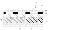
- FIG. 1 is a conceptual cross-sectional view showing an example of an active matrix liquid crystal display device 10.
- the color liquid crystal display device 10 is a liquid crystal panel having a backlight unit 12 on the back surface, and the liquid crystal panel includes all pixels disposed between two glass substrates 14 and 15 having a polarizing film attached thereto.
- the elements of the TFT 16 corresponding to are arranged.
- Each element formed on the glass substrate is wired with an ITO transparent electrode 19 that forms a pixel electrode through a contact hole 18 formed in the cured film 17.
- an RGB color filter 22 in which a liquid crystal 20 layer and a black matrix are arranged is provided.
- the light source of the backlight is not particularly limited, and a known light source can be used.
- the liquid crystal display device can be a 3D (stereoscopic) type or a touch panel type. Further, it can be made flexible, and can be used as the second interphase insulating film (48) of JP 2011-145686 A or the interphase insulating film (520) of JP 2009-258758 A.
- the organic EL display device of the present invention comprises the cured film of the present invention.
- the organic EL display device of the present invention is not particularly limited except that it has a flattening film and an interlayer insulating film formed using the photosensitive resin composition of the present invention, and various known structures having various structures. Examples thereof include an organic EL display device and a liquid crystal display device.
- specific examples of TFT (Thin-Film Transistor) included in the organic EL display device of the present invention include amorphous silicon-TFT, low-temperature polysilicon-TFT, oxide semiconductor TFT, and the like. Since the cured film of the present invention is excellent in electrical characteristics, it can be preferably used in combination with these TFTs.
- FIG. 2 is a conceptual diagram of an example of an organic EL display device.
- a schematic cross-sectional view of a substrate in a bottom emission type organic EL display device is shown, and a planarizing film 4 is provided.
- a bottom gate type TFT 1 is formed on a glass substrate 6, and an insulating film 3 made of Si 3 N 4 is formed so as to cover the TFT 1.
- a contact hole (not shown) is formed in the insulating film 3, and then a wiring 2 (height: 1.0 ⁇ m) connected to the TFT 1 through the contact hole is formed on the insulating film 3.
- the wiring 2 is for connecting the TFT 1 with an organic EL element formed between the TFTs 1 or in a later process.
- the flattening layer 4 is formed on the insulating film 3 in a state where the unevenness due to the wiring 2 is embedded.
- a bottom emission type organic EL element is formed on the planarizing film 4. That is, the first electrode 5 made of ITO is formed on the planarizing film 4 so as to be connected to the wiring 2 through the contact hole 7.
- the first electrode 5 corresponds to the anode of the organic EL element.
- An insulating film 8 having a shape covering the periphery of the first electrode 5 is formed. By providing the insulating film 8, a short circuit between the first electrode 5 and the second electrode formed in the subsequent process is prevented. can do. Further, although not shown in FIG.
- a hole transport layer, an organic light emitting layer, and an electron transport layer are sequentially deposited through a desired pattern mask, and then a second layer made of Al is formed on the entire surface above the substrate.
- An active matrix organic material in which two electrodes are formed and sealed by bonding using a sealing glass plate and an ultraviolet curable epoxy resin, and each organic EL element is connected to a TFT 1 for driving it.
- An EL display device is obtained.
- a resist pattern formed using the photosensitive resin composition of the present invention as a structural member of a MEMS device can be used as a partition wall or mechanically driven. Used as part of the part.
- MEMS devices include parts such as SAW filters, BAW filters, gyro sensors, display micro shutters, image sensors, electronic paper, inkjet heads, biochips, sealants, and the like. More specific examples are exemplified in JP-T-2007-522531, JP-A-2008-250200, JP-A-2009-263544, and the like.
- the photosensitive resin composition of the present invention is excellent in flatness and transparency, for example, the bank layer (16) and the planarization film (57) described in FIG. 2 of JP-A-2011-107476, JP-A-2010-
- MAEVE 1-ethoxyethyl methacrylate
- MATHF tetrahydro-2H-furan-2-yl methacrylate
- PHS parahydroxystyrene
- MAA methacrylic acid (manufactured by Wako Pure Chemical Industries, Ltd.)
- HEMA Hydroxyethyl methacrylate (Wako Pure Chemical Industries, Ltd.)
- EDM (diethylene glycol ethyl methyl ether) (manufactured by Toho Chemical Industry Co., Ltd.)
- BzMA (benzyl methacrylate) (manufactured by Wako Pure Chemical Industries, Ltd.)
- polymer 1 which is an alkali-soluble resin protected with an acid-decomposable group. It was.
- the weight average molecular weight of the obtained resin was 11,000.
- the polydispersity was 1.13.
- the structure of the polymer 1 is a 1-ethoxyethyl protected body of p-hydroxystyrene / p-hydroxystyrene copolymer (30 mol% / 70 mol%).
- polymer 2 which is a soluble resin having a protection rate of 25 mol%.
- the weight average molecular weight of the obtained resin was 12,000.
- the polydispersity was 1.13.
- the structure of the polymer 2 is a 2-tetrahydrofuranyl protected product of p-hydroxystyrene / p-hydroxystyrene copolymer (30 mol% / 70 mol%).
- Polymer 3 was synthesized as follows. To 144.2 parts (2 molar equivalents) of ethyl vinyl ether, 0.5 part of phenothiazine was added, and 86.1 parts (1 molar equivalent) of methacrylic acid was added dropwise while cooling the reaction system to 10 ° C. or lower. ) For 4 hours. After adding 5.0 parts of pyridinium p-toluenesulfonate, the mixture was stirred at room temperature for 2 hours and allowed to stand overnight at room temperature. To the reaction solution, 5 parts of sodium bicarbonate and 5 parts of sodium sulfate were added, and the mixture was stirred at room temperature for 1 hour.
- polymer 4 was also synthesized.
- PAG-1 Synthesized according to the method described in paragraph 0108 of JP-T-2002-528451.
- the Ts portion represents a tosyl group.
- PGMEA Methoxypropyl acetate (manufactured by Showa Denko)
- PGDA 1,2-propanediol diacetate (boiling point 190 ° C., manufacturer: manufactured by Daicel Corporation, product number: PGDA)
- 1,3-BGDA 1,3-butanediol diacetate (boiling point 232 ° C., manufacturer: manufactured by Daicel Corporation, product number: 1,3-BGDA)
- 1,6-HDDA 1,6-hexanediol diacetate (boiling point 260 ° C., manufacturer: manufactured by Daicel Corporation, product number: 1,6-HDDA)
- DRA-150 Triacetin (boiling point 260 ° C., manufacturer: manufactured by Daicel Corporation, product number: DRA-150)
- DPNB Dipropylene glycol-n-butyl ether (boiling point 229 ° C., manufacturer: manufactured by Daicel Corporation
- ⁇ Evaluation of sensitivity> The film was coated on a cleaned and HMDS-treated glass substrate with a film thickness of 1.3 ⁇ m, exposed and developed through a mask, and the sensitivity was evaluated with the exposure amount at which the 10 ⁇ m line-and-space pattern was just 10 ⁇ m as the optimum exposure amount. Three or more are practical levels.
- An exposure amount of 100 mJ / cm 2 or more is required 2: An exposure amount of 50 mJ / cm 2 or more and less than 100 mJ / cm 2 is required 3: An exposure amount of 20 mJ / cm 2 or more and less than 50 mJ / cm 2 is required 4:10 mJ / Exposure amount of cm 2 or more and less than 20 mJ 5: Exposure amount of less than 10 mJ / cm 2
- Standard deviation ⁇ is 0.4 ⁇ m or more 2: Standard deviation ⁇ is 0.2 ⁇ m or more and less than 0.4 ⁇ m 3: Standard deviation ⁇ is 0.15 ⁇ m or more and less than 0.25 ⁇ m 4: Standard deviation ⁇ is 0.1 ⁇ m or more , Less than 0.15 ⁇ m 5: standard deviation ⁇ is less than 0.1 ⁇ m
- Resolution is 5 ⁇ m or more 2: 3.0 ⁇ m is resolved, but 2.5 ⁇ m is not resolved 3: 2.5 ⁇ m is resolved but 2.0 ⁇ m is not resolved 4: 2.0 ⁇ m is resolved 1.5 ⁇ m does not resolve 5: 1.5 ⁇ m resolves.
- a hot plate is applied to a substrate formed by applying a 1.3 ⁇ m film thickness to a glass substrate that has been cleaned and treated with HMDS, and exposing and developing a 10 ⁇ m line-and-space pattern at a dose of exactly 10 ⁇ m through a mask.
- PostBake was performed at a temperature of 140 ° C. for 3 minutes, and the taper angle of a 3 ⁇ m L & S pixel was measured to make it rectangular. Three or more are practical levels.
- the taper angle is less than 30 ° 2: The taper angle is 30 ° or more and less than 45 ° 3: The taper angle is 45 ° or more and less than 60 ° 4: The taper angle is 60 ° or more and less than 75 ° 5: The taper angle is 75 ° or more
- the photosensitive resin composition of each example is excellent in any evaluation of sensitivity, resolution, and rectangularity in comparison with the photosensitive resin composition of each comparative example. It was found that the results were obtained.
- Example 16 An organic EL display device having an ITO pattern was produced by the following method (see FIG. 1).
- a bottom gate type TFT 1 was formed on a glass substrate 6, and an insulating film 3 made of Si 3 N 4 was formed so as to cover the TFT 1.
- a contact hole (not shown) is formed in the insulating film 3, and then a wiring 2 (height 1.0 ⁇ m) connected to the TFT 1 through the contact hole is formed on the insulating film 3. .
- the wiring 2 is used to connect the TFT 1 with an organic EL element formed between TFTs 1 or in a later process.
- the planarizing film 4 was formed on the insulating film 3 in a state where the unevenness due to the wiring 2 was embedded.
- the planarization film 4 is formed on the insulating film 3 by spin-coating the photosensitive resin composition described in Example 1 of JP-A-2009-98616 on a substrate and pre-baking (90 ° C. ⁇ 90 ° C.) on a hot plate.
- a bottom emission type organic EL element was formed on the obtained planarization film 4.
- a first electrode 5 made of ITO was formed on the planarizing film 4 so as to be connected to the wiring 2 through the contact hole 7.
- the photosensitive resin composition of Example 1 was spin-coated on an ITO substrate, pre-baked on a hot plate (90 ° C. ⁇ 2 minutes), and then i-line (365 nm) was 20 mJ from above the mask using a high-pressure mercury lamp. After irradiation with / cm 2 (illuminance 20 mW / cm 2 ), the pattern was formed by developing with an alkaline aqueous solution.
- the post-baking heat processing for 3 minutes were performed at 140 degreeC before the etching process.
- ITO was patterned by wet etching by dipping in an ITO etchant (3% aqueous oxalic acid solution) at 40 ° C./1 min. Thereafter, the resist pattern was peeled off by being immersed in a resist stripping solution (MS2001, manufactured by Fuji Film Electronics Materials Co., Ltd.) at 70 ° C. for 7 minutes.
- the first electrode 5 thus obtained corresponds to the anode of the organic EL element.
- an insulating film 8 having a shape covering the periphery of the first electrode 5 was formed.
- the photosensitive resin composition described in Example 1 of JP2009-98616A was used, and the insulating film 8 was formed by the same method as described above. By providing this insulating film 8, it is possible to prevent a short circuit between the first electrode 5 and the second electrode formed in the subsequent process.
- a hole transport layer, an organic light emitting layer, and an electron transport layer were sequentially deposited through a desired pattern mask in a vacuum deposition apparatus.
- a second electrode made of Al was formed on the entire surface above the substrate.
- substrate was taken out from the vapor deposition machine, and it sealed by bonding together using the glass plate for sealing, and an ultraviolet curable epoxy resin.
- an organic EL display device having an active matrix type ITO pattern formed by connecting each organic EL element to TFT 1 for driving the organic EL element was obtained.
- a voltage was applied via the drive circuit, it was found that the organic EL display device showed good display characteristics and high reliability.
- Example 17 A liquid crystal display device having an ITO pattern was produced by the following method.
- the pixel electrode 4 was formed using the photosensitive resin composition of Example 1 as a mask, and the liquid crystal display device of Example 17 was obtained. That is, the pixel electrode 4 was formed by the same method as the method for forming the first electrode 5 of the organic EL display device in Example 16.
- TFT Thin Film Transistor
- Wiring 3 Insulating film 4: Flattened film 5: First electrode 6: Glass substrate 7: Contact hole 8: Insulating film 10: Liquid crystal display device 12: Backlight unit 14, 15: Glass substrate 16: TFT 17: Cured film 18: Contact hole 19: ITO transparent electrode 20: Liquid crystal 22: Color filter
Landscapes
- Chemical & Material Sciences (AREA)
- Physics & Mathematics (AREA)
- Health & Medical Sciences (AREA)
- Chemical Kinetics & Catalysis (AREA)
- Medicinal Chemistry (AREA)
- Polymers & Plastics (AREA)
- Organic Chemistry (AREA)
- Spectroscopy & Molecular Physics (AREA)
- General Physics & Mathematics (AREA)
- Manufacturing & Machinery (AREA)
- Engineering & Computer Science (AREA)
- Emergency Medicine (AREA)
- Materials For Photolithography (AREA)
- Electroluminescent Light Sources (AREA)
- Addition Polymer Or Copolymer, Post-Treatments, Or Chemical Modifications (AREA)
- Exposure And Positioning Against Photoresist Photosensitive Materials (AREA)
Description
<1>(A1)下記一般式(1)で表される構成単位(a1)を有する重合体を含む重合体成分、
(B)光酸発生剤、
(C)脂環式エポキシ化合物、および
(D1)分子内にアセテート構造を2つ以上含有する溶剤、
を含有する感光性樹脂組成物。
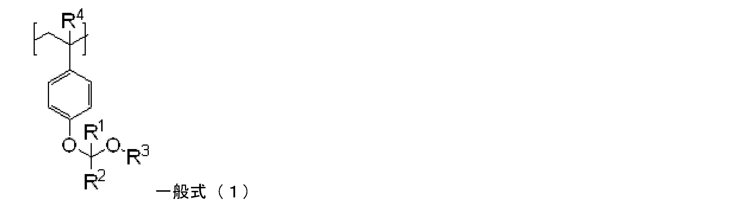
<2>前記(C)脂環式エポキシ化合物が、下記一般式(I)で表される化合物である、<1>に記載の感光性樹脂組成物。

<3>前記一般式(I)で表される化合物中のnが1または2である、<2>に記載の感光性樹脂組成物。
<4>さらに、(A2)酸分解性基で保護された保護カルボキシル基を有する構成単位(a4)を有する重合体成分を含む、<1>~<3>のいずれかに記載の感光性樹脂組成物。
<5>前記構成単位(a4)が、下記一般式(A2’)で表される構成単位である、<4>に記載の感光性樹脂組成物。
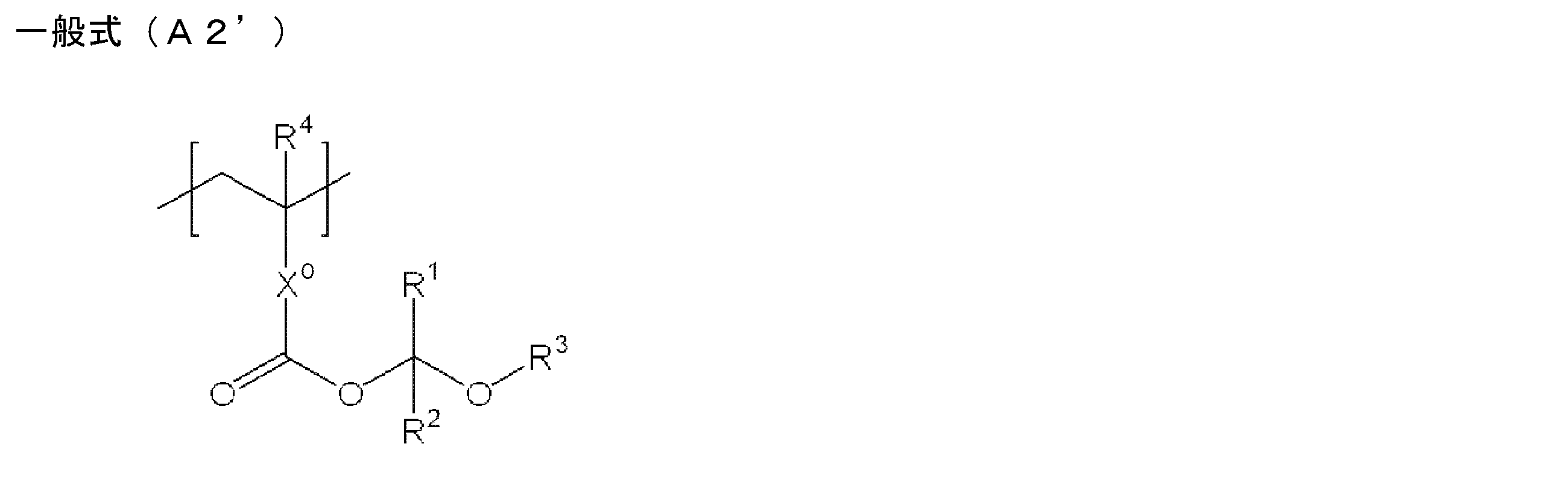
<6>前記(C)脂環式エポキシ化合物の含有量が、全固形分量に対して0.05~5質量%である、<1>~<5>のいずれかに記載の感光性樹脂組成物。
<7>前記(D1)分子内にアセテート構造を2つ以上含有する溶剤と、(D1)分子内にアセテート構造を2つ以上含有する溶剤と異なる他の溶剤(D2)とを含む、<1>~<6>のいずれかに記載の感光性樹脂組成物。
<8>前記(D1)分子内にアセテート構造を2つ以上含有する溶剤の沸点が、130℃以上300℃未満である、<1>~<7>のいずれかに記載の感光性樹脂組成物。
<9>前記(D1)分子内にアセテート構造を2つ以上含有する溶剤の含有量が、前記感光性樹脂組成物の1~10質量%である、<1>~<8>のいずれかに記載の感光性樹脂組成物。
<10>(1)基板の少なくとも一方の面に、<1>~<9>のいずれかに記載の感光性樹脂組成物を塗布する工程、
(2)乾燥により有機溶剤を揮発させ、感光性樹脂組成物層を形成する工程、
(3)前記感光性樹脂組成物層を露光する工程、
(4)露光された前記感光性樹脂組成物層を現像する工程、を含むパターンの製造方法。
<11>形成されたパターンをエッチング用レジストとして用いてエッチングを行う工程、および前記パターンをプラズマ処理または薬品処理により除去する工程、を含む、<10>に記載のパターンの製造方法。
<12><1>~<9>のいずれかに記載の感光性樹脂組成物を硬化させてなる硬化膜。
<13><10>または<11>に記載のパターンの製造方法を含む、有機EL表示装置または液晶表示装置の製造方法。
さらに、(メタ)アクリル酸とは、アクリル酸および/またはメタクリル酸を意味する。
(A1)下記一般式(1)で表される構成単位(a1)を有する重合体を含む重合体成分、
(B)光酸発生剤、
(C)脂環式エポキシ化合物、および
(D1)分子内にアセテート構造を2つ以上含有する溶剤、
を含有することを特徴とする。
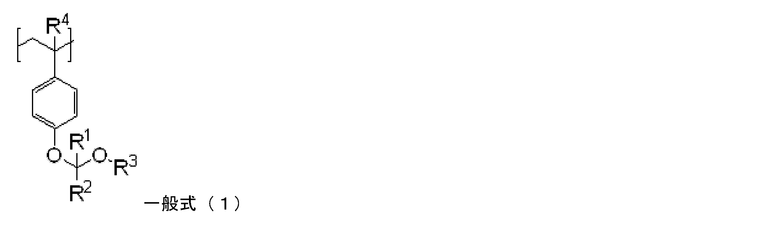
本発明の感光性樹脂組成物は、化学増幅型ポジ型感光性樹脂組成物として好ましく用いられる。
以下、本発明の組成物について詳細に説明する。
本発明の感光性樹脂組成物は、重合体成分(A)として、(A1)下記一般式(1)で表される構成単位(a1)を有する重合体成分を含む。(A1)重合体成分は、一般式(1)で表される構成単位(a1)以外の重合体を含んでいてもよい。また、重合体成分は、(A2)酸分解性基で保護された保護カルボキシル基を有する構成単位(a4)を有することが好ましい。
以下、これらの重合体成分について説明する。
本発明における(A1)重合体成分は、一般式(1)で表される構成単位(a1)を有する重合体を含む重合体成分である。(A1)成分が構成単位(a1)を有することにより解像力および矩形性に優れる感光性樹脂組成物とすることができる。
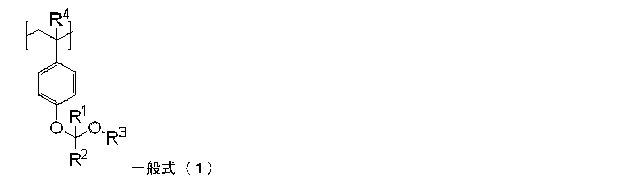
アルキル基としては、炭素数1~10のアルキル基が好ましく、炭素数1~8のアルキル基がより好ましく、炭素数1~6のアルキル基がさらに好ましい。アルキル基は、置換基を有していてもよい。また、アルキル基は、直鎖、分岐、環状のいずれであってもよいが、直鎖のアルキル基が好ましい。アルキル基としては、例えば、メチル基、エチル基、プロピル基、ブチル基、t-ブチル基、ペンチル基、ヘキシル基、シクロヘキシル基等が例示される。
アリール基としては、炭素数6~20のアリール基が好ましく、炭素数6~14のアリール基がより好ましく、炭素数6~10のアリール基がさらに好ましい。アリール基は、置換基を有していてもよい。アリール基としては、例えば、フェニル基、ナフチル基、アントラセニル基等が例示される。


OH基は、p-、m-、o-のいずれでもよいが、p位に結合していることが好ましい。
本発明の感光性樹脂組成物は、(A1)重合体成分の他に(A2)重合体成分を含んでいてもよい。(A2)酸分解性基で保護された保護カルボキシル基を有する構成単位(a4)を有する重合体成分が好ましい。ここで、酸分解性基とは酸の存在下で分解することが可能な官能基を意味する。
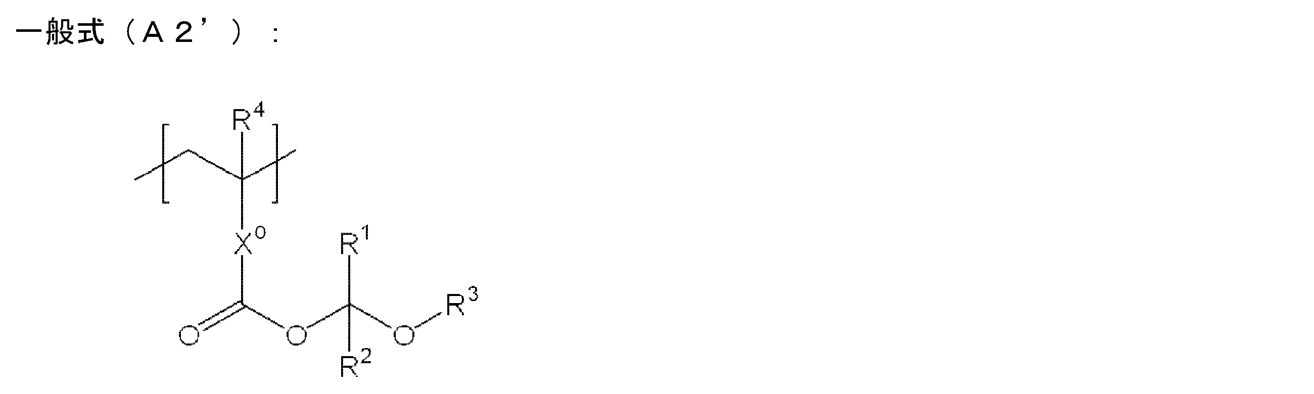
R3は、アルキル基またはアリール基を表し、炭素数1~10のアルキル基が好ましく、1~6のアルキル基がより好ましい。
X0は単結合またはアリーレン基を表し、単結合が好ましい。

本発明の感光性樹脂組成物は、重合体成分として、(A1)と(A2)を含むことが好ましい。これらの質量比は、1:6~6:1が好ましく、2:5~8:1がさらに好ましい。このような範囲とすることにより、本発明の効果がより効果的に発揮される傾向にある。
本発明において、(A)成分は、上記構成単位(a1)、(a2)および(a4)に加えて、これら以外の他の構成単位(a3)を有していてもよい。これらの構成単位は、上記重合体成分(A1)および(A2)のいずれか一方が含んでいても良く、両方が含んでいてもよい。また、上記重合体成分(A1)または(A2)とは別に、実質的に(a1)、(a2)および(a4)を含まずに他の構成単位(a3)を有する重合体成分(A3)を有していてもよい。上記重合体成分(A1)または(A2)とは別に、実質的に(a1)、(a2)および(a4)を含まずに他の構成単位(a3)を有する重合体成分を含む場合、該重合体成分の配合量は、全重合体成分中、60質量%以下であることが好ましく、40質量%以下であることがより好ましく、20質量%以下であることがさらに好ましい。
本発明の感光性樹脂組成物は、(B)光酸発生剤を含有する。本発明で使用される光酸発生剤(「(B)成分」ともいう。)としては、波長300nm以上、好ましくは波長300~450nmの活性光線に感応し、酸を発生する化合物が好ましいが、その化学構造に制限されるものではない。また、波長300nm以上の活性光線に直接感応しない光酸発生剤についても、増感剤と併用することによって波長300nm以上の活性光線に感応し、酸を発生する化合物であれば、増感剤と組み合わせて好ましく用いることができる。本発明で使用される光酸発生剤としては、pKaが4以下の酸を発生する光酸発生剤が好ましく、pKaが3以下の酸を発生する光酸発生剤がより好ましく、2以下の酸を発生する光酸発生剤が最も好ましい。
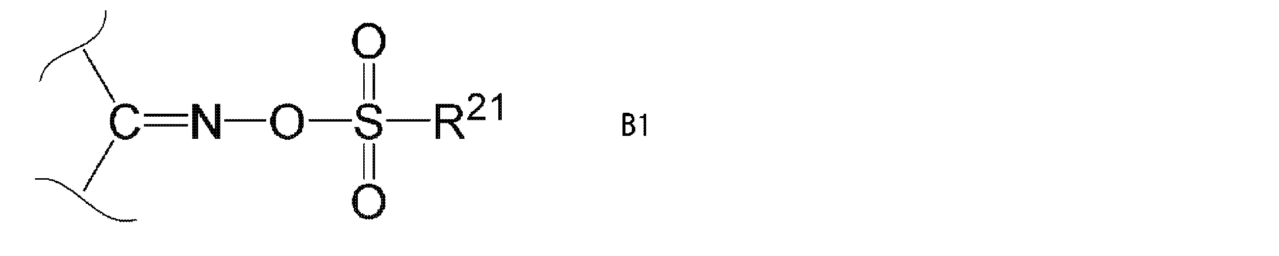
R21のアルキル基としては、炭素数1~10の、直鎖状または分岐状アルキル基が好ましい。R21のアルキル基は、炭素数6~11のアリール基、炭素数1~10のアルコキシ基、または、シクロアルキル基(7,7-ジメチル-2-オキソノルボルニル基などの有橋式脂環基を含む、好ましくはビシクロアルキル基等)で置換されてもよい。
R21のアリール基としては、炭素数6~11のアリール基が好ましく、フェニル基またはナフチル基がより好ましい。R21のアリール基は、低級アルキル基、アルコキシ基あるいはハロゲン原子で置換されてもよい。

Xとしてのアルコキシ基は、炭素数1~4の直鎖状または分岐状アルコキシ基が好ましい。
Xとしてのハロゲン原子は、塩素原子またはフッ素原子が好ましい。 m4は、0または1が好ましい。上記一般式(B2)中、m4が1であり、Xがメチル基であり、Xの置換位置がオルト位であり、R42が炭素数1~10の直鎖状アルキル基、7,7-ジメチル-2-オキソノルボルニルメチル基、またはp-トルイル基である化合物が特に好ましい。
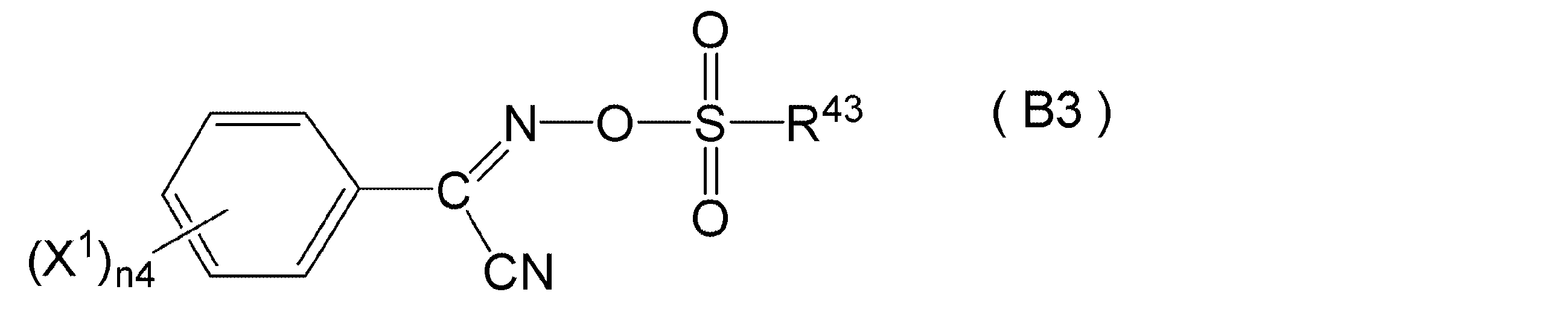
X1としては、炭素数1~5のアルコキシ基が好ましく、メトキシ基がより好ましい。
n4としては、0~2が好ましく、0~1が特に好ましい。

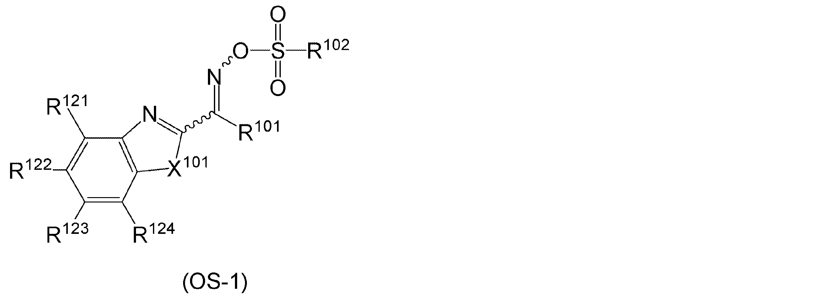
X101は-O-、-S-、-NH-、-NR105-、-CH2-、-CR106H-、または、-CR105R107-を表し、R105~R107はアルキル基、または、アリール基を表す。
R121~R124は、それぞれ独立に、水素原子、ハロゲン原子、アルキル基、アルケニル基、アルコキシ基、アミノ基、アルコキシカルボニル基、アルキルカルボニル基、アリールカルボニル基、アミド基、スルホ基、シアノ基、または、アリール基を表す。R121~R124のうち2つは、それぞれ互いに結合して環を形成してもよい。
R121~R124としては、水素原子、ハロゲン原子、および、アルキル基が好ましく、また、R121~R124のうち少なくとも2つが互いに結合してアリール基を形成する態様もまた、好ましく挙げられる。中でも、R121~R124がいずれも水素原子である態様が感度の観点から好ましい。
既述の官能基は、いずれも、さらに置換基を有していてもよい。
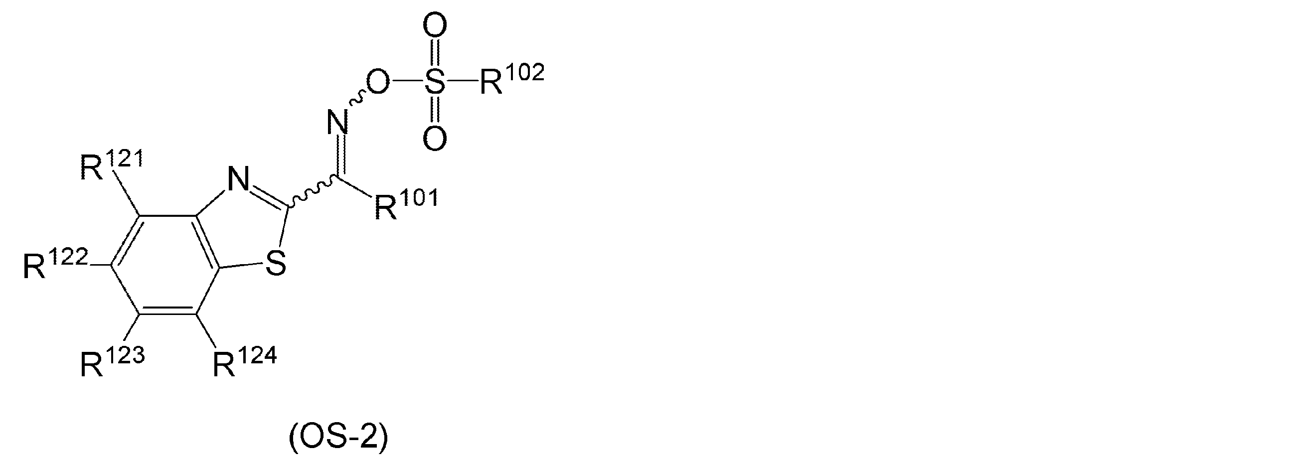
これらの中でも、上記一般式(OS-1)および上記一般式(OS-2)におけるR101がシアノ基、または、アリール基である態様がより好ましく、上記一般式(OS-2)で表され、R101がシアノ基、フェニル基またはナフチル基である態様が最も好ましい。

上記式(OS-3)~(OS-5)中、R22、R25およびR28におけるアルキル基としては、置換基を有していてもよい総炭素数1~30のアルキル基であることが好ましい。
上記一般式(OS-3)~(OS-5)中、化合物中に2以上存在するR23、R26およびR29のうち、1つまたは2つがアルキル基、アリール基またはハロゲン原子であることが好ましく、1つがアルキル基、アリール基またはハロゲン原子であることがより好ましく、1つがアルキル基であり、かつ残りが水素原子であることが特に好ましい。
上記一般式(OS-3)~(OS-5)において、X1~X3を環員として含む環は、5員環または6員環である。
上記一般式(OS-3)~(OS-5)中、n1~n3はそれぞれ独立に1または2を表し、X1~X3がOである場合、n1~n3はそれぞれ独立に1であることが好ましく、また、X1~X3がSである場合、n1~n3はそれぞれ独立に2であることが好ましい。
R24、R27およびR30におけるアルキル基、アルキルオキシ基、スルホン酸基、アミノスルホニル基およびアルコキシスルホニル基は、置換基を有していてもよい。
上記一般式(OS-3)~(OS-5)中、R24、R27およびR30におけるアルキル基としては、置換基を有していてもよい総炭素数1~30のアルキル基であることが好ましい。
また、上記(OS-3)~(OS-5)のそれぞれの置換基について、特開2011-221494号公報の段落番号0092~0109に記載の(OS-3)~(OS-5)の置換基の好ましい範囲も同様に好ましい。
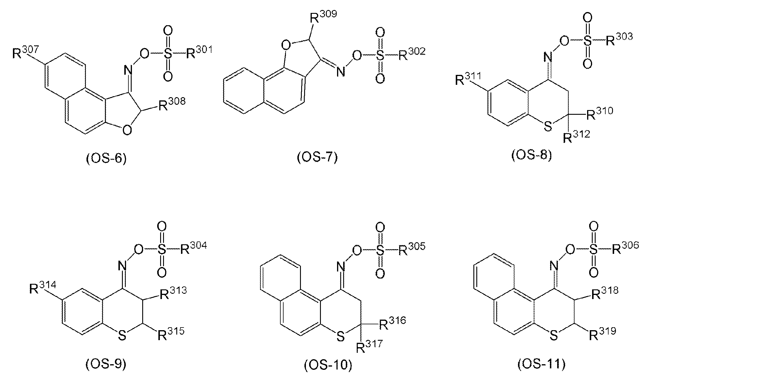
本発明の感光性樹脂組成物は、架橋剤として脂環式エポキシ化合物を含有する。脂環式エポキシ化合物は、酸発生剤による酸を素早くトラップするため、かかる化合物を配合することにより、感度、線幅安定性、解像性および矩形性に優れた感光性樹脂組成物となると考えられる。
本発明で用いる脂環式エポキシ化合物が有する脂環式エポキシ基としては、特に限定されず、例えば環状脂肪族炭化水素に直接付加した脂環式エポキシ基などが例示され、環状脂肪族炭化水素としては、3~10員環が好ましく、5~6員環がより好ましい。中でも、好ましくは下記で表される脂環式エポキシ基である。



R2は炭素数1~15の有機基を表し、分岐していても不飽和結合を有していてもよく、脂肪族環または芳香環の環状構造を有してもよい。また、これらの基は、酸素、硫黄、窒素、リン、ホウ素、ハロゲン原子を有していてもよい。また、置換基を有していてもよく、置換基同士が互いに結合を形成していても良い。また、R2は2価の連結基である。

R3は炭素数1~15の有機基を表し、分岐していても不飽和結合を有していてもよく、脂肪族環または芳香環の環状構造を有してもよい。また、これらの基は、酸素、硫黄、窒素、リン、ホウ素、ハロゲン原子を有していてもよい。また、置換基を有していてもよく、置換基同士が互いに結合を形成していても良い。また、R3は2価の連結基である。

本発明の感光性樹脂組成物は、(D)溶剤として、(D1)分子内にアセテート構造を2つ以上含有する溶剤を含有する。メカニズムは定かではないが、このような溶媒を配合することにより、適度な塗膜の可塑剤になり、また、クエンチャーと脂環エポキシ化合物よる酸の適度な捕捉を促進することにより、感度、線幅安定性、解像性および矩形性が向上させることが可能になると推定される。本発明の感光性樹脂組成物は、本発明の必須成分と、さらに後述の任意の成分を(D1)溶剤に溶解した溶液として調製されることが好ましい。
また、(D1)分子内にアセテート構造を2つ以上含有する溶剤は、沸点が130℃以上300℃未満の溶剤が好ましく、180℃以上270℃未満の溶剤が好ましく、200℃以上270℃未満のものがより好ましい。なお、沸点は、特に断りがない限り1気圧における沸点である。また、溶剤を2種類以上含む溶媒混合の場合、沸点は、全溶媒に対する各溶媒の沸点をそれぞれの重量割合にて加重平均したものとする。
沸点160℃以上の溶剤としては、3-エトキシプロピオン酸エチル(沸点170℃)、ジエチレングリコールメチルエチルエーテル(沸点176℃)、プロピレングリコールモノメチルエーテルプロピオネート(沸点160℃)、ジプロピレングリコールメチルエーテルアセテート(沸点213℃)、3-メトキシブチルエーテルアセテート(沸点171℃)、ジエチレングリコールジエチエルエーテル(沸点189℃)、ジエチレングリコールジメチルエーテル(沸点162℃)、ジエチレングリコールモノエチルエーテルアセテート(沸点220℃)、ジプロピレングリコールジメチルエーテル(沸点175℃)が例示できる。
本発明の感光性樹脂組成物には、上記成分に加えて、必要に応じて、(E)アルコキシシラン化合物、(F)架橋剤、(G)増感剤、(H)塩基性化合物、(I)界面活性剤、(J)酸化防止剤、を好ましく加えることができる。さらに本発明の感光性樹脂組成物には、酸増殖剤、現像促進剤、可塑剤、熱ラジカル発生剤、熱酸発生剤、紫外線吸収剤、増粘剤、および、有機または無機の沈殿防止剤などの公知の添加剤を加えることができる。
本発明の感光性樹脂組成物は、(E)アルコキシシラン化合物(「(E)成分」ともいう)を含有することを特徴とする。アルコキシシラン化合物を用いると、本発明の感光性樹脂組成物により形成された膜と基板との密着性を向上できたり、本発明の感光性樹脂組成物により形成された膜の性質を調整することができる。アルコキシシラン化合物としては、ジアルコキシシラン化合物またはトリアルコキシシラン化合物が好ましく、トリアルコキシシラン化合物がより好ましい。アルコキシシラン化合物が有するアルコキシ基の炭素数は1~5が好ましい。
本発明の感光性樹脂組成物に用いることができる(E)アルコキシシラン化合物は、基材となる無機物、例えば、シリコン、酸化シリコン、窒化シリコン等のシリコン化合物、金、銅、モリブデン、チタン、アルミニウム等の金属と絶縁膜との密着性を向上させる化合物であることが好ましい。具体的には、公知のシランカップリング剤等も有効である。
シランカップリング剤としては、例えば、γ-アミノプロピルトリメトキシシラン、γ-アミノプロピルトリエトキシシラン、γ-グリシドキシプロピルトリアルコキシシラン、γ-グリシドキシプロピルアルキルジアルコキシシラン、γ-メタクリロキシプロピルトリアルコキシシラン、γ-メタクリロキシプロピルアルキルジアルコキシシラン、γ-クロロプロピルトリアルコキシシラン、γ-メルカプトプロピルトリアルコキシシラン、β-(3,4-エポキシシクロヘキシル)エチルトリアルコキシシラン、ビニルトリアルコキシシランが挙げられる。これらのうち、γ-グリシドキシプロピルトリアルコキシシランやγ-メタクリロキシプロピルトリアルコキシシランがより好ましく、γ-グリシドキシプロピルトリアルコキシシランがさらに好ましく、3-グリシドキシプロピルトリメトキシシランがよりさらに好ましい。これらは1種単独または2種以上を組み合わせて使用することができる。
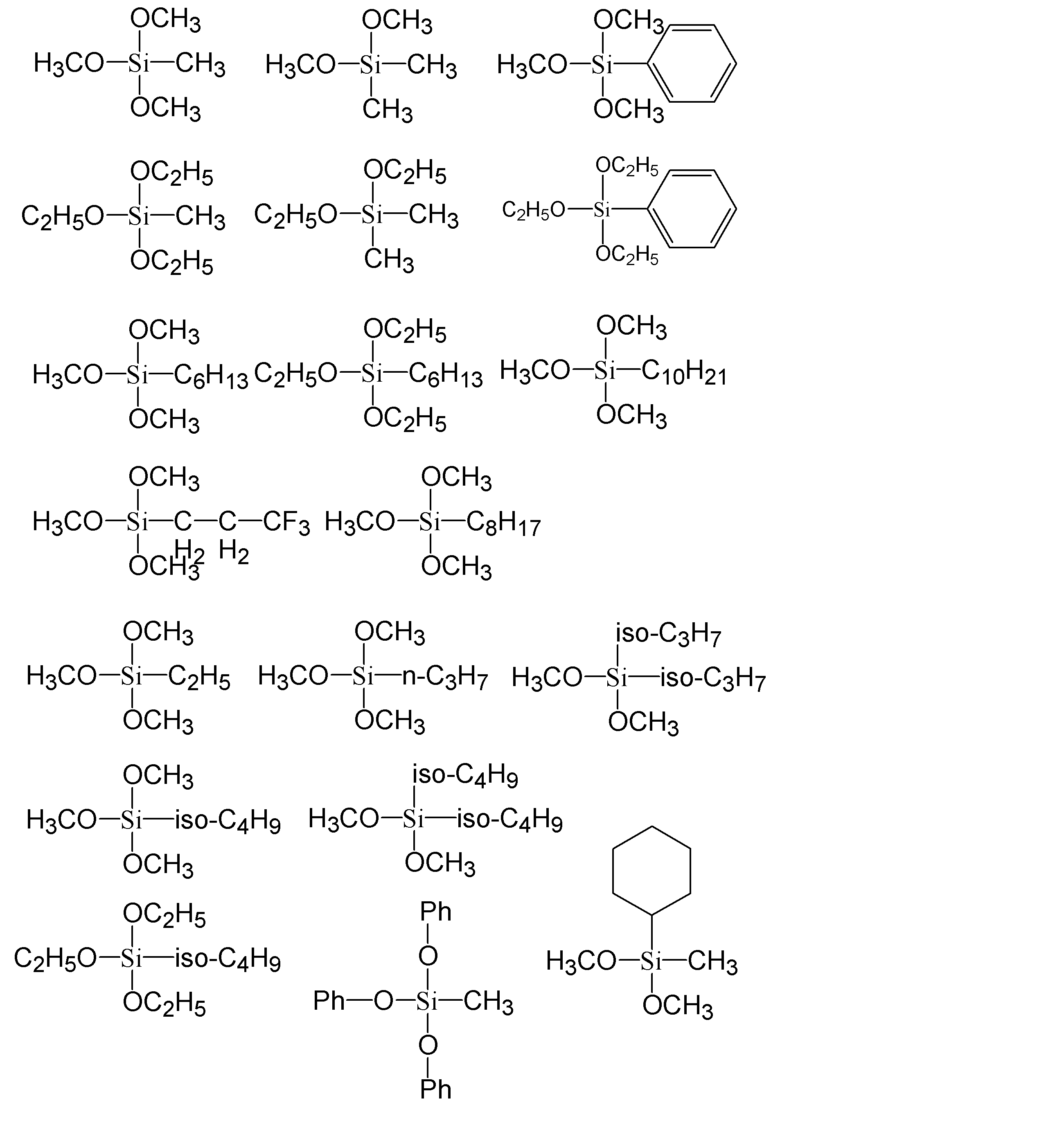
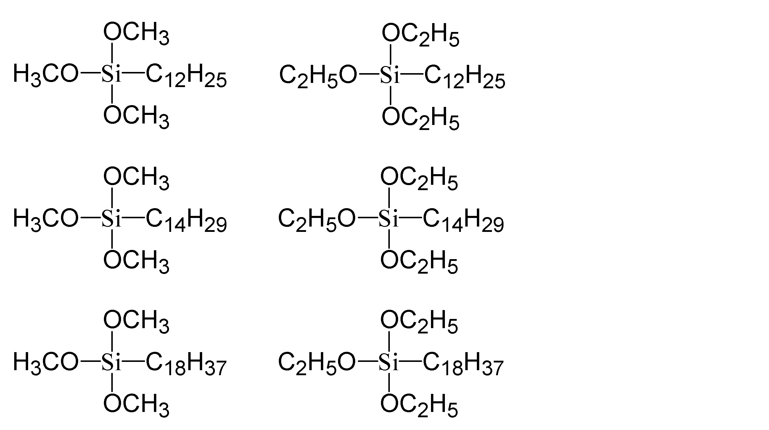
本発明の感光性樹脂組成物における(E)アルコキシシラン化合物の含有量は、感光性組成物中の全固形分100質量部に対して、0.1~30質量部が好ましく、0.5~20質量部がより好ましい。
本発明の感光性樹脂組成物は、必要に応じ、架橋剤を含有することが好ましい。架橋剤を添加することにより、本発明の感光性樹脂組成物により得られる硬化膜をより強固な膜とすることができる。
架橋剤としては、熱によって架橋反応が起こるものであれば制限は無い。(A成分を除く)。例えば、以下に述べる分子内に2個以上のエポキシ基またはオキセタニル基を有する化合物、アルコキシメチル基含有架橋剤、または、少なくとも1個のエチレン性不飽和二重結合を有する化合物、ブロックイソシアネート化合物等を添加することができる。
本発明の感光性樹脂組成物中における架橋剤の添加量は、感光性樹脂組成物の全固形分100質量部に対し、0.01~50質量部であることが好ましく、0.1~30質量部であることがより好ましく、0.5~20質量部であることがさらに好ましい。この範囲で添加することにより、機械的強度および耐溶剤性に優れた硬化膜が得られる。架橋剤は複数を併用することもでき、その場合は架橋剤を全て合算して含有量を計算する。
分子内に2個以上のエポキシ基を有する化合物の具体例としては、ビスフェノールA型エポキシ樹脂、ビスフェノールF型エポキシ樹脂、フェノールノボラック型エポキシ樹脂、クレゾールノボラック型エポキシ樹脂、脂肪族エポキシ樹脂等を挙げることができる。
その他にも、ADEKA RESIN EP-4000S、同EP-4003S、同EP-4010S、同EP-4011S(以上、(株)ADEKA製)、NC-2000、NC-3000、NC-7300、XD-1000、EPPN-501、EPPN-502(以上、(株)ADEKA製)、デナコールEX-611、EX-612、EX-614、EX-614B、EX-622、EX-512、EX-521、EX-411、EX-421、EX-313、EX-314、EX-321、EX-211、EX-212、EX-810、EX-811、EX-850、EX-851、EX-821、EX-830、EX-832、EX-841、EX-911、EX-941、EX-920、EX-931、EX-212L、EX-214L、EX-216L、EX-321L、EX-850L、DLC-201、DLC-203、DLC-204、DLC-205、DLC-206、DLC-301、DLC-402(以上ナガセケムテック製)、YH-300、YH-301、YH-302、YH-315、YH-324、YH-325(以上新日鐵化学製)セロキサイド2021P、2081、3000、EHPE3150、エポリードGT400、セルビナースB0134、B0177((株)ダイセル)、などが挙げられる。
これらは1種単独または2種以上を組み合わせて使用することができる。
本発明の感光性樹脂組成物では、架橋剤として、ブロックイソシアネート系化合物も好ましく採用できる。ブロックイソシアネート化合物は、ブロックイソシアネート基を有する化合物であれば特に制限はないが、硬化性の観点から、1分子内に2以上のブロックイソシアネート基を有する化合物であることが好ましい。
なお、本発明におけるブロックイソシアネート基とは、熱によりイソシアネート基を生成することが可能な基であり、例えば、ブロック剤とイソシアネート基とを反応させイソシアネート基を保護した基が好ましく例示できる。また、前記ブロックイソシアネート基は、90℃~250℃の熱によりイソシアネート基を生成することが可能な基であることが好ましい。
また、ブロックイソシアネート化合物としては、その骨格は特に限定されるものではなく、1分子中にイソシアネート基を2個有するものであればどのようなものでもよく、脂肪族、脂環族または芳香族のポリイソシアネートであってよいが、例えば2,4-トリレンジイソシアネート、2,6-トリレンジイソシアネート、イソホロンジイソシアネート、1,6-ヘキサメチレンジイソシアネート、1,3-トリメチレンジイソシアネート、1,4-テトラメチレンジイソシアネート、2,2,4-トリメチルヘキサメチレンジイソシアネート、2,4,4-トリメチルヘキサメチレンジイソシアネート、1,9-ノナメチレンジイソシアネート、1,10-デカメチレンジイソシアネート、1,4-シクロヘキサンジイソシアネート、2,2’-ジエチルエーテルジイソシアネート、ジフェニルメタン-4,4’-ジイソシアネート、o-キシレンジイソシアネート、m-キシレンジイソシアネート、p-キシレンジイソシアネート、メチレンビス(シクロヘキシルイソシアネート)、シクロヘキサン-1,3-ジメチレンジイソシアネート、シクロヘキサン-1,4-ジメチレレンジイソシアネート、1,5-ナフタレンジイソシアネート、p-フェニレンジイソシアネート、3,3’-メチレンジトリレン-4,4’-ジイソシアネート、4,4’-ジフェニルエーテルジイソシアネート、テトラクロロフェニレンジイソシアネート、ノルボルナンジイソシアネート、水素化1,3-キシリレンジイソシアネート、水素化1,4-キシリレンジイソシアネート等のイソシアネート化合物およびこれらの化合物から派生するプレポリマー型の骨格の化合物を好適に用いることができる。これらの中でも、トリレンジイソシアネート(TDI)やジフェニルメタンジイソシアネート(MDI)、ヘキサメチレンジイソシアネート(HDI)、イソホロンジイソシアネート(IPDI)が特に好ましい。
前記ブロックイソシアネート化合物のブロック構造を形成するブロック剤としては、オキシム化合物、ラクタム化合物、フェノール化合物、アルコール化合物、アミン化合物、活性メチレン化合物、ピラゾール化合物、メルカプタン化合物、イミダゾール系化合物、イミド系化合物等を挙げることができる。これらの中でも、オキシム化合物、ラクタム化合物、フェノール化合物、アルコール化合物、アミン化合物、活性メチレン化合物、ピラゾール化合物から選ばれるブロック剤が特に好ましい。
前記ラクタム化合物としてはε-カプロラクタム、γ-ブチロラクタム等が例示できる。
前記フェノール化合物としては、フェノール、ナフトール、クレゾール、キシレノール、ハロゲン置換フェノール等が例示できる。
前記アルコール化合物としては、メタノール、エタノール、プロパノール、ブタノール、シクロヘキサノール、エチレングリコールモノアルキルエーテル、プロピレングリコールモノアルキルエーテル、乳酸アルキル等が例示できる。
前記アミン化合物としては、1級アミンおよび2級アミンが上げられ、芳香族アミン、脂肪族アミン、脂環族アミンいずれでもよく、アニリン、ジフェニルアミン、エチレンイミン、ポリエチレンイミン等が例示できる。
前記活性メチレン化合物としては、マロン酸ジエチル、マロン酸ジメチル、アセト酢酸エチル、アセト酢酸メチル等が例示できる。
前記ピラゾール化合物としては、ピラゾール、メチルピラゾール、ジメチルピラゾール等が例示できる、
前記メルカプタン化合物としては、アルキルメルカプタン、アリールメルカプタン等が例示できる。
本発明の感光性樹脂組成物は、(B)光酸発生剤との組み合わせにおいて、その分解を促進させるために、増感剤を含有することが好ましい。増感剤は、活性光線または放射線を吸収して電子励起状態となる。電子励起状態となった増感剤は、光酸発生剤と接触して、電子移動、エネルギー移動、発熱などの作用が生じる。これにより光酸発生剤は化学変化を起こして分解し、酸を生成する。好ましい増感剤の例としては、以下の化合物類に属しており、かつ350nmから450nmの波長域のいずれかに吸収波長を有する化合物を挙げることができる。
これら増感剤の中でも、多核芳香族類、アクリドン類、スチリル類、ベーススチリル類、クマリン類が好ましく、多核芳香族類がより好ましい。多核芳香族類の中でもアントラセン誘導体が最も好ましい。
2種以上を併用することもできる。
本発明の感光性樹脂組成物は、(H)塩基性化合物を含有してもよい。(H)塩基性化合物としては、化学増幅レジストで用いられるものの中から任意に選択して使用することができる。例えば、脂肪族アミン、芳香族アミン、複素環式アミン、第四級アンモニウムヒドロキシド、カルボン酸の第四級アンモニウム塩等が挙げられる。これらの具体例としては、特開2011-221494号公報の段落番号0204~0207に記載の化合物が挙げられ、これらの内容は本願明細書に組み込まれる。また、N-シクロヘキシル-N’-[2-(4-モルホリニル)エチル]チオ尿素などのチオ尿素類を用いてもよい。
本発明の感光性樹脂組成物は、(I)界面活性剤を含有してもよい。(I)界面活性剤としては、アニオン系、カチオン系、ノニオン系、または、両性のいずれでも使用することができるが、好ましい界面活性剤はノニオン界面活性剤である。
ノニオン系界面活性剤の例としては、ポリオキシエチレン高級アルキルエーテル類、ポリオキシエチレン高級アルキルフェニルエーテル類、ポリオキシエチレングリコールの高級脂肪酸ジエステル類、シリコーン系、フッ素系界面活性剤を挙げることができる。また、以下商品名で、KP(信越化学工業(株)製)、ポリフロー(共栄社化学(株)製)、エフトップ(JEMCO社製)、メガファック(DIC(株)製)、フロラード(住友スリーエム(株)製)、アサヒガード、サーフロン(旭硝子(株)製)、PolyFox(OMNOVA社製)、SH-8400(東レ・ダウコーニングシリコーン)等の各シリーズを挙げることができる。
また、界面活性剤として、下記一般式(I-1)で表される構成単位Aおよび構成単位Bを含み、テトラヒドロフラン(THF)を溶剤とした場合のゲルパーミエーションクロマトグラフィーで測定されるポリスチレン換算の重量平均分子量(Mw)が1,000以上10,000以下である共重合体を好ましい例として挙げることができる。
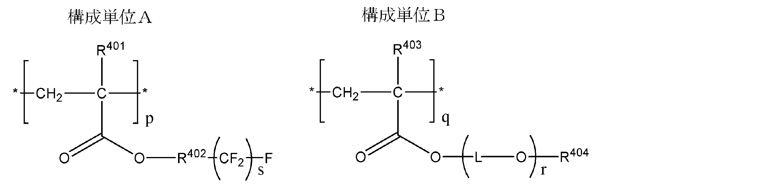

本発明の感光性樹脂組成物における(I)界面活性剤の添加量は、感光性樹脂組成物中の全固形分100質量部に対して、10質量部以下であることが好ましく、0.001~10質量部であることがより好ましく、0.01~3質量部であることがさらに好ましい。
本発明の感光性樹脂組成物は、酸化防止剤を含有してもよい。酸化防止剤としては、公知の酸化防止剤を含有することができる。酸化防止剤を添加することにより、硬化膜の着色を防止できる、または、分解による膜厚減少を低減でき、また、耐熱透明性に優れるという利点がある。
このような酸化防止剤としては、例えば、リン系酸化防止剤、アミド類、ヒドラジド類、ヒンダードアミン系酸化防止剤、イオウ系酸化防止剤、フェノール系酸化防止剤、アスコルビン酸類、硫酸亜鉛、糖類、亜硝酸塩、亜硫酸塩、チオ硫酸塩、ヒドロキシルアミン誘導体などを挙げることができる。これらの中では、硬化膜の着色、膜厚減少の観点から特にフェノール系酸化防止剤、アミド系酸化防止剤、ヒドラジド系酸化防止剤、イオウ系酸化防止剤が好ましい。これらは1種単独で用いてもよいし、2種以上を混合してもよい。
フェノール系酸化防止剤の市販品としては、例えば、アデカスタブAO-15、アデカスタブAO-18、アデカスタブAO-20、アデカスタブAO-23、アデカスタブAO-30、アデカスタブAO-37、アデカスタブAO-40、アデカスタブAO-50、アデカスタブAO-51、アデカスタブAO-60、アデカスタブAO-70、アデカスタブAO-80、アデカスタブAO-330、アデカスタブAO-412S、アデカスタブAO-503、アデカスタブA-611、アデカスタブA-612、アデカスタブA-613、アデカスタブPEP-4C、アデカスタブPEP-8、アデカスタブPEP-8W、アデカスタブPEP-24G、アデカスタブPEP-36、アデカスタブPEP-36Z、アデカスタブHP-10、アデカスタブ2112、アデカスタブ260、アデカスタブ522A、アデカスタブ1178、アデカスタブ1500、アデカスタブC、アデカスタブ135A、アデカスタブ3010、アデカスタブTPP、アデカスタブCDA-1、アデカスタブCDA-6、アデカスタブZS-27、アデカスタブZS-90、アデカスタブZS-91(以上、(株)ADEKA製)、イルガノックス245FF、イルガノックス1010FF、イルガノックス1010、イルガノックスMD1024、イルガノックス1035FF、イルガノックス1035、イルガノックス1098、イルガノックス1330、イルガノックス1520L、イルガノックス3114、イルガノックス1726、イルガフォス168、イルガモッド295(BASF(株)製)などが挙げられる。中でも、アデカスタブAO-60、アデカスタブAO-80、イルガノックス1726、イルガノックス1035、イルガノックス1098を好適に使用することができる。
また、酸化防止剤以外の添加剤として、“高分子添加剤の新展開((株)日刊工業新聞社)”に記載の各種紫外線吸収剤や、金属不活性化剤等を本発明の感光性樹脂組成物に添加してもよい。
本発明の感光性樹脂組成物は、感度向上を目的に、酸増殖剤を用いることができる。
本発明に用いることができる酸増殖剤は、酸触媒反応によってさらに酸を発生して反応系内の酸濃度を上昇させることができる化合物であり、酸が存在しない状態では安定に存在する化合物である。このような化合物は、1回の反応で1つ以上の酸が増えるため、反応の進行に伴って加速的に反応が進むが、発生した酸自体が自己分解を誘起するため、ここで発生する酸の強度は、酸解離定数、pKaとして3以下であるのが好ましく、特に2以下であるのが好ましい。
酸増殖剤の具体例としては、特開平10-1508号公報の段落番号0203~0223、特開平10-282642号公報の段落番号0016~0055、および、特表平9-512498号公報第39頁12行目~第47頁2行目に記載の化合物を挙げることができ、これらの内容は本願明細書に組み込まれる。
本発明で用いることができる酸増殖剤としては、酸発生剤から発生した酸によって分解し、ジクロロ酢酸、トリクロロ酢酸、メタンスルホン酸、ベンゼンスルホン酸、トリフルオロメタンスルホン酸、フェニルホスホン酸などのpKaが3以下の酸を発生させる化合物を挙げることができる。
具体的には

酸増殖剤の感光性組成物への含有量は、光酸発生剤100質量部に対して、10~1,000質量部とするのが、露光部と未露光部との溶解コントラストの観点から好ましく、20~500質量部とするのがさらに好ましい。
本発明の感光性樹脂組成物は、現像促進剤を含有することができる。
現像促進剤としては、特開2012-042837号公報の段落番号0171~0172の記載を参酌でき、かかる内容は本願明細書に組み込まれる。
本発明の感光性樹脂組成物における現像促進剤の添加量は、感度と残膜率の観点から、感光性組成物の全固形分100質量部に対し、0~30質量部が好ましく、0.1~20質量部がより好ましく、0.5~10質量部であることが最も好ましい。
また、その他の添加剤としては特開2012-8223号公報の段落番号0120~0121に記載の熱ラジカル発生剤、WO2011/136074A1に記載の窒素含有化合物および熱酸発生剤も用いることができ、これらの内容は本願明細書に組み込まれる。
各成分を所定の割合でかつ任意の方法で混合し、撹拌溶解して感光性樹脂組成物を調製する。例えば、成分を、それぞれ予め溶剤に溶解させた溶液とした後、これらを所定の割合で混合して樹脂組成物を調製することもできる。以上のように調製した組成物溶液は、孔径0.2μmのフィルター等を用いてろ過した後に、使用に供することもできる。
次に、本発明のパターンの製造方法を説明する。
本発明の硬化膜の製造方法は、以下の(1)~(5)の工程を含むことが好ましい。
(1)本発明の感光性樹脂組成物を基板上に塗布する工程;
(2)塗布された感光性樹脂組成物から溶剤を除去する工程;
(3)溶剤が除去された感光性樹脂組成物を活性光線により露光する工程;
(4)露光された感光性樹脂組成物を水性現像液により現像する工程;
(5)形成されたレジストパターンをマスクとして上記基板をエッチングする工程。
以下に各工程を順に説明する。
上記の基板としては、無機基板、樹脂、樹脂複合材料などが挙げられ、例えばクロム膜、モリブデン膜、モリブデン合金膜、タンタル膜、タンタル合金膜、酸化錫をドープした酸化インジウム(ITO)膜や酸化錫膜、Ni、Cu、Fe、Alなどのメタル基板;石英、ガラス、窒化珪素膜、シリコーン、窒化シリコーン、ポリシリコーン、酸化シリコーン、アモルファスシリコーン膜、SOG、半導体素子製造用のシリコーンウェーハ、液晶素子製造用のガラス角基板などのシリコン基板;紙、ポリエステルフイルム、ポリカーボネートフィルム、ポリイミドフィルム、有機EL表示装置に用いられるその他のポリマー基板などのポリマー基板;セラミック材料、Ti基板、Al基板などを用いることができる。その中でも本発明では、ITO基板、モリブデン基板、シリコン基板、Cu基板、または、Al基板であるであることが好ましく、ITO基板、モリブデン基板またはシリコン基板であることがより好ましく、ITO基板であることがさらに好ましい。
基板の形状は、板状でもよいし、ロール状でもよい。
基板への塗布方法は特に限定されず、例えば、スリットコート法、スプレー法、ロールコート法、回転塗布法、流延塗布法、スリットアンドスピン法等の方法を用いることができる。さらに、特開2009-145395号公報に記載されているような、所謂プリウェット法を適用することも可能である。
塗布したときのウエット膜厚は特に限定されるものではなく、用途に応じた膜厚で塗布することができるが、通常は0.5~10μmの範囲で使用される。
活性光線による露光光源としては、低圧水銀灯、高圧水銀灯、超高圧水銀灯、ケミカルランプ、LED光源、エキシマレーザー発生装置などを用いることができ、g線(436nm)、i線(365nm)、h線(405nm)などの波長300nm以上450nm以下の波長を有する活性光線が好ましく使用できる。また、必要に応じて長波長カットフィルター、短波長カットフィルター、バンドパスフィルターのような分光フィルターを通して照射光を調整することもできる。
露光装置としては、ミラープロジェクションアライナー、ステッパー、スキャナー、プロキシミティ、コンタクト、マイクロレンズアレイ、レーザー露光、など各種方式の露光機を用いることができる。
酸触媒の生成した領域において、上記の加水分解反応を加速させるために、露光後加熱処理:Post Exposure Bake(以下、「PEB」ともいう。)を行うことができる。PEBにより、酸分解性基からのカルボキシル基またはフェノール性水酸基の生成を促進させることができる。PEBを行う場合の温度は、30℃以上130℃以下であることが好ましく、40℃以上110℃以下がより好ましく、50℃以上100℃以下が特に好ましい。
ただし、本発明における酸分解性基は、酸分解の活性化エネルギーが低く、露光による酸発生剤由来の酸により容易に分解し、カルボキシル基またはフェノール性水酸基を生じるため、必ずしもPEBを行うことなく、現像によりポジ画像を形成することもできる。
現像時間は、好ましくは30~180秒間であり、また、現像の手法は液盛り法、ディップ法等の何れでもよい。現像後は、流水洗浄を30~90秒間行い、所望のパターンを形成させることができる。
本発明では、(4)現像する工程後、現像により得られた未露光領域に対応するパターンについて、ホットプレートやオーブン等の加熱装置を用いて、所定の温度、例えば、180~250℃で所定の時間、例えばホットプレート上なら5~60分間、オーブンならば30~90分間、加熱処理をすることにより、耐熱性、硬度等に優れた保護膜や層間絶縁膜等の硬化膜を形成することができる。
また、加熱処理を行う際は、窒素雰囲気下で行うことにより、硬化膜の透明性を向上させることもできる。
なお、加熱処理に先立ち、硬化膜がパターン状に形成した基板に活性光線により再露光した後、加熱することが好ましい。
再露光する工程における露光は、上記露光する工程と同様の手段により行えばよいが、上記再露光する工程では、基板の本発明の感光性樹脂組成物により膜が形成された側に対し、全面露光を行うことが好ましい。再露光する工程の好ましい露光量としては、100~1,000mJ/cm2である。
本発明のパターンは、本発明の感光性樹脂組成物を硬化して得られたレジストパターンをマスクとして用いて、上記基板をエッチングして得られたパターンである。本発明のパターンは、ITOパターン、モリブデンパターンまたはシリコンパターンとして好ましく用いることができ、ITOパターンとしてより好ましく用いることができる。
本発明の感光性樹脂組成物は感度、解像性および露光マージンに優れるため、矩形性に優れたレジストパターンが得られる。本発明のパターンは、上記レジストパターンを用いる本発明のパターンの製造方法で得られるため、微細加工することができ、有機EL表示装置や液晶表示装置を高精細な表示特性とすることができる。
本発明の液晶表示装置は、本発明の硬化膜を具備することを特徴とする。
本発明の液晶表示装置としては、上記本発明の感光性樹脂組成物を用いて形成される平坦化膜や層間絶縁膜を有すること以外は特に制限されず、様々な構造をとる公知の液晶表示装置を挙げることができる。
例えば、本発明の液晶表示装置が具備するTFT(Thin-Film Transistor)の具体例としては、アモルファスシリコン-TFT、低温ポリシリコンーTFT、酸化物半導体TFT等が挙げられる。本発明の硬化膜は電気特性に優れるため、これらのTFTに組み合わせて好ましく用いることができる。
また、本発明の液晶表示装置が取りうる液晶駆動方式としてはTN(TwistedNematic)方式、VA(Virtical Alignment)方式、IPS(In-Place-Switching)方式、FFS(Frings Field Switching)方式、OCB(Optical Compensated Bend)方式などが挙げられる。
パネル構成においては、COA(Color Filter on Allay)方式の液晶表示装置でも本発明の硬化膜を用いることができ、例えば、特開2005-284291号公報の有機絶縁膜(115)や、特開2005-346054号公報の有機絶縁膜(212)として用いることができる。
また、本発明の液晶表示装置が取りうる液晶配向膜の具体的な配向方式としてはラビング配向法、光配向方などが挙げられる。また、特開2003-149647号公報や特開2011-257734号公報に記載のPSA(Polymer Sustained Alignment)技術によってポリマー配向支持されていてもよい。
また、本発明の感光性樹脂組成物および本発明の硬化膜は、上記用途に限定されず種々の用途に使用することができる。例えば、平坦化膜や層間絶縁膜以外にも、カラーフィルターの保護膜や、液晶表示装置における液晶層の厚みを一定に保持するためのスペーサーや固体撮像素子においてカラーフィルター上に設けられるマイクロレンズ等に好適に用いることができる。
図1は、アクティブマトリックス方式の液晶表示装置10の一例を示す概念的断面図である。このカラー液晶表示装置10は、背面にバックライトユニット12を有する液晶パネルであって、液晶パネルは、偏光フィルムが貼り付けられた2枚のガラス基板14,15の間に配置されたすべての画素に対応するTFT16の素子が配置されている。ガラス基板上に形成された各素子には、硬化膜17中に形成されたコンタクトホール18を通して、画素電極を形成するITO透明電極19が配線されている。ITO透明電極19の上には、液晶20の層とブラックマトリックスを配置したRGBカラーフィルター22が設けられている。
バックライトの光源としては、特に限定されず公知の光源を用いることができる。例えば白色LED、青色・赤色・緑色などの多色LED、蛍光灯(冷陰極管)、有機ELなどを挙げる事ができる。
また、液晶表示装置は、3D(立体視)型のものとしたり、タッチパネル型のものとしたりすることも可能である。さらにフレキシブル型にすることも可能であり、特開2011-145686号公報の第2相間絶縁膜(48)や、特開2009-258758号公報の相間絶縁膜(520)として用いることができる。
本発明の有機EL表示装置は、本発明の硬化膜を具備することを特徴とする。
本発明の有機EL表示装置としては、上記本発明の感光性樹脂組成物を用いて形成される平坦化膜や層間絶縁膜を有すること以外は特に制限されず、様々な構造をとる公知の各種有機EL表示装置や液晶表示装置を挙げることができる。
例えば、本発明の有機EL表示装置が具備するTFT(Thin-Film Transistor)の具体例としては、アモルファスシリコン-TFT、低温ポリシリコンーTFT、酸化物半導体TFT等が挙げられる。本発明の硬化膜は電気特性に優れるため、これらのTFTに組み合わせて好ましく用いることができる。
図2は、有機EL表示装置の一例の構成概念図である。ボトムエミッション型の有機EL表示装置における基板の模式的断面図を示し、平坦化膜4を有している。
ガラス基板6上にボトムゲート型のTFT1を形成し、このTFT1を覆う状態でSi3N4から成る絶縁膜3が形成されている。絶縁膜3に、ここでは図示を省略したコンタクトホールを形成した後、このコンタクトホールを介してTFT1に接続される配線2(高さ1.0μm)が絶縁膜3上に形成されている。配線2は、TFT1間または、後の工程で形成される有機EL素子とTFT1とを接続するためのものである。
さらに、配線2の形成による凹凸を平坦化するために、配線2による凹凸を埋め込む状態で絶縁膜3上に平坦化層4が形成されている。
平坦化膜4上には、ボトムエミッション型の有機EL素子が形成されている。すなわち、平坦化膜4上に、ITOからなる第一電極5が、コンタクトホール7を介して配線2に接続させて形成されている。また、第一電極5は、有機EL素子の陽極に相当する。
第一電極5の周縁を覆う形状の絶縁膜8が形成されており、この絶縁膜8を設けることによって、第一電極5とこの後の工程で形成する第二電極との間のショートを防止することができる。
さらに、図2には図示していないが、所望のパターンマスクを介して、正孔輸送層、有機発光層、電子輸送層を順次蒸着して設け、次いで、基板上方の全面にAlから成る第二電極を形成し、封止用ガラス板と紫外線硬化型エポキシ樹脂を用いて貼り合わせることで封止し、各有機EL素子にこれを駆動するためのTFT1が接続されてなるアクティブマトリックス型の有機EL表示装置が得られる。
MAEVE:メタクリル酸1-エトキシエチル
MATHF:メタクリル酸テトラヒドロ-2H-フラン-2-イル
PHS:パラヒドロキシスチレン
MAA:メタクリル酸(和光純薬工業社製)
HEMA:ヒドロキシエチルメタクリレート(和光純薬社製)
EDM:(ジエチレングリコールエチルメチルエーテル)(東邦化学工業社製)
BzMA:(ベンジルメタクリレート)(和光純薬社製)
アルカリ可溶性樹脂(VP-8000 日本曹達(株)社製)20gおよびプロピレングリコールモノメチルエーテルアセテート(PGMEA)320gをフラスコ中で溶解し、減圧蒸留を行い、水とPGMEAを共沸留去した。含水が十分低くなったことを確認した後、エチルビニルエーテル24gおよびp-トルエンスルホン酸0.35gを加え、室温にて1時間撹拌した。そこへトリエチルアミンを0.28g加えて反応を止めた。反応液に酢酸エチルを添加、さらに水洗した後、減圧留去によって酢酸エチル、水、共沸分のPGMEAを留去し、酸分解性基で保護されたアルカリ可溶性樹脂である重合体1を得た。得られた樹脂の重量平均分子量は11,000であった。また、多分散度は、1.13であった。
重合体1の構造は、p-ヒドロキシスチレンの1-エトキシエチル保護体/p-ヒドロキシスチレン共重合体(30モル%/70モル%)である。
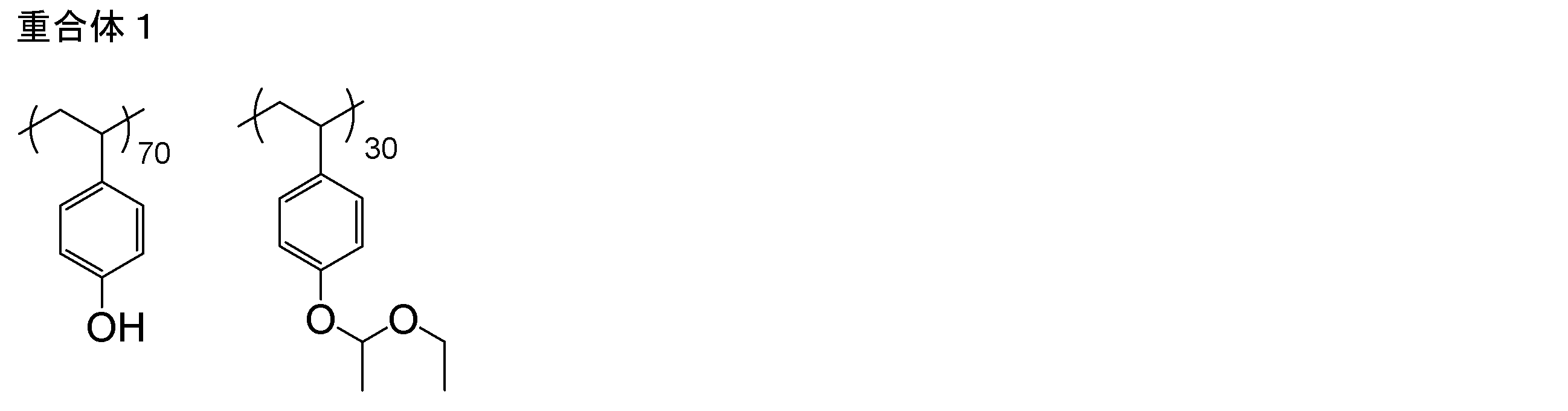
アルカリ可溶性樹脂(VP-8000 日本曹達(株)社製)15.6gおよびプロピレングリコールモノメチルエーテルアセテート(PGMEA)100gをフラスコ中で溶解し、減圧蒸留を行い、水とPGMEAを共沸留去した。含水が十分低くなったことを確認した後、2,3-ジヒドロフラン2.7gおよびp-トルエンスルホン酸0.015gを加え、室温にて2時間撹拌した。そこへトリエチルアミンを0.090g加えて反応を止めた。反応液に酢酸エチルを添加、さらに水洗した後、減圧留去によって酢酸エチル、水を留去し、保護率25モル%の可溶性樹脂である重合体2を得た。得られた樹脂の重量平均分子量は12,000であった。また、多分散度は、1.13であった。
重合体2の構造は、p-ヒドロキシスチレンの2-テトラヒドロフラニル保護体/p-ヒドロキシスチレン共重合体(30モル%/70モル%)である。

重合体3を以下のごとく合成した。
エチルビニルエーテル144.2部(2モル当量)にフェノチアジン0.5部を添加し、反応系中を10℃以下に冷却しながらメタクリル酸86.1部(1モル当量)を滴下後、室温(25℃)で4時間撹拌した。p-トルエンスルホン酸ピリジニウム5.0部を添加後、室温で2時間撹拌し、一夜室温放置した。反応液に炭酸水素ナトリウム5部および硫酸ナトリウム5部を添加し、室温で1時間撹拌し、不溶物を濾過後40℃以下で減圧濃縮し、残渣の黄色油状物を減圧蒸留して沸点(bp.)43~45℃/7mmHg留分のメタクリル酸1-エトキシエチル(MAEVE)134.0部を無色油状物として得た。
得られたメタクリル酸1-エトキシエチル(63.28部(0.4モル当量))、BzMA(52.83部(0.3モル当量))、MAA(8.61部(0.1モル当量))、HEMA(26.03部(0.2モル当量))およびEDM(110.8部)の混合溶液を窒素気流下、70℃に加熱した。この混合溶液を撹拌しながら、ラジカル重合開始剤V-65(商品名、和光純薬工業(株)製、4部)およびEDM(100.0部)の混合溶液を2.5時間かけて滴下した。滴下が終了してから、70℃で4時間反応させることにより、重合体のEDM溶液(固形分濃度:40%)を得た。
得られた重合体3のゲルパーミエーションクロマトグラフィー(GPC)により測定した重量平均分子量は、15,000であった。
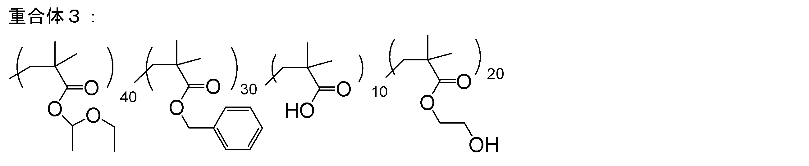
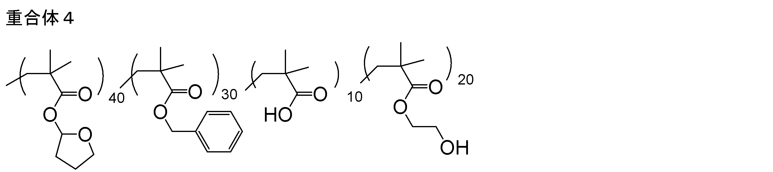
PAG-1:特表2002-528451号公報の段落0108に記載の方法に従って合成した。

C1:下記化合物(製造元:ダイセル化学工業株式会社製、品番:セロキサイド2021P)




C6:下記化合物(ナガセケムテックス株式会社製、品番:EX-321L)

PGMEA:メトキシプロピルアセテート(昭和電工社製)
PGDA:1,2-プロパンジオールジアセタート(沸点190℃、製造元:株式会社ダイセル社製 品番:PGDA)
1,3-BGDA:1,3-ブタンジオールジアセテート(沸点232℃、製造元:株式会社ダイセル社製 品番:1,3-BGDA)
1,6-HDDA:1,6-ヘキサンジオールジアセタート(沸点260℃、製造元:株式会社ダイセル社製 品番:1,6-HDDA)
DRA-150:トリアセチン(沸点260℃、製造元:株式会社ダイセル社製 品番:DRA-150)
DPNB:ジプロピレングリコール-n-ブチルエーテル(沸点229℃、製造元:株式会社ダイセル社製 品番:DPNB)
BDGAC:ジエチレングリコールモノブチルエーテルアセテート(沸点247℃、製造元:株式会社ダイセル社製 品番:DPNB)
G-1(製造元:川崎化成工業製、品番:9,10-ジブトキシアントラセン)

H-1:(製造元:東洋化成工業製、品番:CMTU)

下記表に示す組成となるように、各成分を溶解混合し、口径0.2μmのポリテトラフルオロエチレン製フィルターで濾過して、実施例および比較例の感光性樹脂組成物を得た。尚、配合比は下記表のとおりとした。
・(A)重合体 表に示す割合(重量比)で、(A1)と(A2)をブレンドした。
・(B)光酸発生剤 (A)重合体100重量部に対し、3.0重量%
・脂環式エポキシ化合物 (A)重合体100重量部に対し、下記表に記載の通りの量を配合した。
・(D1)溶剤 全溶剤に対して、下記表に記載の通りの量を配合した。
・(D2)溶剤 不揮発分が組成物に対して20重量%となるように調製した。
・塩基性化合物 (A)重合体100重量部に対し、0.2重量%
・増感剤 (A)重合体100重量部に対し、3.0重量%
洗浄、HMDS処理したガラス基板に1.3μmの膜厚で塗布し、マスクを介して露光現像し10μmのラインアンドスペースパターンがちょうど10μmとなる露光量を最適露光量として感度を評価した。3以上が実用レベルである。
1:100mJ/cm2以上の露光量を必要
2:50mJ/cm2以上100mJ/cm2未満の露光量が必要
3:20mJ/cm2以上50mJ/cm2未満の露光量が必要
4:10mJ/cm2以上20mJ未満の露光量
5:10mJ/cm2未満の露光量
洗浄、HMDS処理したガラス基板に1.3μmの膜厚で塗布し、マスクを介して10μmのラインアンドスペースパターンがちょうど10μmとなる露光量にて露光、現像し、かかるラインアンドスペースパターン付き基板を10枚準備し、基板1枚ごとに10点、光学式計測器ZYGO New View7200(ZYGO corp.製)にて、10μmのライン幅を測定し、計100点の実測線幅の標準偏差(σ)を計算した。評価基準は下記の通りであり、3以上が実用レベルである。
1:標準偏差σが0.4μm以上
2:標準偏差σが0.2μm以上、0.4μm未満
3:標準偏差σが0.15μm以上、0.25μm未満
4:標準偏差σが0.1μm以上、0.15μm未満
5:標準偏差σが0.1μm未満
洗浄、HMDS処理したガラス基板に1.3μmの膜厚で塗布し、マスクを介して露光現像し、ラインアンドスペースパターンのうち解像しうる最も小さなパターンを解像度とした。3以上が実用レベルである。
1:解像度が5μm以上
2:3.0μmが解像するが2.5μmは解像しない
3:2.5μmが解像するが2.0μmは解像しない
4:2.0μmが解像するが1.5μmは解像しない
5:1.5μmが解像する。
洗浄、HMDS処理したガラス基板に1.3μmの膜厚で塗布し、マスクを介して10μmのラインアンドスペースパターンがちょうど10μmとなる露光量にて露光、現像して形成した基板を、ホットプレートを用いて140℃の温度で3分間PostBakeし、3μmのL&Sの画素のテーパー角度を測定しこれを矩形性とした。3以上が実用レベルである。
1:テーパー角度が30°未満
2:テーパー角度が30°以上45°未満
3:テーパー角度が45°以上60°未満
4:テーパー角度が60°以上75°未満
5:テーパー角度が75°以上

<有機EL表示装置>
ITOパターンを具備する有機EL表示装置を以下の方法で作製した(図1参照)。
ガラス基板6上にボトムゲート型のTFT1を形成し、このTFT1を覆う状態でSi3N4から成る絶縁膜3を形成した。次に、この絶縁膜3に、ここでは図示を省略したコンタクトホールを形成した後、このコンタクトホールを介してTFT1に接続される配線2(高さ1.0μm)を絶縁膜3上に形成した。この配線2は、TFT1間または、後の工程で形成される有機EL素子とTFT1とを接続するためのものである。
感光性樹脂組成物を塗布する際の塗布性は良好で、露光、現像、焼成の後に得られた硬化膜には、しわやクラックの発生は認められなかった。さらに、配線2の平均段差は500nm、作製した平坦化膜4の膜厚は2,000nmであった。
<液晶表示装置>
ITOパターンを具備する液晶表示装置を以下の方法で作製した。
特許第3321003号公報の図1に記載のアクティブマトリクス型液晶表示装置において、画素電極4を実施例1の感光性樹脂組成物をマスクとして用い形成し、実施例17の液晶表示装置を得た。
すなわち、上記実施例16における有機EL表示装置の第一電極5の形成方法と同様の方法で、画素電極4を形成した。
2:配線
3:絶縁膜
4:平坦化膜
5:第一電極
6:ガラス基板
7:コンタクトホール
8:絶縁膜
10:液晶表示装置
12:バックライトユニット
14,15:ガラス基板
16:TFT
17:硬化膜
18:コンタクトホール
19:ITO透明電極
20:液晶
22:カラーフィルター
Claims (13)
- (A1)下記一般式(1)で表される構成単位(a1)を有する重合体を含む重合体成分、
(B)光酸発生剤、
(C)脂環式エポキシ化合物、および
(D1)分子内にアセテート構造を2つ以上含有する溶剤、
を含有する感光性樹脂組成物。

- 前記(C)脂環式エポキシ化合物が、下記一般式(I)で表される化合物である、請求項1に記載の感光性樹脂組成物。

- 前記一般式(I)で表される化合物中のnが1または2である、請求項2に記載の感光性樹脂組成物。
- さらに、(A2)酸分解性基で保護された保護カルボキシル基を有する構成単位(a4)を有する重合体成分を含む、請求項1~3のいずれか1項に記載の感光性樹脂組成物。
- 前記構成単位(a4)が、下記一般式(A2’)で表される構成単位である、請求項4に記載の感光性樹脂組成物。

- 前記(C)脂環式エポキシ化合物の含有量が、全固形分量に対して0.05~5質量%である、請求項1~5のいずれか1項に記載の感光性樹脂組成物。
- 前記(D1)分子内にアセテート構造を2つ以上含有する溶剤と、(D1)分子内にアセテート構造を2つ以上含有する溶剤と異なる他の溶剤(D2)とを含む、請求項1~6のいずれか1項に記載の感光性樹脂組成物。
- 前記(D1)分子内にアセテート構造を2つ以上含有する溶剤の沸点が、130℃以上300℃未満である、請求項1~7のいずれか1項に記載の感光性樹脂組成物。
- 前記(D1)分子内にアセテート構造を2つ以上含有する溶剤の含有量が、前記感光性樹脂組成物の1~10質量%である、請求項1~8のいずれか1項に記載の感光性樹脂組成物。
- (1)基板の少なくとも一方の面に、請求項1~9のいずれか1項に記載の感光性樹脂組成物を塗布する工程、
(2)乾燥により有機溶剤を揮発させ、感光性樹脂組成物層を形成する工程、
(3)前記感光性樹脂組成物層を露光する工程、
(4)露光された前記感光性樹脂組成物層を現像する工程、を含むパターンの製造方法。 - 形成されたパターンをエッチング用レジストとして用いてエッチングを行う工程、および前記パターンをプラズマ処理または薬品処理により除去する工程、を含む、請求項10に記載のパターンの製造方法。
- 請求項1~9のいずれか1項に記載の感光性樹脂組成物を硬化させてなる硬化膜。
- 請求項10または11に記載のパターンの製造方法を含む、有機EL表示装置または液晶表示装置の製造方法。
Priority Applications (3)
| Application Number | Priority Date | Filing Date | Title |
|---|---|---|---|
| CN201380050374.8A CN104662476B (zh) | 2012-09-28 | 2013-08-08 | 感光性树脂组合物、图案的制造方法、硬化膜、有机el显示装置及液晶显示装置的制造方法 |
| JP2014538263A JP6096202B2 (ja) | 2012-09-28 | 2013-08-08 | 感光性樹脂組成物、これを用いたパターンの製造方法 |
| KR1020157006313A KR101729599B1 (ko) | 2012-09-28 | 2013-08-08 | 감광성 수지 조성물, 이것을 사용한 패턴의 제조 방법 |
Applications Claiming Priority (2)
| Application Number | Priority Date | Filing Date | Title |
|---|---|---|---|
| JP2012217500 | 2012-09-28 | ||
| JP2012-217500 | 2012-09-28 |
Publications (1)
| Publication Number | Publication Date |
|---|---|
| WO2014050324A1 true WO2014050324A1 (ja) | 2014-04-03 |
Family
ID=50387738
Family Applications (1)
| Application Number | Title | Priority Date | Filing Date |
|---|---|---|---|
| PCT/JP2013/071473 Ceased WO2014050324A1 (ja) | 2012-09-28 | 2013-08-08 | 感光性樹脂組成物、これを用いたパターンの製造方法 |
Country Status (5)
| Country | Link |
|---|---|
| JP (1) | JP6096202B2 (ja) |
| KR (1) | KR101729599B1 (ja) |
| CN (1) | CN104662476B (ja) |
| TW (1) | TWI588605B (ja) |
| WO (1) | WO2014050324A1 (ja) |
Cited By (7)
| Publication number | Priority date | Publication date | Assignee | Title |
|---|---|---|---|---|
| WO2015064555A1 (ja) * | 2013-10-28 | 2015-05-07 | 富士フイルム株式会社 | 感光性樹脂組成物、パターンの製造方法、硬化膜、有機el表示装置の製造方法、および液晶表示装置の製造方法 |
| WO2015064556A1 (ja) * | 2013-10-28 | 2015-05-07 | 富士フイルム株式会社 | 感光性樹脂組成物、パターンの製造方法、硬化膜、有機el表示装置の製造方法、および液晶表示装置の製造方法 |
| JP2018021174A (ja) * | 2016-07-20 | 2018-02-08 | 東京応化工業株式会社 | マイクロレンズパターン製造用ポジ型感光性樹脂組成物及びその用途 |
| JP2020077642A (ja) * | 2020-01-20 | 2020-05-21 | 昭和電工株式会社 | 感光性樹脂組成物、有機el素子隔壁、及び有機el素子 |
| TWI696891B (zh) * | 2015-12-09 | 2020-06-21 | 日商住友化學股份有限公司 | 光阻組成物及光阻圖案之製造方法 |
| TWI698706B (zh) * | 2015-03-31 | 2020-07-11 | 日商住友化學股份有限公司 | 光阻組合物及光阻圖案之製造方法 |
| WO2025204201A1 (ja) * | 2024-03-29 | 2025-10-02 | 三井化学Ictマテリア株式会社 | 表面保護用組成物および表面保護膜 |
Families Citing this family (7)
| Publication number | Priority date | Publication date | Assignee | Title |
|---|---|---|---|---|
| TWI743132B (zh) * | 2016-07-20 | 2021-10-21 | 日商東京應化工業股份有限公司 | 微透鏡圖型製造用正型感光性樹脂組成物及其之用途 |
| JP2020076945A (ja) * | 2018-09-21 | 2020-05-21 | 旭化成株式会社 | 感光性樹脂組成物 |
| WO2021024650A1 (ja) * | 2019-08-02 | 2021-02-11 | 富士フイルム株式会社 | 感光性転写部材、樹脂パターンの製造方法、回路配線の製造方法、タッチパネルの製造方法 |
| CN113816929A (zh) * | 2021-09-29 | 2021-12-21 | 西安瑞联新材料股份有限公司 | 脂肪族环氧化合物及其制备的灌封胶 |
| CN114276239B (zh) * | 2021-12-29 | 2023-10-27 | 徐州博康信息化学品有限公司 | 一种含缩酮结构酸敏感光刻胶树脂单体的制备方法 |
| WO2023228661A1 (ja) * | 2022-05-24 | 2023-11-30 | 日産化学株式会社 | 薬液耐性保護膜 |
| CN118852065B (zh) * | 2024-06-24 | 2025-09-12 | 中山大学 | 一种多官能脂环族环氧单体及其制备方法和应用 |
Citations (5)
| Publication number | Priority date | Publication date | Assignee | Title |
|---|---|---|---|---|
| JP2008158281A (ja) * | 2006-12-25 | 2008-07-10 | Az Electronic Materials Kk | パターン形成方法およびそれに用いる感光性樹脂組成物 |
| JP2008304902A (ja) * | 2007-03-27 | 2008-12-18 | Fujifilm Corp | ポジ型感光性樹脂組成物及びそれを用いた硬化膜形成方法 |
| JP2010152068A (ja) * | 2008-12-25 | 2010-07-08 | Tokyo Ohka Kogyo Co Ltd | レジスト組成物、およびレジストパターン形成方法 |
| JP2012163937A (ja) * | 2011-01-19 | 2012-08-30 | Fujifilm Corp | 感光性樹脂組成物、パターン並びにその製造方法、有機el表示装置、液晶表示装置及び半導体素子 |
| JP2013083937A (ja) * | 2011-09-29 | 2013-05-09 | Fujifilm Corp | 感光性樹脂組成物、硬化膜並びにその製造方法 |
Family Cites Families (6)
| Publication number | Priority date | Publication date | Assignee | Title |
|---|---|---|---|---|
| JP4979963B2 (ja) * | 2006-03-10 | 2012-07-18 | 株式会社Adeka | 光学材料用硬化性組成物及び光導波路 |
| KR20090010044A (ko) * | 2006-05-16 | 2009-01-28 | 닛산 가가쿠 고교 가부시키 가이샤 | 포지티브형 감광성 수지 조성물 및 이로부터 얻어지는 다공질막 |
| JP2010139171A (ja) * | 2008-12-12 | 2010-06-24 | Hitachi Appliances Inc | 冷媒圧縮機及び冷凍サイクル装置 |
| JP5486521B2 (ja) * | 2010-03-15 | 2014-05-07 | 富士フイルム株式会社 | ポジ型感光性樹脂組成物、硬化膜の形成方法、硬化膜、有機el表示装置、及び、液晶表示装置 |
| CN102193316B (zh) * | 2010-03-15 | 2015-11-18 | 富士胶片株式会社 | 正型感光性树脂组合物、固化膜的形成方法、固化膜、有机el显示装置以及液晶显示装置 |
| JP5495991B2 (ja) * | 2010-07-12 | 2014-05-21 | 富士フイルム株式会社 | 着色感光性樹脂組成物、硬化膜及びその製造方法、カラーフィルタ、並びに、表示装置 |
-
2013
- 2013-08-08 WO PCT/JP2013/071473 patent/WO2014050324A1/ja not_active Ceased
- 2013-08-08 JP JP2014538263A patent/JP6096202B2/ja active Active
- 2013-08-08 KR KR1020157006313A patent/KR101729599B1/ko active Active
- 2013-08-08 CN CN201380050374.8A patent/CN104662476B/zh active Active
- 2013-09-26 TW TW102134831A patent/TWI588605B/zh active
Patent Citations (5)
| Publication number | Priority date | Publication date | Assignee | Title |
|---|---|---|---|---|
| JP2008158281A (ja) * | 2006-12-25 | 2008-07-10 | Az Electronic Materials Kk | パターン形成方法およびそれに用いる感光性樹脂組成物 |
| JP2008304902A (ja) * | 2007-03-27 | 2008-12-18 | Fujifilm Corp | ポジ型感光性樹脂組成物及びそれを用いた硬化膜形成方法 |
| JP2010152068A (ja) * | 2008-12-25 | 2010-07-08 | Tokyo Ohka Kogyo Co Ltd | レジスト組成物、およびレジストパターン形成方法 |
| JP2012163937A (ja) * | 2011-01-19 | 2012-08-30 | Fujifilm Corp | 感光性樹脂組成物、パターン並びにその製造方法、有機el表示装置、液晶表示装置及び半導体素子 |
| JP2013083937A (ja) * | 2011-09-29 | 2013-05-09 | Fujifilm Corp | 感光性樹脂組成物、硬化膜並びにその製造方法 |
Cited By (7)
| Publication number | Priority date | Publication date | Assignee | Title |
|---|---|---|---|---|
| WO2015064555A1 (ja) * | 2013-10-28 | 2015-05-07 | 富士フイルム株式会社 | 感光性樹脂組成物、パターンの製造方法、硬化膜、有機el表示装置の製造方法、および液晶表示装置の製造方法 |
| WO2015064556A1 (ja) * | 2013-10-28 | 2015-05-07 | 富士フイルム株式会社 | 感光性樹脂組成物、パターンの製造方法、硬化膜、有機el表示装置の製造方法、および液晶表示装置の製造方法 |
| TWI698706B (zh) * | 2015-03-31 | 2020-07-11 | 日商住友化學股份有限公司 | 光阻組合物及光阻圖案之製造方法 |
| TWI696891B (zh) * | 2015-12-09 | 2020-06-21 | 日商住友化學股份有限公司 | 光阻組成物及光阻圖案之製造方法 |
| JP2018021174A (ja) * | 2016-07-20 | 2018-02-08 | 東京応化工業株式会社 | マイクロレンズパターン製造用ポジ型感光性樹脂組成物及びその用途 |
| JP2020077642A (ja) * | 2020-01-20 | 2020-05-21 | 昭和電工株式会社 | 感光性樹脂組成物、有機el素子隔壁、及び有機el素子 |
| WO2025204201A1 (ja) * | 2024-03-29 | 2025-10-02 | 三井化学Ictマテリア株式会社 | 表面保護用組成物および表面保護膜 |
Also Published As
| Publication number | Publication date |
|---|---|
| JP6096202B2 (ja) | 2017-03-15 |
| KR101729599B1 (ko) | 2017-04-24 |
| KR20150043421A (ko) | 2015-04-22 |
| CN104662476A (zh) | 2015-05-27 |
| CN104662476B (zh) | 2019-04-23 |
| JPWO2014050324A1 (ja) | 2016-08-22 |
| TW201413379A (zh) | 2014-04-01 |
| TWI588605B (zh) | 2017-06-21 |
Similar Documents
| Publication | Publication Date | Title |
|---|---|---|
| JP6096202B2 (ja) | 感光性樹脂組成物、これを用いたパターンの製造方法 | |
| JP6279614B2 (ja) | 感光性樹脂組成物、硬化膜の製造方法、硬化膜、液晶表示装置および有機el表示装置 | |
| JP5849152B2 (ja) | 化学増幅型ポジ型感光性樹脂組成物、硬化膜の製造方法、硬化膜、有機el表示装置および液晶表示装置 | |
| JP5593405B2 (ja) | 感光性樹脂組成物、硬化膜の製造方法、硬化膜、有機el表示装置および液晶表示装置 | |
| JP5531034B2 (ja) | 感光性樹脂組成物、硬化膜の形成方法、硬化膜、有機el表示装置及び液晶表示装置 | |
| JP6240147B2 (ja) | 感光性樹脂組成物、これを用いた硬化膜の製造方法、硬化膜、液晶表示装置および有機el表示装置 | |
| JP6038951B2 (ja) | 感光性樹脂組成物、硬化膜の製造方法、硬化膜、有機el表示装置および液晶表示装置 | |
| JP6209617B2 (ja) | 感光性樹脂組成物、パターンの製造方法、硬化膜、有機el表示装置の製造方法、および液晶表示装置の製造方法 | |
| WO2015087830A1 (ja) | 感光性樹脂組成物、硬化膜の製造方法、硬化膜、液晶表示装置および有機el表示装置 | |
| JP5941543B2 (ja) | 感光性樹脂組成物、硬化膜の製造方法、硬化膜、有機el表示装置および液晶表示装置 | |
| JP5914663B2 (ja) | 感光性樹脂組成物、硬化膜の製造方法、硬化膜、有機el表示装置および液晶表示装置 | |
| JP6216801B2 (ja) | 感光性樹脂組成物、パターンの製造方法、硬化膜、有機el表示装置の製造方法、および液晶表示装置の製造方法 | |
| JP2014071308A (ja) | 感光性樹脂組成物、これを用いた硬化膜の製造方法、硬化膜、液晶表示装置および有機el表示装置 | |
| JP2016071243A (ja) | 樹脂パターンの形成方法、パターンの形成方法、硬化膜、液晶表示装置、有機el表示装置、及び、タッチパネル表示装置 | |
| WO2015033879A1 (ja) | 感光性樹脂組成物、硬化膜の製造方法、硬化膜、液晶表示装置および有機el表示装置 | |
| JP5933735B2 (ja) | 感光性樹脂組成物、硬化膜の製造方法、硬化膜、有機el表示装置および液晶表示装置 | |
| JP2014010200A (ja) | 感光性樹脂組成物、硬化膜の製造方法、硬化膜、有機el表示装置および液晶表示装置 | |
| JPWO2013191155A1 (ja) | 感光性樹脂組成物、硬化膜の製造方法、硬化膜、有機el表示装置および液晶表示装置 | |
| JP2014071300A (ja) | 感光性樹脂組成物、これを用いた硬化膜の製造方法、硬化膜、液晶表示装置および有機el表示装置 | |
| WO2014175316A1 (ja) | 感光性樹脂組成物、硬化物及びその製造方法、樹脂パターン製造方法、硬化膜、液晶表示装置、並びに、有機el表示装置 | |
| JP2014044278A (ja) | 感光性樹脂組成物、硬化膜の製造方法、硬化膜、有機el表示装置および液晶表示装置 |
Legal Events
| Date | Code | Title | Description |
|---|---|---|---|
| 121 | Ep: the epo has been informed by wipo that ep was designated in this application |
Ref document number: 13840719 Country of ref document: EP Kind code of ref document: A1 |
|
| ENP | Entry into the national phase |
Ref document number: 20157006313 Country of ref document: KR Kind code of ref document: A |
|
| ENP | Entry into the national phase |
Ref document number: 2014538263 Country of ref document: JP Kind code of ref document: A |
|
| NENP | Non-entry into the national phase |
Ref country code: DE |
|
| 122 | Ep: pct application non-entry in european phase |
Ref document number: 13840719 Country of ref document: EP Kind code of ref document: A1 |