WO2014049967A1 - 積層構造体、薄膜トランジスタアレイおよびそれらの製造方法 - Google Patents
積層構造体、薄膜トランジスタアレイおよびそれらの製造方法 Download PDFInfo
- Publication number
- WO2014049967A1 WO2014049967A1 PCT/JP2013/005125 JP2013005125W WO2014049967A1 WO 2014049967 A1 WO2014049967 A1 WO 2014049967A1 JP 2013005125 W JP2013005125 W JP 2013005125W WO 2014049967 A1 WO2014049967 A1 WO 2014049967A1
- Authority
- WO
- WIPO (PCT)
- Prior art keywords
- electrode
- gate
- insulating film
- source
- electrode layer
- Prior art date
- Legal status (The legal status is an assumption and is not a legal conclusion. Google has not performed a legal analysis and makes no representation as to the accuracy of the status listed.)
- Ceased
Links
Images





















Classifications
-
- H—ELECTRICITY
- H10—SEMICONDUCTOR DEVICES; ELECTRIC SOLID-STATE DEVICES NOT OTHERWISE PROVIDED FOR
- H10D—INORGANIC ELECTRIC SEMICONDUCTOR DEVICES
- H10D86/00—Integrated devices formed in or on insulating or conducting substrates, e.g. formed in silicon-on-insulator [SOI] substrates or on stainless steel or glass substrates
- H10D86/01—Manufacture or treatment
- H10D86/021—Manufacture or treatment of multiple TFTs
- H10D86/0241—Manufacture or treatment of multiple TFTs using liquid deposition, e.g. printing
-
- H—ELECTRICITY
- H10—SEMICONDUCTOR DEVICES; ELECTRIC SOLID-STATE DEVICES NOT OTHERWISE PROVIDED FOR
- H10D—INORGANIC ELECTRIC SEMICONDUCTOR DEVICES
- H10D30/00—Field-effect transistors [FET]
- H10D30/01—Manufacture or treatment
- H10D30/021—Manufacture or treatment of FETs having insulated gates [IGFET]
- H10D30/0411—Manufacture or treatment of FETs having insulated gates [IGFET] of FETs having floating gates
-
- H—ELECTRICITY
- H10—SEMICONDUCTOR DEVICES; ELECTRIC SOLID-STATE DEVICES NOT OTHERWISE PROVIDED FOR
- H10D—INORGANIC ELECTRIC SEMICONDUCTOR DEVICES
- H10D30/00—Field-effect transistors [FET]
- H10D30/60—Insulated-gate field-effect transistors [IGFET]
- H10D30/68—Floating-gate IGFETs
-
- H—ELECTRICITY
- H10—SEMICONDUCTOR DEVICES; ELECTRIC SOLID-STATE DEVICES NOT OTHERWISE PROVIDED FOR
- H10D—INORGANIC ELECTRIC SEMICONDUCTOR DEVICES
- H10D86/00—Integrated devices formed in or on insulating or conducting substrates, e.g. formed in silicon-on-insulator [SOI] substrates or on stainless steel or glass substrates
- H10D86/40—Integrated devices formed in or on insulating or conducting substrates, e.g. formed in silicon-on-insulator [SOI] substrates or on stainless steel or glass substrates characterised by multiple TFTs
- H10D86/421—Integrated devices formed in or on insulating or conducting substrates, e.g. formed in silicon-on-insulator [SOI] substrates or on stainless steel or glass substrates characterised by multiple TFTs having a particular composition, shape or crystalline structure of the active layer
- H10D86/423—Integrated devices formed in or on insulating or conducting substrates, e.g. formed in silicon-on-insulator [SOI] substrates or on stainless steel or glass substrates characterised by multiple TFTs having a particular composition, shape or crystalline structure of the active layer comprising semiconductor materials not belonging to the Group IV, e.g. InGaZnO
-
- H—ELECTRICITY
- H10—SEMICONDUCTOR DEVICES; ELECTRIC SOLID-STATE DEVICES NOT OTHERWISE PROVIDED FOR
- H10D—INORGANIC ELECTRIC SEMICONDUCTOR DEVICES
- H10D86/00—Integrated devices formed in or on insulating or conducting substrates, e.g. formed in silicon-on-insulator [SOI] substrates or on stainless steel or glass substrates
- H10D86/40—Integrated devices formed in or on insulating or conducting substrates, e.g. formed in silicon-on-insulator [SOI] substrates or on stainless steel or glass substrates characterised by multiple TFTs
- H10D86/441—Interconnections, e.g. scanning lines
-
- H—ELECTRICITY
- H10—SEMICONDUCTOR DEVICES; ELECTRIC SOLID-STATE DEVICES NOT OTHERWISE PROVIDED FOR
- H10D—INORGANIC ELECTRIC SEMICONDUCTOR DEVICES
- H10D86/00—Integrated devices formed in or on insulating or conducting substrates, e.g. formed in silicon-on-insulator [SOI] substrates or on stainless steel or glass substrates
- H10D86/40—Integrated devices formed in or on insulating or conducting substrates, e.g. formed in silicon-on-insulator [SOI] substrates or on stainless steel or glass substrates characterised by multiple TFTs
- H10D86/471—Integrated devices formed in or on insulating or conducting substrates, e.g. formed in silicon-on-insulator [SOI] substrates or on stainless steel or glass substrates characterised by multiple TFTs having different architectures, e.g. having both top-gate and bottom-gate TFTs
-
- H—ELECTRICITY
- H10—SEMICONDUCTOR DEVICES; ELECTRIC SOLID-STATE DEVICES NOT OTHERWISE PROVIDED FOR
- H10D—INORGANIC ELECTRIC SEMICONDUCTOR DEVICES
- H10D86/00—Integrated devices formed in or on insulating or conducting substrates, e.g. formed in silicon-on-insulator [SOI] substrates or on stainless steel or glass substrates
- H10D86/40—Integrated devices formed in or on insulating or conducting substrates, e.g. formed in silicon-on-insulator [SOI] substrates or on stainless steel or glass substrates characterised by multiple TFTs
- H10D86/481—Integrated devices formed in or on insulating or conducting substrates, e.g. formed in silicon-on-insulator [SOI] substrates or on stainless steel or glass substrates characterised by multiple TFTs integrated with passive devices, e.g. auxiliary capacitors
-
- H—ELECTRICITY
- H10—SEMICONDUCTOR DEVICES; ELECTRIC SOLID-STATE DEVICES NOT OTHERWISE PROVIDED FOR
- H10D—INORGANIC ELECTRIC SEMICONDUCTOR DEVICES
- H10D86/00—Integrated devices formed in or on insulating or conducting substrates, e.g. formed in silicon-on-insulator [SOI] substrates or on stainless steel or glass substrates
- H10D86/40—Integrated devices formed in or on insulating or conducting substrates, e.g. formed in silicon-on-insulator [SOI] substrates or on stainless steel or glass substrates characterised by multiple TFTs
- H10D86/60—Integrated devices formed in or on insulating or conducting substrates, e.g. formed in silicon-on-insulator [SOI] substrates or on stainless steel or glass substrates characterised by multiple TFTs wherein the TFTs are in active matrices
-
- H—ELECTRICITY
- H10—SEMICONDUCTOR DEVICES; ELECTRIC SOLID-STATE DEVICES NOT OTHERWISE PROVIDED FOR
- H10W—GENERIC PACKAGES, INTERCONNECTIONS, CONNECTORS OR OTHER CONSTRUCTIONAL DETAILS OF DEVICES COVERED BY CLASS H10
- H10W72/00—Interconnections or connectors in packages
- H10W72/01—Manufacture or treatment
- H10W72/012—Manufacture or treatment of bump connectors, dummy bumps or thermal bumps
Definitions
- the present invention relates to a laminated structure, in particular, a thin film transistor used for an image display device or the like.
- amorphous silicon (a-Si) and polysilicon (poly-Si) thin film transistors are manufactured on a glass substrate.
- a-Si amorphous silicon
- poly-Si polysilicon
- TFT Thin FilmTransistor
- the function of the source and drain varies depending on the polarity of the voltage to be written, so the name cannot be determined by operation. Therefore, for convenience, one is called a source and the other is called a drain, and the names are unified.
- the one connected to the wiring is called a source, and the one connected to the pixel electrode is called a drain.
- TFTs can be produced at a low temperature of 200 ° C. or lower, and expectations for flexible displays using plastic substrates are increasing. In addition to the feature of flexibility, it is also expected to be light, hard to break, and thin. Moreover, an inexpensive and large-area display is expected by forming TFTs by printing.
- the present invention has been made in view of the state of the related art, and eliminates instability of connection between the first electrode and the second electrode, and reliably connects the first electrode and the second electrode. It is an object to provide a thin film transistor array and a manufacturing method thereof.
- a first invention includes a first electrode layer on an insulating substrate, a first insulating film thereon, a second electrode layer on the first electrode layer, A laminated structure having a third electrode layer on the first insulating layer and having a portion connecting the first electrode layer and the second electrode layer, the portion being a first electrode
- a laminated structure of a layer, an opening of the first insulating film, a second electrode layer, an opening of the second insulating film, and a third electrode layer, and the third electrode layer is within the opening of the second insulating film.
- a laminated structure characterized in that the connection between the first electrode layer and the second electrode layer on the first insulating film is relayed or reinforced.
- the second invention has a first electrode layer including a gate wiring, a gate electrode connected to the gate wiring, a capacitor wiring, and a capacitor electrode connected to the capacitor wiring on an insulating substrate, A gate insulating film is formed on the first electrode layer, and a source wiring, a source electrode connected to the source wiring, a drain electrode, and a pixel connected to the drain electrode are formed on the gate insulating film.
- a second electrode layer including an electrode, a semiconductor between the source electrode and the drain electrode, a gate electrode overlapping the semiconductor through a gate insulating film, and a capacitor electrode through the gate insulating film
- a thin film transistor characterized in that the third electrode layer relays or reinforces the connection between the first electrode layer and the second electrode layer on the gate insulating film in the opening of the interlayer insulating film. It is an array.
- a third invention has a common electrode around the thin film transistor array, the common electrode is composed of a gate side common electrode and a source side common electrode, and a gate protection element is provided between each gate wiring and the gate side common electrode.
- a source protection element between each source wiring and the source side common electrode, and the common electrode is directly connected to the ground potential or connected to the ground potential through a resistor, common to the gate side
- the electrode is a second electrode layer
- the source-side common electrode is a first electrode layer
- the gate protection element and / or the source protection element are two diode-connected thin film transistors connected in parallel in the opposite direction, Either two diode-connected thin film transistors are connected in series in the opposite direction or one floating gate transistor, Gate protection element gate electrode and drain electrode short circuit, source protection element gate electrode and drain electrode short circuit, gate wiring and gate protection element connection, source protection element and source side common
- the gate connection electrode and the source connection electrode of the thin film transistor array are both in the first electrode layer, and the portion connecting the source connection electrode and the source wiring is the third electrode layer.
- the gate connection electrode and the source connection electrode of the thin film transistor array are both in the second electrode layer, and the third electrode layer is the first electrode in the portion connecting the gate wiring and the gate connection electrode.
- a sixth invention has a first electrode layer including a source wiring, a source electrode connected to the source wiring, a drain electrode, and a pixel electrode connected to the drain electrode on an insulating substrate, A gate insulating film having a semiconductor between the source electrode and the drain electrode and having an opening on the pixel electrode, a gate wiring on the gate insulating film, and a gate electrode connected to the gate wiring; A second electrode layer including a capacitor wiring and a capacitor electrode connected to the capacitor wiring, wherein the gate electrode overlaps the semiconductor via the gate insulating film, and the capacitor electrode passes through the gate insulating film; Overlying the pixel electrode, having an interlayer insulating film having an opening over the gate insulating film opening on the pixel electrode, and having a third electrode layer including an upper pixel electrode connected to the pixel electrode through the opening Thin film tiger A register array having a portion connecting the first electrode layer and the second electrode layer, the portion including the first electrode layer, the opening of the gate insulating film, the second electrode layer, and the inter
- a seventh invention has a common electrode around the thin film transistor array, the common electrode is composed of a gate side common electrode and a source side common electrode, and a gate protection element is provided between each gate wiring and the gate side common electrode.
- a source protection element between each source wiring and the source side common electrode, and the common electrode is directly connected to the ground potential or connected to the ground potential through a resistor, common to the gate side
- the electrode is the first electrode layer
- the source-side common electrode is the second electrode layer
- the gate protection element and / or the source protection element are two diode-connected thin film transistors connected in parallel in the opposite direction, Either two diode-connected thin film transistors are connected in series in the opposite direction or one floating gate transistor, Short circuit portion between the drain electrode and the gate electrode of the gate protection element, a short circuit portion between the drain electrode and the gate electrode of the source protection element, a connection portion between the gate protection element and the gate wiring, a common electrode on the source side, and source protection
- the gate connection electrode and the source connection electrode of the thin film transistor array are both in the first electrode layer, and the third electrode layer is the first electrode in the portion connecting the gate connection electrode and the gate wiring.
- the thin film transistor array according to the sixth or seventh invention wherein the connection between the layer and the second electrode layer is relayed or reinforced.
- the gate connection electrode and the source connection electrode of the thin film transistor array are both in the second electrode layer, and the third electrode layer is the first electrode in the portion connecting the source wiring and the source connection electrode.
- a step of forming a first electrode layer on an insulating substrate a step of forming a first insulating film that opens at least part of the first electrode layer, and at least the first insulating film opening.
- Forming a second electrode layer so as to overlap or be close to a part of the first electrode layer, and an opening including at least a part of the first electrode layer and a part of the second electrode layer in the first insulating film opening Forming a second insulating film having at least a part of the first electrode layer in the first insulating film opening and a part of the second electrode layer in the second insulating film opening at least in the second insulating film opening; Forming a third electrode layer so as to connect the two, a method for producing a laminated structure, wherein the step of forming the second electrode layer is printing Is the method.
- a gate wiring, a gate electrode connected to the gate wiring, a capacitor wiring, a capacitor electrode connected to the capacitor wiring, a gate electrode of a protection element, and a source side are formed on an insulating substrate.
- a gate connection electrode, a gate wiring, a gate electrode connected to the gate wiring, a capacitor wiring, a capacitor electrode connected to the capacitor wiring, a source connection electrode A step of forming a first electrode layer including a step of forming a gate insulating film having an opening on the source connection electrode, a source wiring on a substrate on which the gate insulating film is formed, and a source connected thereto
- a step of forming a first electrode layer including a step of forming a gate insulating film having an opening on the source connection electrode, a source wiring on a substrate on which the gate insulating film is formed, and a source connected thereto
- Forming a second electrode layer including an electrode, a drain electrode, and a pixel electrode connected to the drain electrode forming a semiconductor between the source electrode and the drain electrode; over the pixel electrode and over the gate insulating film opening Forming an interlayer insulating film having an opening in the upper surface, an upper pixel electrode connected to the pixel electrode through the interlayer insulating film
- a step of forming a first electrode layer including a gate wiring, a gate electrode connected to the gate wiring, a capacitor wiring, and a capacitor electrode connected to the capacitor wiring on an insulating substrate.
- a source wiring, a source electrode connected to the source wiring, a drain electrode, a pixel electrode connected to the drain electrode, and a source electrode / drain electrode of a protection element are formed on an insulating substrate.
- a step of forming a first electrode layer including a gate side common wiring, a step of forming a semiconductor between the source electrode and the drain electrode, and a protective element on the substrate on which the first electrode layer and the semiconductor are formed Forming a gate insulating film having an opening in the drain electrode and the gate side common electrode, a gate wiring on the substrate on which the gate insulating film is formed, a gate electrode connected to the gate wiring, and a capacitor
- a source connection electrode, a source wiring, a source electrode connected to the source wiring, a drain electrode, a pixel electrode connected to the drain electrode, a gate connection electrode Forming a first electrode layer including: a step of forming a gate insulating film having an opening on the gate connection electrode; a gate wiring on the substrate on which the gate insulating film is formed; and A step of forming a second electrode layer including a connected gate electrode, a capacitor wiring, and a capacitor electrode connected to the capacitor wiring; a step of forming a semiconductor between the source electrode and the drain electrode; And forming an interlayer insulating film having an opening over the gate insulating film opening, an upper pixel electrode connected to the pixel electrode through the interlayer insulating film opening on the pixel electrode, and a gate connection electrode Forming a third electrode layer including a connection reinforcing electrode on a layer structure arranged in the order of gate insulating film opening ⁇ gate wiring ⁇ interlayer insulating film opening,
- a step of forming a first electrode layer including a source wiring, a source electrode connected to the source wiring, a drain electrode, and a pixel electrode connected to the drain electrode on an insulating substrate A step of forming a semiconductor between the source electrode and the drain electrode, a step of forming a gate insulating film having an opening on the source wiring, a gate connection electrode on the substrate on which the gate insulating film is formed, Forming a second electrode layer including a gate wiring, a gate electrode connected to the gate wiring, a capacitor wiring, a capacitor electrode connected to the capacitor wiring, and a source connection electrode; Forming an interlayer insulating film having an opening on the gate insulating film opening; an upper pixel electrode connected to the pixel electrode through the interlayer insulating film opening on the pixel electrode; Forming a third electrode layer including a connection reinforcing electrode on a layer structure arranged in the order of film opening ⁇ source connection electrode ⁇ interlayer insulating film opening, wherein
- the seventeenth aspect of the invention is the method for manufacturing a laminated structure according to the tenth aspect, wherein the step of forming at least the second electrode layer is reverse offset printing.
- An eighteenth aspect of the invention is the method for manufacturing a laminated structure according to the tenth or seventeenth aspect, wherein the step of forming at least the third electrode layer is screen printing or gravure offset printing.
- a nineteenth aspect of the invention is a method of manufacturing a thin film transistor array according to any one of the eleventh to sixteenth aspects, wherein the step of forming at least the second electrode layer is reverse offset printing.
- the thin film transistor array according to any one of the eleventh to sixteenth aspects and the nineteenth aspect wherein the step of forming at least the third electrode layer is screen printing or gravure offset printing. Is the method.
- connection of the first electrode and the second electrode is relayed or reinforced by the third electrode, so that a laminated structure in a stable connection state can be obtained.
- a stable bottom-gate type thin film transistor can be obtained by relaying or reinforcing the connection between the first electrode and the second electrode by the third electrode.
- connection between the first electrode and the second electrode is relayed or reinforced by the third electrode, whereby a top-gate thin film transistor in a stable connection state can be obtained.
- a method for manufacturing a laminated structure in a stable connection state in which the connection between the first electrode and the second electrode is reinforced by the third electrode is obtained.
- a laminated structure in a stable connection state particularly a thin film transistor, can be obtained.
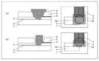
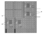
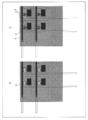
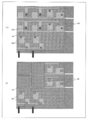
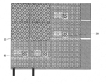
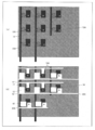
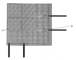
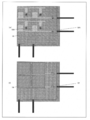
- FIG. 1 is a plan view and a cross-sectional view showing an example of the connection structure of the present invention.
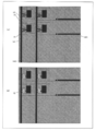
- FIG. 2 is a plan view and a cross-sectional view showing an example of the connection structure of the present invention.
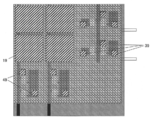
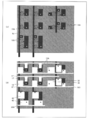
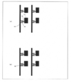
- FIG. 3 shows the present invention and is a plan view showing an example of a thin film transistor array with a protective element.
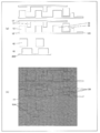
- FIG. 4 illustrates the present invention and is a circuit diagram illustrating an example of a protection element.
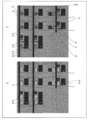
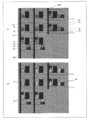
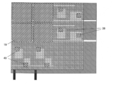
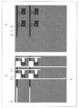
- FIG. 5 is a plan view showing an example of the thin film transistor array of the present invention.
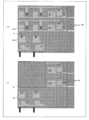
- FIG. 6 is a plan view showing a manufacturing process of the thin film transistor array of FIG.
- FIG. 7 is a plan view showing a manufacturing process of the thin film transistor array of FIG. FIG.
- FIG. 8 is a plan view showing a manufacturing process of the thin film transistor array of FIG.
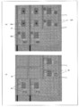
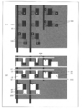
- FIG. 9 is a plan view showing an example of the thin film transistor array of the present invention.
- FIG. 10 is a plan view showing a manufacturing process of the thin film transistor array of FIG.
- FIG. 11 is a plan view showing a manufacturing process of the thin film transistor array of FIG.
- FIG. 12 is a plan view showing a manufacturing process of the thin film transistor array of FIG.
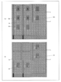
- FIG. 13 is a plan view showing an example of the thin film transistor array of the present invention.
- FIG. 14 is a plan view showing a manufacturing process of the thin film transistor array of FIG.
- FIG. 15 is a plan view showing a manufacturing process of the thin film transistor array of FIG. FIG.
- FIG. 16 is a plan view showing a manufacturing process of the thin film transistor array of FIG.
- FIG. 17 is a plan view showing an example of the thin film transistor array of the present invention.
- 18 is a plan view showing a manufacturing process of the thin film transistor array of FIG.
- FIG. 19 is a plan view showing a manufacturing process of the thin film transistor array of FIG.
- FIG. 20 is a plan view showing a manufacturing process of the thin film transistor array of FIG.
- FIG. 21 is a plan view showing an example of the thin film transistor array of the present invention.
- FIG. 22 is a plan view showing a manufacturing process of the thin film transistor array of FIG.
- FIG. 25 is a plan view showing an example of the thin film transistor array of the present invention.
- FIG. 26 is a plan view showing a manufacturing process of the thin film transistor array of FIG. 27 is a plan view showing a manufacturing process of the thin film transistor array of FIG.
- FIG. 28 is a plan view showing a manufacturing process of the thin film transistor array of FIG.
- FIG. 29 is a plan view showing an example of the thin film transistor array of the present invention.
- 30 is a plan view showing a manufacturing process of the thin film transistor array of FIG.
- FIG. 31 is a plan view showing a manufacturing process of the thin film transistor array of FIG.
- FIG. 32 is a plan view showing a manufacturing process of the thin film transistor array of FIG. FIG.
- FIG. 33 is a plan view showing an example of the thin film transistor array of the present invention.
- FIG. 34 is a plan view showing a manufacturing process of the thin film transistor array of FIG.
- FIG. 35 is a plan view showing a manufacturing process of the thin film transistor array of FIG.
- FIG. 36 is a plan view showing a manufacturing process of the thin film transistor array of FIG.
- FIG. 37 is a plan view showing an example of the thin film transistor array of the present invention.
- FIG. 38 is a plan view showing a manufacturing process of the thin film transistor array of FIG.
- FIG. 39 is a plan view showing a manufacturing process of the thin film transistor array of FIG.
- FIG. 40 is a plan view showing a manufacturing process of the thin film transistor array of FIG. FIG.
- FIG. 41 is a plan view showing an example of the thin film transistor array of the present invention.
- FIG. 42 is a plan view showing manufacturing steps of the thin film transistor array of FIG.
- FIG. 43 is a plan view showing a manufacturing process of the thin film transistor array of FIG.
- FIG. 44 is a plan view showing a manufacturing process of the thin film transistor array of FIG.
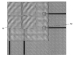
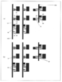
- FIG. 45 is a plan view showing an example of a conventional connection structure.
- FIGS. 1A shows a structure in which the connection of the conventional FIG. 45A is relayed.
- the third electrode 6 contacts the first electrode 2 in the opening of the first insulating film 3 and the first insulation.
- FIG. 1B shows a structure in which the connection in the conventional FIG. 45B is relayed, and the third electrode 6 contacts the second electrode 6 on the first electrode 2 in the opening of the first insulating film 3. At the same time, the first electrode 2 and the second electrode 4 are connected in contact with the second electrode 6 on the first insulating film 3.
- FIG. 1C shows a structure in which the connection shown in FIG. 45C is reinforced, and the second electrode 6 extends from the opening of the first insulating film 3 to the first insulating film 3. The connection between the first electrode 2 and the second electrode 4 is reinforced.
- the opening of the first insulating film 3 does not have to be completely above the first electrode 2, and the first electrode 2 only needs to be included in a part of the opening (FIGS. 2D and 2E).
- the second electrode 4 does not need to completely cover the opening of the first insulating film 3, and may be at least close to the opening of the first insulating film 3 (FIGS. 2D and 2E).
- the opening of the second insulating film 5 does not need to completely include the opening of the first insulating film 3 and is formed at least on the first electrode 2 and the first insulating film 3 in the opening of the first insulating film 3. It is only necessary to include the second electrode 4 close to the opening of the first insulating film 3 (FIG. 2E).
- the third electrode 6 need not completely include the opening of the second insulating film 5, and is formed on the first electrode 2 and the first insulating film 3 in at least the opening of the first insulating film 3. It is only necessary to include the second electrode 4 close to the opening of the insulating film 3 (FIG. 2E).
- the second electrode 4 completely includes the opening of the first insulating film 3 because it is an advantage of performing the second electrode 4 by a printing method. Since the printing method is an additive process, the influence on the lower layer is small and the first electrode 2 is not affected. In the case of photolithography + etching generally used for a silicon semiconductor, if the second electrode 4 does not completely cover the opening of the first insulating layer 3, the portion of the first electrode 2 that is not covered may be removed by etching.
- the laminated structure includes a first laminated structure having the first electrode layer on the insulating substrate, and a second laminated structure having the first insulating film on the first laminated structure.
- the laminated structure includes a portion connecting the first electrode layer and the second electrode layer, and the portion includes the first electrode layer, the opening of the first insulating film, the second electrode layer, A sixth laminated structure of the opening of the second insulating film and the third electrode layer, that is, the first electrode layer and the second electrode layer so as to pass through the region of the opening of the first insulating film and the opening of the second insulating film
- a sixth stacked structure is formed in which the third electrode layer is stacked, and in the opening of the second insulating film, the third electrode layer includes the first electrode layer and the second electrode layer on the first insulating film. Relay or reinforce the connection to.
- FIGS. These are bottom-gate type thin film transistors, and a portion connecting the first electrode 2 and the second electrode 4 is used as a protective element.
- the protective element protects the thin film transistor from electrostatic breakdown, and as shown in FIG. 3, between each wiring and the common electrode 20, that is, between the gate wiring 12 ′ and the gate common electrode 20G, or the source wiring 14 ′.
- the common electrode 20 is connected to the ground potential, the capacitor wiring 17 ′, or connected through a resistor.
- the gate side common electrode 20G and the source side common electrode 20S may be connected to each other, or each may be individually connected to the ground potential or the capacitor wiring 17 ′ via a resistor.
- a thin film transistor diode connection structure in which the drain 25 and the gate 22 are short-circuited is connected in parallel in the reverse direction (FIG. 4A), and the thin film transistor having the diode connection structure is reversed in the reverse direction.
- a serial connection (FIG. 4B), a floating gate type thin film transistor (FIG. 4C) in which the gate electrode 22 is not connected anywhere is used.
- FIG. 5 shows an example in which the protective element has a diode parallel structure.
- four pixel thin film transistors 10 including the upper pixel electrode 19
- two gate protection elements 30 including the connection reinforcing electrode 39
- two source protection elements 40 the connection reinforcing electrode 49. Is included).
- the manufacturing process is shown in FIGS.
- the substrate 1 may be an inorganic material such as glass, but an organic material such as plastic can also be used.
- an organic material such as plastic
- PET polyethylene terephthalate
- PEN polyethylene naphthalate
- PET polyethylene naphthalate
- PET polyethylene naphthalate
- PET polyether sulfone
- PI polyimide
- PEI polyetherimide
- PS polystyrene
- PVC polyvinyl chloride
- PE polyethylene
- PE polypropylene
- stacking and a mixture may be sufficient.
- the first electrode layer 2 including the electrode 42 and the source common electrode 20S is formed (FIG. 6A).
- a metal such as Al, Cr, Au, Ag, Ni, Cu, and Mo, or a transparent conductive film such as ITO can be used.
- a manufacturing method a method of forming by photolithography + etching after vapor deposition or sputtering film formation may be used, but a printing method (screen printing, flexographic printing, gravure printing, offset printing, reverse offset printing, etc.) can be used. When printing is used, Ag ink, Ni ink, Cu ink, or the like can be used.
- flexographic printing and reverse offset printing are suitable as the first electrode layer 2 because thin film printing is possible and flatness is excellent.
- a first insulating film 3 to be a gate insulating film 13 is formed on the substrate on which the first electrode layer 2 is formed.
- the gate insulating film 13 has an opening 13A (FIG. 6B).
- an organic insulating film such as polyvinylphenol, epoxy, or polyimide, or an inorganic insulating film such as SiO 2 , SiN, SiON, or Al 2 O 3 can be used.
- spin-coating, die-coating, etc. are used in the case of solvent-soluble organic substances, and in other cases, patterning is performed by photolithography, etching, lift-off, etc. after film formation using sputtering, vapor deposition, laser ablation, etc. Patterning can be performed directly by printing methods such as printing, reverse offset printing, ink jet printing, and exposure / development using a photosensitive organic material as a material.
- the second electrode layer 4 including the source electrode 34 of the element, the drain electrode 35 of the gate protection element, the source electrode 44 of the source protection element, and the drain electrode 45 of the source protection element is formed (FIG. 7C).
- a metal such as Au, Ag, Ni, or Cu, or a transparent conductive film such as ITO can be used.
- printing methods gravure printing, offset printing, reverse offset printing, etc.
- reverse offset printing has an excellent resolution and is optimal.
- a pixel thin film transistor semiconductor 16, a gate protection element semiconductor 36, and a source protection element semiconductor 46 are formed (FIG. 7D).
- the semiconductor 16 is formed so as to connect between the source electrode 14 and the drain electrode 15 of the pixel thin film transistor and to overlap the gate electrode 12 with the gate insulating film 13 interposed therebetween.
- the semiconductor 36 of the gate protection element is formed so as to connect between the source electrode 34 and the drain electrode 35 of the gate protection element and to overlap the gate electrode 32 of the gate protection element via the gate insulating film 13.
- the semiconductor 46 of the source protection element is formed so as to connect between the source electrode 44 and the drain electrode 45 of the source protection element and to overlap the gate electrode 42 of the source protection element with the gate insulating film 13 interposed therebetween.
- the present invention is a top contact structure in which the semiconductor is formed first and the second electrode layer 4 is formed thereon. But you can.
- a sealing layer (not shown) that covers at least the semiconductors 16, 36, and 46 may be provided.
- the semiconductors 16, 36, and 46 an organic semiconductor or an oxide semiconductor is used.
- organic semiconductors such as polythiophene derivatives, polyphenylene vinylene derivatives, polythienylene vinylene derivatives, polyallylamine derivatives, polyacetylene derivatives, acene derivatives, oligothiophene derivatives, InGaZnO series, ZnGaO series, InZnO series, InO series, GaO Oxide semiconductors such as Sn, SnO, or a mixture thereof can be used.
- Both organic semiconductors and oxide semiconductors can be formed by printing and baking a solution by flexographic printing, inkjet, or the like.
- a fluorinated resin is suitable.
- screen printing, gravure offset printing, ink jet and the like are suitable.
- the second insulating film 5 to be the interlayer insulating film 18 is formed on the substrate on which the second electrode layer 4 and the semiconductors 16, 36, 46 are formed.
- the interlayer insulating film 18 has an opening 18A (FIG. 8E).
- polyvinylphenol, acrylic, epoxy, polyimide, or the like is suitable.
- screen printing or gravure offset printing is suitable, but it may be formed by exposure / development after forming a photosensitive film.
- the third electrode layer 6 including the upper pixel electrode 19, the connection reinforcing electrode 39 of the gate protection element, and the connection reinforcing electrode 49 of the source protection element is formed ( FIG. 8 (f)).
- the upper pixel electrode 19 is connected to the pixel electrode 15 'through the interlayer insulating film opening 18A.
- the connection reinforcing electrode 39 of the gate protection element relays or reinforces the connection between the gate wiring 12 ′ and the drain electrode 35 of the gate protection element inside the interlayer insulating film opening 18A, and the gate electrode 32 and the gate protection element of the gate protection element.
- the connection of the drain electrode 35 is relayed or reinforced.
- connection reinforcement electrode 49 of the source protection element relays or reinforces the connection between the gate electrode 42 of the source protection element and the drain electrode 45 of the source protection element inside the interlayer insulating film opening 18A.
- a metal such as Al, Cr, Au, Ag, Ni, or Cu, a transparent conductive film such as ITO, or the like can be used.
- screen printing or gravure offset printing using Ag ink, Ni ink, Cu ink or the like. This is because screen printing and gravure offset printing are suitable for thick film printing.
- FIG. 9 shows an example in which the protective element has a diode series structure.
- four pixel thin film transistors 10 including the upper pixel electrode 19
- two gate protection elements 30 including the connection reinforcing electrode 39
- two source protection elements 40 the connection reinforcing electrode 49. Is included).
- the manufacturing process is shown in FIGS.
- the substrate 1 may be an inorganic material such as glass, but an organic material such as plastic can also be used.
- an organic material such as plastic
- PET polyethylene terephthalate
- PEN polyethylene naphthalate
- PET polyethylene naphthalate
- PET polyethylene naphthalate
- PET polyether sulfone
- PI polyimide
- PEI polyetherimide
- PS polystyrene
- PVC polyvinyl chloride
- PE polyethylene
- PE polypropylene
- stacking and a mixture may be sufficient.
- the first electrode layer 2 including the electrode 42 and the source common electrode 20S is formed (FIG. 10A).
- a metal such as Al, Cr, Au, Ag, Ni, Cu, and Mo, or a transparent conductive film such as ITO can be used.
- a manufacturing method a method of forming by photolithography + etching after vapor deposition or sputtering film formation may be used, but a printing method (screen printing, flexographic printing, gravure printing, offset printing, reverse offset printing, etc.) can be used. When printing is used, Ag ink, Ni ink, Cu ink, or the like can be used.
- flexographic printing and reverse offset printing are suitable as the first electrode layer 2 because thin film printing is possible and flatness is excellent.
- a first insulating film 3 to be a gate insulating film 13 is formed on the substrate on which the first electrode layer 2 is formed.
- the gate insulating film 13 has an opening 13A (FIG. 10B).
- an organic insulating film such as polyvinylphenol, epoxy, or polyimide, or an inorganic insulating film such as SiO 2 , SiN, SiON, or Al 2 O 3 can be used.
- spin-coating, die-coating, etc. are used in the case of solvent-soluble organic substances, and in other cases, patterning is performed by photolithography, etching, lift-off, etc. after film formation using sputtering, vapor deposition, laser ablation, etc. Patterning can be performed directly by printing methods such as printing, reverse offset printing, ink jet printing, and exposure / development using a photosensitive organic material as a material.
- the second electrode layer 4 including the source electrode 34 of the element, the drain electrode 35 of the gate protection element, the source electrode 44 of the source protection element, and the drain electrode 45 of the source protection element is formed (FIG. 11C).
- a metal such as Au, Ag, Ni, or Cu, or a transparent conductive film such as ITO can be used.
- printing methods gravure printing, offset printing, reverse offset printing, etc.
- reverse offset printing has an excellent resolution and is optimal.
- the pixel thin film transistor semiconductor 16, the gate protection element semiconductor 36, and the source protection element semiconductor 46 are formed (FIG. 11D).
- the semiconductor 16 is formed so as to connect between the source electrode 14 and the drain electrode 15 of the pixel thin film transistor and to overlap the gate electrode 12 with the gate insulating film 13 interposed therebetween.
- the semiconductor 36 of the gate protection element is formed so as to connect between the source electrode 34 and the drain electrode 35 of the gate protection element and to overlap the gate electrode 32 of the gate protection element via the gate insulating film 13.
- the semiconductor 46 of the source protection element is formed so as to connect between the source electrode 44 and the drain electrode 45 of the source protection element and to overlap the gate electrode 42 of the source protection element with the gate insulating film 13 interposed therebetween.
- the present invention is a top contact structure in which the semiconductor is formed first and the second electrode layer 4 is formed thereon. But you can.
- a sealing layer (not shown) that covers at least the semiconductors 16, 36, and 46 may be provided.
- the semiconductors 16, 36, and 46 an organic semiconductor or an oxide semiconductor is used.
- organic semiconductors such as polythiophene derivatives, polyphenylene vinylene derivatives, polythienylene vinylene derivatives, polyallylamine derivatives, polyacetylene derivatives, acene derivatives, oligothiophene derivatives, InGaZnO series, ZnGaO series, InZnO series, InO series, GaO Oxide semiconductors such as Sn, SnO, or a mixture thereof can be used.
- Both organic semiconductors and oxide semiconductors can be formed by printing and baking a solution by flexographic printing, inkjet, or the like.
- a fluorinated resin is suitable.
- screen printing, gravure offset printing, ink jet and the like are suitable.
- the second insulating film 5 to be the interlayer insulating film 18 is formed on the substrate on which the second electrode layer 4 and the semiconductors 16, 36, 46 are formed.
- the interlayer insulating film 18 has an opening 18A (FIG. 12E).
- polyvinylphenol, acrylic, epoxy, polyimide, or the like is suitable.
- screen printing or gravure offset printing is suitable, but it may be formed by exposure / development after forming a photosensitive film.
- the third electrode layer 6 including the upper pixel electrode 19, the connection reinforcing electrode 39 of the gate protection element, and the connection reinforcing electrode 49 of the source protection element is formed ( FIG. 12 (f)).
- the upper pixel electrode 19 is connected to the pixel electrode 15 'through the interlayer insulating film opening 18A.
- the connection reinforcing electrode 39 of the gate protection element relays or reinforces the connection between the gate electrode 12 of the gate protection element and the drain electrode 35 of the gate protection element inside the interlayer insulating film opening 18A.
- connection reinforcement electrode 49 of the source protection element relays or reinforces the connection between the gate electrode 42 of the source protection element and the drain electrode 45 of the source protection element inside the interlayer insulating film opening 18A.
- a metal such as Al, Cr, Au, Ag, Ni, or Cu, a transparent conductive film such as ITO, or the like can be used.
- screen printing or gravure offset printing using Ag ink, Ni ink, Cu ink or the like. This is because screen printing and gravure offset printing are suitable for thick film printing.
- FIG. 13 shows an example in which the protective element is a floating gate.
- the protective element is a floating gate.
- four pixel thin film transistors 10 including the upper pixel electrode 19
- two gate protection elements 30 including the connection reinforcing electrode 39
- two source protection elements 40 the connection reinforcing electrode 49. Is included).
- the manufacturing process is shown in FIGS.
- the substrate 1 may be an inorganic material such as glass, but an organic material such as plastic can also be used.
- an organic material such as plastic
- PET polyethylene terephthalate
- PEN polyethylene naphthalate
- PET polyethylene naphthalate
- PET polyethylene naphthalate
- PET polyether sulfone
- PI polyimide
- PEI polyetherimide
- PS polystyrene
- PVC polyvinyl chloride
- PE polyethylene
- PE polypropylene
- stacking and a mixture may be sufficient.
- the first electrode layer 2 including the electrode 42 and the source common electrode 20S is formed (FIG. 14A).
- a metal such as Al, Cr, Au, Ag, Ni, Cu, and Mo, or a transparent conductive film such as ITO can be used.
- a manufacturing method a method of forming by photolithography + etching after vapor deposition or sputtering film formation may be used, but a printing method (screen printing, flexographic printing, gravure printing, offset printing, reverse offset printing, etc.) can be used. When printing is used, Ag ink, Ni ink, Cu ink, or the like can be used.
- flexographic printing and reverse offset printing are suitable as the first electrode layer 2 because thin film printing is possible and flatness is excellent.
- a first insulating film 3 to be a gate insulating film 13 is formed on the substrate on which the first electrode layer 2 is formed.
- the gate insulating film 13 has an opening 13A (FIG. 14B).
- an organic insulating film such as polyvinylphenol, epoxy, or polyimide, or an inorganic insulating film such as SiO 2 , SiN, SiON, or Al 2 O 3 can be used.
- spin-coating, die-coating, etc. are used in the case of solvent-soluble organic substances, and in other cases, patterning is performed by photolithography, etching, lift-off, etc. after film formation using sputtering, vapor deposition, laser ablation, etc. Patterning can be performed directly by printing methods such as printing, reverse offset printing, ink jet printing, and exposure / development using a photosensitive organic material as a material.
- the second electrode layer 4 including the source electrode 34 of the element, the drain electrode 35 of the gate protection element, the source electrode 44 of the source protection element, and the drain electrode 45 of the source protection element is formed (FIG. 15C).
- a metal such as Au, Ag, Ni, or Cu, or a transparent conductive film such as ITO can be used.
- printing methods gravure printing, offset printing, reverse offset printing, etc.
- reverse offset printing has an excellent resolution and is optimal.
- a pixel thin film transistor semiconductor 16, a gate protection element semiconductor 36, and a source protection element semiconductor 46 are formed (FIG. 15D).
- the semiconductor 16 is formed so as to connect between the source electrode 14 and the drain electrode 15 of the pixel thin film transistor and to overlap the gate electrode 12 with the gate insulating film 13 interposed therebetween.
- the semiconductor 36 of the gate protection element is formed so as to connect between the source electrode 34 and the drain electrode 35 of the gate protection element and to overlap the gate electrode 32 of the gate protection element via the gate insulating film 13.
- the semiconductor 46 of the source protection element is formed so as to connect between the source electrode 44 and the drain electrode 45 of the source protection element and to overlap the gate electrode 42 of the source protection element with the gate insulating film 13 interposed therebetween.
- the present invention is a top contact structure in which the semiconductor is formed first and the second electrode layer 4 is formed thereon. But you can.
- a sealing layer (not shown) that covers at least the semiconductors 16, 36, and 46 may be provided.
- the semiconductors 16, 36, and 46 an organic semiconductor or an oxide semiconductor is used.
- organic semiconductors such as polythiophene derivatives, polyphenylene vinylene derivatives, polythienylene vinylene derivatives, polyallylamine derivatives, polyacetylene derivatives, acene derivatives, oligothiophene derivatives, InGaZnO series, ZnGaO series, InZnO series, InO series, GaO Oxide semiconductors such as Sn, SnO, or a mixture thereof can be used.
- Both organic semiconductors and oxide semiconductors can be formed by printing and baking a solution by flexographic printing, inkjet, or the like.
- a fluorinated resin is suitable.
- screen printing, gravure offset printing, ink jet and the like are suitable.
- the second insulating film 5 to be the interlayer insulating film 18 is formed on the substrate on which the second electrode layer 4 and the semiconductor layers 16, 36, 46 are formed.
- the interlayer insulating film 18 has an opening 18A (FIG. 16E).
- polyvinylphenol, acrylic, epoxy, polyimide, or the like is suitable.
- screen printing or gravure offset printing is suitable, but it may be formed by exposure / development after forming a photosensitive film.
- the third electrode layer 6 including the upper pixel electrode 19, the connection reinforcing electrode 39 of the gate protection element, and the connection reinforcing electrode 49 of the source protection element is formed ( FIG. 16 (f)).
- the upper pixel electrode 19 is connected to the pixel electrode 15 'through the interlayer insulating film opening 18A.
- the connection reinforcing electrode 39 of the gate protection element relays or reinforces the connection between the gate wiring 12 ′ and the drain electrode 35 of the gate protection element inside the interlayer insulating film opening 18 ⁇ / b> A.
- connection reinforcing electrode 49 of the source protection element relays or reinforces the connection between the source common electrode 20S and the drain electrode 45 of the source protection element inside the interlayer insulating film opening 18A.
- a metal such as Al, Cr, Au, Ag, Ni, or Cu, a transparent conductive film such as ITO, or the like can be used.
- screen printing or gravure offset printing using Ag ink, Ni ink, Cu ink or the like. This is because screen printing and gravure offset printing are suitable for thick film printing.
- FIGS. show bottom-gate thin film transistors, and the portion connecting the first electrode layer 2 and the second electrode layer 4 switches the wiring from the second electrode layer 4 to the first electrode layer 2, or the first electrode This is used for switching from the layer 2 to the second electrode layer 4.
- FIG. 17 shows the connection reinforcing electrode 54 of the source wiring for relaying or reinforcing the portion connecting the source wiring 14 ′ included in the second electrode layer 4 to the source connecting electrode 14 C included in the first electrode layer 2.
- four pixel thin film transistors 10 including the upper pixel electrode 19
- two gate wirings 12 ′ to 12C and two source wirings 14 ′ to 14C (connection reinforcement) Electrode 54.
- the manufacturing process is shown in FIGS.
- the substrate 1 may be an inorganic material such as glass, but an organic material such as plastic can also be used.
- an organic material such as plastic
- PET polyethylene terephthalate
- PEN polyethylene naphthalate
- PET polyethylene naphthalate
- PET polyethylene naphthalate
- PET polyether sulfone
- PI polyimide
- PEI polyetherimide
- PS polystyrene
- PVC polyvinyl chloride
- PE polyethylene
- PE polypropylene
- stacking and a mixture may be sufficient.
- the first electrode layer 2 including the gate electrode 12, the gate wiring 12 ′, the capacitor electrode 17, the capacitor wiring 17 ′, the gate connection electrode 12C, and the source connection electrode 14C is formed.
- a metal such as Al, Cr, Au, Ag, Ni, Cu, and Mo, or a transparent conductive film such as ITO can be used.
- a manufacturing method a method of forming by photolithography + etching after vapor deposition or sputtering film formation may be used, but a printing method (screen printing, flexographic printing, gravure printing, offset printing, reverse offset printing, etc.) can be used. When printing is used, Ag ink, Ni ink, Cu ink, or the like can be used.
- flexographic printing and reverse offset printing are suitable as the first electrode layer 2 because thin film printing is possible and flatness is excellent.
- a first insulating film 3 to be a gate insulating film 13 is formed on the substrate on which the first electrode layer 2 is formed.
- the gate insulating film 13 has an opening 13A (FIG. 18B).
- an organic insulating film such as polyvinylphenol, epoxy, or polyimide, or an inorganic insulating film such as SiO 2 , SiN, SiON, or Al 2 O 3 can be used.
- spin-coating, die-coating, etc. are used in the case of solvent-soluble organic substances, and in other cases, patterning is performed by photolithography, etching, lift-off, etc. after film formation using sputtering, vapor deposition, laser ablation, etc. Patterning can be performed directly by printing methods such as printing, reverse offset printing, ink jet printing, and exposure / development using a photosensitive organic material as a material.
- a second electrode layer 4 including a source electrode 14, a source wiring 14 ', a drain electrode 15, and a pixel electrode 15' is formed on the substrate on which the first insulating film 3 is formed (FIG. 19C). )).
- a metal such as Au, Ag, Ni, or Cu, or a transparent conductive film such as ITO can be used.
- printing methods gravure printing, offset printing, reverse offset printing, etc.
- reverse offset printing has an excellent resolution and is optimal.
- a pixel thin film transistor semiconductor 16 is formed (FIG. 19D).
- the semiconductor 16 is formed so as to connect between the source electrode 14 and the drain electrode 15 of the pixel thin film transistor and to overlap the gate electrode 12 with the gate insulating film 13 interposed therebetween.
- the structure shown above is a bottom contact structure in which a semiconductor is formed on the second electrode layer 4, the present invention is a top contact structure in which the semiconductor is formed first and the second electrode layer 4 is formed thereon. But you can.
- a sealing layer (not shown) that covers at least the semiconductor 16 may be provided.
- the semiconductor 16 an organic semiconductor or an oxide semiconductor is used.
- organic semiconductors such as polythiophene derivatives, polyphenylene vinylene derivatives, polythienylene vinylene derivatives, polyallylamine derivatives, polyacetylene derivatives, acene derivatives, oligothiophene derivatives, InGaZnO series, ZnGaO series, InZnO series, InO series, GaO Oxide semiconductors such as Sn, SnO, or a mixture thereof can be used.
- Both organic semiconductors and oxide semiconductors can be formed by printing and baking a solution by flexographic printing, inkjet, or the like.
- a fluorinated resin is suitable.
- screen printing, gravure offset printing, ink jet and the like are suitable.
- the second insulating film 5 to be the interlayer insulating film 18 is formed on the substrate on which the second electrode layer 4 and the semiconductor 16 are formed.
- the interlayer insulating film 18 has an opening 18A (FIG. 20E).
- polyvinylphenol, acrylic, epoxy, polyimide, or the like is suitable.
- screen printing or gravure offset printing is suitable, but it may be formed by exposure / development after forming a photosensitive film.
- the third electrode layer 6 including the upper pixel electrode 19 and the source line connection reinforcing electrode 54 is formed on the substrate on which the second insulating film 5 is formed (FIG. 20F).
- the upper pixel electrode 19 is connected to the pixel electrode 15 'through the interlayer insulating film opening 18A.
- the source line connection reinforcement electrode 54 relays or reinforces the connection between the source connection electrode 14C and the source line 14 'inside the interlayer insulating film opening 18A.
- a metal such as Al, Cr, Au, Ag, Ni, or Cu, a transparent conductive film such as ITO, or the like can be used.
- FIG. 21 shows the connection reinforcing electrode 52 of the gate wiring for relaying or reinforcing the portion connecting the gate wiring 12 ′ included in the first electrode layer 2 to the gate connection electrode 12 C included in the second electrode layer 4. It is an example.
- four thin film transistors 10 for pixels including the upper pixel electrode 19
- two gate wirings 12 ′ to 12C including the connection reinforcing electrode 52
- two source wirings 14 ′ To the source connection electrode 14C.
- the manufacturing process is shown in FIGS.
- the substrate 1 may be an inorganic material such as glass, but an organic material such as plastic can also be used.
- an organic material such as plastic
- PET polyethylene terephthalate
- PEN polyethylene naphthalate
- PET polyethylene naphthalate
- PET polyethylene naphthalate
- PET polyether sulfone
- PI polyimide
- PEI polyetherimide
- PS polystyrene
- PVC polyvinyl chloride
- PE polyethylene
- PE polypropylene
- stacking and a mixture may be sufficient.
- the first electrode layer 2 including the gate electrode 12, the gate wiring 12 ', the capacitor electrode 17, and the capacitor wiring 17' is formed on the substrate 1 (FIG. 22A).
- a metal such as Al, Cr, Au, Ag, Ni, Cu, and Mo, or a transparent conductive film such as ITO can be used.
- a manufacturing method a method of forming by photolithography + etching after vapor deposition or sputtering film formation may be used, but a printing method (screen printing, flexographic printing, gravure printing, offset printing, reverse offset printing, etc.) can be used. When printing is used, Ag ink, Ni ink, Cu ink, or the like can be used.
- flexographic printing and reverse offset printing are suitable as the first electrode layer 2 because thin film printing is possible and flatness is excellent.
- a first insulating film 3 to be a gate insulating film 13 is formed on the substrate on which the first electrode layer 2 is formed.
- the gate insulating film 13 has an opening 13A (FIG. 22B).
- an organic insulating film such as polyvinylphenol, epoxy, or polyimide, or an inorganic insulating film such as SiO 2 , SiN, SiON, or Al 2 O 3 can be used.
- spin-coating, die-coating, etc. are used in the case of solvent-soluble organic substances, and in other cases, patterning is performed by photolithography, etching, lift-off, etc. after film formation using sputtering, vapor deposition, laser ablation, etc. Patterning can be performed directly by printing methods such as printing, reverse offset printing, ink jet printing, and exposure / development using a photosensitive organic material as a material.
- a two-electrode layer 4 is formed (FIG. 23C).
- a metal such as Au, Ag, Ni, or Cu, or a transparent conductive film such as ITO can be used.
- printing methods gravure printing, offset printing, reverse offset printing, etc.
- reverse offset printing has an excellent resolution and is optimal.
- a pixel thin film transistor semiconductor 16 is formed (FIG. 23D).
- the semiconductor 16 is formed so as to connect between the source electrode 14 and the drain electrode 15 of the pixel thin film transistor and to overlap the gate electrode 12 with the gate insulating film 13 interposed therebetween.
- the structure shown above is a bottom contact structure in which a semiconductor is formed on the second electrode layer 4, the present invention is a top contact structure in which the semiconductor is formed first and the second electrode layer 4 is formed thereon. But you can.
- a sealing layer (not shown) that covers at least the semiconductor 16 may be provided.
- the semiconductor 16 an organic semiconductor or an oxide semiconductor is used.
- organic semiconductors such as polythiophene derivatives, polyphenylene vinylene derivatives, polythienylene vinylene derivatives, polyallylamine derivatives, polyacetylene derivatives, acene derivatives, oligothiophene derivatives, InGaZnO series, ZnGaO series, InZnO series, InO series, GaO Oxide semiconductors such as Sn, SnO, or a mixture thereof can be used.
- Both organic semiconductors and oxide semiconductors can be formed by printing and baking a solution by flexographic printing, inkjet, or the like.
- a fluorinated resin is suitable.
- screen printing, gravure offset printing, ink jet and the like are suitable.
- the second insulating film 5 to be the interlayer insulating film 18 is formed on the substrate on which the second electrode layer 4 and the semiconductor 16 are formed.
- the interlayer insulating film 18 has an opening 18A (FIG. 24E).
- polyvinylphenol, acrylic, epoxy, polyimide, or the like is suitable.
- screen printing or gravure offset printing is suitable, but it may be formed by exposure / development after forming a photosensitive film.
- the upper pixel electrode 19 and the connection reinforcing electrode 52 of the gate wiring are formed (FIG. 24F).
- the upper pixel electrode 19 is connected to the pixel electrode 15 'through the interlayer insulating film opening 18A.
- the connection reinforcing electrode 52 for the gate wiring relays or reinforces the connection between the gate wiring 12 'and the gate connecting electrode 12C inside the interlayer insulating film opening 18A.
- a metal such as Al, Cr, Au, Ag, Ni, or Cu, a transparent conductive film such as ITO, or the like can be used.
- the structure is a top gate type thin film transistor, and a portion connecting the first electrode 2 and the second electrode 4 is used as a protective element.
- the protective element protects the thin film transistor from electrostatic breakdown, and as shown in FIG. 3, between each wiring and the common electrode 20, that is, between the gate wiring 12 ′ and the gate common electrode 20G, or the source wiring 14 ′.
- the common electrode 20 is connected to the ground potential, the capacitor wiring 17 ′, or connected through a resistor.
- the gate side common electrode 20G and the source side common electrode 20S may be connected to each other, or each may be individually connected to the ground potential or the capacitor wiring 17 ′ via a resistor.
- a thin film transistor diode connection structure in which the drain 25 and the gate 22 are short-circuited is connected in parallel in the reverse direction (FIG. 4A), and the thin film transistor having the diode connection structure is reversed in the reverse direction.
- a serial connection (FIG. 4B), a floating gate type thin film transistor (FIG. 4C) in which the gate electrode 22 is not connected anywhere is used.
- FIG. 25 shows an example in which the protective element has a diode parallel structure.
- four pixel thin film transistors 10 including the upper pixel electrode 19
- two gate protection elements 30 including the connection reinforcing electrode 39
- two source protection elements 40 the connection reinforcing electrode 49. Is included).
- the manufacturing process is shown in FIGS.
- the substrate 1 may be an inorganic material such as glass, but an organic material such as plastic can also be used.
- an organic material such as plastic
- PET polyethylene terephthalate
- PEN polyethylene naphthalate
- PET polyethylene naphthalate
- PET polyethylene naphthalate
- PET polyether sulfone
- PI polyimide
- PEI polyetherimide
- PS polystyrene
- PVC polyvinyl chloride
- PE polyethylene
- PE polypropylene
- stacking and a mixture may be sufficient.
- the first electrode layer 2 including the drain electrode 35 of the gate protection element, the source electrode 44 of the source protection element, and the drain electrode 45 of the source protection element is formed (FIG. 26A).
- a metal such as Au, Ag, Ni, or Cu, or a transparent conductive film such as ITO can be used.
- printing methods gravure printing, offset printing, reverse offset printing, etc.
- reverse offset printing has an excellent resolution and is optimal.
- a pixel thin film transistor semiconductor 16, a gate protection element semiconductor 36, and a source protection element semiconductor 46 are formed (FIG. 26B).
- the semiconductor 16 is formed so as to connect the source electrode 14 and the drain electrode 15 of the pixel thin film transistor.
- the semiconductor 36 of the gate protection element is formed so as to connect between the source electrode 34 and the drain electrode 35 of the gate protection element.
- the semiconductor 46 of the source protection element is formed so as to connect between the source electrode 44 and the drain electrode 45 of the source protection element.
- organic semiconductors such as polythiophene derivatives, polyphenylene vinylene derivatives, polythienylene vinylene derivatives, polyallylamine derivatives, polyacetylene derivatives, acene derivatives, oligothiophene derivatives, InGaZnO series, ZnGaO series, InZnO series, InO series, GaO Oxide semiconductors such as Sn, SnO, or a mixture thereof can be used.
- Both organic semiconductors and oxide semiconductors can be formed by printing and baking a solution by flexographic printing, inkjet, or the like.
- a first insulating film 3 to be the gate insulating film 13 is formed on the substrate on which the first electrode layer 2 and the semiconductors 16, 36, and 46 are formed.
- the gate insulating film 13 has an opening 13A (FIG. 27C).
- an organic insulating film such as polyvinylphenol, epoxy, or polyimide, or an inorganic insulating film such as SiO 2 , SiN, SiON, or Al 2 O 3 can be used.
- spin-coating, die-coating, etc. are used in the case of solvent-soluble organic substances, and in other cases, patterning is performed by photolithography, etching, lift-off, etc. after film formation using sputtering, vapor deposition, laser ablation, etc. Patterning can be performed directly by printing methods such as printing, reverse offset printing, ink jet printing, and exposure / development using a photosensitive organic material as a material.
- the gate electrode 12 On the substrate on which the first insulating film 3 is formed, the gate electrode 12, the gate wiring 12 ′, the gate connection electrode 12C, the capacitor electrode 17, the capacitor wiring 17 ′, the gate electrode 32 of the gate protection element, Then, the second electrode layer 4 including the gate electrode 42 of the source protection element and the source common electrode 20S is formed (FIG. 27D).
- the gate electrode 12 is formed so as to overlap the semiconductor 16 of the pixel thin film transistor with the gate insulating film 13 interposed therebetween.
- the gate electrode 32 of the gate protection element is formed so as to overlap the semiconductor 36 of the gate protection element via the gate insulating film 13.
- the gate electrode 42 of the source protection element is formed so as to overlap the semiconductor 46 of the source protection element through the gate insulating film 13.
- a metal such as Al, Cr, Au, Ag, Ni, Cu, and Mo, or a transparent conductive film such as ITO can be used.
- a manufacturing method a method of forming by photolithography + etching after vapor deposition or sputtering film formation may be used, but a printing method (screen printing, flexographic printing, gravure printing, offset printing, reverse offset printing, etc.) can be used. When printing is used, Ag ink, Ni ink, Cu ink, or the like can be used.
- the second insulating film 5 to be the interlayer insulating film 18 is formed on the substrate on which the second electrode layer 4 is formed.
- the interlayer insulating film 18 has an opening 18A (FIG. 28E).
- polyvinylphenol, acrylic, epoxy, polyimide, or the like is suitable.
- screen printing or gravure offset printing is suitable, but it may be formed by exposure / development after forming a photosensitive film.
- the third electrode layer 6 including the upper pixel electrode 19, the connection reinforcing electrode 39 of the gate protection element, and the connection reinforcing electrode 49 of the source protection element is formed ( FIG. 28 (f)).
- the upper pixel electrode 19 is connected to the pixel electrode 15 'through the interlayer insulating film opening 18A.
- the connection reinforcing electrode 39 of the gate protection element relays or reinforces the connection between the gate wiring 12 ′ and the drain electrode 35 of the gate protection element inside the interlayer insulating film opening 18A, and the gate electrode 32 and the gate protection element of the gate protection element.
- the connection of the drain electrode 35 is relayed or reinforced.
- connection reinforcement electrode 49 of the source protection element relays or reinforces the connection between the gate electrode 42 of the source protection element and the drain electrode 45 of the source protection element inside the interlayer insulating film opening 18A.
- a metal such as Al, Cr, Au, Ag, Ni, or Cu, a transparent conductive film such as ITO, or the like can be used.
- screen printing or gravure offset printing using Ag ink, Ni ink, Cu ink or the like. This is because screen printing and gravure offset printing are suitable for thick film printing.
- FIG. 29 shows an example in which the protective element has a diode series structure.
- four pixel thin film transistors 10 including the upper pixel electrode 19
- two gate protection elements 30 including the connection reinforcing electrode 39
- two source protection elements 40 the connection reinforcing electrode 49. Is included).
- the manufacturing process is shown in FIGS.
- the substrate 1 may be an inorganic material such as glass, but an organic material such as plastic can also be used.
- an organic material such as plastic
- PET polyethylene terephthalate
- PEN polyethylene naphthalate
- PET polyethylene naphthalate
- PET polyethylene naphthalate
- PET polyether sulfone
- PI polyimide
- PEI polyetherimide
- PS polystyrene
- PVC polyvinyl chloride
- PE polyethylene
- PE polypropylene
- stacking and a mixture may be sufficient.
- the source electrode 14, the source wiring 14 ′, the source connection electrode 14 C, the drain electrode 15, the pixel electrode 15 ′, the gate common electrode 20 G, and the source electrode 34 of the gate protection element is formed (FIG. 30A).
- the first electrode layer 2 including the drain electrode 35 of the gate protection element, the source electrode 44 of the source protection element, and the drain electrode 45 of the source protection element is formed (FIG. 30A).
- a metal such as Au, Ag, Ni, or Cu, or a transparent conductive film such as ITO can be used.
- printing methods gravure printing, offset printing, reverse offset printing, etc.
- reverse offset printing has an excellent resolution and is optimal.
- a pixel thin film transistor semiconductor 16, a gate protection element semiconductor 36, and a source protection element semiconductor 46 are formed (FIG. 30B).
- the semiconductor 16 is formed so as to connect the source electrode 14 and the drain electrode 15 of the pixel thin film transistor.
- the semiconductor 36 of the gate protection element is formed so as to connect between the source electrode 34 and the drain electrode 35 of the gate protection element.
- the semiconductor 46 of the source protection element is formed so as to connect between the source electrode 44 and the drain electrode 45 of the source protection element.
- organic semiconductors such as polythiophene derivatives, polyphenylene vinylene derivatives, polythienylene vinylene derivatives, polyallylamine derivatives, polyacetylene derivatives, acene derivatives, oligothiophene derivatives, InGaZnO series, ZnGaO series, InZnO series, InO series, GaO Oxide semiconductors such as Sn, SnO, or a mixture thereof can be used.
- Both organic semiconductors and oxide semiconductors can be formed by printing and baking a solution by flexographic printing, inkjet, or the like.
- a first insulating film 3 to be the gate insulating film 13 is formed on the substrate on which the first electrode layer 2 and the semiconductors 16, 36, and 46 are formed.
- the gate insulating film 13 has an opening 13A (FIG. 31C).
- an organic insulating film such as polyvinylphenol, epoxy, or polyimide, or an inorganic insulating film such as SiO 2 , SiN, SiON, or Al 2 O 3 can be used.
- spin-coating, die-coating, etc. are used in the case of solvent-soluble organic substances, and in other cases, patterning is performed by photolithography, etching, lift-off, etc. after film formation using sputtering, vapor deposition, laser ablation, etc. Patterning can be performed directly by printing methods such as printing, reverse offset printing, ink jet printing, and exposure / development using a photosensitive organic material as a material.
- the gate electrode 12 On the substrate on which the first insulating film 3 is formed, the gate electrode 12, the gate wiring 12 ′, the gate connection electrode 12C, the capacitor electrode 17, the capacitor wiring 17 ′, the gate electrode 32 of the gate protection element, Then, the second electrode layer 4 including the gate electrode 42 of the source protection element and the source common electrode 20S is formed (FIG. 31D).
- the gate electrode 12 is formed so as to overlap the semiconductor 16 of the pixel thin film transistor with the gate insulating film 13 interposed therebetween.
- the gate electrode 32 of the gate protection element is formed so as to overlap the semiconductor 36 of the gate protection element via the gate insulating film 13.
- the gate electrode 42 of the source protection element is formed so as to overlap the semiconductor 46 of the source protection element through the gate insulating film 13.
- a metal such as Al, Cr, Au, Ag, Ni, Cu, and Mo, or a transparent conductive film such as ITO can be used.
- a manufacturing method a method of forming by photolithography + etching after vapor deposition or sputtering film formation may be used, but a printing method (screen printing, flexographic printing, gravure printing, offset printing, reverse offset printing, etc.) can be used. When printing is used, Ag ink, Ni ink, Cu ink, or the like can be used.
- the second insulating film 5 to be the interlayer insulating film 18 is formed on the substrate on which the second electrode layer 4 is formed.
- the interlayer insulating film 18 has an opening 18A (FIG. 32 (e)).
- polyvinylphenol, acrylic, epoxy, polyimide, or the like is suitable.
- screen printing or gravure offset printing is suitable, but it may be formed by exposure / development after forming a photosensitive film.
- the third electrode layer 6 including the upper pixel electrode 19, the connection reinforcing electrode 39 of the gate protection element, and the connection reinforcing electrode 49 of the source protection element is formed ( FIG. 32 (f)).
- the upper pixel electrode 19 is connected to the pixel electrode 15 'through the interlayer insulating film opening 18A.
- the connection reinforcing electrode 39 of the gate protection element relays or reinforces the connection between the gate electrode 32 of the gate protection element and the drain electrode 35 of the gate protection element inside the interlayer insulating film opening 18A.
- connection reinforcement electrode 49 of the source protection element relays or reinforces the connection between the gate electrode 42 of the source protection element and the drain electrode 45 of the source protection element inside the interlayer insulating film opening 18A.
- a metal such as Al, Cr, Au, Ag, Ni, or Cu, a transparent conductive film such as ITO, or the like can be used.
- screen printing or gravure offset printing using Ag ink, Ni ink, Cu ink or the like. This is because screen printing and gravure offset printing are suitable for thick film printing.
- FIG. 33 shows an example in which the protective element is a floating gate type thin film transistor.
- the protective element is a floating gate type thin film transistor.
- four pixel thin film transistors 10 including the upper pixel electrode 19
- two gate protection elements 30 including the connection reinforcing electrode 39
- two source protection elements 40 the connection reinforcing electrode 49. Is included).
- the manufacturing process is shown in FIGS.
- the substrate 1 may be an inorganic material such as glass, but an organic material such as plastic can also be used.
- an organic material such as plastic
- PET polyethylene terephthalate
- PEN polyethylene naphthalate
- PET polyethylene naphthalate
- PET polyethylene naphthalate
- PET polyether sulfone
- PI polyimide
- PEI polyetherimide
- PS polystyrene
- PVC polyvinyl chloride
- PE polyethylene
- PE polypropylene
- stacking and a mixture may be sufficient.
- the first electrode layer 2 including the drain electrode 35 of the gate protection element, the source electrode 44 of the source protection element, and the drain electrode 45 of the source protection element is formed (FIG. 34A).
- a metal such as Au, Ag, Ni, or Cu, or a transparent conductive film such as ITO can be used.
- printing methods gravure printing, offset printing, reverse offset printing, etc.
- reverse offset printing has an excellent resolution and is optimal.
- a pixel thin film transistor semiconductor 16, a gate protection element semiconductor 36, and a source protection element semiconductor 46 are formed (FIG. 34B).
- the semiconductor 16 is formed so as to connect the source electrode 14 and the drain electrode 15 of the pixel thin film transistor.
- the semiconductor 36 of the gate protection element is formed so as to connect between the source electrode 34 and the drain electrode 35 of the gate protection element.
- the semiconductor 46 of the source protection element is formed so as to connect between the source electrode 44 and the drain electrode 45 of the source protection element.
- organic semiconductors such as polythiophene derivatives, polyphenylene vinylene derivatives, polythienylene vinylene derivatives, polyallylamine derivatives, polyacetylene derivatives, acene derivatives, oligothiophene derivatives, InGaZnO series, ZnGaO series, InZnO series, InO series, GaO Oxide semiconductors such as Sn, SnO, or a mixture thereof can be used.
- Both organic semiconductors and oxide semiconductors can be formed by printing and baking a solution by flexographic printing, inkjet, or the like.
- a first insulating film 3 to be the gate insulating film 13 is formed on the substrate on which the first electrode layer 2 and the semiconductors 16, 36, and 46 are formed.
- the gate insulating film 13 has an opening 13A (FIG. 35C).
- an organic insulating film such as polyvinylphenol, epoxy, or polyimide, or an inorganic insulating film such as SiO 2 , SiN, SiON, or Al 2 O 3 can be used.
- spin-coating, die-coating, etc. are used in the case of solvent-soluble organic substances, and in other cases, patterning is performed by photolithography, etching, lift-off, etc. after film formation using sputtering, vapor deposition, laser ablation, etc. Patterning can be performed directly by printing methods such as printing, reverse offset printing, ink jet printing, and exposure / development using a photosensitive organic material as a material.
- the gate electrode 12 On the substrate on which the first insulating film 3 is formed, the gate electrode 12, the gate wiring 12 ′, the gate connection electrode 12C, the capacitor electrode 17, the capacitor wiring 17 ′, the gate electrode 32 of the gate protection element, Then, the second electrode layer 4 including the gate electrode 42 of the source protection element and the source common electrode 20S is formed (FIG. 35D).
- the gate electrode 12 is formed so as to overlap the semiconductor 16 of the pixel thin film transistor with the gate insulating film 13 interposed therebetween.
- the gate electrode 32 of the gate protection element is formed so as to overlap the semiconductor 36 of the gate protection element via the gate insulating film 13.
- the gate electrode 42 of the source protection element is formed so as to overlap the semiconductor 46 of the source protection element through the gate insulating film 13.
- a metal such as Al, Cr, Au, Ag, Ni, Cu, and Mo, or a transparent conductive film such as ITO can be used.
- a manufacturing method a method of forming by photolithography + etching after vapor deposition or sputtering film formation may be used, but a printing method (screen printing, flexographic printing, gravure printing, offset printing, reverse offset printing, etc.) can be used. When printing is used, Ag ink, Ni ink, Cu ink, or the like can be used.
- the second insulating film 5 to be the interlayer insulating film 18 is formed on the substrate on which the second electrode layer 4 is formed.
- the interlayer insulating film 18 has an opening 18A (FIG. 36E).
- polyvinylphenol, acrylic, epoxy, polyimide, or the like is suitable.
- screen printing or gravure offset printing is suitable, but it may be formed by exposure / development after forming a photosensitive film.
- the third electrode layer 6 including the upper pixel electrode 19, the connection reinforcing electrode 39 of the gate protection element, and the connection reinforcing electrode 49 of the source protection element is formed ( FIG. 36 (f)).
- the upper pixel electrode 19 is connected to the pixel electrode 15 'through the interlayer insulating film opening 18A.
- the connection reinforcing electrode 39 of the gate protection element relays or reinforces the connection between the gate wiring 12 ′ and the drain electrode 35 of the gate protection element inside the interlayer insulating film opening 18 ⁇ / b> A.
- connection reinforcing electrode 49 of the source protective element relays or reinforces the connection between the source wiring 14 ′ and the drain electrode 45 of the source protective element inside the interlayer insulating film opening 18 ⁇ / b> A.
- a metal such as Al, Cr, Au, Ag, Ni, or Cu, a transparent conductive film such as ITO, or the like can be used.
- screen printing or gravure offset printing using Ag ink, Ni ink, Cu ink or the like. This is because screen printing and gravure offset printing are suitable for thick film printing.
- FIGS. show top gate type thin film transistors, and the portion connecting the first electrode layer 2 and the second electrode layer 4 switches the wiring from the second electrode layer 4 to the first electrode layer 2, or the first electrode This is used for switching from the layer 2 to the second electrode layer 4.
- FIG. 37 shows the connection reinforcing electrode 52 of the gate wiring for relaying or reinforcing the portion connecting the gate wiring 12 ′ included in the second electrode layer 4 to the gate connecting electrode 12 C included in the first electrode layer 2.
- four thin film transistors 10 for pixels including the upper pixel electrode 19
- two gate wirings 12 ′ to 12C including the connection reinforcing electrode 52
- two source wirings 14 ′ To the source connection electrode 14C.
- the manufacturing process is shown in FIGS.
- the substrate 1 may be an inorganic material such as glass, but an organic material such as plastic can also be used.
- an organic material such as plastic
- PET polyethylene terephthalate
- PEN polyethylene naphthalate
- PET polyethylene naphthalate
- PET polyethylene naphthalate
- PET polyether sulfone
- PI polyimide
- PEI polyetherimide
- PS polystyrene
- PVC polyvinyl chloride
- PE polyethylene
- PE polypropylene
- stacking and a mixture may be sufficient.
- the first electrode layer 2 including the source electrode 14, the source wiring 14 ', the drain electrode 15, the pixel electrode 15', the gate connection electrode 12C, and the source connection electrode 14C is formed.
- a metal such as Al, Cr, Au, Ag, Ni, Cu, and Mo, or a transparent conductive film such as ITO can be used.
- printing methods gravure printing, offset printing, reverse offset printing, etc.
- reverse offset printing has an excellent resolution and is optimal.
- a pixel thin film transistor semiconductor 16 is formed (FIG. 38B).
- the semiconductor 16 is formed so as to connect the source electrode 14 and the drain electrode 15 of the pixel thin film transistor.
- the structure shown above is a bottom contact structure in which a semiconductor is formed on the second electrode layer 4, the present invention is a top contact structure in which the semiconductor is formed first and the second electrode layer 4 is formed thereon. But you can.
- the semiconductor 16 an organic semiconductor or an oxide semiconductor is used.
- organic semiconductors such as polythiophene derivatives, polyphenylene vinylene derivatives, polythienylene vinylene derivatives, polyallylamine derivatives, polyacetylene derivatives, acene derivatives, oligothiophene derivatives, InGaZnO series, ZnGaO series, InZnO series, InO series, GaO Oxide semiconductors such as Sn, SnO, or a mixture thereof can be used.
- Both organic semiconductors and oxide semiconductors can be formed by printing and baking a solution by flexographic printing, inkjet, or the like.
- a first insulating film 3 to be the gate insulating film 13 is formed on the substrate on which the first electrode layer 2 and the semiconductor 16 are formed.
- the gate insulating film 13 has an opening 13A (FIG. 39C).
- an organic insulating film such as polyvinylphenol, epoxy, or polyimide, or an inorganic insulating film such as SiO 2 , SiN, SiON, or Al 2 O 3 can be used.
- spin-coating, die-coating, etc. are used in the case of solvent-soluble organic substances, and in other cases, patterning is performed by photolithography, etching, lift-off, etc. after film formation using sputtering, vapor deposition, laser ablation, etc. Patterning can be performed directly by printing methods such as printing, reverse offset printing, ink jet printing, and exposure / development using a photosensitive organic material as a material.
- a second electrode layer 4 including a gate electrode 12, a gate wiring 12 ′, a capacitor electrode 17, and a capacitor wiring 17 ′ is formed on the substrate on which the first insulating film 3 is formed (FIG. 39D). )).
- the gate electrode 12 is formed so as to overlap the semiconductor 16 with the gate insulating film 13 interposed therebetween.
- a metal such as Au, Ag, Ni, or Cu, or a transparent conductive film such as ITO can be used.
- a manufacturing method a method of forming by photolithography + etching after vapor deposition or sputtering film formation may be used, but a printing method (screen printing, flexographic printing, gravure printing, offset printing, reverse offset printing, etc.) can be used. When printing is used, Ag ink, Ni ink, Cu ink, or the like can be used.
- the second insulating film 5 to be the interlayer insulating film 18 is formed on the substrate on which the second electrode layer 4 is formed.
- the interlayer insulating film 18 has an opening 18A (FIG. 40E).
- polyvinylphenol, acrylic, epoxy, polyimide, or the like is suitable.
- screen printing or gravure offset printing is suitable, but it may be formed by exposure / development after forming a photosensitive film.
- the third electrode layer 6 including the upper pixel electrode 19 and the connection reinforcing electrode 52 of the gate wiring is formed on the substrate on which the second insulating film 5 is formed (FIG. 40F).
- the upper pixel electrode 19 is connected to the pixel electrode 15 'through the interlayer insulating film opening 18A.
- the connection reinforcement electrode 52 of the gate wiring relays or reinforces the connection between the gate connection electrode 12C and the gate wiring 12 'inside the interlayer insulating film opening 18A.
- a metal such as Al, Cr, Au, Ag, Ni, or Cu, a transparent conductive film such as ITO, or the like can be used.
- FIG. 41 shows the case of the connection reinforcing electrode 54 of the source wiring for reinforcing the portion connecting the source wiring 14 ′ included in the first electrode layer 2 to the source connecting electrode 14 C included in the second electrode layer 4.
- the connection reinforcing electrode 54 of the source wiring for reinforcing the portion connecting the source wiring 14 ′ included in the first electrode layer 2 to the source connecting electrode 14 C included in the second electrode layer 4.
- four pixel thin film transistors 10 including the upper pixel electrode 19
- two gate wirings 12 ′ to 12C and two source wirings 14 ′ to 14C (connection reinforcement) Electrode 54.
- the manufacturing process is shown in FIGS.
- the substrate 1 may be an inorganic material such as glass, but an organic material such as plastic can also be used.
- an organic material such as plastic
- PET polyethylene terephthalate
- PEN polyethylene naphthalate
- PET polyethylene naphthalate
- PET polyethylene naphthalate
- PET polyether sulfone
- PI polyimide
- PEI polyetherimide
- PS polystyrene
- PVC polyvinyl chloride
- PE polyethylene
- PE polypropylene
- stacking and a mixture may be sufficient.
- the first electrode layer 2 including the source electrode 14, the source wiring 14 ', the drain electrode 15, and the pixel electrode 15' is formed on the substrate 1 (FIG. 42A).
- a metal such as Al, Cr, Au, Ag, Ni, Cu, and Mo, or a transparent conductive film such as ITO can be used.
- printing methods gravure printing, offset printing, reverse offset printing, etc.
- reverse offset printing has an excellent resolution and is optimal.
- a pixel thin film transistor semiconductor 16 is formed (FIG. 42B).
- the semiconductor 16 is formed so as to connect the source electrode 14 and the drain electrode 15 of the pixel thin film transistor.
- the structure shown above is a bottom contact structure in which a semiconductor is formed on the second electrode layer 4, the present invention is a top contact structure in which the semiconductor is formed first and the second electrode layer 4 is formed thereon. But you can.
- the semiconductor 16 an organic semiconductor or an oxide semiconductor is used.
- organic semiconductors such as polythiophene derivatives, polyphenylene vinylene derivatives, polythienylene vinylene derivatives, polyallylamine derivatives, polyacetylene derivatives, acene derivatives, oligothiophene derivatives, InGaZnO series, ZnGaO series, InZnO series, InO series, GaO Oxide semiconductors such as Sn, SnO, or a mixture thereof can be used.
- Both organic semiconductors and oxide semiconductors can be formed by printing and baking a solution by flexographic printing, inkjet, or the like.
- a first insulating film 3 to be the gate insulating film 13 is formed on the substrate on which the first electrode layer 2 and the semiconductor 16 are formed.
- the gate insulating film 13 has an opening 13A (FIG. 43C).
- an organic insulating film such as polyvinylphenol, epoxy, or polyimide, or an inorganic insulating film such as SiO 2 , SiN, SiON, or Al 2 O 3 can be used.
- spin-coating, die-coating, etc. are used in the case of solvent-soluble organic substances, and in other cases, patterning is performed by photolithography, etching, lift-off, etc. after film formation using sputtering, vapor deposition, laser ablation, etc. Patterning can be performed directly by printing methods such as printing, reverse offset printing, ink jet printing, and exposure / development using a photosensitive organic material as a material.
- the two-electrode layer 4 is formed (FIG. 43 (d)).
- the gate electrode 12 is formed so as to overlap the semiconductor 16 with the gate insulating film 13 interposed therebetween.
- a metal such as Au, Ag, Ni, or Cu, or a transparent conductive film such as ITO can be used.
- a method of forming by photolithography + etching after vapor deposition or sputtering film formation may be used, but a printing method (screen printing, flexographic printing, gravure printing, offset printing, reverse offset printing, etc.) can be used.
- a printing method screen printing, flexographic printing, gravure printing, offset printing, reverse offset printing, etc.
- Ag ink, Ni ink, Cu ink, or the like can be used.
- the second insulating film 5 to be the interlayer insulating film 18 is formed on the substrate on which the second electrode layer 4 is formed.
- the interlayer insulating film 18 has an opening 18A (FIG. 44E).
- polyvinylphenol, acrylic, epoxy, polyimide, or the like is suitable.
- screen printing or gravure offset printing is suitable, but it may be formed by exposure / development after forming a photosensitive film.
- the third electrode layer 6 including the upper pixel electrode 19 and the connection reinforcing electrode 54 of the source wiring is formed on the substrate on which the second insulating film 5 is formed (FIG. 44F).
- the upper pixel electrode 19 is connected to the pixel electrode 15 'through the interlayer insulating film opening 18A.
- the source line connection reinforcing electrode 54 relays or reinforces the connection between the source line 14 'and the source connection electrode 14C inside the interlayer insulating film opening 18A.
- a metal such as Al, Cr, Au, Ag, Ni, or Cu, a transparent conductive film such as ITO, or the like can be used.
- Example 1 An embodiment of the present invention will be described with reference to FIG. A structure in which FIGS. 1A to 1C coexist was produced.
- an Al film having a thickness of 50 nm was formed on the insulating substrate 1 by sputtering, and the first electrode layer 2 was formed by photolithography and etching.
- a photosensitive organic material was spin-coated, exposed and developed to form a first insulating film 3 having an opening 3A with a thickness of 1 ⁇ m.
- a pattern having a thickness of 50 nm was formed by performing reverse printing of Ag ink and baking at 180 ° C.
- the second insulating film 5 having the openings 5A was formed by screen printing / firing of epoxy resin, and the third electrode layer 6 was formed by screen printing / firing of Ag paste.
- Comparative Example 1 A comparative example will be described with reference to FIG. First, an Al film having a thickness of 50 nm was formed on the insulating substrate 1 by sputtering, and the first electrode layer 2 was formed by photolithography and etching. Next, a photosensitive organic material was spin-coated, exposed and developed to form a first insulating film 3 having an opening 3A with a thickness of 1 ⁇ m. Further, as the second electrode layer 4, a pattern having a thickness of 50 nm was formed by performing reverse printing of Ag ink and baking at 180 ° C.
- 45 (a) to 45 (c) are mixed in the structure thus manufactured.
- FIG. 45 (c) conduction between the first electrode layer 2 and the second electrode layer 4 was confirmed, but FIG. In the portions a) and (b), the first electrode layer 2 and the second electrode layer 4 were not conductive.
- Example 2 An embodiment of the present invention will be described with reference to FIG. 5 and FIGS.
- the device shown in FIG. 5 was fabricated by the steps of FIGS. 6 (a) to 8 (f).
- a photosensitive organic material was spin-coated, exposed and developed to form a gate insulating film 13 having an opening 13A, that is, a first insulating film 3 having an opening 3A having a thickness of 1 ⁇ m (FIG. 6B).
- the source electrode 14, the source wiring 14 ′, the drain electrode 15, the pixel electrode 15 ′, the source electrode 34 of the gate protection element, the drain electrode 35 of the gate protection element, and the source electrode 44 of the source protection element As a second electrode layer 4 including the drain electrode 45 of the source protection element, the gate side common electrode 20G, and the source connection electrode 14C, a pattern with a thickness of 50 nm is formed by reversal printing of Ag ink and baking at 180 ° C. It formed (FIG.7 (c)).
- the semiconductor layer 16, the semiconductor 36 of the gate protection element, and the semiconductor 46 of the source protection element were formed by ink-jet printing the polythiophene solution and baking at 100 ° C. (FIG. 7D).
- CYTOP which is a fluorinated resin, was screen-printed and fired to form a sealing layer that covers the semiconductors 16, 36, and 46 (not shown).
- the epoxy resin is screen printed and baked to form the interlayer insulating film 18 having the opening 18A, that is, the second insulating film 5 having the opening 5A (FIG. 8E), and the Ag paste is screen printed and baked.
- a third electrode layer 6 including the upper pixel electrode 19, a connection reinforcing electrode 39 of the gate protection element, and a connection reinforcing electrode 49 of the source protection element was formed (FIG. 8F).
- An electrophoretic display having a structure in which an electrophoretic display body is sandwiched between the thin film transistor array thus produced and a substrate with a counter electrode was produced. The display was confirmed with all pixels.
- Example 3 An embodiment of the present invention will be described with reference to FIGS. 9 and 10 to 12.
- the element shown in FIG. 9 was fabricated by the steps of FIGS. 10 (a) to 12 (f).
- a photosensitive organic material was spin-coated, exposed and developed to form a gate insulating film 13 having an opening 13A, that is, a first insulating film 3 having an opening 3A having a thickness of 1 ⁇ m (FIG. 10B).
- the source electrode 14, the source wiring 14 ′, the drain electrode 15, the pixel electrode 15 ′, the source electrode 34 of the gate protection element, the drain electrode 35 of the gate protection element, and the source electrode 44 of the source protection element As a second electrode layer 4 including the drain electrode 45 of the source protection element, the gate side common electrode 20G, and the source connection electrode 14C, a pattern with a thickness of 50 nm is formed by reversal printing of Ag ink and baking at 180 ° C. It formed (FIG.11 (c)).
- the semiconductor layer 16, the semiconductor 36 of the gate protection element, and the semiconductor 46 of the source protection element were formed by ink-jet printing the polythiophene solution and baking at 100 ° C. (FIG. 11D).
- CYTOP which is a fluorinated resin, was screen-printed and fired to form a sealing layer that covers the semiconductors 16, 36, and 46 (not shown).
- the epoxy resin is screen printed and baked to form the interlayer insulating film 18 having the opening 18A, that is, the second insulating film 5 having the opening 5A (FIG. 12E), and the Ag paste is screen printed and baked.
- a third electrode layer 6 including the upper pixel electrode 19, a connection reinforcing electrode 39 of the gate protection element, and a connection reinforcing electrode 49 of the source protection element was formed (FIG. 12F).
- An electrophoretic display having a structure in which an electrophoretic display body is sandwiched between the thin film transistor array thus produced and a substrate with a counter electrode was produced. The display was confirmed with all pixels.
- Example 4 An embodiment of the present invention will be described with reference to FIG. 13 and FIGS.
- the element shown in FIG. 13 was fabricated by the steps of FIGS. 14 (a) to 16 (f).
- a photosensitive organic material was spin-coated, exposed and developed to form a gate insulating film 13 having an opening 13A, that is, a first insulating film 3 having an opening 3A having a thickness of 1 ⁇ m (FIG. 14B).
- the source electrode 14, the source wiring 14 ′, the drain electrode 15, the pixel electrode 15 ′, the source electrode 34 of the gate protection element, the drain electrode 35 of the gate protection element, and the source electrode 44 of the source protection element As a second electrode layer 4 including the drain electrode 45 of the source protection element, the gate side common electrode 20G, and the source connection electrode 14C, a pattern with a thickness of 50 nm is formed by reversal printing of Ag ink and baking at 180 ° C. It formed (FIG.15 (c)).
- the polythiophene solution was flexographically printed and baked at 100 ° C. to form the semiconductor layer 16, the gate protection element semiconductor 36, and the source protection element semiconductor 46 (FIG. 15D).
- CYTOP which is a fluorinated resin
- CYTOP which is a fluorinated resin
- gravure offset printing / baking of epoxy resin is performed to form an interlayer insulating film 18 having an opening 18A, that is, a second insulating film 5 having an opening 5A (FIG. 16E), and gravure offset printing / baking is performed.
- the third electrode layer 6 including the upper pixel electrode 19, the connection reinforcing electrode 39 of the gate protective element, and the connection reinforcing electrode 49 of the source protective element was formed (FIG. 16F).
- An electrophoretic display having a structure in which an electrophoretic display body is sandwiched between the thin film transistor array thus produced and a substrate with a counter electrode was produced. The display was confirmed with all pixels.
- FIG. 17 was fabricated by the steps of FIGS. 18 (a) to 20 (f).
- a photosensitive organic material was spin-coated, exposed and developed to form a gate insulating film 13 having an opening 13A, that is, a first insulating film 3 having an opening 3A having a thickness of 1 ⁇ m (FIG. 18B).
- a second electrode layer 4 including the source electrode 14, the source wiring 14 ′, the drain electrode 15, and the pixel electrode 15 ′ a pattern having a thickness of 50 nm is obtained by performing reverse printing of Ag ink and baking at 180 ° C. Was formed (FIG. 19C).
- the semiconductor layer 16, the semiconductor 36 of the gate protection element, and the semiconductor 46 of the source protection element were formed by subjecting the polythiophene solution to inkjet printing and baking at 100 ° C. (FIG. 19D).
- CYTOP which is a fluorinated resin, was screen-printed and fired to form a sealing layer that covers the semiconductors 16, 36, and 46 (not shown).
- the epoxy resin is screen printed and baked to form the interlayer insulating film 18 having the opening 18A, that is, the second insulating film 5 having the opening 5A (FIG. 20E), and the Ag paste is screen printed and baked.
- a third electrode layer 6 including the upper pixel electrode 19 and the source line connection reinforcing electrode 54 was formed (FIG. 20F).
- An electrophoretic display having a structure in which an electrophoretic display body is sandwiched between the thin film transistor array thus produced and a substrate with a counter electrode was produced. The display was confirmed with all pixels.
- Example 6 An embodiment of the present invention will be described with reference to FIG. 21 and FIGS.
- the device shown in FIG. 21 was fabricated by the steps of FIGS. 22 (a) to 24 (f).
- a first ink including a gate electrode 12, a gate wiring 12 ′, a capacitor electrode 17 and a capacitor wiring 17 ′ is obtained by printing and baking Ag ink on the PEN which is the insulating substrate 1 by reverse offset printing.
- Electrode layer 2 was formed (FIG. 22A).
- a photosensitive organic material was spin-coated, exposed and developed to form a gate insulating film 13 having an opening 13A, that is, a first insulating film 3 having an opening 3A having a thickness of 1 ⁇ m (FIG. 22B). ).
- Ag ink is reversely printed as the second electrode layer 4 including the source electrode 14, the source wiring 14 ', the drain electrode 15, the pixel electrode 15', the gate connection electrode 12C, and the source connection electrode 14C.
- a pattern with a thickness of 50 nm was formed by baking at 180 ° C. (FIG. 23C).
- the polythiophene solution was flexographically printed and baked at 100 ° C. to form the semiconductor layer 16, the gate protection element semiconductor 36, and the source protection element semiconductor 46 (FIG. 23D).
- CYTOP which is a fluorinated resin, was screen-printed and fired to form a sealing layer that covers the semiconductors 16, 36, and 46 (not shown).
- gravure offset printing / baking of epoxy resin is performed to form the interlayer insulating film 18 having the opening 18A, that is, the second insulating film 5 having the opening 5A (FIG. 24E), and gravure offset printing / baking is performed.
- the third electrode layer 6 including the upper pixel electrode 19 and the connection reinforcing electrode 52 of the gate wiring was formed (FIG. 24F).
- An electrophoretic display having a structure in which an electrophoretic display body is sandwiched between the thin film transistor array thus produced and a substrate with a counter electrode was produced. The display was confirmed with all pixels.
- Example 7 An embodiment of the present invention will be described with reference to FIG. 25 and FIGS.
- the device shown in FIG. 25 was fabricated by the steps of FIGS. 26 (a) to 28 (f).
- Layer 2 was formed (FIG. 26 (a)).
- the semiconductor layer 16, the semiconductor 36 of the gate protection element, and the semiconductor 46 of the source protection element were formed by subjecting the polythiophene solution to inkjet printing and baking at 100 ° C. (FIG. 26B).
- a photosensitive organic material was spin-coated, exposed and developed to form a gate insulating film 13 having an opening 13A, that is, a first insulating film 3 having an opening 3A having a thickness of 1 ⁇ m (FIG. 27C). ).
- the epoxy resin is screen printed and baked to form the interlayer insulating film 18 having the opening 18A, that is, the second insulating film 5 having the opening 5A (FIG. 28E), and the Ag paste is screen printed and baked.
- An electrophoretic display having a structure in which an electrophoretic display body is sandwiched between the thin film transistor array thus produced and a substrate with a counter electrode was produced. The display was confirmed with all pixels.
- FIG. 29 An embodiment of the present invention will be described with reference to FIGS. 29 and 30 to 32.
- FIG. The element shown in FIG. 29 was fabricated by the steps of FIGS. 30 (a) to 32 (f).
- Layer 2 was formed (FIG. 30 (a)).
- the semiconductor layer 16, the semiconductor 36 of the gate protection element, and the semiconductor 46 of the source protection element were formed by ink-jet printing the polythiophene solution and baking at 100 ° C. (FIG. 30B).
- a photosensitive organic material was spin-coated, exposed and developed to form a gate insulating film 13 having an opening 13A, that is, a first insulating film 3 having an opening 3A having a thickness of 1 ⁇ m (FIG. 31C). ).
- the epoxy resin is screen printed and baked to form the interlayer insulating film 18 having the opening 18A, that is, the second insulating film 5 having the opening 5A (FIG. 32E), and the Ag paste is screen printed and baked.
- An electrophoretic display having a structure in which an electrophoretic display body is sandwiched between the thin film transistor array thus produced and a substrate with a counter electrode was produced. The display was confirmed with all pixels.
- Example 9 An embodiment of the present invention will be described with reference to FIG. 33 and FIGS.
- the device shown in FIG. 33 was fabricated by the steps of FIGS. 34 (a) to 36 (f).
- Layer 2 was formed (FIG. 34 (a)).
- the polythiophene solution was flexographically printed and baked at 100 ° C., thereby forming the semiconductor layer 16, the gate protection element semiconductor 36, and the source protection element semiconductor 46 (FIG. 34B).
- a photosensitive organic material was spin-coated, exposed and developed to form a gate insulating film 13 having an opening 13A, that is, a first insulating film 3 having an opening 3A having a thickness of 1 ⁇ m (FIG. 35C). ).
- An electrophoretic display having a structure in which an electrophoretic display body is sandwiched between the thin film transistor array thus produced and a substrate with a counter electrode was produced. The display was confirmed with all pixels.
- FIG. 37 was fabricated by the steps of FIGS. 38 (a) to 40 (f).
- a first electrode layer 2 including 12C and the source connection electrode 14C was formed (FIG. 38A).
- the semiconductor layer 16 was formed by subjecting the polythiophene solution to ink jet printing and baking at 100 ° C. (FIG. 38B).
- a photosensitive organic material was spin-coated, exposed and developed to form a gate insulating film 13 having an opening 13A, that is, a first insulating film 3 having an opening 3A having a thickness of 1 ⁇ m (FIG. 39C).
- a pattern having a thickness of 50 nm is obtained by performing reverse printing of Ag ink and baking at 180 ° C. (FIG. 39D).
- the epoxy resin is screen printed and baked to form the interlayer insulating film 18 having the opening 18A, that is, the second insulating film 5 having the opening 5A (FIG. 40E), and the Ag paste is screen printed and baked.
- An electrophoretic display having a structure in which an electrophoretic display body is sandwiched between the thin film transistor array thus produced and a substrate with a counter electrode was produced. The display was confirmed with all pixels.
- FIG. 41 An embodiment of the present invention will be described with reference to FIGS. 41 and 42 to 44.
- FIG. The device shown in FIG. 41 was fabricated by the steps of FIGS. 42 (a) to 44 (f).
- a first ink including a source electrode 14, a source wiring 14 ', a drain electrode 15, and a pixel electrode 15' is obtained by printing and baking Ag ink on the PEN that is the insulating substrate 1 by reverse offset printing.
- the electrode layer 2 was formed (FIG. 42 (a)).
- the semiconductor layer 16 was formed by flexographic printing of the polythiophene solution and baking at 100 ° C. (FIG. 42B).
- a photosensitive organic material is spin-coated, exposed and developed to form a gate insulating film 13 having an opening 13A, that is, a first insulating film 3 having an opening 3A, having a thickness of 1 ⁇ m (FIG. 43C).
- Ag ink is reversely printed as the second electrode layer 4 including the gate electrode 12, the gate wiring 12 ′, the capacitor electrode 17, the capacitor wiring 17 ′, the gate connection electrode 12C, and the source connection electrode 14C.
- a pattern having a thickness of 50 nm was formed by baking at 180 ° C. (FIG. 43D).
- An electrophoretic display having a structure in which an electrophoretic display body is sandwiched between the thin film transistor array thus produced and a substrate with a counter electrode was produced. The display was confirmed with all pixels.
- the present invention can be applied to displays such as liquid crystal displays and organic EL displays.
- Pixel Electrode 16 Semiconductor 17 Capacitor electrode 17 ′ Capacitor wiring 18 Interlayer insulating film 18A Interlayer insulating film opening 19 Upper pixel electrode 20 Common electrode 20G Gate common electrode 20S Source common electrode 30 Gate protection element 32 ... Gate electrode 34 of gate protection element ... Source power of gate protection element Electrode 35 ... Drain electrode 36 of gate protection element ... Semiconductor 39 of gate protection element ... Connection reinforcement electrode 40 of gate protection element ... Source protection element 42 ... Gate electrode 44 of source protection element ... Source electrode 45 of source protection element ... Source protection Element drain electrode 46 ... Source protection element semiconductor 49 ... Source protection element connection reinforcement electrode 52 ... Gate wiring connection reinforcement electrode 54 ... Source wiring connection reinforcement electrode
Landscapes
- Thin Film Transistor (AREA)
- Liquid Crystal (AREA)
- Electroluminescent Light Sources (AREA)
- Devices For Indicating Variable Information By Combining Individual Elements (AREA)
- Internal Circuitry In Semiconductor Integrated Circuit Devices (AREA)
- Semiconductor Integrated Circuits (AREA)
Abstract
積層構造体は、絶縁基板上に、第1電極層を有し、その上に第1絶縁膜を有し、その上に第2電極層を有し、その上に第2絶縁膜を有し、その上に第3電極層を有する構造体であって、第1電極層と第2電極層とを接続する部分を有し、その部分が、第1電極層と、第1絶縁膜の開口と、第2電極層と、第2絶縁膜の開口と、第3電極層との積層構造であり、第2絶縁膜の開口内において、第3電極層が、第1電極層と、第1絶縁膜上の第2電極層との接続を中継または補強する。
Description
本発明は、積層構造体、特には画像表示装置等に用いる薄膜トランジスタに関する。
半導体自体を基板としたトランジスタや集積回路技術を基礎として、ガラス基板上にアモルファスシリコン(a-Si)やポリシリコン(poly-Si)の薄膜トランジスタ(Thin Film Transistor:TFT)が製造され、液晶ディスプレイに応用されている(非特許文献1)。ここでTFTはスイッチの役割を果たしており、ゲート配線に与えられた選択電圧によってTFTをオンにした時に、ソース配線に与えられた信号電圧をドレインに接続された画素電極に書き込む。書き込まれた電圧は、画素電極/ゲート絶縁膜/キャパシタ電極によって構成される蓄積キャパシタに保持される。
ここで、TFTアレイの場合、ソースとドレインの働きは書き込む電圧の極性によって変わるため、動作で名称を決められない。そこで、便宜的に一方をソース、他方をドレインと、呼び方を統一しておく。本発明では、配線に接続されている方をソース、画素電極に接続されている方をドレインと呼ぶ。
近年、有機半導体や酸化物半導体が登場し、200℃以下の低温でTFTを作製できることが示され、プラスチック基板を用いたフレキシブルディスプレイへの期待が高まっている。フレキシブルという特長以外に、軽量、壊れにくい、薄型化できるというメリットも期待されている。また、印刷によってTFTを形成することにより、安価で大面積なディスプレイが期待されている。
松本正一編著:「液晶ディスプレイ技術 -アクティブマトリクスLCD-」産業図書,1996年11月
ところで、別の層の電極を接続することは、真空成膜とフォトリソ+エッチングを繰り返す工程では、容易であった。例えば基板上1に第1電極2を形成し、第1電極2上に開口を有する第1絶縁膜3を形成した試料に、第2電極4を形成する場合、第2電極4をスパッタや蒸着のような真空成膜法で形成すると絶縁層3の段差をカバーするのが容易だからである(なお、本明細書では、「フォトリソグラフィ」を適宜「フォトリソ」と簡略化して記載する)。その後、フォトリソおよびエッチングで第2電極4をパターニングすることで、図45(c)の構造を容易に得ることができる。
しかし、反転オフセット印刷、フレキソ印刷のような薄膜印刷法では、段差をカバーするのが難しい。例えば基板1上に第1電極2を形成し、第1電極2上に開口を有する第1絶縁層3を形成した試料に、第2電極4を印刷する際、図45(a)のように絶縁層3の上にだけ印刷される場合と、図45(b)のように絶縁層3の上と穴の底に印刷されるがそれらが分断されている場合と、図45(c)のように絶縁層3の上と穴の底が接続されている場合とが混在することが多い。図45(a)、図45(b)、図45(c)の左側の図は断面図、右側の図は平面図を示す。
このように、第1電極2と第2電極4との接続が不安定であるという問題があった。
本発明は、係る従来技術の状況に鑑みてなされたもので、第1電極と第2電極との接続不安定さを解消し、第1電極と第2電極とを確実に接続する積層構造体および薄膜トランジスタアレイ、ならびにそれらの製造方法を提供することを課題とする。
上記課題を解決するための、第1の発明は、絶縁基板上に第1電極層を有し、その上に第1絶縁膜を有し、その上に第2電極層を有し、その上に第2絶縁膜を有し、その上に第3電極層を有する積層構造体であって、第1電極層と第2電極層とを接続する部分を有し、その部分が、第1電極層と、第1絶縁膜の開口と、第2電極層と、第2絶縁膜の開口と、第3電極層との積層構造であり、第2絶縁膜の開口内において、第3電極層が、第1電極層と、第1絶縁膜上の第2電極層との接続を中継または補強することを特徴とする積層構造体である。
第2の発明は、絶縁基板上に、ゲート配線と、該ゲート配線に接続されたゲート電極と、キャパシタ配線と、該キャパシタ配線に接続されたキャパシタ電極とを含む第1電極層を有し、該第1電極層の上にゲート絶縁膜を有し、該ゲート絶縁膜の上に、ソース配線と、該ソース配線に接続されたソース電極と、ドレイン電極と、該ドレイン電極に接続された画素電極とを含む第2電極層を有し、ソース電極・ドレイン電極間に半導体を有し、ゲート電極がゲート絶縁膜を介して該半導体に重なっており、キャパシタ電極がゲート絶縁膜を介して該画素電極に重なっており、該画素電極上に開口を有する層間絶縁膜を有し、該開口を介して画素電極に接続された上部画素電極を含む第3電極層を有する薄膜トランジスタアレイであって、第1電極層と第2電極層とを接続する部分を有し、その部分が、第1電極層と、ゲート絶縁膜の開口と、第2電極層と、層間絶縁膜の開口と、第3電極層との積層構造であり、層間絶縁膜の開口内において、第3電極層が、第1電極層と、ゲート絶縁膜上の第2電極層との接続を中継または補強することを特徴とする薄膜トランジスタアレイである。
第3の発明は、前記薄膜トランジスタアレイの周囲に共通電極を有し、共通電極はゲート側共通電極とソース側共通電極とからなり、各ゲート配線とゲート側共通電極との間にゲート保護素子を有し、各ソース配線とソース側共通電極との間にソース保護素子を有し、共通電極はアース電位に直接接続されているか、あるいは抵抗を介してアース電位に接続されており、ゲート側共通電極は第2電極層であり、ソース側共通電極は第1電極層であり、該ゲート保護素子および/またはソース保護素子は薄膜トランジスタをダイオード接続したものを逆向きに2個並列接続したものか、薄膜トランジスタをダイオード接続したものを逆向きに2個直列接続したものか、あるいは1個のフローティングゲートトランジスタのいずれかであり、該ゲート保護素子のゲート電極とドレイン電極との短絡部と、ソース保護素子のゲート電極とドレイン電極との短絡部と、ゲート配線とゲート保護素子との接続部と、ソース保護素子とソース側共通電極との接続部との少なくとも1つが、第3電極層が第1電極層と第2電極層との接続を中継または補強する構造であることを特徴とする第2の発明に記載の薄膜トランジスタアレイである。
第4の発明は、前記薄膜トランジスタアレイのゲート接続電極およびソース接続電極がいずれも第1電極層にあり、該ソース接続電極と前記ソース配線とを接続する部分が、第3電極層が第1電極層と第2電極層との接続を中継または補強する構造であることを特徴とする第2または第3の発明に記載の薄膜トランジスタアレイである。
第5の発明は、前記薄膜トランジスタアレイのゲート接続電極およびソース接続電極がいずれも第2電極層にあり、前記ゲート配線と該ゲート接続電極とを接続する部分が、第3電極層が第1電極層と第2電極層との接続を中継または補強する構造であることを特徴とする第2または第3の発明に記載の薄膜トランジスタアレイである。
第6の発明は、絶縁基板上に、ソース配線と、該ソース配線に接続されたソース電極と、ドレイン電極と、該ドレイン電極に接続された画素電極とを含む第1電極層を有し、ソース電極・ドレイン電極間に半導体を有し、該画素電極上に開口を有するゲート絶縁膜を有し、該ゲート絶縁膜の上に、ゲート配線と、該ゲート配線に接続されたゲート電極と、キャパシタ配線と、該キャパシタ配線に接続されたキャパシタ電極とを含む第2電極層を有し、該ゲート電極がゲート絶縁膜を介して半導体に重なっており、該キャパシタ電極がゲート絶縁膜を介して画素電極に重なっており、該画素電極上のゲート絶縁膜開口上に開口を有する層間絶縁膜を有し、該開口を介して画素電極に接続された上部画素電極を含む第3電極層を有する薄膜トランジスタアレイであって、第1電極層と第2電極層とを接続する部分を有し、その部分が、第1電極層と、ゲート絶縁膜の開口と、第2電極層と、層間絶縁膜の開口と、第3電極層との積層構造であり、層間絶縁膜の開口内において、第3電極層が、第1電極層と、ゲート絶縁膜上の第2電極層との接続を中継または補強することを特徴とする薄膜トランジスタアレイである。
第7の発明は、前記薄膜トランジスタアレイの周囲に共通電極を有し、共通電極はゲート側共通電極とソース側共通電極とからなり、各ゲート配線とゲート側共通電極との間にゲート保護素子を有し、各ソース配線とソース側共通電極との間にソース保護素子を有し、共通電極はアース電位に直接接続されているか、あるいは抵抗を介してアース電位に接続されており、ゲート側共通電極は第1電極層であり、ソース側共通電極は第2電極層であり、該ゲート保護素子および/またはソース保護素子は薄膜トランジスタをダイオード接続したものを逆向きに2個並列接続したものか、薄膜トランジスタをダイオード接続したものを逆向きに2個直列接続したものか、あるいは1個のフローティングゲートトランジスタのいずれかであり、該ゲート保護素子のドレイン電極とゲート電極との短絡部と、ソース保護素子のドレイン電極とゲート電極との短絡部と、ゲート保護素子とゲート配線との接続部と、ソース側共通電極とソース保護素子との接続部との少なくとも1つが、第3電極層が第1電極層と第2電極層との接続を中継または補強する構造であることを特徴とする第6の発明に記載の薄膜トランジスタアレイである。
第8の発明は、前記薄膜トランジスタアレイのゲート接続電極およびソース接続電極がいずれも第1電極層にあり、該ゲート接続電極と前記ゲート配線とを接続する部分が、第3電極層が第1電極層と第2電極層との接続を中継または補強する構造であることを特徴とする第6または第7の発明に記載の薄膜トランジスタアレイである。
第9の発明は、前記薄膜トランジスタアレイのゲート接続電極およびソース接続電極がいずれも第2電極層にあり、前記ソース配線と該ソース接続電極とを接続する部分が、第3電極層が第1電極層と第2電極層との接続を中継または補強する構造であることを特徴とする第6または第7の発明に記載の薄膜トランジスタアレイである。
第10の発明は、絶縁基板上に、第1電極層を形成する工程と、少なくとも第1電極層の一部を開口する第1絶縁膜を形成する工程と、少なくとも該第1絶縁膜開口部の一部に重なるか近接するように第2電極層を形成する工程と、少なくとも該第1絶縁膜開口部内の第1電極層の一部と第2電極層の一部とを含むような開口を有する第2絶縁膜を形成する工程と、少なくとも第2絶縁膜開口内で第1絶縁膜開口内の第1電極層の一部と第2絶縁膜開口内の第2電極層の一部とを接続するように第3電極層を形成する工程と、を有する積層構造体の製造方法であって、該第2電極層を形成する工程が印刷であることを特徴とする積層構造体の製造方法である。
第11の発明は、絶縁基板上に、ゲート配線と、該ゲート配線に接続されたゲート電極と、キャパシタ配線と、該キャパシタ配線に接続されたキャパシタ電極と、保護素子のゲート電極と、ソース側共通配線とを含む第1電極層を形成する工程と、該第1電極層が形成された基板の上に保護素子のゲート電極とソース側共通電極とに開口を有するゲート絶縁膜を形成する工程と、該ゲート絶縁膜が形成された基板の上に、ソース配線と、該ソース配線に接続されたソース電極と、ドレイン電極と、該ドレイン電極に接続された画素電極と、保護素子のソース電極・ドレイン電極と、ゲート側共通配線とを含む第2電極層を形成する工程と、ソース電極・ドレイン電極間に半導体を形成する工程と、画素電極上およびゲート絶縁膜開口上に開口を有する層間絶縁膜を形成する工程と、画素電極上の層間絶縁膜開口を介して画素電極に接続された上部画素電極と、ゲート保護素子のゲート電極\ゲート絶縁膜開口\保護素子のドレイン電極\層間絶縁膜開口の順に並ぶ層構造の上の接続補強電極と、ゲート配線\ゲート絶縁膜開口\保護素子のソース・ドレイン電極\層間絶縁膜開口の順に並ぶ層構造の上の接続補強電極と、ソース保護素子のゲート電極\ゲート絶縁膜開口\保護素子のドレイン電極\層間絶縁膜開口の順に並ぶ層構造の上の接続補強電極と、ソース側共通電極\ゲート絶縁膜開口\保護素子のソースまたはドレイン電極\層間絶縁膜開口の順に並ぶ層構造の上の接続補強電極と、を含む第3電極層を形成する工程と、を有する薄膜トランジスタアレイの製造方法であって、該第2電極層を形成する工程が印刷であることを特徴とする薄膜トランジスタアレイの製造方法である。
第12の発明は、絶縁基板上に、ゲート接続電極と、ゲート配線と、該ゲート配線に接続されたゲート電極と、キャパシタ配線と、該キャパシタ配線に接続されたキャパシタ電極と、ソース接続電極とを含む第1電極層を形成する工程と、ソース接続電極上に開口を有するゲート絶縁膜を形成する工程と、該ゲート絶縁膜が形成された基板の上に、ソース配線、それに接続されたソース電極、ドレイン電極、該ドレイン電極に接続された画素電極とを含む第2電極層を形成する工程と、ソース電極・ドレイン電極間に半導体を形成する工程と、画素電極上およびゲート絶縁膜開口上に開口を有する層間絶縁膜を形成する工程と、画素電極上の層間絶縁膜開口を介して画素電極に接続された上部画素電極と、ソース接続電極\ゲート絶縁膜開口\ソース配線\層間絶縁膜開口の順に並ぶ層構造の上の接続補強電極と、を含む第3電極層を形成する工程と、を有する薄膜トランジスタアレイの製造方法であって、該第2電極層を形成する工程が印刷であることを特徴とする薄膜トランジスタアレイの製造方法である。
第13の発明は、絶縁基板上に、ゲート配線と、該ゲート配線に接続されたゲート電極と、キャパシタ配線と、該キャパシタ配線に接続されたキャパシタ電極とを含む第1電極層を形成する工程と、ゲート配線上に開口を有するゲート絶縁膜を形成する工程と、該ゲート絶縁膜が形成された基板の上に、ソース接続電極と、ソース配線と、該ソース配線に接続されたソース電極と、ドレイン電極と、該ドレイン電極に接続された画素電極と、ゲート接続電極とを含む第2電極層を形成する工程と、ソース電極・ドレイン電極間に半導体を形成する工程と、画素電極上およびゲート絶縁膜開口上に開口を有する層間絶縁膜を形成する工程と、画素電極上の層間絶縁膜開口を介して画素電極に接続された上部画素電極と、ゲート配線\ゲート絶縁膜開口\ゲート接続電極\層間絶縁膜開口の順に並ぶ層構造の上の接続補強電極と、を含む第3電極層を形成する工程と、を有する薄膜トランジスタアレイの製造方法であって、該第2電極層を形成する工程が印刷であることを特徴とする薄膜トランジスタアレイの製造方法である。
第14の発明は、絶縁基板上に、ソース配線と、該ソース配線に接続されたソース電極と、ドレイン電極と、該ドレイン電極に接続された画素電極と、保護素子のソース電極・ドレイン電極と、ゲート側共通配線とを含む第1電極層を形成する工程と、ソース電極・ドレイン電極間に半導体を形成する工程と、該第1電極層および該半導体が形成された基板の上に保護素子のドレイン電極とゲート側共通電極に開口を有するゲート絶縁膜を形成する工程と、該ゲート絶縁膜が形成された基板の上に、ゲート配線と、該ゲート配線に接続されたゲート電極と、キャパシタ配線と、該キャパシタ配線に接続されたキャパシタ電極と、保護素子のゲート電極と、ソース側共通配線とを含む第2電極層を形成する工程と、画素電極上およびゲート絶縁膜開口上に開口を有する層間絶縁膜を形成する工程と、画素電極上の層間絶縁膜開口を介して画素電極に接続された上部画素電極と、ゲート保護素子のドレイン電極\ゲート絶縁膜開口\ゲート保護素子のゲート電極\層間絶縁膜開口の順に並ぶ層構造の上の接続補強電極と、ゲート保護素子のソース・ドレイン電極\ゲート絶縁膜開口\ゲート側共通電極\層間絶縁膜開口の順に並ぶ層構造の上の接続補強電極と、ソース保護素子のドレイン電極\ゲート絶縁膜開口\ソース保護素子のゲート電極\層間絶縁膜開口の順に並ぶ層構造の上の接続補強電極と、ソース保護素子のソース・ドレイン電極\ゲート絶縁膜開口\ソース側共通電極\層間絶縁膜開口の順に並ぶ層構造の上の接続補強電極と、を含む第3電極層を形成する工程と、を有する薄膜トランジスタアレイの製造方法であって、該第2電極層を形成する工程が印刷であることを特徴とする薄膜トランジスタアレイの製造方法である。
第15の発明は、絶縁基板上に、ソース接続電極と、ソース配線と、該ソース配線に接続されたソース電極と、ドレイン電極と、該ドレイン電極に接続された画素電極と、ゲート接続電極とを含む第1電極層を形成する工程と、ゲート接続電極上に開口を有するゲート絶縁膜を形成する工程と、該ゲート絶縁膜が形成された基板の上に、ゲート配線と、該ゲート配線に接続されたゲート電極と、キャパシタ配線と、該キャパシタ配線に接続されたキャパシタ電極とを含む第2電極層を形成する工程と、ソース電極・ドレイン電極間に半導体を形成する工程と、画素電極上およびゲート絶縁膜開口上に開口を有する層間絶縁膜を形成する工程と、画素電極上の層間絶縁膜開口を介して画素電極に接続された上部画素電極と、ゲート接続電極\ゲート絶縁膜開口\ゲート配線\層間絶縁膜開口の順に並ぶ層構造の上の接続補強電極と、を含む第3電極層を形成する工程と、を有する薄膜トランジスタアレイの製造方法であって、該第2電極層を形成する工程が印刷であることを特徴とする薄膜トランジスタアレイの製造方法である。
第16の発明は、絶縁基板上に、ソース配線と、該ソース配線に接続されたソース電極と、ドレイン電極と、該ドレイン電極に接続された画素電極とを含む第1電極層を形成する工程と、ソース電極・ドレイン電極間に半導体を形成する工程と、ソース配線上に開口を有するゲート絶縁膜を形成する工程と、該ゲート絶縁膜が形成された基板の上に、ゲート接続電極と、ゲート配線と、該ゲート配線に接続されたゲート電極と、キャパシタ配線と、該キャパシタ配線に接続されたキャパシタ電極と、ソース接続電極とを含む第2電極層を形成する工程と、画素電極上およびゲート絶縁膜開口上に開口を有する層間絶縁膜を形成する工程と、画素電極上の層間絶縁膜開口を介して画素電極に接続された上部画素電極と、ソース配線\ゲート絶縁膜開口\ソース接続電極\層間絶縁膜開口の順に並ぶ層構造の上の接続補強電極と、を含む第3電極層を形成する工程と、を有する薄膜トランジスタアレイの製造方法であって、該第2電極層を形成する工程が印刷であることを特徴とする薄膜トランジスタアレイの製造方法である。
第17の発明は、少なくとも第2電極層を形成する工程が、反転オフセット印刷であることを特徴する第10の発明に記載の積層構造体の製造方法である。第18の発明は、少なくとも第3電極層を形成する工程が、スクリーン印刷またはグラビアオフセット印刷であることを特徴する第10または第17の発明に記載の積層構造体の製造方法である。
第19の発明は、少なくとも第2電極層を形成する工程が、反転オフセット印刷であることを特徴する第11から第16までの発明のいずれかに記載の薄膜トランジスタアレイの製造方法である。第20の発明は、少なくとも第3電極層を形成する工程が、スクリーン印刷またはグラビアオフセット印刷であることを特徴する第11から第16までと第19の発明のいずれかに記載の薄膜トランジスタアレイの製造方法である。
第1の発明によれば、第1電極と第2電極の接続を、第3電極が中継または補強することで、安定した接続状態の積層構造体が得られる。
第2~5の発明によれば、第1電極と第2電極の接続を、第3電極が中継または補強することで、安定した接続状態のボトムゲート型薄膜トランジスタが得られる。
第6~9の発明によれば、第1電極と第2電極の接続を、第3電極が中継または補強することで、安定した接続状態のトップゲート型薄膜トランジスタが得られる。
第10、17、18の発明によれば、第1電極と第2電極の接続を、第3電極が補強した、安定した接続状態の積層構造体の製造方法が得られる。
第11~16、19、20の発明によれば、第1電極と第2電極の接続を、第3電極が補強した、安定した接続状態の薄膜トランジスタの製造方法が得られる。
本発明によれば、第1電極と第2電極との接続を、第3電極が補強することにより、安定した接続状態の積層構造体、特に薄膜トランジスタが得られる。
本発明の実施の形態について、以下に図面を使用して詳細に説明する。なお、以下に使用する図面では、説明を判り易くするために縮尺は正確には描かれていない。
[第1の実施の形態]
本発明の第1の実施形態に係わる積層構造体(以下、「構造体」と略す)の例を、図1~2に示す。基板1上に第1電極2を形成し、該第1電極2上に開口を有する第1絶縁膜3を形成し、その上に第2電極4を形成した構造体において、その上に開口を有する第2絶縁膜5を形成し、その上に第3電極6を形成し、該第3電極6が、第1電極2と第2電極4の接続を中継または補強している。図1(a)は、従来の図45(a)の接続を中継した構造であり、第3電極6が、第1絶縁膜3の開口内の第1電極2に接触するとともに、第1絶縁膜3上の第2電極6に接触し、第1電極2と第2電極4の接続を行う。図1(b)は、従来の図45(b)の接続を中継した構造であり、第3電極6が、第1絶縁膜3の開口内の第1電極2上の第2電極6に接触するとともに、第1絶縁膜3上の第2電極6に接触し、第1電極2と第2電極4の接続を行う。図1(c)は、従来の図45(c)の接続を補強した構造であり、第3電極6が、第1絶縁膜3の開口内から第1絶縁膜3の上にかけて第2電極6に接触し、第1電極2と第2電極4の接続の補強を行う。
本発明の第1の実施形態に係わる積層構造体(以下、「構造体」と略す)の例を、図1~2に示す。基板1上に第1電極2を形成し、該第1電極2上に開口を有する第1絶縁膜3を形成し、その上に第2電極4を形成した構造体において、その上に開口を有する第2絶縁膜5を形成し、その上に第3電極6を形成し、該第3電極6が、第1電極2と第2電極4の接続を中継または補強している。図1(a)は、従来の図45(a)の接続を中継した構造であり、第3電極6が、第1絶縁膜3の開口内の第1電極2に接触するとともに、第1絶縁膜3上の第2電極6に接触し、第1電極2と第2電極4の接続を行う。図1(b)は、従来の図45(b)の接続を中継した構造であり、第3電極6が、第1絶縁膜3の開口内の第1電極2上の第2電極6に接触するとともに、第1絶縁膜3上の第2電極6に接触し、第1電極2と第2電極4の接続を行う。図1(c)は、従来の図45(c)の接続を補強した構造であり、第3電極6が、第1絶縁膜3の開口内から第1絶縁膜3の上にかけて第2電極6に接触し、第1電極2と第2電極4の接続の補強を行う。
なお、第1絶縁膜3の開口は完全に第1電極2の上である必要はなく、開口の一部に第1電極2が含まれていればよい(図2(d)、(e))。また第2電極4は第1絶縁膜3の開口を完全に覆っている必要はなく、少なくとも第1絶縁膜3の開口に近接していればよい(図2(d)、(e))。第2絶縁膜5の開口は第1絶縁膜3の開口を完全に含んでいる必要はなく、少なくとも第1絶縁膜3の開口内の第1電極2と第1絶縁膜3の上に形成され第1絶縁膜3の開口に近接した第2電極4を含んでいればよい(図2(e))。第3電極6は、第2絶縁膜5の開口を完全に含んでいる必要はなく、少なくとも第1絶縁膜3の開口内の第1電極2と第1絶縁膜3の上に形成され第1絶縁膜3の開口に近接した第2電極4を含んでいればよい(図2(e))。
特に第2電極4が第1絶縁膜3の開口を完全に含んでいる必要がないのは、第2電極4を印刷法で行うことによる利点である。印刷法はアディティブな工程なので、下層への影響が小さく、第1電極2に影響を及ぼさない。シリコン半導体で一般的なフォトリソ+エッチングの場合、第2電極4が第1絶縁層3の開口を完全に覆っていないと、覆っていない部分の第1電極2がエッチング除去される恐れがある。
また、第3電極6が第2絶縁膜5の開口を完全に含んでいる必要がないのは、第3電極6を印刷法で行うことによる利点である。印刷法はアディティブな工程なので、下層への影響が小さく、第2電極4に影響を及ぼさない。シリコン半導体で一般的なフォトリソ+エッチングの場合、第3電極6が第2絶縁層5の開口を完全に覆っていないと、覆っていない部分の第2電極4がエッチング除去される恐れがある。
このように、積層構造体は、絶縁基板上に第1電極層を有してなる第1積層構造と、該第1積層構造の上に第1絶縁膜を有してなる第2積層構造と、該第2積層構造の上に第2電極層を有してなる第3積層構造と、該第3積層構造の上に第2絶縁膜を有してなる第4積層構造と、該第4積層構造の上に第3電極層を有してなる第5積層構造とを含む積層構造体である。さらに、当該積層構造体は、第1電極層と第2電極層とを接続する部分を有し、該部分が、第1電極層と、第1絶縁膜の開口と、第2電極層と、第2絶縁膜の開口と、第3電極層との第6積層構造、すなわち、第1絶縁膜の開口および第2絶縁膜の開口の領域を介するように第1電極層と第2電極層と第3電極層とが積層されている第6積層構造をなしており、第2絶縁膜の開口内において、第3電極層が、第1電極層と、第1絶縁膜上の第2電極層との接続を中継または補強する。
このように、積層構造体は、絶縁基板上に第1電極層を有してなる第1積層構造と、該第1積層構造の上に第1絶縁膜を有してなる第2積層構造と、該第2積層構造の上に第2電極層を有してなる第3積層構造と、該第3積層構造の上に第2絶縁膜を有してなる第4積層構造と、該第4積層構造の上に第3電極層を有してなる第5積層構造とを含む積層構造体である。さらに、当該積層構造体は、第1電極層と第2電極層とを接続する部分を有し、該部分が、第1電極層と、第1絶縁膜の開口と、第2電極層と、第2絶縁膜の開口と、第3電極層との第6積層構造、すなわち、第1絶縁膜の開口および第2絶縁膜の開口の領域を介するように第1電極層と第2電極層と第3電極層とが積層されている第6積層構造をなしており、第2絶縁膜の開口内において、第3電極層が、第1電極層と、第1絶縁膜上の第2電極層との接続を中継または補強する。
[第2の実施の形態]
本発明の第2の実施形態に係わる薄膜トランジスタの例を、図5、9、13に示す。これらは、構造体がボトムゲート型薄膜トランジスタであり、第1電極2と第2電極4を接続する部分が保護素子に使われている。なお、保護素子は薄膜トランジスタを静電気破壊から保護するものであり、図3のように、各配線と共通電極20の間、即ちゲート配線12’とゲート共通電極20Gの間や、ソース配線14’とソース共通電極20Sの間に設けられる。図3には示していないが、共通電極20は、アース電位またはキャパシタ配線17’に接続されているか、あるいは抵抗を介して接続されている。ゲート側共通電極20Gとソース側共通電極20Sは互いに接続されていてもよいし、それぞれが個別に抵抗を介してアース電位またはキャパシタ配線17’に接続されていてもよい。また、保護素子として、具体的には、ドレイン25とゲート22を短絡した薄膜トランジスタ(ダイオード接続構造)を逆向きに並列接続したもの(図4(a))、ダイオード接続構造の薄膜トランジスタを逆向きに直列接続したもの(図4(b))、ゲート電極22がどこにも接続されていないフローティングゲート型薄膜トランジスタ(図4(c))などが用いられる。なお、フローティングゲート型薄膜トランジスタでは、ゲート電極22とソース電極24、ゲート電極22とドレイン電極25との重なりを同等にすることにより、ゲート電極22の電位はキャパシタ結合によってソース電極24とドレイン電極25の中間になる(図4(d))。
本発明の第2の実施形態に係わる薄膜トランジスタの例を、図5、9、13に示す。これらは、構造体がボトムゲート型薄膜トランジスタであり、第1電極2と第2電極4を接続する部分が保護素子に使われている。なお、保護素子は薄膜トランジスタを静電気破壊から保護するものであり、図3のように、各配線と共通電極20の間、即ちゲート配線12’とゲート共通電極20Gの間や、ソース配線14’とソース共通電極20Sの間に設けられる。図3には示していないが、共通電極20は、アース電位またはキャパシタ配線17’に接続されているか、あるいは抵抗を介して接続されている。ゲート側共通電極20Gとソース側共通電極20Sは互いに接続されていてもよいし、それぞれが個別に抵抗を介してアース電位またはキャパシタ配線17’に接続されていてもよい。また、保護素子として、具体的には、ドレイン25とゲート22を短絡した薄膜トランジスタ(ダイオード接続構造)を逆向きに並列接続したもの(図4(a))、ダイオード接続構造の薄膜トランジスタを逆向きに直列接続したもの(図4(b))、ゲート電極22がどこにも接続されていないフローティングゲート型薄膜トランジスタ(図4(c))などが用いられる。なお、フローティングゲート型薄膜トランジスタでは、ゲート電極22とソース電極24、ゲート電極22とドレイン電極25との重なりを同等にすることにより、ゲート電極22の電位はキャパシタ結合によってソース電極24とドレイン電極25の中間になる(図4(d))。
図5は、保護素子がダイオード並列構造の場合の例である。ここには、4個の画素用薄膜トランジスタ10(上部画素電極19を含む)と、2個のゲート保護素子30(接続補強電極39を含む)と、2個のソース保護素子40(接続補強電極49を含む)を記載している。その製造工程を図6~8に示す。
基板1としては、ガラスのような無機物でもよいが、プラスチックのような有機物を使用することもできる。具体的には、ポリエチレンテレフタレート(PET)、ポリエチレンナフタレート(PEN)、ポリエーテルスルフォン(PES)、ポリイミド(PI)、ポリエーテルイミド(PEI)、ポリスチレン(PS)、ポリ塩化ビニル(PVC)、ポリエチレン(PE)、ポリプロピレン(PP)、ナイロン(Ny)等が使用できる。また、これらの積層や混合物でもよい。
このような基板1上に、ゲート電極12と、ゲート配線12’と、ゲート接続電極12Cと、キャパシタ電極17と、キャパシタ配線17’と、ゲート保護素子のゲート電極32と、ソース保護素子のゲート電極42と、ソース共通電極20Sとを含む第1電極層2を形成する(図6(a))。第1電極層2としては、Al、Cr、Au、Ag、Ni、Cu、Mo等の金属や、ITO等の透明導電膜を使用することができる。製法としては、蒸着やスパッタ成膜後にフォトリソ+エッチングで形成する方法でもよいが、印刷法(スクリーン印刷、フレキソ印刷、グラビア印刷、オフセット印刷、反転オフセット印刷等)を用いることができる。印刷を用いる場合、Agインク、Niインク、Cuインク等を用いることができる。特に、フレキソ印刷、反転オフセット印刷は、薄膜印刷が可能で平坦性に優れており、第1電極層2として好適である。
第1電極層2が形成された基板の上に、ゲート絶縁膜13となる第1絶縁膜3を形成する。ゲート絶縁膜13は開口13Aを有している(図6(b))。第1絶縁膜3としては、ポリビニルフェノール、エポキシ、ポリイミド等の有機絶縁膜や、SiO2、SiN、SiON、Al2O3等の無機絶縁膜を用いることができる。製法としては、溶媒可溶性有機物の場合にはスピンコート、ダイコート等を、それ以外の場合にはスパッタ、蒸着、レーザアブレーション等を用いて成膜後にフォトリソグラフィとエッチング、リフトオフ等でパターニングするか、フレキソ印刷・反転オフセット印刷・インクジェット等の印刷法や、感光性有機物を材料とし露光・現像するなどして、直接パターニングすることが可能である。
第1絶縁膜3が形成された基板の上に、ソース電極14と、ソース配線14’と、ソース接続電極14Cと、ドレイン電極15と、画素電極15’と、ゲート共通電極20Gと、ゲート保護素子のソース電極34と、ゲート保護素子のドレイン電極35と、ソース保護素子のソース電極44と、ソース保護素子のドレイン電極45とを含む第2電極層4を形成する(図7(c))。第2電極層4としては、Au、Ag、Ni、Cu等の金属や、ITO等の透明導電膜を使用することができる。製法としては、印刷法(グラビア印刷、オフセット印刷、反転オフセット印刷等)を用いることができる。特に反転オフセット印刷は解像度が優れており、最適である。
さらに、画素用薄膜トランジスタの半導体16と、ゲート保護素子の半導体36と、ソース保護素子の半導体46とを形成する(図7(d))。ここで、半導体16は画素用薄膜トランジスタのソース電極14・ドレイン電極15間をつなぎ、かつゲート絶縁膜13を介してゲート電極12に重なるように形成される。ゲート保護素子の半導体36はゲート保護素子のソース電極34・ドレイン電極35間をつなぎ、かつゲート絶縁膜13を介してゲート保護素子のゲート電極32に重なるように形成される。ソース保護素子の半導体46はソース保護素子のソース電極44・ドレイン電極45間をつなぎ、かつゲート絶縁膜13を介してソース保護素子のゲート電極42に重なるように形成される。以上に示した構造は第2電極層4の上に半導体を形成するボトムコンタクト構造であるが、本発明は、半導体を先に形成し、その上に第2電極層4を形成するトップコンタクト構造でもよい。またここで、少なくとも半導体16、36、46を覆う封止層(図示せず)を設けてもよい。半導体16、36、46としては、有機半導体や、酸化物半導体を用いる。具体的には、ポリチオフェン誘導体、ポリフェニレンビニレン誘導体、ポリチエニレンビニレン誘導体、ポリアリルアミン誘導体、ポリアセチレン誘導体、アセン誘導体、オリゴチオフェン誘導体等の有機半導体や、InGaZnO系、ZnGaO系、InZnO系、InO系、GaO系、SnO系、あるいはそれらの混合物等の酸化物半導体を用いることができる。有機半導体・酸化物半導体とも、溶液をフレキソ印刷やインクジェット等で印刷・焼成することにより、形成できる。封止層としては、フッ素化樹脂が好適である。製法としては、スクリーン印刷・グラビアオフセット印刷・インクジェット等が好適である。
第2電極層4および半導体16、36、46が形成された基板の上に、層間絶縁膜18となる第2絶縁膜5を形成する。層間絶縁膜18は開口18Aを有している(図8(e))。第2絶縁膜5としては、ポリビニルフェノール、アクリル、エポキシ、ポリイミド等が好適である。製法としては、スクリーン印刷やグラビアオフセット印刷が好適であるが、感光性膜を形成後、露光・現像によって形成してもよい。
第2絶縁膜5が形成された基板の上に、上部画素電極19と、ゲート保護素子の接続補強電極39と、ソース保護素子の接続補強電極49とを含む第3電極層6を形成する(図8(f))。上部画素電極19は、層間絶縁膜開口18Aを介して画素電極15’に接続されている。ゲート保護素子の接続補強電極39は、層間絶縁膜開口18Aの内部において、ゲート配線12’とゲート保護素子のドレイン電極35の接続の中継または補強や、ゲート保護素子のゲート電極32とゲート保護素子のドレイン電極35の接続の中継または補強を行っている。ソース保護素子の接続補強電極49は、層間絶縁膜開口18Aの内部において、ソース保護素子のゲート電極42とソース保護素子のドレイン電極45の接続の中継または補強を行っている。第3電極層6としては、Al、Cr、Au、Ag、Ni、Cu等の金属や、ITO等の透明導電膜等を用いることができる。製法としては、Agインク、Niインク、Cuインク等をスクリーン印刷またはグラビアオフセット印刷するのが好適である。スクリーン印刷・グラビアオフセット印刷は厚膜印刷に適しているからである。
図9は、保護素子がダイオード直列構造の場合の例である。ここには、4個の画素用薄膜トランジスタ10(上部画素電極19を含む)と、2個のゲート保護素子30(接続補強電極39を含む)と、2個のソース保護素子40(接続補強電極49を含む)を記載している。その製造工程を図10~12に示す。
基板1としては、ガラスのような無機物でもよいが、プラスチックのような有機物を使用することもできる。具体的には、ポリエチレンテレフタレート(PET)、ポリエチレンナフタレート(PEN)、ポリエーテルスルフォン(PES)、ポリイミド(PI)、ポリエーテルイミド(PEI)、ポリスチレン(PS)、ポリ塩化ビニル(PVC)、ポリエチレン(PE)、ポリプロピレン(PP)、ナイロン(Ny)等が使用できる。また、これらの積層や混合物でもよい。
このような基板1上に、ゲート電極12と、ゲート配線12’と、ゲート接続電極12Cと、キャパシタ電極17と、キャパシタ配線17’と、ゲート保護素子のゲート電極32と、ソース保護素子のゲート電極42と、ソース共通電極20Sとを含む第1電極層2を形成する(図10(a))。第1電極層2としては、Al、Cr、Au、Ag、Ni、Cu、Mo等の金属や、ITO等の透明導電膜を使用することができる。製法としては、蒸着やスパッタ成膜後にフォトリソ+エッチングで形成する方法でもよいが、印刷法(スクリーン印刷、フレキソ印刷、グラビア印刷、オフセット印刷、反転オフセット印刷等)を用いることができる。印刷を用いる場合、Agインク、Niインク、Cuインク等を用いることができる。特に、フレキソ印刷、反転オフセット印刷は、薄膜印刷が可能で平坦性に優れており、第1電極層2として好適である。
第1電極層2が形成された基板の上に、ゲート絶縁膜13となる第1絶縁膜3を形成する。ゲート絶縁膜13は開口13Aを有している(図10(b))。第1絶縁膜3としては、ポリビニルフェノール、エポキシ、ポリイミド等の有機絶縁膜や、SiO2、SiN、SiON、Al2O3等の無機絶縁膜を用いることができる。製法としては、溶媒可溶性有機物の場合にはスピンコート、ダイコート等を、それ以外の場合にはスパッタ、蒸着、レーザアブレーション等を用いて成膜後にフォトリソグラフィとエッチング、リフトオフ等でパターニングするか、フレキソ印刷・反転オフセット印刷・インクジェット等の印刷法や、感光性有機物を材料とし露光・現像するなどして、直接パターニングすることが可能である。
第1絶縁膜3が形成された基板の上に、ソース電極14と、ソース配線14’と、ソース接続電極14Cと、ドレイン電極15と、画素電極15’と、ゲート共通電極20Gと、ゲート保護素子のソース電極34と、ゲート保護素子のドレイン電極35と、ソース保護素子のソース電極44と、ソース保護素子のドレイン電極45とを含む第2電極層4を形成する(図11(c))。第2電極層4としては、Au、Ag、Ni、Cu等の金属や、ITO等の透明導電膜を使用することができる。製法としては、印刷法(グラビア印刷、オフセット印刷、反転オフセット印刷等)を用いることができる。特に反転オフセット印刷は解像度が優れており、最適である。
さらに、画素用薄膜トランジスタの半導体16と、ゲート保護素子の半導体36と、ソース保護素子の半導体46とを形成する(図11(d))。ここで、半導体16は画素用薄膜トランジスタのソース電極14・ドレイン電極15間をつなぎ、かつゲート絶縁膜13を介してゲート電極12に重なるように形成される。ゲート保護素子の半導体36はゲート保護素子のソース電極34・ドレイン電極35間をつなぎ、かつゲート絶縁膜13を介してゲート保護素子のゲート電極32に重なるように形成される。ソース保護素子の半導体46はソース保護素子のソース電極44・ドレイン電極45間をつなぎ、かつゲート絶縁膜13を介してソース保護素子のゲート電極42に重なるように形成される。以上に示した構造は第2電極層4の上に半導体を形成するボトムコンタクト構造であるが、本発明は、半導体を先に形成し、その上に第2電極層4を形成するトップコンタクト構造でもよい。またここで、少なくとも半導体16、36、46を覆う封止層(図示せず)を設けてもよい。半導体16、36、46としては、有機半導体や、酸化物半導体を用いる。具体的には、ポリチオフェン誘導体、ポリフェニレンビニレン誘導体、ポリチエニレンビニレン誘導体、ポリアリルアミン誘導体、ポリアセチレン誘導体、アセン誘導体、オリゴチオフェン誘導体等の有機半導体や、InGaZnO系、ZnGaO系、InZnO系、InO系、GaO系、SnO系、あるいはそれらの混合物等の酸化物半導体を用いることができる。有機半導体・酸化物半導体とも、溶液をフレキソ印刷やインクジェット等で印刷・焼成することにより、形成できる。封止層としては、フッ素化樹脂が好適である。製法としては、スクリーン印刷・グラビアオフセット印刷・インクジェット等が好適である。
第2電極層4および半導体16、36、46が形成された基板の上に、層間絶縁膜18となる第2絶縁膜5を形成する。層間絶縁膜18は開口18Aを有している(図12(e))。第2絶縁膜5としては、ポリビニルフェノール、アクリル、エポキシ、ポリイミド等が好適である。製法としては、スクリーン印刷やグラビアオフセット印刷が好適であるが、感光性膜を形成後、露光・現像によって形成してもよい。
第2絶縁膜5が形成された基板の上に、上部画素電極19と、ゲート保護素子の接続補強電極39と、ソース保護素子の接続補強電極49とを含む第3電極層6を形成する(図12(f))。上部画素電極19は、層間絶縁膜開口18Aを介して画素電極15’に接続されている。ゲート保護素子の接続補強電極39は、層間絶縁膜開口18Aの内部において、ゲート保護素子のゲート電極12とゲート保護素子のドレイン電極35の接続の中継または補強を行っている。ソース保護素子の接続補強電極49は、層間絶縁膜開口18Aの内部において、ソース保護素子のゲート電極42とソース保護素子のドレイン電極45の接続の中継または補強を行っている。第3電極層6としては、Al、Cr、Au、Ag、Ni、Cu等の金属や、ITO等の透明導電膜等を用いることができる。製法としては、Agインク、Niインク、Cuインク等をスクリーン印刷またはグラビアオフセット印刷するのが好適である。スクリーン印刷・グラビアオフセット印刷は厚膜印刷に適しているからである。
図13は、保護素子がフローティングゲートの場合の例である。ここには、4個の画素用薄膜トランジスタ10(上部画素電極19を含む)と、2個のゲート保護素子30(接続補強電極39を含む)と、2個のソース保護素子40(接続補強電極49を含む)を記載している。その製造工程を図14~16に示す。
基板1としては、ガラスのような無機物でもよいが、プラスチックのような有機物を使用することもできる。具体的には、ポリエチレンテレフタレート(PET)、ポリエチレンナフタレート(PEN)、ポリエーテルスルフォン(PES)、ポリイミド(PI)、ポリエーテルイミド(PEI)、ポリスチレン(PS)、ポリ塩化ビニル(PVC)、ポリエチレン(PE)、ポリプロピレン(PP)、ナイロン(Ny)等が使用できる。また、これらの積層や混合物でもよい。
このような基板1上に、ゲート電極12と、ゲート配線12’と、ゲート接続電極12Cと、キャパシタ電極17と、キャパシタ配線17’と、ゲート保護素子のゲート電極32と、ソース保護素子のゲート電極42と、ソース共通電極20Sとを含む第1電極層2を形成する(図14(a))。第1電極層2としては、Al、Cr、Au、Ag、Ni、Cu、Mo等の金属や、ITO等の透明導電膜を使用することができる。製法としては、蒸着やスパッタ成膜後にフォトリソ+エッチングで形成する方法でもよいが、印刷法(スクリーン印刷、フレキソ印刷、グラビア印刷、オフセット印刷、反転オフセット印刷等)を用いることができる。印刷を用いる場合、Agインク、Niインク、Cuインク等を用いることができる。特に、フレキソ印刷、反転オフセット印刷は、薄膜印刷が可能で平坦性に優れており、第1電極層2として好適である。
第1電極層2が形成された基板の上に、ゲート絶縁膜13となる第1絶縁膜3を形成する。ゲート絶縁膜13は開口13Aを有している(図14(b))。第1絶縁膜3としては、ポリビニルフェノール、エポキシ、ポリイミド等の有機絶縁膜や、SiO2、SiN、SiON、Al2O3等の無機絶縁膜を用いることができる。製法としては、溶媒可溶性有機物の場合にはスピンコート、ダイコート等を、それ以外の場合にはスパッタ、蒸着、レーザアブレーション等を用いて成膜後にフォトリソグラフィとエッチング、リフトオフ等でパターニングするか、フレキソ印刷・反転オフセット印刷・インクジェット等の印刷法や、感光性有機物を材料とし露光・現像するなどして、直接パターニングすることが可能である。
第1絶縁膜3が形成された基板の上に、ソース電極14と、ソース配線14’と、ソース接続電極14Cと、ドレイン電極15と、画素電極15’と、ゲート共通電極20Gと、ゲート保護素子のソース電極34と、ゲート保護素子のドレイン電極35と、ソース保護素子のソース電極44と、ソース保護素子のドレイン電極45とを含む第2電極層4を形成する(図15(c))。第2電極層4としては、Au、Ag、Ni、Cu等の金属や、ITO等の透明導電膜を使用することができる。製法としては、印刷法(グラビア印刷、オフセット印刷、反転オフセット印刷等)を用いることができる。特に反転オフセット印刷は解像度が優れており、最適である。
さらに、画素用薄膜トランジスタの半導体16と、ゲート保護素子の半導体36と、ソース保護素子の半導体46とを形成する(図15(d))。ここで、半導体16は画素用薄膜トランジスタのソース電極14・ドレイン電極15間をつなぎ、かつゲート絶縁膜13を介してゲート電極12に重なるように形成される。ゲート保護素子の半導体36はゲート保護素子のソース電極34・ドレイン電極35間をつなぎ、かつゲート絶縁膜13を介してゲート保護素子のゲート電極32に重なるように形成される。ソース保護素子の半導体46はソース保護素子のソース電極44・ドレイン電極45間をつなぎ、かつゲート絶縁膜13を介してソース保護素子のゲート電極42に重なるように形成される。以上に示した構造は第2電極層4の上に半導体を形成するボトムコンタクト構造であるが、本発明は、半導体を先に形成し、その上に第2電極層4を形成するトップコンタクト構造でもよい。またここで、少なくとも半導体16、36、46を覆う封止層(図示せず)を設けてもよい。半導体16、36、46としては、有機半導体や、酸化物半導体を用いる。具体的には、ポリチオフェン誘導体、ポリフェニレンビニレン誘導体、ポリチエニレンビニレン誘導体、ポリアリルアミン誘導体、ポリアセチレン誘導体、アセン誘導体、オリゴチオフェン誘導体等の有機半導体や、InGaZnO系、ZnGaO系、InZnO系、InO系、GaO系、SnO系、あるいはそれらの混合物等の酸化物半導体を用いることができる。有機半導体・酸化物半導体とも、溶液をフレキソ印刷やインクジェット等で印刷・焼成することにより、形成できる。封止層としては、フッ素化樹脂が好適である。製法としては、スクリーン印刷・グラビアオフセット印刷・インクジェット等が好適である。
第2電極層4および半導体層16、36、46が形成された基板の上に、層間絶縁膜18となる第2絶縁膜5を形成する。層間絶縁膜18は開口18Aを有している(図16(e))。第2絶縁膜5としては、ポリビニルフェノール、アクリル、エポキシ、ポリイミド等が好適である。製法としては、スクリーン印刷やグラビアオフセット印刷が好適であるが、感光性膜を形成後、露光・現像によって形成してもよい。
第2絶縁膜5が形成された基板の上に、上部画素電極19と、ゲート保護素子の接続補強電極39と、ソース保護素子の接続補強電極49とを含む第3電極層6を形成する(図16(f))。上部画素電極19は、層間絶縁膜開口18Aを介して画素電極15’に接続されている。ゲート保護素子の接続補強電極39は、層間絶縁膜開口18Aの内部において、ゲート配線12’とゲート保護素子のドレイン電極35の接続の中継または補強を行っている。ソース保護素子の接続補強電極49は、層間絶縁膜開口18Aの内部において、ソース共通電極20Sとソース保護素子のドレイン電極45の接続の中継または補強を行っている。第3電極層6としては、Al、Cr、Au、Ag、Ni、Cu等の金属や、ITO等の透明導電膜等を用いることができる。製法としては、Agインク、Niインク、Cuインク等をスクリーン印刷またはグラビアオフセット印刷するのが好適である。スクリーン印刷・グラビアオフセット印刷は厚膜印刷に適しているからである。
[第3の実施の形態]
本発明の第3の実施形態に係わる薄膜トランジスタの例を、図17、21に示す。これらは、構造体がボトムゲート型薄膜トランジスタであり、第1電極層2と第2電極層4を接続する部分が、配線を第2電極層4から第1電極層2に切替えるか、第1電極層2から第2電極層4に切替えることに用いたものである。
本発明の第3の実施形態に係わる薄膜トランジスタの例を、図17、21に示す。これらは、構造体がボトムゲート型薄膜トランジスタであり、第1電極層2と第2電極層4を接続する部分が、配線を第2電極層4から第1電極層2に切替えるか、第1電極層2から第2電極層4に切替えることに用いたものである。
図17は、第2電極層4に含まれるソース配線14’を、第1電極層2に含まれるソース接続電極14Cに接続する部分を中継または補強するための、ソース配線の接続補強電極54の場合の例である。ここには、4個の画素用薄膜トランジスタ10(上部画素電極19を含む)と、2本のゲート配線12’~ゲート接続電極12Cと、2本のソース配線14’~ソース接続電極14C(接続補強電極54を含む)を記載している。その製造工程を図18~20に示す。
基板1としては、ガラスのような無機物でもよいが、プラスチックのような有機物を使用することもできる。具体的には、ポリエチレンテレフタレート(PET)、ポリエチレンナフタレート(PEN)、ポリエーテルスルフォン(PES)、ポリイミド(PI)、ポリエーテルイミド(PEI)、ポリスチレン(PS)、ポリ塩化ビニル(PVC)、ポリエチレン(PE)、ポリプロピレン(PP)、ナイロン(Ny)等が使用できる。また、これらの積層や混合物でもよい。
このような基板1上に、ゲート電極12と、ゲート配線12’と、キャパシタ電極17と、キャパシタ配線17’と、ゲート接続電極12Cと、ソース接続電極14Cとを含む第1電極層2を形成する(図18(a))。第1電極層2としては、Al、Cr、Au、Ag、Ni、Cu、Mo等の金属や、ITO等の透明導電膜を使用することができる。製法としては、蒸着やスパッタ成膜後にフォトリソ+エッチングで形成する方法でもよいが、印刷法(スクリーン印刷、フレキソ印刷、グラビア印刷、オフセット印刷、反転オフセット印刷等)を用いることができる。印刷を用いる場合、Agインク、Niインク、Cuインク等を用いることができる。特に、フレキソ印刷、反転オフセット印刷は、薄膜印刷が可能で平坦性に優れており、第1電極層2として好適である。
第1電極層2が形成された基板の上に、ゲート絶縁膜13となる第1絶縁膜3を形成する。ゲート絶縁膜13は開口13Aを有している(図18(b))。第1絶縁膜3としては、ポリビニルフェノール、エポキシ、ポリイミド等の有機絶縁膜や、SiO2、SiN、SiON、Al2O3等の無機絶縁膜を用いることができる。製法としては、溶媒可溶性有機物の場合にはスピンコート、ダイコート等を、それ以外の場合にはスパッタ、蒸着、レーザアブレーション等を用いて成膜後にフォトリソグラフィとエッチング、リフトオフ等でパターニングするか、フレキソ印刷・反転オフセット印刷・インクジェット等の印刷法や、感光性有機物を材料とし露光・現像するなどして、直接パターニングすることが可能である。
第1絶縁膜3が形成された基板の上に、ソース電極14と、ソース配線14’と、ドレイン電極15と、画素電極15’とを含む第2電極層4を形成する(図19(c))。第2電極層4としては、Au、Ag、Ni、Cu等の金属や、ITO等の透明導電膜を使用することができる。製法としては、印刷法(グラビア印刷、オフセット印刷、反転オフセット印刷等)を用いることができる。特に反転オフセット印刷は解像度が優れており、最適である。
さらに、画素用薄膜トランジスタの半導体16を形成する(図19(d))。ここで、半導体16は画素用薄膜トランジスタのソース電極14・ドレイン電極15間をつなぎ、かつゲート絶縁膜13を介してゲート電極12に重なるように形成される。以上に示した構造は第2電極層4の上に半導体を形成するボトムコンタクト構造であるが、本発明は、半導体を先に形成し、その上に第2電極層4を形成するトップコンタクト構造でもよい。またここで、少なくとも半導体16を覆う封止層(図示せず)を設けてもよい。半導体16としては、有機半導体や、酸化物半導体を用いる。具体的には、ポリチオフェン誘導体、ポリフェニレンビニレン誘導体、ポリチエニレンビニレン誘導体、ポリアリルアミン誘導体、ポリアセチレン誘導体、アセン誘導体、オリゴチオフェン誘導体等の有機半導体や、InGaZnO系、ZnGaO系、InZnO系、InO系、GaO系、SnO系、あるいはそれらの混合物等の酸化物半導体を用いることができる。有機半導体・酸化物半導体とも、溶液をフレキソ印刷やインクジェット等で印刷・焼成することにより、形成できる。封止層としては、フッ素化樹脂が好適である。製法としては、スクリーン印刷・グラビアオフセット印刷・インクジェット等が好適である。
第2電極層4および半導体16が形成された基板の上に、層間絶縁膜18となる第2絶縁膜5を形成する。層間絶縁膜18は開口18Aを有している(図20(e))。第2絶縁膜5としては、ポリビニルフェノール、アクリル、エポキシ、ポリイミド等が好適である。製法としては、スクリーン印刷やグラビアオフセット印刷が好適であるが、感光性膜を形成後、露光・現像によって形成してもよい。
第2絶縁膜5が形成された基板の上に、上部画素電極19と、ソース配線の接続補強電極54とを含む第3電極層6を形成する(図20(f))。上部画素電極19は、層間絶縁膜開口18Aを介して画素電極15’に接続されている。ソース配線の接続補強電極54は、層間絶縁膜開口18Aの内部において、ソース接続電極14Cとソース配線14’の接続の中継または補強を行っている。第3電極層6としては、Al、Cr、Au、Ag、Ni、Cu等の金属や、ITO等の透明導電膜等を用いることができる。製法としては、Agインク、Niインク、Cuインク等をスクリーン印刷またはグラビアオフセット印刷するのが好適である。スクリーン印刷・グラビアオフセット印刷は厚膜印刷に適しているからである。
図21は、第1電極層2に含まれるゲート配線12’を、第2電極層4に含まれるゲート接続電極12Cに接続する部分を中継または補強するための、ゲート配線の接続補強電極52の例である。ここには、4個の画素用薄膜トランジスタ10(上部画素電極19を含む)と、2本のゲート配線12’~ゲート接続電極12C(接続補強電極52を含む)と、2本のソース配線14’~ソース接続電極14Cを記載している。その製造工程を図22~24に示す。
基板1としては、ガラスのような無機物でもよいが、プラスチックのような有機物を使用することもできる。具体的には、ポリエチレンテレフタレート(PET)、ポリエチレンナフタレート(PEN)、ポリエーテルスルフォン(PES)、ポリイミド(PI)、ポリエーテルイミド(PEI)、ポリスチレン(PS)、ポリ塩化ビニル(PVC)、ポリエチレン(PE)、ポリプロピレン(PP)、ナイロン(Ny)等が使用できる。また、これらの積層や混合物でもよい。
このような基板1上に、ゲート電極12と、ゲート配線12’と、キャパシタ電極17と、キャパシタ配線17’とを含む第1電極層2を形成する(図22(a))。第1電極層2としては、Al、Cr、Au、Ag、Ni、Cu、Mo等の金属や、ITO等の透明導電膜を使用することができる。製法としては、蒸着やスパッタ成膜後にフォトリソ+エッチングで形成する方法でもよいが、印刷法(スクリーン印刷、フレキソ印刷、グラビア印刷、オフセット印刷、反転オフセット印刷等)を用いることができる。印刷を用いる場合、Agインク、Niインク、Cuインク等を用いることができる。特に、フレキソ印刷、反転オフセット印刷は、薄膜印刷が可能で平坦性に優れており、第1電極層2として好適である。
第1電極層2が形成された基板の上に、ゲート絶縁膜13となる第1絶縁膜3を形成する。ゲート絶縁膜13は開口13Aを有している(図22(b))。第1絶縁膜3としては、ポリビニルフェノール、エポキシ、ポリイミド等の有機絶縁膜や、SiO2、SiN、SiON、Al2O3等の無機絶縁膜を用いることができる。製法としては、溶媒可溶性有機物の場合にはスピンコート、ダイコート等を、それ以外の場合にはスパッタ、蒸着、レーザアブレーション等を用いて成膜後にフォトリソグラフィとエッチング、リフトオフ等でパターニングするか、フレキソ印刷・反転オフセット印刷・インクジェット等の印刷法や、感光性有機物を材料とし露光・現像するなどして、直接パターニングすることが可能である。
第1絶縁膜3が形成された基板の上に、ソース電極14と、ソース配線14’と、ドレイン電極15と、画素電極15’と、ゲート接続電極12Cと、ソース接続電極14Cとを含む第2電極層4を形成する(図23(c))。第2電極層4としては、Au、Ag、Ni、Cu等の金属や、ITO等の透明導電膜を使用することができる。製法としては、印刷法(グラビア印刷、オフセット印刷、反転オフセット印刷等)を用いることができる。特に反転オフセット印刷は解像度が優れており、最適である。
さらに、画素用薄膜トランジスタの半導体16を形成する(図23(d))。ここで、半導体16は画素用薄膜トランジスタのソース電極14・ドレイン電極15間をつなぎ、かつゲート絶縁膜13を介してゲート電極12に重なるように形成される。以上に示した構造は第2電極層4の上に半導体を形成するボトムコンタクト構造であるが、本発明は、半導体を先に形成し、その上に第2電極層4を形成するトップコンタクト構造でもよい。またここで、少なくとも半導体16を覆う封止層(図示せず)を設けてもよい。半導体16としては、有機半導体や、酸化物半導体を用いる。具体的には、ポリチオフェン誘導体、ポリフェニレンビニレン誘導体、ポリチエニレンビニレン誘導体、ポリアリルアミン誘導体、ポリアセチレン誘導体、アセン誘導体、オリゴチオフェン誘導体等の有機半導体や、InGaZnO系、ZnGaO系、InZnO系、InO系、GaO系、SnO系、あるいはそれらの混合物等の酸化物半導体を用いることができる。有機半導体・酸化物半導体とも、溶液をフレキソ印刷やインクジェット等で印刷・焼成することにより、形成できる。封止層としては、フッ素化樹脂が好適である。製法としては、スクリーン印刷・グラビアオフセット印刷・インクジェット等が好適である。
第2電極層4および半導体16が形成された基板の上に、層間絶縁膜18となる第2絶縁膜5を形成する。層間絶縁膜18は開口18Aを有している(図24(e))。第2絶縁膜5としては、ポリビニルフェノール、アクリル、エポキシ、ポリイミド等が好適である。製法としては、スクリーン印刷やグラビアオフセット印刷が好適であるが、感光性膜を形成後、露光・現像によって形成してもよい。
第2絶縁膜5が形成された基板の上に、上部画素電極19と、ゲート配線の接続補強電極52とを形成する(図24(f))。上部画素電極19は、層間絶縁膜開口18Aを介して画素電極15’に接続されている。ゲート配線の接続補強電極52は、層間絶縁膜開口18Aの内部において、ゲート配線12’とゲート接続電極12Cの接続の中継または補強を行っている。第3電極層6としては、Al、Cr、Au、Ag、Ni、Cu等の金属や、ITO等の透明導電膜等を用いることができる。製法としては、Agインク、Niインク、Cuインク等をスクリーン印刷またはグラビアオフセット印刷するのが好適である。スクリーン印刷・グラビアオフセット印刷は厚膜印刷に適しているからである。
[第4の実施の形態]
本発明の第4の実施形態に係わる薄膜トランジスタの例を、図25、29、33に示す。これらは、構造体がトップゲート型薄膜トランジスタであり、第1電極2と第2電極4を接続する部分が保護素子に使われている。なお、保護素子は薄膜トランジスタを静電気破壊から保護するものであり、図3のように、各配線と共通電極20の間、即ちゲート配線12’とゲート共通電極20Gの間や、ソース配線14’とソース共通電極20Sの間に設けられる。図3には示していないが、共通電極20は、アース電位またはキャパシタ配線17’に接続されているか、あるいは抵抗を介して接続されている。ゲート側共通電極20Gとソース側共通電極20Sは互いに接続されていてもよいし、それぞれが個別に抵抗を介してアース電位またはキャパシタ配線17’に接続されていてもよい。また、保護素子として、具体的には、ドレイン25とゲート22を短絡した薄膜トランジスタ(ダイオード接続構造)を逆向きに並列接続したもの(図4(a))、ダイオード接続構造の薄膜トランジスタを逆向きに直列接続したもの(図4(b))、ゲート電極22がどこにも接続されていないフローティングゲート型薄膜トランジスタ(図4(c))などが用いられる。なお、フローティングゲート型薄膜トランジスタでは、ゲート電極22とソース電極24、ゲート電極22とドレイン電極25との重なりを同等にすることにより、ゲート電極22の電位はキャパシタ結合によってソース電極24とドレイン電極25の中間になる(図4(d))。
本発明の第4の実施形態に係わる薄膜トランジスタの例を、図25、29、33に示す。これらは、構造体がトップゲート型薄膜トランジスタであり、第1電極2と第2電極4を接続する部分が保護素子に使われている。なお、保護素子は薄膜トランジスタを静電気破壊から保護するものであり、図3のように、各配線と共通電極20の間、即ちゲート配線12’とゲート共通電極20Gの間や、ソース配線14’とソース共通電極20Sの間に設けられる。図3には示していないが、共通電極20は、アース電位またはキャパシタ配線17’に接続されているか、あるいは抵抗を介して接続されている。ゲート側共通電極20Gとソース側共通電極20Sは互いに接続されていてもよいし、それぞれが個別に抵抗を介してアース電位またはキャパシタ配線17’に接続されていてもよい。また、保護素子として、具体的には、ドレイン25とゲート22を短絡した薄膜トランジスタ(ダイオード接続構造)を逆向きに並列接続したもの(図4(a))、ダイオード接続構造の薄膜トランジスタを逆向きに直列接続したもの(図4(b))、ゲート電極22がどこにも接続されていないフローティングゲート型薄膜トランジスタ(図4(c))などが用いられる。なお、フローティングゲート型薄膜トランジスタでは、ゲート電極22とソース電極24、ゲート電極22とドレイン電極25との重なりを同等にすることにより、ゲート電極22の電位はキャパシタ結合によってソース電極24とドレイン電極25の中間になる(図4(d))。
図25は、保護素子がダイオード並列構造の場合の例である。ここには、4個の画素用薄膜トランジスタ10(上部画素電極19を含む)と、2個のゲート保護素子30(接続補強電極39を含む)と、2個のソース保護素子40(接続補強電極49を含む)を記載している。その製造工程を図26~28に示す。
基板1としては、ガラスのような無機物でもよいが、プラスチックのような有機物を使用することもできる。具体的には、ポリエチレンテレフタレート(PET)、ポリエチレンナフタレート(PEN)、ポリエーテルスルフォン(PES)、ポリイミド(PI)、ポリエーテルイミド(PEI)、ポリスチレン(PS)、ポリ塩化ビニル(PVC)、ポリエチレン(PE)、ポリプロピレン(PP)、ナイロン(Ny)等が使用できる。また、これらの積層や混合物でもよい。
このような基板1上に、ソース電極14と、ソース配線14’と、ソース接続電極14Cと、ドレイン電極15と、画素電極15’と、ゲート共通電極20Gと、ゲート保護素子のソース電極34と、ゲート保護素子のドレイン電極35と、ソース保護素子のソース電極44と、ソース保護素子のドレイン電極45とを含む第1電極層2を形成する(図26(a))。第1電極層2としては、Au、Ag、Ni、Cu等の金属や、ITO等の透明導電膜を使用することができる。製法としては、印刷法(グラビア印刷、オフセット印刷、反転オフセット印刷等)を用いることができる。特に反転オフセット印刷は解像度が優れており、最適である。
さらに、画素用薄膜トランジスタの半導体16と、ゲート保護素子の半導体36と、ソース保護素子の半導体46とを形成する(図26(b))。ここで、半導体16は画素用薄膜トランジスタのソース電極14・ドレイン電極15間をつなぐように形成される。ゲート保護素子の半導体36はゲート保護素子のソース電極34・ドレイン電極35間をつなぐように形成される。ソース保護素子の半導体46はソース保護素子のソース電極44・ドレイン電極45間をつなぐように形成される。以上に示した構造は第1電極層2の上に半導体を形成するボトムコンタクト構造であるが、本発明は、半導体を先に形成し、その上に第1電極層2を形成するトップコンタクト構造でもよい。半導体16、36、46としては、有機半導体や、酸化物半導体を用いる。具体的には、ポリチオフェン誘導体、ポリフェニレンビニレン誘導体、ポリチエニレンビニレン誘導体、ポリアリルアミン誘導体、ポリアセチレン誘導体、アセン誘導体、オリゴチオフェン誘導体等の有機半導体や、InGaZnO系、ZnGaO系、InZnO系、InO系、GaO系、SnO系、あるいはそれらの混合物等の酸化物半導体を用いることができる。有機半導体・酸化物半導体とも、溶液をフレキソ印刷やインクジェット等で印刷・焼成することにより、形成できる。
第1電極層2および半導体16、36、46が形成された基板の上に、ゲート絶縁膜13となる第1絶縁膜3を形成する。ゲート絶縁膜13は開口13Aを有している(図27(c))。第1絶縁膜3としては、ポリビニルフェノール、エポキシ、ポリイミド等の有機絶縁膜や、SiO2、SiN、SiON、Al2O3等の無機絶縁膜を用いることができる。製法としては、溶媒可溶性有機物の場合にはスピンコート、ダイコート等を、それ以外の場合にはスパッタ、蒸着、レーザアブレーション等を用いて成膜後にフォトリソグラフィとエッチング、リフトオフ等でパターニングするか、フレキソ印刷・反転オフセット印刷・インクジェット等の印刷法や、感光性有機物を材料とし露光・現像するなどして、直接パターニングすることが可能である。
第1絶縁膜3が形成された基板の上に、ゲート電極12と、ゲート配線12’と、ゲート接続電極12Cと、キャパシタ電極17と、キャパシタ配線17’と、ゲート保護素子のゲート電極32と、ソース保護素子のゲート電極42と、ソース共通電極20Sとを含む第2電極層4を形成する(図27(d))。ここで、ゲート電極12はゲート絶縁膜13を介して画素用薄膜トランジスタの半導体16に重なるように形成される。ゲート保護素子のゲート電極32はゲート絶縁膜13を介してゲート保護素子の半導体36に重なるように形成される。ソース保護素子のゲート電極42はゲート絶縁膜13を介してソース保護素子の半導体46に重なるように形成される。第2電極層4としては、Al、Cr、Au、Ag、Ni、Cu、Mo等の金属や、ITO等の透明導電膜を使用することができる。製法としては、蒸着やスパッタ成膜後にフォトリソ+エッチングで形成する方法でもよいが、印刷法(スクリーン印刷、フレキソ印刷、グラビア印刷、オフセット印刷、反転オフセット印刷等)を用いることができる。印刷を用いる場合、Agインク、Niインク、Cuインク等を用いることができる。
第2電極層4が形成された基板の上に、層間絶縁膜18となる第2絶縁膜5を形成する。層間絶縁膜18は開口18Aを有している(図28(e))。第2絶縁膜5としては、ポリビニルフェノール、アクリル、エポキシ、ポリイミド等が好適である。製法としては、スクリーン印刷やグラビアオフセット印刷が好適であるが、感光性膜を形成後、露光・現像によって形成してもよい。
第2絶縁膜5が形成された基板の上に、上部画素電極19と、ゲート保護素子の接続補強電極39と、ソース保護素子の接続補強電極49とを含む第3電極層6を形成する(図28(f))。上部画素電極19は、層間絶縁膜開口18Aを介して画素電極15’に接続されている。ゲート保護素子の接続補強電極39は、層間絶縁膜開口18Aの内部において、ゲート配線12’とゲート保護素子のドレイン電極35の接続の中継または補強や、ゲート保護素子のゲート電極32とゲート保護素子のドレイン電極35の接続の中継または補強を行っている。ソース保護素子の接続補強電極49は、層間絶縁膜開口18Aの内部において、ソース保護素子のゲート電極42とソース保護素子のドレイン電極45の接続の中継または補強を行っている。第3電極層6としては、Al、Cr、Au、Ag、Ni、Cu等の金属や、ITO等の透明導電膜等を用いることができる。製法としては、Agインク、Niインク、Cuインク等をスクリーン印刷またはグラビアオフセット印刷するのが好適である。スクリーン印刷・グラビアオフセット印刷は厚膜印刷に適しているからである。
図29は、保護素子がダイオード直列構造の場合の例である。ここには、4個の画素用薄膜トランジスタ10(上部画素電極19を含む)と、2個のゲート保護素子30(接続補強電極39を含む)と、2個のソース保護素子40(接続補強電極49を含む)を記載している。その製造工程を図30~32に示す。
基板1としては、ガラスのような無機物でもよいが、プラスチックのような有機物を使用することもできる。具体的には、ポリエチレンテレフタレート(PET)、ポリエチレンナフタレート(PEN)、ポリエーテルスルフォン(PES)、ポリイミド(PI)、ポリエーテルイミド(PEI)、ポリスチレン(PS)、ポリ塩化ビニル(PVC)、ポリエチレン(PE)、ポリプロピレン(PP)、ナイロン(Ny)等が使用できる。また、これらの積層や混合物でもよい。
このような基板1上に、ソース電極14と、ソース配線14’と、ソース接続電極14Cと、ドレイン電極15と、画素電極15’と、ゲート共通電極20Gと、ゲート保護素子のソース電極34と、ゲート保護素子のドレイン電極35と、ソース保護素子のソース電極44と、ソース保護素子のドレイン電極45とを含む第1電極層2を形成する(図30(a))。第1電極層2としては、Au、Ag、Ni、Cu等の金属や、ITO等の透明導電膜を使用することができる。製法としては、印刷法(グラビア印刷、オフセット印刷、反転オフセット印刷等)を用いることができる。特に反転オフセット印刷は解像度が優れており、最適である。
さらに、画素用薄膜トランジスタの半導体16と、ゲート保護素子の半導体36と、ソース保護素子の半導体46とを形成する(図30(b))。ここで、半導体16は画素用薄膜トランジスタのソース電極14・ドレイン電極15間をつなぐように形成される。ゲート保護素子の半導体36はゲート保護素子のソース電極34・ドレイン電極35間をつなぐように形成される。ソース保護素子の半導体46はソース保護素子のソース電極44・ドレイン電極45間をつなぐように形成される。以上に示した構造は第1電極層2の上に半導体を形成するボトムコンタクト構造であるが、本発明は、半導体を先に形成し、その上に第1電極層2を形成するトップコンタクト構造でもよい。半導体16、36、46としては、有機半導体や、酸化物半導体を用いる。具体的には、ポリチオフェン誘導体、ポリフェニレンビニレン誘導体、ポリチエニレンビニレン誘導体、ポリアリルアミン誘導体、ポリアセチレン誘導体、アセン誘導体、オリゴチオフェン誘導体等の有機半導体や、InGaZnO系、ZnGaO系、InZnO系、InO系、GaO系、SnO系、あるいはそれらの混合物等の酸化物半導体を用いることができる。有機半導体・酸化物半導体とも、溶液をフレキソ印刷やインクジェット等で印刷・焼成することにより、形成できる。
第1電極層2および半導体16、36、46が形成された基板の上に、ゲート絶縁膜13となる第1絶縁膜3を形成する。ゲート絶縁膜13は開口13Aを有している(図31(c))。第1絶縁膜3としては、ポリビニルフェノール、エポキシ、ポリイミド等の有機絶縁膜や、SiO2、SiN、SiON、Al2O3等の無機絶縁膜を用いることができる。製法としては、溶媒可溶性有機物の場合にはスピンコート、ダイコート等を、それ以外の場合にはスパッタ、蒸着、レーザアブレーション等を用いて成膜後にフォトリソグラフィとエッチング、リフトオフ等でパターニングするか、フレキソ印刷・反転オフセット印刷・インクジェット等の印刷法や、感光性有機物を材料とし露光・現像するなどして、直接パターニングすることが可能である。
第1絶縁膜3が形成された基板の上に、ゲート電極12と、ゲート配線12’と、ゲート接続電極12Cと、キャパシタ電極17と、キャパシタ配線17’と、ゲート保護素子のゲート電極32と、ソース保護素子のゲート電極42と、ソース共通電極20Sとを含む第2電極層4を形成する(図31(d))。ここで、ゲート電極12はゲート絶縁膜13を介して画素用薄膜トランジスタの半導体16に重なるように形成される。ゲート保護素子のゲート電極32はゲート絶縁膜13を介してゲート保護素子の半導体36に重なるように形成される。ソース保護素子のゲート電極42はゲート絶縁膜13を介してソース保護素子の半導体46に重なるように形成される。第2電極層4としては、Al、Cr、Au、Ag、Ni、Cu、Mo等の金属や、ITO等の透明導電膜を使用することができる。製法としては、蒸着やスパッタ成膜後にフォトリソ+エッチングで形成する方法でもよいが、印刷法(スクリーン印刷、フレキソ印刷、グラビア印刷、オフセット印刷、反転オフセット印刷等)を用いることができる。印刷を用いる場合、Agインク、Niインク、Cuインク等を用いることができる。
第2電極層4が形成された基板の上に、層間絶縁膜18となる第2絶縁膜5を形成する。層間絶縁膜18は開口18Aを有している(図32(e))。第2絶縁膜5としては、ポリビニルフェノール、アクリル、エポキシ、ポリイミド等が好適である。製法としては、スクリーン印刷やグラビアオフセット印刷が好適であるが、感光性膜を形成後、露光・現像によって形成してもよい。
第2絶縁膜5が形成された基板の上に、上部画素電極19と、ゲート保護素子の接続補強電極39と、ソース保護素子の接続補強電極49とを含む第3電極層6を形成する(図32(f))。上部画素電極19は、層間絶縁膜開口18Aを介して画素電極15’に接続されている。ゲート保護素子の接続補強電極39は、層間絶縁膜開口18Aの内部において、ゲート保護素子のゲート電極32とゲート保護素子のドレイン電極35の接続の中継または補強を行っている。ソース保護素子の接続補強電極49は、層間絶縁膜開口18Aの内部において、ソース保護素子のゲート電極42とソース保護素子のドレイン電極45の接続の中継または補強を行っている。第3電極層6としては、Al、Cr、Au、Ag、Ni、Cu等の金属や、ITO等の透明導電膜等を用いることができる。製法としては、Agインク、Niインク、Cuインク等をスクリーン印刷またはグラビアオフセット印刷するのが好適である。スクリーン印刷・グラビアオフセット印刷は厚膜印刷に適しているからである。
図33は、保護素子がフローティングゲート型薄膜トランジスタの場合の例である。ここには、4個の画素用薄膜トランジスタ10(上部画素電極19を含む)と、2個のゲート保護素子30(接続補強電極39を含む)と、2個のソース保護素子40(接続補強電極49を含む)を記載している。その製造工程を図34~36に示す。
基板1としては、ガラスのような無機物でもよいが、プラスチックのような有機物を使用することもできる。具体的には、ポリエチレンテレフタレート(PET)、ポリエチレンナフタレート(PEN)、ポリエーテルスルフォン(PES)、ポリイミド(PI)、ポリエーテルイミド(PEI)、ポリスチレン(PS)、ポリ塩化ビニル(PVC)、ポリエチレン(PE)、ポリプロピレン(PP)、ナイロン(Ny)等が使用できる。また、これらの積層や混合物でもよい。
このような基板1上に、ソース電極14と、ソース配線14’と、ソース接続電極14Cと、ドレイン電極15と、画素電極15’と、ゲート共通電極20Gと、ゲート保護素子のソース電極34と、ゲート保護素子のドレイン電極35と、ソース保護素子のソース電極44と、ソース保護素子のドレイン電極45とを含む第1電極層2を形成する(図34(a))。第1電極層2としては、Au、Ag、Ni、Cu等の金属や、ITO等の透明導電膜を使用することができる。製法としては、印刷法(グラビア印刷、オフセット印刷、反転オフセット印刷等)を用いることができる。特に反転オフセット印刷は解像度が優れており、最適である。
さらに、画素用薄膜トランジスタの半導体16と、ゲート保護素子の半導体36と、ソース保護素子の半導体46とを形成する(図34(b))。ここで、半導体16は画素用薄膜トランジスタのソース電極14・ドレイン電極15間をつなぐように形成される。ゲート保護素子の半導体36はゲート保護素子のソース電極34・ドレイン電極35間をつなぐように形成される。ソース保護素子の半導体46はソース保護素子のソース電極44・ドレイン電極45間をつなぐように形成される。以上に示した構造は第1電極層2の上に半導体を形成するボトムコンタクト構造であるが、本発明は、半導体を先に形成し、その上に第1電極層2を形成するトップコンタクト構造でもよい。半導体16、36、46としては、有機半導体や、酸化物半導体を用いる。具体的には、ポリチオフェン誘導体、ポリフェニレンビニレン誘導体、ポリチエニレンビニレン誘導体、ポリアリルアミン誘導体、ポリアセチレン誘導体、アセン誘導体、オリゴチオフェン誘導体等の有機半導体や、InGaZnO系、ZnGaO系、InZnO系、InO系、GaO系、SnO系、あるいはそれらの混合物等の酸化物半導体を用いることができる。有機半導体・酸化物半導体とも、溶液をフレキソ印刷やインクジェット等で印刷・焼成することにより、形成できる。
第1電極層2および半導体16、36、46が形成された基板の上に、ゲート絶縁膜13となる第1絶縁膜3を形成する。ゲート絶縁膜13は開口13Aを有している(図35(c))。第1絶縁膜3としては、ポリビニルフェノール、エポキシ、ポリイミド等の有機絶縁膜や、SiO2、SiN、SiON、Al2O3等の無機絶縁膜を用いることができる。製法としては、溶媒可溶性有機物の場合にはスピンコート、ダイコート等を、それ以外の場合にはスパッタ、蒸着、レーザアブレーション等を用いて成膜後にフォトリソグラフィとエッチング、リフトオフ等でパターニングするか、フレキソ印刷・反転オフセット印刷・インクジェット等の印刷法や、感光性有機物を材料とし露光・現像するなどして、直接パターニングすることが可能である。
第1絶縁膜3が形成された基板の上に、ゲート電極12と、ゲート配線12’と、ゲート接続電極12Cと、キャパシタ電極17と、キャパシタ配線17’と、ゲート保護素子のゲート電極32と、ソース保護素子のゲート電極42と、ソース共通電極20Sとを含む第2電極層4を形成する(図35(d))。ここで、ゲート電極12はゲート絶縁膜13を介して画素用薄膜トランジスタの半導体16に重なるように形成される。ゲート保護素子のゲート電極32はゲート絶縁膜13を介してゲート保護素子の半導体36に重なるように形成される。ソース保護素子のゲート電極42はゲート絶縁膜13を介してソース保護素子の半導体46に重なるように形成される。第2電極層4としては、Al、Cr、Au、Ag、Ni、Cu、Mo等の金属や、ITO等の透明導電膜を使用することができる。製法としては、蒸着やスパッタ成膜後にフォトリソ+エッチングで形成する方法でもよいが、印刷法(スクリーン印刷、フレキソ印刷、グラビア印刷、オフセット印刷、反転オフセット印刷等)を用いることができる。印刷を用いる場合、Agインク、Niインク、Cuインク等を用いることができる。
第2電極層4が形成された基板の上に、層間絶縁膜18となる第2絶縁膜5を形成する。層間絶縁膜18は開口18Aを有している(図36(e))。第2絶縁膜5としては、ポリビニルフェノール、アクリル、エポキシ、ポリイミド等が好適である。製法としては、スクリーン印刷やグラビアオフセット印刷が好適であるが、感光性膜を形成後、露光・現像によって形成してもよい。
第2絶縁膜5が形成された基板の上に、上部画素電極19と、ゲート保護素子の接続補強電極39と、ソース保護素子の接続補強電極49とを含む第3電極層6を形成する(図36(f))。上部画素電極19は、層間絶縁膜開口18Aを介して画素電極15’に接続されている。ゲート保護素子の接続補強電極39は、層間絶縁膜開口18Aの内部において、ゲート配線12’とゲート保護素子のドレイン電極35の接続の中継または補強を行っている。ソース保護素子の接続補強電極49は、層間絶縁膜開口18Aの内部において、ソース配線14’とソース保護素子のドレイン電極45の接続の中継または補強を行っている。第3電極層6としては、Al、Cr、Au、Ag、Ni、Cu等の金属や、ITO等の透明導電膜等を用いることができる。製法としては、Agインク、Niインク、Cuインク等をスクリーン印刷またはグラビアオフセット印刷するのが好適である。スクリーン印刷・グラビアオフセット印刷は厚膜印刷に適しているからである。
[第5の実施の形態]
本発明の第5の実施形態に係わる薄膜トランジスタの例を、図37、41に示す。これらは、構造体がトップゲート型薄膜トランジスタであり、第1電極層2と第2電極層4を接続する部分が、配線を第2電極層4から第1電極層2に切替えるか、第1電極層2から第2電極層4に切替えることに用いたものである。
本発明の第5の実施形態に係わる薄膜トランジスタの例を、図37、41に示す。これらは、構造体がトップゲート型薄膜トランジスタであり、第1電極層2と第2電極層4を接続する部分が、配線を第2電極層4から第1電極層2に切替えるか、第1電極層2から第2電極層4に切替えることに用いたものである。
図37は、第2電極層4に含まれるゲート配線12’を、第1電極層2に含まれるゲート接続電極12Cに接続する部分を中継または補強するための、ゲート配線の接続補強電極52の場合の例である。ここには、4個の画素用薄膜トランジスタ10(上部画素電極19を含む)と、2本のゲート配線12’~ゲート接続電極12C(接続補強電極52を含む)と、2本のソース配線14’~ソース接続電極14Cを記載している。その製造工程を図38~40に示す。
基板1としては、ガラスのような無機物でもよいが、プラスチックのような有機物を使用することもできる。具体的には、ポリエチレンテレフタレート(PET)、ポリエチレンナフタレート(PEN)、ポリエーテルスルフォン(PES)、ポリイミド(PI)、ポリエーテルイミド(PEI)、ポリスチレン(PS)、ポリ塩化ビニル(PVC)、ポリエチレン(PE)、ポリプロピレン(PP)、ナイロン(Ny)等が使用できる。また、これらの積層や混合物でもよい。
このような基板1上に、ソース電極14と、ソース配線14’と、ドレイン電極15と、画素電極15’と、ゲート接続電極12Cと、ソース接続電極14Cとを含む第1電極層2を形成する(図38(a))。第1電極層2としては、Al、Cr、Au、Ag、Ni、Cu、Mo等の金属や、ITO等の透明導電膜を使用することができる。製法としては、印刷法(グラビア印刷、オフセット印刷、反転オフセット印刷等)を用いることができる。特に反転オフセット印刷は解像度が優れており、最適である。
さらに、画素用薄膜トランジスタの半導体16を形成する(図38(b))。ここで、半導体16は画素用薄膜トランジスタのソース電極14・ドレイン電極15間をつなぐように形成される。以上に示した構造は第2電極層4の上に半導体を形成するボトムコンタクト構造であるが、本発明は、半導体を先に形成し、その上に第2電極層4を形成するトップコンタクト構造でもよい。半導体16としては、有機半導体や、酸化物半導体を用いる。具体的には、ポリチオフェン誘導体、ポリフェニレンビニレン誘導体、ポリチエニレンビニレン誘導体、ポリアリルアミン誘導体、ポリアセチレン誘導体、アセン誘導体、オリゴチオフェン誘導体等の有機半導体や、InGaZnO系、ZnGaO系、InZnO系、InO系、GaO系、SnO系、あるいはそれらの混合物等の酸化物半導体を用いることができる。有機半導体・酸化物半導体とも、溶液をフレキソ印刷やインクジェット等で印刷・焼成することにより、形成できる。
第1電極層2および半導体16が形成された基板の上に、ゲート絶縁膜13となる第1絶縁膜3を形成する。ゲート絶縁膜13は開口13Aを有している(図39(c))。第1絶縁膜3としては、ポリビニルフェノール、エポキシ、ポリイミド等の有機絶縁膜や、SiO2、SiN、SiON、Al2O3等の無機絶縁膜を用いることができる。製法としては、溶媒可溶性有機物の場合にはスピンコート、ダイコート等を、それ以外の場合にはスパッタ、蒸着、レーザアブレーション等を用いて成膜後にフォトリソグラフィとエッチング、リフトオフ等でパターニングするか、フレキソ印刷・反転オフセット印刷・インクジェット等の印刷法や、感光性有機物を材料とし露光・現像するなどして、直接パターニングすることが可能である。
第1絶縁膜3が形成された基板の上に、ゲート電極12と、ゲート配線12’と、キャパシタ電極17と、キャパシタ配線17’とを含む第2電極層4を形成する(図39(d))。ここで、ゲート電極12はゲート絶縁膜13を介して半導体16に重なるように形成される。第2電極層4としては、Au、Ag、Ni、Cu等の金属や、ITO等の透明導電膜を使用することができる。製法としては、蒸着やスパッタ成膜後にフォトリソ+エッチングで形成する方法でもよいが、印刷法(スクリーン印刷、フレキソ印刷、グラビア印刷、オフセット印刷、反転オフセット印刷等)を用いることができる。印刷を用いる場合、Agインク、Niインク、Cuインク等を用いることができる。
第2電極層4が形成された基板の上に、層間絶縁膜18となる第2絶縁膜5を形成する。層間絶縁膜18は開口18Aを有している(図40(e))。第2絶縁膜5としては、ポリビニルフェノール、アクリル、エポキシ、ポリイミド等が好適である。製法としては、スクリーン印刷やグラビアオフセット印刷が好適であるが、感光性膜を形成後、露光・現像によって形成してもよい。
第2絶縁膜5が形成された基板の上に、上部画素電極19と、ゲート配線の接続補強電極52とを含む第3電極層6を形成する(図40(f))。上部画素電極19は、層間絶縁膜開口18Aを介して画素電極15’に接続されている。ゲート配線の接続補強電極52は、層間絶縁膜開口18Aの内部において、ゲート接続電極12Cとゲート配線12’の接続の中継または補強を行っている。第3電極層6としては、Al、Cr、Au、Ag、Ni、Cu等の金属や、ITO等の透明導電膜等を用いることができる。製法としては、Agインク、Niインク、Cuインク等をスクリーン印刷またはグラビアオフセット印刷するのが好適である。スクリーン印刷・グラビアオフセット印刷は厚膜印刷に適しているからである。
図41は、第1電極層2に含まれるソース配線14’を、第2電極層4に含まれるソース接続電極14Cに接続する部分を補強するための、ソース配線の接続補強電極54の場合の例である。ここには、4個の画素用薄膜トランジスタ10(上部画素電極19を含む)と、2本のゲート配線12’~ゲート接続電極12Cと、2本のソース配線14’~ソース接続電極14C(接続補強電極54を含む)を記載している。その製造工程を図42~44に示す。
基板1としては、ガラスのような無機物でもよいが、プラスチックのような有機物を使用することもできる。具体的には、ポリエチレンテレフタレート(PET)、ポリエチレンナフタレート(PEN)、ポリエーテルスルフォン(PES)、ポリイミド(PI)、ポリエーテルイミド(PEI)、ポリスチレン(PS)、ポリ塩化ビニル(PVC)、ポリエチレン(PE)、ポリプロピレン(PP)、ナイロン(Ny)等が使用できる。また、これらの積層や混合物でもよい。
このような基板1上に、ソース電極14と、ソース配線14’と、ドレイン電極15と、画素電極15’とを含む第1電極層2を形成する(図42(a))。第1電極層2としては、Al、Cr、Au、Ag、Ni、Cu、Mo等の金属や、ITO等の透明導電膜を使用することができる。製法としては、印刷法(グラビア印刷、オフセット印刷、反転オフセット印刷等)を用いることができる。特に反転オフセット印刷は解像度が優れており、最適である。
さらに、画素用薄膜トランジスタの半導体16を形成する(図42(b))。ここで、半導体16は画素用薄膜トランジスタのソース電極14・ドレイン電極15間をつなぐように形成される。以上に示した構造は第2電極層4の上に半導体を形成するボトムコンタクト構造であるが、本発明は、半導体を先に形成し、その上に第2電極層4を形成するトップコンタクト構造でもよい。半導体16としては、有機半導体や、酸化物半導体を用いる。具体的には、ポリチオフェン誘導体、ポリフェニレンビニレン誘導体、ポリチエニレンビニレン誘導体、ポリアリルアミン誘導体、ポリアセチレン誘導体、アセン誘導体、オリゴチオフェン誘導体等の有機半導体や、InGaZnO系、ZnGaO系、InZnO系、InO系、GaO系、SnO系、あるいはそれらの混合物等の酸化物半導体を用いることができる。有機半導体・酸化物半導体とも、溶液をフレキソ印刷やインクジェット等で印刷・焼成することにより、形成できる。
第1電極層2および半導体16が形成された基板の上に、ゲート絶縁膜13となる第1絶縁膜3を形成する。ゲート絶縁膜13は開口13Aを有している(図43(c))。第1絶縁膜3としては、ポリビニルフェノール、エポキシ、ポリイミド等の有機絶縁膜や、SiO2、SiN、SiON、Al2O3等の無機絶縁膜を用いることができる。製法としては、溶媒可溶性有機物の場合にはスピンコート、ダイコート等を、それ以外の場合にはスパッタ、蒸着、レーザアブレーション等を用いて成膜後にフォトリソグラフィとエッチング、リフトオフ等でパターニングするか、フレキソ印刷・反転オフセット印刷・インクジェット等の印刷法や、感光性有機物を材料とし露光・現像するなどして、直接パターニングすることが可能である。
第1絶縁膜3が形成された基板の上に、ゲート電極12と、ゲート配線12’と、キャパシタ電極17と、キャパシタ配線17’と、ゲート接続電極12Cと、ソース接続電極14Cとを含む第2電極層4を形成する(図43(d))。ここで、ゲート電極12はゲート絶縁膜13を介して半導体16に重なるように形成される。第2電極層4としては、Au、Ag、Ni、Cu等の金属や、ITO等の透明導電膜を使用することができる。製法としては、蒸着やスパッタ成膜後にフォトリソ+エッチングで形成する方法でもよいが、印刷法(スクリーン印刷、フレキソ印刷、グラビア印刷、オフセット印刷、反転オフセット印刷等)を用いることができる。印刷を用いる場合、Agインク、Niインク、Cuインク等を用いることができる。
第2電極層4が形成された基板の上に、層間絶縁膜18となる第2絶縁膜5を形成する。層間絶縁膜18は開口18Aを有している(図44(e))。第2絶縁膜5としては、ポリビニルフェノール、アクリル、エポキシ、ポリイミド等が好適である。製法としては、スクリーン印刷やグラビアオフセット印刷が好適であるが、感光性膜を形成後、露光・現像によって形成してもよい。
第2絶縁膜5が形成された基板の上に、上部画素電極19と、ソース配線の接続補強電極54とを含む第3電極層6を形成する(図44(f))。上部画素電極19は、層間絶縁膜開口18Aを介して画素電極15’に接続されている。ソース配線の接続補強電極54は、層間絶縁膜開口18Aの内部において、ソース配線14’とソース接続電極14Cの接続の中継または補強を行っている。第3電極層6としては、Al、Cr、Au、Ag、Ni、Cu等の金属や、ITO等の透明導電膜等を用いることができる。製法としては、Agインク、Niインク、Cuインク等をスクリーン印刷またはグラビアオフセット印刷するのが好適である。スクリーン印刷・グラビアオフセット印刷は厚膜印刷に適しているからである。
(実施例1)
本発明の実施例について、図1を用いて説明する。図1(a)~(c)が混在する構造体を作製した。まず初めに、絶縁基板1であるガラス上に、スパッタでAlを50nm厚に成膜し、フォトリソ・エッチングによって第1電極層2を形成した。次に、感光性有機材料をスピンコートし、露光・現像することにより、開口3Aを有する第1絶縁膜3を1μm厚に形成した。さらに、第2電極層4として、Agインクを反転印刷し180℃で焼成することによって厚さ50nmのパターンを形成した。
本発明の実施例について、図1を用いて説明する。図1(a)~(c)が混在する構造体を作製した。まず初めに、絶縁基板1であるガラス上に、スパッタでAlを50nm厚に成膜し、フォトリソ・エッチングによって第1電極層2を形成した。次に、感光性有機材料をスピンコートし、露光・現像することにより、開口3Aを有する第1絶縁膜3を1μm厚に形成した。さらに、第2電極層4として、Agインクを反転印刷し180℃で焼成することによって厚さ50nmのパターンを形成した。
さらにエポキシ樹脂をスクリーン印刷・焼成して、開口5Aを有する第2絶縁膜5を形成し、Agペーストをスクリーン印刷・焼成して第3電極層6を形成した。
こうして作製した構造体は、図1(a)~(c)が混在しているが、いずれも第1電極層2と第2電極層4の導通が確認できた。
(比較例1)
比較例について、図45を用いて説明する。まず初めに、絶縁基板1であるガラス上に、スパッタでAlを50nm厚に成膜し、フォトリソ・エッチングによって第1電極層2を形成した。次に、感光性有機材料をスピンコートし、露光・現像することにより、開口3Aを有する第1絶縁膜3を1μm厚に形成した。さらに、第2電極層4として、Agインクを反転印刷し180℃で焼成することによって厚さ50nmのパターンを形成した。
比較例について、図45を用いて説明する。まず初めに、絶縁基板1であるガラス上に、スパッタでAlを50nm厚に成膜し、フォトリソ・エッチングによって第1電極層2を形成した。次に、感光性有機材料をスピンコートし、露光・現像することにより、開口3Aを有する第1絶縁膜3を1μm厚に形成した。さらに、第2電極層4として、Agインクを反転印刷し180℃で焼成することによって厚さ50nmのパターンを形成した。
こうして作製した構造体は、図45(a)~(c)が混在しており、図45(c)は第1電極層2と第2電極層4の導通が確認できたが、図45(a)や(b)の部分では第1電極層2と第2電極層4が導通していなかった。
(実施例2)
本発明の実施例について、図5および図6~8を用いて説明する。図5に示す素子を、図6(a)~図8(f)の工程によって作製した。まず初めに、絶縁基板1であるPEN上に、反転オフセット印刷によってAgインクを印刷・焼成してゲート電極12と、ゲート配線12’と、キャパシタ電極17と、キャパシタ配線17’と、ゲート保護素子のゲート電極32と、ソース保護素子のゲート電極42と、ソース側共通電極20Sと、ゲート接続電極12Cとを含む第1電極層2を形成した(図6(a))。次に、感光性有機材料をスピンコートし、露光・現像することにより、開口13Aを有するゲート絶縁膜13、即ち開口3Aを有する第1絶縁膜3を1μm厚に形成した(図6(b))。さらに、ソース電極14と、ソース配線14’と、ドレイン電極15と、画素電極15’と、ゲート保護素子のソース電極34と、ゲート保護素子のドレイン電極35と、ソース保護素子のソース電極44と、ソース保護素子のドレイン電極45と、ゲート側共通電極20Gと、ソース接続電極14Cとを含む第2電極層4として、Agインクを反転印刷し180℃で焼成することによって厚さ50nmのパターンを形成した(図7(c))。
本発明の実施例について、図5および図6~8を用いて説明する。図5に示す素子を、図6(a)~図8(f)の工程によって作製した。まず初めに、絶縁基板1であるPEN上に、反転オフセット印刷によってAgインクを印刷・焼成してゲート電極12と、ゲート配線12’と、キャパシタ電極17と、キャパシタ配線17’と、ゲート保護素子のゲート電極32と、ソース保護素子のゲート電極42と、ソース側共通電極20Sと、ゲート接続電極12Cとを含む第1電極層2を形成した(図6(a))。次に、感光性有機材料をスピンコートし、露光・現像することにより、開口13Aを有するゲート絶縁膜13、即ち開口3Aを有する第1絶縁膜3を1μm厚に形成した(図6(b))。さらに、ソース電極14と、ソース配線14’と、ドレイン電極15と、画素電極15’と、ゲート保護素子のソース電極34と、ゲート保護素子のドレイン電極35と、ソース保護素子のソース電極44と、ソース保護素子のドレイン電極45と、ゲート側共通電極20Gと、ソース接続電極14Cとを含む第2電極層4として、Agインクを反転印刷し180℃で焼成することによって厚さ50nmのパターンを形成した(図7(c))。
さらに、ポリチオフェン溶液をインクジェット印刷、100℃焼成することにより、半導体層16と、ゲート保護素子の半導体36と、ソース保護素子の半導体46とを形成した(図7(d))。そして、フッ素化樹脂であるサイトップをスクリーン印刷・焼成して半導体16、36、46を覆う封止層を形成した(図示せず)。さらにエポキシ樹脂をスクリーン印刷・焼成して、開口18Aを有する層間絶縁膜18、即ち開口5Aを有する第2絶縁膜5を形成し(図8(e))、Agペーストをスクリーン印刷・焼成して上部画素電極19と、ゲート保護素子の接続補強電極39と、ソース保護素子の接続補強電極49とを含む第3電極層6形成した(図8(f))。
こうして作製した薄膜トランジスタアレイと、対向電極付き基板の間に電気泳動表示体を挟んだ構造の電気泳動ディスプレイを作製した。全画素で表示を確認できた。
(実施例3)
本発明の実施例について、図9および図10~12を用いて説明する。図9に示す素子を、図10(a)~図12(f)の工程によって作製した。まず初めに、絶縁基板1であるPEN上に、反転オフセット印刷によってAgインクを印刷・焼成してゲート電極12と、ゲート配線12’と、キャパシタ電極17と、キャパシタ配線17’と、ゲート保護素子のゲート電極32と、ソース保護素子のゲート電極42と、ソース側共通電極20Sと、ゲート接続電極12Cとを含む第1電極層2を形成した(図10(a))。次に、感光性有機材料をスピンコートし、露光・現像することにより、開口13Aを有するゲート絶縁膜13、即ち開口3Aを有する第1絶縁膜3を1μm厚に形成した(図10(b))。さらに、ソース電極14と、ソース配線14’と、ドレイン電極15と、画素電極15’と、ゲート保護素子のソース電極34と、ゲート保護素子のドレイン電極35と、ソース保護素子のソース電極44と、ソース保護素子のドレイン電極45と、ゲート側共通電極20Gと、ソース接続電極14Cとを含む第2電極層4として、Agインクを反転印刷し180℃で焼成することによって厚さ50nmのパターンを形成した(図11(c))。
本発明の実施例について、図9および図10~12を用いて説明する。図9に示す素子を、図10(a)~図12(f)の工程によって作製した。まず初めに、絶縁基板1であるPEN上に、反転オフセット印刷によってAgインクを印刷・焼成してゲート電極12と、ゲート配線12’と、キャパシタ電極17と、キャパシタ配線17’と、ゲート保護素子のゲート電極32と、ソース保護素子のゲート電極42と、ソース側共通電極20Sと、ゲート接続電極12Cとを含む第1電極層2を形成した(図10(a))。次に、感光性有機材料をスピンコートし、露光・現像することにより、開口13Aを有するゲート絶縁膜13、即ち開口3Aを有する第1絶縁膜3を1μm厚に形成した(図10(b))。さらに、ソース電極14と、ソース配線14’と、ドレイン電極15と、画素電極15’と、ゲート保護素子のソース電極34と、ゲート保護素子のドレイン電極35と、ソース保護素子のソース電極44と、ソース保護素子のドレイン電極45と、ゲート側共通電極20Gと、ソース接続電極14Cとを含む第2電極層4として、Agインクを反転印刷し180℃で焼成することによって厚さ50nmのパターンを形成した(図11(c))。
さらに、ポリチオフェン溶液をインクジェット印刷、100℃焼成することにより、半導体層16と、ゲート保護素子の半導体36と、ソース保護素子の半導体46とを形成した(図11(d))。そして、フッ素化樹脂であるサイトップをスクリーン印刷・焼成して半導体16、36、46を覆う封止層を形成した(図示せず)。さらにエポキシ樹脂をスクリーン印刷・焼成して、開口18Aを有する層間絶縁膜18、即ち開口5Aを有する第2絶縁膜5を形成し(図12(e))、Agペーストをスクリーン印刷・焼成して上部画素電極19と、ゲート保護素子の接続補強電極39と、ソース保護素子の接続補強電極49とを含む第3電極層6形成した(図12(f))。
こうして作製した薄膜トランジスタアレイと、対向電極付き基板の間に電気泳動表示体を挟んだ構造の電気泳動ディスプレイを作製した。全画素で表示を確認できた。
(実施例4)
本発明の実施例について、図13および図14~16を用いて説明する。図13に示す素子を、図14(a)~図16(f)の工程によって作製した。まず初めに、絶縁基板1であるPEN上に、反転オフセット印刷によってAgインクを印刷・焼成してゲート電極12と、ゲート配線12’と、キャパシタ電極17と、キャパシタ配線17’と、ゲート保護素子のゲート電極32と、ソース保護素子のゲート電極42と、ソース側共通電極20Sと、ゲート接続電極12Cとを含む第1電極層2を形成した(図14(a))。次に、感光性有機材料をスピンコートし、露光・現像することにより、開口13Aを有するゲート絶縁膜13、即ち開口3Aを有する第1絶縁膜3を1μm厚に形成した(図14(b))。さらに、ソース電極14と、ソース配線14’と、ドレイン電極15と、画素電極15’と、ゲート保護素子のソース電極34と、ゲート保護素子のドレイン電極35と、ソース保護素子のソース電極44と、ソース保護素子のドレイン電極45と、ゲート側共通電極20Gと、ソース接続電極14Cとを含む第2電極層4として、Agインクを反転印刷し180℃で焼成することによって厚さ50nmのパターンを形成した(図15(c))。
本発明の実施例について、図13および図14~16を用いて説明する。図13に示す素子を、図14(a)~図16(f)の工程によって作製した。まず初めに、絶縁基板1であるPEN上に、反転オフセット印刷によってAgインクを印刷・焼成してゲート電極12と、ゲート配線12’と、キャパシタ電極17と、キャパシタ配線17’と、ゲート保護素子のゲート電極32と、ソース保護素子のゲート電極42と、ソース側共通電極20Sと、ゲート接続電極12Cとを含む第1電極層2を形成した(図14(a))。次に、感光性有機材料をスピンコートし、露光・現像することにより、開口13Aを有するゲート絶縁膜13、即ち開口3Aを有する第1絶縁膜3を1μm厚に形成した(図14(b))。さらに、ソース電極14と、ソース配線14’と、ドレイン電極15と、画素電極15’と、ゲート保護素子のソース電極34と、ゲート保護素子のドレイン電極35と、ソース保護素子のソース電極44と、ソース保護素子のドレイン電極45と、ゲート側共通電極20Gと、ソース接続電極14Cとを含む第2電極層4として、Agインクを反転印刷し180℃で焼成することによって厚さ50nmのパターンを形成した(図15(c))。
さらに、ポリチオフェン溶液をフレキソ印刷、100℃焼成することにより、半導体層16と、ゲート保護素子の半導体36と、ソース保護素子の半導体46とを形成した(図15(d))。そして、フッ素化樹脂であるサイトップをスクリーン印刷・焼成して半導体16、36、46を覆う封止層を形成した(図示せず)。さらにエポキシ樹脂をグラビアオフセット印刷・焼成して、開口18Aを有する層間絶縁膜18、即ち開口5Aを有する第2絶縁膜5を形成し(図16(e))、Agペーストをグラビアオフセット印刷・焼成して上部画素電極19と、ゲート保護素子の接続補強電極39と、ソース保護素子の接続補強電極49とを含む第3電極層6形成した(図16(f))。
こうして作製した薄膜トランジスタアレイと、対向電極付き基板の間に電気泳動表示体を挟んだ構造の電気泳動ディスプレイを作製した。全画素で表示を確認できた。
(実施例5)
本発明の実施例について、図17および図18~20を用いて説明する。図17に示す素子を、図18(a)~図20(f)の工程によって作製した。まず初めに、絶縁基板1であるPEN上に、反転オフセット印刷によってAgインクを印刷・焼成してゲート電極12と、ゲート配線12’と、キャパシタ電極17と、キャパシタ配線17’と、ゲート接続電極12Cと、ソース接続電極14Cとを含む第1電極層2を形成した(図18(a))。次に、感光性有機材料をスピンコートし、露光・現像することにより、開口13Aを有するゲート絶縁膜13、即ち開口3Aを有する第1絶縁膜3を1μm厚に形成した(図18(b))。さらに、ソース電極14と、ソース配線14’と、ドレイン電極15と、画素電極15’とを含む第2電極層4として、Agインクを反転印刷し180℃で焼成することによって厚さ50nmのパターンを形成した(図19(c))。
本発明の実施例について、図17および図18~20を用いて説明する。図17に示す素子を、図18(a)~図20(f)の工程によって作製した。まず初めに、絶縁基板1であるPEN上に、反転オフセット印刷によってAgインクを印刷・焼成してゲート電極12と、ゲート配線12’と、キャパシタ電極17と、キャパシタ配線17’と、ゲート接続電極12Cと、ソース接続電極14Cとを含む第1電極層2を形成した(図18(a))。次に、感光性有機材料をスピンコートし、露光・現像することにより、開口13Aを有するゲート絶縁膜13、即ち開口3Aを有する第1絶縁膜3を1μm厚に形成した(図18(b))。さらに、ソース電極14と、ソース配線14’と、ドレイン電極15と、画素電極15’とを含む第2電極層4として、Agインクを反転印刷し180℃で焼成することによって厚さ50nmのパターンを形成した(図19(c))。
さらに、ポリチオフェン溶液をインクジェット印刷、100℃焼成することにより、半導体層16と、ゲート保護素子の半導体36と、ソース保護素子の半導体46とを形成した(図19(d))。そして、フッ素化樹脂であるサイトップをスクリーン印刷・焼成して半導体16、36、46を覆う封止層を形成した(図示せず)。さらにエポキシ樹脂をスクリーン印刷・焼成して、開口18Aを有する層間絶縁膜18、即ち開口5Aを有する第2絶縁膜5を形成し(図20(e))、Agペーストをスクリーン印刷・焼成して上部画素電極19と、ソース配線の接続補強電極54とを含む第3電極層6形成した(図20(f))。
こうして作製した薄膜トランジスタアレイと、対向電極付き基板の間に電気泳動表示体を挟んだ構造の電気泳動ディスプレイを作製した。全画素で表示を確認できた。
(実施例6)
本発明の実施例について、図21および図22~24を用いて説明する。図21に示す素子を、図22(a)~図24(f)の工程によって作製した。まず初めに、絶縁基板1であるPEN上に、反転オフセット印刷によってAgインクを印刷・焼成してゲート電極12と、ゲート配線12’と、キャパシタ電極17と、キャパシタ配線17’とを含む第1電極層2を形成した(図22(a))。次に、感光性有機材料をスピンコートし、露光・現像することにより、開口13Aを有するゲート絶縁膜13、即ち開口3Aを有する第1絶縁膜3を1μm厚に形成した(図22(b))。さらに、ソース電極14と、ソース配線14’と、ドレイン電極15と、画素電極15’と、ゲート接続電極12Cと、ソース接続電極14Cとを含む第2電極層4として、Agインクを反転印刷し180℃で焼成することによって厚さ50nmのパターンを形成した(図23(c))。
本発明の実施例について、図21および図22~24を用いて説明する。図21に示す素子を、図22(a)~図24(f)の工程によって作製した。まず初めに、絶縁基板1であるPEN上に、反転オフセット印刷によってAgインクを印刷・焼成してゲート電極12と、ゲート配線12’と、キャパシタ電極17と、キャパシタ配線17’とを含む第1電極層2を形成した(図22(a))。次に、感光性有機材料をスピンコートし、露光・現像することにより、開口13Aを有するゲート絶縁膜13、即ち開口3Aを有する第1絶縁膜3を1μm厚に形成した(図22(b))。さらに、ソース電極14と、ソース配線14’と、ドレイン電極15と、画素電極15’と、ゲート接続電極12Cと、ソース接続電極14Cとを含む第2電極層4として、Agインクを反転印刷し180℃で焼成することによって厚さ50nmのパターンを形成した(図23(c))。
さらに、ポリチオフェン溶液をフレキソ印刷、100℃焼成することにより、半導体層16と、ゲート保護素子の半導体36と、ソース保護素子の半導体46とを形成した(図23(d))。そして、フッ素化樹脂であるサイトップをスクリーン印刷・焼成して半導体16、36、46を覆う封止層を形成した(図示せず)。さらにエポキシ樹脂をグラビアオフセット印刷・焼成して、開口18Aを有する層間絶縁膜18、即ち開口5Aを有する第2絶縁膜5を形成し(図24(e))、Agペーストをグラビアオフセット印刷・焼成して上部画素電極19と、ゲート配線の接続補強電極52とを含む第3電極層6形成した(図24(f))。
こうして作製した薄膜トランジスタアレイと、対向電極付き基板の間に電気泳動表示体を挟んだ構造の電気泳動ディスプレイを作製した。全画素で表示を確認できた。
(実施例7)
本発明の実施例について、図25および図26~28を用いて説明する。図25に示す素子を、図26(a)~図28(f)の工程によって作製した。まず初めに、絶縁基板1であるPEN上に、反転オフセット印刷によってAgインクを印刷・焼成してソース電極14と、ソース配線14’と、ドレイン電極15と、画素電極15’と、ゲート保護素子のソース電極34と、ゲート保護素子のドレイン電極35と、ソース保護素子のソース電極44と、ソース保護素子のドレイン電極45と、ゲート側共通電極20Gと、ソース接続電極14Cとを含む第1電極層2を形成した(図26(a))。さらに、ポリチオフェン溶液をインクジェット印刷、100℃焼成することにより、半導体層16と、ゲート保護素子の半導体36と、ソース保護素子の半導体46とを形成した(図26(b))。次に、感光性有機材料をスピンコートし、露光・現像することにより、開口13Aを有するゲート絶縁膜13、即ち開口3Aを有する第1絶縁膜3を1μm厚に形成した(図27(c))。さらに、ゲート電極12と、ゲート配線12’と、キャパシタ電極17と、キャパシタ配線17’と、ゲート保護素子のゲート電極32と、ソース保護素子のゲート電極42と、ソース側共通電極20Sと、ゲート接続電極12Cとを含む第2電極層4として、Agインクを反転印刷し180℃で焼成することによって厚さ50nmのパターンを形成した(図27(d))。
本発明の実施例について、図25および図26~28を用いて説明する。図25に示す素子を、図26(a)~図28(f)の工程によって作製した。まず初めに、絶縁基板1であるPEN上に、反転オフセット印刷によってAgインクを印刷・焼成してソース電極14と、ソース配線14’と、ドレイン電極15と、画素電極15’と、ゲート保護素子のソース電極34と、ゲート保護素子のドレイン電極35と、ソース保護素子のソース電極44と、ソース保護素子のドレイン電極45と、ゲート側共通電極20Gと、ソース接続電極14Cとを含む第1電極層2を形成した(図26(a))。さらに、ポリチオフェン溶液をインクジェット印刷、100℃焼成することにより、半導体層16と、ゲート保護素子の半導体36と、ソース保護素子の半導体46とを形成した(図26(b))。次に、感光性有機材料をスピンコートし、露光・現像することにより、開口13Aを有するゲート絶縁膜13、即ち開口3Aを有する第1絶縁膜3を1μm厚に形成した(図27(c))。さらに、ゲート電極12と、ゲート配線12’と、キャパシタ電極17と、キャパシタ配線17’と、ゲート保護素子のゲート電極32と、ソース保護素子のゲート電極42と、ソース側共通電極20Sと、ゲート接続電極12Cとを含む第2電極層4として、Agインクを反転印刷し180℃で焼成することによって厚さ50nmのパターンを形成した(図27(d))。
さらにエポキシ樹脂をスクリーン印刷・焼成して、開口18Aを有する層間絶縁膜18、即ち開口5Aを有する第2絶縁膜5を形成し(図28(e))、Agペーストをスクリーン印刷・焼成して上部画素電極19と、ゲート保護素子の接続補強電極39と、ソース保護素子の接続補強電極49とを含む第3電極層6形成した(図28(f))。
こうして作製した薄膜トランジスタアレイと、対向電極付き基板の間に電気泳動表示体を挟んだ構造の電気泳動ディスプレイを作製した。全画素で表示を確認できた。
(実施例8)
本発明の実施例について、図29および図30~32を用いて説明する。図29に示す素子を、図30(a)~図32(f)の工程によって作製した。まず初めに、絶縁基板1であるPEN上に、反転オフセット印刷によってAgインクを印刷・焼成してソース電極14と、ソース配線14’と、ドレイン電極15と、画素電極15’と、ゲート保護素子のソース電極34と、ゲート保護素子のドレイン電極35と、ソース保護素子のソース電極44と、ソース保護素子のドレイン電極45と、ゲート側共通電極20Gと、ソース接続電極14Cとを含む第1電極層2を形成した(図30(a))。さらに、ポリチオフェン溶液をインクジェット印刷、100℃焼成することにより、半導体層16と、ゲート保護素子の半導体36と、ソース保護素子の半導体46とを形成した(図30(b))。次に、感光性有機材料をスピンコートし、露光・現像することにより、開口13Aを有するゲート絶縁膜13、即ち開口3Aを有する第1絶縁膜3を1μm厚に形成した(図31(c))。さらに、ゲート電極12と、ゲート配線12’と、キャパシタ電極17と、キャパシタ配線17’と、ゲート保護素子のゲート電極32と、ソース保護素子のゲート電極42と、ソース側共通電極20Sと、ゲート接続電極12Cとを含む第2電極層4として、Agインクを反転印刷し180℃で焼成することによって厚さ50nmのパターンを形成した(図31(d))。
本発明の実施例について、図29および図30~32を用いて説明する。図29に示す素子を、図30(a)~図32(f)の工程によって作製した。まず初めに、絶縁基板1であるPEN上に、反転オフセット印刷によってAgインクを印刷・焼成してソース電極14と、ソース配線14’と、ドレイン電極15と、画素電極15’と、ゲート保護素子のソース電極34と、ゲート保護素子のドレイン電極35と、ソース保護素子のソース電極44と、ソース保護素子のドレイン電極45と、ゲート側共通電極20Gと、ソース接続電極14Cとを含む第1電極層2を形成した(図30(a))。さらに、ポリチオフェン溶液をインクジェット印刷、100℃焼成することにより、半導体層16と、ゲート保護素子の半導体36と、ソース保護素子の半導体46とを形成した(図30(b))。次に、感光性有機材料をスピンコートし、露光・現像することにより、開口13Aを有するゲート絶縁膜13、即ち開口3Aを有する第1絶縁膜3を1μm厚に形成した(図31(c))。さらに、ゲート電極12と、ゲート配線12’と、キャパシタ電極17と、キャパシタ配線17’と、ゲート保護素子のゲート電極32と、ソース保護素子のゲート電極42と、ソース側共通電極20Sと、ゲート接続電極12Cとを含む第2電極層4として、Agインクを反転印刷し180℃で焼成することによって厚さ50nmのパターンを形成した(図31(d))。
さらにエポキシ樹脂をスクリーン印刷・焼成して、開口18Aを有する層間絶縁膜18、即ち開口5Aを有する第2絶縁膜5を形成し(図32(e))、Agペーストをスクリーン印刷・焼成して上部画素電極19と、ゲート保護素子の接続補強電極39と、ソース保護素子の接続補強電極49とを含む第3電極層6形成した(図32(f))。
こうして作製した薄膜トランジスタアレイと、対向電極付き基板の間に電気泳動表示体を挟んだ構造の電気泳動ディスプレイを作製した。全画素で表示を確認できた。
(実施例9)
本発明の実施例について、図33および図34~36を用いて説明する。図33に示す素子を、図34(a)~図36(f)の工程によって作製した。まず初めに、絶縁基板1であるPEN上に、反転オフセット印刷によってAgインクを印刷・焼成してソース電極14と、ソース配線14’と、ドレイン電極15と、画素電極15’と、ゲート保護素子のソース電極34と、ゲート保護素子のドレイン電極35と、ソース保護素子のソース電極44と、ソース保護素子のドレイン電極45と、ゲート側共通電極20Gと、ソース接続電極14Cとを含む第1電極層2を形成した(図34(a))。さらに、ポリチオフェン溶液をフレキソ印刷、100℃焼成することにより、半導体層16と、ゲート保護素子の半導体36と、ソース保護素子の半導体46とを形成した(図34(b))。次に、感光性有機材料をスピンコートし、露光・現像することにより、開口13Aを有するゲート絶縁膜13、即ち開口3Aを有する第1絶縁膜3を1μm厚に形成した(図35(c))。さらに、ゲート電極12と、ゲート配線12’と、キャパシタ電極17と、キャパシタ配線17’と、ゲート保護素子のゲート電極32と、ソース保護素子のゲート電極42と、ソース側共通電極20Sと、ゲート接続電極12Cとを含む第2電極層4として、Agインクを反転印刷し180℃で焼成することによって厚さ50nmのパターンを形成した(図35(d))。
本発明の実施例について、図33および図34~36を用いて説明する。図33に示す素子を、図34(a)~図36(f)の工程によって作製した。まず初めに、絶縁基板1であるPEN上に、反転オフセット印刷によってAgインクを印刷・焼成してソース電極14と、ソース配線14’と、ドレイン電極15と、画素電極15’と、ゲート保護素子のソース電極34と、ゲート保護素子のドレイン電極35と、ソース保護素子のソース電極44と、ソース保護素子のドレイン電極45と、ゲート側共通電極20Gと、ソース接続電極14Cとを含む第1電極層2を形成した(図34(a))。さらに、ポリチオフェン溶液をフレキソ印刷、100℃焼成することにより、半導体層16と、ゲート保護素子の半導体36と、ソース保護素子の半導体46とを形成した(図34(b))。次に、感光性有機材料をスピンコートし、露光・現像することにより、開口13Aを有するゲート絶縁膜13、即ち開口3Aを有する第1絶縁膜3を1μm厚に形成した(図35(c))。さらに、ゲート電極12と、ゲート配線12’と、キャパシタ電極17と、キャパシタ配線17’と、ゲート保護素子のゲート電極32と、ソース保護素子のゲート電極42と、ソース側共通電極20Sと、ゲート接続電極12Cとを含む第2電極層4として、Agインクを反転印刷し180℃で焼成することによって厚さ50nmのパターンを形成した(図35(d))。
さらにエポキシ樹脂をグラビアオフセット印刷・焼成して、開口18Aを有する層間絶縁膜18、即ち開口5Aを有する第2絶縁膜5を形成し(図36(e))、Agペーストをグラビアオフセット印刷・焼成して上部画素電極19と、ゲート保護素子の接続補強電極39と、ソース保護素子の接続補強電極49とを含む第3電極層6形成した(図36(f))。
こうして作製した薄膜トランジスタアレイと、対向電極付き基板の間に電気泳動表示体を挟んだ構造の電気泳動ディスプレイを作製した。全画素で表示を確認できた。
(実施例10)
本発明の実施例について、図37および図38~40を用いて説明する。図37に示す素子を、図38(a)~図40(f)の工程によって作製した。まず初めに、絶縁基板1であるPEN上に、反転オフセット印刷によってAgインクを印刷・焼成してソース電極14と、ソース配線14’と、ドレイン電極15と、画素電極15’と、ゲート接続電極12Cと、ソース接続電極14Cとを含む第1電極層2を形成した(図38(a))。さらに、ポリチオフェン溶液をインクジェット印刷、100℃焼成することにより、半導体層16を形成した(図38(b))。次に、感光性有機材料をスピンコートし、露光・現像することにより、開口13Aを有するゲート絶縁膜13、即ち開口3Aを有する第1絶縁膜3を1μm厚に形成した(図39(c))。さらに、ゲート電極12と、ゲート配線12’と、キャパシタ電極17と、キャパシタ配線17’とを含む第2電極層4として、Agインクを反転印刷し180℃で焼成することによって厚さ50nmのパターンを形成した(図39(d))。
本発明の実施例について、図37および図38~40を用いて説明する。図37に示す素子を、図38(a)~図40(f)の工程によって作製した。まず初めに、絶縁基板1であるPEN上に、反転オフセット印刷によってAgインクを印刷・焼成してソース電極14と、ソース配線14’と、ドレイン電極15と、画素電極15’と、ゲート接続電極12Cと、ソース接続電極14Cとを含む第1電極層2を形成した(図38(a))。さらに、ポリチオフェン溶液をインクジェット印刷、100℃焼成することにより、半導体層16を形成した(図38(b))。次に、感光性有機材料をスピンコートし、露光・現像することにより、開口13Aを有するゲート絶縁膜13、即ち開口3Aを有する第1絶縁膜3を1μm厚に形成した(図39(c))。さらに、ゲート電極12と、ゲート配線12’と、キャパシタ電極17と、キャパシタ配線17’とを含む第2電極層4として、Agインクを反転印刷し180℃で焼成することによって厚さ50nmのパターンを形成した(図39(d))。
さらにエポキシ樹脂をスクリーン印刷・焼成して、開口18Aを有する層間絶縁膜18、即ち開口5Aを有する第2絶縁膜5を形成し(図40(e))、Agペーストをスクリーン印刷・焼成して上部画素電極19と、ゲート配線の接続補強電極52とを含む第3電極層6形成した(図40(f))。
こうして作製した薄膜トランジスタアレイと、対向電極付き基板の間に電気泳動表示体を挟んだ構造の電気泳動ディスプレイを作製した。全画素で表示を確認できた。
(実施例11)
本発明の実施例について、図41および図42~44を用いて説明する。図41に示す素子を、図42(a)~図44(f)の工程によって作製した。まず初めに、絶縁基板1であるPEN上に、反転オフセット印刷によってAgインクを印刷・焼成してソース電極14と、ソース配線14’と、ドレイン電極15と、画素電極15’とを含む第1電極層2を形成した(図42(a))。さらに、ポリチオフェン溶液をフレキソ印刷、100℃焼成することにより、半導体層16を形成した(図42(b))。次に、感光性有機材料をスピンコートし、露光・現像することにより、開口13Aを有するゲート絶縁膜13、即ち開口3Aを有する第1絶縁膜3を1μm厚に形成した(図43(c))。さらに、ゲート電極12と、ゲート配線12’と、キャパシタ電極17と、キャパシタ配線17’と、ゲート接続電極12Cと、ソース接続電極14Cとを含む第2電極層4として、Agインクを反転印刷し180℃で焼成することによって厚さ50nmのパターンを形成した(図43(d))。
本発明の実施例について、図41および図42~44を用いて説明する。図41に示す素子を、図42(a)~図44(f)の工程によって作製した。まず初めに、絶縁基板1であるPEN上に、反転オフセット印刷によってAgインクを印刷・焼成してソース電極14と、ソース配線14’と、ドレイン電極15と、画素電極15’とを含む第1電極層2を形成した(図42(a))。さらに、ポリチオフェン溶液をフレキソ印刷、100℃焼成することにより、半導体層16を形成した(図42(b))。次に、感光性有機材料をスピンコートし、露光・現像することにより、開口13Aを有するゲート絶縁膜13、即ち開口3Aを有する第1絶縁膜3を1μm厚に形成した(図43(c))。さらに、ゲート電極12と、ゲート配線12’と、キャパシタ電極17と、キャパシタ配線17’と、ゲート接続電極12Cと、ソース接続電極14Cとを含む第2電極層4として、Agインクを反転印刷し180℃で焼成することによって厚さ50nmのパターンを形成した(図43(d))。
さらにエポキシ樹脂をグラビアオフセット印刷・焼成して、開口18Aを有する層間絶縁膜18、即ち開口5Aを有する第2絶縁膜5を形成し(図44(e))、Agペーストをグラビアオフセット印刷・焼成して上部画素電極19と、ソース配線の接続補強電極54とを含む第3電極層6形成した(図44(f))。
こうして作製した薄膜トランジスタアレイと、対向電極付き基板の間に電気泳動表示体を挟んだ構造の電気泳動ディスプレイを作製した。全画素で表示を確認できた。
本発明は、液晶ディスプレイや有機ELディスプレイを始めとするディスプレイ等に適用することができる。
1 … 基板
2 … 第1電極層
3 … 第1絶縁膜
3A … 第1絶縁膜の開口
4 … 第2電極層
5 … 第2絶縁膜
5A … 第2絶縁膜の開口
6 … 第3電極層
10 … 薄膜トランジスタ
12 … ゲート電極
12’ … ゲート配線
12C … ゲート接続電極
13 … ゲート絶縁膜
13A … ゲート絶縁膜の開口
14 … ソース電極
14’ … ソース配線
14C … ソース接続電極
15 … ドレイン電極
15’ … 画素電極
16 … 半導体
17 … キャパシタ電極
17’ … キャパシタ配線
18 … 層間絶縁膜
18A … 層間絶縁膜の開口
19 … 上部画素電極
20 … 共通電極
20G … ゲート共通電極
20S … ソース共通電極
30 … ゲート保護素子
32 … ゲート保護素子のゲート電極
34 … ゲート保護素子のソース電極
35 … ゲート保護素子のドレイン電極
36 … ゲート保護素子の半導体
39 … ゲート保護素子の接続補強電極
40 … ソース保護素子
42 … ソース保護素子のゲート電極
44 … ソース保護素子のソース電極
45 … ソース保護素子のドレイン電極
46 … ソース保護素子の半導体
49 … ソース保護素子の接続補強電極
52 … ゲート配線の接続補強電極
54 … ソース配線の接続補強電極
2 … 第1電極層
3 … 第1絶縁膜
3A … 第1絶縁膜の開口
4 … 第2電極層
5 … 第2絶縁膜
5A … 第2絶縁膜の開口
6 … 第3電極層
10 … 薄膜トランジスタ
12 … ゲート電極
12’ … ゲート配線
12C … ゲート接続電極
13 … ゲート絶縁膜
13A … ゲート絶縁膜の開口
14 … ソース電極
14’ … ソース配線
14C … ソース接続電極
15 … ドレイン電極
15’ … 画素電極
16 … 半導体
17 … キャパシタ電極
17’ … キャパシタ配線
18 … 層間絶縁膜
18A … 層間絶縁膜の開口
19 … 上部画素電極
20 … 共通電極
20G … ゲート共通電極
20S … ソース共通電極
30 … ゲート保護素子
32 … ゲート保護素子のゲート電極
34 … ゲート保護素子のソース電極
35 … ゲート保護素子のドレイン電極
36 … ゲート保護素子の半導体
39 … ゲート保護素子の接続補強電極
40 … ソース保護素子
42 … ソース保護素子のゲート電極
44 … ソース保護素子のソース電極
45 … ソース保護素子のドレイン電極
46 … ソース保護素子の半導体
49 … ソース保護素子の接続補強電極
52 … ゲート配線の接続補強電極
54 … ソース配線の接続補強電極
Claims (21)
- 絶縁基板上に第1電極層を有し、その上に第1絶縁膜を有し、その上に第2電極層を有し、その上に第2絶縁膜を有し、その上に第3電極層を有する積層構造体であって、
第1電極層と第2電極層とを接続する部分を有し、その部分が、第1電極層と、第1絶縁膜の開口と、第2電極層と、第2絶縁膜の開口と、第3電極層との積層構造であり、第2絶縁膜の開口内において、第3電極層が、第1電極層と、第1絶縁膜上の第2電極層との接続を中継または補強することを特徴とする積層構造体。 - 絶縁基板上に、ゲート配線と、該ゲート配線に接続されたゲート電極と、キャパシタ配線と、該キャパシタ配線に接続されたキャパシタ電極とを含む第1電極層を有し、該第1電極層の上にゲート絶縁膜を有し、該ゲート絶縁膜の上に、ソース配線と、該ソース配線に接続されたソース電極と、ドレイン電極と、該ドレイン電極に接続された画素電極とを含む第2電極層を有し、ソース電極・ドレイン電極間に半導体を有し、ゲート電極がゲート絶縁膜を介して該半導体に重なっており、キャパシタ電極がゲート絶縁膜を介して該画素電極に重なっており、該画素電極上に開口を有する層間絶縁膜を有し、該開口を介して画素電極に接続された上部画素電極を含む第3電極層を有する薄膜トランジスタアレイであって、
第1電極層と第2電極層とを接続する部分を有し、その部分が、第1電極層と、ゲート絶縁膜の開口と、第2電極層と、層間絶縁膜の開口と、第3電極層との積層構造であり、層間絶縁膜の開口内において、第3電極層が、第1電極層と、ゲート絶縁膜上の第2電極層との接続を中継または補強することを特徴とする薄膜トランジスタアレイ。 - 前記薄膜トランジスタアレイの周囲に共通電極を有し、共通電極はゲート側共通電極とソース側共通電極とからなり、各ゲート配線とゲート側共通電極との間にゲート保護素子を有し、各ソース配線とソース側共通電極との間にソース保護素子を有し、共通電極はアース電位に直接接続されているか、あるいは抵抗を介してアース電位に接続されており、
ゲート側共通電極は第2電極層であり、ソース側共通電極は第1電極層であり、
該ゲート保護素子および/またはソース保護素子は薄膜トランジスタをダイオード接続したものを逆向きに2個並列接続したものか、薄膜トランジスタをダイオード接続したものを逆向きに2個直列接続したものか、あるいは1個のフローティングゲートトランジスタのいずれかであり、
該ゲート保護素子のゲート電極とドレイン電極との短絡部と、ソース保護素子のゲート電極とドレイン電極との短絡部と、ゲート配線とゲート保護素子との接続部と、ソース保護素子とソース側共通電極との接続部との少なくとも1つが、第3電極層が第1電極層と第2電極層との接続を中継または補強する構造であることを特徴とする請求項2記載の薄膜トランジスタアレイ。 - 前記薄膜トランジスタアレイのゲート接続電極およびソース接続電極がいずれも第1電極層にあり、該ソース接続電極と前記ソース配線とを接続する部分が、第3電極層が第1電極層と第2電極層との接続を中継または補強する構造であることを特徴とする請求項2または3記載の薄膜トランジスタアレイ。
- 前記薄膜トランジスタアレイのゲート接続電極およびソース接続電極がいずれも第2電極層にあり、前記ゲート配線と該ゲート接続電極とを接続する部分が、第3電極層が第1電極層と第2電極層との接続を中継または補強する構造であることを特徴とする請求項2または3記載の薄膜トランジスタアレイ。
- 絶縁基板上に、ソース配線と、該ソース配線に接続されたソース電極と、ドレイン電極と、該ドレイン電極に接続された画素電極とを含む第1電極層を有し、ソース電極・ドレイン電極間に半導体を有し、該画素電極上に開口を有するゲート絶縁膜を有し、該ゲート絶縁膜の上に、ゲート配線と、該ゲート配線に接続されたゲート電極と、キャパシタ配線と、該キャパシタ配線に接続されたキャパシタ電極とを含む第2電極層を有し、該ゲート電極がゲート絶縁膜を介して半導体に重なっており、該キャパシタ電極がゲート絶縁膜を介して画素電極に重なっており、該画素電極上のゲート絶縁膜開口上に開口を有する層間絶縁膜を有し、該開口を介して画素電極に接続された上部画素電極を含む第3電極層を有する薄膜トランジスタアレイであって、
第1電極層と第2電極層とを接続する部分を有し、その部分が、第1電極層と、ゲート絶縁膜の開口と、第2電極層と、層間絶縁膜の開口と、第3電極層との積層構造であり、層間絶縁膜の開口内において、第3電極層が、第1電極層と、ゲート絶縁膜上の第2電極層との接続を中継または補強することを特徴とする薄膜トランジスタアレイ。 - 前記薄膜トランジスタアレイの周囲に共通電極を有し、共通電極はゲート側共通電極とソース側共通電極とからなり、各ゲート配線とゲート側共通電極との間にゲート保護素子を有し、各ソース配線とソース側共通電極との間にソース保護素子を有し、共通電極はアース電位に直接接続されているか、あるいは抵抗を介してアース電位に接続されており、
ゲート側共通電極は第1電極層であり、ソース側共通電極は第2電極層であり、
該ゲート保護素子および/またはソース保護素子は薄膜トランジスタをダイオード接続したものを逆向きに2個並列接続したものか、薄膜トランジスタをダイオード接続したものを逆向きに2個直列接続したものか、あるいは1個のフローティングゲートトランジスタのいずれかであり、
該ゲート保護素子のドレイン電極とゲート電極との短絡部と、ソース保護素子のドレイン電極とゲート電極との短絡部と、ゲート保護素子とゲート配線との接続部と、ソース側共通電極とソース保護素子との接続部との少なくとも1つが、第3電極層が第1電極層と第2電極層との接続を中継または補強する構造であることを特徴とする請求項6記載の薄膜トランジスタアレイ。 - 前記薄膜トランジスタアレイのゲート接続電極およびソース接続電極がいずれも第1電極層にあり、該ゲート接続電極と前記ゲート配線とを接続する部分が、第3電極層が第1電極層と第2電極層との接続を中継または補強する構造であることを特徴とする請求項6または7記載の薄膜トランジスタアレイ。
- 前記薄膜トランジスタアレイのゲート接続電極およびソース接続電極がいずれも第2電極層にあり、前記ソース配線と該ソース接続電極とを接続する部分が、第3電極層が第1電極層と第2電極層との接続を中継または補強する構造であることを特徴とする請求項6または7記載の薄膜トランジスタアレイ。
- 絶縁基板上に、第1電極層を形成する工程と、少なくとも第1電極層の一部を開口する第1絶縁膜を形成する工程と、少なくとも該第1絶縁膜開口部の一部に重なるか近接するように第2電極層を形成する工程と、少なくとも該第1絶縁膜開口部内の第1電極層の一部と第2電極層の一部とを含むような開口を有する第2絶縁膜を形成する工程と、少なくとも第2絶縁膜開口内で第1絶縁膜開口内の第1電極層の一部と第2絶縁膜開口内の第2電極層の一部とを接続するように第3電極層を形成する工程と、を有する積層構造体の製造方法であって、
該第2電極層を形成する工程が印刷であることを特徴とする積層構造体の製造方法。 - 絶縁基板上に、ゲート配線と、該ゲート配線に接続されたゲート電極と、キャパシタ配線と、該キャパシタ配線に接続されたキャパシタ電極と、保護素子のゲート電極と、ソース側共通配線とを含む第1電極層を形成する工程と、該第1電極層が形成された基板の上に保護素子のゲート電極とソース側共通電極とに開口を有するゲート絶縁膜を形成する工程と、該ゲート絶縁膜が形成された基板の上に、ソース配線と、該ソース配線に接続されたソース電極と、ドレイン電極と、該ドレイン電極に接続された画素電極と、保護素子のソース電極・ドレイン電極と、ゲート側共通配線とを含む第2電極層を形成する工程と、ソース電極・ドレイン電極間に半導体を形成する工程と、画素電極上およびゲート絶縁膜開口上に開口を有する層間絶縁膜を形成する工程と、画素電極上の層間絶縁膜開口を介して画素電極に接続された上部画素電極と、ゲート保護素子のゲート電極\ゲート絶縁膜開口\保護素子のドレイン電極\層間絶縁膜開口の順に並ぶ層構造の上の接続補強電極と、ゲート配線\ゲート絶縁膜開口\保護素子のソース・ドレイン電極\層間絶縁膜開口の順に並ぶ層構造の上の接続補強電極と、ソース保護素子のゲート電極\ゲート絶縁膜開口\保護素子のドレイン電極\層間絶縁膜開口の順に並ぶ層構造の上の接続補強電極と、ソース側共通電極\ゲート絶縁膜開口\保護素子のソースまたはドレイン電極\層間絶縁膜開口の順に並ぶ層構造の上の接続補強電極と、を含む第3電極層を形成する工程と、を有する薄膜トランジスタアレイの製造方法であって、
該第2電極層を形成する工程が印刷であることを特徴とする薄膜トランジスタアレイの製造方法。 - 絶縁基板上に、ゲート接続電極と、ゲート配線と、該ゲート配線に接続されたゲート電極と、キャパシタ配線と、該キャパシタ配線に接続されたキャパシタ電極と、ソース接続電極とを含む第1電極層を形成する工程と、ソース接続電極上に開口を有するゲート絶縁膜を形成する工程と、該ゲート絶縁膜が形成された基板の上に、ソース配線、それに接続されたソース電極、ドレイン電極、該ドレイン電極に接続された画素電極とを含む第2電極層を形成する工程と、ソース電極・ドレイン電極間に半導体を形成する工程と、画素電極上およびゲート絶縁膜開口上に開口を有する層間絶縁膜を形成する工程と、画素電極上の層間絶縁膜開口を介して画素電極に接続された上部画素電極と、ソース接続電極\ゲート絶縁膜開口\ソース配線\層間絶縁膜開口の順に並ぶ層構造の上の接続補強電極と、を含む第3電極層を形成する工程と、を有する薄膜トランジスタアレイの製造方法であって、
該第2電極層を形成する工程が印刷であることを特徴とする薄膜トランジスタアレイの製造方法。 - 絶縁基板上に、ゲート配線と、該ゲート配線に接続されたゲート電極と、キャパシタ配線と、該キャパシタ配線に接続されたキャパシタ電極とを含む第1電極層を形成する工程と、ゲート配線上に開口を有するゲート絶縁膜を形成する工程と、該ゲート絶縁膜が形成された基板の上に、ソース接続電極と、ソース配線と、該ソース配線に接続されたソース電極と、ドレイン電極と、該ドレイン電極に接続された画素電極と、ゲート接続電極とを含む第2電極層を形成する工程と、ソース電極・ドレイン電極間に半導体を形成する工程と、画素電極上およびゲート絶縁膜開口上に開口を有する層間絶縁膜を形成する工程と、画素電極上の層間絶縁膜開口を介して画素電極に接続された上部画素電極と、ゲート配線\ゲート絶縁膜開口\ゲート接続電極\層間絶縁膜開口の順に並ぶ層構造の上の接続補強電極と、を含む第3電極層を形成する工程と、を有する薄膜トランジスタアレイの製造方法であって、
該第2電極層を形成する工程が印刷であることを特徴とする薄膜トランジスタアレイの製造方法。 - 絶縁基板上に、ソース配線と、該ソース配線に接続されたソース電極と、ドレイン電極と、該ドレイン電極に接続された画素電極と、保護素子のソース電極・ドレイン電極と、ゲート側共通配線とを含む第1電極層を形成する工程と、ソース電極・ドレイン電極間に半導体を形成する工程と、該第1電極層および該半導体が形成された基板の上に保護素子のドレイン電極とゲート側共通電極に開口を有するゲート絶縁膜を形成する工程と、該ゲート絶縁膜が形成された基板の上に、ゲート配線と、該ゲート配線に接続されたゲート電極と、キャパシタ配線と、該キャパシタ配線に接続されたキャパシタ電極と、保護素子のゲート電極と、ソース側共通配線とを含む第2電極層を形成する工程と、画素電極上およびゲート絶縁膜開口上に開口を有する層間絶縁膜を形成する工程と、画素電極上の層間絶縁膜開口を介して画素電極に接続された上部画素電極と、ゲート保護素子のドレイン電極\ゲート絶縁膜開口\ゲート保護素子のゲート電極\層間絶縁膜開口の順に並ぶ層構造の上の接続補強電極と、ゲート保護素子のソース・ドレイン電極\ゲート絶縁膜開口\ゲート側共通電極\層間絶縁膜開口の順に並ぶ層構造の上の接続補強電極と、ソース保護素子のドレイン電極\ゲート絶縁膜開口\ソース保護素子のゲート電極\層間絶縁膜開口の順に並ぶ層構造の上の接続補強電極と、ソース保護素子のソース・ドレイン電極\ゲート絶縁膜開口\ソース側共通電極\層間絶縁膜開口の順に並ぶ層構造の上の接続補強電極と、を含む第3電極層を形成する工程と、を有する薄膜トランジスタアレイの製造方法であって、
該第2電極層を形成する工程が印刷であることを特徴とする薄膜トランジスタアレイの製造方法。 - 絶縁基板上に、ソース接続電極と、ソース配線と、該ソース配線に接続されたソース電極と、ドレイン電極と、該ドレイン電極に接続された画素電極と、ゲート接続電極とを含む第1電極層を形成する工程と、ゲート接続電極上に開口を有するゲート絶縁膜を形成する工程と、該ゲート絶縁膜が形成された基板の上に、ゲート配線と、該ゲート配線に接続されたゲート電極と、キャパシタ配線と、該キャパシタ配線に接続されたキャパシタ電極とを含む第2電極層を形成する工程と、ソース電極・ドレイン電極間に半導体を形成する工程と、画素電極上およびゲート絶縁膜開口上に開口を有する層間絶縁膜を形成する工程と、画素電極上の層間絶縁膜開口を介して画素電極に接続された上部画素電極と、ゲート接続電極\ゲート絶縁膜開口\ゲート配線\層間絶縁膜開口の順に並ぶ層構造の上の接続補強電極と、を含む第3電極層を形成する工程と、を有する薄膜トランジスタアレイの製造方法であって、
該第2電極層を形成する工程が印刷であることを特徴とする薄膜トランジスタアレイの製造方法。 - 絶縁基板上に、ソース配線と、該ソース配線に接続されたソース電極と、ドレイン電極と、該ドレイン電極に接続された画素電極とを含む第1電極層を形成する工程と、ソース電極・ドレイン電極間に半導体を形成する工程と、ソース配線上に開口を有するゲート絶縁膜を形成する工程と、該ゲート絶縁膜が形成された基板の上に、ゲート接続電極と、ゲート配線と、該ゲート配線に接続されたゲート電極と、キャパシタ配線と、該キャパシタ配線に接続されたキャパシタ電極と、ソース接続電極とを含む第2電極層を形成する工程と、画素電極上およびゲート絶縁膜開口上に開口を有する層間絶縁膜を形成する工程と、画素電極上の層間絶縁膜開口を介して画素電極に接続された上部画素電極と、ソース配線\ゲート絶縁膜開口\ソース接続電極\層間絶縁膜開口の順に並ぶ層構造の上の接続補強電極と、を含む第3電極層を形成する工程と、を有する薄膜トランジスタアレイの製造方法であって、
該第2電極層を形成する工程が印刷であることを特徴とする薄膜トランジスタアレイの製造方法。 - 少なくとも第2電極層を形成する工程が、反転オフセット印刷であることを特徴する請求項10記載の積層構造体の製造方法。
- 少なくとも第3電極層を形成する工程が、スクリーン印刷またはグラビアオフセット印刷であることを特徴する請求項10または17記載の積層構造体の製造方法。
- 少なくとも第2電極層を形成する工程が、反転オフセット印刷であることを特徴する請求項11~16のいずれか1項記載の薄膜トランジスタアレイの製造方法。
- 少なくとも第3電極層を形成する工程が、スクリーン印刷またはグラビアオフセット印刷であることを特徴する請求項11~16のいずれか1項記載の薄膜トランジスタアレイの製造方法。
- 少なくとも第3電極層を形成する工程が、スクリーン印刷またはグラビアオフセット印刷であることを特徴する請求項19記載の薄膜トランジスタアレイの製造方法。
Priority Applications (2)
| Application Number | Priority Date | Filing Date | Title |
|---|---|---|---|
| CN201380050481.0A CN104737284B (zh) | 2012-09-26 | 2013-08-29 | 层叠构造体、薄膜晶体管阵列以及它们的制造方法 |
| US14/664,683 US9530809B2 (en) | 2012-09-26 | 2015-03-20 | Layered structure, thin film transistor array, and method of manufacturing the same |
Applications Claiming Priority (2)
| Application Number | Priority Date | Filing Date | Title |
|---|---|---|---|
| JP2012212531A JP6127425B2 (ja) | 2012-09-26 | 2012-09-26 | 積層構造体、薄膜トランジスタアレイおよびそれらの製造方法 |
| JP2012-212531 | 2012-09-26 |
Related Child Applications (1)
| Application Number | Title | Priority Date | Filing Date |
|---|---|---|---|
| US14/664,683 Continuation US9530809B2 (en) | 2012-09-26 | 2015-03-20 | Layered structure, thin film transistor array, and method of manufacturing the same |
Publications (1)
| Publication Number | Publication Date |
|---|---|
| WO2014049967A1 true WO2014049967A1 (ja) | 2014-04-03 |
Family
ID=50387416
Family Applications (1)
| Application Number | Title | Priority Date | Filing Date |
|---|---|---|---|
| PCT/JP2013/005125 Ceased WO2014049967A1 (ja) | 2012-09-26 | 2013-08-29 | 積層構造体、薄膜トランジスタアレイおよびそれらの製造方法 |
Country Status (5)
| Country | Link |
|---|---|
| US (1) | US9530809B2 (ja) |
| JP (1) | JP6127425B2 (ja) |
| CN (1) | CN104737284B (ja) |
| TW (1) | TWI587515B (ja) |
| WO (1) | WO2014049967A1 (ja) |
Families Citing this family (3)
| Publication number | Priority date | Publication date | Assignee | Title |
|---|---|---|---|---|
| KR102332520B1 (ko) * | 2015-03-17 | 2021-11-29 | 삼성디스플레이 주식회사 | 액정 표시 장치 및 그 리페어 방법 |
| CN105140179B (zh) * | 2015-08-13 | 2018-12-14 | 京东方科技集团股份有限公司 | 阵列基板及其制造方法、显示面板和显示装置 |
| CN111108541B (zh) * | 2017-09-27 | 2021-10-15 | 夏普株式会社 | 可弯曲性显示装置以及可弯曲性显示装置的制造方法 |
Citations (6)
| Publication number | Priority date | Publication date | Assignee | Title |
|---|---|---|---|---|
| JPH1012735A (ja) * | 1996-06-18 | 1998-01-16 | Semiconductor Energy Lab Co Ltd | 半導体装置およびその作製方法 |
| JP2004088121A (ja) * | 1992-11-04 | 2004-03-18 | Seiko Epson Corp | アクティブマトリックス基板、及び液晶表示装置 |
| JP2010056356A (ja) * | 2008-08-29 | 2010-03-11 | Sony Corp | 電子基板、電子基板の製造方法、および表示装置 |
| JP2010212326A (ja) * | 2009-03-09 | 2010-09-24 | Seiko Epson Corp | 半導体装置 |
| JP2010258334A (ja) * | 2009-04-28 | 2010-11-11 | Hitachi Ltd | 薄膜トランジスタ装置およびその製造方法 |
| JP2012028761A (ja) * | 2010-06-25 | 2012-02-09 | Semiconductor Energy Lab Co Ltd | 半導体装置の作製方法 |
Family Cites Families (18)
| Publication number | Priority date | Publication date | Assignee | Title |
|---|---|---|---|---|
| TW334582B (en) | 1996-06-18 | 1998-06-21 | Handotai Energy Kenkyusho Kk | Semiconductor device and method of fabtricating same |
| KR20060100872A (ko) * | 2005-03-18 | 2006-09-21 | 삼성전자주식회사 | 반투과 액정 표시 장치 패널 및 그 제조 방법 |
| US7528017B2 (en) * | 2005-12-07 | 2009-05-05 | Kovio, Inc. | Method of manufacturing complementary diodes |
| JP4211805B2 (ja) * | 2006-06-01 | 2009-01-21 | エプソンイメージングデバイス株式会社 | 電気光学装置および電子機器 |
| JP5521270B2 (ja) * | 2007-02-21 | 2014-06-11 | 凸版印刷株式会社 | 薄膜トランジスタアレイ、薄膜トランジスタアレイの製造方法、および薄膜トランジスタアレイを用いたアクティブマトリクス型ディスプレイ |
| JP5286826B2 (ja) * | 2007-03-28 | 2013-09-11 | 凸版印刷株式会社 | 薄膜トランジスタアレイ、薄膜トランジスタアレイの製造方法、およびアクティブマトリスクディスプレイ |
| US7768008B2 (en) * | 2007-11-13 | 2010-08-03 | Toppan Printing Co., Ltd. | Thin film transistor, method for manufacturing the same and display using the same |
| JP4661913B2 (ja) * | 2008-07-19 | 2011-03-30 | カシオ計算機株式会社 | 液晶表示装置 |
| WO2010107027A1 (ja) * | 2009-03-17 | 2010-09-23 | 凸版印刷株式会社 | 薄膜トランジスタアレイおよび薄膜トランジスタアレイを用いた画像表示装置 |
| WO2011055474A1 (ja) * | 2009-11-09 | 2011-05-12 | シャープ株式会社 | アクティブマトリクス基板及びそれを備えた液晶表示パネル、並びにアクティブマトリクス基板の製造方法 |
| KR101273831B1 (ko) * | 2009-12-09 | 2013-06-11 | 샤프 가부시키가이샤 | 반도체 장치 및 그 제조 방법 |
| EP2565877A4 (en) * | 2010-04-28 | 2013-07-10 | Sharp Kk | SHIFT REGISTER AND DISPLAY DEVICE |
| CN103081079B (zh) * | 2010-08-30 | 2014-08-13 | 夏普株式会社 | 半导体装置及其制造方法 |
| US8957418B2 (en) * | 2010-12-08 | 2015-02-17 | Sharp Kabushiki Kaisha | Semiconductor device and display apparatus |
| CN103270601B (zh) * | 2010-12-20 | 2016-02-24 | 夏普株式会社 | 半导体装置和显示装置 |
| US8941958B2 (en) * | 2011-04-22 | 2015-01-27 | Semiconductor Energy Laboratory Co., Ltd. | Semiconductor device |
| US8698137B2 (en) * | 2011-09-14 | 2014-04-15 | Semiconductor Energy Laboratory Co., Ltd. | Semiconductor device |
| KR101302622B1 (ko) * | 2012-02-22 | 2013-09-03 | 엘지디스플레이 주식회사 | 액정표시장치 및 액정표시장치의 리페어 방법 |
-
2012
- 2012-09-26 JP JP2012212531A patent/JP6127425B2/ja active Active
-
2013
- 2013-08-29 WO PCT/JP2013/005125 patent/WO2014049967A1/ja not_active Ceased
- 2013-08-29 CN CN201380050481.0A patent/CN104737284B/zh not_active Expired - Fee Related
- 2013-09-25 TW TW102134433A patent/TWI587515B/zh not_active IP Right Cessation
-
2015
- 2015-03-20 US US14/664,683 patent/US9530809B2/en not_active Expired - Fee Related
Patent Citations (6)
| Publication number | Priority date | Publication date | Assignee | Title |
|---|---|---|---|---|
| JP2004088121A (ja) * | 1992-11-04 | 2004-03-18 | Seiko Epson Corp | アクティブマトリックス基板、及び液晶表示装置 |
| JPH1012735A (ja) * | 1996-06-18 | 1998-01-16 | Semiconductor Energy Lab Co Ltd | 半導体装置およびその作製方法 |
| JP2010056356A (ja) * | 2008-08-29 | 2010-03-11 | Sony Corp | 電子基板、電子基板の製造方法、および表示装置 |
| JP2010212326A (ja) * | 2009-03-09 | 2010-09-24 | Seiko Epson Corp | 半導体装置 |
| JP2010258334A (ja) * | 2009-04-28 | 2010-11-11 | Hitachi Ltd | 薄膜トランジスタ装置およびその製造方法 |
| JP2012028761A (ja) * | 2010-06-25 | 2012-02-09 | Semiconductor Energy Lab Co Ltd | 半導体装置の作製方法 |
Also Published As
| Publication number | Publication date |
|---|---|
| CN104737284B (zh) | 2018-01-19 |
| JP2014067883A (ja) | 2014-04-17 |
| CN104737284A (zh) | 2015-06-24 |
| JP6127425B2 (ja) | 2017-05-17 |
| TWI587515B (zh) | 2017-06-11 |
| US9530809B2 (en) | 2016-12-27 |
| US20150221685A1 (en) | 2015-08-06 |
| TW201413971A (zh) | 2014-04-01 |
Similar Documents
| Publication | Publication Date | Title |
|---|---|---|
| JP4887646B2 (ja) | 薄膜トランジスタ装置及びその製造方法並びに薄膜トランジスタアレイ及び薄膜トランジスタディスプレイ | |
| JP5365007B2 (ja) | 薄膜トランジスタアレイおよびその製造方法 | |
| US9356153B2 (en) | Thin film transistor, display panel having the same and method of manufacturing the same | |
| US9146429B2 (en) | Display panel | |
| TWI519879B (zh) | 顯示面板及包含該顯示面板的顯示裝置 | |
| JP5369367B2 (ja) | 薄膜トランジスタおよびその製造方法 | |
| US7947986B2 (en) | Thin film transistor substrate and manufacturing method thereof | |
| JP2010003723A (ja) | 薄膜トランジスタ及び薄膜トランジスタアレイ並びに画像表示装置 | |
| US20150034943A1 (en) | Thin film transistor array substrate | |
| JP6028642B2 (ja) | 薄膜トランジスタアレイ | |
| JP2007134482A (ja) | 薄膜トランジスタ装置およびその製造方法、並びに、それを使用した薄膜トランジスタアレイおよび薄膜トランジスタディスプレイ | |
| JP5292805B2 (ja) | 薄膜トランジスタアレイ及びその製造方法 | |
| JP6127425B2 (ja) | 積層構造体、薄膜トランジスタアレイおよびそれらの製造方法 | |
| US10409126B2 (en) | Thin film transistor unaffected by light and display apparatus having the same | |
| JP4638840B2 (ja) | 薄膜トランジスタ基板及び薄膜トランジスタ基板の製造方法 | |
| JP5103742B2 (ja) | 薄膜トランジスタ装置及びその製造方法及び薄膜トランジスタアレイ及び薄膜トランジスタディスプレイ | |
| US20180335676A1 (en) | An array substrate and a method for fabricating the same, a liquid crystal display panel | |
| KR101785916B1 (ko) | 유기 박막트랜지스터 및 그 제조방법 그리고 이를 구비하는 액정표시장치 | |
| JP2014067884A (ja) | 薄膜トランジスタおよびその製造方法 | |
| CN104460143A (zh) | 像素结构及其制造方法 | |
| KR20080066338A (ko) | 박막 트랜지스터 및 이를 이용한 평판 디스플레이 장치 | |
| JP5741134B2 (ja) | 電気泳動体表示装置およびその製造方法 | |
| US20120326152A1 (en) | Thin film transistor substrate, display panel having the same and method of manufacturing | |
| JP2012084711A (ja) | 薄膜トランジスタおよび画像表示装置 | |
| JP2015195281A (ja) | 薄膜トランジスタアレイ |
Legal Events
| Date | Code | Title | Description |
|---|---|---|---|
| 121 | Ep: the epo has been informed by wipo that ep was designated in this application |
Ref document number: 13842875 Country of ref document: EP Kind code of ref document: A1 |
|
| NENP | Non-entry into the national phase |
Ref country code: DE |
|
| 122 | Ep: pct application non-entry in european phase |
Ref document number: 13842875 Country of ref document: EP Kind code of ref document: A1 |