WO2014046004A1 - 電子制御装置 - Google Patents
電子制御装置 Download PDFInfo
- Publication number
- WO2014046004A1 WO2014046004A1 PCT/JP2013/074678 JP2013074678W WO2014046004A1 WO 2014046004 A1 WO2014046004 A1 WO 2014046004A1 JP 2013074678 W JP2013074678 W JP 2013074678W WO 2014046004 A1 WO2014046004 A1 WO 2014046004A1
- Authority
- WO
- WIPO (PCT)
- Prior art keywords
- heat
- component
- generating component
- clearance
- electronic control
- Prior art date
- Legal status (The legal status is an assumption and is not a legal conclusion. Google has not performed a legal analysis and makes no representation as to the accuracy of the status listed.)
- Ceased
Links
Images






Classifications
-
- H—ELECTRICITY
- H05—ELECTRIC TECHNIQUES NOT OTHERWISE PROVIDED FOR
- H05K—PRINTED CIRCUITS; CASINGS OR CONSTRUCTIONAL DETAILS OF ELECTRIC APPARATUS; MANUFACTURE OF ASSEMBLAGES OF ELECTRICAL COMPONENTS
- H05K7/00—Constructional details common to different types of electric apparatus
- H05K7/20—Modifications to facilitate cooling, ventilating, or heating
- H05K7/20845—Modifications to facilitate cooling, ventilating, or heating for automotive electronic casings
- H05K7/20854—Heat transfer by conduction from internal heat source to heat radiating structure
-
- H—ELECTRICITY
- H05—ELECTRIC TECHNIQUES NOT OTHERWISE PROVIDED FOR
- H05K—PRINTED CIRCUITS; CASINGS OR CONSTRUCTIONAL DETAILS OF ELECTRIC APPARATUS; MANUFACTURE OF ASSEMBLAGES OF ELECTRICAL COMPONENTS
- H05K1/00—Printed circuits
- H05K1/02—Details
- H05K1/0201—Thermal arrangements, e.g. for cooling, heating or preventing overheating
- H05K1/0203—Cooling of mounted components
-
- H—ELECTRICITY
- H05—ELECTRIC TECHNIQUES NOT OTHERWISE PROVIDED FOR
- H05K—PRINTED CIRCUITS; CASINGS OR CONSTRUCTIONAL DETAILS OF ELECTRIC APPARATUS; MANUFACTURE OF ASSEMBLAGES OF ELECTRICAL COMPONENTS
- H05K7/00—Constructional details common to different types of electric apparatus
- H05K7/20—Modifications to facilitate cooling, ventilating, or heating
- H05K7/2039—Modifications to facilitate cooling, ventilating, or heating characterised by the heat transfer by conduction from the heat generating element to a dissipating body
- H05K7/20409—Outer radiating structures on heat dissipating housings, e.g. fins integrated with the housing
-
- H—ELECTRICITY
- H10—SEMICONDUCTOR DEVICES; ELECTRIC SOLID-STATE DEVICES NOT OTHERWISE PROVIDED FOR
- H10W—GENERIC PACKAGES, INTERCONNECTIONS, CONNECTORS OR OTHER CONSTRUCTIONAL DETAILS OF DEVICES COVERED BY CLASS H10
- H10W40/00—Arrangements for thermal protection or thermal control
- H10W40/20—Arrangements for cooling
- H10W40/22—Arrangements for cooling characterised by their shape, e.g. having conical or cylindrical projections
Definitions
- the present invention relates to an electronic control device of a vehicle in which a circuit board is accommodated in a protective space inside a housing.
- An electronic control unit mounted on a vehicle such as a general engine control unit or an automatic transmission control unit, has a protective space inside a housing formed by joining a plurality of housing members (a space where water resistance and the like are achieved)
- a circuit board on which various electronic components are mounted is accommodated.
- On this circuit board in addition to electronic parts such as capacitors, heat-generating electronic parts (hereinafter heat-generating parts) such as arithmetic processing unit (CPU), semiconductor switching elements and the like that generate heat according to their operation are mounted There is.
- heat-generating parts such as arithmetic processing unit (CPU), semiconductor switching elements and the like that generate heat according to their operation are mounted There is.
- the heat from the heat-generating component etc. is conducted to the inner wall surface of the housing member and the air from the outer wall surface of the housing member
- the method of suppressing the temperature increase of the said heat-emitting component is employ
- the inventor of the present invention has a structure in which the convex portion adjacent to the heat generating component is formed on the inner wall surface side of the housing member or the heat dissipating material is interposed, the heat generation from the heat generating component is simply performed on the housing member side. It was discovered that there is a risk that the heat dissipation from the outer wall side of the casing member to the atmosphere may not be sufficiently performed.
- the present invention has been made in view of such circumstances, and provides an electronic control device with improved heat dissipation.
- the electronic control device according to the present invention is a creation that can solve the above-mentioned problems, and one aspect thereof is one heat generating electronic component that generates heat in a space inside the case formed by joining a plurality of case members. It is an electronic control unit in which the circuit board mounted above is accommodated, and the casing member facing the heat generating electronic component has a recessed portion formed at a position where the heat generating electronic component faces.
- the heat from the heat-generating component can be easily conducted to the case member through the recess and the clearance on the peripheral side of the heat-generating component between the case member and the circuit board can be narrowed. It is possible to improve heat dissipation.
- FIG. 10 is a partial cross-sectional view of the case 12 (a schematic cross-sectional view along the line XX in FIG. 3).
- FIG. 2 is a schematic explanatory view of an electronic control device in which a recessed portion is formed according to a first embodiment.
- FIG. 7 is a schematic explanatory view of an electronic control device in which a heat of depression is formed according to a second embodiment.
- FIG. 8 is a schematic explanatory view of an electronic control device in which a recessed portion is formed according to a second embodiment.
- FIG. 10 is a schematic explanatory view of an electronic control device in which a recessed portion is formed according to a third embodiment.
- FIG. 10 is a schematic explanatory view of an electronic control device in which a recessed portion is formed according to a third embodiment.
- FIG. 14 is a schematic explanatory view of an electronic control device in which a recessed portion is formed according to a fourth embodiment.
- FIG. The schematic explanatory drawing of the electronic control apparatus which formed the concave part by Example 5 (schematic sectional drawing in alignment with YY of FIG. 11). Schematic explanatory drawing which shows an example of the electronic control apparatus by a conventional method.
- the electronic control unit is a unit in which a circuit board on which a heat generating component is mounted is accommodated in a space inside a case formed by joining a plurality of case members. Instead of forming a convex portion close to the heat-generating component (approaching via a gap) at the position facing the heat-generating component on the inner wall surface side of the housing member, the concave portion is not It is formed.
- a convex portion As in the conventional method, the point that the convex portion and the heat generating component do not mutually interfere (contact or the like), various electronic components mounted on the circuit board (heat generation Between the tip of the projection and the heat-generating component, taking into consideration that the component with the largest height (hereinafter referred to as a gap reference component) and the housing member do not interfere with one another.
- a clearance (a clearance; hereinafter, referred to as a component clearance) is provided between the gap reference component and the casing member, or a heat dissipation material is interposed in the clearance of the heat generating component.
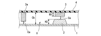
- this conventional method for example, as shown in FIG.
- a clearance (hereinafter, referred to as a peripheral clearance) Cb is also formed on the peripheral side of the sex part 3 and the gap reference part 3a. Then, on the inner wall surface side of the housing member 1, a convex portion so that component clearance Ca with the heat generating component 3 can be secured at a position facing the heat generating component 3 whose height is smaller than the gap reference component 3a. 2 will be provided.
- the height H2 of the convex portion is set by calculating a dimension obtained by subtracting the height H1 of the heat generating component 3 and the component clearance Ca from the peripheral clearance Cb.
- the area of the peripheral clearance Cb is also present on the peripheral side of the heat generating component 3 whose height is lower than the gap reference part 3a, and the large hollow portion V is in the area of the peripheral clearance Cb. It will be formed.
- the hollow portion V is a mere air or the like, and the thermal conductivity is poor compared to the housing member 1 and the like. Therefore, if the volume of the hollow portion V is large, there is a possibility that the heat radiation performance may be deteriorated.
- component clearance Ca may be secured between the heat generating component 3 and the inner wall surface of the recess 5.
- the recessed portion 5 may not only be formed to face the heat-generating component 3 as described above, but also may be formed at a position facing to other various electronic components (the gap reference component 3a etc.).
- the gap reference component 3a the gap reference component 3a etc.
- the peripheral clearance Cb can be further narrowed.
- the peripheral clearance Cb according to the present embodiment is smaller than the peripheral clearance Cb set according to the height of the gap reference part 3a as in the conventional method, and a hollow portion which may be formed in the region of the peripheral clearance Cb The capacity of V can be reduced, and the heat dissipation can be improved.
- the recess of the present embodiment may be formed at each position facing the heat generating component on the inner wall surface side of the housing member, and one recess may be formed with respect to a plurality of heat generating components (heat generating components etc. close to each other). You may form a part, but according to the shape, size, height, mounting position, etc. of those heat-generating parts, the shape, size, depth, formation location, etc. Is preferred.
- the opening shape and the bottom wall shape of the recess are the cross section of the heat generating component To be larger than the shape (cross-sectional shape of the portion to be covered) and to ensure the desired component clearance between the heat-generating component located in the recess and the inner wall surface (bottom wall etc.) of the recess It can be set to. Furthermore, by making the side wall surface of the inner wall surface tapered, a recessed portion having an opening area larger than the bottom wall area may be formed.
- a partition wall formed protruding from the recessed portion in the direction between the heat generating components is interposed (a clearance is provided to prevent contact with each heat generating component). It may be provided and interposed). According to such a configuration, a part of the casing member (that is, the partition wall) can be brought close to each other between the heat generating components, and the heat dissipation can be further improved.
- the shape of the bottom wall surface of the recess is limited to a flat one.
- the heights of the respective heat generating components are different from each other, it can be mentioned that they are formed in a step-like shape in accordance with the respective heights to secure the component clearance.
- a heat dissipating material may be disposed in the component clearance between the inner wall surface of the recessed portion and the heat generating component.
- this heat dissipating material any material that is used in the field of electronic control devices can be appropriately applied.
- a heat dissipating material made of a silicon-based resin material and having elasticity in gel form can be mentioned. In addition to having elasticity as described above, it has, for example, adhesiveness and is interposed in a gap to prevent positional displacement, outflow, etc., and has environmental resistance and can maintain heat dissipation for a long time It is preferable to apply the above.
- the heat dissipating material disposed in the component clearance is surrounded by the inner wall surface of the recessed portion, it is possible to suppress the heat dissipating material from being displaced or flowing out of the component clearance.
- the recessed part in this embodiment is not limited to the position which opposes a heat-emitting component, for example, the location which opposes electronic components (henceforth a non-heat-emitting component) other than a heat-emitting component. It may also be formed. As a result, even if the non-heat-generating component has a relatively high height, it becomes easy to secure the component clearance associated with the non-heat-generating component, and it becomes easy to narrow the peripheral clearance. It is not necessary to interpose the heat sink in the component clearance of this non-heat generating component.
- the shape and the like are not particularly limited on the outer wall surface side of the housing member in which the recessed portion is formed, but the shape reflecting the recessed portion and the like on the inner wall surface side may be mentioned.
- the outer wall surface side in the part in which the concave part of the housing member was formed is made convex, and the outer wall surface side in the area
- the heat dissipating fins for example, pin-like or strip-like heat dissipating fins projecting from the bottom of the recess
- the heat dissipating fins are provided on the outer wall surface side of the housing member, the heat dissipating surface area can be increased and heat can be more easily dissipated. .
- the shape of the heat dissipating fins is not particularly limited.
- the appearance of the casing can be improved by adjusting the heights of the heat dissipating fins to one another, or electronic It is possible to improve the heat dissipation without increasing the size of the control device.
- the material to be applied to the housing member is not particularly limited, but it is preferable to apply a material having a high thermal conductivity to the housing member forming the recess, for example, a metal material (aluminum, iron, etc. And the like are integrally molded into a desired shape by a molding method and a casting method (such as die casting). Further, for the purpose of enhancing the thermal emissivity from the surface of the housing member, for example, the surface of the housing member may be subjected to insulation processing of a thin film (for example, surface processing such as alumite or painting processing such as cationic electrodeposition).
- component clearances and peripheral clearances are appropriately formed in consideration of the amount of deformation. For example, even if the amount of deformation at a position close to the fixing point of the housing member or the circuit board is relatively small, the amount of deformation at other points (positions separated from the fixing point) seems to be relatively large. . Therefore, it is conceivable to make the component clearance and the peripheral clearance sufficiently large in accordance with the distance from the fixing point.
- a breathing filter for the housing member and the circuit board.
- a breathing filter may be provided on the peripheral side of the recess in the casing member facing the heat generating component.
- the heat-generating component becomes a high-temperature heat generation region, so a so-called breathing filter is provided to the casing member facing the heat generation region.
- the respiratory filter itself is not particularly limited, and a so-called snap fit type, a welded type (sealed type) or the like can be applied as appropriate.
- the heat-generating component and the non-heat-generating component are mounted at a predetermined distance from each other, and the peripheral clearance is formed as described above, so that the heat-generating component is thermally isolated from the non-heat-producing component. It is possible to
- FIGS. 1 to 4 for convenience, the description of the concave portion, the heat generating component, the heat dissipating material and the like will be omitted as appropriate, and will be described in the following embodiment.
- the electronic control unit 10 includes a housing formed by liquid-tightly joining (joining via a sealing material) a substantially plate-like case 12 attached to a vehicle body side and a substantially box-like cover 13, and the inside of the case
- the circuit board 4 is roughly composed of a circuit board 4 which is housed in a protective space and mounted with various electronic parts (heat generation parts 3 and non-heat generation parts 14b etc. described later).
- the bracket 12 is mounted on the vehicle body side.
- the mounting surface on the vehicle body side is configured parallel to the bottom surface of the case 12 in this embodiment, the mounting surface (brackets 23 and 24) on the vehicle body side may face the bottom surface of the case 12 May be inclined.
- the circuit board 4 does not generate heat relatively, such as a capacitor, a coil, etc., on its upper side surface (surface on the cover 13 side) 4a, or special heat radiation such as a heat sink, for example.
- Non-heat-generating parts 14b which do not require treatment are mounted, and so-called heat-generating parts 3 relatively easy to generate heat, such as arithmetic processing units, transistors and ICs, are mounted on the lower side surface (surface on case 12 side) 4b
- a wiring circuit pattern is formed on a front surface or a back surface of a plate material made of, for example, glass epoxy resin or the like, or in the inside, and the heat generating component 3 and the non-heat generating component 14b are respectively electrically It is connected to the.
- a connector 15 having two first and second connection ports 16 and 17 respectively connected to an external connector is attached to a part of the peripheral side of the circuit board 4.
- the connector 15 is one in which the respective connection ports 16 and 17 divided into two according to the connection destination are integrated through the mounting base 15a, and the circuit board 4 is formed through the mounting base 15a. It is fixed (for example, fixed by a plurality of screws or the like).
- a series of connection ports 16 and 17 connected by the mounting base 15a is exposed to the outside through a window 13a which is a space formed between the case 12 and the cover 13. Is connected to the connector on the vehicle side.
- the connector 15 is provided with a plurality of male terminals 16a and 17a electrically connected to the wiring circuit pattern on the circuit board 4, and these male terminals 16a and 17a are accommodated in a connector not shown. By being connected to the plurality of female terminals, it is electrically connected to predetermined devices such as sensors and pumps connected to the connector (female terminal) outside the figure.
- the case 12 is integrally formed in a substantially plate shape, more specifically, in a shallow box shape having a slightly rising peripheral edge, by a metal material having excellent thermal conductivity such as aluminum.
- side walls 12b are erected on the outer peripheral edge (each side) of the substantially rectangular bottom wall 12a, and the whole is configured to open upward.
- cover fixing portions 28 for mounting and fixing the cover 13 are formed, and through holes 28a penetrating in the vertical direction are provided in the respective cover fixing portions 28.
- the mounting and fixing of the circuit board 11 is performed via a board fixing portion 19 erected at the peripheral edge portion on the inner wall surface side of the bottom wall 12 a of the case 12.
- a flat support surface for supporting the circuit board 4 is formed at the upper end portion of the substrate fixing portion 19, and screws (not shown) for fixing the circuit substrate 4 are screwed on these support surfaces.
- a female screw hole 19a is formed. By screwing a screw into each female screw hole 19 a, the circuit board 4 is fixed to the case 12 in a state of being supported by each board fixing portion 19.
- a pair of brackets 23 and 24 which are used to attach the electronic control device 10 to a vehicle body (not shown) are integrally provided on the outer side portion of the side wall 12 b in the case 12.
- the brackets 23 and 24 are provided with a through hole 23a penetrating vertically and a notched groove 24a opened to the side respectively, and a bolt or the like inserted through the through hole 23a and the notched groove 24a to the vehicle side Installation is done.
- a plurality of strip-shaped radiation fins 12 c are provided on the outer wall surface 12 b on the lower side of the bottom wall 12 a in the case 12. It is provided in parallel at predetermined intervals.
- the cover 13 is integrally molded in a substantially box shape with a predetermined synthetic resin material at a lighter weight and at a lower cost than a metal material, and covers the upper wall portion 25 covering the upper side of the circuit board 4 and the connector 15; And a side wall 26 surrounding three sides of the peripheral edge of the upper wall 25 except the window 13a.
- a material (synthetic resin material etc.) different from the material (metal material etc.) of the case 12 may be applied, but the same material as the material of the case 12 You may apply a thing.
- Positioning protrusions 27a having a shape capable of penetrating through the through holes 28a of the cover fixing portion 28 are formed at positions on the side wall 26 facing the cover fixing portions 28 of the case 12, and the positioning protrusions 27a are respectively formed
- the cover 13 is fixed to the case 12 while being supported by the cover fixing portions 28 by being inserted into the through holes 28 a.
- the joint portion between the upper peripheral edge of the case 12 and the lower peripheral edge of the cover 13, the joint portion between the upper peripheral edge of the case 12 and the lower peripheral edge of the connector 15, and the outer periphery of the connector 15 are respectively liquid-tightly joined via a sealing agent in order to ensure waterproofness.
- a seal structure in which a flat seal is formed can be configured to obtain a desired sealability.
- by forming a seal groove in one of the joint portions or providing a protrusion on the other, and inserting this protrusion into the seal groove with a gap the gap between the seal groove and the protrusion is filled.
- the length of the sealing agent that is, the so-called seal length can be sufficiently secured to obtain the desired sealability.
- the sealing agent the specific configuration is not particularly limited as long as it is a flowable sealing agent, and for example, the specifications and requirements of the electronic control device 10 such as epoxy type, silicone type, acrylic type, etc. It can be appropriately selected accordingly.
- the connector 15 which is opened to the side is attached to one end of the circuit board 4.
- the cover 13 has a stepped shape corresponding to each of the circuit board 4 and the connector 15 having different dimensions (heights) in the thickness direction of the substrate.
- the upper wall portion 25 of the cover opposite to the case 12 with the circuit board 4 and the connector 15 interposed therebetween is provided with an upper portion 29 and a lower portion 30 parallel to the mounting surface 19 of the case 12 .
- the upper portion 29 covering the upper side of the connector 15 has a dimension in the substrate thickness direction set larger than the lower portion 30 covering the upper side of the circuit board 4.
- the inclined wall part 31 which smoothly connects the upper stage part 29 and the lower stage part 30 which differ in height in this way is provided.
- the inclined wall portion 31 is flatly inclined with respect to the bottom wall 12 a of the case 12 at a predetermined inclination angle, for example, an inclination angle of about 45 degrees, and therefore the same applies to the upper portion 29 and the lower portion 30. It is inclined at an inclination angle.
- a protective wall 33 is provided on the inclined wall portion 31 in order to protect a vent 32 formed to penetrate in the thickness direction for the purpose of forming a so-called respiratory filter.
- the vent hole 32 is attached with a thin film-like waterproof membrane (not shown) such as Gore-Tex (registered trademark) having both waterproofness and breathability. It is protected that high temperature, high pressure water does not spray directly on the ventilation waterproof membrane.
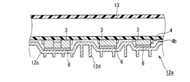
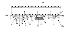
- FIG. 5 (a part of a cross section taken along the line X-X in FIG. 3 and the heat radiation fin 12c is omitted for convenience) is for explaining an example of the electronic control device in which the recessed portion is formed.
- a plurality of heat generating components 3 having different heights are mounted on the (surface on the case 13 side) 4b. Further, on the side of the inner wall surface 12 e of the bottom wall 12 a of the case 12, concave portions 5 are respectively formed at positions facing the heat generating component 3.
- the side wall surface 5b is formed in a tapered shape, and the outer wall side of the heat generating component 3 is covered with the inner wall surface 5a.
- a component clearance Ca of a desired size is provided between the inner wall surface 5a of the recessed portion 5 and the heat generating component 3, and the lower side surface 4b and the bottom wall 12a of the circuit board 4 on the peripheral side of the recessed portion 5
- a peripheral clearance Cb is provided between the inner wall surface 12d of the second embodiment.
- the heat sink 6 may be appropriately interposed at the part clearance Ca, for example, as shown in the figure, it may be interposed between the tip of the heat generating part 3 and the bottom wall surface 5c in the recessed part 5
- the heat dissipating material 6 may be filled in the recessed portion 5 to fill the hole.
- the surface of the recessed portion 5 may be subjected to insulation treatment of a thin film (for example, surface treatment such as alumite or painting treatment such as cationic electrodeposition).
- the peripheral clearance on the peripheral side of the heat generating component 3 can be narrowed, and the heat generating component 3
- the heat from the heat source can be easily conducted to the case 12 side, and the heat dissipation can be improved.
- the heat dissipation material is interposed in the recessed portion 5, the heat dissipation material is surrounded by the inner wall surface 5a of the recessed portion 5, so that the positional displacement and the outflow of the heat dissipation material can be suppressed. It is possible to suppress the cost increase.
- Example 2 6 and 7 are schematic views for explaining a modification of the first embodiment.
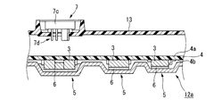
- FIG. 6 shows an example in which a welded-type (seal-type) respiratory filter 7 is provided on the cover 13, and the heat generation portion (upper side surface) of the circuit board 4 on the upper side (back side) of the heat generating component 3 It is provided at a position opposite to 4a).
- the respiratory filter 7 includes a vent 7a formed in the cover 13 and a thin film-like waterproof membrane 7b attached to the vent 7a.
- FIG. 7 shows an example in which a snap-fit type breathing filter 7 is provided, and a filter body 7c having breathability and waterproofness, and the filter body 7c are covered by a so-called snap-fit method. And a snap fit portion 7d which engages with and holds.
- the breathing filter 7 as shown in FIGS. 6 and 7, for example, the heat present between the circuit board 4 and the cover 13 without being dissipated from the recess 5 can be transferred to the outside of the casing by the breathing filter 7. It becomes easy to radiate heat, and it becomes possible to aim at the improvement of heat dissipation.
- Example 3 8 and 9 are schematic views for explaining a modification of the second embodiment.
- a welded (sealed) type breathing filter 7 is provided at the position of the area of the peripheral clearance Cb in the bottom wall 12a. It is provided.
- FIG. 9 shows an example in which a snap-fit type breathing filter 7 is provided, and is provided at the position of the region of the peripheral clearance Cb in the bottom wall 12a as in FIG.
- the heat present in the region of the peripheral clearance Cb without being dissipated from the recess 5 can be easily dissipated to the outside of the casing by the breathing filter 7. It is possible to improve the heat dissipation.
- FIG. 10 is a schematic view for explaining a modification of the first embodiment, and shows an example of setting the component clearance on the assumption that the casing member and the circuit board may be deformed.
- the component clearances Ca1 to Ca3 with respect to the sex component 3 are set to satisfy the relational expression of Ca1>Ca2> Ca3, and are set to sequentially increase as the distance from the substrate fixing portion 19 increases.
- the bottom wall 12a or the circuit board 4 is deformed according to the deformation due to thermal deformation or the like. Necessary and sufficient component clearance can be maintained, for example, it can be suppressed so that the exothermic component 3 and the bottom wall 12a do not interfere with each other without increasing the hollow portion in the peripheral clearance region, and the heat dissipation can be improved. It becomes possible.
- Example 5 11 and 12 are schematic diagrams for explaining a modification of the fourth embodiment, and the heat-generating component 3 is mounted on a predetermined region and other electronic components are mounted. This is an example of the case where the distance is separated from (non-heat-generating component etc.), and the heat-generating component 3 is mounted on a region of the circuit board 4 close to the substrate fixing portion 19 and mounted A recessed portion 5, a component clearance Ca and a radiation fin 12c are provided according to the heat generating component 3.
- the heat generating component 3 By mounting the heat generating component 3 as shown in FIG. 11 and FIG. 12, it is possible to separate the distance (distance due to wide peripheral clearance) with other electronic components, and the heat from the heat generating component It can be suppressed so as not to affect other electronic components. Further, by mounting in a region close to the substrate fixing portion 19, it is possible to suppress the heat generation component 3 and the bottom wall 12a from interfering with each other, for example, without increasing the hollow portion in the peripheral clearance region. It is possible to improve.
Landscapes
- Engineering & Computer Science (AREA)
- Microelectronics & Electronic Packaging (AREA)
- Physics & Mathematics (AREA)
- Thermal Sciences (AREA)
- Cooling Or The Like Of Electrical Apparatus (AREA)
- Cooling Or The Like Of Semiconductors Or Solid State Devices (AREA)
Abstract
Description
以下に、本実施形態に係る電子制御装置を、自動車のエンジンコントロールユニットに適用した一例について、図面に基づいて詳細に説明する。先ず、図1~図4を参照して、複数の筐体部材(後述するケース12,カバー13等)を接合して成る筐体内部の空間に回路基板4を収容した電子制御装置10の基本構成について説明する。なお、ここでの説明においては、便宜上、図1の上下方向、つまり回路基板4の肉厚方向を装置10自体の上下方向として説明することがあるが、これは、車載状態での鉛直方向に必ずしも対応するものではなく、例えば車両搭載状態が縦置き姿勢の場合、図1の装置10の上下方向が自動車の前後方向に沿うものとなる。また、図1~図4では便宜上、凹陥部,発熱性部品,放熱材等の説明を適宜省略し、後述の実施例で説明する。
図5(図3のX-X断面の一部。なお、放熱フィン12cは便宜上省略)は、凹陥部を形成した電子制御装置の一例を説明するためのものであり、回路基板4の下方側面(ケース13側の面)4bに、それぞれ高さの異なる複数個の発熱性部品3が実装されている。また、ケース12の底壁12aの内壁面12e側においては、発熱性部品3に対向する位置に凹陥部5がそれぞれ形成されている。これら凹陥部5は、その内壁面5aのうち側壁面5bがテーパー状に成形され、当該内壁面5aによって発熱性部品3の外周側を包覆している。また、凹陥部5の内壁面5aと発熱性部品3との間には所望の大きさの部品クリアランスCaが設けられ、その凹陥部5の周縁側で回路基板4の下方側面4bと底壁12aの内壁面12dとの間には周縁クリアランスCbが設けられている。
図6,図7は実施例1の変形例を説明するための概略図である。図6においては、カバー13に溶着型(シール型)の呼吸フィルタ7を設けた一例を示すものであって、回路基板4における発熱性部品3の上方側(裏面側)の発熱部位(上方側面4a)に対向した位置に設けられている。この呼吸フィルタ7は、カバー13に形成された通気孔7aと、その通気孔7aに取り付けられた薄膜状の通気防水膜7bと、を具備している。また、図7においては、スナップフィット型の呼吸フィルタ7を設けた一例を示すものであって、通気性,防水性を備えたフィルタ本体7cと、そのフィルタ本体7cを所謂スナップフィット方式によりカバー13に対して係合保持するスナップフィット部7dと、を具備して成る。
図8,図9は実施例2の変形例を説明するための概略図であり、図8においては、底壁12aにおける周縁クリアランスCbの領域の位置に溶着型(シール型)の呼吸フィルタ7が設けられている。また、図9においては、スナップフィット型の呼吸フィルタ7を設けた一例を示すものであって、図8同様に底壁12aにおける周縁クリアランスCbの領域の位置に設けられている。
図10は、実施例1の変形例を説明するための概略図であり、筐体部材や回路基板が変形し得ることを想定して部品クリアランスを設定する一例を示すものであって、各発熱性部品3に対するそれぞれの部品クリアランスCa1~Ca3がCa1>Ca2>Ca3の関係式を満たすようにし、基板固定部19から距離を隔てた箇所になるに連れて順次大きくなるように設定している。
図11,図12(図11のY-Y断面の一部)は、実施例4の変形例を説明するための概略図であり、発熱性部品3を所定の領域に実装し他の電子部品(非発熱性部品等)から距離を隔てるようにした場合の一例を示すものであって、発熱性部品3が回路基板4における基板固定部19に近接した領域に対して実装し、その実装された発熱性部品3に応じて凹陥部5,部品クリアランスCa,放熱フィン12cが設けられている。
Claims (3)
- 複数の筐体部材を接合してなる筐体内部の空間に、発熱する発熱性電子部品を一つ以上実装した回路基板が収容された電子制御装置であって、
前記発熱性電子部品に対向した筐体部材は、その発熱性電子部品が対向する位置に凹陥部が形成された電子制御装置。 - 前記凹陥部と発熱性電子部品との間に放熱材が介在した請求項1記載の電子制御装置。
- 前記発熱性電子部品の少なくとも一部が、凹陥部の内壁面により包覆されている請求項1記載の電子制御装置。
Priority Applications (5)
| Application Number | Priority Date | Filing Date | Title |
|---|---|---|---|
| CN201380044996.XA CN104663010B (zh) | 2012-09-21 | 2013-09-12 | 电子控制装置 |
| DE112013004625.3T DE112013004625T5 (de) | 2012-09-21 | 2013-09-12 | Elektronische Steuerungsvorrichtung |
| US14/424,099 US9480189B2 (en) | 2012-09-21 | 2013-09-12 | Electronic control apparatus |
| MX2015002743A MX340396B (es) | 2012-09-21 | 2013-09-12 | Aparato de control electrónico. |
| IN1579DEN2015 IN2015DN01579A (ja) | 2012-09-21 | 2013-09-12 |
Applications Claiming Priority (2)
| Application Number | Priority Date | Filing Date | Title |
|---|---|---|---|
| JP2012-208927 | 2012-09-21 | ||
| JP2012208927A JP2014063930A (ja) | 2012-09-21 | 2012-09-21 | 電子制御装置 |
Publications (1)
| Publication Number | Publication Date |
|---|---|
| WO2014046004A1 true WO2014046004A1 (ja) | 2014-03-27 |
Family
ID=50341318
Family Applications (1)
| Application Number | Title | Priority Date | Filing Date |
|---|---|---|---|
| PCT/JP2013/074678 Ceased WO2014046004A1 (ja) | 2012-09-21 | 2013-09-12 | 電子制御装置 |
Country Status (7)
| Country | Link |
|---|---|
| US (1) | US9480189B2 (ja) |
| JP (1) | JP2014063930A (ja) |
| CN (1) | CN104663010B (ja) |
| DE (1) | DE112013004625T5 (ja) |
| IN (1) | IN2015DN01579A (ja) |
| MX (1) | MX340396B (ja) |
| WO (1) | WO2014046004A1 (ja) |
Cited By (4)
| Publication number | Priority date | Publication date | Assignee | Title |
|---|---|---|---|---|
| TWI718980B (zh) * | 2020-08-07 | 2021-02-11 | 新唐科技股份有限公司 | 整合式感測裝置與其製造方法 |
| JPWO2021059914A1 (ja) * | 2019-09-25 | 2021-04-01 | ||
| WO2025005087A1 (ja) * | 2023-06-26 | 2025-01-02 | 積水化学工業株式会社 | 筐体構造及びその製造方法 |
| WO2025104867A1 (ja) * | 2023-11-16 | 2025-05-22 | Astemo株式会社 | 電子制御装置 |
Families Citing this family (27)
| Publication number | Priority date | Publication date | Assignee | Title |
|---|---|---|---|---|
| TWI543546B (zh) * | 2012-12-11 | 2016-07-21 | 和佐公司 | 具有通汽口之電子裝置及其外殼 |
| JP6398849B2 (ja) * | 2015-04-06 | 2018-10-03 | 株式会社デンソー | 電子制御装置 |
| DE102015107645A1 (de) * | 2015-05-15 | 2016-11-17 | Hella Kgaa Hueck & Co. | Sensorgehäuse für einen Radardensor und Radarsensor |
| DE102015212616A1 (de) * | 2015-07-06 | 2017-01-12 | Zf Friedrichshafen Ag | Schutzgehäuse zur flexiblen Bauteilfixierung und Leiterplatte mit Schutzgehäuse |
| CN105163544A (zh) * | 2015-09-22 | 2015-12-16 | 武汉菱电汽车电控系统股份有限公司 | 多功能汽车电子控制单元封装盒 |
| JP6453195B2 (ja) * | 2015-09-29 | 2019-01-16 | 日立オートモティブシステムズ株式会社 | 車載制御装置 |
| DE102015221149A1 (de) * | 2015-10-29 | 2017-05-04 | Robert Bosch Gmbh | Steuervorrichtung für eine Getriebesteuerung eines Kraftfahrzeugs |
| JP2017098332A (ja) * | 2015-11-19 | 2017-06-01 | 株式会社ジェイテクト | 電子回路装置 |
| CN105374769A (zh) * | 2015-12-04 | 2016-03-02 | 重庆臻远电气有限公司 | 散热装置 |
| US10164362B2 (en) * | 2015-12-31 | 2018-12-25 | Foxconn Interconnect Technology Limited | Plug connecetor with a metallic enclosure having heat sink member thereon |
| JP6424839B2 (ja) * | 2016-01-08 | 2018-11-21 | 株式会社デンソー | 電子制御ユニット、および、これを用いた電動パワーステアリング装置 |
| JP6113314B1 (ja) * | 2016-02-01 | 2017-04-12 | 三菱電機株式会社 | 防水型制御装置 |
| JP6565757B2 (ja) * | 2016-03-25 | 2019-08-28 | 株式会社デンソー | 電子装置 |
| DE102017212968B4 (de) * | 2016-08-05 | 2024-02-01 | Robert Bosch Gmbh | Gehäuseaufbau für eine elektronische steuereinheit und herstellungsverfahren |
| JP6499213B2 (ja) * | 2017-02-17 | 2019-04-10 | 太陽誘電株式会社 | カバー及びそれを用いたモジュール |
| US10638643B2 (en) * | 2017-11-14 | 2020-04-28 | Canon Kabushiki Kaisha | Electronic device |
| US11375639B2 (en) * | 2018-06-03 | 2022-06-28 | Tcpoly Inc. | Additive manufactured multi-layer thermally conductive parts |
| US10813240B2 (en) | 2018-12-05 | 2020-10-20 | Carrier Corporation | Control box including a water resistant seal |
| JP7439468B2 (ja) * | 2019-11-20 | 2024-02-28 | 富士電機株式会社 | プログラマブルコントローラモジュール及びプログラマブルコントローラシステム |
| JP7536631B2 (ja) * | 2020-12-18 | 2024-08-20 | 株式会社マキタ | 電動作業機 |
| DE102021000931A1 (de) | 2021-02-22 | 2022-08-25 | KSB SE & Co. KGaA | Pumpe mit einem Elektronikgehäuse und wenigstens einem Kühlkörper |
| CN116636312B (zh) * | 2021-03-10 | 2026-06-09 | 日立安斯泰莫株式会社 | 电子控制装置 |
| DE102021001714A1 (de) | 2021-04-01 | 2022-10-06 | KSB SE & Co. KGaA | Kreiselpumpe mit Kühlung der Elektronik innerhalb eines Elektronikgehäuses |
| JP7606676B2 (ja) * | 2021-06-11 | 2024-12-26 | 株式会社オートネットワーク技術研究所 | 回路構成体 |
| JP2023130256A (ja) * | 2022-03-07 | 2023-09-20 | 株式会社デンソーテン | 電子機器 |
| CN116919010A (zh) * | 2022-04-02 | 2023-10-24 | 深圳麦克韦尔科技有限公司 | 电子雾化装置及其雾化器 |
| JP7744110B2 (ja) * | 2023-05-15 | 2025-09-25 | 矢崎総業株式会社 | 電気接続箱、及び、ワイヤハーネス |
Citations (3)
| Publication number | Priority date | Publication date | Assignee | Title |
|---|---|---|---|---|
| JP2009054701A (ja) * | 2007-08-24 | 2009-03-12 | Hitachi Kokusai Electric Inc | 電子部品放熱構造 |
| WO2010067725A1 (ja) * | 2008-12-12 | 2010-06-17 | 株式会社 村田製作所 | 回路モジュール |
| JP2011192937A (ja) * | 2010-03-17 | 2011-09-29 | Hitachi Automotive Systems Ltd | 自動車用電子制御装置 |
Family Cites Families (27)
| Publication number | Priority date | Publication date | Assignee | Title |
|---|---|---|---|---|
| DE19609845C1 (de) * | 1996-03-13 | 1997-05-28 | Loh Kg Rittal Werk | Kühlgerät zum Anbau an die Rückwand, Seitenwand oder Tür eines Schaltschrankes |
| US6198631B1 (en) * | 1999-12-03 | 2001-03-06 | Pass & Seymour, Inc. | High temperature ground connection |
| JP2005117887A (ja) * | 2003-09-19 | 2005-04-28 | Auto Network Gijutsu Kenkyusho:Kk | 車載用回路ユニットの取付構造及び車載用回路ユニット |
| US6903936B2 (en) * | 2003-10-28 | 2005-06-07 | Saul Lin | Power regulator |
| US7621723B2 (en) * | 2004-03-22 | 2009-11-24 | Shinano Kenshi Kabushiki Kaisha | Electromagnetic pump |
| JP2005282715A (ja) * | 2004-03-30 | 2005-10-13 | Denso Corp | 制御装置 |
| US20050286223A1 (en) * | 2004-06-24 | 2005-12-29 | Morales Ralph G | Electronic device baffle |
| US7400239B2 (en) * | 2004-09-03 | 2008-07-15 | Simply Automated, Incorporated | Universal control apparatus and methods |
| DE112005002218T5 (de) * | 2004-09-17 | 2007-08-09 | Kabushiki Kaisha Yaskawa Denki, Kitakyushu | Motorsteuervorrichtung und Verfahren zum Montieren der Motorsteuervorrichtung |
| US7130196B2 (en) * | 2005-01-19 | 2006-10-31 | General Electric Company | Apparatus and method for transferring heat from control devices |
| JP4538359B2 (ja) * | 2005-03-31 | 2010-09-08 | 株式会社日立産機システム | 電気回路モジュール |
| EP1732375B1 (de) * | 2005-06-10 | 2009-08-26 | ebm-papst St. Georgen GmbH & Co. KG | Gerätelüfter |
| JP4593416B2 (ja) | 2005-09-22 | 2010-12-08 | 株式会社デンソー | 電子制御装置 |
| US20070165376A1 (en) * | 2006-01-17 | 2007-07-19 | Norbert Bones | Three phase inverter power stage and assembly |
| JP4278680B2 (ja) * | 2006-12-27 | 2009-06-17 | 三菱電機株式会社 | 電子制御装置 |
| JP4410242B2 (ja) * | 2006-12-27 | 2010-02-03 | 三菱電機株式会社 | 電子制御装置及びその製造方法 |
| US7477513B1 (en) * | 2006-12-29 | 2009-01-13 | Isothermal Systems Research, Inc. | Dual sided board thermal management system |
| JP4385058B2 (ja) * | 2007-05-07 | 2009-12-16 | 三菱電機株式会社 | 電子制御装置 |
| WO2008146845A1 (ja) * | 2007-05-28 | 2008-12-04 | Aisin Aw Co., Ltd. | 自動変速機用コントロールユニット冷却装置 |
| US20090201641A1 (en) * | 2008-02-13 | 2009-08-13 | Inventec Corporation | Airflow conducting structure |
| JP4510926B2 (ja) * | 2008-11-05 | 2010-07-28 | 三菱電機株式会社 | 強制風冷式車両用制御装置 |
| JP5344182B2 (ja) * | 2010-02-02 | 2013-11-20 | 株式会社安川電機 | 電力変換装置 |
| JP4948613B2 (ja) * | 2010-02-25 | 2012-06-06 | 三菱電機株式会社 | 樹脂封止形電子制御装置、及びその製造方法 |
| DE102011012673A1 (de) | 2010-03-17 | 2011-09-22 | Hitachi Automotive Systems, Ltd. | Elektronische Steuereinrichtung für Fahrzeuge |
| JP5557585B2 (ja) * | 2010-04-26 | 2014-07-23 | 日立オートモティブシステムズ株式会社 | パワーモジュール |
| US8427091B2 (en) * | 2011-03-09 | 2013-04-23 | Hiwin Mikrosystem Corp. | Drive with heat dissipation and energy-saving function |
| JP5614542B2 (ja) * | 2011-03-28 | 2014-10-29 | 株式会社安川電機 | モータ制御装置 |
-
2012
- 2012-09-21 JP JP2012208927A patent/JP2014063930A/ja active Pending
-
2013
- 2013-09-12 US US14/424,099 patent/US9480189B2/en active Active
- 2013-09-12 DE DE112013004625.3T patent/DE112013004625T5/de not_active Ceased
- 2013-09-12 MX MX2015002743A patent/MX340396B/es active IP Right Grant
- 2013-09-12 WO PCT/JP2013/074678 patent/WO2014046004A1/ja not_active Ceased
- 2013-09-12 CN CN201380044996.XA patent/CN104663010B/zh active Active
- 2013-09-12 IN IN1579DEN2015 patent/IN2015DN01579A/en unknown
Patent Citations (3)
| Publication number | Priority date | Publication date | Assignee | Title |
|---|---|---|---|---|
| JP2009054701A (ja) * | 2007-08-24 | 2009-03-12 | Hitachi Kokusai Electric Inc | 電子部品放熱構造 |
| WO2010067725A1 (ja) * | 2008-12-12 | 2010-06-17 | 株式会社 村田製作所 | 回路モジュール |
| JP2011192937A (ja) * | 2010-03-17 | 2011-09-29 | Hitachi Automotive Systems Ltd | 自動車用電子制御装置 |
Cited By (5)
| Publication number | Priority date | Publication date | Assignee | Title |
|---|---|---|---|---|
| JPWO2021059914A1 (ja) * | 2019-09-25 | 2021-04-01 | ||
| WO2021059914A1 (ja) * | 2019-09-25 | 2021-04-01 | 日立Astemo株式会社 | 電子回路装置 |
| TWI718980B (zh) * | 2020-08-07 | 2021-02-11 | 新唐科技股份有限公司 | 整合式感測裝置與其製造方法 |
| WO2025005087A1 (ja) * | 2023-06-26 | 2025-01-02 | 積水化学工業株式会社 | 筐体構造及びその製造方法 |
| WO2025104867A1 (ja) * | 2023-11-16 | 2025-05-22 | Astemo株式会社 | 電子制御装置 |
Also Published As
| Publication number | Publication date |
|---|---|
| IN2015DN01579A (ja) | 2015-07-03 |
| CN104663010A (zh) | 2015-05-27 |
| MX2015002743A (es) | 2015-05-15 |
| US20150216088A1 (en) | 2015-07-30 |
| US9480189B2 (en) | 2016-10-25 |
| MX340396B (es) | 2016-07-07 |
| JP2014063930A (ja) | 2014-04-10 |
| DE112013004625T5 (de) | 2015-06-03 |
| CN104663010B (zh) | 2018-02-09 |
Similar Documents
| Publication | Publication Date | Title |
|---|---|---|
| CN104663010B (zh) | 电子控制装置 | |
| JP2013197405A (ja) | 電子制御装置 | |
| JP5358639B2 (ja) | 電子制御装置のシール構造 | |
| JP2014093414A (ja) | 電子制御装置 | |
| US11864362B2 (en) | Power supply device with a heat generating component | |
| US11076503B2 (en) | Thermally conductive insert element for electronic unit | |
| JP2010056493A (ja) | 電子制御装置 | |
| JP2019047049A (ja) | 半導体装置 | |
| JP2015198168A (ja) | 電子装置、電力変換装置及び回転電機 | |
| JP6303981B2 (ja) | 電気機器 | |
| CN102792034A (zh) | 用于连接电子组件和壳体部分的连接装置以及电子控制装置 | |
| JP6419125B2 (ja) | 電子制御装置 | |
| JP6588253B2 (ja) | 筐体構造体およびこれを用いた電子機器 | |
| JP2010225674A (ja) | 制御ユニット | |
| JP4450632B2 (ja) | 電力変換装置 | |
| WO2013084416A1 (ja) | 電力変換装置 | |
| WO2019031172A1 (ja) | 電力変換装置 | |
| JP2017126681A (ja) | 半導体ユニット | |
| JP7069734B2 (ja) | 電力変換装置 | |
| CN207249255U (zh) | 车用hud装置和车辆 | |
| JP5808703B2 (ja) | 電子制御装置 | |
| CN103999212B (zh) | 功率转换装置 | |
| CN104519720A (zh) | 框体及电器设备 | |
| JP2012199354A (ja) | 電子制御装置 | |
| JP6700978B2 (ja) | 電力変換装置 |
Legal Events
| Date | Code | Title | Description |
|---|---|---|---|
| 121 | Ep: the epo has been informed by wipo that ep was designated in this application |
Ref document number: 13839213 Country of ref document: EP Kind code of ref document: A1 |
|
| WWE | Wipo information: entry into national phase |
Ref document number: 14424099 Country of ref document: US |
|
| WWE | Wipo information: entry into national phase |
Ref document number: MX/A/2015/002743 Country of ref document: MX |
|
| WWE | Wipo information: entry into national phase |
Ref document number: 112013004625 Country of ref document: DE Ref document number: 1120130046253 Country of ref document: DE |
|
| 122 | Ep: pct application non-entry in european phase |
Ref document number: 13839213 Country of ref document: EP Kind code of ref document: A1 |