WO2014030414A1 - 成膜装置、低誘電率膜を形成する方法、SiCO膜、及びダマシン配線構造 - Google Patents
成膜装置、低誘電率膜を形成する方法、SiCO膜、及びダマシン配線構造 Download PDFInfo
- Publication number
- WO2014030414A1 WO2014030414A1 PCT/JP2013/066731 JP2013066731W WO2014030414A1 WO 2014030414 A1 WO2014030414 A1 WO 2014030414A1 JP 2013066731 W JP2013066731 W JP 2013066731W WO 2014030414 A1 WO2014030414 A1 WO 2014030414A1
- Authority
- WO
- WIPO (PCT)
- Prior art keywords
- plasma generation
- generation chamber
- film
- processing chamber
- gas
- Prior art date
- Legal status (The legal status is an assumption and is not a legal conclusion. Google has not performed a legal analysis and makes no representation as to the accuracy of the status listed.)
- Ceased
Links
Images


Classifications
-
- H—ELECTRICITY
- H01—ELECTRIC ELEMENTS
- H01J—ELECTRIC DISCHARGE TUBES OR DISCHARGE LAMPS
- H01J37/00—Discharge tubes with provision for introducing objects or material to be exposed to the discharge, e.g. for the purpose of examination or processing thereof
- H01J37/32—Gas-filled discharge tubes
- H01J37/32431—Constructional details of the reactor
- H01J37/32623—Mechanical discharge control means
- H01J37/32651—Shields, e.g. dark space shields, Faraday shields
-
- C—CHEMISTRY; METALLURGY
- C01—INORGANIC CHEMISTRY
- C01B—NON-METALLIC ELEMENTS; COMPOUNDS THEREOF; METALLOIDS OR COMPOUNDS THEREOF NOT COVERED BY SUBCLASS C01C
- C01B32/00—Carbon; Compounds thereof
- C01B32/90—Carbides
- C01B32/907—Oxycarbides; Sulfocarbides; Mixture of carbides
-
- C—CHEMISTRY; METALLURGY
- C23—COATING METALLIC MATERIAL; COATING MATERIAL WITH METALLIC MATERIAL; CHEMICAL SURFACE TREATMENT; DIFFUSION TREATMENT OF METALLIC MATERIAL; COATING BY VACUUM EVAPORATION, BY SPUTTERING, BY ION IMPLANTATION OR BY CHEMICAL VAPOUR DEPOSITION, IN GENERAL; INHIBITING CORROSION OF METALLIC MATERIAL OR INCRUSTATION IN GENERAL
- C23C—COATING METALLIC MATERIAL; COATING MATERIAL WITH METALLIC MATERIAL; SURFACE TREATMENT OF METALLIC MATERIAL BY DIFFUSION INTO THE SURFACE, BY CHEMICAL CONVERSION OR SUBSTITUTION; COATING BY VACUUM EVAPORATION, BY SPUTTERING, BY ION IMPLANTATION OR BY CHEMICAL VAPOUR DEPOSITION, IN GENERAL
- C23C16/00—Chemical coating by decomposition of gaseous compounds, without leaving reaction products of surface material in the coating, i.e. chemical vapour deposition [CVD] processes
- C23C16/22—Chemical coating by decomposition of gaseous compounds, without leaving reaction products of surface material in the coating, i.e. chemical vapour deposition [CVD] processes characterised by the deposition of inorganic material, other than metallic material
- C23C16/30—Deposition of compounds, mixtures or solid solutions, e.g. borides, carbides, nitrides
- C23C16/32—Carbides
- C23C16/325—Silicon carbide
-
- C—CHEMISTRY; METALLURGY
- C23—COATING METALLIC MATERIAL; COATING MATERIAL WITH METALLIC MATERIAL; CHEMICAL SURFACE TREATMENT; DIFFUSION TREATMENT OF METALLIC MATERIAL; COATING BY VACUUM EVAPORATION, BY SPUTTERING, BY ION IMPLANTATION OR BY CHEMICAL VAPOUR DEPOSITION, IN GENERAL; INHIBITING CORROSION OF METALLIC MATERIAL OR INCRUSTATION IN GENERAL
- C23C—COATING METALLIC MATERIAL; COATING MATERIAL WITH METALLIC MATERIAL; SURFACE TREATMENT OF METALLIC MATERIAL BY DIFFUSION INTO THE SURFACE, BY CHEMICAL CONVERSION OR SUBSTITUTION; COATING BY VACUUM EVAPORATION, BY SPUTTERING, BY ION IMPLANTATION OR BY CHEMICAL VAPOUR DEPOSITION, IN GENERAL
- C23C16/00—Chemical coating by decomposition of gaseous compounds, without leaving reaction products of surface material in the coating, i.e. chemical vapour deposition [CVD] processes
- C23C16/22—Chemical coating by decomposition of gaseous compounds, without leaving reaction products of surface material in the coating, i.e. chemical vapour deposition [CVD] processes characterised by the deposition of inorganic material, other than metallic material
- C23C16/30—Deposition of compounds, mixtures or solid solutions, e.g. borides, carbides, nitrides
- C23C16/40—Oxides
- C23C16/401—Oxides containing silicon
-
- C—CHEMISTRY; METALLURGY
- C23—COATING METALLIC MATERIAL; COATING MATERIAL WITH METALLIC MATERIAL; CHEMICAL SURFACE TREATMENT; DIFFUSION TREATMENT OF METALLIC MATERIAL; COATING BY VACUUM EVAPORATION, BY SPUTTERING, BY ION IMPLANTATION OR BY CHEMICAL VAPOUR DEPOSITION, IN GENERAL; INHIBITING CORROSION OF METALLIC MATERIAL OR INCRUSTATION IN GENERAL
- C23C—COATING METALLIC MATERIAL; COATING MATERIAL WITH METALLIC MATERIAL; SURFACE TREATMENT OF METALLIC MATERIAL BY DIFFUSION INTO THE SURFACE, BY CHEMICAL CONVERSION OR SUBSTITUTION; COATING BY VACUUM EVAPORATION, BY SPUTTERING, BY ION IMPLANTATION OR BY CHEMICAL VAPOUR DEPOSITION, IN GENERAL
- C23C16/00—Chemical coating by decomposition of gaseous compounds, without leaving reaction products of surface material in the coating, i.e. chemical vapour deposition [CVD] processes
- C23C16/44—Chemical coating by decomposition of gaseous compounds, without leaving reaction products of surface material in the coating, i.e. chemical vapour deposition [CVD] processes characterised by the method of coating
- C23C16/448—Chemical coating by decomposition of gaseous compounds, without leaving reaction products of surface material in the coating, i.e. chemical vapour deposition [CVD] processes characterised by the method of coating characterised by the method used for generating reactive gas streams, e.g. by evaporation or sublimation of precursor materials
- C23C16/452—Chemical coating by decomposition of gaseous compounds, without leaving reaction products of surface material in the coating, i.e. chemical vapour deposition [CVD] processes characterised by the method of coating characterised by the method used for generating reactive gas streams, e.g. by evaporation or sublimation of precursor materials by activating reactive gas streams before their introduction into the reaction chamber, e.g. by ionisation or addition of reactive species
-
- C—CHEMISTRY; METALLURGY
- C23—COATING METALLIC MATERIAL; COATING MATERIAL WITH METALLIC MATERIAL; CHEMICAL SURFACE TREATMENT; DIFFUSION TREATMENT OF METALLIC MATERIAL; COATING BY VACUUM EVAPORATION, BY SPUTTERING, BY ION IMPLANTATION OR BY CHEMICAL VAPOUR DEPOSITION, IN GENERAL; INHIBITING CORROSION OF METALLIC MATERIAL OR INCRUSTATION IN GENERAL
- C23C—COATING METALLIC MATERIAL; COATING MATERIAL WITH METALLIC MATERIAL; SURFACE TREATMENT OF METALLIC MATERIAL BY DIFFUSION INTO THE SURFACE, BY CHEMICAL CONVERSION OR SUBSTITUTION; COATING BY VACUUM EVAPORATION, BY SPUTTERING, BY ION IMPLANTATION OR BY CHEMICAL VAPOUR DEPOSITION, IN GENERAL
- C23C16/00—Chemical coating by decomposition of gaseous compounds, without leaving reaction products of surface material in the coating, i.e. chemical vapour deposition [CVD] processes
- C23C16/44—Chemical coating by decomposition of gaseous compounds, without leaving reaction products of surface material in the coating, i.e. chemical vapour deposition [CVD] processes characterised by the method of coating
- C23C16/455—Chemical coating by decomposition of gaseous compounds, without leaving reaction products of surface material in the coating, i.e. chemical vapour deposition [CVD] processes characterised by the method of coating characterised by the method used for introducing gases into reaction chamber or for modifying gas flows in reaction chamber
- C23C16/45557—Pulsed pressure or control pressure
-
- C—CHEMISTRY; METALLURGY
- C23—COATING METALLIC MATERIAL; COATING MATERIAL WITH METALLIC MATERIAL; CHEMICAL SURFACE TREATMENT; DIFFUSION TREATMENT OF METALLIC MATERIAL; COATING BY VACUUM EVAPORATION, BY SPUTTERING, BY ION IMPLANTATION OR BY CHEMICAL VAPOUR DEPOSITION, IN GENERAL; INHIBITING CORROSION OF METALLIC MATERIAL OR INCRUSTATION IN GENERAL
- C23C—COATING METALLIC MATERIAL; COATING MATERIAL WITH METALLIC MATERIAL; SURFACE TREATMENT OF METALLIC MATERIAL BY DIFFUSION INTO THE SURFACE, BY CHEMICAL CONVERSION OR SUBSTITUTION; COATING BY VACUUM EVAPORATION, BY SPUTTERING, BY ION IMPLANTATION OR BY CHEMICAL VAPOUR DEPOSITION, IN GENERAL
- C23C16/00—Chemical coating by decomposition of gaseous compounds, without leaving reaction products of surface material in the coating, i.e. chemical vapour deposition [CVD] processes
- C23C16/44—Chemical coating by decomposition of gaseous compounds, without leaving reaction products of surface material in the coating, i.e. chemical vapour deposition [CVD] processes characterised by the method of coating
- C23C16/455—Chemical coating by decomposition of gaseous compounds, without leaving reaction products of surface material in the coating, i.e. chemical vapour deposition [CVD] processes characterised by the method of coating characterised by the method used for introducing gases into reaction chamber or for modifying gas flows in reaction chamber
- C23C16/45561—Gas plumbing upstream of the reaction chamber
-
- C—CHEMISTRY; METALLURGY
- C23—COATING METALLIC MATERIAL; COATING MATERIAL WITH METALLIC MATERIAL; CHEMICAL SURFACE TREATMENT; DIFFUSION TREATMENT OF METALLIC MATERIAL; COATING BY VACUUM EVAPORATION, BY SPUTTERING, BY ION IMPLANTATION OR BY CHEMICAL VAPOUR DEPOSITION, IN GENERAL; INHIBITING CORROSION OF METALLIC MATERIAL OR INCRUSTATION IN GENERAL
- C23C—COATING METALLIC MATERIAL; COATING MATERIAL WITH METALLIC MATERIAL; SURFACE TREATMENT OF METALLIC MATERIAL BY DIFFUSION INTO THE SURFACE, BY CHEMICAL CONVERSION OR SUBSTITUTION; COATING BY VACUUM EVAPORATION, BY SPUTTERING, BY ION IMPLANTATION OR BY CHEMICAL VAPOUR DEPOSITION, IN GENERAL
- C23C16/00—Chemical coating by decomposition of gaseous compounds, without leaving reaction products of surface material in the coating, i.e. chemical vapour deposition [CVD] processes
- C23C16/44—Chemical coating by decomposition of gaseous compounds, without leaving reaction products of surface material in the coating, i.e. chemical vapour deposition [CVD] processes characterised by the method of coating
- C23C16/455—Chemical coating by decomposition of gaseous compounds, without leaving reaction products of surface material in the coating, i.e. chemical vapour deposition [CVD] processes characterised by the method of coating characterised by the method used for introducing gases into reaction chamber or for modifying gas flows in reaction chamber
- C23C16/45563—Gas nozzles
- C23C16/45565—Shower nozzles
-
- C—CHEMISTRY; METALLURGY
- C23—COATING METALLIC MATERIAL; COATING MATERIAL WITH METALLIC MATERIAL; CHEMICAL SURFACE TREATMENT; DIFFUSION TREATMENT OF METALLIC MATERIAL; COATING BY VACUUM EVAPORATION, BY SPUTTERING, BY ION IMPLANTATION OR BY CHEMICAL VAPOUR DEPOSITION, IN GENERAL; INHIBITING CORROSION OF METALLIC MATERIAL OR INCRUSTATION IN GENERAL
- C23C—COATING METALLIC MATERIAL; COATING MATERIAL WITH METALLIC MATERIAL; SURFACE TREATMENT OF METALLIC MATERIAL BY DIFFUSION INTO THE SURFACE, BY CHEMICAL CONVERSION OR SUBSTITUTION; COATING BY VACUUM EVAPORATION, BY SPUTTERING, BY ION IMPLANTATION OR BY CHEMICAL VAPOUR DEPOSITION, IN GENERAL
- C23C16/00—Chemical coating by decomposition of gaseous compounds, without leaving reaction products of surface material in the coating, i.e. chemical vapour deposition [CVD] processes
- C23C16/44—Chemical coating by decomposition of gaseous compounds, without leaving reaction products of surface material in the coating, i.e. chemical vapour deposition [CVD] processes characterised by the method of coating
- C23C16/455—Chemical coating by decomposition of gaseous compounds, without leaving reaction products of surface material in the coating, i.e. chemical vapour deposition [CVD] processes characterised by the method of coating characterised by the method used for introducing gases into reaction chamber or for modifying gas flows in reaction chamber
- C23C16/45563—Gas nozzles
- C23C16/4558—Perforated rings
-
- C—CHEMISTRY; METALLURGY
- C23—COATING METALLIC MATERIAL; COATING MATERIAL WITH METALLIC MATERIAL; CHEMICAL SURFACE TREATMENT; DIFFUSION TREATMENT OF METALLIC MATERIAL; COATING BY VACUUM EVAPORATION, BY SPUTTERING, BY ION IMPLANTATION OR BY CHEMICAL VAPOUR DEPOSITION, IN GENERAL; INHIBITING CORROSION OF METALLIC MATERIAL OR INCRUSTATION IN GENERAL
- C23C—COATING METALLIC MATERIAL; COATING MATERIAL WITH METALLIC MATERIAL; SURFACE TREATMENT OF METALLIC MATERIAL BY DIFFUSION INTO THE SURFACE, BY CHEMICAL CONVERSION OR SUBSTITUTION; COATING BY VACUUM EVAPORATION, BY SPUTTERING, BY ION IMPLANTATION OR BY CHEMICAL VAPOUR DEPOSITION, IN GENERAL
- C23C16/00—Chemical coating by decomposition of gaseous compounds, without leaving reaction products of surface material in the coating, i.e. chemical vapour deposition [CVD] processes
- C23C16/44—Chemical coating by decomposition of gaseous compounds, without leaving reaction products of surface material in the coating, i.e. chemical vapour deposition [CVD] processes characterised by the method of coating
- C23C16/50—Chemical coating by decomposition of gaseous compounds, without leaving reaction products of surface material in the coating, i.e. chemical vapour deposition [CVD] processes characterised by the method of coating using electric discharges
- C23C16/511—Chemical coating by decomposition of gaseous compounds, without leaving reaction products of surface material in the coating, i.e. chemical vapour deposition [CVD] processes characterised by the method of coating using electric discharges using microwave discharges
-
- H—ELECTRICITY
- H01—ELECTRIC ELEMENTS
- H01J—ELECTRIC DISCHARGE TUBES OR DISCHARGE LAMPS
- H01J37/00—Discharge tubes with provision for introducing objects or material to be exposed to the discharge, e.g. for the purpose of examination or processing thereof
- H01J37/32—Gas-filled discharge tubes
- H01J37/32009—Arrangements for generation of plasma specially adapted for examination or treatment of objects, e.g. plasma sources
- H01J37/32192—Microwave generated discharge
- H01J37/32211—Means for coupling power to the plasma
- H01J37/3222—Antennas
-
- H—ELECTRICITY
- H01—ELECTRIC ELEMENTS
- H01J—ELECTRIC DISCHARGE TUBES OR DISCHARGE LAMPS
- H01J37/00—Discharge tubes with provision for introducing objects or material to be exposed to the discharge, e.g. for the purpose of examination or processing thereof
- H01J37/32—Gas-filled discharge tubes
- H01J37/32009—Arrangements for generation of plasma specially adapted for examination or treatment of objects, e.g. plasma sources
- H01J37/32192—Microwave generated discharge
- H01J37/32211—Means for coupling power to the plasma
- H01J37/32238—Windows
-
- H—ELECTRICITY
- H01—ELECTRIC ELEMENTS
- H01J—ELECTRIC DISCHARGE TUBES OR DISCHARGE LAMPS
- H01J37/00—Discharge tubes with provision for introducing objects or material to be exposed to the discharge, e.g. for the purpose of examination or processing thereof
- H01J37/32—Gas-filled discharge tubes
- H01J37/32431—Constructional details of the reactor
- H01J37/3244—Gas supply means
-
- H—ELECTRICITY
- H01—ELECTRIC ELEMENTS
- H01L—SEMICONDUCTOR DEVICES NOT COVERED BY CLASS H10
- H01L21/00—Processes or apparatus adapted for the manufacture or treatment of semiconductor or solid state devices or of parts thereof
- H01L21/02—Manufacture or treatment of semiconductor devices or of parts thereof
- H01L21/02104—Forming layers
- H01L21/02107—Forming insulating materials on a substrate
- H01L21/02109—Forming insulating materials on a substrate characterised by the type of layer, e.g. type of material, porous/non-porous, pre-cursors, mixtures or laminates
- H01L21/02112—Forming insulating materials on a substrate characterised by the type of layer, e.g. type of material, porous/non-porous, pre-cursors, mixtures or laminates characterised by the material of the layer
- H01L21/02123—Forming insulating materials on a substrate characterised by the type of layer, e.g. type of material, porous/non-porous, pre-cursors, mixtures or laminates characterised by the material of the layer the material containing silicon
- H01L21/02126—Forming insulating materials on a substrate characterised by the type of layer, e.g. type of material, porous/non-porous, pre-cursors, mixtures or laminates characterised by the material of the layer the material containing silicon the material containing Si, O, and at least one of H, N, C, F, or other non-metal elements, e.g. SiOC, SiOC:H or SiONC
-
- H—ELECTRICITY
- H01—ELECTRIC ELEMENTS
- H01L—SEMICONDUCTOR DEVICES NOT COVERED BY CLASS H10
- H01L21/00—Processes or apparatus adapted for the manufacture or treatment of semiconductor or solid state devices or of parts thereof
- H01L21/02—Manufacture or treatment of semiconductor devices or of parts thereof
- H01L21/02104—Forming layers
- H01L21/02107—Forming insulating materials on a substrate
- H01L21/02109—Forming insulating materials on a substrate characterised by the type of layer, e.g. type of material, porous/non-porous, pre-cursors, mixtures or laminates
- H01L21/02205—Forming insulating materials on a substrate characterised by the type of layer, e.g. type of material, porous/non-porous, pre-cursors, mixtures or laminates the layer being characterised by the precursor material for deposition
- H01L21/02208—Forming insulating materials on a substrate characterised by the type of layer, e.g. type of material, porous/non-porous, pre-cursors, mixtures or laminates the layer being characterised by the precursor material for deposition the precursor containing a compound comprising Si
- H01L21/02214—Forming insulating materials on a substrate characterised by the type of layer, e.g. type of material, porous/non-porous, pre-cursors, mixtures or laminates the layer being characterised by the precursor material for deposition the precursor containing a compound comprising Si the compound comprising silicon and oxygen
- H01L21/02216—Forming insulating materials on a substrate characterised by the type of layer, e.g. type of material, porous/non-porous, pre-cursors, mixtures or laminates the layer being characterised by the precursor material for deposition the precursor containing a compound comprising Si the compound comprising silicon and oxygen the compound being a molecule comprising at least one silicon-oxygen bond and the compound having hydrogen or an organic group attached to the silicon or oxygen, e.g. a siloxane
-
- H—ELECTRICITY
- H01—ELECTRIC ELEMENTS
- H01L—SEMICONDUCTOR DEVICES NOT COVERED BY CLASS H10
- H01L21/00—Processes or apparatus adapted for the manufacture or treatment of semiconductor or solid state devices or of parts thereof
- H01L21/02—Manufacture or treatment of semiconductor devices or of parts thereof
- H01L21/02104—Forming layers
- H01L21/02107—Forming insulating materials on a substrate
- H01L21/02225—Forming insulating materials on a substrate characterised by the process for the formation of the insulating layer
- H01L21/0226—Forming insulating materials on a substrate characterised by the process for the formation of the insulating layer formation by a deposition process
- H01L21/02263—Forming insulating materials on a substrate characterised by the process for the formation of the insulating layer formation by a deposition process deposition from the gas or vapour phase
- H01L21/02271—Forming insulating materials on a substrate characterised by the process for the formation of the insulating layer formation by a deposition process deposition from the gas or vapour phase deposition by decomposition or reaction of gaseous or vapour phase compounds, i.e. chemical vapour deposition
- H01L21/02274—Forming insulating materials on a substrate characterised by the process for the formation of the insulating layer formation by a deposition process deposition from the gas or vapour phase deposition by decomposition or reaction of gaseous or vapour phase compounds, i.e. chemical vapour deposition in the presence of a plasma [PECVD]
-
- H—ELECTRICITY
- H01—ELECTRIC ELEMENTS
- H01L—SEMICONDUCTOR DEVICES NOT COVERED BY CLASS H10
- H01L23/00—Details of semiconductor or other solid state devices
- H01L23/52—Arrangements for conducting electric current within the device in operation from one component to another, i.e. interconnections, e.g. wires, lead frames
- H01L23/522—Arrangements for conducting electric current within the device in operation from one component to another, i.e. interconnections, e.g. wires, lead frames including external interconnections consisting of a multilayer structure of conductive and insulating layers inseparably formed on the semiconductor body
- H01L23/532—Arrangements for conducting electric current within the device in operation from one component to another, i.e. interconnections, e.g. wires, lead frames including external interconnections consisting of a multilayer structure of conductive and insulating layers inseparably formed on the semiconductor body characterised by the materials
- H01L23/5329—Insulating materials
- H01L23/53295—Stacked insulating layers
-
- H—ELECTRICITY
- H01—ELECTRIC ELEMENTS
- H01L—SEMICONDUCTOR DEVICES NOT COVERED BY CLASS H10
- H01L2924/00—Indexing scheme for arrangements or methods for connecting or disconnecting semiconductor or solid-state bodies as covered by H01L24/00
- H01L2924/0001—Technical content checked by a classifier
- H01L2924/0002—Not covered by any one of groups H01L24/00, H01L24/00 and H01L2224/00
Definitions
- Embodiments of the present invention relate to a film forming apparatus, a method for forming a low dielectric constant film, a SiCO film, and a damascene structure.
- a technique for irradiating a precursor gas with a neutral particle beam has been proposed.
- a plasma generating chamber for exciting a rare gas plasma and a processing chamber for supplying a precursor gas are separated, and a shielding portion in which a plurality of openings for communicating the plasma generating chamber and the processing chamber is formed.
- the shielding unit shields the ultraviolet rays generated in the plasma generation chamber and neutralizes the ions by donating electrons to the ions passing through the opening.
- the inventor of the present application conducts research to apply the technique described in Patent Document 1 to a substrate to be processed having a larger diameter.
- the inventor of the present application has found that various problems may occur in an inductively coupled plasma source as the diameter of the substrate to be processed increases.
- the area of the shielding portion increases and the numerical aperture of the shielding portion also increases.
- the conductance of the shielding portion increases, and the precursor gas diffuses from the processing chamber to the plasma generation chamber. It becomes easy.
- the pressure in the plasma generation chamber increases.
- the pressure in the plasma generation chamber is increased, in the inductively coupled plasma source, plasma with a high electron temperature is generated, and the neutral particles also have large energy, and the precursor gas can be excessively dissociated.
- a film forming apparatus capable of forming a low dielectric constant film even on a substrate to be processed having a larger diameter and a method for forming the low dielectric constant film are required.
- a film forming apparatus includes a processing container, a mounting table, a first gas supply system, a dielectric window, an antenna, a second gas supply system, a shielding unit, and an exhaust device.
- the processing container defines a space including a plasma generation chamber and a processing chamber below the plasma generation chamber.
- the mounting table is for mounting the substrate to be processed and is provided in the processing chamber.
- the first gas supply system supplies a rare gas to the plasma generation chamber.
- the dielectric window is provided to seal the plasma generation chamber.
- the antenna supplies microwaves to the plasma generation chamber through a dielectric window. In one form, the antenna may be a radial line slot antenna.
- the second gas supply system supplies a precursor gas to the processing chamber.
- the shielding part is provided between the plasma generation chamber and the processing chamber, has a plurality of openings for communicating the plasma generation chamber and the processing chamber, and has a shielding property against ultraviolet rays.
- the exhaust device is connected to the processing chamber.
- the pressure in the plasma generation chamber is set to four times or more than the pressure in the processing chamber, and the diffusivity of the precursor gas from the processing chamber to the plasma generation chamber is set to 0.01 or less.
- the diffusivity is defined as an increase amount in Pascal unit of the pressure in the plasma generation chamber when the flow rate of the precursor gas to the processing chamber is increased by 1 sccm.
- the diffusivity can be set, for example, by adjusting the flow rates of the precursor gas and the rare gas, and the exhaust amount of the exhaust device.
- the pressure in the plasma generation chamber is set to four times or more than the pressure in the processing chamber, and the diffusivity of the precursor gas from the processing chamber to the plasma generation chamber is set to 0.01 or less.
- the diffusion of the precursor gas into the plasma generation chamber can be reduced.
- a microwave is used as a plasma excitation source. Unlike the inductively coupled plasma source, the microwave can generate a plasma having a high density and a low electron temperature even in a wide pressure range from a low pressure region to a high pressure region. Therefore, the particles passing through the shielding part have energy capable of suppressing excessive dissociation of the precursor gas.
- a low dielectric constant film can be formed even on a substrate having a larger diameter.
- a film having a low dielectric constant and a high refractive index, that is, a high density can be formed.
- the shield may have a diameter of 40 cm or more. According to the shielding part having such a diameter, for example, particles that have passed through the shielding part can be irradiated relatively uniformly onto a substrate to be processed having a diameter of about 30 cm.
- the shield may donate electrons to ions that travel from the plasma generation chamber to the processing chamber. In this form, it is possible to neutralize ions in addition to shielding ultraviolet rays at the shielding portion.
- the film forming apparatus may further include a bias power source connected to the shielding unit.
- This bias power supply provides the shielding unit with a bias power for drawing ions generated in the plasma generation chamber into the shielding unit.
- the first gas supply system may supply hydrogen gas to the plasma generation chamber in addition to the rare gas.
- the relative dielectric constant of the low dielectric constant film can be further reduced, and the current leakage characteristics of the low dielectric constant film can be improved. This factor is presumed to be due to the fact that the polymer chain length is further increased by the hydrogen supplied to the processing chamber and the dangling bonds are reduced by the supply of hydrogen.
- the second gas supply system may supply toluene gas together with the precursor gas to the processing chamber.
- at least a part of the side chain of the low dielectric constant film is substituted with a phenyl group.
- the relative dielectric constant and polarizability of the low dielectric constant film are further reduced.
- Another aspect of the present invention relates to a method of forming a low dielectric constant film on a substrate to be processed provided in a processing chamber in a processing container.
- a plasma of a rare gas is generated using a microwave in a plasma generation chamber provided above the processing chamber in the processing chamber, and (b) provided between the plasma generation chamber and the processing chamber.
- a processing container having a plurality of openings for communicating the plasma generation chamber and the processing chamber, and supplying particles from the plasma generation chamber to the processing chamber through a shielding portion having a shielding property against ultraviolet rays.
- the pressure of the plasma generation chamber is set to four times or more of the pressure of the processing chamber, and the precursor gas from the processing chamber to the plasma generation chamber is included.
- the diffusivity is set to 0.01 or less. According to this method, a low dielectric constant film can be formed even on a substrate having a larger diameter. Further, according to this method, a film having a low dielectric constant and a high refractive index, that is, a high density can be formed.
- the microwave is supplied from a radial line slot antenna.
- the shielding part may have a diameter of 40 cm or more.
- a shielding part may donate an electron to the ion which goes to a process chamber from a plasma production chamber.
- bias power for drawing ions generated in the plasma generation chamber into the shielding part may be given to the shielding part.
- the relative dielectric constant of the low dielectric constant film can be further reduced.
- hydrogen gas may be supplied to the plasma generation chamber together with a rare gas. According to this embodiment, the relative dielectric constant of the low dielectric constant film can be further reduced, and the current leakage characteristics of the low dielectric constant film can be improved.
- toluene gas may be supplied to the processing chamber together with the precursor gas. According to this embodiment, the relative dielectric constant and the polarizability of the low dielectric constant film are further reduced.
- Still another aspect of the present invention relates to a SiCO film.
- This SiCO film is characterized in that the relative dielectric constant is smaller than 2.7 and the refractive index is larger than 1.5.
- This SiCO film has a low relative dielectric constant, has a high refractive index, that is, a high density, and is excellent in moisture resistance. Therefore, this SiCO film can be suitably used as a cap layer in a damascene wiring structure.
- This SiCO film can also be suitably used as an interlayer insulating film in a damascene wiring structure.
- the SiCO film according to still another aspect of the present invention is a SiCO film made of a polymer containing Si atoms, O atoms, C atoms, and H atoms, and the SiCO film is obtained by Fourier transform infrared spectroscopy. among analysis-obtained spectrum of the signal, the wave number 1010 cm -1 signal seen in the vicinity of wave number 1050 cm -1 signal seen in the vicinity of wave number 1075 cm -1 signal seen in the vicinity of the signal seen in the vicinity of wavenumber 1108cm -1 , And the total signal area of signals found near the wave number of 1140 cm ⁇ 1 is 100%, the area ratio of signals found near the wave number of 1108 cm ⁇ 1 is 25% or more.
- the signals found near the plurality of wave numbers described above are signals indicating siloxane bonds having different bond angles, and among these signals, the signal found near the wave number of 1108 cm ⁇ 1 is a siloxane having a bond angle of about 150 °. It is a signal which shows coupling
- the SiCO film contains many siloxane bonds that enhance the symmetry of the linear structure. Therefore, the SiCO film becomes a SiCO film having a low relative dielectric constant.
- the area ratio of signals found near a wave number of 1108 cm ⁇ 1 is 40% or more, and the full width at half maximum of the signals found near a wave number of 1108 cm ⁇ 1 is 35 or less. According to this form, the SiCO film has a lower relative dielectric constant.
- a film forming apparatus and method capable of forming a low dielectric constant film even on a substrate having a large diameter are provided.
- a SiCO film having a low dielectric constant and a high refractive index that can be manufactured using the apparatus and method, and a damascene structure having the SiCO film as a cap layer are provided.
- FIG. 1 It is sectional drawing which shows schematically the film-forming apparatus which concerns on one Embodiment. It is a top view which shows an example of a slot board. It is a figure for demonstrating the method to form the low dielectric constant film
- FIG. 6 is a diagram showing the relative dielectric constant and refractive index of films of Experimental Examples 1 to 4 and Comparative Examples 1 to 30. It is a figure which shows the relationship between a pressure ratio and a diffusivity. It is a figure which shows the spectrum acquired by applying a Fourier-transform infrared spectroscopy with respect to the SiCO film of Experimental example 6.
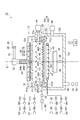
- FIG. 1 is a cross-sectional view schematically showing a film forming apparatus according to an embodiment.
- the processing container 12 is a substantially cylindrical container extending in the direction in which the axis Z extends (hereinafter referred to as “axis Z direction”), and defines a space S therein.
- the space S includes a plasma generation chamber S1 and a processing chamber S2 provided below the plasma generation chamber S1.
- the processing container 12 may include a first sidewall 12a, a second sidewall 12b, a bottom 12c, and an upper portion 12d. These members constituting the processing container 12 are connected to the ground potential.
- the first side wall 12a has a substantially cylindrical shape extending in the axis Z direction, and defines a plasma generation chamber S1.
- Gas lines P11 and P12 are formed on the first side wall 12a.
- the gas line P11 extends from the outer surface of the first side wall 12a and is connected to the gas line P12.
- the gas line P12 extends substantially annularly about the axis Z in the first side wall 12a.
- a plurality of injection ports H1 for injecting gas into the plasma generation chamber S1 are connected to the gas line P12.
- a gas source G1 is connected to the gas line P11 through a valve V11, a mass flow controller M1, and a valve V12.
- the gas source G1 is a rare gas source, and in one embodiment, an Ar gas source.
- the gas source G1, the valve V11, the mass flow controller M1, the valve V12, the gas lines P11 and P12, and the injection port H1 constitute a first gas supply system according to an embodiment.
- the first gas supply system controls the flow rate of the rare gas from the gas source G1 in the mass flow controller M1, and supplies the flow-controlled rare gas to the plasma generation chamber S1.
- a gas source G3 may be connected to the gas line P11 via a valve V31, a mass flow controller M3, and a valve V32.
- the gas source G3 is a gas source of hydrogen gas (H 2 gas).
- the flow rate of hydrogen gas from the gas source G3 is controlled by the mass flow controller M3, and the hydrogen gas whose flow rate is controlled is supplied to the plasma generation chamber S1.
- the gas source G3, the valve V31, the mass flow controller M3, and the valve V32 together with the gas source G1, the valve V11, the mass flow controller M1, the valve V12, the gas lines P11 and P12, and the injection port H1 described above,
- a first gas supply system may be configured.
- an upper portion 12d is provided at the upper end of the first side wall 12a.
- An opening is provided in the upper part 12d, and an antenna 14 is provided in the opening.
- a dielectric window 16 is provided immediately below the antenna 14 so as to seal the plasma generation chamber S1.
- the antenna 14 supplies microwaves to the plasma generation chamber S1 through the dielectric window 16.
- the antenna 14 is a radial line slot antenna.
- the antenna 14 includes a dielectric plate 18 and a slot plate 20.
- the dielectric plate 18 shortens the wavelength of the microwave and has a substantially disk shape.
- the dielectric plate 18 is made of, for example, quartz or alumina.
- the dielectric plate 18 is sandwiched between the slot plate 20 and the metal lower surface of the cooling jacket 22.
- the antenna 14 can thus be constituted by the dielectric plate 18, the slot plate 20, and the lower surface of the cooling jacket 22.
- the slot plate 20 is a substantially disk-shaped metal plate in which a plurality of slot pairs are formed.
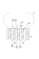
- FIG. 2 is a plan view showing an example of the slot plate.
- a plurality of slot pairs 20 a are formed in the slot plate 20.
- the plurality of slot pairs 20a are provided at predetermined intervals in the radial direction, and are arranged at predetermined intervals in the circumferential direction.
- Each of the plurality of slot pairs 20a includes two slot holes 20b and 20c.
- the slot hole 20b and the slot hole 20c extend in a direction intersecting or orthogonal to each other.
- the film forming apparatus 10 may further include a coaxial waveguide 24, a microwave generator 26, a tuner 28, a waveguide 30, and a mode converter 32.
- the microwave generator 26 generates a microwave having a frequency of 2.45 GHz, for example.
- the microwave generator 26 is connected to the upper portion of the coaxial waveguide 24 via a tuner 28, a waveguide 30, and a mode converter 32.
- the coaxial waveguide 24 extends along the axis Z that is the central axis thereof.
- the coaxial waveguide 24 includes an outer conductor 24a and an inner conductor 24b.
- the outer conductor 24a has a cylindrical shape extending in the center of the axis Z.
- the lower end of the outer conductor 24a can be electrically connected to the top of the cooling jacket 22 having a conductive surface.
- the inner conductor 24b is provided inside the outer conductor 24a.
- the inner conductor 24b has a substantially cylindrical shape extending along the axis Z.
- the microwave generated by the microwave generator 26 is propagated to the dielectric plate 18 through the coaxial waveguide 24, and applied to the dielectric window 16 from the slot hole of the slot plate 20. It is done.
- the dielectric window 16 has a substantially disk shape, and is made of, for example, quartz or alumina.
- the dielectric window 16 is provided immediately below the slot plate 20.
- the dielectric window 16 transmits the microwave received from the antenna 14 and introduces the microwave into the plasma generation chamber S1. As a result, an electric field is generated immediately below the dielectric window 16, and a rare gas plasma is generated in the plasma generation chamber S1. Further, when hydrogen gas is supplied to the plasma generation chamber S1 together with the rare gas, plasma of hydrogen gas is also generated.
- the film forming apparatus 10 further includes a mounting table 36 in the processing chamber S2.
- the mounting table 36 can support the substrate W to be processed on the upper surface thereof.
- the mounting table 36 is supported by a support body 38 extending in the axis Z direction from the bottom 12 c of the processing container 12.
- the mounting table 36 may include a suction holding mechanism such as an electrostatic chuck, and a temperature control mechanism such as a refrigerant flow path connected to the chiller unit and a heater.
- a pipe P21 extending annularly around the axis Z is provided above the mounting table 36.
- a plurality of injection ports H2 for injecting gas into the processing chamber S2 are formed.
- a gas source G2 is connected to the pipe P22 via a valve V21, a mass flow controller M2, and a valve V22.
- the gas source G2 is a gas source of a precursor gas, and in one embodiment, supplies a 1,3-dimethoxytetramethyldisoroxane (DMOTMDS) gas.
- DMOTMDS 1,3-dimethoxytetramethyldisoroxane
- the gas source G2, the valve V21, the mass flow controller M2, the valve V22, the pipes P21 and P12, and the injection port H2 constitute a second gas supply system according to an embodiment.
- the second gas supply system controls the flow rate of the precursor gas from the gas source G2 in the mass flow controller M2, and supplies the precursor gas whose flow rate is controlled to the processing chamber S2.
- the precursor gas supplied to the processing chamber S2 by the second gas supply system may be any gas having SiO in the gas molecule structure and having a methyl group (MTMOS, Di-iso-propyl-dimethylsilane, Isobutyl- dimethyl-methoxysilane, etc.), general gas having a member ring structure in the gas molecule structure (such as dimethyloxysilanecyclohexane, dimethyl-siloxanecyclohexane, 5-Slaspiro [4,4] nonane), benzene ring and 5-membered ring in the gas molecule structure It is also possible to use general gases having a structure that is easily broken by plasma (such as Dicclovalent-dimethylsilane).
- MTMOS Di-iso-propyl-dimethylsilane, Isobutyl- dimethyl-methoxysilane, etc.
- general gas having a member ring structure in the gas molecule structure such as dimethyloxysilane
- a gas source G4 may be connected to the gas line P22 via a valve V41, a mass flow controller M4, and a valve V42.
- the gas source G4 is a toluene gas source.
- the flow rate of toluene gas from the gas source G4 is controlled by the mass flow controller M4, and the toluene gas whose flow rate is controlled is supplied to the processing chamber S2.
- the gas source G4, the valve V41, the mass flow controller M4, and the valve V42 are the gas source G2, the valve V21, the mass flow controller M2, the valve V22, the gas lines P21 and P22, and the injection port H2.
- a second gas supply system according to an embodiment may be configured.
- a shielding unit 40 is provided between the plasma generation chamber S1 and the processing chamber S2.
- the shielding part 40 is a substantially disk-shaped member, and the shielding part 40 is formed with a plurality of openings 40h that allow the plasma generation chamber S1 and the processing chamber S2 to communicate with each other.
- the shielding part 40 is supported by the 1st side wall 12a, for example. In one embodiment, the shielding part 40 is sandwiched between the insulating member 60 and the insulating member 62, and is supported by the first side wall 12 a via these insulating members 60 and 62. Therefore, in one embodiment, the shielding part 40 is electrically separated from the first side wall 12a.
- a bias power source 42 for supplying bias power to the shielding unit 40 may be connected to the shielding unit 40.
- the bias power source 42 may be a power source that generates high-frequency bias power. In this embodiment, the bias power source 42 supplies high-frequency bias power to the shielding unit 40 in order to draw ions generated in the plasma generation chamber S ⁇ b> 1 into the shielding unit 40.
- a matching unit 43 having a matching circuit for matching the output impedance of the bias power source 42 and the load side, that is, the impedance on the shielding unit 40 side, is provided between the bias power source 42 and the shielding unit 40.
- the bias power source 42 may be a DC power source, and DC bias power may be applied to the shielding unit 40.
- the shielding unit 40 has a shielding property against ultraviolet rays generated in the plasma generation chamber S1. That is, the shielding unit 40 can be made of a material that does not transmit ultraviolet rays. In one embodiment, the shielding unit 40 donates electrons to the ions when the ions generated in the plasma generation chamber S1 are reflected by the inner wall surface defining the opening 40h and pass through the opening 40h. . Thereby, the shielding part 40 neutralizes ion and discharge
- the shield 40 has a thickness of 10 mm and a diameter of 40 cm.
- the diameter of the shielding part 40 is defined by the diameter of the surface in contact with the plasma generation chamber S1.
- opening 40h of shielding part 40 has a diameter of 1 mm.
- the aperture ratio of the shielding part 40 is 10%.
- the opening ratio of the shielding part 40 is defined by the ratio of the area occupied by the opening 40h to the area of the surface in contact with the plasma generation chamber S1.
- the aperture ratio may be in the range of 5% to 10%.
- the film forming apparatus 10 can form a film on the substrate W to be processed of 8 inches or more by including the shielding unit 40 having a diameter of 40 cm or more.
- the shielding part 40 having such a large diameter has a large conductance.
- D is the diameter of the shielding part 40
- B is an aperture ratio.
- the pressure in the plasma generation chamber S1 is set to 4 times or more of the pressure in the processing chamber S2, that is, the pressure ratio is set to 4 or more, and the diffusivity is set to 0.01 or less.
- the diffusivity is defined as an increase in Pascal unit of the pressure in the plasma generation chamber S1 when the flow rate of the precursor gas supplied to the processing chamber S2 increases by 1 sccm.
- This diffusivity is obtained by supplying a rare gas to the plasma generation chamber S1, increasing the flow rate of the precursor gas supplied to the processing chamber S2, and graphing the relationship between the flow rate of the precursor gas and the amount of pressure increase in the plasma generation chamber. And can be obtained from the slope of the graph.
- the diffusivity partially depends on the pressure ratio, but also depends on the conductance of the shielding unit 40, the flow rate of the rare gas, the flow rate of the precursor gas, and the like.
- the film forming apparatus 10 includes a pressure gauge 44 that measures the pressure in the plasma generation chamber S1 and a pressure gauge 46 that measures the pressure in the processing chamber S2.
- a pressure regulator 50 and a decompression pump 52 are connected to the exhaust pipe 48 connected to the processing chamber S2 at the bottom 12c.
- the pressure regulator 50 and the decompression pump 52 constitute an exhaust device.
- the flow rate of the rare gas is adjusted by the mass flow controller M1
- the flow rate of the precursor gas is adjusted by the mass flow controller M2
- the pressure adjustment is further performed.
- the exhaust volume can be adjusted by the vessel 50. Thereby, the film-forming apparatus 10 can set said pressure ratio and diffusivity.
- the film forming apparatus 10 further includes a control unit Cnt.
- the control unit Cnt may be a controller such as a programmable computer device.
- the control unit Cnt can control each unit of the film forming apparatus 10 according to a program based on the recipe. For example, the control unit Cnt can send a control signal to the valves V11 and V12 to control the supply and stop of the rare gas, and send a control signal to the mass flow controller M1 to control the flow rate of the rare gas. can do.
- the control unit Cnt can send control signals to the valves V31 and V32 to control supply and stop of supply of hydrogen gas, and send control signals to the mass flow controller M3 to control the flow rate of hydrogen gas. can do.
- control unit Cnt can send control signals to the valves V21 and V22 to control the supply and stop of the precursor gas, and send a control signal to the mass flow controller M2 to flow the precursor gas. Can be controlled.
- the control unit Cnt can send a control signal to the valves V41 and V42 to control supply and stop of toluene gas, and send a control signal to the mass flow controller M4 to control the flow rate of toluene gas. can do.
- control unit Cnt can send a control signal to the pressure regulator 50 to control the exhaust amount.
- control unit Cnt sends a control signal to the microwave generator 26 to control the power of the microwave, and sends a control signal to the bias power source 42 to supply and supply bias power to the shielding unit 40. It is possible to stop and further control the power of the bias power (for example, RF power).
- bias power for example, RF power
- FIG. 3 shows a plasma PL of argon gas, which is a rare gas.
- argon ions are indicated by “Ar + ” surrounded by a circle
- electrons are indicated by “e” surrounded by a circle
- photons are indicated by “P” surrounded by a circle.
- Electrons in the plasma PL are reflected by the shield 40 and returned to the plasma generation chamber S1. Photons are shielded by the shield 40.
- argon ions receive electrons from the shielding part 40 by contacting the inner wall surface defining the opening 40 h in the middle of the opening 40 h of the shielding part 40. Thereby, the argon ions are neutralized and then released as neutral particles into the processing chamber S2.
- neutral particles of argon are indicated by “Ar” surrounded by a circle.
- the precursor gas is supplied to the processing chamber S2.
- the pressure ratio is set to 4 or more and the diffusivity is set to 0.01 or less so that the diffusion of the precursor gas from the processing chamber S2 to the plasma generation chamber S1 is reduced. . Therefore, in this method, the diffusion amount of the precursor gas into the plasma generation chamber S1 is reduced, and the phenomenon that the precursor gas is excessively dissociated can be suppressed.
- the processing chamber S2 neutral particles of argon are irradiated to the DMOTMDS gas that is the precursor gas.
- rare gas plasma is excited in the plasma generation chamber S1 by microwaves, in one embodiment, by microwaves supplied from a radial line slot antenna.
- the microwave can generate high-density and low-temperature plasma even in a wide pressure range from the low pressure region to the high pressure region. Therefore, the particles passing through the shielding part have energy capable of suppressing excessive dissociation of the precursor gas.
- a film having a high density can be obtained.
- the film formation using the film forming apparatus 10 can also be performed by controlling the temperature of the mounting table 36 and setting the temperature of the substrate to be processed W to 100 ° C. or lower, for example, ⁇ 50 ° C. . Therefore, the film can be formed while suppressing damage due to the temperature of the device included in the substrate W to be processed.
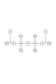
- the precursor gas is excessively dissociated due to the production method, and as a result, the cage structure shown in FIG. A film is formed. That is, conventionally, the dielectric constant is reduced by making the film mainly composed of silicon oxide into a porous film.
- the method for forming a low dielectric constant film according to an embodiment it is possible to realize a high density of the film as well as a low dielectric constant of the film.
- the process conditions may be adjusted so that the cage structure shown in FIG. 6A and the network structure shown in FIG. 6B are included in a part of the film.
- bias power may be supplied to the shielding unit 40.
- This bias power may be a high frequency bias power or a DC bias power.
- the relative dielectric constant of the low dielectric constant film is further reduced.
- the reason why the relative permittivity is further reduced by this method is estimated as follows. That is, the particles passing through the shielding unit 40 are accelerated by the bias power applied to the shielding unit 40.
- DMOTMDS is irradiated with particles accelerated by bias power, the polymerization of molecules derived from DMOTMDS is promoted, resulting in an increase in the chain length of the polymer in the low dielectric constant film, further increasing the orientation of the polymer. descend. Thereby, it is estimated that the relative dielectric constant of the low dielectric constant film is further reduced.
- bias power is supplied to the shielding unit 40, and hydrogen gas may be supplied to the plasma generation chamber S1 in addition to the rare gas.
- hydrogen gas may be supplied to the plasma generation chamber S1 in addition to the rare gas.
- toluene gas may be supplied to the processing chamber S2 together with the precursor gas.
- the side chain of the precursor gas is replaced with a phenyl group.
- the precursor gas is DMOTMDS
- a methyl group bonded to Si of MOTMDS is replaced with a phenyl group.
- the film forming apparatus 10 and the method for forming the low dielectric constant film capable of using the film forming apparatus 10 have been described.
- the relative dielectric constant is less than 2.7
- a SiCO film having a refractive index greater than 1.5 can be manufactured.
- the SiCO film is made of a polymer containing Si atoms, O atoms, C atoms, and H atoms.
- the SiCO film may have a structure in which a straight chain structure includes a siloxane bond, and a methyl group is substantially bonded to an Si atom constituting the siloxane bond.
- a SiCO film having a relative dielectric constant of 2.3 or less by applying a bias power to the shielding unit 40.
- the SiCO film in the spectrum of the signal obtained was analyzed by Fourier transform infrared spectroscopy, wavenumber 1010 cm -1 signal seen in the vicinity of the signal seen in the vicinity of wave number 1050 cm -1, wave number 1075 cm -1 signal seen in the vicinity of the signal seen in the vicinity of several 1108Cm -1, and the sum of the signal area of the wave number 1140 cm -1 signal seen in the vicinity is taken as 100%, observed in the vicinity of wavenumber 1108cm -1
- the signal area ratio is 25% or more.
- the signal area of these wavenumber signals is obtained by performing Gaussian fitting on the spectrum near the target wavenumber and obtaining the area of the fitted Gaussian signal.
- Wave number 1010 cm -1 signal seen in the vicinity of wave number 1050 cm -1 signal seen in the vicinity of wave number 1075 cm -1 signal seen in the vicinity of wavenumber 1108cm -1 signal seen in the vicinity, and the wave number 1140 cm -1 signal seen in the vicinity Are signals indicating siloxane bonds having different bond angles.
- a signal seen in the vicinity of a wave number of 1108 cm ⁇ 1 is a signal indicating a siloxane bond having a bond angle of about 150 °.
- the coupling angle is, for example, in the range of about 147 ° to 154 °.
- Such a siloxane bond contributes to increasing the symmetry of the linear structure in the SiCO film and lowering the relative dielectric constant. Therefore, when the area ratio of signals that are observed in the vicinity of a wave number of 1108 cm ⁇ 1 among signals indicating siloxane bonds is 25% or more, the SiCO film is a SiCO film having a low relative dielectric constant.
- a SiCO film having a relative dielectric constant of 2.15 or less by applying a bias power to the shielding unit 40 and supplying a hydrogen gas together with a rare gas to the plasma generation chamber S1. It becomes.
- the area ratio of signals found in the vicinity of wave number 1108 cm ⁇ 1 is 40% or more with respect to the total sum of the signal areas, and the full width at half maximum of the signal seen in the vicinity of wave number 1108 cm ⁇ 1 is 35 or less.
- the full width at half maximum of the signal is obtained by performing Gaussian fitting on the spectrum near the wave number of interest and obtaining the full width at half maximum of the fitted Gaussian signal.
- more siloxane bonds increase the symmetry of the linear structure. Therefore, the SiCO film becomes a SiCO film having a lower relative dielectric constant.
- the SiCO films of the various embodiments described above have a low relative dielectric constant, a high refractive index, that is, a high density, and excellent moisture resistance. Therefore, the SiCO film can be suitably used as a cap film and / or an interlayer insulating film in a damascene wiring structure.
- FIG. 7 is a diagram illustrating a semiconductor device having a damascene wiring structure.
- a semiconductor device 100 shown in FIG. 7 includes elements such as MOS transistors 102 and 104 formed on a substrate Sub. Further, the semiconductor device 100 includes a damascene wiring structure DW that is electrically connected to these elements via contacts 106.
- the damascene wiring structure DW has a structure in which a cap layer 110, an interlayer insulating film 112, an etching stopper layer 114, and an interlayer insulating film 116 are sequentially stacked.
- a trench 120 is provided in the interlayer insulating film 116, and a wiring formed of a metal material such as copper is provided in the trench 120.
- a via 122 is formed in the interlayer insulating film 112 to connect the wiring formed in the upper interlayer insulating film 116 and the wiring formed in the lower interlayer insulating film 116 to each other. Is embedded with a metal material such as copper.
- the cap layer 110 is provided on the upper surface of the interlayer insulating film 116.
- the cap layer 110 is required to have a low relative dielectric constant and moisture resistance in order to reduce the capacitance between wirings.
- a SiCO film having a relative dielectric constant smaller than 2.7 can be obtained.
- this SiCO film has a refractive index smaller than 1.5, that is, a high density, it has excellent moisture resistance. Therefore, this SiCO film is suitable for use as the cap layer 110.
- This SiCO film may be used as the interlayer insulating films 112 and 116.
- the precursor gas supplied to the processing chamber S2 may be OMCTS (octamethylcyclotetrasiloxane: [(CH 3 ) 2 SiO] 4 ).
- OMCTS octamethylcyclotetrasiloxane: [(CH 3 ) 2 SiO] 4
- an additive gas composed of at least one of H 2 O, CH 3 OH, C 2 H 5 OH, TMAH (tetramethylammonium hydroxide), and NH 3 is used instead of hydrogen gas. It may be supplied. Note that the additive gas may be supplied to the processing chamber S2.
- a low dielectric constant film was formed on a target substrate W having a diameter of 200 mm using the film forming apparatus 10 under the conditions of Experimental Examples 1 to 4 and Comparative Examples 1 to 20 shown in Table 1 below.
- the temperature of the substrate to be processed W was set to ⁇ 50 ° C.
- a low dielectric constant film was formed under the conditions of Comparative Examples 21 to 29 shown in Table 1 using a film forming apparatus different from the film forming apparatus 10 in that an inductively coupled plasma source was used.
- a shielding part made of graphite having a diameter of 40 cm, a thickness of 10 mm, and an opening having a diameter of 1 mm with an aperture ratio of 10% is used as the shielding part 40. It was.
- CW in the MODE column indicates that radio frequency (RF) power is continuously applied to the coil of the inductively coupled plasma source.
- TM A / B in the MODE column indicates that the RF power applied to the coil of the inductively coupled plasma source is time-modulated, and the cycle in which the RF power is stopped for A second and then applied to the coil for B second. Is repeated.
- FIG. 8 shows the relationship between the relative dielectric constant k and the refractive index RI of the low dielectric constant films obtained in each experimental example and comparative example.
- the horizontal axis represents the refractive index RI
- the vertical specific axis represents the relative dielectric constant k.
- FIG. 8 shows, as a comparative example 30, a refractive index RI and a relative dielectric constant k of a film in which a porous film is used to reduce the dielectric constant.
- the low dielectric constant film of Experimental Example 1 has a higher carbon concentration than the low dielectric constant films of Comparative Examples 3, 15 and 30.
- methyl groups are present from DMOTMDS. It was confirmed that it was not separated excessively.
- the C / Si concentration ratio and the O / Si concentration ratio of the low dielectric constant film shown in Table 2 it is estimated that the film mainly including the linear structure shown in FIG. Is done.
- the density of the low dielectric constant film of Experimental Example 1 is considerably larger than the density of the low dielectric constant films of Comparative Examples 3, 15, and 30.
- FIG. 9 shows the relationship between the pressure ratio and the diffusivity obtained in this experiment.
- the diffusivity is 0.01 or less.
- the diffusivity may be 0.01 or less.
- the diffusivity is set to 0.01 or less and the pressure is set. It was confirmed that it was necessary to set the ratio to 4 or more.
- a low dielectric constant film was formed on the target substrate W having a diameter of 200 mm under the conditions shown in Table 3 below.
- the temperature of the substrate to be processed W was set to ⁇ 50 ° C. More specifically, in Experimental Example 5, only the Ar gas was supplied to the plasma generation chamber S ⁇ b> 1 and the high-frequency bias power was supplied to the shielding unit 40 using the film forming apparatus 10.
- Ar gas and H 2 gas were supplied to the plasma generation chamber S 1, and high-frequency bias power was supplied to the shielding unit 40.
- Comparative Example 31 the film forming apparatus 10 was used, Ar gas and O 2 gas were supplied to the plasma generation chamber S1, and high frequency bias power was supplied to the shielding unit 40.
- Comparative Example 32 the film forming apparatus 10 was used, Ar gas and MTMOS (methyltrimethylsilane) gas were supplied to the plasma generation chamber S1, and high frequency bias power was supplied to the shielding unit 40.
- the shielding part 40 a shielding part made of graphite having a diameter of 40 cm, a thickness of 10 mm, and an opening having a diameter of 1 mm with an aperture ratio of 10%. was used.
- the low dielectric constant films prepared in Experimental Examples 1, 5, and 6 are heated in vacuum from room temperature to 400 ° C. at a heating rate of 10 ° C. per minute. The rate of decrease was measured. As a result of this measurement, the film thickness reduction rates of the low dielectric constant films of Experimental Examples 1, 5, and 6 were 23%, 32%, and 5%, respectively. From this, by supplying bias power to the shielding part 40 and supplying Ar gas and H 2 gas to the plasma generation chamber, the heat resistance of the low dielectric constant film is improved, that is, the polymerizability is increased. It was confirmed.
- toluene gas was supplied to the processing chamber S2 at a flow rate of 30 sccm, and a low dielectric constant film was formed on 10 substrates to be processed W having a diameter of 200 mm.
- the temperature of the substrate to be processed W was set to ⁇ 50 ° C.
- Other conditions in Experimental Example 7 are the same as in Experimental Example 5.
- the average value of the relative dielectric constant and the average value of the polarizability of the low dielectric constant film formed on the ten substrates to be processed W by the processing of Experimental Example 7 were obtained.
- the average value of the relative dielectric constant and the average value of the polarizability of the low dielectric constant film formed on 10 substrates to be processed W by the treatment of Experimental Example 7 were 2.24 and 0.2, respectively.
- the polarizabilities of the low dielectric constant films formed by the processes of Experimental Examples 1 to 4 and Comparative Examples 1 to 29 were also calculated.
- the polarizability can be calculated by the square of (relative permittivity-refractive index).
- the polarizabilities of the low dielectric constant films formed by the treatments of Experimental Examples 1 to 4 and Comparative Examples 1 to 29 were calculated.
- the low dielectric constant film was a low dielectric constant film formed by the treatment of Experimental Example 4, and the polarizability was about 1.0. From this, it was confirmed that the relative dielectric constant and the polarizability of the low dielectric constant film can be further reduced by supplying toluene gas together with the precursor gas to the processing chamber S2.
- the low dielectric constant films that is, SiCO films prepared in Experimental Examples 4 to 6, were analyzed by Fourier transform infrared spectroscopy. Then, for each of the experimental examples, the signal from the spectrum obtained by Fourier transform infrared spectroscopy, signal seen in the vicinity of wave number 1010 cm -1, the signal observed in the vicinity of wave number 1050 cm -1, it is found in the vicinity of wave number 1075 cm -1, wave number 1108Cm -1 signal seen in the vicinity, and determine the respective signal area of the wave number 1140 cm -1 signal seen in the vicinity, when the sum of these signals area to 100%, of the signal seen in the vicinity of wavenumber 1108cm -1 The area ratio (%) was determined. The signal area was obtained by performing Gaussian fitting on the spectrum in the vicinity of the target wavenumber and obtaining the area of the fitted Gaussian signal.
- the full width at half maximum of the signal found in the vicinity of the wave number of 1108 cm ⁇ 1 was obtained from the spectrum obtained by Fourier transform infrared spectroscopy.
- the full width at half maximum of the signal was obtained by performing Gaussian fitting on the spectrum in the vicinity of the wave number of interest and obtaining the full width at half maximum of the fitted Gaussian signal.
- the area ratio of signals found in the vicinity of the wave number of 1108 cm ⁇ 1 is about 25% or more, and many siloxane bonds that enhance the symmetry of the linear structure are contained. It was confirmed that In addition, in the SiCO film of Experimental Example 6, the area ratio of the signal seen in the vicinity of the wave number of 1108 cm ⁇ 1 was about 40% or more, and it was confirmed that more siloxane bonds that improve the symmetry of the linear structure were included. .
- the spectrum obtained by applying Fourier transform infrared spectroscopy to the SiCO film of Experimental Example 6 is shown in FIG. As shown in FIG.
- the SiCO film of Experimental Example 6 contains more siloxane bonds that improve the symmetry of the linear structure and have a small bond angle variation.
- gas source precursor gas
- H2 injection port
- M2 mass flow controller
- Cnt control unit
- 100 semiconductor device, DW ... damascene wiring structure, 102 ... transistor, 110 ... cap layer, 112 ... interlayer insulating film, 114 Etch stop layer, 116 ... interlayer insulating film, 120 ... trench, 122 ... via.
Landscapes
- Chemical & Material Sciences (AREA)
- Engineering & Computer Science (AREA)
- Physics & Mathematics (AREA)
- Organic Chemistry (AREA)
- Chemical Kinetics & Catalysis (AREA)
- General Chemical & Material Sciences (AREA)
- Materials Engineering (AREA)
- Mechanical Engineering (AREA)
- Metallurgy (AREA)
- Plasma & Fusion (AREA)
- Power Engineering (AREA)
- Analytical Chemistry (AREA)
- Microelectronics & Electronic Packaging (AREA)
- Condensed Matter Physics & Semiconductors (AREA)
- General Physics & Mathematics (AREA)
- Computer Hardware Design (AREA)
- Manufacturing & Machinery (AREA)
- Inorganic Chemistry (AREA)
- Spectroscopy & Molecular Physics (AREA)
- Chemical Vapour Deposition (AREA)
- Internal Circuitry In Semiconductor Integrated Circuit Devices (AREA)
- Formation Of Insulating Films (AREA)
- Plasma Technology (AREA)
Priority Applications (2)
| Application Number | Priority Date | Filing Date | Title |
|---|---|---|---|
| KR1020157003666A KR102030223B1 (ko) | 2012-08-23 | 2013-06-18 | 성막 장치, 저유전율막을 형성하는 방법, SiCO막 및 다마신 배선 구조 |
| US14/422,455 US20150214015A1 (en) | 2012-08-23 | 2013-06-18 | FILM FORMING APPARATUS, METHOD OF FORMING LOW-PERMITTIVITY FILM, SiCO FILM, AND DAMASCENE INTERCONNECT STRUCTURE |
Applications Claiming Priority (6)
| Application Number | Priority Date | Filing Date | Title |
|---|---|---|---|
| JP2012-184298 | 2012-08-23 | ||
| JP2012184298 | 2012-08-23 | ||
| JP2012252467 | 2012-11-16 | ||
| JP2012-252467 | 2012-11-16 | ||
| JP2013-096456 | 2013-05-01 | ||
| JP2013096456A JP6172660B2 (ja) | 2012-08-23 | 2013-05-01 | 成膜装置、及び、低誘電率膜を形成する方法 |
Publications (1)
| Publication Number | Publication Date |
|---|---|
| WO2014030414A1 true WO2014030414A1 (ja) | 2014-02-27 |
Family
ID=50149732
Family Applications (1)
| Application Number | Title | Priority Date | Filing Date |
|---|---|---|---|
| PCT/JP2013/066731 Ceased WO2014030414A1 (ja) | 2012-08-23 | 2013-06-18 | 成膜装置、低誘電率膜を形成する方法、SiCO膜、及びダマシン配線構造 |
Country Status (5)
| Country | Link |
|---|---|
| US (1) | US20150214015A1 (enExample) |
| JP (1) | JP6172660B2 (enExample) |
| KR (1) | KR102030223B1 (enExample) |
| TW (1) | TW201419414A (enExample) |
| WO (1) | WO2014030414A1 (enExample) |
Cited By (2)
| Publication number | Priority date | Publication date | Assignee | Title |
|---|---|---|---|---|
| WO2015136743A1 (ja) * | 2014-03-13 | 2015-09-17 | 東京エレクトロン株式会社 | 低誘電率膜 |
| CN106601580A (zh) * | 2015-10-19 | 2017-04-26 | 北京北方微电子基地设备工艺研究中心有限责任公司 | 进气机构及反应腔室 |
Families Citing this family (16)
| Publication number | Priority date | Publication date | Assignee | Title |
|---|---|---|---|---|
| US10325773B2 (en) | 2012-06-12 | 2019-06-18 | Novellus Systems, Inc. | Conformal deposition of silicon carbide films |
| US9234276B2 (en) | 2013-05-31 | 2016-01-12 | Novellus Systems, Inc. | Method to obtain SiC class of films of desired composition and film properties |
| US12334332B2 (en) | 2012-06-12 | 2025-06-17 | Lam Research Corporation | Remote plasma based deposition of silicon carbide films using silicon-containing and carbon-containing precursors |
| US20180347035A1 (en) | 2012-06-12 | 2018-12-06 | Lam Research Corporation | Conformal deposition of silicon carbide films using heterogeneous precursor interaction |
| US10832904B2 (en) | 2012-06-12 | 2020-11-10 | Lam Research Corporation | Remote plasma based deposition of oxygen doped silicon carbide films |
| US20150118416A1 (en) * | 2013-10-31 | 2015-04-30 | Semes Co., Ltd. | Substrate treating apparatus and method |
| US20160314964A1 (en) | 2015-04-21 | 2016-10-27 | Lam Research Corporation | Gap fill using carbon-based films |
| JP2016219450A (ja) * | 2015-05-14 | 2016-12-22 | 株式会社アルバック | 基板処理装置 |
| US10840087B2 (en) | 2018-07-20 | 2020-11-17 | Lam Research Corporation | Remote plasma based deposition of boron nitride, boron carbide, and boron carbonitride films |
| KR102841276B1 (ko) * | 2018-07-24 | 2025-07-31 | 램 리써치 코포레이션 | 실리콘-함유 전구체 및 탄소-함유 전구체를 사용한 탄화 실리콘 막들의 리모트 플라즈마 기반 증착 |
| JP2020033625A (ja) * | 2018-08-31 | 2020-03-05 | 東京エレクトロン株式会社 | 成膜装置及び成膜方法 |
| WO2020081367A1 (en) | 2018-10-19 | 2020-04-23 | Lam Research Corporation | Doped or undoped silicon carbide deposition and remote hydrogen plasma exposure for gapfill |
| KR102617960B1 (ko) | 2019-08-12 | 2023-12-26 | 삼성전자주식회사 | 2-스텝 갭-필 공정을 이용하여 반도체 소자를 형성하는 방법 |
| CN112928008B (zh) * | 2019-12-06 | 2023-03-24 | 中微半导体设备(上海)股份有限公司 | 气体供应系统及其气体输送方法、等离子体处理装置 |
| US12442080B2 (en) * | 2023-11-16 | 2025-10-14 | Applied Materials, Inc. | Plasma showerhead assembly and method of reducing defects |
| US20250166973A1 (en) * | 2023-11-16 | 2025-05-22 | Applied Materials, Inc. | Plasma showerhead assembly and method of reducing defects |
Citations (6)
| Publication number | Priority date | Publication date | Assignee | Title |
|---|---|---|---|---|
| JP2005089823A (ja) * | 2003-09-17 | 2005-04-07 | Seiji Sagawa | 成膜装置および成膜方法 |
| JP2006074048A (ja) * | 2004-08-30 | 2006-03-16 | Samsung Corning Co Ltd | 二重有機シロキサン前駆体を用いた絶縁膜の製造方法 |
| JP2007266462A (ja) * | 2006-03-29 | 2007-10-11 | National Institute Of Advanced Industrial & Technology | シリカ薄膜及びその製造方法 |
| JP2008071894A (ja) * | 2006-09-13 | 2008-03-27 | Tokyo Electron Ltd | 成膜方法 |
| JP2009071163A (ja) * | 2007-09-14 | 2009-04-02 | Tokyo Electron Ltd | 半導体製造方法、半導体製造装置および表示装置 |
| JP2012144786A (ja) * | 2011-01-13 | 2012-08-02 | Semiconductor Technology Academic Research Center | 中性粒子照射型cvd装置 |
Family Cites Families (6)
| Publication number | Priority date | Publication date | Assignee | Title |
|---|---|---|---|---|
| US6635117B1 (en) * | 2000-04-26 | 2003-10-21 | Axcelis Technologies, Inc. | Actively-cooled distribution plate for reducing reactive gas temperature in a plasma processing system |
| JP4371543B2 (ja) * | 2000-06-29 | 2009-11-25 | 日本電気株式会社 | リモートプラズマcvd装置及び膜形成方法 |
| TW200537695A (en) * | 2004-03-19 | 2005-11-16 | Adv Lcd Tech Dev Ct Co Ltd | Insulating film forming method, insulating film forming apparatus, and plasma film forming apparatus |
| JP4633425B2 (ja) * | 2004-09-17 | 2011-02-16 | 東京エレクトロン株式会社 | プラズマ処理装置およびプラズマ処理方法 |
| WO2007136131A1 (ja) * | 2006-05-22 | 2007-11-29 | Kabushiki Kaisha Toyota Chuo Kenkyusho | 非晶質炭素膜、非晶質炭素膜の形成方法、非晶質炭素膜を備えた導電性部材および燃料電池用セパレータ |
| JP4743229B2 (ja) | 2008-05-29 | 2011-08-10 | 国立大学法人東北大学 | 中性粒子を用いた半導体装置の成膜方法 |
-
2013
- 2013-05-01 JP JP2013096456A patent/JP6172660B2/ja not_active Expired - Fee Related
- 2013-06-18 WO PCT/JP2013/066731 patent/WO2014030414A1/ja not_active Ceased
- 2013-06-18 US US14/422,455 patent/US20150214015A1/en not_active Abandoned
- 2013-06-18 KR KR1020157003666A patent/KR102030223B1/ko not_active Expired - Fee Related
- 2013-08-22 TW TW102130031A patent/TW201419414A/zh unknown
Patent Citations (6)
| Publication number | Priority date | Publication date | Assignee | Title |
|---|---|---|---|---|
| JP2005089823A (ja) * | 2003-09-17 | 2005-04-07 | Seiji Sagawa | 成膜装置および成膜方法 |
| JP2006074048A (ja) * | 2004-08-30 | 2006-03-16 | Samsung Corning Co Ltd | 二重有機シロキサン前駆体を用いた絶縁膜の製造方法 |
| JP2007266462A (ja) * | 2006-03-29 | 2007-10-11 | National Institute Of Advanced Industrial & Technology | シリカ薄膜及びその製造方法 |
| JP2008071894A (ja) * | 2006-09-13 | 2008-03-27 | Tokyo Electron Ltd | 成膜方法 |
| JP2009071163A (ja) * | 2007-09-14 | 2009-04-02 | Tokyo Electron Ltd | 半導体製造方法、半導体製造装置および表示装置 |
| JP2012144786A (ja) * | 2011-01-13 | 2012-08-02 | Semiconductor Technology Academic Research Center | 中性粒子照射型cvd装置 |
Non-Patent Citations (2)
| Title |
|---|
| KIM, S.-Y. ET AL.: "Characterization of ultra low-k SiOC(H) film deposited by plasma-enhanced chemical vapor deposition (PECVD)", TRANSACTIONS ON ELECTRICAL AND ELECTRONIC MATERIALS, vol. 13, no. 2, 25 April 2012 (2012-04-25), pages 69 - 72 * |
| R. NAVAMATHAVAN ET AL.: "Plasma enhanced chemical vapor deposition of low dielectric constant SiOC(-H) films using MTES/02 precursor", THIN SOLID FILMS, vol. 515, no. 12, 5 December 2006 (2006-12-05), pages 5040 - 5044 * |
Cited By (2)
| Publication number | Priority date | Publication date | Assignee | Title |
|---|---|---|---|---|
| WO2015136743A1 (ja) * | 2014-03-13 | 2015-09-17 | 東京エレクトロン株式会社 | 低誘電率膜 |
| CN106601580A (zh) * | 2015-10-19 | 2017-04-26 | 北京北方微电子基地设备工艺研究中心有限责任公司 | 进气机构及反应腔室 |
Also Published As
| Publication number | Publication date |
|---|---|
| KR102030223B1 (ko) | 2019-10-08 |
| JP6172660B2 (ja) | 2017-08-02 |
| KR20150046028A (ko) | 2015-04-29 |
| TW201419414A (zh) | 2014-05-16 |
| US20150214015A1 (en) | 2015-07-30 |
| JP2014116576A (ja) | 2014-06-26 |
Similar Documents
| Publication | Publication Date | Title |
|---|---|---|
| JP6172660B2 (ja) | 成膜装置、及び、低誘電率膜を形成する方法 | |
| WO2015108065A1 (ja) | 成膜方法及び熱処理装置 | |
| WO2012066779A1 (en) | Apparatus for plasma treatment and method for plasma treatment | |
| TW200416874A (en) | Plasma processing apparatus and method | |
| KR20090007773A (ko) | 성막 방법, 성막 장치 및 기억 매체, 및 반도체 장치 | |
| CN101356638A (zh) | 半导体装置和半导体装置的制造方法 | |
| JP2003168676A (ja) | 有機絶縁膜のエッチング方法 | |
| US20080311313A1 (en) | Film Forming Method and Film Forming Apparatus | |
| TWI510665B (zh) | 使用電漿反應製程來形成氟碳化物層的方法 | |
| KR100922448B1 (ko) | 플라즈마 성막방법 및 그 장치 | |
| WO2015184573A1 (zh) | 一种超低介电常数绝缘薄膜及其制备方法 | |
| US9472392B2 (en) | Step coverage dielectric | |
| KR101635120B1 (ko) | 절연막 재료, 이 절연막 재료를 이용한 성막 방법 및 절연막 | |
| JPH09134910A (ja) | プラズマ化学気相成長装置および半導体装置の製造方法 | |
| TWI587396B (zh) | Semiconductor device manufacturing method and semiconductor device | |
| JP5442871B2 (ja) | 半導体デバイスの製造方法および半導体デバイスの製造装置 | |
| JPH0969518A (ja) | シリコン化合物系絶縁膜の成膜方法 | |
| WO2015136743A1 (ja) | 低誘電率膜 | |
| JP2005123389A (ja) | プラズマ処理方法、プラズマ成膜方法、プラズマエッチング方法およびプラズマ処理装置 | |
| US20110223766A1 (en) | Method and apparatus for manufacturing semiconductor device | |
| Hori | Plasma Etching Technology for Low-k Porous SiOCH Films | |
| JP2015195282A (ja) | 成膜方法、半導体製造方法及び半導体装置 |
Legal Events
| Date | Code | Title | Description |
|---|---|---|---|
| 121 | Ep: the epo has been informed by wipo that ep was designated in this application |
Ref document number: 13830529 Country of ref document: EP Kind code of ref document: A1 |
|
| ENP | Entry into the national phase |
Ref document number: 20157003666 Country of ref document: KR Kind code of ref document: A |
|
| WWE | Wipo information: entry into national phase |
Ref document number: 14422455 Country of ref document: US |
|
| NENP | Non-entry into the national phase |
Ref country code: DE |
|
| 122 | Ep: pct application non-entry in european phase |
Ref document number: 13830529 Country of ref document: EP Kind code of ref document: A1 |