WO2014021245A1 - 光学フィルタ - Google Patents
光学フィルタ Download PDFInfo
- Publication number
- WO2014021245A1 WO2014021245A1 PCT/JP2013/070432 JP2013070432W WO2014021245A1 WO 2014021245 A1 WO2014021245 A1 WO 2014021245A1 JP 2013070432 W JP2013070432 W JP 2013070432W WO 2014021245 A1 WO2014021245 A1 WO 2014021245A1
- Authority
- WO
- WIPO (PCT)
- Prior art keywords
- light
- optical filter
- shielding film
- light shielding
- infrared
- Prior art date
- Legal status (The legal status is an assumption and is not a legal conclusion. Google has not performed a legal analysis and makes no representation as to the accuracy of the status listed.)
- Ceased
Links
Images







Classifications
-
- G—PHYSICS
- G02—OPTICS
- G02B—OPTICAL ELEMENTS, SYSTEMS OR APPARATUS
- G02B5/00—Optical elements other than lenses
- G02B5/20—Filters
- G02B5/208—Filters for use with infrared or ultraviolet radiation, e.g. for separating visible light from infrared and/or ultraviolet radiation
-
- G—PHYSICS
- G02—OPTICS
- G02B—OPTICAL ELEMENTS, SYSTEMS OR APPARATUS
- G02B5/00—Optical elements other than lenses
- G02B5/003—Light absorbing elements
-
- G—PHYSICS
- G02—OPTICS
- G02B—OPTICAL ELEMENTS, SYSTEMS OR APPARATUS
- G02B5/00—Optical elements other than lenses
- G02B5/005—Diaphragms
-
- G—PHYSICS
- G02—OPTICS
- G02B—OPTICAL ELEMENTS, SYSTEMS OR APPARATUS
- G02B5/00—Optical elements other than lenses
- G02B5/20—Filters
- G02B5/205—Neutral density filters
-
- G—PHYSICS
- G03—PHOTOGRAPHY; CINEMATOGRAPHY; ANALOGOUS TECHNIQUES USING WAVES OTHER THAN OPTICAL WAVES; ELECTROGRAPHY; HOLOGRAPHY
- G03B—APPARATUS OR ARRANGEMENTS FOR TAKING PHOTOGRAPHS OR FOR PROJECTING OR VIEWING THEM; APPARATUS OR ARRANGEMENTS EMPLOYING ANALOGOUS TECHNIQUES USING WAVES OTHER THAN OPTICAL WAVES; ACCESSORIES THEREFOR
- G03B11/00—Filters or other obturators specially adapted for photographic purposes
Definitions
- the present invention relates to an optical filter.
- a filter optical filter having a specific function is disposed between the imaging lens and the solid-state imaging device.
- a typical example is a filter (near-infrared cut filter) that blocks light in the near-infrared wavelength region in order to correct the spectral sensitivity of a solid-state image sensor to human visibility. It arrange
- the imaging device adjusts the amount of incoming light to prevent the imaging device from saturating the charge generated by light reception and preventing imaging, and the optical members such as lenses and sensors in the imaging device and the like.
- a shielding member called a diaphragm is disposed.
- a method for realizing downsizing of an imaging device for example, a method of integrally providing a black coating (light shielding film) that functions as a light shielding member on an optical filter is known (see, for example, Patent Document 1).
- This method eliminates the need for a space for disposing the diaphragm, and can reduce the size of the apparatus. In addition, the number of parts can be reduced and the assembly process can be simplified.
- An object of the present invention is to provide an optical filter that is integrally provided with a light-shielding film that is excellent in productivity and economy and that can suppress stray light that causes image quality degradation.
- An optical filter according to an aspect of the present invention is an optical filter used in an imaging device including an imaging element into which light from a subject or a light source is incident, and is disposed between the subject or the light source and the imaging element. And an optical filter body having transparency to the incident light, and a frame-shaped light shielding film integrally formed on at least one surface of the optical filter body. And / or the condition (2) is satisfied. (1) Concavities and convexities are formed on at least part of the inner peripheral surface of the frame-shaped light shielding film in plan view. (2) Thin portions are formed on at least part of the inner edge of the frame-shaped light shielding film.
- an optical filter that is integrally provided with a light-shielding film that is excellent in productivity and economy and that can suppress stray light that causes image quality degradation.
- FIG. It is a top view which shows the optical filter of one Embodiment of this invention. It is sectional drawing of the optical filter shown in FIG. It is sectional drawing for demonstrating the diffraction suppression effect by the optical filter shown in FIG. It is sectional drawing for demonstrating the diffraction suppression effect by the optical filter shown in FIG. It is a top view which expands and shows the principal part of the optical filter shown in FIG. It is a graph which shows the convex part height of the light shielding film measured in one Example of this invention. It is a graph which shows the formation space
- FIG. 14B is a copy of an enlarged photograph of the photograph taken in FIG. 14A.
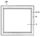
- FIG. 1 is a plan view schematically showing a near-infrared cut filter according to an embodiment of the present invention
- FIG. 2 is a sectional view thereof.
- the near-infrared cut filter 100 of the present embodiment is formed integrally with a near-infrared cut filter main body (hereinafter also simply referred to as “filter main body”) 10 and one main surface thereof. And a frame-shaped light shielding film (hereinafter also simply referred to as “light shielding film”) 20.
- filter main body a near-infrared cut filter main body
- light shielding film a frame-shaped light shielding film
- the filter body 10 is formed on the transparent base material 11 and one main surface of the transparent base material 11 and transmits light in the visible wavelength region but reflects light in the ultraviolet wavelength region and the infrared wavelength region.
- the light shielding film 20 is formed on the main surface of the filter main body 10 on the ultraviolet / infrared light reflecting film 12 side with a light shielding resin containing an inorganic or organic colorant such as carbon black or titanium black.
- a light shielding resin containing an inorganic or organic colorant such as carbon black or titanium black.
- the type of resin is not particularly limited, and any of a photocurable resin, a thermoplastic resin, and a thermosetting resin that is cured by irradiation with light in the ultraviolet wavelength region or the like can be used.
- “light shielding” refers to a property of blocking light transmission mainly by absorbing light.
- the light shielding film 20 made of such a light-shielding resin is light that enters the imaging element when the near-infrared cut filter 100 of the present embodiment is used in an imaging device that incorporates the imaging element as described later. It functions as a so-called aperture that adjusts the amount of light and cuts stray light.
- the frame-shaped light shielding film 20 has fine irregularities 22 formed on the inner peripheral surface thereof, and a thin portion 23 formed along the inner peripheral surface thereof.
- the unevenness 22 and the thin-walled portion 23 have a function of suppressing light from diffracting near the boundary between the light-shielding film 20 and the light-transmitting opening and stray light, which has been a conventional problem. . Note that only one of the unevenness 22 and the thin portion 23 may be provided.
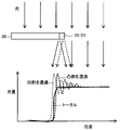
- FIG. 3 shows the transmission and transmission of light in the light shielding film 20A and its vicinity when light is incident on a near-infrared cut filter provided with a conventional light shielding film 20A in which the unevenness 22 and the thin portion 23 are not formed. It is the figure which showed notionally the quantity of light.
- 4 shows the light shielding film 20 and its vicinity when light is incident on the near-infrared cut filter 100 including the light shielding film 20 with the unevenness 22 and the thin portion 23 formed as shown in FIG. It is the figure which showed notion
- the light is diffracted at or near the inner edge of the light-shielding film 20A, and the intensity of the light is captured on the imaging surface of the imaging device that has received this light. Are distributed, and the quality of the peripheral portion of the image is deteriorated.
- the near-infrared cut filter of this embodiment as shown in FIG. 4, although the light is diffracted at the inner edge of the light shielding film 20, the diffracted light is multiplexed on the imaging surface of the image sensor. As a result, the light intensity becomes uniform. For this reason, an image in which stray light is hardly recognized is obtained.
- the arrow indicates the light ray direction of light incident in the cross-sectional direction of the light shielding film 20A or the light shielding film 20, but such a light shielding film is present on the imaging surface of the actual image sensor. Not only light that is incident perpendicular to the light 20 but also light that is incident obliquely or light that is reflected within the imaging device and deviates from a predetermined optical path is more complicated.
- the thin portion 23 absorbs or reflects light at the inner edge portion of the light shielding film 20 and suppresses the incidence of light on the image sensor. Moreover, the thin part 23 permeate
- the unevenness 22 and the thin-walled bamboo 23 formed on the light shielding film 20 satisfy at least one of the following conditions.
- the irregularities 22 are irregular.
- “irregularities are irregular” means that the irregularities are not regular or low in shape, size, pitch, arrangement method, etc. in plan view with respect to the light shielding film 20. (Hereinafter, when describing the unevenness 22, it means unevenness in plan view with respect to the light shielding film 20 unless otherwise specified). This is because if the irregularities are regular, points or lines where the diffracted light reinforces on the image sensor are generated, and the above-described diffraction suppressing effect may not be sufficiently obtained.
- the regularity is preferably as low as possible, more preferably no regularity.
- it is preferable that the height of the convex portion (or the depth of the concave portion) and the pitch, that is, the formation interval of adjacent convex portions (or concave portions) are irregular.
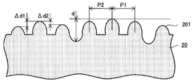
- At least two adjacent convex portions 201 have different heights, that is, a difference in height between the two adjacent convex portions 201.
- ⁇ d1 and ⁇ d2 are preferably positive. More preferably, ⁇ d1 and ⁇ d2 are positive and ⁇ d1 and ⁇ d2 are different, that is, ⁇ d1 ⁇ ⁇ d2. Further, even when the two adjacent convex portions 201 have the same height, that is, even when the height difference ⁇ d1, ⁇ d2 between the two adjacent convex portions 201 is zero, the pitches P1, P2 are different, that is, P1 ⁇ P2. If it is. More preferably, ⁇ d1 and ⁇ d2 are positive and P1 and P2 are P1 ⁇ P2, and ⁇ d1 and ⁇ d2 are positive, ⁇ d1 ⁇ ⁇ d2, and P1 ⁇ P2.
- the ratio P1 / P2 is more preferably 1.1 or more or 0.9 or less.
- the ratio P1 / P2 is more preferably 1.4 or more or 0.7 or less.
- ⁇ d1 and ⁇ d2 ⁇ d1 / d is preferably 0.1 or more, and more preferably 0.3 or more.
- / d is preferably 0.05 or more, and more preferably 0.1 or more.
- d is the maximum height of the convex portion 201, that is, the height from the deepest valley bottom of the unevenness 22 to the highest peak in FIG.
- 6A and 6B are graphs showing irregularities of the irregularities 22, and are actual measurement values of the irregularities 22 manufactured in Examples described later.
- 6A shows the height of the convex portion
- FIG. 6B shows the formation interval (pitch).
- the height (or depth of a recessed part) of the convex part 201 is more than the wavelength of the light which permeate
- the height of the convex portion 201 (or the depth of the concave portion) is too large, the diffracted light diffusing function is lowered, and a region in which the diffracted light is strengthened appears on the image sensor in a shape similar to the concave and convex portions.
- the diffraction suppressing effect is reduced.
- the height of the convex portion 201 (or the depth of the concave portion) is preferably about 0.5 ⁇ m or more and 10 ⁇ m or less for the wavelength of green light that maximizes the visibility in the application of the visible light imaging device.
- the light transmittance of the thin portion 23 is 0.5% or more. By setting the light transmittance to 0.5% or more, it is possible to sufficiently prevent the diffracted light from the inner edge of the light shielding film 20 from strengthening on the image sensor.
- the light transmittance is preferably 1% or more, and more preferably 3% or more.
- the average light transmittance of the thin portion 23 is preferably 80% or less, and more preferably 40% or less.
- the light transmittance of the portion other than the thin portion 23 of the light shielding film 20 is preferably less than 0.5%, more preferably 0.2% or less, and even more preferably 0.1% or less.
- the width w of the thin portion 23 having a light transmittance of 0.5% or more is 0.4 ⁇ m or more. By setting the width w to 0.4 ⁇ m or more, a greater diffraction suppressing effect can be obtained.
- the width w is more preferably 1 ⁇ m or more, and even more preferably 4 ⁇ m or more. On the other hand, if the width w exceeds 50 ⁇ m, stray light is likely to be transmitted. Therefore, the width w of the thin portion 23 is preferably 50 ⁇ m or less, and more preferably 20 ⁇ m or less.
- the thin portion 23 has an inclined surface 23a whose thickness gradually decreases toward the edge.
- the transmittance gradually increases toward the edge, the diffraction due to the transmittance changing stepwise is suppressed, and the diffraction light is sufficiently suppressed from strengthening on the imaging device. It is more preferable because it is possible.
- a mat surface-like uneven structure is formed on the surface of the light shielding film 20 (the surface opposite to the filter body 10, that is, the surface on the light incident side), or an antireflection film. It is preferable to provide an antireflection function for light.
- the mat surface-like concavo-convex structure has a surface roughness on the surface of the light-shielding film 20 on which the concavo-convex structure is formed, in accordance with JIS B0601 (1994). It is preferable that the arithmetic average roughness (Ra) measured by AFM) is 0.1 ⁇ m or more. A more preferable range of the arithmetic average roughness (Ra) is 0.15 to 10 ⁇ m, even more preferably 0.2 to 2 ⁇ m, and further preferably 0.2 to 0.5 ⁇ m.
- the average distance (S) of the local peaks measured by the ultra-deep shape measuring microscope in accordance with JIS B0601 (1994) is 1 to 100 ⁇ m, and further in accordance with JIS B0601 (1994).
- the maximum height (Ry) to be measured is preferably 2 ⁇ m or more.
- a more preferable range of the average distance (S) between the local peaks is 2 to 50 ⁇ m, and 5 to 20 ⁇ m is even more preferable.
- the more preferable range of the maximum height (Ry) is 3 to 9 ⁇ m, and further preferably 4 to 6 ⁇ m.
- this concavo-convex structure has a surface roughness of the light shielding film 20 on which the concavo-convex structure is formed, measured by an atomic force microscope (AFM) in accordance with JIS B0601 (1994).
- the arithmetic average roughness (Ra) is preferably 0.1 ⁇ m or more, more preferably 0.15 to 10 ⁇ m, and still more preferably 0.23 to 10 ⁇ m.
- the average distance (S) between the local peaks measured by the above method is preferably 5 to 100 ⁇ m, more preferably 5 to 50 ⁇ m, and even more preferably 5 to 20 ⁇ m.
- the light shielding film 20 can be formed by the following method, for example.
- a photocurable resin having a light shielding property is applied to the entire surface of the ultraviolet / infrared light reflecting film 12 of the filter body 10 and dried to form a photocurable resin coating layer.
- a photocurable resin coating method spin coating method, bar coating method, dip coating method, casting method, spray coating method, bead coating method, wire bar coating method, blade coating method, roller coating method, curtain coating method, A slit die coating method, a gravure coating method, a slit reverse coating method, a micro gravure method, a comma coating method and the like can be used.
- the application may be performed in a plurality of times.
- the surface of the ultraviolet / infrared light reflecting film 12 may be subjected to a coupling treatment with hexamethyldisilazane (HMDS) or the like. Good.
- HMDS hexamethyldisilazane
- a position corresponding to the light shielding film 20 is opened in the photocurable resin coating layer, and light is irradiated through a photomask in which concave and convex shapes corresponding to the concave and convex portions 22 are provided on the inner peripheral surface of the opening.
- the photocurable resin is cured by light in the ultraviolet wavelength region
- the light to be irradiated is irradiated with light including at least such light in the ultraviolet wavelength region.
- the non-irradiated portion of the photocurable resin is selectively removed by development.
- wet development dry development, or the like is used.
- wet development it can be carried out by a known method such as dipping, spraying, brushing, and slapping using a developer corresponding to the type of photocurable resin, such as an alkaline aqueous solution, an aqueous developer, an organic solvent or the like.
- the thin-walled portion 23 a required portion of the cured photocurable resin is heated and melted.
- the cross-sectional shape in the thickness direction of the heat-melted photocurable resin is changed by the surface tension, and the thin portion 23 is formed.
- the light shielding film 20 including the unevenness 22 and the thin portion 23 is formed.
- the light shielding film 20 may be further cured by heating or irradiating light as necessary.
- the light shielding film 20 is irradiated with radiation to further cure only the surface layer portion of the light shielding film 20.
- Radiation having a wavelength with large absorption by the light shielding film 20 is used.
- Preferable radiation includes ultraviolet light having a wavelength of 170 nm to 270 nm, for example, ultraviolet light having a wavelength of 184 nm to 254 nm.
- the light shielding film 20 is heated at, for example, 50 to 300 ° C. to form a light shielding film having a mat-like uneven structure on the surface.
- the light shielding film 20 having the unevenness 22 and the thin portion 23 can also be formed by the following method.
- the photocurable resin is not completely cured by the first light irradiation, and the curing is completed by the second light irradiation.
- the portion subjected only to the first light irradiation is insufficiently cured by light, so that the portion subjected to the second light irradiation is less than the portion subjected to the second light irradiation.
- the thickness of the photocurable resin is reduced, and the thin portion 23 can be formed.
- two photomasks are used, but if light irradiation is repeated using three or more photomasks whose opening width is gradually reduced, the thickness is directed toward the edge.
- the thin-walled portion 23 that gradually decreases can be formed.
- the photomask As the photomask, a so-called gray mask in which the light transmittance of the portion forming the thin portion 23 is changed stepwise or continuously, instead of the binary portion of the transmittance and light shielding is used. By doing so, it is possible to form the thin portion 23 whose thickness gradually decreases stepwise or continuously toward the edge by one light irradiation.
- the light shielding film 20 may be provided with only one of the unevenness 22 and the thin portion 23. Therefore, the light shielding film 20 having only the thin portion 23 can be formed using a photomask having no irregularities on the inner peripheral surface. The light shielding film 20 having only the irregularities 22 can be formed by omitting the formation process of the thin portion 23.
- the light shielding film 20 can also be formed by a printing method, a transfer method, an ink jet method or the like.
- the printing method include screen printing, flexographic printing, letterpress printing, and the like. These methods have an advantage that a light-shielding film having a desired shape can be formed without performing exposure or development with a photomask.
- the unevenness 22 can be formed by forming a desired unevenness on the screen plate.
- a mesh opening can be used. Since the amount of ink (resin) to be printed can be slightly changed at the mesh portion, it is preferable because desired irregularities can be created by adjusting the printing conditions and a high-precision plate is unnecessary.
- the thin portion 23 can be formed by adjusting printing conditions, ink viscosity, wettability with the coated surface, surface tension, ink temperature, and the like.
- the first light-shielding resin is printed and cured through the first screen plate having an opening corresponding to the light-shielding film 20.
- the second light shielding resin is printed and cured through a second screen plate provided with an opening smaller than the inner peripheral surface of the opening by the width w of the thin portion 23.
- the light shielding film 20 provided with the thin wall part 23 in the inner edge part can be formed.
- the thin portion 23 can be formed by adjusting the clearance between the screen plate and the filter main body 10 slightly larger at the time of printing, or adjusting the pressure / angle of the squeegee.
- the thickness of the light shielding film 20 is preferably 0.1 to 400 ⁇ m. If the thickness is less than 0.1 ⁇ m, sufficient light shielding properties may not be obtained, and it is difficult to control the thickness of the thin portion. On the other hand, if it exceeds 400 ⁇ m, the thickness of the entire filter increases, and it becomes difficult to reduce the size and weight of the imaging device. Further, when the resin is cured, distortion due to curing shrinkage is likely to occur, and it is also difficult to control the shape of the unevenness formed on the inner peripheral surface.
- the thickness of the light shielding film 20 is more preferably 0.2 to 100 ⁇ m, and still more preferably 0.5 to 10 ⁇ m.
- the thickness of the light shielding film 20 is preferably 40 times or less of the smaller one of the maximum height d and the minimum pitch of the unevenness from the viewpoint of controlling the shape of the unevenness formed on the inner peripheral surface. More preferably, it is 5 times or less, still more preferably 2 times or less, and particularly preferably 1/2 or less.
- the plan view shape of the filter body 10 is a rectangular shape as shown in FIG. 1, and the light shielding film 20 is provided in a rectangular frame shape along the outer periphery.
- the light shielding film 20 is provided in a rectangular frame shape along the outer periphery.
- it may be circular and is not particularly limited.
- the description of the unevenness on the inner peripheral surface of the light shielding film 20 is omitted.
- the unevenness 22 is provided on the entire inner peripheral surface of the light shielding film 20, but may be provided on a part thereof as shown in FIG. 8, for example.
- it may be provided at a plurality of positions at intervals.
- corrugation 22 and the thin part 23 may be provided in the position which differs separately, and the location in which the unevenness
- both the concave and convex portions 22 and the thin portion 23 extend over a length of 10% or more of the inner peripheral surface (the total length when there is an interval). Provided, preferably 20% or more, more preferably 40% or more. Further, when the shape of the light shielding film 20 is a rectangular frame as shown in FIG. 8, it is preferably provided on at least one side where stray light is likely to cause a problem. It is particularly preferable to be provided.
- the transparent base material 11, the ultraviolet / infrared light reflection film 12 and the antireflection film 13 constituting the filter body 10 of the near-infrared cut filter 100 of this embodiment will be described in detail.
- the shape of the transparent substrate 11 is not particularly limited as long as it transmits light in the visible wavelength region, and examples thereof include a plate shape, a film shape, a block shape, and a lens shape.
- the transparent substrate 11 may be a resin containing infrared absorbing glass or an infrared absorbing agent.
- Examples of the material of the transparent substrate 11 include glass, crystal, lithium niobate, sapphire crystal, polyester resin such as polyethylene terephthalate (PET) and polybutylene terephthalate (PBT), polyethylene, polypropylene, ethylene vinyl acetate copolymer, etc.
- PET polyethylene terephthalate
- PBT polybutylene terephthalate
- Polyethylene polypropylene
- ethylene vinyl acetate copolymer etc.
- Glass can be used by appropriately selecting from transparent materials in the visible wavelength region.
- borosilicate glass is preferable because it is easy to process and can suppress the occurrence of scratches and foreign matters on the optical surface, and glass that does not contain an alkali component is preferable because it has good adhesion and weather resistance.
- a light absorption type glass having absorption in an infrared wavelength region in which CuO or the like is added to a fluorophosphate glass or a phosphate glass can also be used.
- fluorophosphate glass or phosphate glass added with CuO has a high transmittance for light in the visible wavelength region, and CuO sufficiently absorbs light in the near infrared wavelength region. Can provide a near-infrared cut function.
- fluorophosphate glass containing CuO examples include P 2 O 5 46 to 70%, MgF 2 0 to 25%, CaF 2 0 to 25%, SrF 2 0 to 25%, and LiF. 0 to 20%, NaF 0 to 10%, KF 0 to 10%, but the total amount of LiF, NaF and KF is 1 to 30%, AlF 3 0.2 to 20%, ZnF 2 2 to 15% (however, 0.1 to 5 parts by mass, preferably 0.3 to 2 parts by mass of CuO with respect to 100 parts by mass of a fluorophosphate glass comprising up to 50% of the total fluoride fluoride) Can be mentioned.
- Examples of commercially available products include NF-50 glass (trade name, manufactured by Asahi Glass Co., Ltd.).
- the phosphate glass containing CuO include P 2 O 5 70 to 85%, Al 2 O 3 8 to 17%, B 2 O 3 1 to 10%, Li 2 O 0 by mass%. 100 parts by mass of a phosphate glass composed of ⁇ 3%, Na 2 O 0-5%, K 2 O 0-5%, Li 2 O + Na 2 O + K 2 O 0.1-5%, SiO 2 0-3%
- CuO is added in an amount of 0.1 to 5 parts by mass, preferably 0.3 to 2 parts by mass.
- the thickness of the transparent substrate 11 is not particularly limited, but is preferably in the range of 0.1 to 3 mm, and more preferably in the range of 0.1 to 1 mm, from the viewpoint of reducing the size and weight.
- the ultraviolet / infrared light reflection film 12 has a function of promoting the formation of the light-shielding film 20, but at the same time has an effect of imparting or enhancing a near-infrared cut filter function.
- the ultraviolet / infrared light reflecting film 12 is composed of a dielectric multilayer film in which a low refractive index dielectric layer and a high refractive index dielectric layer are alternately laminated by sputtering or vacuum deposition.
- the material for the low refractive index dielectric layer a material having a refractive index of 1.6 or less, preferably 1.2 to 1.6 is used. Specifically, silica (SiO 2 ), alumina, lanthanum fluoride, magnesium fluoride, aluminum hexafluoride sodium, or the like is used.
- a material for the high refractive index dielectric layer a material having a refractive index of 1.7 or more, preferably 1.7 to 2.5 is used. Specifically, titania (TiO 2 ), zirconia, tantalum pentoxide, niobium pentoxide, lanthanum oxide, yttria, zinc oxide, zinc sulfide and the like are used.
- the refractive index is a refractive index for light having a wavelength of 550 nm.
- the dielectric multilayer film can be formed by ion beam method, ion plating method, CVD method, etc. in addition to the above-described sputtering method and vacuum deposition method. Since the sputtering method and the ion plating method are so-called plasma atmosphere treatments, the adhesion to the transparent substrate 11 can be improved.
- the antireflection film 13 has a function of improving the transmittance by preventing reflection of light incident on the near-infrared cut filter 100 and efficiently using incident light, and is formed by a conventionally known material and method. it can.
- the antireflection film 3 is made of silica, titania, tantalum pentoxide, magnesium fluoride, zirconia, alumina or the like formed by sputtering, vacuum deposition, ion beam, ion plating, CVD, or the like. It is composed of one or more layers, a silicate type formed by a sol-gel method, a coating method, or the like, a silicone type, a fluorinated methacrylate type, or the like.
- the thickness of the antireflection film 13 is usually in the range of 100 to 600 nm.
- a second ultraviolet / infrared light reflecting film made of a dielectric multilayer film that reflects light in the ultraviolet wavelength region and the infrared wavelength region may be provided between the material 11. Further, a second antireflection film may be provided in place of the ultraviolet / infrared light reflecting film 12 or on the ultraviolet / infrared light reflecting film 12.
- the light shielding film 20 may be formed on the main surface of the filter body 10 on the side of the antireflection film 13 like the near infrared cut filter 110 shown in FIG.
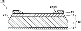
- the outer edge of the light shielding film 20 may be located inside the outer edge of the filter body 10 as in the near infrared cut filter 120 shown in FIG. In this case, it is preferable to form the chamfered portion 24 on the outer peripheral portion of the filter main body 10 like the near infrared cut filter 130 shown in FIG. By forming the chamfered portion 24, it is possible to suppress stray light generated by reflection of light incident on the exposed outer surface of the filter body 10.
- an infrared light absorption film 15 may be provided between the transparent substrate 11 and the antireflection film 13.
- the infrared light absorbing film 15 may be provided between the transparent substrate 11 and the ultraviolet / infrared light reflecting film 12.
- the infrared light absorbing film 15 can be made of a transparent resin containing an infrared absorber that absorbs light in the infrared wavelength region.
- the transparent resin only needs to transmit light in the visible wavelength region.
- acrylic resin styrene resin, ABS resin, AS resin, polycarbonate resin, polyolefin resin, polyvinyl chloride resin, acetate resin, cellulose resin Polyester resin, allyl ester resin, polyimide resin, polyamide resin, polyimide ether resin, polyamideimide resin, epoxy resin, urethane resin, urea resin, and the like.
- Infrared absorbers that absorb light in the infrared wavelength region include inorganic fine particles such as ITO (In 2 O 3 —TiO 2 system), ATO (ZnO—TiO 2 system), lanthanum boride, cyanine compounds, and phthalocyanine.
- organic dyes such as phthalocyanine compounds, naphthalocyanine compounds, dithiol metal complex compounds, diimonium compounds, polymethine compounds, phthalide compounds, naphthoquinone compounds, anthraquinone compounds, and indophenol compounds.
- the inorganic fine particles are composed of oxide crystallites containing at least Cu and / or P, and have a number average aggregate particle diameter of 5 to 200 nm, preferably a crystal of a compound represented by the following formula (1) Those having a number average aggregate particle diameter of 5 to 200 nm can be used.
- a 1 / n CuPO 4 (1) (In the formula, A is at least one selected from the group consisting of alkali metals (Li, Na, K, Rb, Cs), alkaline earth metals (Mg, Ca, Sr, Ba) and NH 4 ; N is 1 when A is an alkali metal or NH 4 and is 2 when A is an alkaline earth metal.)
- Those composed of crystallites can maintain the infrared absorption characteristics due to the crystal structure, and since the crystallites are fine particles, they can be contained in the infrared light absorption film 15 at a high concentration, and per unit length. It is preferable because the absorption capacity can be increased.
- the inorganic fine particles may be subjected to a surface treatment by a known method for the purpose of improving weather resistance, acid resistance, water resistance, etc. and improving compatibility with the binder resin by surface modification.
- an organic dye a dye having a maximum absorption peak having a peak wavelength of 695 ⁇ 1 nm and a full width at half maximum of 35 ⁇ 5 nm in an absorption spectrum of light having a wavelength region of 400 to 1000 nm measured by dissolving in acetone. Can be used. Such a dye is preferable because the absorbance changes abruptly in the vicinity of a wavelength of 630 to 700 nm required for a near infrared cut filter.
- Infrared absorbers may be used alone or in combination of two or more.
- the transparent resin further includes a color tone correction dye, a leveling agent, an antistatic agent, a heat stabilizer, an antioxidant, a dispersant, a flame retardant, and a lubricant as long as the effects of the present invention are not impaired.
- a plasticizer or the like may be contained.
- the infrared light absorption film 15 is prepared by, for example, preparing a coating liquid by dispersing or dissolving a transparent resin, an infrared absorber, and other additives blended as necessary in a dispersion medium or solvent. Then, it can be formed by drying. Coating and drying can be carried out in multiple steps. At that time, a plurality of coating liquids having different components may be prepared, and these may be sequentially coated and dried. Specifically, for example, a coating solution containing the above-mentioned organic dye and a coating solution containing ITO particles may be prepared separately, and these may be applied in order and dried.
- dispersion medium or solvent examples include water, alcohol, ketone, ether, ester, aldehyde, amine, aliphatic hydrocarbon, alicyclic hydrocarbon, aromatic hydrocarbon and the like. These may be used alone or in combination of two or more.
- a dispersing agent can be mix
- a stirring device such as a rotation / revolution mixer, a bead mill, a planetary mill, or an ultrasonic homogenizer can be used.
- a stirring device such as a rotation / revolution mixer, a bead mill, a planetary mill, or an ultrasonic homogenizer.
- spin coating method for coating of coating liquid, spin coating method, bar coating method, dip coating method, casting method, spray coating method, bead coating method, wire bar coating method, blade coating method, roller coating method, curtain coating method, slit A die coating method, a gravure coating method, a slit reverse coating method, a micro gravure method, a comma coating method, or the like can be used.
- the thickness of the infrared light absorbing film 15 is preferably in the range of 0.01 to 400 ⁇ m, more preferably in the range of 0.1 to 50 ⁇ m. If it is less than 0.01 ⁇ m, there is a possibility that a predetermined absorption capacity may not be obtained, and if it exceeds 400 ⁇ m, drying unevenness may occur during drying.
- the near infrared cut filter 130 provided with the infrared light absorbing film 15 can have a good near infrared cut function.
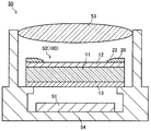
- FIG. 13 is a cross-sectional view schematically showing an imaging device 50 using the near-infrared cut filter of the present embodiment.
- the imaging device 50 includes a solid-state imaging device 51, an optical filter 52, a lens 53, and a housing 54 that holds and fixes them.
- the solid-state image sensor 51, the optical filter 52, and the lens 53 are disposed along the optical axis x, and the optical filter 52 is disposed between the solid-state image sensor 51 and the lens 53.
- the solid-state imaging device 51 is an electronic component that converts light incident through the lens 53 and the optical filter 52 into an electrical signal, and is, for example, a CCD or a CMOS.
- the near-infrared cut filter 100 shown in FIG. 1 is used as the optical filter 52, and the light shielding film 20 is disposed on the lens 53 side.
- the near-infrared cut filter 100 may be disposed so that the light shielding film 20 is positioned on the solid-state imaging device 51 side. Further, as the optical filter 52, the near-infrared cut filter shown in FIG. 9, FIG. 10, FIG. 11, FIG. Even when these near infrared cut filters are used, the light shielding film 20 may be disposed on the lens 53 side or may be disposed on the solid-state imaging device 51 side.
- the light incident from the subject side enters the solid-state imaging device 51 through the lens 53 and the optical filter 52 (near infrared cut filter 100).
- the solid-state image sensor 51 converts the incident light into an electric signal and outputs it as an image signal.
- Incident light passes through the near-infrared cut filter 100 provided with the light-shielding film 20, is adjusted to an appropriate amount of light, and is received by the solid-state imaging device 51 as light with sufficient near-infrared shielding.
- the near-infrared cut filter 100 is integrally provided with the light-shielding film 20 having the irregularities 22 and the thin-walled portion 23, so that light diffraction at the inner edge of the light-shielding film as in the prior art is performed.
- the resulting stray light can be suppressed, and a good image without noise can be obtained.
- the near-infrared cut filter 100 is preferably arranged so that the distance between the light-shielding film 20 and the light-receiving surface of the image sensor is 0.02 to 5 mm, from the viewpoints of diffraction suppression effect and manufacturing technology restrictions.
- the imaging device 50 is provided with only one lens, but may include a plurality of lenses, or a cover glass that protects the solid-state imaging device.
- the position of the optical filter is not limited to between the lens and the solid-state imaging device, and may be disposed on the subject side of the lens, for example. Also, when a plurality of lenses are disposed, between the lenses. May be arranged.
- the embodiment described above is an example of a filter in which the optical filter has a near-infrared cut function, but is not limited to the near-infrared cut function, and has functions such as a low-pass filter, an ND filter, a color tone filter, and an optical amplification filter. There may be.
- the present invention is not limited to the description of the embodiment described above, and it is needless to say that the present invention can be appropriately changed without departing from the gist of the present invention.
- Example 1 Silica (SiO 2 ; refractive index 1.45 (wavelength 550 nm)) is deposited on one surface of a 40 mm ⁇ 40 mm ⁇ 0.3 mm square plate-shaped infrared absorbing glass (NF-50 glass manufactured by Asahi Glass Co., Ltd.) by vacuum deposition. Layers and titania (TiO 2 ; refractive index 2.32 (wavelength 550 nm)) layers were alternately laminated to form a dielectric multilayer film (34 layers). An antireflection film was formed on the other surface of the infrared absorbing glass.
- a light-shielding UV curable acrylate resin is applied to the entire surface of the dielectric multilayer film to a thickness of 1.2 ⁇ m by a spin coating method, and after heating, irregular irregularities are formed on the inner peripheral surface of the opening on the surface. It was cured by irradiating with 100 mJ / cm 2 of ultraviolet light through a photomask having a high-pressure mercury lamp. Then, the unexposed part was removed using the developing solution, and it heated, and manufactured the near-infrared cut off filter.
- Irregular irregularities were formed on the inner peripheral surface of the light shielding film of the obtained near infrared cut filter. Further, when the surface of the light shielding film was observed with an atomic force microscope (AMF), a ridge-like fine uneven structure having an average interval (S) of 10 ⁇ m between the local peaks was formed, and the surface roughness of the light shielding film was arithmetic. The average roughness (Ra) was 180 nm.
- Example 2 In the same manner as in Example 1, a silica (SiO 2 ; refractive index 1.45 (wavelength 550 nm)) layer and titania (with a refractive index of 1.45 (wavelength 550 nm)) were formed on one surface of an infrared absorbing glass (NF-50 glass manufactured by Asahi Glass Co., Ltd.) by vacuum deposition. A dielectric multilayer film (34 layers) was formed by alternately laminating TiO 2 ; refractive index 2.32 (wavelength 550 nm) layers. A three-layer antireflection film was formed on the other surface of the infrared absorbing glass.
- silica (SiO 2 ; refractive index 1.45 (wavelength 550 nm)) layer and titania (with a refractive index of 1.45 (wavelength 550 nm) were formed on one surface of an infrared absorbing glass (NF-50 glass manufactured by Asahi Glass Co., Ltd.) by vacuum deposition.
- a light-shielding resin ink (containing black colored pigment), silica fine powder (average particle diameter (D50)) 4.7 ⁇ m) and a solvent were added and mixed uniformly to apply a coating solution prepared and heated to form a first coating film.
- the coating liquid is applied again on the first coating film and heated to form a second coating film.
- the near-infrared cut off filter provided with the 7-micrometer-thick light shielding film which consists of a 2nd coating film was manufactured.
- FIGS. 14A and 14B Irregular irregularities as shown in FIGS. 14A and 14B were formed on the inner peripheral surface of the light shielding film of the obtained near-infrared cut filter.
- FIG. 14A is a copy of a photograph taken by an optical microscope of the light shielding film
- FIG. 14B is a copy of the enlarged photograph.
- the arrow in FIG. 14B points to the convex portion formed on the inner peripheral surface of the light shielding film.
- the average roughness (Ra) is 0.43 ⁇ m
- the maximum height (Ry) is 3.63 ⁇ m
- the average distance between local peaks (S) is 30 ⁇ m
- arithmetic average roughness (Ra) 0.4 ⁇ m
- maximum height (Ry) 3.5 ⁇ m
- the average interval (S) was 5.0 ⁇ m.
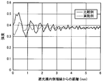
- the near-infrared cut filter was irradiated with light having a wavelength of 633 nm, and the light amount distribution of the transmitted light was examined using a beam profiler (manufactured by Offiel).
- a conventional near-infrared cut filter manufactured in the same manner as in Example 2 was also measured except that the unevenness and the thin portion were not formed on the light shielding film. The results are shown in FIG.
- the transmitted light intensity of the example is clearly reduced compared with the comparative example at the inner edge of the light shielding film and in the vicinity thereof, and the light shielding film is uneven and thin. By forming the portion, it is possible to prevent image deterioration due to diffraction.
- the optical filter of the present invention is excellent in productivity and economy and can be integrally provided with a light-shielding film having an effect of suppressing diffraction of light at the inner edge, so that a digital still camera, a digital video camera, a mobile phone, a notebook personal This is useful for an imaging apparatus such as a small camera incorporated in an information device such as a computer or PDA.
- SYMBOLS 10 ... (Near-infrared cut) Filter main body, 11 ... Transparent base material, 12 ... Ultraviolet / infrared light reflection film, 13 ... Antireflection film, 15 ... Infrared light absorption film, 20 ... Frame-shaped light shielding film, 22 ... Concavity and convexity , 23 ... Thin portion, 50 ... Imaging device, 51 ... Solid-state imaging device, 52 ... Optical filter, 53 ... Lens, 54 ... Housing, 100, 110, 120, 130, 140 ... Near-infrared cut filter.
Landscapes
- Physics & Mathematics (AREA)
- General Physics & Mathematics (AREA)
- Optics & Photonics (AREA)
- Health & Medical Sciences (AREA)
- Toxicology (AREA)
- Optical Filters (AREA)
- Optical Elements Other Than Lenses (AREA)
- Blocking Light For Cameras (AREA)
- Laminated Bodies (AREA)
- Solid State Image Pick-Up Elements (AREA)
Abstract
Description
(1)平面視で前記枠状遮光膜の内周面の少なくとも一部に凹凸が形成されている
(2)前記枠状遮光膜の内縁部の少なくとも一部に薄肉部が形成されている
図3は、凹凸22及び薄肉部23が形成されていない従来の遮光膜20Aを備えた近赤外線カットフィルタに光を入射させた場合の、遮光膜20Aとその近傍における光の透過と、その透過した光の量を概念的に示した図である。また、図4は、図1に示すような、凹凸22及び薄肉部23が形成された遮光膜20を備えた近赤外線カットフィルタ100に光を入射させた場合の、遮光膜20とその近傍における光の透過と、その透過した光の量を概念的に示した図である。
まず、フィルタ本体10の紫外・赤外光反射膜12の表面全体に、遮光性を有する光硬化性樹脂を塗布し乾燥させて光硬化性樹脂塗布層を形成する。光硬化性樹脂の塗布方法としては、スピンコート法、バーコート法、ディップコート法、キャスト法、スプレーコート法、ビードコート法、ワイヤーバーコート法、ブレードコート法、ローラーコート法、カーテンコート法、スリットダイコート法、グラビアコート法、スリットリバースコート法、マイクログラビア法、コンマコート法等を使用できる。塗布は、複数回に分けて実施してもよい。また、塗布に先立って、紫外・赤外光反射膜12に対する密着性を高めるために、紫外・赤外光反射膜12の表面にヘキサメチルジシラザン(HMDS)等によるカップリング処理を行ってもよい。
上記と同様に形成した光硬化性樹脂塗布層に、遮光膜20に対応する位置を開口させるとともに、その開口の内周面に凹凸22に対応する形状の凹凸を設けた第1のフォトマスクを介して、1回目の光を照射する。さらに、その開口の内周面より薄肉部23の幅wだけ小さな開口を設けた第2のフォトマスクを介して2回目の光を照射する。1回目の光照射によっては、光硬化性樹脂を完全に硬化させず、2回目の光照射によって硬化を完了させる。この後、未照射部の光硬化性樹脂を現像により選択的に除去すると、1回目の光照射のみがなされた部分は光による硬化が不十分なため、2回目の光照射を行った部分より光硬化性樹脂の厚みが薄くなり、薄肉部23を形成できる。この例では2つのフォトマスクを用いているが、開口の幅が徐々に小さくなっている3つもしくはそれ以上のフォトマスクを用いて光照射を繰り返すようにすれば、厚みが端縁に向けて漸減する薄肉部23を形成できる。
遮光膜20に対応する位置を開口させた第1のスクリーン版を介して、1回目の遮光性樹脂を印刷し硬化させる。次に、その開口の内周面より薄肉部23の幅wだけ小さな開口を設けた第2のスクリーン版を介して2回目の遮光性樹脂を印刷し硬化させる。これにより、内縁部に薄肉部23を備えた遮光膜20を形成できる。
また、印刷時にスクリーン版とフィルタ本体10のクリアランスを、少し大きめに調整したり、スキージの圧力・角度などを調整したりすることでも薄肉部23を形成できる。
さらに、内周面に形成する凹凸22とは別に、より細かなピッチの凹凸を内周面に相当する部分のスクリーン版に設けることにより、印刷時にスクリーン版の開口部に対して細かなピッチの凹凸がある部分からの遮光性樹脂が出にくくなり、遮光性樹脂の厚みを小さくでき、薄肉部23を形成できる。
A1/nCuPO4 …(1)
(式中、Aは、アルカリ金属(Li、Na、K、Rb、Cs)、アルカリ土類金属(Mg、Ca、Sr、Ba)及びNH4からなる群より選ばれる少なくとも1種であり、添字のnは、Aがアルカリ金属またはNH4の場合は1であり、Aがアルカリ土類金属の場合は2である。)
図13に示すように、撮像装置50は、固体撮像素子51、光学フィルタ52、レンズ53、及びこれらを保持固定する筺体54を有する。
40mm×40mm×0.3mmの角板状の赤外線吸収ガラス(NF-50ガラス 旭硝子社製)の一方の表面に、真空蒸着法により、シリカ(SiO2;屈折率1.45(波長550nm))層とチタニア(TiO2;屈折率2.32(波長550nm))層とを交互に積層して誘電体多層膜(34層)を形成した。また、赤外線吸収ガラスの他方の表面に反射防止膜を形成した。
実施例1と同様にして、赤外線吸収ガラス(NF-50ガラス 旭硝子社製)の一方の表面に、真空蒸着法により、シリカ(SiO2;屈折率1.45(波長550nm))層とチタニア(TiO2;屈折率2.32(波長550nm))層とを交互に積層して誘電体多層膜(34層)を形成した。また、赤外線吸収ガラスの他方の表面に3層反射防止膜を形成した。
Claims (9)
- 被写体または光源からの光が入射する撮像素子が内蔵された撮像装置に用いられる光学フィルタであって、
前記被写体または光源と前記撮像素子との間に配置され、前記入射光に対し透過性を有する光学フィルタ本体と、
前記光学フィルタ本体の少なくとも一方の面に一体に形成された枠状遮光膜と
を備え、
前記枠状遮光膜は、下記(1)及び/または(2)の条件を満たしていることを特徴とする光学フィルタ。
(1)平面視で前記枠状遮光膜の内周面の少なくとも一部に凹凸が形成されている。
(2)前記枠状遮光膜の内縁部の少なくとも一部に薄肉部が形成されている。 - 前記凹凸は、不規則な凹凸である請求項1記載の光学フィルタ。
- 前記凹凸は、平面視の測定で、0.4~50μmの高さを有する請求項1または2記載の光学フィルタ。
- 前記薄肉部の光透過率が0.5%以上である請求項1乃至3のいずれか1項記載の光学フィルタ。
- 前記薄肉部の幅は、0.4~50μmである請求項4記載の光学フィルタ。
- 前記薄肉部は、端縁に向けて徐々に厚さが薄くなる傾斜面を有する請求項1乃至5のいずれか1項記載の光学フィルタ。
- 近赤外線カット機能を有する光学フィルタである請求項1乃至6のいずれか1項記載の光学フィルタ。
- 前記光学フィルタ本体は、赤外波長領域の光を吸収する赤外線吸収ガラスを備える請求項1乃至7のいずれか1項記載の光学フィルタ。
- 前記光学フィルタ本体は、赤外波長領域の光を吸収する赤外線吸収剤を含む赤外光吸収膜を備える請求項1乃至8のいずれか1項記載の光学フィルタ。
Priority Applications (4)
| Application Number | Priority Date | Filing Date | Title |
|---|---|---|---|
| KR1020137027511A KR101467139B1 (ko) | 2012-08-03 | 2013-07-29 | 광학 필터 |
| CN201380001236.0A CN103718069B (zh) | 2012-08-03 | 2013-07-29 | 滤光器 |
| JP2013543437A JP6330329B2 (ja) | 2012-08-03 | 2013-07-29 | 光学フィルタ |
| US14/548,890 US9759847B2 (en) | 2012-08-03 | 2014-11-20 | Optical filter |
Applications Claiming Priority (2)
| Application Number | Priority Date | Filing Date | Title |
|---|---|---|---|
| JP2012-173319 | 2012-08-03 | ||
| JP2012173319 | 2012-08-03 |
Related Child Applications (1)
| Application Number | Title | Priority Date | Filing Date |
|---|---|---|---|
| US14/548,890 Continuation US9759847B2 (en) | 2012-08-03 | 2014-11-20 | Optical filter |
Publications (1)
| Publication Number | Publication Date |
|---|---|
| WO2014021245A1 true WO2014021245A1 (ja) | 2014-02-06 |
Family
ID=50027920
Family Applications (1)
| Application Number | Title | Priority Date | Filing Date |
|---|---|---|---|
| PCT/JP2013/070432 Ceased WO2014021245A1 (ja) | 2012-08-03 | 2013-07-29 | 光学フィルタ |
Country Status (5)
| Country | Link |
|---|---|
| US (1) | US9759847B2 (ja) |
| JP (3) | JP6330329B2 (ja) |
| KR (1) | KR101467139B1 (ja) |
| CN (1) | CN103718069B (ja) |
| WO (1) | WO2014021245A1 (ja) |
Cited By (10)
| Publication number | Priority date | Publication date | Assignee | Title |
|---|---|---|---|---|
| WO2016159045A1 (ja) * | 2015-03-30 | 2016-10-06 | Scivax株式会社 | 反射防止構造体 |
| JP2017191169A (ja) * | 2016-04-12 | 2017-10-19 | キヤノン株式会社 | 光学素子およびその製造方法 |
| JP2019010871A (ja) * | 2017-06-29 | 2019-01-24 | Agc株式会社 | 加飾層付き透明板、および表示装置 |
| JP2019191447A (ja) * | 2018-04-27 | 2019-10-31 | 東洋インキScホールディングス株式会社 | ブラックマトリクス基板、その製造方法、及び該基板を有する画像表示装置 |
| JP2020038338A (ja) * | 2018-08-29 | 2020-03-12 | 株式会社豊田中央研究所 | 光学フィルター及びその製造方法 |
| JP2020140168A (ja) * | 2019-03-01 | 2020-09-03 | 株式会社きもと | レンズ用スペーサー、並びに、これを用いた積層遮光部材、遮光リング、レンズユニット及びカメラモジュール |
| TWI730182B (zh) * | 2016-09-30 | 2021-06-11 | 日商住友化學股份有限公司 | 光學膜及光學膜的製造方法 |
| JP2022018835A (ja) * | 2020-07-16 | 2022-01-27 | 東芝テック株式会社 | 光学アレイ、光学装置及び画像形成装置 |
| JP2022074900A (ja) * | 2020-11-05 | 2022-05-18 | 凸版印刷株式会社 | 赤外線パスフィルター、着色性組成物、固体撮像素子用フィルターおよび固体撮像素子 |
| WO2023162900A1 (ja) * | 2022-02-25 | 2023-08-31 | Agc株式会社 | ガラス積層体、およびガラス積層体の製造方法 |
Families Citing this family (24)
| Publication number | Priority date | Publication date | Assignee | Title |
|---|---|---|---|---|
| CN103718069B (zh) * | 2012-08-03 | 2016-05-04 | 旭硝子株式会社 | 滤光器 |
| US9627426B2 (en) | 2014-02-27 | 2017-04-18 | Taiwan Semiconductor Manufacturing Co., Ltd. | Image sensor device and method for forming the same |
| US10276620B2 (en) | 2014-02-27 | 2019-04-30 | Taiwan Semiconductor Manufacturing Co., Ltd. | Image sensor device and method for forming the same |
| US9324752B2 (en) * | 2014-02-27 | 2016-04-26 | Taiwan Semiconductor Manufacturing Co., Ltd. | Image sensor device with light blocking structure |
| KR20160064640A (ko) * | 2014-11-28 | 2016-06-08 | 삼성전기주식회사 | 카메라 모듈 |
| JP6707966B2 (ja) * | 2016-04-18 | 2020-06-10 | 日本電気硝子株式会社 | 遮光プレート |
| CN108508679B (zh) * | 2017-02-24 | 2020-12-18 | 大立光电股份有限公司 | 遮光片、光学镜片组、成像镜头与电子装置 |
| US12501787B2 (en) | 2019-04-03 | 2025-12-16 | Boe Technology Group Co., Ltd. | Display panel and display device with curved light-shielding portions |
| US11489032B2 (en) | 2019-04-03 | 2022-11-01 | Boe Technology Group Co., Ltd. | Display panel and display device with light shielding portions having curved profile |
| KR102792607B1 (ko) | 2019-07-22 | 2025-04-09 | 삼성디스플레이 주식회사 | 윈도우 부재, 이를 포함하는 전자 장치 및 윈도우 부재의 제조 방법 |
| US11899225B2 (en) | 2019-08-30 | 2024-02-13 | Samsung Electro-Mechanics Co., Ltd. | Camera module |
| US10924705B1 (en) | 2019-12-31 | 2021-02-16 | Christie Digital Systems Usa, Inc. | Serrated prism exit aperture for managing projection flare artifacts |
| KR102569310B1 (ko) | 2020-05-15 | 2023-08-22 | 다이니폰 인사츠 가부시키가이샤 | 방현 필름 및 화상 표시 장치 |
| JP7511523B2 (ja) * | 2020-05-15 | 2024-07-05 | 大日本印刷株式会社 | 防眩フィルム及び画像表示装置 |
| CN111882995B (zh) * | 2020-08-31 | 2022-03-29 | 武汉天马微电子有限公司 | 显示面板及显示装置 |
| KR102613873B1 (ko) * | 2021-04-30 | 2023-12-15 | 삼성전기주식회사 | 카메라 모듈 |
| TWI783557B (zh) * | 2021-06-28 | 2022-11-11 | 大立光電股份有限公司 | 遮光片、成像鏡頭及電子裝置 |
| TWI855470B (zh) | 2021-07-16 | 2024-09-11 | 大立光電股份有限公司 | 透鏡組、光學裝置與電子裝置 |
| TWI820621B (zh) * | 2022-01-28 | 2023-11-01 | 大立光電股份有限公司 | 成像鏡頭及電子裝置 |
| JP2024029452A (ja) * | 2022-08-22 | 2024-03-06 | Toppanホールディングス株式会社 | 遮光膜及びこれを利用する赤外線センサ |
| TWI858701B (zh) * | 2023-05-12 | 2024-10-11 | 光寶科技股份有限公司 | 感測封裝結構 |
| CN119781140A (zh) * | 2023-08-09 | 2025-04-08 | Oppo广东移动通信有限公司 | 光学传导元件、拍摄模组及电子设备 |
| CN117975822A (zh) * | 2024-01-31 | 2024-05-03 | 昆山国显光电有限公司 | 显示模组、显示模组的制作方法及电子设备 |
| CN118330795A (zh) * | 2024-05-13 | 2024-07-12 | 维沃移动通信有限公司 | 光学元件、摄像模组及电子设备 |
Citations (5)
| Publication number | Priority date | Publication date | Assignee | Title |
|---|---|---|---|---|
| JPS5685968U (ja) * | 1979-12-06 | 1981-07-10 | ||
| JP2003248107A (ja) * | 2002-02-22 | 2003-09-05 | Olympus Optical Co Ltd | Ndフィルタ及びその製造方法とそれを用いたマルチディスプレイ装置及び画像生成装置 |
| JP2006259048A (ja) * | 2005-03-16 | 2006-09-28 | Seiko Epson Corp | 減光装置、プロジェクションシステム、およびプロジェクタ |
| JP2008070827A (ja) * | 2006-09-15 | 2008-03-27 | Agc Techno Glass Co Ltd | 赤外線遮蔽フィルタ |
| JP2009244529A (ja) * | 2008-03-31 | 2009-10-22 | Konica Minolta Opto Inc | 遮光部及びレンズ鏡胴 |
Family Cites Families (15)
| Publication number | Priority date | Publication date | Assignee | Title |
|---|---|---|---|---|
| JPS5685968A (en) | 1979-12-14 | 1981-07-13 | Hitachi Ltd | Channel switching system |
| JP2002042551A (ja) | 2000-07-21 | 2002-02-08 | Murata Mfg Co Ltd | スクリーン印刷用ペースト、スクリーン印刷方法及び厚膜焼成体 |
| JP2002268120A (ja) * | 2001-03-14 | 2002-09-18 | Kureha Chem Ind Co Ltd | 光学的機能フィルター部材及び撮像装置 |
| CN1220089C (zh) * | 2002-06-27 | 2005-09-21 | 奥林巴斯株式会社 | 摄像透镜单元和摄像装置及其制造方法 |
| US20060121392A1 (en) * | 2004-11-24 | 2006-06-08 | Dai Nippon Printing Co., Ltd. | Optical filter and display using the same |
| JP4818721B2 (ja) * | 2005-12-28 | 2011-11-16 | キヤノン電子株式会社 | 光学部材 |
| JP5058847B2 (ja) * | 2007-03-07 | 2012-10-24 | 富士フイルム株式会社 | 光学フィルタ、及びそれを用いた液晶表示装置 |
| JP5226330B2 (ja) | 2008-01-25 | 2013-07-03 | 株式会社ジャパンディスプレイイースト | 液晶表示装置 |
| JP2010175749A (ja) * | 2009-01-28 | 2010-08-12 | Nippon Shokubai Co Ltd | 樹脂フィルムの製造方法 |
| JP5410473B2 (ja) * | 2011-06-08 | 2014-02-05 | キヤノン電子株式会社 | 光学部材 |
| WO2013061990A1 (ja) | 2011-10-24 | 2013-05-02 | 旭硝子株式会社 | 光学フィルタとその製造方法、並びに撮像装置 |
| US20130175650A1 (en) * | 2012-01-05 | 2013-07-11 | Apple Inc | Cover for image sensor assembly with light absorbing layer |
| JP2013207035A (ja) | 2012-03-28 | 2013-10-07 | Sony Corp | 撮像素子、製造装置および方法、撮像装置、表示素子、並びに表示装置 |
| CN103718069B (zh) * | 2012-08-03 | 2016-05-04 | 旭硝子株式会社 | 滤光器 |
| MX366455B (es) | 2015-01-27 | 2019-07-10 | Teikoku Printing Inks Mfg Co Ltd | Composicion de tinta para serigrafia de alta calidad/alta definicion, material impreso producido por la composicion de tinta de serigrafia, y metodo para producir el material impreso. |
-
2013
- 2013-07-29 CN CN201380001236.0A patent/CN103718069B/zh active Active
- 2013-07-29 KR KR1020137027511A patent/KR101467139B1/ko active Active
- 2013-07-29 WO PCT/JP2013/070432 patent/WO2014021245A1/ja not_active Ceased
- 2013-07-29 JP JP2013543437A patent/JP6330329B2/ja active Active
-
2014
- 2014-11-20 US US14/548,890 patent/US9759847B2/en active Active
-
2018
- 2018-02-19 JP JP2018027092A patent/JP6525077B2/ja active Active
- 2018-02-19 JP JP2018027093A patent/JP6525078B2/ja active Active
Patent Citations (5)
| Publication number | Priority date | Publication date | Assignee | Title |
|---|---|---|---|---|
| JPS5685968U (ja) * | 1979-12-06 | 1981-07-10 | ||
| JP2003248107A (ja) * | 2002-02-22 | 2003-09-05 | Olympus Optical Co Ltd | Ndフィルタ及びその製造方法とそれを用いたマルチディスプレイ装置及び画像生成装置 |
| JP2006259048A (ja) * | 2005-03-16 | 2006-09-28 | Seiko Epson Corp | 減光装置、プロジェクションシステム、およびプロジェクタ |
| JP2008070827A (ja) * | 2006-09-15 | 2008-03-27 | Agc Techno Glass Co Ltd | 赤外線遮蔽フィルタ |
| JP2009244529A (ja) * | 2008-03-31 | 2009-10-22 | Konica Minolta Opto Inc | 遮光部及びレンズ鏡胴 |
Cited By (16)
| Publication number | Priority date | Publication date | Assignee | Title |
|---|---|---|---|---|
| JPWO2016159045A1 (ja) * | 2015-03-30 | 2018-01-25 | Scivax株式会社 | 反射防止構造体 |
| WO2016159045A1 (ja) * | 2015-03-30 | 2016-10-06 | Scivax株式会社 | 反射防止構造体 |
| JP2017191169A (ja) * | 2016-04-12 | 2017-10-19 | キヤノン株式会社 | 光学素子およびその製造方法 |
| TWI730182B (zh) * | 2016-09-30 | 2021-06-11 | 日商住友化學股份有限公司 | 光學膜及光學膜的製造方法 |
| JP2019010871A (ja) * | 2017-06-29 | 2019-01-24 | Agc株式会社 | 加飾層付き透明板、および表示装置 |
| JP6992689B2 (ja) | 2017-06-29 | 2022-02-03 | Agc株式会社 | 加飾層付き透明板、および表示装置 |
| JP2019191447A (ja) * | 2018-04-27 | 2019-10-31 | 東洋インキScホールディングス株式会社 | ブラックマトリクス基板、その製造方法、及び該基板を有する画像表示装置 |
| JP2020038338A (ja) * | 2018-08-29 | 2020-03-12 | 株式会社豊田中央研究所 | 光学フィルター及びその製造方法 |
| JP7342390B2 (ja) | 2018-08-29 | 2023-09-12 | 株式会社デンソーウェーブ | 光学フィルター及びその製造方法 |
| WO2020179560A1 (ja) * | 2019-03-01 | 2020-09-10 | 株式会社きもと | レンズ用スペーサー、並びに、これを用いた積層遮光部材、遮光リング、レンズユニット及びカメラモジュール |
| JP2020140168A (ja) * | 2019-03-01 | 2020-09-03 | 株式会社きもと | レンズ用スペーサー、並びに、これを用いた積層遮光部材、遮光リング、レンズユニット及びカメラモジュール |
| JP7396803B2 (ja) | 2019-03-01 | 2023-12-12 | 株式会社きもと | レンズ用スペーサー、並びに、これを用いた積層遮光部材、遮光リング、レンズユニット及びカメラモジュール |
| JP2022018835A (ja) * | 2020-07-16 | 2022-01-27 | 東芝テック株式会社 | 光学アレイ、光学装置及び画像形成装置 |
| JP7451334B2 (ja) | 2020-07-16 | 2024-03-18 | 東芝テック株式会社 | 光学アレイ、光学装置及び画像形成装置 |
| JP2022074900A (ja) * | 2020-11-05 | 2022-05-18 | 凸版印刷株式会社 | 赤外線パスフィルター、着色性組成物、固体撮像素子用フィルターおよび固体撮像素子 |
| WO2023162900A1 (ja) * | 2022-02-25 | 2023-08-31 | Agc株式会社 | ガラス積層体、およびガラス積層体の製造方法 |
Also Published As
| Publication number | Publication date |
|---|---|
| KR101467139B1 (ko) | 2014-11-28 |
| CN103718069A (zh) | 2014-04-09 |
| JP6525078B2 (ja) | 2019-06-05 |
| JP2018092188A (ja) | 2018-06-14 |
| US9759847B2 (en) | 2017-09-12 |
| KR20140033355A (ko) | 2014-03-18 |
| JP6330329B2 (ja) | 2018-05-30 |
| JP6525077B2 (ja) | 2019-06-05 |
| JPWO2014021245A1 (ja) | 2016-07-21 |
| JP2018116285A (ja) | 2018-07-26 |
| CN103718069B (zh) | 2016-05-04 |
| US20150077841A1 (en) | 2015-03-19 |
Similar Documents
| Publication | Publication Date | Title |
|---|---|---|
| JP6330329B2 (ja) | 光学フィルタ | |
| KR101483386B1 (ko) | 광학 필터와 그의 제조 방법, 및 촬상 장치 | |
| JP5741347B2 (ja) | 光学フィルタ及びこれを用いた撮像装置 | |
| JP5849719B2 (ja) | 光吸収体及びこれを用いた撮像装置 | |
| JP6790831B2 (ja) | 光学フィルタ及び撮像装置 | |
| EP3937246B1 (en) | Lens sheet, lens sheet unit, imaging module, imaging device | |
| WO2014021232A1 (ja) | マイクロレンズアレイ、撮像素子パッケージおよびマイクロレンズアレイの製造方法 | |
| US20100040865A1 (en) | Optical filter and method for manufacturing same | |
| JP2013114103A (ja) | 光学系および光学機器 | |
| JP2017167557A (ja) | 光吸収体及びこれを用いた撮像装置 | |
| JP2016015479A (ja) | 光学素子 | |
| CN203551813U (zh) | 近红外线截止滤波器 | |
| JP6556529B2 (ja) | 光学フィルタ、及び、光学フィルタを備えた光学装置 | |
| JP6304254B2 (ja) | 光学部材とその製造方法、並びに撮像装置 | |
| JP6156468B2 (ja) | 光吸収体及びこれを用いた撮像装置 | |
| WO2022067951A1 (zh) | 摄像镜头 | |
| JP2013114098A (ja) | 光学素子、光学系および光学機器 | |
| JP6980364B2 (ja) | 光学フィルタ及び光量調整装置並びに光学装置 |
Legal Events
| Date | Code | Title | Description |
|---|---|---|---|
| WWE | Wipo information: entry into national phase |
Ref document number: 201380001236.0 Country of ref document: CN |
|
| ENP | Entry into the national phase |
Ref document number: 2013543437 Country of ref document: JP Kind code of ref document: A |
|
| ENP | Entry into the national phase |
Ref document number: 20137027511 Country of ref document: KR Kind code of ref document: A |
|
| 121 | Ep: the epo has been informed by wipo that ep was designated in this application |
Ref document number: 13826161 Country of ref document: EP Kind code of ref document: A1 |
|
| NENP | Non-entry into the national phase |
Ref country code: DE |
|
| 122 | Ep: pct application non-entry in european phase |
Ref document number: 13826161 Country of ref document: EP Kind code of ref document: A1 |