WO2014021035A1 - Dcdcコンバータ - Google Patents
Dcdcコンバータ Download PDFInfo
- Publication number
- WO2014021035A1 WO2014021035A1 PCT/JP2013/067763 JP2013067763W WO2014021035A1 WO 2014021035 A1 WO2014021035 A1 WO 2014021035A1 JP 2013067763 W JP2013067763 W JP 2013067763W WO 2014021035 A1 WO2014021035 A1 WO 2014021035A1
- Authority
- WO
- WIPO (PCT)
- Prior art keywords
- side switching
- low voltage
- switching circuit
- voltage side
- circuit unit
- Prior art date
- Legal status (The legal status is an assumption and is not a legal conclusion. Google has not performed a legal analysis and makes no representation as to the accuracy of the status listed.)
- Ceased
Links
Images






Classifications
-
- H—ELECTRICITY
- H02—GENERATION; CONVERSION OR DISTRIBUTION OF ELECTRIC POWER
- H02M—APPARATUS FOR CONVERSION BETWEEN AC AND AC, BETWEEN AC AND DC, OR BETWEEN DC AND DC, AND FOR USE WITH MAINS OR SIMILAR POWER SUPPLY SYSTEMS; CONVERSION OF DC OR AC INPUT POWER INTO SURGE OUTPUT POWER; CONTROL OR REGULATION THEREOF
- H02M3/00—Conversion of DC power input into DC power output
- H02M3/22—Conversion of DC power input into DC power output with intermediate conversion into AC
- H02M3/24—Conversion of DC power input into DC power output with intermediate conversion into AC by static converters
- H02M3/28—Conversion of DC power input into DC power output with intermediate conversion into AC by static converters using discharge tubes with control electrode or semiconductor devices with control electrode to produce the intermediate AC
- H02M3/325—Conversion of DC power input into DC power output with intermediate conversion into AC by static converters using discharge tubes with control electrode or semiconductor devices with control electrode to produce the intermediate AC using devices of a triode or a transistor type requiring continuous application of a control signal
- H02M3/335—Conversion of DC power input into DC power output with intermediate conversion into AC by static converters using discharge tubes with control electrode or semiconductor devices with control electrode to produce the intermediate AC using devices of a triode or a transistor type requiring continuous application of a control signal using semiconductor devices only
- H02M3/33507—Conversion of DC power input into DC power output with intermediate conversion into AC by static converters using discharge tubes with control electrode or semiconductor devices with control electrode to produce the intermediate AC using devices of a triode or a transistor type requiring continuous application of a control signal using semiconductor devices only with automatic control of the output voltage or current, e.g. flyback converters
-
- H—ELECTRICITY
- H05—ELECTRIC TECHNIQUES NOT OTHERWISE PROVIDED FOR
- H05K—PRINTED CIRCUITS; CASINGS OR CONSTRUCTIONAL DETAILS OF ELECTRIC APPARATUS; MANUFACTURE OF ASSEMBLAGES OF ELECTRICAL COMPONENTS
- H05K7/00—Constructional details common to different types of electric apparatus
- H05K7/20—Modifications to facilitate cooling, ventilating, or heating
- H05K7/2089—Modifications to facilitate cooling, ventilating, or heating for power electronics, e.g. for inverters for controlling motor
- H05K7/20927—Liquid coolant without phase change
-
- H—ELECTRICITY
- H05—ELECTRIC TECHNIQUES NOT OTHERWISE PROVIDED FOR
- H05K—PRINTED CIRCUITS; CASINGS OR CONSTRUCTIONAL DETAILS OF ELECTRIC APPARATUS; MANUFACTURE OF ASSEMBLAGES OF ELECTRICAL COMPONENTS
- H05K9/00—Screening of apparatus or components against electric or magnetic fields
- H05K9/0007—Casings
- H05K9/002—Casings with localised screening
- H05K9/0022—Casings with localised screening of components mounted on printed circuit boards [PCB]
- H05K9/0037—Housings with compartments containing a PCB, e.g. partitioning walls
-
- H—ELECTRICITY
- H02—GENERATION; CONVERSION OR DISTRIBUTION OF ELECTRIC POWER
- H02M—APPARATUS FOR CONVERSION BETWEEN AC AND AC, BETWEEN AC AND DC, OR BETWEEN DC AND DC, AND FOR USE WITH MAINS OR SIMILAR POWER SUPPLY SYSTEMS; CONVERSION OF DC OR AC INPUT POWER INTO SURGE OUTPUT POWER; CONTROL OR REGULATION THEREOF
- H02M1/00—Details of apparatus for conversion
- H02M1/44—Circuits or arrangements for compensating for electromagnetic interference in converters or inverters
-
- H—ELECTRICITY
- H02—GENERATION; CONVERSION OR DISTRIBUTION OF ELECTRIC POWER
- H02M—APPARATUS FOR CONVERSION BETWEEN AC AND AC, BETWEEN AC AND DC, OR BETWEEN DC AND DC, AND FOR USE WITH MAINS OR SIMILAR POWER SUPPLY SYSTEMS; CONVERSION OF DC OR AC INPUT POWER INTO SURGE OUTPUT POWER; CONTROL OR REGULATION THEREOF
- H02M3/00—Conversion of DC power input into DC power output
- H02M3/22—Conversion of DC power input into DC power output with intermediate conversion into AC
- H02M3/24—Conversion of DC power input into DC power output with intermediate conversion into AC by static converters
- H02M3/28—Conversion of DC power input into DC power output with intermediate conversion into AC by static converters using discharge tubes with control electrode or semiconductor devices with control electrode to produce the intermediate AC
- H02M3/325—Conversion of DC power input into DC power output with intermediate conversion into AC by static converters using discharge tubes with control electrode or semiconductor devices with control electrode to produce the intermediate AC using devices of a triode or a transistor type requiring continuous application of a control signal
- H02M3/335—Conversion of DC power input into DC power output with intermediate conversion into AC by static converters using discharge tubes with control electrode or semiconductor devices with control electrode to produce the intermediate AC using devices of a triode or a transistor type requiring continuous application of a control signal using semiconductor devices only
- H02M3/33569—Conversion of DC power input into DC power output with intermediate conversion into AC by static converters using discharge tubes with control electrode or semiconductor devices with control electrode to produce the intermediate AC using devices of a triode or a transistor type requiring continuous application of a control signal using semiconductor devices only having several active switching elements
- H02M3/33576—Conversion of DC power input into DC power output with intermediate conversion into AC by static converters using discharge tubes with control electrode or semiconductor devices with control electrode to produce the intermediate AC using devices of a triode or a transistor type requiring continuous application of a control signal using semiconductor devices only having several active switching elements having at least one active switching element at the secondary side of an isolation transformer
-
- Y—GENERAL TAGGING OF NEW TECHNOLOGICAL DEVELOPMENTS; GENERAL TAGGING OF CROSS-SECTIONAL TECHNOLOGIES SPANNING OVER SEVERAL SECTIONS OF THE IPC; TECHNICAL SUBJECTS COVERED BY FORMER USPC CROSS-REFERENCE ART COLLECTIONS [XRACs] AND DIGESTS
- Y02—TECHNOLOGIES OR APPLICATIONS FOR MITIGATION OR ADAPTATION AGAINST CLIMATE CHANGE
- Y02T—CLIMATE CHANGE MITIGATION TECHNOLOGIES RELATED TO TRANSPORTATION
- Y02T10/00—Road transport of goods or passengers
- Y02T10/60—Other road transportation technologies with climate change mitigation effect
- Y02T10/70—Energy storage systems for electromobility, e.g. batteries
Definitions
- the present invention relates to a DCDC converter device, and more particularly to a DCDC converter device applied to an electric vehicle and a plug-in hybrid vehicle.
- An electric vehicle and a plug-in hybrid vehicle are equipped with a high voltage storage battery or a low voltage storage battery.
- the high voltage storage battery is used as a power drive for driving a motor via an inverter device
- the low voltage storage battery is a vehicle light. Used to operate auxiliary equipment such as radio and radio.
- Such a vehicle is equipped with a DCDC converter device that performs power conversion from a high voltage storage battery to a low voltage storage battery or power conversion from a low voltage storage battery to a high voltage storage battery.
- An object of the present invention is to provide a device that reduces noise superposition emitted from a circuit and ensures a noise reduction effect of a filter.
- the DCDC converter device includes a transformer, a high-voltage side switching circuit unit electrically disposed between the transformer and the high-voltage side circuit unit, and between the transformer and the low-voltage side circuit unit.
- a metal case that houses the low-side switching circuit unit, the low-voltage side switching circuit unit, and the noise filter circuit unit
- a drive circuit board that has a drive circuit that drives the low-voltage side switching circuit unit, and the drive circuit A metal base plate on which a substrate is mounted, and the case is disposed between the low-voltage side switching circuit unit and the noise filter circuit unit.
- the base plate is disposed at a position facing the bottom surface of the case across the low voltage side switching circuit portion, and the partition plate is formed of the base plate. It is connected with.
- the influence of the noise current on the filter circuit unit can be reduced.
- FIG. 1 is a diagram illustrating a circuit configuration of a DCDC converter device 100.
- FIG. 4 is an exploded perspective view for explaining a component arrangement in the DCDC converter device 100.
- FIG. 2 is an exploded perspective view of a high voltage circuit 106.
- FIG. 2 is an exploded perspective view for explaining an internal configuration of a DCDC converter device 100.
- FIG. 2 is a plan view showing the inside of a DCDC converter device 100.
- FIG. FIG. 5 is a cross-sectional view of the AA cross section of FIG. 3 is a perspective view showing a low voltage substrate 107 in the DCDC converter device 100.
- FIG. 2 is a perspective view showing a filter substrate 120 in the DCDC converter device 100.
- FIG. 10 is a cross-sectional view of the AA cross section of FIG.
- FIG. 5 is a cross-sectional view of the DD cross section of FIG.
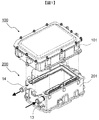
- FIG. 1 is a perspective view showing an external appearance of the power converter.
- the power conversion device is an integration of the DCDC converter device 100 and the inverter device 200.
- FIG. 1 shows the DCDC converter device 100 and the inverter device 200 in a separated state.
- the DCDC converter device 100 is fixed to the case bottom surface side of the inverter device 200 by a plurality of bolts (not shown).
- This power conversion device is applied to an electric vehicle or the like, and the inverter device 200 drives a traveling motor with electric power from an on-vehicle high voltage storage battery.
- the vehicle is equipped with a low voltage storage battery for operating auxiliary equipment such as a light and a radio, and the DCDC converter device 100 converts power from a high voltage storage battery to a low voltage storage battery or from a low voltage storage battery to a high voltage storage battery. Power conversion.
- a refrigerant flow path through which a refrigerant flows is formed in the side wall of the case 201 of the inverter device 200.
- the refrigerant flows into the flow path from the inlet pipe 13 and flows out from the outlet pipe 14.
- the case 101 of the DCDC converter device 100 faces the bottom surface of the inverter device 200 and is fixed without a gap. In the fixed state, the DCDC converter device 100 is also configured to use the refrigerant flow path.
- water is generally suitable as the refrigerant, but it can be used even if it is other than water.
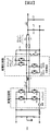
- FIG. 2 is a diagram illustrating a circuit configuration of the DCDC converter device 100.
- the DCDC converter apparatus 100 of this Embodiment it is bi-directional DCDC conversion which mutually converts the voltage between a low voltage storage battery and a high voltage storage battery.
- the high voltage circuit is composed of an H bridge circuit
- the low voltage circuit is composed of a synchronous rectifier circuit and an active clamp circuit.
- large current components are employed in the switching element and the smoothing coil is enlarged.
- an H-bridge type switching circuit configuration (H1 to H4) using a MOSFET having a freewheeling diode was adopted.
- an LC circuit (Cr, Lr) is used to perform zero voltage switching at a high switching frequency (100 kHz) to reduce switching loss and improve conversion efficiency.
- an IGBT switch (H0) is provided as a changeover switch that is turned on during step-down mode operation and turned off during step-up mode operation.
- a synchronous rectification circuit using a MOSFET and a full-wave rectification type double current (current doubler) system are adopted.
- high output is ensured by operating a plurality of switching elements simultaneously in parallel.
- four elements are arranged in parallel, such as SWA1 to SWA4 and SWB1 to SWB4.
- the switching circuit and the small reactors (L1, L2) of the smoothing reactor are arranged in two circuits in parallel so as to have symmetry, thereby increasing the output.
- an active clamp circuit is provided to suppress the generation of surge voltage during switching and reduce the breakdown voltage of the switching element, thereby reducing the breakdown voltage of the circuit components and downsizing the device.
- an LC filter circuit is configured at the output end in order to reduce output noise of the DCDC converter device 100.
- the LC filter circuit is configured by a series circuit of a reactor L3 and a capacitor Cf.
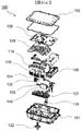
- FIG. 3A is an exploded perspective view of the DCDC converter device 100.
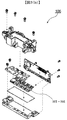
- FIG. 3B is an exploded perspective view of the high voltage circuit 106.
- FIG. 4A is an exploded perspective view showing the internal configuration of the DCDC converter device 100.
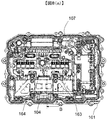
- FIG. 4B is a plan view showing the inside of the DCDC converter device 100.
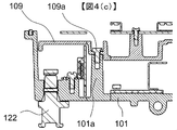
- FIG. 4C is a cross-sectional view of the AA cross section of FIG.
- FIG. 5 is a perspective view showing a low voltage substrate in the DCDC converter apparatus 100.
- the control circuit board 108 is mounted with a control circuit for controlling a switching element provided in the low voltage circuit or the high voltage circuit.
- the control circuit board 108 is fixed to a convex portion formed on the upper surface of the metal base plate 109 with a bolt or the like.
- the base plate 109 is bolted to a plurality of support portions protruding upward from the bottom surface portion of the case 101.
- the control circuit board 108 is disposed via the base plate 109 above the heat generating components (the main transformer 104, the inductor element 105, etc.) disposed on the bottom surface of the case.
- the circuit components of the DCDC converter device 100 are housed in a case 101 made of metal (for example, made of aluminum die casting).
- a case cover 102 is bolted to the opening of the case 101.
- the case 201 of the inverter device 200 is fixed to the bottom surface side of the case 101.
- a main transformer 104, an inductor element 105, a high voltage circuit 106 on which switching elements H1 to H4 are mounted, a low voltage circuit 107 on which switching elements SWA1 to SWA4 and SAWB1 to SWB4 are mounted, and the like are mounted on the bottom portion in the case. Is placed.
- An exploded perspective view of the high voltage circuit 106 is shown in FIG.
- the main transformer 104 corresponds to the transformer Tr
- the inductor element 105 corresponds to the reactors L1 and L2 of the current doubler.
- switching elements S1, S2, etc. of the active clamp circuit of FIG. 2 are also mounted.
- switching elements 170 to 177 are mounted on a metal substrate on which a pattern is formed.
- Bus bars 160, 161, 162, 163, 164, 190, and 191 made of a metal material are mounted on a metal substrate.
- the ferrite core 140 and the filter substrate 120 shown in FIG. 4A constitute an LC filter circuit installed to reduce the output noise of the DCDC converter device 100, and are mounted on the substrate of the low voltage circuit 107. Together with the smoothing capacitor 130, a ⁇ -type LC filter circuit is configured. Note that the circuit configuration aims to reduce output noise, and is not limited to a ⁇ -type LC filter circuit.
- the output terminal 122 shown in FIG. 4C functions as an output terminal when power is converted from the HV side to the LV side, but functions as an input terminal when power is converted from the LV side to the HV side. In the converter of this embodiment, power conversion in both the HV side and the LV side is possible, but there is also a converter that performs power conversion only in one direction.
- a shield wall 101a formed integrally with the case 101 is formed between the LC filter circuit and the low voltage circuit unit 107.
- the output bus bar 162 shown in FIG. 5 bypasses the shield wall 102 and electrically connects the low voltage circuit 107 and the ferrite core 140, the filter substrate 120, and the output terminal 122.
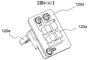
- FIG. 6 (a) and 6 (b) are perspective views showing the appearance of the filter substrate 120.
- FIG. 6 (a) and 6 (b) are perspective views showing the appearance of the filter substrate 120.
- a ceramic capacitor 120a is mounted on the substrate 120d and has a function of filtering noise.
- the holding member 120e is a member in which a filter output bus bar 120b for electrically connecting the capacitor 120a and the output terminal 122 and a GND bus bar 120c for electrically connecting the capacitor 120a and the case 101 are integrally molded. . Between the filter output bus bar 120b and the GND bus bar 120c, insulation is ensured by molding in a state where an insulator is sandwiched. The mounting tool 120e is held and fixed to the filter substrate 120d with screws.
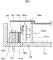
- FIG. 7 is a cross-sectional view illustrating the connection between the filter substrate 120 and the output terminal 122. Moreover, the arrow of a figure represents the direction through which the noise current which flows into a filter circuit flows.
- the filter output bus bar 120b and the GND bus bar 120c are arranged so as to face each other close to each other. Thereby, since the loop area formed by the filter output bus bar 120b, the filter substrate 120d, and the GND bus bar 120c can be reduced, the superposition of switching noise from the high voltage circuit 106 and the low voltage circuit 107 can be reduced.
- the output terminal 122 includes a metal part 122a and a mold part 122b.
- the mold part is fixed to the case 101 with screws (not shown).
- the filter output bus bar 120 b is fixed to the metal portion 122 a of the output terminal 122 with screws 150.
- the GND bus bar 120c is fixed to the case 101b with screws (not shown).
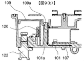
- case 101 and the base plate 109 are coupled and fixed by screws at the connecting portion 109a through the shield wall 101a, and the case 101 and the base plate 109 are electrically connected.
- the base plate 109 functions as a shield for shielding switching radiation noise from the switching element, and the noise current superimposed on the base plate 109 can be bypassed to the case 101 before flowing into the filter circuit unit 120. .
- the filter circuit is configured by electrically shielding the bus bar through which switching noise propagates and the filter circuit unit 120 with respect to noise superimposed on the base plate 109 due to switching between the high voltage circuit 106 and the low voltage circuit 107. It is possible to prevent a noise current from flowing to the unit 120, and thereby a sufficient filter effect of the filter circuit unit 120 can be obtained, so that noise can be reduced without reducing the filter effect.
- the high voltage circuit 106 and the low voltage circuit 107 are provided in the same casing. Since the filter circuit 120 can be mounted, it can be expected to reduce the size and the number of parts.
- FIG. 8A is a plan view showing the internal configuration of the DCDC converter device 100.
- FIG. 8B is a cross-sectional view of the BB cross section of FIG. 8A viewed from the arrow direction.
- the bus bar 160, 161, 163, 164 made of a metal material is mounted on the metal substrate in the low voltage circuit 107.
- the transformer 104 includes a bus bar 180 connected to the bus bar 163 or the bus bar 164.
- the transformer 104 is disposed on the bottom surface of the case 101 and on the side of the low voltage circuit 107.
- the bus bar 163 and the bus bar 164 rise from the low voltage circuit 107 and bend in the arrangement direction of the transformer 104.
- the low voltage circuit 107 and the transformer 104 are electrically connected by a bus bar 163 or a junction of the bus bar 164 and the bus bar 180.
- the bus bar 163 or the joint 181 between the bus bar 164 and the bus bar 180 is formed in a state in which the end surface 183 of the bus bar 163 or the bus bar 164 and the end surface 182 of the bus bar 180 are laminated so as to face the base plate 109 as described above. In the case of connection, the facing area between the bus bar 163, the bus bar 164, and the bus bar 180 and the base plate 109 can be reduced.
- the parasitic capacitance existing between the bus bars 163 and 164 connected to the transformer 104 and the base plate 109 can be reduced. Accordingly, the high voltage circuit 106 and the low voltage circuit 107 are switched. It is possible to reduce the switching noise from being superimposed on the base plate 109.
- FIG. 9A is a plan view showing the internal configuration of the DCDC converter device 100.
- FIG. 9B is a cross-sectional view of the AA cross section of FIG. 9A viewed from the arrow direction.
- the connecting portion 109a is located in a space between the filter circuit 120 and the ground terminal 101c and is located near the outer wall of the case 101. With this arrangement, the noise current superimposed on the base plate 109 passes through the shield wall 101a and its connecting portion 109a as shown by the arrow in FIG. Bypass to terminal 101c.
- the noise current superimposed on the base plate 109 can be prevented from propagating to the filter circuit 120, and noise caused by switching of the high-voltage circuit side switching circuit unit 106 and the low-voltage side switching circuit unit 107 is externally transmitted from the external output terminal. Can be reduced.
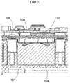
- FIG. 10 is a cross-sectional view of the DD cross section of FIG. 4B viewed from the arrow direction.
- the power conversion device in which the inverter and the converter are integrated has been described as an example, but a configuration in which the converter is a single unit is also possible.
Landscapes
- Engineering & Computer Science (AREA)
- Microelectronics & Electronic Packaging (AREA)
- Physics & Mathematics (AREA)
- Thermal Sciences (AREA)
- Power Engineering (AREA)
- Dc-Dc Converters (AREA)
Abstract
Description
上述したような接続の場合、バスバー163、バスバー164及びバスバー180と、ベース板109との対向面積を小さくすることができる。このことにより、トランス104と接続するバスバー163,164と,ベース板109との間に存在する寄生容量を小さくすることができ、よって、高電圧回路106と,低電圧回路107のスイッチングに起因するスイッチングノイズが,ベース板109に重畳することを低減することができる。
101:ケース
101a:シールド壁部、101b:保持部材の取付け部、101c:接地端子
13:入口配管、14:出口配管
200:インバータ装置、201:インバータケース
102:ケースカバー、
104:主トランス、104a、b:主トランスの端子
105:インダクタ素子
106:高電圧回路、107:低電圧回路、108:制御回路基板
109:ベース板、109a:接続部
120:フィルタ基板、120a:コンデンサ、120b:フィルタ出力バスバー、
120c:GNDバスバー、120d:基板、120e:保持部材
160、161、162、163、164、190、191:低電圧基板上のバスバー 140:フェライトコア
122:出力端子、122a:出力端子の金属部、122b:出力端子のモールド
110:金属板
H1~H4:スイッチング素子
Claims (5)
- トランスと、
前記トランスと高電圧側回路部との間に電気的に配置された高電圧側スイッチング回路部と、
前記トランスと低電圧側回路部との間に電気的に配置された低電圧側スイッチング回路部と、
前記低電圧側スイッチング回路部と前記低電圧側スイッチング回路部との間に電気的に配置されたノイズフィルタ回路部と、
前記トランスと前記高電圧側スイッチング回路部と前記低電圧側スイッチング回路部と前記ノイズフィルタ回路部とを収納する金属製のケースと、
前記低電圧側スイッチング回路部を駆動する駆動回路を有する駆動回路基板と、
前記駆動回路基板を搭載する金属製のベース板と、を備え、
前記ケースは、当該ケースと接続される金属製の隔壁を有し、
前記隔壁は、前記低電圧側スイッチング回路部と前記ノイズフィルタ回路部との間に配置され、
前記隔壁は、前記ベース板と接続されるDCDCコンバータ。 - 請求項1に記載されたDCDCコンバータであって、
前記ベース板は、前記低電圧側スイッチング回路部を挟んで前記ケースの底面と対向する位置に配置されるDCDCコンバータ。 - 請求項1又は2に記載されたいずれかのDCDCコンバータであって、
前記低電圧側スイッチング回路部は、第一バスバーを有し、
前記トランスは、第二バスバーを有し、前記低電圧側スイッチング回路部は、前記ケースの底面に配置され、
前記トランスは、前記ケースの底面であって前記低電圧側スイッチング回路部の側部に配置され、
前記第一バスバーは、前記低電圧側スイッチング回路部から立ち上がるとともに前記トランスの配置方向に向かって屈曲し、
前記低電圧側スイッチング回路部と前記トランスは、前記第一バスバーと前記第二バスバーの接合により電気的に接続され、
前記第一バスバーと前記第二バスバーの接合部は、前記第一バスバーの端側面と前記第二バスバーの端側面が前記ベース板に対向するように積層した状態で形成されるDCDCコンバータ。 - 請求項1ないし3に記載されたいずれかのDCDCコンバータであって、
前記ケースは、グラウンドに接地するための接地端子を有し、
前記隔壁と前記ベース板との接続部は、前記ノイズフィルタ回路部と前記接地端子との間の空間に配置されるDCDCコンバータ。 - 請求項1ないし4に記載されたいずれかのDCDCコンバータであって、
前記トランスを前記ケースの底面の方向に向かって押しつける金属製の押さえ板を備え、
前記押さえ板は、前記ベース板と前記トランスとの間の空間に配置されるDCDCコンバータ。
Priority Applications (3)
| Application Number | Priority Date | Filing Date | Title |
|---|---|---|---|
| US14/419,067 US9425695B2 (en) | 2012-08-03 | 2013-06-28 | DC-DC converter |
| DE112013003854.4T DE112013003854B4 (de) | 2012-08-03 | 2013-06-28 | Gleichstrom/Gleichstrom-Umsetzer |
| CN201380041223.6A CN104541442B (zh) | 2012-08-03 | 2013-06-28 | Dcdc转换器 |
Applications Claiming Priority (2)
| Application Number | Priority Date | Filing Date | Title |
|---|---|---|---|
| JP2012-172468 | 2012-08-03 | ||
| JP2012172468A JP6012330B2 (ja) | 2012-08-03 | 2012-08-03 | Dcdcコンバータ |
Publications (1)
| Publication Number | Publication Date |
|---|---|
| WO2014021035A1 true WO2014021035A1 (ja) | 2014-02-06 |
Family
ID=50027725
Family Applications (1)
| Application Number | Title | Priority Date | Filing Date |
|---|---|---|---|
| PCT/JP2013/067763 Ceased WO2014021035A1 (ja) | 2012-08-03 | 2013-06-28 | Dcdcコンバータ |
Country Status (5)
| Country | Link |
|---|---|
| US (1) | US9425695B2 (ja) |
| JP (1) | JP6012330B2 (ja) |
| CN (1) | CN104541442B (ja) |
| DE (1) | DE112013003854B4 (ja) |
| WO (1) | WO2014021035A1 (ja) |
Cited By (1)
| Publication number | Priority date | Publication date | Assignee | Title |
|---|---|---|---|---|
| WO2014173790A1 (de) * | 2013-04-26 | 2014-10-30 | Conti Temic Microelectronic Gmbh | Gehäuse, schaltungsanordnung, antriebsanordnung sowie verfahren zur herstellung der schaltungsanordnung |
Families Citing this family (18)
| Publication number | Priority date | Publication date | Assignee | Title |
|---|---|---|---|---|
| JP5504219B2 (ja) * | 2011-07-27 | 2014-05-28 | 日立オートモティブシステムズ株式会社 | 電力変換装置 |
| JP5855899B2 (ja) * | 2011-10-27 | 2016-02-09 | 日立オートモティブシステムズ株式会社 | Dc−dcコンバータ及び電力変換装置 |
| JP6101484B2 (ja) * | 2012-12-28 | 2017-03-22 | 日立オートモティブシステムズ株式会社 | Dc−dcコンバータ |
| US9866127B2 (en) | 2014-03-03 | 2018-01-09 | Hitachi Automotive Systems, Ltd. | Electrical power converting device |
| JP6213356B2 (ja) * | 2014-04-08 | 2017-10-18 | 株式会社デンソー | 電源装置 |
| JP6460477B2 (ja) * | 2015-04-03 | 2019-01-30 | オムロンオートモーティブエレクトロニクス株式会社 | 電子機器 |
| US10097096B2 (en) | 2016-05-04 | 2018-10-09 | Toyota Motor Engineering & Manufacturing North America, Inc. | Packaging of a power conversion circuit |
| DE102016119293A1 (de) * | 2016-10-11 | 2018-04-12 | HELLA GmbH & Co. KGaA | Elektronik, insbesondere Leistungselektronik und System |
| DE102017111396B4 (de) * | 2017-05-24 | 2020-08-06 | Hanon Systems | Anordnung zur aktiven Unterdrückung von Störsignalen |
| JP6466005B1 (ja) * | 2018-02-01 | 2019-02-06 | 三菱電機株式会社 | 電力変換装置 |
| KR102706102B1 (ko) | 2018-10-19 | 2024-09-13 | 한온시스템 주식회사 | 인버터 모듈 및 이를 포함하는 전동압축기 |
| WO2020080869A1 (ko) * | 2018-10-19 | 2020-04-23 | 한온시스템 주식회사 | 인버터 모듈 및 이를 포함하는 전동압축기 |
| DE102018129415B4 (de) * | 2018-11-22 | 2024-07-04 | Dr. Ing. H.C. F. Porsche Aktiengesellschaft | Ladevorrichtung für ein Fahrzeug und Fahrzeug mit einer Ladevorrichtung |
| US12191722B2 (en) * | 2019-05-31 | 2025-01-07 | MagniX USA, Inc. | High-torque electric motor assembly |
| CN112928909B (zh) * | 2019-12-06 | 2023-03-07 | 重庆大及电子科技有限公司 | 一种emi滤波装置 |
| JP7515588B2 (ja) | 2020-07-03 | 2024-07-12 | 三菱電機株式会社 | 電力変換装置 |
| JP7098025B1 (ja) * | 2021-06-09 | 2022-07-08 | 三菱電機株式会社 | 電力変換装置 |
| CN120439775A (zh) * | 2024-02-08 | 2025-08-08 | 华为数字能源技术有限公司 | 多合一供电装置、多合一动力总成及电动车 |
Citations (4)
| Publication number | Priority date | Publication date | Assignee | Title |
|---|---|---|---|---|
| JP2000324839A (ja) * | 1999-04-30 | 2000-11-24 | Denso Corp | 降圧型dc−dcコンバータ装置 |
| JP2009284701A (ja) * | 2008-05-23 | 2009-12-03 | Sharp Corp | スイッチング電源装置 |
| JP2011004520A (ja) * | 2009-06-18 | 2011-01-06 | Honda Motor Co Ltd | 電力変換装置 |
| WO2011125781A1 (ja) * | 2010-04-01 | 2011-10-13 | 日立オートモティブシステムズ株式会社 | 電力変換装置 |
Family Cites Families (9)
| Publication number | Priority date | Publication date | Assignee | Title |
|---|---|---|---|---|
| CN1617663A (zh) * | 2003-11-14 | 2005-05-18 | 乐金电子(沈阳)有限公司 | 利用屏蔽板的噪声滤波部电子波屏蔽结构 |
| JP4693781B2 (ja) * | 2004-11-17 | 2011-06-01 | シャープ株式会社 | アクティブマトリクス基板及び表示装置 |
| JP2006180578A (ja) * | 2004-12-20 | 2006-07-06 | Nippon Soken Inc | 電力変換装置 |
| JP2008125283A (ja) * | 2006-11-14 | 2008-05-29 | Fuji Electric Holdings Co Ltd | 電力変換装置 |
| JP4988665B2 (ja) | 2008-08-06 | 2012-08-01 | 日立オートモティブシステムズ株式会社 | 半導体装置および半導体装置を用いた電力変換装置 |
| JP5110027B2 (ja) * | 2009-04-03 | 2012-12-26 | 株式会社デンソー | 高周波シールドケース |
| US8169780B2 (en) | 2009-06-18 | 2012-05-01 | Honda Motor Co., Ltd. | Power conversion device |
| JP5099379B2 (ja) * | 2009-12-28 | 2012-12-19 | Tdk株式会社 | ベースプレート構造および電源装置 |
| JP5743851B2 (ja) | 2011-10-31 | 2015-07-01 | 日立オートモティブシステムズ株式会社 | 電子装置 |
-
2012
- 2012-08-03 JP JP2012172468A patent/JP6012330B2/ja active Active
-
2013
- 2013-06-28 CN CN201380041223.6A patent/CN104541442B/zh active Active
- 2013-06-28 DE DE112013003854.4T patent/DE112013003854B4/de active Active
- 2013-06-28 WO PCT/JP2013/067763 patent/WO2014021035A1/ja not_active Ceased
- 2013-06-28 US US14/419,067 patent/US9425695B2/en active Active
Patent Citations (4)
| Publication number | Priority date | Publication date | Assignee | Title |
|---|---|---|---|---|
| JP2000324839A (ja) * | 1999-04-30 | 2000-11-24 | Denso Corp | 降圧型dc−dcコンバータ装置 |
| JP2009284701A (ja) * | 2008-05-23 | 2009-12-03 | Sharp Corp | スイッチング電源装置 |
| JP2011004520A (ja) * | 2009-06-18 | 2011-01-06 | Honda Motor Co Ltd | 電力変換装置 |
| WO2011125781A1 (ja) * | 2010-04-01 | 2011-10-13 | 日立オートモティブシステムズ株式会社 | 電力変換装置 |
Cited By (3)
| Publication number | Priority date | Publication date | Assignee | Title |
|---|---|---|---|---|
| WO2014173790A1 (de) * | 2013-04-26 | 2014-10-30 | Conti Temic Microelectronic Gmbh | Gehäuse, schaltungsanordnung, antriebsanordnung sowie verfahren zur herstellung der schaltungsanordnung |
| JP2016518717A (ja) * | 2013-04-26 | 2016-06-23 | コンティ テミック マイクロエレクトロニック ゲゼルシャフト ミット ベシュレンクテル ハフツングConti Temic microelectronic GmbH | ハウジング、回路装置、駆動装置及び回路装置を製造する方法 |
| US10390467B2 (en) | 2013-04-26 | 2019-08-20 | Conti Temic Microelectronic Gmbh | Housing, circuit arrangement, drive arrangement and method for producing the circuit arrangement |
Also Published As
| Publication number | Publication date |
|---|---|
| JP2014033531A (ja) | 2014-02-20 |
| CN104541442B (zh) | 2017-03-15 |
| US9425695B2 (en) | 2016-08-23 |
| US20150194898A1 (en) | 2015-07-09 |
| DE112013003854B4 (de) | 2021-11-25 |
| JP6012330B2 (ja) | 2016-10-25 |
| DE112013003854T5 (de) | 2015-04-23 |
| CN104541442A (zh) | 2015-04-22 |
Similar Documents
| Publication | Publication Date | Title |
|---|---|---|
| JP6012330B2 (ja) | Dcdcコンバータ | |
| JP5743851B2 (ja) | 電子装置 | |
| JP5738794B2 (ja) | 電力変換装置 | |
| JP7060024B2 (ja) | 電子回路装置 | |
| US9713292B2 (en) | DC-DC converter and power conversion apparatus | |
| JP6175556B2 (ja) | 電力変換装置 | |
| JP6104347B1 (ja) | 電力変換装置 | |
| JP7152296B2 (ja) | 電力変換装置、及び高電圧ノイズフィルタ | |
| JP6101484B2 (ja) | Dc−dcコンバータ | |
| WO2013015106A1 (ja) | 電力変換装置 | |
| JP6218150B2 (ja) | 電力変換装置 | |
| WO2013065472A1 (ja) | 一体型電力変換装置及びそれに用いられるdcdcコンバータ装置 | |
| KR20150096455A (ko) | 냉각기를 구비한 리액터 | |
| JP2013094023A (ja) | 電力変換装置 | |
| JP2013027077A (ja) | 電力変換装置 | |
| WO2015053141A1 (ja) | Dc-dcコンバータ装置 | |
| JP6055868B2 (ja) | 電力変換装置 | |
| JP5601535B2 (ja) | 電源装置 | |
| JP2021151073A (ja) | 電力変換装置 | |
| JP6186439B2 (ja) | Dc−dcコンバータ装置 | |
| JP7843732B2 (ja) | 電力変換装置 |
Legal Events
| Date | Code | Title | Description |
|---|---|---|---|
| 121 | Ep: the epo has been informed by wipo that ep was designated in this application |
Ref document number: 13826296 Country of ref document: EP Kind code of ref document: A1 |
|
| WWE | Wipo information: entry into national phase |
Ref document number: 14419067 Country of ref document: US |
|
| WWE | Wipo information: entry into national phase |
Ref document number: 1120130038544 Country of ref document: DE Ref document number: 112013003854 Country of ref document: DE |
|
| 122 | Ep: pct application non-entry in european phase |
Ref document number: 13826296 Country of ref document: EP Kind code of ref document: A1 |