WO2014017652A1 - 照明装置 - Google Patents
照明装置 Download PDFInfo
- Publication number
- WO2014017652A1 WO2014017652A1 PCT/JP2013/070379 JP2013070379W WO2014017652A1 WO 2014017652 A1 WO2014017652 A1 WO 2014017652A1 JP 2013070379 W JP2013070379 W JP 2013070379W WO 2014017652 A1 WO2014017652 A1 WO 2014017652A1
- Authority
- WO
- WIPO (PCT)
- Prior art keywords
- lens
- light
- light source
- optical
- light emitting
- Prior art date
- Legal status (The legal status is an assumption and is not a legal conclusion. Google has not performed a legal analysis and makes no representation as to the accuracy of the status listed.)
- Ceased
Links
Images




















Classifications
-
- F—MECHANICAL ENGINEERING; LIGHTING; HEATING; WEAPONS; BLASTING
- F21—LIGHTING
- F21V—FUNCTIONAL FEATURES OR DETAILS OF LIGHTING DEVICES OR SYSTEMS THEREOF; STRUCTURAL COMBINATIONS OF LIGHTING DEVICES WITH OTHER ARTICLES, NOT OTHERWISE PROVIDED FOR
- F21V5/00—Refractors for light sources
- F21V5/008—Combination of two or more successive refractors along an optical axis
-
- F—MECHANICAL ENGINEERING; LIGHTING; HEATING; WEAPONS; BLASTING
- F21—LIGHTING
- F21K—NON-ELECTRIC LIGHT SOURCES USING LUMINESCENCE; LIGHT SOURCES USING ELECTROCHEMILUMINESCENCE; LIGHT SOURCES USING CHARGES OF COMBUSTIBLE MATERIAL; LIGHT SOURCES USING SEMICONDUCTOR DEVICES AS LIGHT-GENERATING ELEMENTS; LIGHT SOURCES NOT OTHERWISE PROVIDED FOR
- F21K9/00—Light sources using semiconductor devices as light-generating elements, e.g. using light-emitting diodes [LED] or lasers
- F21K9/60—Optical arrangements integrated in the light source, e.g. for improving the colour rendering index or the light extraction
-
- F—MECHANICAL ENGINEERING; LIGHTING; HEATING; WEAPONS; BLASTING
- F21—LIGHTING
- F21V—FUNCTIONAL FEATURES OR DETAILS OF LIGHTING DEVICES OR SYSTEMS THEREOF; STRUCTURAL COMBINATIONS OF LIGHTING DEVICES WITH OTHER ARTICLES, NOT OTHERWISE PROVIDED FOR
- F21V5/00—Refractors for light sources
- F21V5/04—Refractors for light sources of lens shape
-
- G—PHYSICS
- G02—OPTICS
- G02B—OPTICAL ELEMENTS, SYSTEMS OR APPARATUS
- G02B19/00—Condensers, e.g. light collectors or similar non-imaging optics
- G02B19/0004—Condensers, e.g. light collectors or similar non-imaging optics characterised by the optical means employed
- G02B19/0009—Condensers, e.g. light collectors or similar non-imaging optics characterised by the optical means employed having refractive surfaces only
- G02B19/0014—Condensers, e.g. light collectors or similar non-imaging optics characterised by the optical means employed having refractive surfaces only at least one surface having optical power
-
- G—PHYSICS
- G02—OPTICS
- G02B—OPTICAL ELEMENTS, SYSTEMS OR APPARATUS
- G02B19/00—Condensers, e.g. light collectors or similar non-imaging optics
- G02B19/0033—Condensers, e.g. light collectors or similar non-imaging optics characterised by the use
- G02B19/0047—Condensers, e.g. light collectors or similar non-imaging optics characterised by the use for use with a light source
- G02B19/0061—Condensers, e.g. light collectors or similar non-imaging optics characterised by the use for use with a light source the light source comprising a LED
-
- F—MECHANICAL ENGINEERING; LIGHTING; HEATING; WEAPONS; BLASTING
- F21—LIGHTING
- F21Y—INDEXING SCHEME ASSOCIATED WITH SUBCLASSES F21K, F21L, F21S and F21V, RELATING TO THE FORM OR THE KIND OF THE LIGHT SOURCES OR OF THE COLOUR OF THE LIGHT EMITTED
- F21Y2115/00—Light-generating elements of semiconductor light sources
- F21Y2115/10—Light-emitting diodes [LED]
Definitions
- the present invention relates to a lighting device including a surface light source.
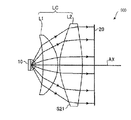
- an illumination device 900 shown in FIG. 62 is known as a general illumination device.
- the illumination device 900 has a collimating optical system LC including a meniscus lens L1 and an aspheric lens L2, and the LED light source 10 is disposed at the focal position of the optical system. .
- the light emitted from one point existing on the optical axis AX of the LED light source 10 is extracted as collimated light parallel to the optical axis AX as shown in FIG.
- the LED light source 10 is not a point light source but a surface light source, there is also light emitted from a place off the optical axis AX. Since the light emitted from a place off the optical axis AX is emitted in a direction different from the optical axis AX, the light is emitted to a place different from the light emitted from one point existing on the optical axis AX. For this reason, the problem that the illumination intensity uniformity in an irradiation surface cannot be obtained arises.
- the meniscus lens L1 and the LED light source 10 are separated from each other, there is a possibility that light emitted from the LED light source 10 at a large angle may not enter the meniscus lens L1.
- Patent Documents 1 and 2 disclose a light source that can use almost all of the light emitted from the LED light emitter.
- the light source described in Patent Document 1 includes an LED light emitter, an internal lens that encloses the LED light emitter, and a meniscus lens that covers these.
- the light source described in Patent Literature 2 includes an LED light emitter and a meniscus lens that covers the LED light emitter with a gap. In these light sources, the virtual image Vl 1 formed by the inner surface of the meniscus lens is generated on the outer side (the light emitting surface side of the lens) further than the LED light emitter.
- the present invention has been made to solve the above-described problems, and an object of the present invention is to provide an illuminating device with high uniformity of irradiation light intensity.
- An illuminating device includes a surface light source having a light exit surface, a first lens having a first focal point and disposed on the light exit surface side of the surface light source, and a second focus. And a second lens disposed on the light exit surface side of the first lens, so that the first virtual image is formed by the first lens and the second virtual image is formed by the second lens.
- the second focal point is located on a side opposite to the surface light source with respect to a position away from the principal point of the second lens by a predetermined focal distance f ′, and the principal point of the second lens and the point
- the distance from the position of the first virtual image is l ′
- the effective diameter of the second lens is D.
- the first virtual image formed by the first lens is located closer to the surface light source than the focal point of the second lens.
- the first virtual image is formed between the first focal point and the first lens
- the second virtual image is formed between the second focal point and the second lens. It is formed.
- the first virtual image and the second virtual image are formed between a synthetic focus of the first lens and the second lens and the first lens.
- a second optical system is further provided on the light exit side of the first optical system including the first lens and the second lens.
- the second optical system includes a concave lens that is closest to the first optical system and a convex lens that is next to the first optical system next to the concave lens.
- the light emitting surface of the first lens and the light incident surface of the second lens are joined.
- the first lens and the second lens are integrally formed of resin.
- the lens surface of the first lens facing the surface light source is a concave curved surface
- the distance from the light emitting surface of the surface light source on the optical axis to the concave curved surface of the first lens is d.
- the range width h of the position where the light emitting surface can be arranged is represented by h ⁇ 2 ⁇ (d (2R ⁇ d)).
- the distance from the principal point of the optical lens unit including the first lens and the second lens to the light emitting surface is a, and the distance from the principal point of the optical lens unit to the focal position is f.
- a ⁇ f / 2 is satisfied.
- the surface light source includes a plurality of light emitting elements that are spaced apart from each other.
- the first lens and the second lens are made of a material having an Abbe number of 54 or more.
- the first lens and the second lens are made of a heat resistant material.
- At least one of the first lens and the second lens is an achromatic lens.
- the achromatic lens is composed of a concave lens and a convex lens that is in close contact with the concave lens, and a junction interface at a central portion of the concave lens and the convex lens is a flat surface.
- the light source further includes a light diffusion layer provided between the surface light source and the first lens.
- the light diffusion layer has a haze value of 5% to 50%.
- the surface light source includes a plurality of light emitting elements arranged at a pitch P and a phosphor disposed so as to overlap the plurality of light emitting elements, the edge of the phosphor, and the phosphor When the distance from the edge of the light emitting element disposed at the position closest to the edge of A is A, A ⁇ P is satisfied.
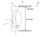
- the apparatus further includes a hood that is disposed on the light emission side of the second lens and is provided so as to block only a part of the light emitted from the second lens.
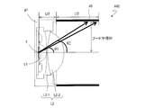
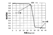
- the distance Lf1 + Lf2 from the position of the light emitting surface of the surface light source on the optical axis to the position of the tip of the hood is the minimum angle at which the slope of the angle-relative illuminance graph is smaller than ⁇ 0.1.
- Is ⁇ 1 the emission angle at which the stray light ratio expressed by the luminous flux in the stray light region / (the luminous flux in the irradiation region + the luminous flux in the stray light region) is 1% or less is ⁇ 2, and the radius of the hood is Rf. It satisfies tan ⁇ 2 ⁇ Lf1 + Lf2 ⁇ Rf / tan ⁇ 1.
- an antireflection layer is provided on at least one of the light emitting surface and the light incident surface of the first lens and the light emitting surface and the light incident surface of the second lens.
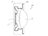
- a light absorption layer is provided on at least one edge of the first lens and the second lens.
- a housing having a space for housing the surface light source, the first lens, and the second lens is further provided, and a light absorption layer is provided in at least a part of the housing portion defining the outside of the housing space. It has been.
- the lighting device described in any of the above is used as a headlight of an automobile.
- the region inside the intersection of the tangent of the point where the relative illuminance is 0.10 and the axis indicating the irradiation angle is irradiated.
- the stray light ratio represented by the luminous flux in the stray light area / (the luminous flux in the irradiation area + the luminous flux in the stray light area) is 3% or less, where the area outside the irradiation area is the stray light area.
- the light emitted from the center of the light emitting unit existing on the optical axis of the optical lens unit and the light emitted from a position off the center of the light emitting unit are substantially equal.
- the light can be emitted from the optical lens unit with an angular distribution. Therefore, since the light emitted from the center of the light emitting unit and the light emitted from a position off the center of the light emitting unit can be irradiated in the same manner over the entire predetermined irradiation region, the uniformity of the irradiation region is drastically improved. It becomes possible to improve.
- the light emitted from the center of the light emitting unit and the light emitted from a position deviating from the center of the light emitting unit can be emitted from the optical lens unit with a substantially equal angular distribution, and thus are not emitted to the optical lens unit. Light can be almost eliminated, and as a result, high light utilization efficiency can be realized.
- the focal points of the optical lenses constituting the optical lens unit are synthesized.
- the combined focal position may be present on the opposite side of the surface of the virtual image that faces the light emitting unit with respect to the virtual images generated by the optical lenses.
- the combined focal position obtained by combining the focal points of the optical lenses constituting the optical lens unit is opposed to the light emitting units of all the virtual images with respect to the virtual images generated by the optical lenses.
- a virtual image by each lens can be generated at a position closer to the light emitting portion.
- the angle of light emitted from the optical lens unit can be expanded, so that the uniformity of a wider irradiation area can be dramatically improved.
- a second optical lens unit may be provided on the light exit side of the first optical lens unit.
- the emission angle of the light emitted from the first optical lens unit can be changed by the second optical lens unit. That is, by adjusting the optical characteristics of the second optical lens unit, it is possible to narrow or widen the emission angle of the light emitted from the first optical lens unit.
- the second optical lens unit may be formed of a concave lens for a lens closest to the first optical lens unit and a convex lens for a lens next closest to the first optical lens unit.
- the aberration generated in each lens can be corrected by the combination of the concave lens and the convex lens, the characteristics of the light emitted from the first optical lens unit can be prevented from being destroyed.
- the emission angle of the light emitted from the first optical lens unit can be adjusted, and almost all the light emitted from the light emitting unit can be used, realizing high light utilization efficiency.
- each lens interface may be integrally formed.
- each lens constituting the optical lens unit since a part of each lens constituting the optical lens unit is integrally formed, the light emitting surface of the light emitting unit and the optical lens unit can be easily aligned.
- the light emitting part and the optical lens part can be easily fixed.
- Integral molding with resin and adhesion with an adhesive can be considered as an integral method of forming the two lenses.
- the two lenses may be integrally molded with resin.
- the two lenses are integrally formed of resin, the number of moldings when forming the optical lens portion can be reduced from two times (in the case of two lenses) to one time. Reduction can be achieved.
- a first optical lens having a lens surface closest to the light emitting unit as a concave surface recessed toward the light emitting unit, and a first on the optical axis from the light emitting surface of the light emitting unit.
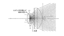
- the radius of curvature of the inner lens of the first optical lens is R
- the arrangement range of the light emitting part on the optical axis is h, h ⁇ 2 ⁇ (d (2R ⁇ d )).
- the virtual image position is always made optical by making the distance a from the principal point of the optical lens part to the light emitting surface of the light emitting part shorter than half the distance f from the principal point of the optical lens part to the focal position.
- the optical lens unit can be relatively closer than the focal position of the lens unit.
- the light emitting unit may include a plurality of light emitters.
- a plurality of light emitters are arranged on the light emitting surface of the light emitting unit. Even if there is a variation in the amount of light emitted from each light emitter, the irradiation surface should absorb these variations. Light is irradiated. That is, since any light emitter emits light to the same irradiation region, even if there is a variation in the light emission amount of the light emitter, this variation is absorbed.
- a uniform illuminance distribution can be realized.
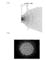
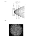
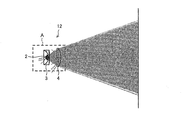
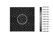
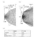
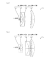
- FIG. 2 It is a schematic block diagram of the illuminating device which concerns on embodiment of this invention. It is a schematic block diagram of the illuminating device which concerns on embodiment of this invention. It is a figure which shows the light beam behavior in the illuminating device shown in FIG. (A) shows schematic structure of the illuminating device shown in FIG. 2, (b) is a figure which shows schematic structure of the illuminating device of a comparative example. (A) is a figure which shows the light beam behavior of the illuminating device shown to Fig.4 (a), (b) is a figure which shows the light beam behavior of the illuminating device shown in FIG.3 (b).
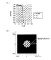
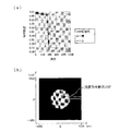
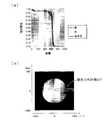
- FIG. 1 shows an example in which a plurality of minute light emitting surfaces are arranged, (b) shows an example in which a part of the minute light emitting surface is dark, and (c) shows an irradiation intensity distribution in FIG. FIG.
- A) shows the two-dimensional illuminance distribution on the evaluation surface a shown in FIG.
- FIG. 10 shows the two-dimensional illuminance distribution on the evaluation surface b shown in FIG.
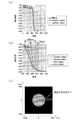
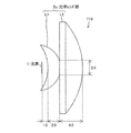
- A) shows the optical lens conditions for actually manufacturing the illumination device shown in FIG. 1, and (b) is a diagram showing the illuminance state in the irradiation region obtained when the illumination device shown in FIG. 1 is actually manufactured. is there.
- A) shows the optical lens conditions for actually producing the illumination device shown in FIG. 2, and (b) is a diagram showing the illuminance state in the irradiation region obtained when the illumination device shown in FIG. 2 is actually produced. is there.
- It is a schematic block diagram of the illuminating device which concerns on other embodiment of this invention. It is an enlarged view of the principal part A of the illuminating device shown in FIG.
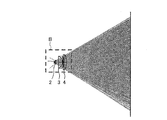
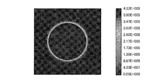
- FIG. It is a figure which shows the irradiation intensity distribution in the illuminating device shown in FIG. It is a schematic block diagram of the illuminating device which concerns on other embodiment of this invention. It is an enlarged view of the principal part B of the illuminating device shown in FIG. It is a figure which shows the irradiation intensity distribution in the illuminating device shown in FIG. It is a schematic block diagram of the illuminating device which concerns on other embodiment of this invention. It is a schematic block diagram of the illuminating device which concerns on other embodiment of this invention. It is a figure which shows the relationship between an illuminating device and an evaluation surface. It is a figure which shows the irradiation intensity distribution in the evaluation surface shown in FIG.
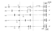
- FIG. 5 is a diagram showing the relationship between the focal points of the first lens and the second lens and the position of a virtual image formed by each lens, and (a) to (e) show different arrangement relationships. It is a figure which shows the illumination intensity nonuniformity which arises on the light-projection surface of a surface light source. It is a figure which shows the positional relationship of the reference
- (A) is a figure for demonstrating a pan focus state
- (b) is a figure for demonstrating the case where it applies to an illuminating device. It is a figure for demonstrating that the position of the reference
- FIG. 4 is a diagram showing a light source provided in the illumination device of Embodiment 4-2, (a) and (b) showing different forms, and (c) for explaining the arrangement of the light diffusion layers provided in this embodiment.
- FIG. (A) is a diagram showing a light source of a lighting device of a comparative example
- (b) to (e) are diagrams showing a light source of the lighting device of Embodiment 4-3.
- FIG. 43 shows distribution of BR difference in the illuminating device shown in FIG.43 (c).
- FIG. 56 (a) shows arrangement
- (b) is illumination light.
- the arrangement of each lens when the irradiation angle is a wide angle is shown. It is a figure for demonstrating the optical characteristic of the illuminating device shown to Fig.57 (a), (a) shows illuminance distribution when light bulb color, blue, and red of 3 types are included in irradiation light. , (B) shows a color chart. It is a figure for demonstrating the optical characteristic of the illuminating device shown in FIG.57 (b), (a) shows illuminance distribution when light bulb color, blue, and red of 3 types are included in irradiation light.
- FIG. 61 is a diagram for explaining optical characteristics of the illumination device shown in FIG. 60, where (a) shows an illuminance distribution when the light emitted includes three types of light of a light bulb color, blue, and red; ) Shows a color chart. It is sectional drawing which shows the conventional illuminating device.
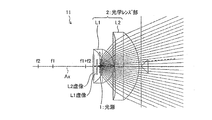
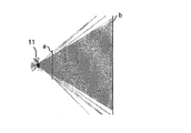
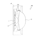
- ⁇ Embodiment 1> 1 and 2 are diagrams showing a schematic configuration of the illumination device 11 according to the present embodiment.
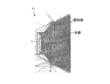
- FIG. 3 is a diagram showing a light irradiation state in the illumination device 11 shown in FIG.
- the illuminating device 11 includes a light source (light emitting unit) 1 and an optical lens unit 2 disposed on an optical axis AX on the light emitting surface side that is the light extraction side of the light source 1.
- the light emitted from the light source 1 is irradiated through the optical lens unit 2.
- the light source 1 includes an LED light emitter that is a surface light emitter that performs surface light emission. In addition, if it is a surface light-emitting body which performs surface light emission, it will not be limited to a LED light-emitting body.
- the optical lens unit 2 includes two optical lenses L1 and L2, and in order from the side closer to the light source 1, an optical lens L1 (sometimes referred to as a first lens L1) and an optical lens L2 (second lens).
- the lens L2 may be called).
- the optical lenses L1 and L2 are arranged so that their centers pass through the optical axis AX.
- the optical lens L1 has at least a diameter larger than the maximum width of the light emitting surface of the light source 1, and is composed of an optical lens having a concave surface on the light source 1 side.
- the optical lens L2 has a diameter larger than the maximum diameter of the optical lens L1, which is at least the first optical lens, and includes a convex lens on the light exit surface side.
- the focal position of the optical lens L1 is f1 (sometimes referred to as a focal point F1), and a virtual image generated when light from the light source 1 passes through the optical lens L1 is an L1 virtual image (sometimes called a virtual image I1).
- the focal position of the optical lens L2 is f2 (sometimes referred to as a focal point F2), and a virtual image generated when light from the L1 virtual image generated by the optical lens L1 passes through the optical lens L2 is an L2 virtual image (virtual image I2). May be called).
- the combined focal position of the optical lenses L1 and L2 is defined as f1 + f2 (sometimes referred to as a combined focal point F (1 + 2)).
- the focal points f1 and f2 of the optical lenses L1 and L2 constituting the optical lens unit 2 correspond to the virtual images (L1 virtual image and L2 virtual image) generated by the optical lenses L1 and L2, respectively.
- the optical lens unit 2 is designed so that each virtual image (L1 virtual image, L2 virtual image) exists on the side opposite to the surface facing the light source 1.
- a first virtual image I1 is formed between the focal point f1 and the lens L1
- a second virtual image I2 is formed between the focal point f2 and the lens L2.
- the illumination device 11 includes a light source (light emitting unit) 1 and an optical lens unit disposed on the optical axis AX on the light emitting surface side of the light source 1. 2, and the light emitted from the light source 1 is irradiated through the optical lens unit 2.
- the light source 1 includes an LED light emitter that is a surface light emitter that performs surface light emission. In addition, if it is a surface light-emitting body which performs surface light emission, it will not be limited to a LED light-emitting body.
- the optical lens unit 2 includes two optical lenses L1 (first optical lenses) and L2, and has a structure in which the optical lens L1 and the optical lens L2 are arranged in order from the side closer to the light source 1.
- the optical lenses L1 and L2 are arranged so that their centers pass through the optical axis AX.
- the optical lens L1 has a diameter larger than at least the maximum width of the light emitting surface of the light source 1, and is composed of an optical lens having a concave surface on the light source 1 side.
- the optical lens L2 has a diameter larger than the maximum diameter of the optical lens L1, which is at least the first optical lens, and is formed of a convex lens on the light exit surface side.
- the focal position of the optical lens L1 is f1, and the virtual image generated when the light from the light source 1 passes through the optical lens L1 is L1 virtual image.
- the focal position of the optical lens L2 is f2, and a virtual image generated when light from the L1 virtual image generated by the optical lens L1 passes through the optical lens L2 is referred to as an L2 virtual image. Further, the combined focal position of the optical lenses L1 and L2 is set to f1 + f2.
- the combined focal position f1 + f2 obtained by combining the focal points f1 and f2 of the optical lenses L1 and L2 constituting the optical lens unit 2 is a virtual image (L1 virtual image
- the optical lens unit 2 is designed so as to exist on the opposite side of the surface facing the light source 1 of all the virtual images (L1 virtual image, L2 virtual image) with respect to the L2 virtual image).
- an L1 virtual image and an L2 virtual image are formed between the combined focal position f1 + f2 of the lens L1 and the lens L2 and the lens L1.
- the illuminating device 11 in which the focal positions of the optical lenses L1 and L2 and the virtual images generated after passing through the optical lenses L1 and L2 have a relationship as shown in FIG. 2, as shown in FIG. It is possible to guide all the light beams to the optical lens unit 2 and efficiently irradiate the irradiated surface with light. That is, according to the illumination device 11 having the above-described configuration, it is possible to achieve both high light utilization efficiency and improvement in uniformity of the irradiated surface.
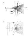
- FIG. 4A shows the focal positions of the optical lenses L1 and L2, and the L1 virtual image and the L2 virtual image generated after passing through the optical lenses L1 and L2 in the lens configuration (two-lens configuration) of the illumination device 11 of FIG.
- FIG. 4B shows a model diagram of the focal positions of the optical lenses L1 and L2 and the L1 virtual image and the L2 virtual image generated after passing through the optical lenses L1 and L2 in another embodiment. ing.
- the focal positions f1 and f2 of the optical lenses L1 and L2 and the combined focal position f1 + f2 are generated by the optical lenses L1 and L2 with respect to the position of the light source.
- the optical lens unit 2 is designed so that it exists on the opposite side of the light source side from the position of the virtual image (L1 virtual image, L2 virtual image).
- the virtual image (L1 virtual image, L2 virtual image) at each of the optical lenses L1 and L2 is formed relatively near the light source.
- the light after passing through a plurality of lenses (optical lenses L1 and L2) can be regarded as light emitted from a virtual image (L2 virtual image in FIG. 4A) generated by the final lens, an L2 virtual image is generated near the light source. By doing so, an effect as shown in FIG. 5A can be expected.
- FIG. 5A shows light emitted from the center of the light source (thin line in FIG. 5A) and light emitted from the upper end of the light source in the lens configuration shown in FIG. 4A (in FIG. 5A).
- the center of the light source means a portion passing through the optical axis AX passing through the center of the optical lens unit 2.
- the light emitted from the center of the light source and the light emitted from the upper end of the light source are emitted from the optical lens unit 2 with substantially the same angular distribution.
- the lens configuration shown in FIG. 4A the light emitted from the center of the light source and the light emitted from the upper end of the light source can be irradiated in the same manner over the entire predetermined irradiation region. The uniformity of the area can be improved.
- the L2 virtual image is formed at a relatively distant position by the second optical lens L2, which is shown in FIG. Unlike the above embodiment, no L2 virtual image is arranged between the optical lens L2 and its focal position f2.
- the focal position f2 of the optical lens L2 is disposed at a location relatively close to the L1 virtual image.
- the L2 virtual image is generated at a location farther from the light source than the focal position f2 of the optical lens L2, and the result shown in FIG. 5B may be obtained.
- the L1 virtual image is formed at least on the light source side with respect to the focal position f2 of the optical lens L2, and the virtual image formed by the optical lens L1.
- the optical system is configured such that I1 and the focal position f2 of the optical lens L2 are separated from the light source 1 by a predetermined distance or more as will be described later, the illuminance uniformity in the irradiation region can be improved. .
- FIG. 5B shows the light emitted from the center of the light source when the L1 virtual image is formed in the vicinity of the light source when the lens configuration of FIG. 4B is adopted (in FIG. 5B).
- An example of a path between a thin line) and light emitted from the upper end of the light source (thick line in FIG. 5B) is shown.
- the light emitted from the center of the light source and the light emitted from the upper end of the light source are emitted from the optical lens L2 with different angular distributions. ing. With such characteristics, light emitted from different places of the light source irradiates different ranges, and there is a possibility that the uniformity of the irradiated area cannot be obtained.
- the focal positions f1 and f2 of the optical lenses L1 and L2 arranged on the light emitting surface side of the light source are set as the optical lenses L1 and L2.
- the L1 virtual image and the L2 virtual image to be formed are arranged farther rearward (in the opposite direction to the lens exit side). Thereby, the light source and the virtual image position can be relatively moved closer to the optical lenses L1 and L2.
- the light emitted from the center of the light source existing on the optical axis of the optical lens unit and the light emitted from a position deviating from the center of the light source are approximately equal in angular distribution with the optical lens unit 2.
- the light can be emitted to the optical lens L1.
- the light emitted from the center of the light source and the light emitted from a position outside the center of the light source can be irradiated in the same manner throughout the predetermined irradiation region, so that the illuminance uniformity in the irradiation region is improved. It becomes possible.
- the light emitted from the center of the light source and the light emitted from the position deviating from the center of the light source can be emitted to the optical lens unit with substantially the same angular distribution, and thus are not emitted to the optical lens unit 2.
- Light can be almost eliminated, and as a result, high light utilization efficiency can be realized.
- the focal positions f1, f2 and the combined focal position f1 + f2 of the optical lenses L1, L2 are all the virtual images (L1) for the virtual images (L1 virtual image, L2 virtual image) generated by the optical lenses L1, L2.
- L1 virtual image, L2 virtual image Virtual image, L2 virtual image
- L2 virtual image is present on the side opposite to the surface facing the light source 1, so that a virtual image by each lens can be generated at a position closer to the light emitting portion.
- the angle of light emitted from the optical lens unit can be expanded, so that the uniformity of a wider irradiation area can be dramatically improved.
- the position of the virtual image I2 formed by the lens L2 is not necessarily formed in the vicinity of the light source 1, and the virtual image I2 may be formed at a position relatively far from the light source.
- the lighting device emits light at a relatively narrow angle.
- the focal point F2 of the second lens L2 is provided at a position separated from the L1 virtual image I1 or the light source by a predetermined distance or more. It is suitable for improving the uniformity.
- 27A to 27E show various positional relationships between the positions of the focal points F1 and F2 of the lenses L1 and L2 and the virtual images I1 and I2.
- the light source 1 is disposed between the first lens L1 and its focal point F1, and a virtual image I1 of the light source is formed by the first lens L1.
- the virtual image I1 exists on the inner side (light source side) than the focal point F2 of the second lens L2. Thereby, a virtual image I2 is formed by the second lens L2.
- the intensity and chromaticity unevenness on the light emitting surface of the surface light source 1 and the shape of the light emitting surface itself are also present in the irradiation area on the screen. The present inventors have found that this may be reflected.
- FIG. 28 shows an irradiation area on the screen when the virtual image I1 of the light source 1 formed by the first lens L1 is in the vicinity of the focal point F2 of the second lens L2, as shown in FIG. Show the state. If the focal point F2 and the virtual image I1 are too close, the intensity and color formed by the plurality of elements LED on the light emitting surface of the surface light source 1 as if the virtual image I1 is imaged on the screen by the second lens L2. The degree of unevenness may be easily observed even in the irradiation area on the screen.
- the focal point F2 is more than a certain distance from the virtual image I1. It is preferable that it exists only on the distal side (the side opposite to the light source side). Furthermore, the focal length of the focal point F2 of the second lens L2 is preferably not less than a predetermined size. As will be described later, the position of the focal point F2 of the second lens L2 may be determined according to the size of the surface light source 1, for example. For example, when the surface light source 1 includes a plurality of light emitting elements, the position of the focal point F2 of the second lens L2 may be determined according to the arrangement pitch of the light emitting elements.
- FIG. 29 shows the case where the focal point F2 of the second lens L2 is on the distal side with respect to a predetermined reference position f ′ on the optical axis (sometimes referred to as a reference focal point f ′) (F2 ⁇ f ′).
- a predetermined reference position f ′ on the optical axis (sometimes referred to as a reference focal point f ′) (F2 ⁇ f ′).
- F2 ⁇ f ′ The case where it is on the proximal side with respect to the predetermined reference position f ′ (F2 ⁇ f ′: including the case where the focal point F2 is at the reference position f ′).
- the optical system is designed so that the focal point F2 exists on the distal side of the reference position f ′.
- the reference position f ′ is a position where the shape, intensity, and chromaticity unevenness of the surface light source are less likely to be visually recognized in the light irradiation region when the focal point F2 of the second lens exists on the distal side of the position f ′. is there.
- the second lens L2 has the virtual image I1 substantially in focus on the image plane. Projected.
- a phenomenon occurs in which the shape of the light emitting surface, the intensity of the light emitting surface, and the chromaticity unevenness are reflected in the irradiated region.
- This phenomenon occurs when a wide-angle lens (a lens with a relatively short focal length) is used in an imaging device such as a camera, and the F-field is set to a large value by adjusting the diaphragm, so that the rear depth of field increases to infinity. It is thought to be caused by a principle similar to the phenomenon (called pan focus or deep focus).
- FIG. 30A is a diagram for explaining the above-described pan focus.
- s is the distance between the subject and the lens
- s' is the distance between the lens and the image plane.
- the object on the plane is moved back and forth within a certain range on the optical axis, it looks as if it is in focus on the image plane. This is because the image surface is actually out of focus and is out of focus, but blur below a certain size cannot be detected as out of focus, and it looks as if the image is in focus.
- the size of the allowable blur limit is set as the allowable circle of confusion ⁇ at the position of the image plane, a point having a size equal to or smaller than the allowable circle of confusion ⁇ may be regarded as a point where there is no out-of-focus blur.
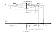
- FIG. 30B shows that in the illumination device of the present embodiment, the image of the surface light source is not blurred but formed in the irradiated area in a focused state on the same principle as the pan focus (that is, It is a figure for demonstrating the conditions where the shape of a surface light source, intensity
- l ′ (D / ( ⁇ + D)) ⁇ f ′.
- the effective diameter D is the effective diameter of the second lens L2.
- the distance l ′ from the second lens L2 to the virtual image I1 can be calculated from the distance from the light source 1 to the second lens L2 and the distance from the light source 1 to the virtual image l1.
- the distance from the light source 1 to the virtual image 11 can be calculated from the positional relationship between the light source 1 and the first lens L1, the refractive index of the first lens L1, the shape of the lens surface, and the like.
- the allowable confusion circle ⁇ in the pan focus can be regarded as a factor set according to the light emitting surface size of the surface light source when applied to the illumination device of the present embodiment.
- the allowable circle of confusion ⁇ can be regarded as a factor set by the arrangement pitch (intensity and chromaticity unevenness pitch).
- the permissible circle of confusion ⁇ in pan focus is defined by the size of the light emitting surface and the arrangement pitch of the light emitting elements, and these are referred to as “light source size factor ⁇ ”.
- the position of the reference focal point f ′ also changes depending on how the light source size factor ⁇ is set.
- FIG. 31 shows how the reference focus f 'changes according to the size of the light source size factor ⁇ .
- the reference focus f ′ as a condition that the intensity and chromaticity unevenness in the pitch order are visually recognized on the screen is compared. Set to the side closer to the target light source.
- the pattern (B) when a size larger than the pitch of the LED chips and smaller than the entire light source is considered as the light source size factor ⁇ , the reference focus f ′ is larger than that in the case of the pattern (A). Is set distally.
- the reference focal point f ′ is set further to the distal side than in the case of the pattern (B).
- the reference focal point f ′ is set farther from the light source
- the focal point F2 of the second lens L2 is set farther from the light source than the reference focal point.
- the factor ⁇ is smaller than the intensity and chromaticity unevenness of the LED light emitting surface (minimum pitch of arrangement of the LED elements)
- the image of the intensity and chromaticity unevenness is reflected on the screen. Since the light emission characteristics are different in the region surrounded by each of the two circles on the light emitting surface, the characteristics reaching the two circles on the screen are also different, and this is reflected as an image of the LED chip.
- the pattern (B) when a plurality of the above-described intensity and chromaticity irregularities are within the range of the factor ⁇ (more than the minimum pitch of the LED element arrangement), two circles on the light emitting surface The light emission characteristics of the area surrounded by are averaged, and the image of intensity and chromaticity unevenness is not visually recognized on the screen.
- the size of the LED light emitting surface exceeds the range of the factor ⁇ , the difference in intensity and chromaticity (that is, the shape of the LED light emitting surface) between the LED light emitting surface and the outer region is reflected, On the screen, an image having the shape of the LED light emitting surface may appear, which may be a problem.
- the factor ⁇ is a size including the entire light emitting surface, the shape of the light emitting surface is hardly reflected, and good irradiation is realized on the screen. .
- the light source size factor ⁇ may be set according to other forms. An example in which the light source size factor ⁇ is set in another form will be described below.
- FIG. 32 (a) shows a form in which red LEDs, blue LEDs, and green LEDs are arranged in a predetermined pattern.
- the LEDs of three different colors are set as one set, and the three-color LEDs are arrayed at the minimum pitch Pa repeatedly.
- the minimum pitch Pa as the light source size factor ⁇ , unevenness due to the arrangement of the three color LEDs in the irradiation region is prevented from being observed.
- FIG. 32B shows a case where the light emitting surface is formed in a pattern in which two types of vertically extending regions having different phosphor types, concentrations, thicknesses, and the like are repeated for each column.
- the characteristics of the respective light emitting elements may be the same, since the types of phosphors are different, the wavelength spectral characteristics emitted from the light emitting surface are different in the two types of regions.
- the repetition pitch minimum Pb of the arrangement every two rows may be set as the light source size factor ⁇ .
- the pitch can be the light source size factor ⁇ .
- the angular range of the irradiated light (the width of the irradiation region) depends on the positional relationship between the focal point F2 of the second lens and the virtual image I1 by the first lens L1. ) Will change.
- the optical lens can make the emission angle the narrowest when the light emission source exists at the focal position, and the emission angle becomes wider as the light emission source comes closer to the lens side than the focal position. In other words, the closer the position of the focal point F2 of the second lens and the virtual image I1 by the first lens L1, the narrower the irradiation angle, and the farther the virtual image l1, the wider the irradiation angle.
- This irradiation angle can be expressed by, for example, an orientation angle.
- the orientation angle is the width of a region having an illuminance of 50% or more with respect to the illuminance at the center of the irradiation region, where the illuminance at the center is 100% in the irradiation region formed on the screen. This is an angle calculated from (the diameter of a circular irradiation region when formed) and the distance between the light source and the screen.
- the orientation angle is small, it means that the illumination device emits light at a narrow angle, and when the orientation angle is large, it means that the illumination device emits light at a wide angle.
- the focal point F2 of the second lens is provided on the distal side of the reference position f ′, and in this case, for example, has an orientation angle of 8 degrees or more. An illumination device that irradiates irradiation light is obtained.
- the focal point F2 of the second lens L2 exists between the virtual image I1 formed by the first lens L1 and the virtual image I2 formed by the second lens L2.
- the focal point F2 is located closer to the light source than the focal point F1. Also in these forms, as long as the focal point F2 is provided farther from the reference position f ', an illuminance region having a uniform illuminance distribution can be formed.
- FIGS. 27D and 27E an illuminance region having a uniform illuminance distribution can be formed even when the focus F1 is located closer to the light source than the focus F2.
- FIG. 27E shows the focal points f1, f2 (F1, F2), the positions of the virtual images (I1, I2), and the synthetic focal point f1 + f2 (F (1 + 2)) in the embodiment shown in FIG. The positional relationship of each is shown.
- FIG. 27 (e) in the embodiment shown in FIG. 1, light can be irradiated at a wide angle so that the unevenness of intensity and chromaticity on the light emitting surface is not noticeable with a relatively large orientation angle.
- the focal point of the second lens As described above, by setting the focal point of the second lens to the distal side of the reference focal point f ′ obtained from the size factor ⁇ of the light emitting surface, the effective diameter D of the second lens, and the like, Reduced, that is, highly uniform illumination can be achieved.
- a mechanism for adjusting the effective aperture D of the second lens F2 may be provided.
- the focal length of the second lens is set so that the shape, intensity, and chromaticity unevenness of the light emitting surface are not reflected in the irradiation region with respect to any effective aperture D that can be taken.
- the optical system may be configured using a larger number of lenses.
- the first lens described above can be considered as a lens having the characteristics that the first to n ⁇ 1 lens groups have as a whole.
- the second lens may be considered as the nth lens.
- the shape of the optical lens included in the optical lens unit 2 in the illuminating device 11 may be determined by the arrangement of the focal position and the virtual image position in the vicinity of the optical axis. However, it is more preferable to determine the lens shape including the outside of the optical axis according to the following design policy.
- the light source 1 is optically adjacent to the light source 1 as much as possible. While approaching the lens, the paraxial theoretically corrects the off-axis coma with respect to the size of the surface light source while maintaining a virtual image relationship of approximately equal magnification system, and the spot diameter is the on-axis image point.
- the lens system is formed so that the off-axis image points have the same shape.
- Coma aberration refers to a phenomenon in which light emitted from one point away from the optical axis becomes an image like a comet with a tail rather than gathering at one point on the image surface.
- the condensed state is called a spot shape (spot diagram).
- the above-mentioned axis indicates the optical axis of the lens
- the on-axis indicates a place passing through the optical axis of the lens
- the off-axis indicates a place away from the optical axis.
- a paraxial theoretically approximately equal-magnification virtual image relationship means that the size of the L1 virtual image and L2 virtual image in FIG. 4A is one to several times that of the light source, and in the vicinity of the light source. The conditions for generating the L1 virtual image and the L2 virtual image are shown.
- correctioning off-axis coma means correcting by changing the off-axis lens shape so that light emitted from a place away from the optical axis gathers at one point on the image plane.
- the spot diameter is the same type for the on-axis image point and the off-axis image point” means that the range of the spot shape on the image plane of the light emitted from the axis and the light emitted from the axis is equivalent. As described above, correction is performed by changing the off-axis lens shape.
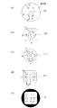
- the illuminance distribution on the evaluation surface is the result shown in FIG.
- the in-plane distribution is shown in monochrome according to the illuminance intensity
- the black display portion indicates the minimum illuminance
- the white display portion indicates the maximum illuminance.
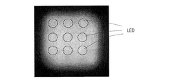
- the illuminating device of the present embodiment not only when the entire area of the light emitting surface of the light source 1 emits light uniformly, for example, as shown in FIG. Even when a plurality of light emitting surfaces are arranged, a predetermined illumination area can be illuminated uniformly. For example, it is conceivable to arrange a plurality of LED light emitters on the light emitting surface of the light source 1.
- light can irradiate the same irradiated area from any place on the light emitting surface, so even if there is a place where the amount of emitted light is small on a part of the light emitting surface, the uniformity of irradiation in the irradiated area is affected. This is because there is not.
- FIG. 9C shows the illuminance distribution by the light emitting surface of the light source 1 shown in FIG. From this illuminance distribution, it can be seen that the irradiation uniformity in the irradiation region is not affected.
- the plurality of minute light emitting surfaces in FIG. 9A may emit light having different main wavelengths, or may emit light having different main wavelengths.
- a plurality of luminescent materials may be combined. In that case, it is possible to realize an illumination device having a wide color reproducibility by irradiating the same illumination area almost uniformly with different color lights.
- the LED light source has a large variation in light emission characteristics such as a light emission amount, a light emission main wavelength, and a light emission wavelength region due to various variations in the manufacturing process of the light emitter.
- light emission characteristics such as a light emission amount, a light emission main wavelength, and a light emission wavelength region due to various variations in the manufacturing process of the light emitter.
- those having similar light emission characteristics are selected and used, but this selection work is a factor of cost increase.
- the uniformity of the irradiated region does not change even when one of the light emitting objects fails to be lit. Therefore, it is not necessary to replace the entire lighting device, and the usage time of the lighting device can be extended.
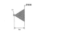
- the respective cross-sectional illuminance distributions at a distance of 1 m from the lighting device 11 and a distance of 5 m are as shown in FIGS. 11 (a) and 11 (b).
- FIG. 11A shows a cross-sectional illuminance distribution at a location 1 m away from the illumination device 11
- FIG. 11B shows a cross-sectional illuminance distribution at a location 5 m away from the illumination device 11.
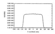
- the cross-sectional illuminance distribution of the light emitted from the illuminating device 11 has a uniform illuminance distribution at any position as long as it is more than a certain distance away.
- the certain distance or more is set to be twice or more the maximum diameter of the optical lenses L1 and L2 constituting the optical lens unit 2 of the illumination device 11.
- FIG. 12 a prototype example of the illumination device 11 shown in FIG. 1 is shown in FIG.
- a white LED package of about 6 mm ⁇ 6 mm was used as the light source 1.
- the second optical lens L2 is made of PMMA (polymethyl methacrylate) having a refractive index nd of about 1.49, the light incident surface is flat, the light exit surface has a radius of curvature of 20.966 mm, and the conic constant is 0. 28119, 4th order, 6th order, 8th order, 10th order, and 12th order higher aspheric coefficients are -5.2 ⁇ 10 ⁇ 7 , ⁇ 1.8914 ⁇ 10 ⁇ 8 , 3.4858 ⁇ 10 ⁇ 10, respectively. , ⁇ 9.7419 ⁇ 10 ⁇ 13 , 2.6235 ⁇ 10 ⁇ 16 , an optical lens manufactured with a lens outer shape of 35 mm and a lens thickness of 10.5 mm was used.
- PMMA polymethyl methacrylate
- the white LED package, the first optical lens L1, and the second optical lens L2 are arranged so that the centers of the white LED package and the second optical lens L2 coincide with each other on the optical axis.
- the distance from the light incident surface of the optical lens L1 of the eye is 1.5 mm, and the distance between the light exit surface of the first optical lens L1 and the incident surface of the second optical lens L2 is 2 on the optical axis. 0.0 mm.
- the focal lengths of the optical lenses L1 and L2 were 18.52 mm and 42.47 mm, respectively, and the combined focal length was 14.12 mm.
- the focal positions f1 and f2 and the combined focal positions f1 + f2 of the optical lenses L1 and L2 are ⁇ when the light emitting surface of the light source unit is 0 (origin) and the emission direction is an axis in the + direction. 11.30 mm, ⁇ 26.94 mm, and ⁇ 5.14 mm.
- the L1 virtual image was ⁇ 1.61 mm and the L2 virtual image was ⁇ 9.74 mm.
- the illuminating device 11 has the focal points f1 and f2 of the optical lenses L1 and L2 constituting each optical lens optical lens unit 2 for the virtual images (L1 virtual image and L2 virtual image) generated by the optical lenses L1 and L2.
- each virtual image (L1 virtual image, L2 virtual image) is present on the side opposite to the surface facing the light source 1, and it is confirmed that the design is as shown in FIG.
- FIG. 12B shows that the predetermined illumination area is illuminated with uniform illuminance.
- FIG. 2 a prototype example of the illumination device 11 shown in FIG. 2 is shown in FIG.
- a white LED package having a diameter of 2 mm was used as the light source 1.
- the sixth-order and eighth-order higher-order aspherical coefficients were ⁇ 5.97 ⁇ 10 ⁇ 5 , ⁇ 7.927 ⁇ 10 ⁇ 6 , and ⁇ 7.278 ⁇ 10 ⁇ 7 , respectively.
- the radius of curvature of the light exit surface is 8.0 mm
- the conic constant is 0.73
- the fourth-order, sixth-order, eighth-order, tenth-order, and twelfth-order higher-order aspheric coefficients are 1.225 ⁇ 10 ⁇ 4. -3.777 ⁇ 10 ⁇ 6 , ⁇ 1.054 ⁇ 10 ⁇ 7 , ⁇ 1.83 ⁇ 10 ⁇ 9 , 4.2397 ⁇ 10 ⁇ 11
- the lens outer shape is 10 mm
- the lens thickness is 3.0 mm. The produced optical lens was used.
- the white LED package, the first optical lens L1, and the second optical lens L2 are arranged so that the centers of the white LED package and the second optical lens L2 coincide with each other on the optical axis.
- the distance from the light incident surface of the optical lens L1 of the eye is 0.5 mm, and the distance between the light exit surface of the first optical lens L1 and the incident surface of the second optical lens L2 on the optical axis is 0. .1 mm.
- the focal lengths of the optical lenses L1 and L2 were 9,899 mm and 14.69 mm, respectively, and the combined focal length was 5.81 mm.
- the focal positions f1, f2 and the combined focal position f1 + f2 of the optical lenses L1, L2 are ⁇ when the light emitting surface of the light source unit is 0 (origin) and the emission direction is taken in the + direction. They were 6.76 mm, -10.68 mm, and -2.85 mm.
- the L1 virtual image was ⁇ 0.10 mm and the L2 virtual image was ⁇ 0.75 mm.
- the illumination device 11 having the above-described configuration causes the focal positions f1 and f2 of the optical lenses L1 and L2 and the combined focal position f1 + f2 to be virtual images (L1 virtual image and L2 virtual image) generated by the optical lenses L1 and L2, respectively.
- virtual images L1 virtual image, L2 virtual image
- all the virtual images exist on the side opposite to the surface facing the light source 1, and it was confirmed that the design was made as shown in FIG.
- FIG. 13B shows the result of an illuminance experiment performed using the illumination device 11 having the above configuration.
- a predetermined illumination area can be illuminated with uniform illuminance.
- FIG. 14 is a diagram illustrating a schematic configuration of the illumination device 12 according to the present embodiment.
- FIG. 15 is an enlarged view of the main part A shown in FIG.
- the illuminating device 12 has a structure in which optical lenses 3 and 4 are further added to the emission side of the optical lens unit 2 of the first embodiment.
- the illuminating device 12 has a second optical lens unit (optical lens 3, 4) is provided.
- the optical lens 3 is a concave lens, and is disposed closest to the optical lens unit 2 and with the concave side facing the optical lens unit 2.
- the optical lens 4 is a convex lens, and is disposed at a position farther from the optical lens unit 2 than the optical lens 3.
- the emission angle of the light emitted from the illumination device 12 can be narrowed.
- FIGS. 16 to 19 In the illumination device 12 having the above configuration, by optimizing the lens shape of the optical lenses 3 and 4 to be added, as shown in FIG. 16, it is possible to uniformly illuminate the irradiation area.
- the arrangement of the lens to be added is not limited to the arrangement position in FIG. 14 and may be another position.
- FIG. 17 is a diagram showing a schematic configuration of the illumination device 12 when the optical lenses 3 and 4 are arranged at positions different from the arrangement of the optical lenses 3 and 4 shown in FIG.
- FIG. 18 is an enlarged view of the main part B shown in FIG.
- the angular distribution of the light emitted from the illumination device 12 can be changed by arranging a part of the optical lenses 3 and 4 additionally arranged in FIG. 14 at different locations.
- the emission angle can be narrowed.
- the second optical lens unit is not limited to the optical lenses 3 and 4 shown in FIG. 14.
- the second optical lens unit is combined so as to have the same optical characteristics as the optical lens 3.
- a plurality of optical lenses may be used. There is no particular limitation on the number of optical lenses constituting the second optical lens unit.
- FIG. 20 is a diagram illustrating a schematic configuration of the illumination device 13a according to the present embodiment.
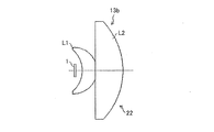
- FIG. 21 is a diagram showing a schematic configuration of the illumination device 13b according to the present embodiment.
- the optical lens unit 22 is formed by integrally molding the optical lenses L1 and L2.
- the optical lens portion 22 is formed by integrally molding the optical lenses L1 and L2 with a mold using a resin such as an acrylic material.
- the illumination device 13b shown in FIG. 21 shows an example in which the optical lenses L1 and L2 are bonded to form the optical lens unit 23.
- a lens (optical lens L1) close to the light emitting surface of the light source 1 and a lens far from the light emitting surface (optical lens L2) are respectively molded and then bonded near the center of each lens to form the optical lens unit 23. Yes.
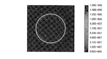
- FIG. 20 In the illuminating device 13a using the optical lens portion 22 when the optical lens is integrally molded, as shown in FIG. 22, it is parallel to the light emitting surface at a location 1 m away from the illuminating device 13a.
- the evaluation surface is arranged in FIG. 23, as shown in FIG.
- FIG. 24 shows a case where a hexagonal opening (aperture) portion 5 is provided on the light emitting side of the illumination device 11 of the first embodiment. Of the light emitted from the illuminating device 11, only the light directed to the hexagonal opening 5 is transmitted therethrough, and the other light is reflected and absorbed.
- FIG. 25 shows a two-dimensional illuminance distribution in the case where the evaluation surface is arranged at a distance of 1 m from the illuminating device 11, but is illuminated in substantially the same shape as the opening 5 and the illumination area has a uniform illuminance. It becomes possible to be illuminated with. Furthermore, even when the evaluation surface is separated from the surface light source illumination device, it is possible to illuminate while maintaining the shape and uniformity of the irradiation region.
- FIG. (1) The restriction
- the arrangement range of the light source 1 is more preferably limited to a range satisfying the following formula. h ⁇ 2 ⁇ (d (2R ⁇ d))
- h is the width of the light emitting portion arrangement range
- d is the distance from the light source to the optical lens L1 interface on the optical axis
- R is the inner lens radius of curvature of the optical lens L1.
- the light source 1 By disposing the light source 1 within the above range, it is possible to take all the light emitted from the light source 1 into the optical lens L1, which is the first lens, and to improve the light utilization efficiency.
- the focal position of the optical lens unit 2 arranged on the exit surface side of the light source 1 is behind the positions of the L1 virtual images and L2 virtual images generated by the optical lenses L1 and L2 (in the opposite direction to the lens exit side). ) In the distance, the position of the light source 1 and the virtual image (L1 virtual image, L2 virtual image) can be relatively moved closer to the optical lens unit 2.
- the lens principal point represents the position of the thin lens when the lens is replaced with a thin lens with negligible lens thickness, representing only the behavior of the light incident on and emitted from the lens.
- the virtual image position is brought closer to the optical lens unit 2 than the focal positions f1 and f2 of the optical lenses L1 and L2.
- the virtual image position is always relatively closer to the optical lens than the focal position of the optical lens. I can do it.
- anti-reflection surface treatment On the lens surface of each optical lens.
- a general anti-reflection surface treatment there is an anti-reflection film that reduces surface reflection by forming a plurality of thin films having different refractive indexes.
- a method of reducing interface reflection by forming a minute uneven shape (moth eye structure) of 1 micron or less on the lens surface of each optical lens.
- the method of reducing the interface reflection on the lens surface of each optical lens is not limited to the above method.
- the light emission wavelength of the light source unit is not limited to visible light.
- a light emitting element emitting a wavelength in the ultraviolet region or infrared region may be used.
- the lens shape is all a rotationally symmetric shape, but is not limited thereto, and may be a lenticular shape that is uniform in the depth direction of the drawing. This produces an effect only in a direction parallel to the lenticular lens cross-sectional direction. For example, it is suitable when a cold cathode tube or an LED lamp arranged in series is used as the light source.
- the uniform illumination area can be made into a rounded rectangle.
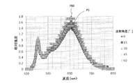
- FIG. 33 is a graph showing the relationship between the emission angle of light from the LED and the irradiation position when light from the surface light source 1 configured using the LED is irradiated through the lens.
- light emitted approximately in the front direction (emission angle 0 to 30 °) forms a mountain-shaped intensity distribution having a peak at the center of the irradiation region.
- the intensity distribution is formed so that the light emitted at a larger emission angle has a higher intensity in the peripheral area of the irradiation area.
- light emitted at an emission angle of 60 ° to 90 ° hardly reaches the central portion of the irradiation region, and most of the light is irradiated to the peripheral portion of the irradiation region.
- the spectrum of the light emitted from the LED changes depending on the emission angle. More specifically, the peak P60 of relative intensity at a wavelength of about 610 nm of light having a large emission angle (about 60 °) is a peak of relative intensity at a wavelength of about 610 nm of light in the front direction (output angle 0 °). Larger than P0. This is because light with a larger emission angle is obliquely incident on the phosphor provided so as to cover the LED, and therefore the distance that passes through the phosphor is longer than light that is incident straight, This is considered to be because the probability of causing fluorescence increases.
- the light emitted from the LED at a large emission angle includes a relatively large amount of long-wavelength components, and most of the light reaches the periphery of the irradiation region. As a result, a yellowish region is formed in the peripheral portion as compared with the central portion of the irradiation region.
- unintended light reflection and scattering may occur inside the illumination device, and stray light may be generated outside the irradiation area.
- Embodiments 4-1 to 4-6 described below a mode for preventing unwanted irradiation light observed in the periphery of the irradiation region as described above will be described.
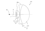
- FIG. 36 is a diagram illustrating a configuration of the illumination device 410 according to the embodiment 4-1.
- the illuminating device 410 is similar to the illuminating device described in the first to third embodiments, the surface light source 1, the first lens L1 disposed on the light emitting side of the surface light source 1, and the light emitting side of the first lens. And a second lens L2.
- the illumination device 410 is also configured to uniformly irradiate the irradiation area with the illumination device as described in the first to third embodiments. More specifically, the optical system is configured such that the virtual image I1 formed by the first lens L1 is positioned closer to the light source than the focal point F2 of the second lens L2. Also in the present embodiment, as described with reference to FIG. 29, the focal point F2 of the second lens L2 is provided on the distal side of the reference position f ′ determined in consideration of the size factor ⁇ . Yes. Thereby, the irradiation area
- the first lens L1 is composed of a concave lens L1-1 and a convex lens L1-2 arranged so as to be in close contact with each other without an air layer therebetween.
- the concave lens L1-1 and the convex lens L1-2 are formed of materials having different refractive indexes. By using these two lenses in combination, they can function as an achromatic lens for correcting chromatic aberration.
- the second lens L2 is also composed of a concave lens L2-1 and a convex lens L2-2 made of different materials, and can function as an achromatic lens.
- the concave lenses L1-1 and L2-1 are made of polycarbonate resin (PC) having a refractive index of 1.59, and the convex lens is used.
- L1-2 and L2-2 are made of polymethyl methacrylate resin (PMMA) having a refractive index of 1.49.
- the concave lenses L1-1 and L2-1 and the convex lenses L1-2 and L2-2 may be formed of other resin materials or inorganic materials such as glass.
- the refractive index difference of the concave-convex lens constituting the achromatic lens is 0.05 or more.
- a material having a relatively high refractive index it becomes easier to obtain an optical system in which the thickness of the lens is reduced and light from the light source 1 can be easily taken.
- the conventional achromatic lens is configured to correct chromatic aberration and form an image with high accuracy on the axis, but in this embodiment, it is not necessary to form an image at a specific position, and irradiation is performed on the periphery of the irradiation surface.
- the effect can be obtained by bringing the directions of the light beams of the respective wavelengths close to each other. For this reason, the tolerance of the lens shape change due to thermal expansion or the like is larger than in the case of image formation generally used in the past, and the resin-made lens having a larger linear expansion coefficient than the glass as described above. Combinations can be used.
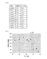
- Table 1 below gives specific design examples of the lenses L1-1, L1-2, L2-1, and L2-2.
- “coordinates” indicate the position of the light incident surface of each lens on the optical axis when the position of the light source 1 is the origin and the light emission side is the positive direction.
- the conic (outgoing side) in Table 1 indicates the value of the conic constant included in the aspheric function for defining the aspheric shape when an aspheric lens is used.
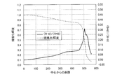
- FIGS. 37 (a) and (b) show the distance from the center of the illuminance region and the index of coloring for each of the illumination device 410 of this embodiment and the illumination device (reference example) that does not use an achromatic lens. It is a figure which shows the relationship with BR difference (RB) / (R + B).
- the BR difference is defined as 1 when the spectral radiance (normalized luminance) of the B light (wavelength 450 nm) and the R light (wavelength 610 nm) at the center of the irradiation region when the white screen is irradiated is 1, respectively.
- the spectral radiance (relative value) of R light and the spectral radiance (relative value) of B light at each point are measured, and (RB) / (R + B) is calculated from the measurement results.
- the yellow ring When subjectively evaluating the occurrence of yellow ring, when the BR difference is 0.3 or less, the yellow ring is not visually recognized under an illuminance of 100 lux, and the BR difference is 0.25 or less. The yellow ring was not visible under 50 lux illumination.
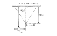
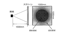
- the measurement of the spectral radiance described above is performed as shown in FIG. 35, in which the illumination device 410 is installed in the normal direction of the screen, and the spectral radiance meter SR3 is moved to the left and right to spectral radiance at each point on the screen.
- the spectral radiance of 450 nm and 610 nm measured at each point is normalized by the respective measured values at the center of the irradiation region, and thereby the BR difference (RB) / (R + B) can be obtained.
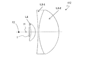
- FIG. 38 shows a modified illumination device 412.
- the illumination device 412 includes a light source 1, a first lens L1, and a second lens L2.
- the first lens L1 is composed of a single meniscus lens, and an achromatic lens composed of a combination of a concave lens L2-1 and a convex lens L2-2 is used only as the second lens L2. Yes.
- the optical system is designed so that the virtual image formed by the first lens L1 is positioned closer to the light source than the focal point F2 of the second lens L2.
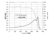
- the RB difference (RB) / (R + B) shows a relatively low value in the periphery of the irradiation region. In this way, the occurrence of yellow ring can be appropriately suppressed by simply using an achromatic lens as the second lens L2.
- Table 2 below gives specific design examples of the lenses L1, L2-1 and L2-2.
- the conic (outgoing side) in the table indicates the value of the conic constant when an aspherical lens is used.
- the modified illumination device 412 has a manufacturing advantage that the number of lens bonding steps is reduced. Moreover, since the number of lenses to be bonded is small, a large tolerance can be taken in design.
- a configuration may be adopted in which a light absorption layer or a reflection layer is provided on the end surface of the concave lens L2-1 to prevent stray light.
- the form using the achromat lens as the second lens L2 has been described.
- a form using the achromat lens as the first lens L1 and not using the achromat lens as the second lens is also conceivable.
- light passing through the second lens L2 may be affected by refractive index chromatic dispersion, and chromatic aberration may not be corrected appropriately.
- the second lens L2 can be reduced in thickness and weight.
- FIG. 39 shows the BR difference measured in the irradiation area formed by the illumination device 412.
- the BR difference (RB) / (R + B) is a relatively low value in the peripheral portion away from the center of the irradiation region. Indicates. Therefore, the occurrence of yellow ring is prevented appropriately.
- the lens is configured so that chromatic aberration can be reduced with respect to light transmitted through the peripheral portion of the lens, and chromatic aberration of light passing near the optical axis is not necessarily compensated. It is not necessary.
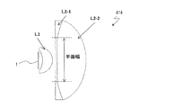
- FIG. 40 shows an illumination device 414 of this modification.
- the region where achromat is required (hereinafter sometimes referred to as an achromat portion) may be the outermost peripheral portion of the lens surface.
- 50% of the periphery of the lens radius may be an achromatic lens.
- the achromatic lens can be made lighter and thinner.
- the thickness of the concave lens L2-1 of the second lens L2 in the vicinity of the optical axis is set to 0.8 mm.
- the thickness at the center of the lens may be 0 mm, that is, a donut-shaped lens having a cavity at the center. This is because, in order to reduce the BR difference in the peripheral portion of the irradiation region, it is sufficient to achromatize the light passing through at least the lens outer peripheral region.
- a lens in which an achromat portion is formed only in a part thereof may also be referred to as an achromat lens.
- the peripheral portion of the lens may be an achromat lens, and even when the chromatic aberration of only the peripheral portion is corrected, the occurrence of yellow ring can be prevented.
- a normal achromatic lens is designed to correct chromatic aberration on the optical axis, but this configuration is different from conventional achromatic lenses in that it is designed to correct chromatic aberration of non-axial rays. .
- FIG. 41 shows the BR difference measured in the irradiation area formed by the illumination device 414.
- the BR difference (RB) / (R + B) is compared in the periphery away from the center of the irradiation area. Low value. Therefore, the occurrence of yellow ring is prevented appropriately.
- ⁇ Embodiment 4-2 Form in which a light diffusion layer is provided between a light source and a lens> Fig.42 (a) has shown the vicinity of the light source 1 with which the illuminating device of this embodiment is provided, and the diffusion layer 40a which has translucency on the sealing layer 1b which seals several LED chip 1a is shown. Is provided.
- the diffusion layer 40a has a large number of fine irregularities that are typically irregularly arranged on the surface thereof.
- FIG. 42 (b) shows the vicinity of the light source 1 provided in the illumination device of the modification, and is formed from a transparent resin containing a plurality of fine particles on the sealing layer 1b for sealing the LED chip 1a.
- a diffusion layer 40b is provided.
- an optical element that scatters and diffuses light is disposed between the light source 1 and the first lens L1.
- Table 4 shows the occurrence of peripheral chromaticity unevenness and coloring in Examples (a) and (b) corresponding to FIGS. 42 (a) and (b) and other Examples (c1) to (c5). Results and light utilization efficiency are shown.
- a diffusion layer is provided between the light source and the first lens in the same manner as in Examples (a) and (b), and the haze value of the diffusion layer is set in the range of 3% to 70%. is doing.
- Table 4 also shows a case where a diffusion layer is provided between the first lens L1 and the second lens L2 as a comparative example.
- the haze value is preferably set to 5% to 50%.
- the haze value is set to 5% to 30%, the effect of eliminating color unevenness in the irradiated area can be obtained simultaneously with the elimination of peripheral coloring.
- the “haze value” is a value indicating “cloudiness”.
- the haze value is defined by the following equation when the total light transmittance is Tt (%) and the diffuse transmittance is Td (%).
- Haze value (%) (Td / Tt) ⁇ 100
- the total light transmittance Tt is a ratio of the total intensity of the diffuse transmitted light and the parallel transmitted light to the incident light (parallel light) intensity.
- the diffuse transmittance Td is a ratio of the intensity of diffuse transmitted light to the intensity of incident light (parallel light).
- the lightness of the light diffusion layer increases as the haze value decreases, and the haze value of the light diffusion layer increases as the haze value increases.
- the haze value can be measured by, for example, an integrating sphere light transmittance measuring device.
- FIG. 43A shows a general light source (comparative example) used in the LED illumination device
- FIGS. 43B to 43E show various light sources used in the illumination device of the present embodiment.
- each light source a plurality of LEDs are arranged so as to be separated from each other at an interval of a pitch P.
- the light source is provided with a phosphor together with the LED.
- the phosphor is provided in a layered manner so as to cover, for example, a plurality of LEDs so as to appropriately generate fluorescence upon receiving light from the LEDs.
- the yellow ring can be reduced by making the phosphor formation region outside the LED smaller (here, B ⁇ P).
- the phosphor formation region is different between the corner portion and the other portions. As a result, shades of yellow rings may occur around the irradiated area.
- the distance to the edge of the phosphor formation region outside the LED is set to be approximately equal at any place, and this is the pitch.
- the distance to the edge of the phosphor formation region outside the LED is set to be approximately equal at any place, and this is the pitch.
- the distance less than or equal to P that is, by setting A ⁇ P and B ⁇ P
- the yellow ring can be more effectively reduced.
- a light shielding layer may be formed, and the light emitting surface of the phosphor may be the same as that shown in FIG. 43 (d).
- the yellow component of the spectrum of light emitted from the peripheral portion of the light source can be reduced, and the yellow ring and chromaticity unevenness can be reduced. Occurrence can be suppressed.
- FIG. 44 shows the BR difference measured in the irradiation area formed when the light source shown in FIG. 43 (c) is used.
- the BR difference (RB) / (R + B) shows a relatively low value in the peripheral portion away from the center of the irradiation region, and accordingly, the occurrence of yellow ring is appropriately prevented. Is done.
- ⁇ Embodiment 4-4 Form in which a lens hood is provided>
- a cylindrical hood 48 is provided as a light shielding member on the light emitting side of the illumination device 440.
- Lf2 of the hood 48 by appropriately adjusting the length Lf2 of the hood 48 according to the orientation angle of the light emitted from the lighting device 440, stray light generated around the irradiation region can be prevented while keeping the light use efficiency high. can do.
- FIG. 45 shows the relative illuminance at the periphery of the irradiated area.
- the illuminance rapidly decreases at the edge portion of the irradiation region.
- a stray light region formed by stray light is formed around the irradiation region.
- Stray light is considered to be generated by unintentional reflection of light in the optical system or light transmitted through the end face of the lens. Such stray light is observed around the intended irradiation area, and it is desired to prevent the stray light from occurring in the lighting device.
- the irradiation area has a relative illuminance of 0.10 in the angle-relative illuminance graph shown in FIG. 45 when light is irradiated onto a screen (size 1 m ⁇ 1 m) 1 m away from the illumination device.
- An area inside the intersection of the tangent line and the X axis (angle) is meant.
- the stray light region means a region outside the irradiation region defined as described above.
- the stray light ratio means the ratio of stray light in the entire irradiation light expressed by the luminous flux in the stray light area / (the luminous flux in the irradiation area + the luminous flux in the stray light area).
- the illumination device 440 includes the light source 1, the first lens L1, and the second lens L2 that is an achromatic lens, as described in the embodiment 4-1.
- the second lens L2 includes a concave lens L2-1 and a convex lens L2-2 combined therewith.
- the light source 1, the first lens L 1, and the second lens L 2 are held in the housing space of the housing 47.
- Table 5 shows design examples of the first lens and the second lens. However, it goes without saying that various other designs are possible.
- the aspheric coefficient quartic and the aspheric coefficient sixth are the aspheric coefficients of the fourth and sixth terms for defining the aspheric surface when an aspheric lens is used, respectively. Yes.
- the illumination device 440 further includes a hood 48 provided so as to surround the light emitting surface of the second lens L2, and the hood 48 is fixed to the housing 47.
- the hood 48 is made of, for example, a resin or a metal material, and typically has an inner surface side configured to absorb light.
- substantially uniform illuminance is realized inside the predetermined irradiation area, and the illuminance rapidly decreases outside the irradiation area.
- stray light can be effectively reduced while suppressing loss of light irradiated to the irradiation region.
- hood 48 If the hood 48 is too long, not only stray light but also a part of the irradiation light is absorbed or scattered, so that the light utilization efficiency is greatly reduced. On the other hand, if the hood is too short, stray light that reaches the periphery of the irradiation region cannot be prevented.
- Example 4 (a) and (b) when there is no hood, the utilization efficiency is high, but the stray light ratio is large and the stray light cannot be sufficiently suppressed. Therefore, when a hood having a length of 40 mm or 60 mm is provided as shown in Example 4 (a) and (b), stray light can be prevented without significantly reducing the utilization efficiency, and the stray light ratio is 3 % Or less can be realized. However, if the hood length is as long as 80 mm, the light utilization efficiency is significantly reduced, which may not be preferable.
- the length of the hood may be determined according to the emission angle ⁇ 1, the emission angle ⁇ 2, and the hood radius Rf shown in FIG.
- the upper limit L2y of the length of the hood can be defined by using the emission angle ⁇ 1 at which the relative illuminance on the screen rapidly decreases.
- ⁇ 1 may be set to the minimum angle at which the slope of the angle-relative illuminance graph shown in FIG. 48 is smaller than ⁇ 0.1.
- ⁇ 1 is 25 °.
- the hood length upper limit L2y Rf / tan ⁇ 1-Lf1
- Lf1 is a distance on the optical axis from the surface light source 1 to the end of the housing (connection portion with the hood 48). That is, the distance from the surface light source 1 to the tip of the hood on the optical axis can be represented by Lf1 + Lf2.
- the hood When the hood is longer than the upper limit L2y, the light that should reach the irradiation area is blocked by the hood. Accordingly, there is a possibility that the light use efficiency is greatly reduced, and that the steep fall of the illuminance at the irradiation region edge cannot be realized.
- ⁇ 2 38 ° is determined by measuring illuminance as an angle at which the stray light ratio becomes 1%.
- the hood length lower limit L2s is obtained by the following equation.
- L2s Rf / tan ⁇ 2-Lf1
- the hood When the hood is shorter than the lower limit L2s, there is almost no light blocked by the hood out of the light reaching the periphery of the irradiation area. For this reason, the hood having a length equal to or shorter than the lower limit L2y can hardly block stray light generated around the irradiation region.
- the length L2f of the hood alone (or the distance L1f + L2f on the optical axis from the surface light source to the hood end) is preferably set so as to satisfy the following expression.
- the light distribution characteristic is not a Gaussian distribution, and the stray light region and the irradiation region are distinguished, so that only the stray light can be efficiently reduced by appropriately configuring the shape of the hood. Can be able to.
- ⁇ Embodiment 4-5 Form in which a reflective layer is provided on the lens surface>
- the antireflection layer 50 (on the light incident side surface and / or the light output side surface of the first lens L1 provided on the illumination device 450 and on both side surfaces of the second lens L2).
- the AR layer 50 may be provided.
- Table 7 below shows the stray light ratio, light utilization efficiency, etc. when the AR layer 50 is provided on at least one of the exit side surface of the first lens L1, the entrance side surface of the first lens L1, and both side surfaces of the second lens L2. Indicates.
- the cup reflectance in Table 7 indicates the reflectance of the inner surface of the housing 47 that accommodates the first lens L1 and the second lens L2, and in this embodiment, no antireflection treatment is particularly performed. In all the examples, it is set to 90%.
- Comparative Example 5 a form in which neither the first lens L1 nor the second lens L2 is provided with an AR layer is shown. It is shown that when the AR layer is not provided, the reflectance of the lens surface is 4%.
- the AR layer 50 is provided so that the reflectance of the exit side surface of the first lens L1 is 2%, 1%, and 0.5%, respectively.
- the reflectance described in the table is the front reflectance in the D65 light source.
- AR is set so that the reflectances of both the exit side surface and the entrance side surface of the first lens L1 are 2%, 1%, and 0.5%, respectively.
- a layer 50 is provided.
- the reflectivity of both the exit side surface and the entrance side surface of the first lens L1 and the exit side surface and the entrance side surface of the second lens L2 is 2%. % And 0.5% of AR layer 50 is provided.
- design examples of each lens in the present embodiment are as shown in Table 8 below.
- the first lens L1 is the lens closest to the light source.
- the form using the meniscus lens as the 1st lens L1 is shown in FIG. 49, it is not restricted to this.
- an achromatic lens composed of two concave and convex lenses is used as the first lens L1
- an integrated lens can be considered as the first lens L1.
- the lens closest to the light source may be considered as the first lens L1
- one of the other lenses may be considered as the second lens L2.
- the illumination device 450 of the present embodiment there are at least four interfaces between the lens, air, and the interface.
- installing an antireflection layer causes an increase in manufacturing process and cost.
- the antireflection layer As a result of analyzing the generation source of stray light in order to identify the surface on which the antireflection layer is most preferably provided, about 80% or more of stray light is generated by reflection at the lens-air interface on the exit side surface of the first lens L1. I found out. For this reason, it is preferable to provide an antireflection layer at least on the irradiation surface side of the first lens L1.
- the stray light ratio can be further reduced by providing an AR layer on another lens surface. Note that these structures are advantageous structures, especially when the AR layer is formed by the DIP method, because the manufacturing cost is not significantly increased.
- ⁇ Embodiment 4-6 Form in which a light absorption layer is provided inside the edge or housing>
- an absorption layer Lsa is provided on the edge of the first lens L1 and the second lens L2.
- the edge means a side surface portion of a lens edge (typically a surface forming a cylindrical side surface).
- the absorbing layer Lsa is formed by painting the edge of the lens black.
- Example 6 (a) is a structure which provided the absorption layer further in the edge in the structure of Example 5 (b).
- Examples 6 (b) and (c) are the configurations of Example 5 (e) and Example 5 (h), in which an absorption layer Lsa is further provided on the edge.
- Example 6 (d), (e), (f) is a structure which provided the absorption layer further in the edge in the structure of Example 5 (c), (f), (i).
- Example 6 (g), (h), (i) is the structure of Example 6 (b), (e), (h), and is the structure which further provided the absorption layer in the cup (inside the housing). is there. By providing an absorption layer on the cup, the reflectivity is reduced to 5%.
- stray light can be further reduced by providing an absorption layer on the edge, and the stray light ratio can be reduced to 1.6% or less.
- stray light can also be reduced by scattering the surface of the edge instead of providing an absorption layer on the edge.
- the reflectance of the absorbing layer provided on the edge is preferably set to 10% or less.
- stray light can be reduced by reducing the reflectance inside the housing.
- Embodiment 4-4 Like the illumination device 462 shown in FIG. 51, the hood shown in the embodiment 4-4 is provided, and further, the reflection layer is provided on the lens surface as shown in the embodiments 4-5 and 4-6, and / or Alternatively, an absorption layer may be provided on the edge.
- Example 7 (h) shows Examples 7 (a) to (h) and Comparative Example 7.
- stray light can be reduced by painting the inside of the housing black as in the lighting device 464 shown in FIG. 52, and the stray light ratio can be reduced to 1.5% or less.
- Table 11 below shows Examples 8 (a) to (l) and Comparative Example 8. By coating the inside of the casing with black, the cup reflectance is reduced from 90% to 5%.
- the lighting device of the present embodiment has the same configuration as the lighting device shown in FIG. That is, as shown in FIG. 1, the illumination device includes a light source (light emitting unit) 1 and an optical lens unit 2 a disposed on the optical axis Ax on the light emitting surface side, which is the light extraction side of the light source 1. The light emitted from the light source 1 is irradiated through the optical lens unit 2 (first optical lens unit) a.
- the light source 1 includes an LED light emitter that is a surface light emitter that performs surface light emission.
- an LED light emitter that is a surface light emitter that performs surface light emission.
- it if it is a surface light-emitting body which performs surface light emission, it will not be limited to a LED light-emitting body.
- a remote phosphor structure in which a light emitting unit including a phosphor is used as the light emitting unit and the light source and the light emitting unit are separated may be employed.
- the shape of the light emission surface of the LED light emitter (surface light emitter) of the present embodiment is a rectangular shape, and the area of this rectangle is about 6 mm ⁇ 6 mm.
- the optical lens L1 has a diameter that is at least larger than the maximum width of the light emitting surface of the light source 1, and is composed of an optical lens having a concave surface on the light source 1 side.
- the thickness with respect to the optical axis Ax direction 5.0 mm
- the diameter of the cross section (maximum) perpendicular to the optical axis Ax 12.0 mm
- the radius of curvature of the entrance surface (concave) 9.2 mm
- the exit surface ( Convex) radius of curvature 6.0 mm.
- crown glass for example, BK7 manufactured by Schott: Abbe number 64.7, etc.
- an olefin resin for example, ZEONEX, JSR manufactured by ZEON Corporation.
- the optical lens L2 has a diameter larger than the maximum diameter of the optical lens L1, which is at least the first optical lens, and is a lens having a convex shape on the light exit surface side.
- the thickness with respect to the optical axis Ax direction 10.5 mm
- the diameter of the cross section (maximum) perpendicular to the optical axis Ax 35.0 mm
- the incident surface plane
- the exit surface (convex) radius of curvature 21 mm
- aspheric coefficient fourth order ⁇ 5.2 ⁇ 10 ⁇ 7
- aspheric coefficient sixth order ⁇ 1.9 ⁇ 10 ⁇ 8
- aspheric coefficient eighth order 3.5 ⁇ 10 ⁇ 10
- aspheric coefficient 10th order ⁇ 9.7 ⁇ 10 ⁇ 13
- aspheric coefficient 12th order 2.6 ⁇ 10 ⁇ 16 .
- PMMA is used as a constituent material of the optical lens L2, but it is not limited to this.
- examples of the candidate other than PMMA include the above-mentioned crown glass and olefin resin.
- the white LED package, the first optical lens L1, and the second optical lens L2 are arranged so that the centers of the white LED package and the second optical lens L2 coincide with each other on the optical axis.
- the distance from the light incident surface of the optical lens L1 of the eye is 1.5 mm, and the distance between the light exit surface of the first optical lens L1 and the incident surface of the second optical lens L2 is 2 on the optical axis. 0.0 mm.
- the focal lengths of the optical lenses L1 and L2 were 23.05 mm and 42.47 mm, respectively, and the combined focal length was 16.14 mm.
- the focal positions f1 and f2 and the combined focal positions f1 + f2 of the optical lenses L1 and L2 are ⁇ when the light emitting surface of the light source unit is 0 (origin) and the emission direction is an axis in the + direction. They were 15.20 mm, ⁇ 26.94 mm, and ⁇ 6.44 mm.
- the L1 virtual image was ⁇ 1.26 mm and the L2 virtual image was ⁇ 8.76 mm.
- PMMA is used as a lens constituent material.
- the refractive indexes for light with wavelengths of 587.6 nm, 486.1 nm, and 656.3 nm are respectively set.
- each of the optical lenses L1 and L2 may be a material having translucency and does not necessarily need to be colorless and transparent.
- the constituent materials of the optical lenses L1 and L2 are preferably materials having heat resistance. Thereby, it can suppress that a lens deform
- the present inventor newly found out that a phenomenon (coloring phenomenon) in which the end of the irradiation area becomes a different color from the vicinity of the center occurs when the irradiation surface is made close to uniform with the light source of Patent Document 1 described above. Therefore, the present inventors diligently studied the cause of the above-mentioned coloring phenomenon, and it was newly found that the degree of coloring increases as the Abbe number of the constituent material of the lens decreases. Qualitatively, it is considered that the lower the Abbe number, the larger the difference in refractive index due to the difference in the wavelengths of a plurality of lights having different wavelengths passing through the lens.
- the Abbe number of each constituent material of the optical lenses L1 and L2 is 54 or more (a relatively high Abbe number; in this embodiment, PMMA is used and the Abbe number is 58).
- the difference in refractive index due to the difference in wavelength of the plurality of light beams having different wavelengths passing through the optical lenses L1 and L2 constituting the optical lens portion 2a is reduced, so that the light beams of the plurality of light beams having different wavelengths can be reduced. Deviation is reduced. For this reason, the color change near the center of the irradiation area and at the end can be reduced.
- the lighting device of the present embodiment may have the same configuration as the lighting device shown in FIG.
- the advantage of using a lens whose Abbe number is appropriately selected as described above will be described.
- the Abbe number of each constituent material of the optical lenses L1 and L2 is 54 or more (relatively high Abbe number; in this embodiment, PMMA is used. Abbe number 58).
- the difference in refractive index due to the difference in the wavelengths of the plurality of light beams having different wavelengths passing through the optical lenses L1 and L2 constituting the optical lens portion 2a is reduced, so that the light beams between the light beams having different wavelengths can be reduced. Deviation is reduced. For this reason, the color change near the center of the irradiation area and at the end can be reduced.
- FIG. 53 (a) is a diagram showing the light beam behavior of the illumination device 11a of the present embodiment.
- FIG. 53B is a diagram showing the light beam behavior of the illumination device (collimating optical system LC2) of the reference example (sample 2).
- FIG. 53C is a table showing the relationship between the constituent materials of each lens and the refractive index or Abbe number.
- the tracking results of the light beams of red light (wavelength 700 nm; thin solid line) and blue light (wavelength 435 nm; dark solid line) emitted from the light source 1 in the lighting apparatus 11a and the lighting apparatus of the reference example are shown.
- FIG. 54A shows the illuminance distribution when the illumination device 11a includes three types of light of the light bulb color (3000K), blue (wavelength 435 nm), and red (wavelength 700 nm) in the irradiation light.
- FIG. 54B shows the illuminance distribution of the collimating optical system LC2 of the reference example.
- FIG. 54C shows a color chart of the lighting device shown in FIG.
- the illumination device 11a has a uniform illuminance area, and there is almost no difference between the illuminance areas of red light and blue light even 1000 mm away. ) The color change near the center and at the edge is almost unknown.
- a low Abbe number material (polycarbonate (PC); Abbe number 30) is used for the optical lens L1 as in the illumination device of the collimating optical system LC2.
- the areas (color change distances) where the difference occurs between the light beams of red light and blue light are different.
- the color change distance is about 70 mm in the illumination device 11a, whereas the color change distance is about 120 mm in the collimating optical system LC2, that is, the colored area around the irradiation area becomes large.
- FIG. 55 (a) is a table showing the relationship between the constituent materials of the lens, the refractive index, and the Abbe number.
- FIG. 55B is a graph showing the relationship between the Abbe number and the color change distance at the end (periphery) of the irradiation area.
- the inventor made the Abbe number and the color change distance at the end (periphery) of the irradiation area for each material shown in the table of FIG. The relationship was evaluated.
- the color change distance is approximately 112 mm or more, or approximately 120 mm or more.
- the distance of color change is 96 mm or less, or almost 68 mm or less.
- the Abbe number is preferably 54 or more and 82 or less, and more preferably 56 or more and 65 or less.
- ⁇ Embodiment 5-2> 56 and 57 are diagrams showing a schematic configuration of the illumination device 11c according to the present embodiment.
- an optical lens unit 2b including two optical lens L3 and L4 that are irradiation angle adjusting lenses is provided on the light emission side of the optical lens unit 2a. It differs from said illuminating device 11a, 11b by the point.
- optical lens unit 2a Since the optical lens unit 2a is as described above, the optical lens unit 2b will be described below.
- the optical lens portion 2b is composed of two optical lenses L3 and L4, and has a structure in which the optical lens L3 and the optical lens L4 are arranged in order from the side closer to the light emitting side of the optical lens portion 2a.
- the optical lenses L3 and L4 are arranged so that their centers pass through the optical axis Ax.
- the optical lens L3 has a diameter that is at least larger than the diameter of the cross section (maximum) perpendicular to the optical axis Ax of the optical lens L2, and is composed of an optical lens having a concave surface on the optical lens L2 side.
- thickness with respect to the optical axis Ax direction 10 mm
- diameter of the cross section (maximum) perpendicular to the optical axis Ax 50 mm
- curvature radius of the incident surface (concave) 78 mm
- curvature radius of the exit surface (convex) 180 mm.
- the constituent material of the optical lens L3 is preferably a high Abbe number like the optical lenses L1 and L2, and PMMA is used in this embodiment, but is not limited thereto.
- examples of the candidate other than PMMA include the above-mentioned crown glass and olefin resin.
- the distance between the optical lenses L2 and L3 is variable within a range not interfering with the optical lenses L2 and L4. As shown in FIGS. 57A and 57B, irradiation is performed by changing this distance. The angle can be adjusted to change to a wide angle or a narrow angle.
- FIG. 57 (a) shows the arrangement of each lens when the illumination angle of the illumination light is a narrow angle.
- FIG. 57B shows the arrangement of the lenses when the illumination angle of the illumination light is a wide angle.
- the optical lens L4 has a diameter larger than the maximum diameter of the optical lens L3, which is at least the first optical lens, and is a lens having a convex shape on the light exit surface side.
- thickness with respect to the optical axis Ax direction 18 mm
- diameter of the cross section (maximum) perpendicular to the optical axis Ax 100 mm
- curvature radius of the incident surface (concave) 330 mm
- curvature radius of the exit surface (convex) 90 mm.
- PMMA is used as a constituent material of the optical lens L4, but is not limited thereto.
- examples of the candidate other than PMMA include the above-mentioned crown glass and olefin resin.
- the distance between the optical lenses L2 to L4 shown in FIG. 56 is about 50 mm.
- FIG. 58 (a) shows an illuminance distribution when a narrow-angle lens arrangement includes three types of light of light bulb color (3000K), blue (wavelength 435nm), and red (wavelength 700nm) in the irradiated light.
- FIG. 58B shows a color chart.
- FIG. 59 (a) shows the illuminance distribution when three types of light of light bulb color, blue and red are included in the irradiation light in the wide-angle lens arrangement. Further, FIG. 59B shows a color chart.
- the illumination device 11c has a uniform illuminance area, and there is almost no difference between the illuminance areas of red light and blue light even 1000 mm away. The color change of the part is hardly understood.
- FIG. 60 is a diagram showing a schematic configuration of the illumination device 11d according to the present embodiment.
- the illuminating device 11d includes a light source 1 (light emitting unit) and an optical lens unit 2c in which two optical lenses L1 and L2 are integrated.
- the light source 1 includes an LED light emitter that is a surface light emitter that performs surface light emission.
- an LED light emitter that is a surface light emitter that performs surface light emission.
- it if it is a surface light-emitting body which performs surface light emission, it will not be limited to a LED light-emitting body.
- a light emitting unit including a phosphor may be used as the light emitting unit, and a structure in which the light source and the light emitting unit are separated may be employed.
- the shape of the light emission surface of the LED light emitter (surface light emitter) of the present embodiment is a substantially circular shape, and the diameter is 2 mm ⁇ .
- optical lens part 2c The light emitted in the direction perpendicular to the light emitting surface of the light source 1 is substantially perpendicularly incident on each air interface of the optical lens L2. Therefore, as shown in the figure, even if a part near the center of each of the optical lenses L1 and L2 is contacted or joined, the uniformity of the irradiation area is realized without greatly affecting the emission angle distribution. Is done.
- the optical lens L1 has a diameter that is at least larger than the maximum width of the light emitting surface of the light source 1, and is composed of an optical lens having a concave surface on the light source 1 side.
- the thickness with respect to the optical axis Ax direction 2.0 mm
- the diameter of the cross section (maximum) perpendicular to the optical axis Ax 8.0 mm
- the radius of curvature of the incident surface (concave) 6.6 mm
- the exit surface ( Convex) radius of curvature 4.0 mm.
- the constituent material of the optical lens L1 is PMMA as described above, but is not limited thereto.
- examples of the candidate other than PMMA include the above-mentioned crown glass and olefin resin.
- the optical lens L2 has a diameter larger than the maximum diameter of the optical lens L1, which is at least the first optical lens, and is a lens having a convex shape on the light exit surface side.
- the thickness with respect to the optical axis Ax direction 4.0 mm
- the diameter of the cross section (maximum) perpendicular to the optical axis Ax 16 mm
- the incident surface flat
- the exit surface (convex) curvature radius 12 mm
- the output surface The (convex) conic constant is -0.20.
- PMMA is used as a constituent material of the optical lens L2, but it is not limited to this.
- examples of the candidate other than PMMA include the above-mentioned crown glass and olefin resin.
- the optical lenses L1 and L2 are integrally molded or the optical lenses L1 and L2 are joined to form the optical lens portion 2c.
- Integrated molding Specifically, the optical lenses L1 and L2 are integrally molded with a resin such as an acrylic material (in this embodiment, PMMA having an Abbe number of 58 is used) to form an optical lens portion 2c.
- Bonding On the other hand, after molding a lens (optical lens L1) close to the light emitting surface of the light source 1 and a lens (optical lens L2) far from the light emitting surface, the optical lens unit is bonded near the center of each lens. It may be 2c.
- the manufacturing method of the illuminating device 11d includes the following steps.
- each of the plurality of optical lenses created in the lens creation step (a) is joined by adjusting the optical axis.
- the optical lens having two lenses is integrated by bonding using an adhesive, but the present invention is not limited to this.
- welding welding, pressure bonding, and the like can be listed.
- FIG. 61A shows the illuminance distribution when the irradiation light includes three types of light of a bulb color (3000 K), blue (wavelength 435 nm), and red (wavelength 700 nm).
- FIG. 61B shows a color chart.
- the illuminance area is uniform, and there is almost no difference between the illuminance areas of red light and blue light even 1000 mm away, so the color change near the center and the edge is hardly noticed.
- the optical lens unit including a plurality of optical lenses is arranged on the light extraction side of the light emitting unit
- the optical lens unit is provided for each optical lens. Is located on the opposite side of the surface facing the light emitting portion with respect to each virtual image generated by each optical lens, and the Abbe number of each constituent material of the plurality of optical lenses is It may be 54 or more.
- the manufacturing method of the lighting device is a manufacturing method of a lighting device in which an optical lens unit including a plurality of optical lenses is arranged on the light extraction side of the light emitting unit, and the light transmission has an Abbe number of 54 or more.
- a virtual image by each lens can be generated at a position close to the light emitting unit.
- the light emitted from the center of the light emitting unit existing on the optical axis of the optical lens unit and the light emitted from the position deviated from the center of the light emitting unit are emitted from the optical lens unit with substantially equal angular distribution. Therefore, the light emitted from the center of the light emitting unit and the light emitted from a position deviating from the center of the light emitting unit can be irradiated in the same manner over the entire irradiation region, so that the irradiation region is uniform. It is possible to dramatically improve the performance.
- the light emitted from the center of the light emitting unit and the light emitted from a position deviating from the center of the light emitting unit can be emitted from the optical lens unit with a substantially equal angular distribution, and thus are not emitted to the optical lens unit. Light can be almost eliminated, and as a result, high light utilization efficiency can be realized.
- the Abbe number of each constituent material of the plurality of optical lenses is 54 or more (a relatively high Abbe number).
- the difference in refractive index due to the difference in wavelength of the plurality of light beams having different wavelengths passing through each of the plurality of optical lenses constituting the optical lens unit is reduced, so that there is a shift between the light beams of the plurality of light beams having different wavelengths. Get smaller. For this reason, the color change near the center of the irradiation area and at the end can be reduced.
- the uniformity of the irradiated area can be dramatically improved, and the color change between the center of the spot of the irradiated light and the edge can be reduced.
- the illumination device is a combination of the focal points of the optical lenses constituting the optical lens unit in the illumination device in which a lens unit including a plurality of optical lenses is arranged on the light irradiation surface side of the light emitting unit.
- the focal position may be present on the opposite side of the surface facing the light emitting portion of all the virtual images with respect to the virtual images generated by the optical lenses.
- the combined focal position obtained by combining the focal points of the optical lenses constituting the optical lens unit is set in the light emitting units of all the virtual images with respect to the virtual images generated by the optical lenses.
- a virtual image by each lens can be generated at a position closer to the light emitting unit.
- the angle of light emitted from the optical lens unit can be expanded, so that the uniformity of a wider irradiation area can be dramatically improved.
- a virtual image by each lens can be generated at a position close to the light emitting unit, so almost all of the light emitted from the light emitting unit can be used, and high light utilization efficiency is achieved.
- the difference in refractive index due to the difference in the wavelengths of the plurality of light beams that pass through each of the plurality of optical lenses constituting the optical lens unit is reduced, so that the light beams of the light beams having different wavelengths can be obtained.
- the gap between them is reduced. For this reason, the color change near the center of the irradiation area and at the end can be reduced.
- the constituent material of each of the plurality of optical lenses may be a material having heat resistance.
- a second optical lens unit may be provided on the light emission side of the first optical lens unit.
- the emission angle of the light emitted from the first optical lens unit can be changed by the second optical lens unit. That is, by adjusting the optical characteristics of the second optical lens unit, it is possible to narrow or widen the emission angle of the light emitted from the first optical lens unit.
- the second optical lens unit may be configured with a concave lens as a lens closest to the first optical lens unit and a convex lens as a lens next to the second optical lens unit.
- the aberration generated in each lens can be corrected by the combination of the concave lens and the convex lens, the characteristics of the light emitted from the first optical lens unit can be prevented from being destroyed.
- the emission angle of the light emitted from the first optical lens unit can be adjusted, and almost all the light emitted from the light emitting unit can be used, realizing high light utilization efficiency. It is possible to irradiate substantially the same irradiation area with light emitted from different places of the light emitting section, and the uniformity of the irradiation area can be dramatically improved.
- each lens interface may be integrally formed in the optical lens unit.
- each lens constituting the optical lens unit since a part of each lens constituting the optical lens unit is integrally formed, the light emitting surface of the light emitting unit and the optical lens unit can be easily aligned.
- the light emitting part and the optical lens part can be easily fixed.
- Integral molding with resin and adhesion with an adhesive can be considered as an integral method of forming the two lenses.
- the two lenses may be integrally formed of resin.
- the two lenses are integrally formed of resin, the number of moldings when forming the optical lens portion can be reduced from two times (in the case of two lenses) to one time. Reduction can be achieved.
- the illumination device includes a first optical lens having a lens surface closest to the light emitting unit among the lenses constituting the optical lens unit, and a concave surface recessed toward the light emitting unit, and the light emitting unit.
- a first optical lens having a lens surface closest to the light emitting unit among the lenses constituting the optical lens unit, and a concave surface recessed toward the light emitting unit, and the light emitting unit.
- the distance from the center of the optical lens unit to the light emitting surface of the light emitting unit is a and the distance from the center of the optical lens unit to the focal position is f, a ⁇ f / 2 may be satisfied.
- the virtual image position is always changed. It is possible to move closer to the optical lens unit than the focal position.
- the light emitting unit may be composed of a plurality of light emitters.
- a plurality of light emitters are arranged on the light emitting surface of the light emitting unit. Even if there is a variation in the amount of light emitted from each light emitter, the irradiation surface should absorb these variations. Light is irradiated. That is, since any light emitter emits light to the same irradiation region, even if there is a variation in the light emission amount of the light emitter, this variation is absorbed.
- the lighting device is a spotlight or a projector that illuminates only a narrow area, a street light or a reading light that uniformly illuminates a wide area, an indirect lighting for a room, an interior light of an automobile, It can be used for many lighting products such as headlights. Moreover, it can utilize suitably as a spotlight which forms irradiation areas other than a circle
- the light emission wavelength of the light source can be used not only for visible light, but also for infrared sensor light sources using infrared light, spot exposure illumination using ultraviolet light, and sterilization illumination.
- Light source (light emitting part) 2 Optical lens unit 3 Optical lens 4 Optical lens 5 Aperture 11 Illuminating device 12 Illuminating device 13a Illuminating device 13b Illuminating device 22 Optical lens unit 23 Optical lens unit AX Optical axis L1 Optical lens (first lens) L2 optical lens (second lens) f1 first focal position f2 second focal position F1 first lens focal point F2 second lens focal point
Landscapes
- Physics & Mathematics (AREA)
- Engineering & Computer Science (AREA)
- Optics & Photonics (AREA)
- General Engineering & Computer Science (AREA)
- General Physics & Mathematics (AREA)
- Microelectronics & Electronic Packaging (AREA)
- Non-Portable Lighting Devices Or Systems Thereof (AREA)
- Lenses (AREA)
- Optical Elements Other Than Lenses (AREA)
Abstract
Description
図1、および図2は、本実施の形態に係る照明装置11の概略構成を示す図である。
上記照明装置11は、図1に示すように、光源(発光部)1と、当該光源1の光取り出し側である、光出射面側の光軸AX上に配置された光学レンズ部2とを含み、上記光源1で発光された光を、光学レンズ部2を通して照射するように構成されている。
図4(a)は、図2の照明装置11のレンズ構成(2枚レンズ構成)における、各光学レンズL1、L2の焦点位置、および各光学レンズL1、L2通過後に発生するL1虚像、L2虚像についてのモデル図を示し、図4(b)は、別の形態における各光学レンズL1、L2の焦点位置、および各光学レンズL1、L2通過後に発生するL1虚像、L2虚像についてのモデル図を示している。
上記照明装置11における光学レンズ部2に含まれる光学レンズ形状は、光軸近傍では焦点位置や虚像位置の配置により決定されてよい。ただし、光軸外も含めたレンズ形状については、以下の設計方針によって決定することがより好ましい。
上記構成の照明装置11における効果の詳細について、図6~11を参照しながら以下に説明する。
ここで、図1に示す照明装置11の試作例を図12の(a)に示す。
本発明の他の実施の形態について説明すれば以下の通りである。なお、説明の便宜上、前記実施の形態1と同一の機能を有する部材には、同一の番号を付記し、詳細な説明を省略する。
図14は、本実施の形態に係る照明装置12の概略構成を示す図である。
上記構成の照明装置12において、追加する光学レンズ3、4のレンズ形状を最適化することにより、図16に示すように、照射領域内を均一に照明することが可能となる。
本発明のさらに他の実施の形態について説明すれば以下の通りである。なお、説明の便宜上、前記実施の形態1、2と同一の機能を有する部材には、同一の番号を付記し、詳細な説明を省略する。ここでは、光学レンズ部2の2枚構成の光学レンズを一体化した例について説明する。
図20は、本実施の形態に係る照明装置13aの概略構成を示す図である。
図20に示すように、光学レンズを一体成型した場合の光学レンズ部22を用いた照明装置13aにおいて、図22に示すように、照明装置13aより1m離れた場所に発光面と平行となるように評価面を配置する場合、図23に示すように、照射領域の照度分布は概ね均一となる。
図24は、前記実施の形態1の照明装置11の光出射側に、六角形の開口(アパチャー)部5を設けた場合を示す。照明装置11から出射された光のうち、六角形の開口部5に向かう光のみがこれを透過し、それ以外の光は反射・吸収されることになる。
(1)図26を用いて、光源1の配置範囲の制限について説明する。
h≦2√(d(2R-d))
1/a ― 1/b = 1/f ・・・(1)
f>b ・・・(2)
1/a = 1/b + 1/f = (b+f)/bf ・・・(3)
a = bf/(b+f) = f/(1+f/b) ・・・(4)
f/b>1 ・・・(5)
a<f/2
上記のように構成された照明装置を用いることによって、均一な強度の照射領域を実現することができるが、一方で、照射領域の周辺部において、その中心部とは異なる色の環状の色つき領域が観察されることがある(イエローリング)。これは、レンズによる色収差が原因であると考えられる。
図36は、実施の形態4-1の照明装置410の構成を示す図である。照明装置410は、上記実施の形態1~3で説明した照明装置と同様に、面光源1と、面光源1の光出射側に配置された第1レンズL1と、第1レンズの光出射側に配置された第2レンズL2とを備える。
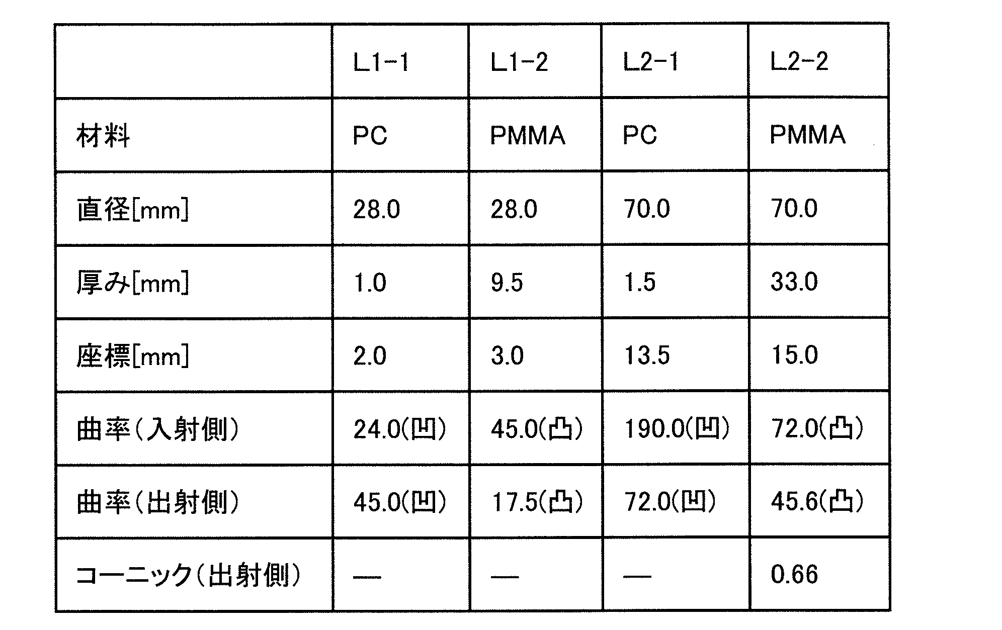
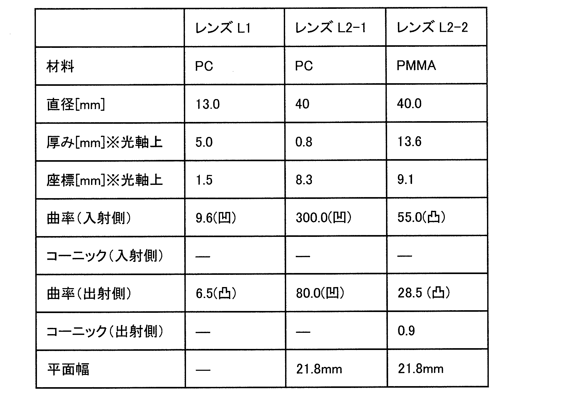
図42(a)は、本実施形態の照明装置が備える光源1の近傍を示しており、複数のLEDチップ1aを封止する封止層1bの上に、透光性を有する拡散層40aが設けられている。拡散層40aは、その表面において、典型的には不規則に配置された多数の微細な凹凸を有している。
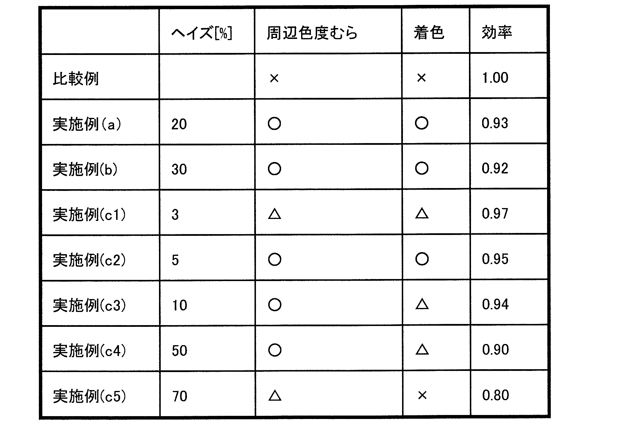
ヘイズ値(%)=(Td/Tt)×100
図43(a)はLED照明装置に用いられる一般的な光源(比較例)を示し、図43(b)~(e)は、本実施形態の照明装置で用いられる種々の光源を示す。
本実施形態では、図47に示すように、照明装置440の光出射側において遮光部材としての筒状のフード48を設ける。後述するように、照明装置440から発せられる光の配向角に応じて適切にフード48の長さLf2を調節することによって、光の利用効率を高くしたまま、照射領域周辺で発生する迷光を防止することができる。
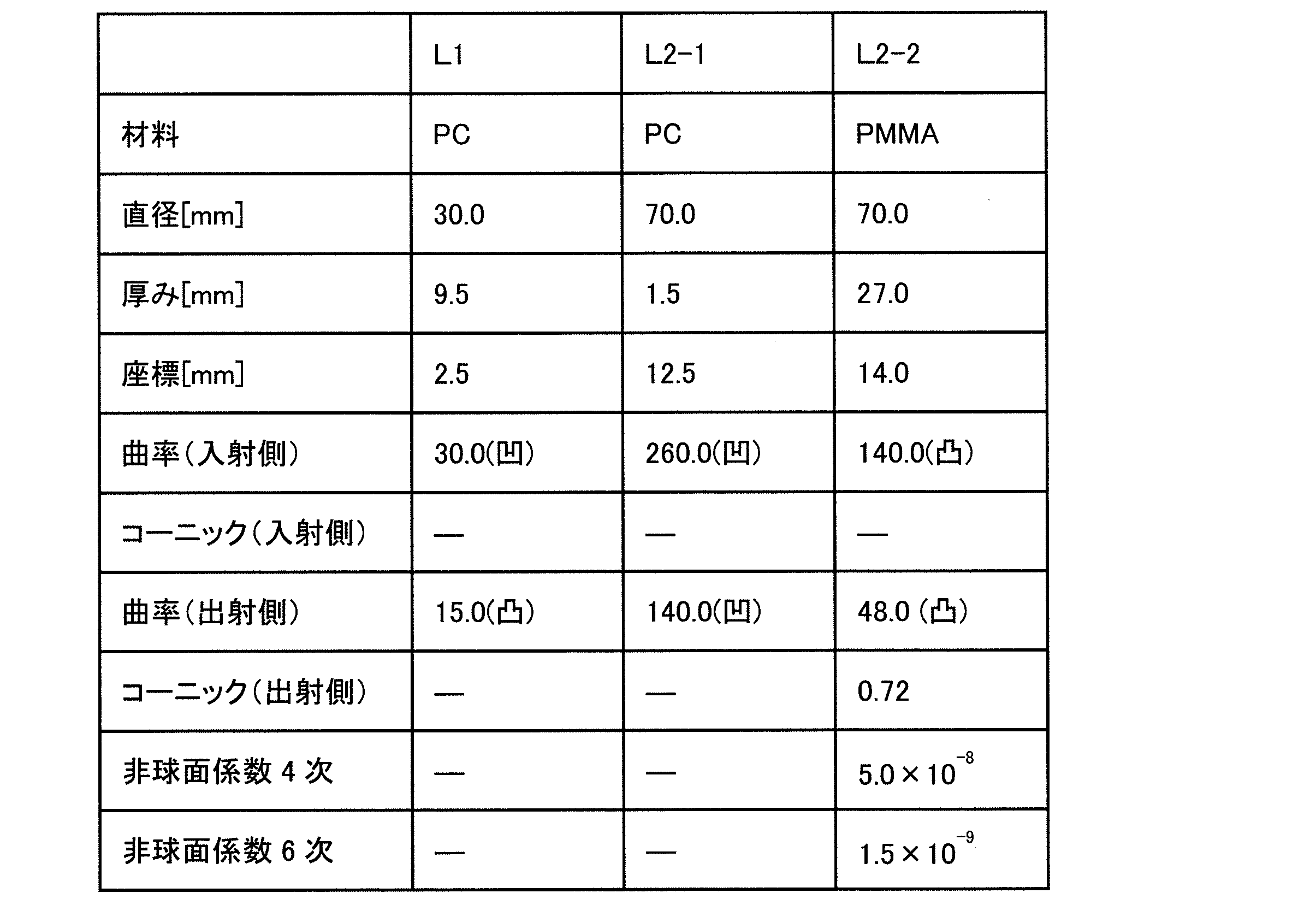
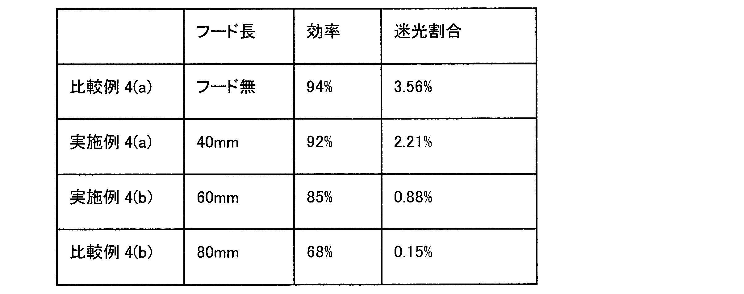
L2y=Rf/tanθ1-Lf1
L2s=Rf/tanθ2-Lf1
Rf/tanθ2-Lf1<Lf2<Rf/tanθ1-Lf1
本実施形態では、図49に示すように、照明装置450に設けられた第1レンズL1の光入射側面および/または光出射側面において、また、第2レンズL2の両側面において反射防止層50(以下、AR層50と呼ぶことがある)を設ける形態を説明する。


図50に示す本実施形態の照明装置460において、第1レンズL1および第2レンズL2のコバに吸収層Lsaが設けられている。なお、コバとは、レンズの縁の側面部分(典型的には円筒側面をなす面)を意味する。また、吸収層Lsaは、レンズのコバを黒塗りすることによって形成している。
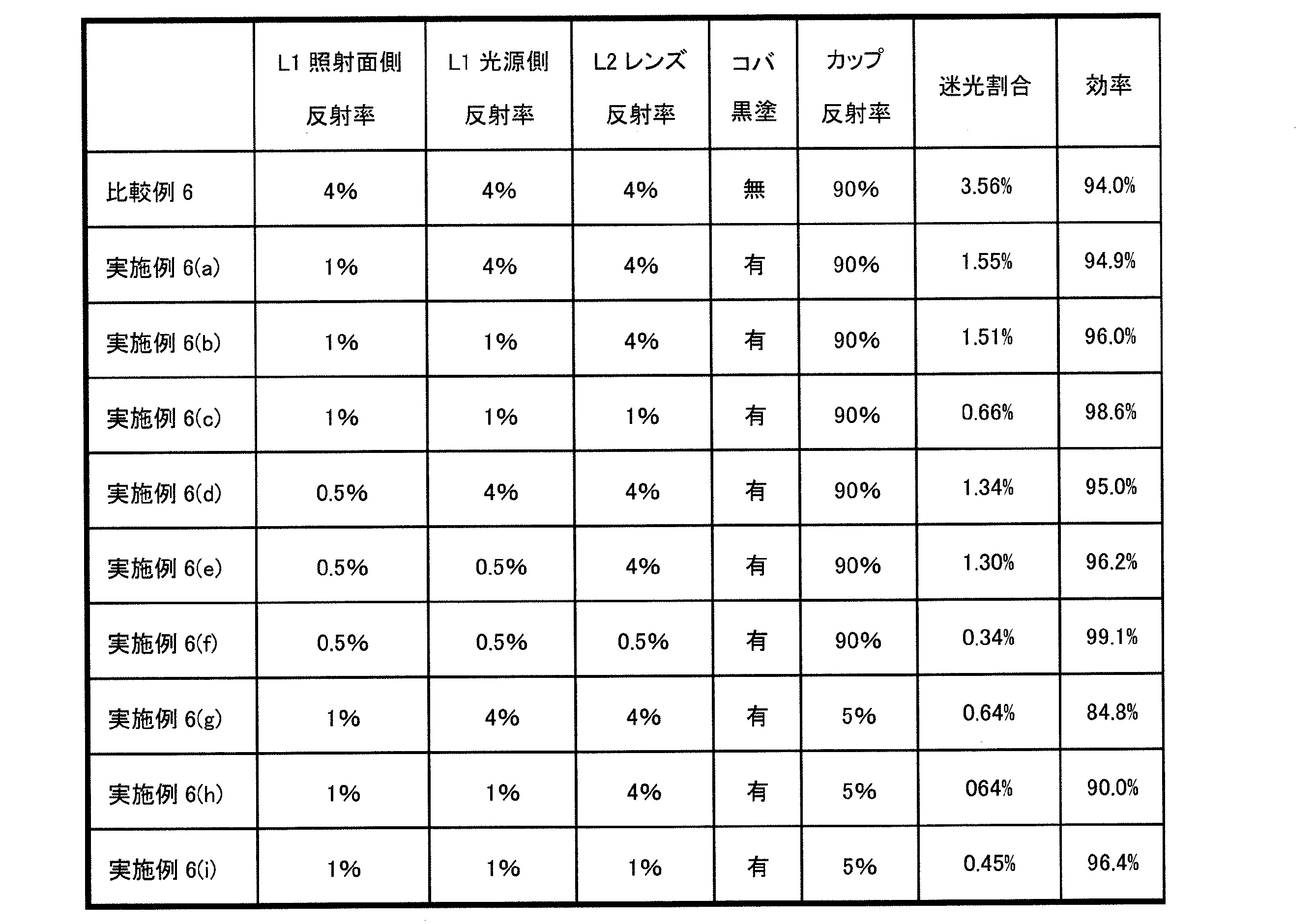

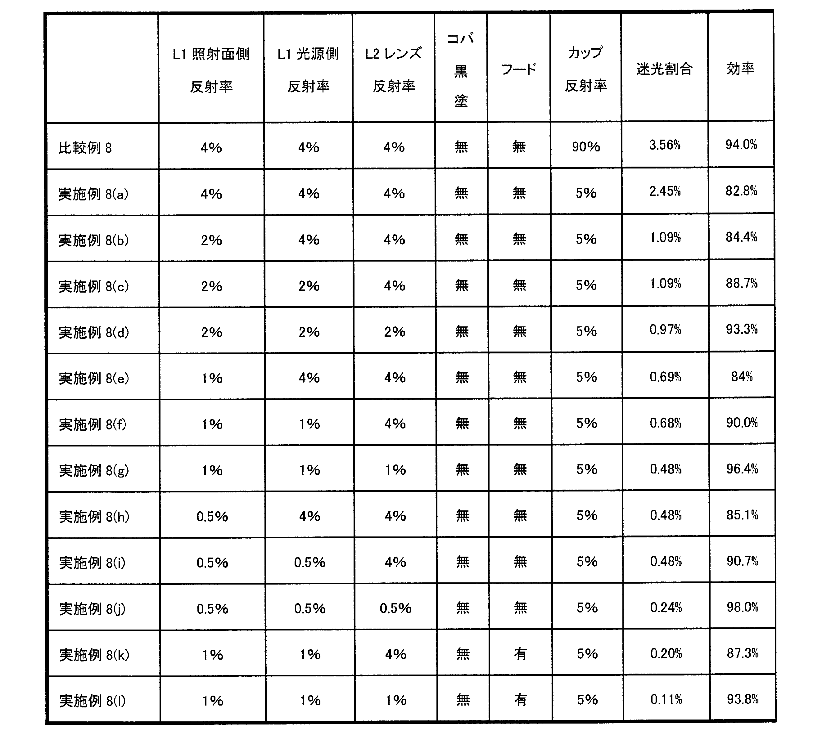
上記のように凸レンズおよびメニスカスレンズの組み合わせを用いた場合、レンズを構成する材料が適切に選択されていないと、照射エリアの端部が、中心付近と異なる色を呈する現象(色づき現象)が生じてしまう可能性があることを本発明者らは見出した。
本実施形態の照明装置は、図1に示した照明装置と同様の構成を有している。すなわち、照明装置は、図1に示すように、光源(発光部)1と、光源1の光取り出し側である、光出射面側の光軸Ax上に配置された光学レンズ部2aとを含み、光源1で発光された光を、光学レンズ部2(第1光学レンズ部)aを通して光照射するようになっている。
光源1は、面発光を行う面発光体であるLED発光体からなる。なお、面発光を行う面発光体であれば、LED発光体に限定されるものではない。例えば、発光部として蛍光体を含む発光部を用い、光源と発光部とを分離したリモートフォスファー構造を採用しても良い。なお、本実施形態のLED発光体(面発光体)の発光面の形状は矩形形状であり、この矩形の面積は6mm×6mm程度である。
光学レンズL1は、少なくとも光源1の発光面の最大幅よりも大きな直径を有しており、光源1側の面が凹面形状となった光学レンズからなる。
光学レンズL2は、少なくとも1枚目の光学レンズである光学レンズL1の最大径よりも大きな直径を有しており、光射出面側は凸形状となったレンズからなる。
また、本実施形態の照明装置は、図2に示した照明装置と同様の構成であっても良い。以下、本構成において、上記のように適切にアッベ数が選択されたレンズを用いることの利点を説明する。
図56および図57は本実施の形態に係る照明装置11cの概略構成を示す図である。
照明装置11cは、上記の光学レンズ部2aの他に、さらに2枚の照射角度調整用レンズである光学レンズL3、L4からなる光学レンズ部2bが、光学レンズ部2aの光射出側に設けられている点で、上記の照明装置11a、11bと異なっている。
光学レンズ部2bは、2枚の光学レンズL3、L4からなり、光学レンズ部2aの光出射側に近い側から順に、光学レンズL3、光学レンズL4が配置された構造となっている。なお、光学レンズL3、L4は、それぞれの中心が光軸Axを通るように配置されている。
光学レンズL3は、少なくとも光学レンズL2の光軸Axに垂直な断面(最大)の直径よりも大きな直径を有しており、光学レンズL2側の面が凹面形状となった光学レンズからなる。
光学レンズL4は、少なくとも1枚目の光学レンズである光学レンズL3の最大径よりも大きな直径を有しており、光射出面側は凸形状となったレンズからなる。
照明装置11cによれば、発光部から出射される光のほぼ全ての光を利用することができ、高い光利用効率を実現するとともに、発光部の異なる場所から出射する光をほぼ等しい照射領域へ照射することが可能となり、照射領域の均一性を飛躍的に向上させることができ、照射光の照射エリア(スポット)の中心付近と端部の色変化を小さくしながら、広角または狭角への変更が可能となる。
本発明のさらに他の実施の形態について説明すれば以下の通りである。ここでは、光学レンズ部2の2枚構成の光学レンズを一体化した例について説明する。
図60は、本実施の形態に係る照明装置11dの概略構成を示す図である。
光源1は、面発光を行う面発光体であるLED発光体からなる。なお、面発光を行う面発光体であれば、LED発光体に限定されるものではない。例えば、発光部として蛍光体を含む発光部を用い、光源と発光部とを分離した構造を採用しても良い。なお、本実施形態のLED発光体(面発光体)の発光面の形状は、略円形状であり直径は2mmΦである。
光源1の発光面に垂直な方向に射出する光は、光学レンズL2の各空気界面において、概ね垂直入射している。その為、同図に示すように、光学レンズL1、L2の各レンズの中央付近の一部を接触または接合させても、射出角度分布に大きな影響を及ぼすことなく、照射領域の均一性が実現される。
光学レンズL1は、少なくとも光源1の発光面の最大幅よりも大きな直径を有しており、光源1側の面が凹面形状となった光学レンズからなる。
光学レンズL2は、少なくとも1枚目の光学レンズである光学レンズL1の最大径よりも大きな直径を有しており、光射出面側は凸形状となったレンズからなる。
図60に示す照明装置11dでは、光学レンズL1、L2を一体成型または、光学レンズL1、L2を接合させて光学レンズ部2cとした例を示している。
(1)一体成型:具体的には、アクリル材質等の樹脂(本実施形態では、アッベ数58のPMMAを使用)を金型によって光学レンズL1、L2を一体成型して光学レンズ部2cとする。
(2)接合:一方、光源1の発光面に近いレンズ(光学レンズL1)と発光面から遠いレンズ(光学レンズL2)とをそれぞれ成型した後、各レンズの中心付近で接着させて光学レンズ部2cとしても良い。
(a)レンズ作成工程:アッベ数が54以上の透光性材料を用いて複数の光学レンズのそれぞれを作成するレンズ作成工程。
(b)接合工程:光学レンズ部2cを構成する各光学レンズのそれぞれの焦点位置が、各光学レンズによって発生するそれぞれの虚像に対して、発光部に対向する面とは反対側に存在するように、(a)のレンズ作成工程で作成した複数の光学レンズのそれぞれを、光軸調整を行って接合する。
2 光学レンズ部
3 光学レンズ
4 光学レンズ
5 開口部
11 照明装置
12 照明装置
13a 照明装置
13b 照明装置
22 光学レンズ部
23 光学レンズ部
AX 光軸
L1 光学レンズ (第1レンズ)
L2 光学レンズ (第2レンズ)
f1 第1の焦点位置
f2 第2の焦点位置
F1 第1レンズの焦点
F2 第2レンズの焦点
Claims (25)
- 光出射面を有する面光源と、
第1の焦点を有し、前記面光源の前記光出射面側に配置された第1レンズと、
第2の焦点を有し、前記第1レンズの光出射面側に配置された第2レンズと
を備え、
前記第1レンズによって第1の虚像が形成され、かつ、前記第2レンズによって第2の虚像が形成されるように、前記面光源、前記第1レンズおよび前記第2レンズが構成されている照明装置であって、
前記第2の焦点と、前記第1レンズとの間に、前記第1の虚像が形成され、
前記第2の焦点は、前記第2レンズの主点から所定焦点距離f’だけ離れた位置よりも前記面光源とは反対の側に位置しており、
前記第2レンズの主点と前記第1の虚像の位置との間の距離をl’とし、前記第2レンズの有効径をDとし、前記面光源の光出射面のサイズまたは前記面光源に含まれる複数の発光素子の配列ピッチのいずれか一方である光源サイズファクタをεとすると、
前記所定焦点距離f’は、l’=(D/(ε+D))・f’を満たす、照明装置。 - 前記第1レンズによって形成される前記第1の虚像が、前記第2レンズの焦点よりも前記面光源側に位置している、請求項1に記載の照明装置。
- 前記第1の焦点と前記第1レンズとの間に前記第1の虚像が形成され、かつ、前記第2の焦点と前記第2レンズとの間に前記第2の虚像が形成される、請求項2に記載の照明装置。
- 前記第1レンズと前記第2レンズとの合成焦点と、前記第1レンズとの間において、前記第1の虚像および前記第2の虚像が形成される、請求項3に記載の照明装置。
- 前記第1レンズと前記第2レンズとを含む第1の光学系の光出射側に、第2の光学系がさらに設けられている、請求項1から4のいずれかに記載の照明装置。
- 前記第2の光学系は、前記第1の光学系に対して最も近接する凹レンズと、前記第1の光学系に対して前記凹レンズの次に近接する凸レンズとを含む、請求項5に記載の照明装置。
- 前記第1レンズの光出射面と前記第2レンズの光入射面とが接合している、請求項1から6のいずれかに記載の照明装置。
- 前記第1レンズと前記第2レンズとは、樹脂により一体成型されている、請求項7に記載の照明装置。
- 前記第1レンズの前記面光源に対向する側のレンズ面は凹曲面であり、
光軸上における前記面光源の光出射面から前記第1レンズの凹曲面までの距離をd、前記第1レンズの前記凹曲面が有する曲率半径をRとしたとき、
前記光出射面を配置可能な位置の範囲幅hは、
h≦2√(d(2R-d))
で表される、請求項1から8のいずれかに記載の照明装置。 - 前記第1レンズおよび第2レンズを含む光学レンズ部の主点から、前記光出射面までの距離をa、前記光学レンズ部の主点から焦点位置までの距離をfとしたとき、
a<f/2
を満たす、請求項1から9のいずれかに記載の照明装置。 - 前記面光源は、互いに離間して配置された複数の発光素子を含む請求項1から10のいずれかに記載の照明装置。
- 前記第1レンズおよび前記第2レンズは、アッベ数が54以上の材料から形成されている、請求項1から11のいずれかに記載の照明装置。
- 前記第1レンズおよび前記第2レンズは、耐熱性を有する材料から形成されている請求項12に記載の照明装置。
- 前記第1レンズおよび前記第2レンズのうちの少なくとも一方は、アクロマートレンズである請求項1から13のいずれかに記載の照明装置。
- 前記アクロマートレンズは、凹レンズと前記凹レンズに密着する凸レンズとから構成されており、前記凹レンズと前記凸レンズとの中央部における接合界面が平面である、請求項14に記載の照明装置。
- 前記面光源と前記第1レンズとの間に設けられた光拡散層をさらに有する、請求項1から15のいずれかに記載の照明装置。
- 前記光拡散層のヘイズ値は、5%~50%である請求項16に記載の照明装置。
- 前記面光源は、ピッチPで並べられた複数の発光素子と、前記複数の発光素子と重なるように配置された蛍光体とを含み、前記蛍光体のエッジと、前記蛍光体のエッジに最も近い位置に配置された発光素子のエッジとの間の距離をAとしたとき、A≦Pを満たす、請求項1から17のいずれかに記載の照明装置。
- 前記第2レンズの光出射側に配置され、前記第2レンズから出射された光の一部のみを遮るように設けられたフードをさらに備える、請求項1から18のいずれかに記載の照明装置。
- 光軸上における、前記面光源の発光面の位置から前記フードの先端の位置までの距離Lf1+Lf2は、角度-相対照度グラフの傾きが-0.1よりも小さくなる最小の角度をθ1とし、迷光領域の光束/(照射領域の光束+迷光領域の光束)で表される迷光割合が1%以下となる出射角度をθ2とし、前記フードの半径をRfとしたとき、Rf/tanθ2<Lf1+Lf2<Rf/tanθ1を満たす、請求項19に記載の照明装置。
- 前記第1レンズの光出射面および光入射面ならびに前記第2レンズの光出射面および光入射面のうちの少なくとも1つにおいて反射防止層が設けられている、請求項1から20のいずれかに記載の照明装置。
- 前記第1レンズおよび前記第2レンズの少なくとも一方のコバに、光吸収層が設けられている請求項1から21のいずれかに記載の照明装置。
- 前記面光源、前記第1レンズおよび前記第2レンズを収容する空間を有する筺体をさらに備え、前記収容する空間の外側を規定する筺体部分の少なくとも一部において光吸収層が設けられている請求項1から22のいずれかに記載の照明装置。
- 請求項1から23のいずれかに記載の照明装置をヘッドライトとして用いた自動車。
- スクリーン上に光を照射したときに得られる照射角度-相対照度グラフにおいて、相対照度0.10となる点の接線と照射角度を示す軸との交点よりも内側の領域を照射領域とし、前記照射領域の外側の領域を迷光領域としたときに、迷光領域の光束/(照射領域の光束+迷光領域の光束)によって表される迷光割合が3%以下である照明装置。
Priority Applications (3)
| Application Number | Priority Date | Filing Date | Title |
|---|---|---|---|
| CN201380040036.6A CN104662357B (zh) | 2012-07-27 | 2013-07-26 | 照明装置 |
| JP2014527038A JP5901037B2 (ja) | 2012-07-27 | 2013-07-26 | 照明装置 |
| US14/417,254 US9939127B2 (en) | 2012-07-27 | 2013-07-26 | Illumination device |
Applications Claiming Priority (4)
| Application Number | Priority Date | Filing Date | Title |
|---|---|---|---|
| JP2012167663 | 2012-07-27 | ||
| JP2012-167663 | 2012-07-27 | ||
| PCT/JP2013/068124 WO2014017262A1 (ja) | 2012-07-27 | 2013-07-02 | 照明装置 |
| JPPCT/JP2013/068124 | 2013-07-02 |
Publications (1)
| Publication Number | Publication Date |
|---|---|
| WO2014017652A1 true WO2014017652A1 (ja) | 2014-01-30 |
Family
ID=49997078
Family Applications (2)
| Application Number | Title | Priority Date | Filing Date |
|---|---|---|---|
| PCT/JP2013/068124 Ceased WO2014017262A1 (ja) | 2012-07-27 | 2013-07-02 | 照明装置 |
| PCT/JP2013/070379 Ceased WO2014017652A1 (ja) | 2012-07-27 | 2013-07-26 | 照明装置 |
Family Applications Before (1)
| Application Number | Title | Priority Date | Filing Date |
|---|---|---|---|
| PCT/JP2013/068124 Ceased WO2014017262A1 (ja) | 2012-07-27 | 2013-07-02 | 照明装置 |
Country Status (4)
| Country | Link |
|---|---|
| US (2) | US9217552B2 (ja) |
| JP (2) | JP5901036B2 (ja) |
| CN (2) | CN104508356B (ja) |
| WO (2) | WO2014017262A1 (ja) |
Cited By (10)
| Publication number | Priority date | Publication date | Assignee | Title |
|---|---|---|---|---|
| JP2015179897A (ja) * | 2014-03-18 | 2015-10-08 | 富士ゼロックス株式会社 | 照明装置および画像読取装置、画像形成装置 |
| WO2016186179A1 (ja) * | 2015-05-21 | 2016-11-24 | 市光工業株式会社 | 車両用灯具 |
| WO2017002725A1 (ja) * | 2015-07-02 | 2017-01-05 | 株式会社エンプラス | 発光装置、面光源装置および表示装置 |
| JP2017016995A (ja) * | 2015-07-02 | 2017-01-19 | 株式会社エンプラス | 発光装置、面光源装置および表示装置 |
| JP2017054708A (ja) * | 2015-09-10 | 2017-03-16 | 株式会社東芝 | Led照明装置 |
| KR20170098713A (ko) * | 2016-02-22 | 2017-08-30 | 발레오 비젼 | 광원의 매트릭스를 구비하는 광빔 투사 장치 및 이러한 장치를 구비한 헤드라이트 모듈 |
| KR20190081639A (ko) * | 2017-12-29 | 2019-07-09 | 에스엘 주식회사 | 차량용 광학계 및 이를 이용한 차량용 램프 |
| JP2020507110A (ja) * | 2017-01-17 | 2020-03-05 | シグニファイ ホールディング ビー ヴィSignify Holding B.V. | 調節可能なスポットライト位置生成 |
| WO2021149372A1 (ja) * | 2020-01-20 | 2021-07-29 | ソニーセミコンダクタソリューションズ株式会社 | 発光装置およびその製造方法 |
| JP2026002974A (ja) * | 2019-09-25 | 2026-01-08 | パナソニックIpマネジメント株式会社 | 照明装置 |
Families Citing this family (28)
| Publication number | Priority date | Publication date | Assignee | Title |
|---|---|---|---|---|
| US9217552B2 (en) * | 2012-07-27 | 2015-12-22 | Sharp Kabushiki Kaisha | Illumination device |
| KR20170041359A (ko) * | 2015-10-07 | 2017-04-17 | 엘지이노텍 주식회사 | 조명 장치 |
| JP6746896B2 (ja) * | 2015-11-10 | 2020-08-26 | 市光工業株式会社 | 車両用灯具 |
| CN106907593A (zh) * | 2015-12-23 | 2017-06-30 | 欧普照明股份有限公司 | 一种光学装置和照明装置 |
| FR3047794B1 (fr) * | 2016-02-16 | 2018-03-09 | Valeo Vision | Systeme de lentilles de projection d'au moins une source lumineuse |
| JP6805706B2 (ja) * | 2016-10-12 | 2020-12-23 | 市光工業株式会社 | 車両用灯具 |
| KR102482762B1 (ko) * | 2017-01-10 | 2022-12-29 | 서울바이오시스 주식회사 | 포충기 |
| CN107166213A (zh) * | 2017-05-02 | 2017-09-15 | 曹云东 | Uvled光的汇聚方法 |
| FR3068435B1 (fr) * | 2017-06-29 | 2019-11-29 | Valeo Vision | Module lumineux comportant un element optique de correction de champ |
| DE102018112453A1 (de) * | 2018-05-24 | 2019-11-28 | HELLA GmbH & Co. KGaA | Vorfeldlichtmodul |
| WO2020035894A1 (ja) * | 2018-08-13 | 2020-02-20 | スタンレー電気株式会社 | 照明光学系 |
| DE102018213926A1 (de) * | 2018-08-17 | 2020-02-20 | Koninklijke Philips N.V. | Optische Linse für eine photodiodenbestückte Vorrichtung |
| CN112955805B (zh) * | 2018-10-04 | 2023-08-01 | 幹太向·牛方株式会社 | 光学系统装置及双凸透镜 |
| JP7190647B2 (ja) * | 2018-11-08 | 2022-12-16 | パナソニックIpマネジメント株式会社 | 照明器具 |
| IT201900004783A1 (it) * | 2019-03-29 | 2020-09-29 | Coelux Srl | Generatore di luce diretta per sistemi di illuminazione a imitazione cielo - sole |
| CN210740254U (zh) | 2019-06-05 | 2020-06-12 | 华域视觉科技(上海)有限公司 | 车灯光学元件、车灯模组、车辆前照灯及车辆 |
| CN112666679B (zh) * | 2019-10-16 | 2022-03-18 | 比亚迪股份有限公司 | 移动通信设备的摄像头模组和具有其的移动通信设备 |
| US11318882B2 (en) | 2020-03-19 | 2022-05-03 | B/E Aerospace, Inc. | Color correction method for chromatic aberration using multiple color LED sources |
| CN112013301A (zh) * | 2020-08-24 | 2020-12-01 | 杭州星野光学科技有限公司 | 一种壁挂灯 |
| KR102427239B1 (ko) * | 2020-10-22 | 2022-08-22 | (주)아덴하이진 | 인체무해 uv광원을 이용한 살균장치 |
| US12164194B2 (en) | 2022-01-11 | 2024-12-10 | Hefei Raysees Ai Technology Co., Ltd. | Backlight module and display device |
| US12055813B2 (en) | 2022-02-22 | 2024-08-06 | Hefei Raysees Ai Technology Co., Ltd. | Backlight module and display device |
| US12529930B2 (en) | 2022-10-31 | 2026-01-20 | Hefei Raysees Ai Technology Co., Ltd. | Backlight module and display device |
| CN116085723B (zh) * | 2023-02-13 | 2025-12-19 | 浙江大华技术股份有限公司 | 一种补光透镜及补光透镜的设计方法 |
| CN116146930B (zh) * | 2023-03-01 | 2026-03-06 | 曼德电子电器有限公司 | 光学透镜模组及车灯 |
| FI131762B1 (en) * | 2023-09-26 | 2025-11-17 | Ledil Oy | Optical system for modifying light distribution |
| EP4707879A1 (en) * | 2024-09-05 | 2026-03-11 | Stryker Corporation | Aspheric lenses and optical assemblies for generating uniform rectangular irradiance distributions |
| CN119937230B (zh) * | 2025-03-05 | 2025-11-11 | 西安通立软件开发有限公司 | 投影光学结构、投影光学镜面调整方法及投影镜头 |
Citations (3)
| Publication number | Priority date | Publication date | Assignee | Title |
|---|---|---|---|---|
| JP3148803U (ja) * | 2008-06-30 | 2009-03-05 | 一品光学工業股▲ふん▼有限公司 | 非球面正照射角度発光ダイオードの光学レンズ及びそれを構成する発光ダイオード構成部材 |
| JP2010085493A (ja) * | 2008-09-29 | 2010-04-15 | Asahi Rubber Inc | レンズ及びそれを用いた光学製品 |
| JP2011505599A (ja) * | 2007-12-03 | 2011-02-24 | デジスライド ホールディングス リミテッド | Led配列及びダイクロイックウェッジを使用する小型投射装置 |
Family Cites Families (30)
| Publication number | Priority date | Publication date | Assignee | Title |
|---|---|---|---|---|
| DE3516812A1 (de) * | 1985-05-10 | 1986-11-13 | Hella KG Hueck & Co, 4780 Lippstadt | Abgeblendeter fahrzeugscheinwerfer |
| TW512214B (en) * | 2000-01-07 | 2002-12-01 | Koninkl Philips Electronics Nv | Luminaire |
| DE10046840A1 (de) * | 2000-09-20 | 2002-07-04 | Goodrich Hella Aerospace Ls | Leseleuchte für einen Fahrzeuginnenraum |
| US20040190286A1 (en) * | 2003-03-25 | 2004-09-30 | Chapman Leonard T. | Flashlight |
| US20060139580A1 (en) * | 2004-12-29 | 2006-06-29 | Conner Arlie R | Illumination system using multiple light sources with integrating tunnel and projection systems using same |
| CN2829103Y (zh) * | 2005-05-09 | 2006-10-18 | 葛世潮 | 高效率发光二极管 |
| US7175299B2 (en) | 2005-05-10 | 2007-02-13 | Alan Uke | Multi-lens zoom system and method for flashlights |
| DE102006045446B4 (de) * | 2005-09-26 | 2017-05-24 | Stanley Electric Co. Ltd. | Fahrzeugleuchte |
| US7798678B2 (en) | 2005-12-30 | 2010-09-21 | 3M Innovative Properties Company | LED with compound encapsulant lens |
| KR101445404B1 (ko) | 2006-07-31 | 2014-09-26 | 쓰리엠 이노베이티브 프로퍼티즈 컴파니 | 중공 집광 렌즈를 갖는 led 광원 |
| TWI299311B (en) * | 2006-09-27 | 2008-08-01 | Ind Tech Res Inst | Illuminating device |
| JP2009004276A (ja) | 2007-06-22 | 2009-01-08 | Toshiba Lighting & Technology Corp | スポットライト |
| US8845109B2 (en) * | 2007-11-24 | 2014-09-30 | Yong-Jing Wang | Projection system based on self emitting display panel |
| CN101515064A (zh) * | 2008-02-19 | 2009-08-26 | 台湾基材科技股份有限公司 | 集光装置 |
| TWI355520B (en) * | 2008-08-21 | 2012-01-01 | All Real Technology Co Ltd | Artificial light source generator |
| TW201030281A (en) * | 2009-02-13 | 2010-08-16 | Ama Precision Inc | Light-emitting apparatus and light-guiding member thereof |
| US8408772B2 (en) * | 2009-02-13 | 2013-04-02 | Excelitas Technologies LED Solutions, Inc. | LED illumination device |
| US8047684B2 (en) * | 2009-11-23 | 2011-11-01 | General Scientific Corporation | LED illuminator with improved beam quality |
| US8419188B2 (en) * | 2010-04-07 | 2013-04-16 | Microvision, Inc. | Dichroic wedge stack light combining apparatus, system and method |
| JP5010010B2 (ja) * | 2010-04-16 | 2012-08-29 | フェニックス電機株式会社 | 発光装置 |
| CN102410492A (zh) * | 2010-09-21 | 2012-04-11 | 富士迈半导体精密工业(上海)有限公司 | 透镜及发光二极管模组 |
| US8899792B2 (en) * | 2010-09-24 | 2014-12-02 | Illumitex, Inc. | High NA optical system and device |
| TWI425295B (zh) * | 2010-09-28 | 2014-02-01 | 台達電子工業股份有限公司 | 光源系統與投影裝置 |
| CN102081280B (zh) * | 2010-12-03 | 2012-09-05 | 深圳中兴力维技术有限公司 | 一种变焦式红外灯及其控制方法、红外摄像机 |
| WO2012121715A1 (en) * | 2011-03-09 | 2012-09-13 | Empire Technology Development Llc | Shading system using liquid lens and light waveguide |
| TW201248204A (en) * | 2011-05-26 | 2012-12-01 | Asia Vital Components Co Ltd | Optical lens and lighting device |
| CN202125883U (zh) * | 2011-06-08 | 2012-01-25 | 杭州瑾丽光电科技有限公司 | 双聚光镜加成像物镜的照明装置 |
| CN102506365B (zh) * | 2011-10-19 | 2014-06-18 | 上海英汇科技发展有限公司 | 一种车门投影灯及其应用 |
| JP5292657B2 (ja) * | 2012-02-17 | 2013-09-18 | スタンレー電気株式会社 | 車両用ランプ |
| US9217552B2 (en) * | 2012-07-27 | 2015-12-22 | Sharp Kabushiki Kaisha | Illumination device |
-
2013
- 2013-07-02 US US14/417,235 patent/US9217552B2/en not_active Expired - Fee Related
- 2013-07-02 JP JP2014526835A patent/JP5901036B2/ja not_active Expired - Fee Related
- 2013-07-02 WO PCT/JP2013/068124 patent/WO2014017262A1/ja not_active Ceased
- 2013-07-02 CN CN201380039908.7A patent/CN104508356B/zh not_active Expired - Fee Related
- 2013-07-26 US US14/417,254 patent/US9939127B2/en active Active
- 2013-07-26 WO PCT/JP2013/070379 patent/WO2014017652A1/ja not_active Ceased
- 2013-07-26 CN CN201380040036.6A patent/CN104662357B/zh not_active Expired - Fee Related
- 2013-07-26 JP JP2014527038A patent/JP5901037B2/ja not_active Expired - Fee Related
Patent Citations (3)
| Publication number | Priority date | Publication date | Assignee | Title |
|---|---|---|---|---|
| JP2011505599A (ja) * | 2007-12-03 | 2011-02-24 | デジスライド ホールディングス リミテッド | Led配列及びダイクロイックウェッジを使用する小型投射装置 |
| JP3148803U (ja) * | 2008-06-30 | 2009-03-05 | 一品光学工業股▲ふん▼有限公司 | 非球面正照射角度発光ダイオードの光学レンズ及びそれを構成する発光ダイオード構成部材 |
| JP2010085493A (ja) * | 2008-09-29 | 2010-04-15 | Asahi Rubber Inc | レンズ及びそれを用いた光学製品 |
Cited By (18)
| Publication number | Priority date | Publication date | Assignee | Title |
|---|---|---|---|---|
| JP2015179897A (ja) * | 2014-03-18 | 2015-10-08 | 富士ゼロックス株式会社 | 照明装置および画像読取装置、画像形成装置 |
| EP3299698A4 (en) * | 2015-05-21 | 2019-01-23 | Ichikoh Industries, Ltd. | VEHICLE LAMP |
| WO2016186179A1 (ja) * | 2015-05-21 | 2016-11-24 | 市光工業株式会社 | 車両用灯具 |
| JP2016219282A (ja) * | 2015-05-21 | 2016-12-22 | 市光工業株式会社 | 車両用灯具 |
| US10295138B2 (en) | 2015-05-21 | 2019-05-21 | Ichikoh Industries, Ltd. | Vehicle lamp |
| JP2017016995A (ja) * | 2015-07-02 | 2017-01-19 | 株式会社エンプラス | 発光装置、面光源装置および表示装置 |
| WO2017002725A1 (ja) * | 2015-07-02 | 2017-01-05 | 株式会社エンプラス | 発光装置、面光源装置および表示装置 |
| US10323804B2 (en) | 2015-07-02 | 2019-06-18 | Enplas Corporation | Light-emitting device, surface light source device and display device |
| JP2017054708A (ja) * | 2015-09-10 | 2017-03-16 | 株式会社東芝 | Led照明装置 |
| KR20170098713A (ko) * | 2016-02-22 | 2017-08-30 | 발레오 비젼 | 광원의 매트릭스를 구비하는 광빔 투사 장치 및 이러한 장치를 구비한 헤드라이트 모듈 |
| JP2017162800A (ja) * | 2016-02-22 | 2017-09-14 | ヴァレオ ビジョンValeo Vision | 光源のマトリックスを備えた光ビーム投影デバイス、当該デバイスを備えた照明およびヘッドライトモジュール |
| KR102677698B1 (ko) | 2016-02-22 | 2024-06-21 | 발레오 비젼 | 광원의 매트릭스를 구비하는 광빔 투사 장치 및 이러한 장치를 구비한 헤드라이트 모듈 |
| JP2020507110A (ja) * | 2017-01-17 | 2020-03-05 | シグニファイ ホールディング ビー ヴィSignify Holding B.V. | 調節可能なスポットライト位置生成 |
| JP7002552B2 (ja) | 2017-01-17 | 2022-02-04 | シグニファイ ホールディング ビー ヴィ | 調節可能なスポットライト位置生成 |
| KR20190081639A (ko) * | 2017-12-29 | 2019-07-09 | 에스엘 주식회사 | 차량용 광학계 및 이를 이용한 차량용 램프 |
| KR102495169B1 (ko) | 2017-12-29 | 2023-02-03 | 에스엘 주식회사 | 차량용 광학계 및 이를 이용한 차량용 램프 |
| JP2026002974A (ja) * | 2019-09-25 | 2026-01-08 | パナソニックIpマネジメント株式会社 | 照明装置 |
| WO2021149372A1 (ja) * | 2020-01-20 | 2021-07-29 | ソニーセミコンダクタソリューションズ株式会社 | 発光装置およびその製造方法 |
Also Published As
| Publication number | Publication date |
|---|---|
| CN104508356B (zh) | 2016-09-28 |
| CN104508356A (zh) | 2015-04-08 |
| US20150211709A1 (en) | 2015-07-30 |
| WO2014017262A1 (ja) | 2014-01-30 |
| US9939127B2 (en) | 2018-04-10 |
| CN104662357A (zh) | 2015-05-27 |
| JPWO2014017262A1 (ja) | 2016-07-07 |
| JP5901037B2 (ja) | 2016-04-06 |
| US20150167924A1 (en) | 2015-06-18 |
| JP5901036B2 (ja) | 2016-04-06 |
| CN104662357B (zh) | 2016-06-22 |
| US9217552B2 (en) | 2015-12-22 |
| JPWO2014017652A1 (ja) | 2016-07-11 |
Similar Documents
| Publication | Publication Date | Title |
|---|---|---|
| JP5901037B2 (ja) | 照明装置 | |
| US10295153B2 (en) | Optical system for producing uniform illumination | |
| US8899792B2 (en) | High NA optical system and device | |
| KR20140137358A (ko) | 단초점 조명을 위한 조명 렌즈 | |
| JP2010500710A (ja) | 光源及び光ガイドを有すること照明装置 | |
| KR20150012260A (ko) | 광학 소자 | |
| WO2018061534A1 (ja) | 導光部材、導光部材ユニットおよび照明装置 | |
| EP2841974B1 (en) | Color correcting optical element | |
| US8403538B2 (en) | Color homogenizing optical assembly | |
| US9890919B2 (en) | Lamp lens with reduced chromatic aberration and lamp for vehicle using the same | |
| TWM540240U (zh) | 可消除色散的直射式led照明模組 | |
| JP2013251105A (ja) | 照明用レンズおよび照明装置 | |
| JP2013214449A (ja) | トロイダルレンズおよび照明装置 | |
| US20200041098A1 (en) | Collimator and a lighting unit | |
| CN116888402A (zh) | 用于可转向反射照明器的光学设计 | |
| US10794565B2 (en) | Dielectric collimator with a rejecting center lens | |
| JPWO2019009405A1 (ja) | 照明装置 | |
| JP6816886B2 (ja) | 照明装置 | |
| KR102419044B1 (ko) | 광원 모듈 | |
| TWI829447B (zh) | 投影裝置 | |
| JP5315505B2 (ja) | 車両用灯具及びその製造方法 | |
| JP7287668B2 (ja) | 照明装置 | |
| TWI731332B (zh) | 投影裝置及其製造方法 | |
| JP2026008991A (ja) | 照明装置 | |
| CN117806106A (zh) | 光源组件及投影装置 |
Legal Events
| Date | Code | Title | Description |
|---|---|---|---|
| 121 | Ep: the epo has been informed by wipo that ep was designated in this application |
Ref document number: 13823129 Country of ref document: EP Kind code of ref document: A1 |
|
| ENP | Entry into the national phase |
Ref document number: 2014527038 Country of ref document: JP Kind code of ref document: A |
|
| WWE | Wipo information: entry into national phase |
Ref document number: 14417254 Country of ref document: US |
|
| NENP | Non-entry into the national phase |
Ref country code: DE |
|
| 122 | Ep: pct application non-entry in european phase |
Ref document number: 13823129 Country of ref document: EP Kind code of ref document: A1 |