WO2014017264A1 - 検査装置 - Google Patents
検査装置 Download PDFInfo
- Publication number
- WO2014017264A1 WO2014017264A1 PCT/JP2013/068200 JP2013068200W WO2014017264A1 WO 2014017264 A1 WO2014017264 A1 WO 2014017264A1 JP 2013068200 W JP2013068200 W JP 2013068200W WO 2014017264 A1 WO2014017264 A1 WO 2014017264A1
- Authority
- WO
- WIPO (PCT)
- Prior art keywords
- substrate
- inspection apparatus
- chamber
- wafer
- medium
- Prior art date
- Legal status (The legal status is an assumption and is not a legal conclusion. Google has not performed a legal analysis and makes no representation as to the accuracy of the status listed.)
- Ceased
Links
Images





Classifications
-
- G—PHYSICS
- G01—MEASURING; TESTING
- G01N—INVESTIGATING OR ANALYSING MATERIALS BY DETERMINING THEIR CHEMICAL OR PHYSICAL PROPERTIES
- G01N21/00—Investigating or analysing materials by the use of optical means, i.e. using sub-millimetre waves, infrared, visible or ultraviolet light
- G01N21/84—Systems specially adapted for particular applications
- G01N21/88—Investigating the presence of flaws or contamination
- G01N21/95—Investigating the presence of flaws or contamination characterised by the material or shape of the object to be examined
- G01N21/9501—Semiconductor wafers
-
- G—PHYSICS
- G01—MEASURING; TESTING
- G01N—INVESTIGATING OR ANALYSING MATERIALS BY DETERMINING THEIR CHEMICAL OR PHYSICAL PROPERTIES
- G01N21/00—Investigating or analysing materials by the use of optical means, i.e. using sub-millimetre waves, infrared, visible or ultraviolet light
- G01N21/01—Arrangements or apparatus for facilitating the optical investigation
-
- G—PHYSICS
- G01—MEASURING; TESTING
- G01N—INVESTIGATING OR ANALYSING MATERIALS BY DETERMINING THEIR CHEMICAL OR PHYSICAL PROPERTIES
- G01N21/00—Investigating or analysing materials by the use of optical means, i.e. using sub-millimetre waves, infrared, visible or ultraviolet light
- G01N21/84—Systems specially adapted for particular applications
- G01N21/88—Investigating the presence of flaws or contamination
-
- G—PHYSICS
- G01—MEASURING; TESTING
- G01N—INVESTIGATING OR ANALYSING MATERIALS BY DETERMINING THEIR CHEMICAL OR PHYSICAL PROPERTIES
- G01N21/00—Investigating or analysing materials by the use of optical means, i.e. using sub-millimetre waves, infrared, visible or ultraviolet light
- G01N21/84—Systems specially adapted for particular applications
- G01N21/88—Investigating the presence of flaws or contamination
- G01N21/94—Investigating contamination, e.g. dust
-
- H—ELECTRICITY
- H10—SEMICONDUCTOR DEVICES; ELECTRIC SOLID-STATE DEVICES NOT OTHERWISE PROVIDED FOR
- H10P—GENERIC PROCESSES OR APPARATUS FOR THE MANUFACTURE OR TREATMENT OF DEVICES COVERED BY CLASS H10
- H10P72/00—Handling or holding of wafers, substrates or devices during manufacture or treatment thereof
- H10P72/06—Apparatus for monitoring, sorting, marking, testing or measuring
- H10P72/0616—Monitoring of warpages, curvatures, damages, defects or the like
-
- H—ELECTRICITY
- H10—SEMICONDUCTOR DEVICES; ELECTRIC SOLID-STATE DEVICES NOT OTHERWISE PROVIDED FOR
- H10P—GENERIC PROCESSES OR APPARATUS FOR THE MANUFACTURE OR TREATMENT OF DEVICES COVERED BY CLASS H10
- H10P74/00—Testing or measuring during manufacture or treatment of wafers, substrates or devices
- H10P74/27—Structural arrangements therefor
-
- G—PHYSICS
- G01—MEASURING; TESTING
- G01N—INVESTIGATING OR ANALYSING MATERIALS BY DETERMINING THEIR CHEMICAL OR PHYSICAL PROPERTIES
- G01N2201/00—Features of devices classified in G01N21/00
- G01N2201/06—Illumination; Optics
- G01N2201/063—Illuminating optical parts
Definitions
- defects such as foreign matter and scratches on the surface of a semiconductor substrate (wafer) can cause defects such as wiring insulation defects and short circuits on the wafer, resulting in capacitor insulation defects and gate oxide film breakdown. It becomes the cause of. Therefore, it is important to detect defects on the wafer surface in the semiconductor manufacturing process and feed back to the semiconductor manufacturing process.
- An example of the inspection apparatus is an optical inspection apparatus that detects a defect on the substrate by irradiating the substrate with light and detecting the scattered light.
- Optical inspection apparatuses are roughly classified into a surface inspection apparatus that inspects a specular wafer and a wafer inspection apparatus with a pattern that inspects a wafer on which a circuit pattern is formed.
- the present invention it is possible to reduce the number of foreign substances adhering to the substrate as compared with the conventional case.
- FIG. 1 is a diagram illustrating an inspection apparatus according to Embodiment 1.
- FIG. 6 is a flowchart for explaining an inspection operation according to the first embodiment.
- FIG. 6 is a diagram illustrating a second embodiment.
- FIG. 7 is a diagram for explaining Example 2 (continuation).
- the figure explaining the chamber 201 which has the opening 801 on the side surface.
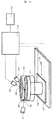
- the substrate 103 is mounted on the substrate mounting device 104.
- the substrate mounting device 104 may be a back surface adsorption method that adsorbs the entire back surface of the substrate 103, or may be a so-called edge grip method that grasps only the end portion of the substrate 103 without adsorbing the back surface.
- the substrate mounting device 104 is mounted on a spindle 106 that rotates the substrate mounting device 104. When the spindle 106 rotates, the substrate 103 also rotates.
- the spindle 106 is mounted on a stage 107 that can move in the XY direction or the X direction and can move up and down in the Z direction.
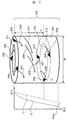
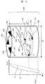
- a chamber system 105 that covers at least the substrate 103 is provided. Details of the chamber system 105 will be described with reference to FIG. FIG. 2 is a diagram for explaining the details of the chamber system 105.
- the chamber system 105 includes a chamber portion that covers at least the substrate 105, a supply system that supplies a medium such as a gas, and a discharge system that discharges the supplied medium.
- the chamber portion is expressed as a chamber 201.
- the chamber 201 covers at least the substrate 103, and has a substantially cylindrical shape.
- An opening 211 is formed in the upper part of the chamber 201.
- the illumination light 102 from the illumination optical system 101 is supplied to the substrate 103 through the opening 211, and the scattered light 108 is also detected by the detection optical systems 109 and 110 through the opening 211.
- the upper surface of the chamber 201 may be formed of an optically transparent material instead of the opening 211.
- the size of the chamber system 105 may be determined by the required cleanliness and the size of the substrate 103. Therefore, when the required size of the chamber system 105 is large, the chamber system 105 may include an illumination optical system 101 and detection optical systems 109 and 110 as shown in FIG. Further, the chamber system 105 may not be formed with the opening 211.
- a guide may be provided on the inner surface of the chamber 201 in order to reduce friction of airflows 205, 206, and 207 described later.
- protrusions or the like may be disposed on the inner surface of the chamber 201 to reduce friction of airflows 205, 206, and 207, which will be described later, and substantial unevenness may be formed.
- the inner surface of the chamber 201 may be substantially flat.
- the airflow supply units 202, 203, and 204 supply a medium such as gas into the chamber 201.
- the gas to be supplied includes air, and may be an inert gas such as nitrogen or argon.
- the gas supplied from the airflow supply units 202, 203, and 204 is represented as airflows 205, 206, and 207 in FIGS.
- the airflows 205, 206, and 207 descend spirally while forming independent laminar flows along the side surfaces of the chamber 201, and the outer periphery of the substrate 103 from above. Supplied to.
- the outer peripheral portion can be expressed in various ways. For example, it can be expressed as a place closer to the end portion of the substrate 103 than the center of the substrate 103. At this time, the paths of the airflows 205, 206, and 207 do not overlap each other, that is, no turbulent flow is generated, and different laminar flows are formed and supplied to the substrate 103.
- protrusions and the like may be arranged to form substantial unevenness.
- the surface of the shielding plate 212 may be substantially flat.
- the relationship between the height direction of the substrate 103 and the pressure in the chamber 201 is expressed as a linear function f 1 in FIGS.
- the pressure in the chamber 201 becomes higher as it goes to the upper side of the chamber 201 and lower as it goes to the lower part of the chamber 201 by supplying the airflows 205, 206, and 207.
- the minimum pressure value Pmin is controlled to be higher than the outside of the chamber 201. By setting in this way, the inflow of air from the outside can be prevented.
- the linear function f 1 not the linear function f 1 but a function f 2 having a higher order than the linear function may be used.
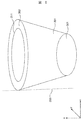
- the shape of the chamber 201 may be a substantially conical shape.
- the side surface of the chamber is inclined with respect to the normal line 303 of the substrate 103.
- the shape of the chamber 201 is a substantially conical shape, the flow rates of the airflows 205, 206, and 207 when supplied to the outer peripheral portion of the substrate 103 can be improved.
- the opening 211 may not be formed in the chamber 201 of FIG.
- the illumination light 102 is obliquely incident on the substrate 103 with a certain incident angle.
- the incident angle is substantially a Brewster angle.
- the height H of the chamber 201 is a height that can illuminate the illumination light 102 onto the substrate 103 with a Brewster angle.
- the Brewster angle is a function of the refractive index on the incident side and the refractive index on the transmission side.
- an inert gas such as nitrogen or argon can be considered in addition to air as the gas to be supplied.
- the substrate 103 to be inspected may be a so-called mirror wafer, or some film may be formed on the mirror wafer.
- the height H of the chamber 201 is changed according to the change in the Brewster angle by using changing means (for example, a combination of a rail and a block) that changes the relative distance between the substrate 103 and the chamber 201. It is good also as a structure which changes.
- at least one of the flow rate and the flow rate of the gas to be supplied may be changed according to the change in the height of the chamber 201.
- FIG. 7A is a diagram for explaining the details of the air flow supply unit 202 and the air flow exhaust unit 210
- FIG. 7B shows the air flow supply unit 202 and the air flow exhaust unit 210 from the AA ′ cross section of the chamber 201.
- FIG. 7A When observed from above the substrate 103, the air flow supply units 202, 203, and 204 are disposed so as to surround the substrate 103. The same applies to the airflow exhaust unit 210.
- the air outlets of the airflow supply units 202, 203, and 204 face the circumferential direction of the substrate. The same applies to the exhaust port of the airflow exhaust unit 210.
- the airflow supply unit 202 includes a gas supply unit 401 and a duct 402 that is a supply port.
- the gas supply unit 401 includes a gas source 4011 that supplies air, nitrogen, argon, and the like, a control unit 4012 that controls at least one of the gas flow rate and flow velocity, a dehumidification unit 4013 that controls the dew point of the gas, and removes foreign substances from the gas And a filter unit 4014. At least one of the flow rate and the flow velocity, the gas whose humidity and cleanness are controlled are supplied from the gas supply unit 401 to the inner surface of the chamber 201 through the duct 402 as an air flow 205 at a predetermined angle.
- the duct 402 is formed to be inclined with respect to the upper surface of the chamber 201 so that the gas can be efficiently supplied to the chamber 201, and a guide 4021 for rectifying the gas is formed in the duct 402.
- protrusions 403 and the like for reducing the friction of the airflow 205 and substantial unevenness may be formed on the inside and side surfaces of the upper surface of the chamber 201.
- the airflow supply unit 202 and the airflow exhaust unit 210 have been described in FIG. 4, the airflow supply units 203 and 204 and the airflow exhaust units 208 and 209 have the same structure. Further, at least one of the flow rate and the flow velocity controlled by at least one of the air flow supply unit 202 and the air flow exhaust unit 210 is at least one of the size (more specifically, the diameter) of the substrate 103 and the number of rotations of the substrate. It may be changed according to one. Further, the air flow supply unit 202 may be a fan filter unit.
- the chamber system 105 changes the flow rate and flow rate of the air flow to a predetermined flow rate and flow rate based on predetermined conditions (for example, the presence / absence of the substrate 103, the dimensions of the substrate 103, and the rotation speed of the substrate 103). Then, the substrate 103 is supplied from above to the outer periphery (step 502).
- the spindle 106 After the inspection of the entire surface of the substrate 103 is completed, the spindle 106 starts to reduce the rotation speed of the substrate 103 and finally stops the rotation of the substrate (step 506).
- step 507 the supply of the airflow is returned to the flow rate and flow velocity at the time of substrate supply.
- the control of the flow rate and flow rate when the spindle 106 is rotating up and down may be different.
- the operation from step 501 to step 507 is repeated for the next substrate.
- the substrate 103 rotates at a high speed of, for example, several thousand rpm, an undesired air flow generated at the outer peripheral portion of the substrate 103, and the adhesion of the foreign substance 103 due to the undesired air flow,
- the air currents 205, 206, and 207 are supplied to the outer peripheral portion from above the substrate 103, and finally exhausted to the outside of the substrate 103, thereby being effectively suppressed.
- Example 2 will be described.
- airflows 205, 206, and 207 were supplied from the upper part of the chamber 201.
- the present embodiment is characterized in that an airflow is supplied from the side surface of the chamber 201 and the airflow supplied from the side surface of the chamber 201 is exhausted.
- the illumination light 102 may illuminate the substrate 103 from an opening 801 provided on the side wall of the chamber 201.
- the number of air flow supply units and air flow exhaust units may be larger or smaller than in the embodiment.
- the chamber system 105 of this embodiment may be applied to an apparatus such as a spin coater that applies a liquid to a substrate.
Landscapes
- General Health & Medical Sciences (AREA)
- Physics & Mathematics (AREA)
- Life Sciences & Earth Sciences (AREA)
- Chemical & Material Sciences (AREA)
- Analytical Chemistry (AREA)
- Biochemistry (AREA)
- Immunology (AREA)
- General Physics & Mathematics (AREA)
- Health & Medical Sciences (AREA)
- Pathology (AREA)
- Investigating Materials By The Use Of Optical Means Adapted For Particular Applications (AREA)
- Engineering & Computer Science (AREA)
- Manufacturing & Machinery (AREA)
- Testing Or Measuring Of Semiconductors Or The Like (AREA)
Abstract
Description
102 照明光
103 基板
104 基板搭載装置
105 チャンバシステム
106 スピンドル
107 ステージ
108 散乱光
109、110 検出光学系
111 照明領域
113 処理部
114 表示部
201 チャンバ
202、203、204 気流供給部
205、206、207 気流
208、209、210 気流排気部
211 開口
301 下面
302 上面
Claims (18)
- 検査装置において、
基板を回転させる回転部と、
少なくとも基板を覆うチャンバと、
媒体を前記チャンバの内面に沿って、前記基板の上方より外周部へ供給する供給部と供給された前記媒体を前記基板の外側で排気する排気部と、を有することを特徴とする検査装置。 - 請求項1に記載の検査装置において、
前記基板に光を照射する照明光学系と、
前記基板からの光を検出する検出光学系と、を有し、
前記チャンバの上面には開口が形成されており、
前記照明光学系は前記開口を経由して前記基板に前記光を照射し、
前記検出光学系は前記開口を経由した前記基板からの光を検出することを特徴とする検査装置。 - 請求項2に記載の検査装置において、
前記チャンバの高さは前記光を前記基板にブリュースター角で照明できることが可能な高さであることを特徴とする検査装置。 - 請求項2に記載の検査装置において、
前記供給部は、前記上面において、前記開口より外側に配置されることを特徴とする検査装置。 - 請求項4に記載の検査装置において、
前記供給部は、前記上面から所定の角度を持って前記媒体を供給することを特徴とする検査装置。 - 請求項4に記載の検査装置において、
前記排気部は、前記基板が配置される場所よりも外側に配置されることを特徴とする検査装置。 - 請求項6に記載の検査装置において、
前記排気部は、前記基板が配置される面に対して所定の角度を持って前記媒体を排気することを特徴とする検査装置。 - 請求項2に記載の検査装置において、
前記供給部は、前記チャンバの側面に配置されることを特徴とする検査装置。 - 請求項8に記載の検査装置において、
前記排気部は、前記チャンバの側面、かつ前記供給部より前記基板に近い位置に配置されることを特徴とする検査装置。 - 請求項1に記載の検査装置において、
前記供給される媒体の向きは前記基板の回転と同じであることを特徴とする検査装置。 - 請求項1に記載の検査装置において、
前記供給部は、複数の媒体の流れを前記チャンバの内面に沿って形成し、
前記媒体の流れは、互いに異なる層流を形成することを特徴とする検査装置。 - 請求項1に記載の検査装置において、
前記基板に光を照射する照明光学系と、
前記基板からの光を検出する検出光学系と、を有し、
前記照明光学系、及び前記検出光学系は前記チャンバ内に配置されており前記基板からの光を検出することを特徴とする検査装置。 - 請求項12に記載の検査装置において、
前記供給部は、前記チャンバの上面から所定の角度を持って前記媒体を供給することを特徴とする検査装置。 - 請求項12に記載の検査装置において、
前記排気部は、前記基板が配置される場所よりも外側に配置されることを特徴とする検査装置。 - 請求項12に記載の検査装置において、
前記排気部は、前記基板が配置される面に対して所定の角度を持って前記媒体を排気することを特徴とする検査装置。 - 請求項12に記載の検査装置において、
前記供給部は、前記チャンバの側面に配置されることを特徴とする検査装置。 - 請求項16に記載の検査装置において、
前記排気部は、前記チャンバの側面、かつ前記供給部より前記基板に近い位置に配置されることを特徴とする検査装置。 - 請求項1に記載の検査装置において、
前記供給される媒体の向きは前記基板の回転と同じであることを特徴とする検査装置。
Priority Applications (4)
| Application Number | Priority Date | Filing Date | Title |
|---|---|---|---|
| US14/416,752 US9759669B2 (en) | 2012-07-24 | 2013-07-03 | Inspection device |
| KR1020177009427A KR20170042375A (ko) | 2012-07-24 | 2013-07-03 | 검사 장치 |
| KR1020177037628A KR101877197B1 (ko) | 2012-07-24 | 2013-07-03 | 검사 장치 |
| KR1020157001476A KR20150052831A (ko) | 2012-07-24 | 2013-07-03 | 검사 장치 |
Applications Claiming Priority (2)
| Application Number | Priority Date | Filing Date | Title |
|---|---|---|---|
| JP2012-163222 | 2012-07-24 | ||
| JP2012163222A JP6255152B2 (ja) | 2012-07-24 | 2012-07-24 | 検査装置 |
Publications (1)
| Publication Number | Publication Date |
|---|---|
| WO2014017264A1 true WO2014017264A1 (ja) | 2014-01-30 |
Family
ID=49997080
Family Applications (1)
| Application Number | Title | Priority Date | Filing Date |
|---|---|---|---|
| PCT/JP2013/068200 Ceased WO2014017264A1 (ja) | 2012-07-24 | 2013-07-03 | 検査装置 |
Country Status (4)
| Country | Link |
|---|---|
| US (1) | US9759669B2 (ja) |
| JP (1) | JP6255152B2 (ja) |
| KR (3) | KR20150052831A (ja) |
| WO (1) | WO2014017264A1 (ja) |
Families Citing this family (3)
| Publication number | Priority date | Publication date | Assignee | Title |
|---|---|---|---|---|
| US10304177B2 (en) * | 2016-06-29 | 2019-05-28 | Kla-Tencor Corporation | Systems and methods of using z-layer context in logic and hot spot inspection for sensitivity improvement and nuisance suppression |
| KR102566162B1 (ko) | 2016-08-23 | 2023-08-10 | 삼성전자주식회사 | 웨이퍼 검사 장치 및 이를 이용한 웨이퍼 검사 방법 |
| US11675340B2 (en) * | 2020-04-08 | 2023-06-13 | Nanya Technology Corporation | System and method for controlling semiconductor manufacturing apparatus |
Citations (5)
| Publication number | Priority date | Publication date | Assignee | Title |
|---|---|---|---|---|
| JPH09213637A (ja) * | 1996-01-31 | 1997-08-15 | Mitsubishi Electric Corp | 薄膜形成装置 |
| US6630995B1 (en) * | 1999-09-07 | 2003-10-07 | Applied Materials, Inc. | Method and apparatus for embedded substrate and system status monitoring |
| JP2006352099A (ja) * | 2005-05-17 | 2006-12-28 | Olympus Corp | 基板検査装置 |
| JP2009016595A (ja) * | 2007-07-05 | 2009-01-22 | Olympus Corp | 基板検査装置 |
| JP2009246163A (ja) * | 2008-03-31 | 2009-10-22 | Dainippon Screen Mfg Co Ltd | 基板処理装置 |
Family Cites Families (30)
| Publication number | Priority date | Publication date | Assignee | Title |
|---|---|---|---|---|
| US5352636A (en) * | 1992-01-16 | 1994-10-04 | Applied Materials, Inc. | In situ method for cleaning silicon surface and forming layer thereon in same chamber |
| US7030039B2 (en) | 1994-10-27 | 2006-04-18 | Asml Holding N.V. | Method of uniformly coating a substrate |
| US7018943B2 (en) | 1994-10-27 | 2006-03-28 | Asml Holding N.V. | Method of uniformly coating a substrate |
| US5931721A (en) * | 1994-11-07 | 1999-08-03 | Sumitomo Heavy Industries, Ltd. | Aerosol surface processing |
| US5611886A (en) * | 1995-09-19 | 1997-03-18 | Integrated Solutions, Inc. | Process chamber for semiconductor substrates |
| US6099596A (en) * | 1997-07-23 | 2000-08-08 | Applied Materials, Inc. | Wafer out-of-pocket detection tool |
| EP0958887B1 (en) * | 1998-05-13 | 2003-03-19 | Enshu Limited | Nitrogen gas supply system for dry-cut working machine |
| JP2000131028A (ja) * | 1998-10-29 | 2000-05-12 | Toshiba Corp | 深さ測定方法、深さ測定装置、エッチング方法及びエッチング装置 |
| IL127720A0 (en) * | 1998-12-24 | 1999-10-28 | Oramir Semiconductor Ltd | Local particle cleaning |
| US6415804B1 (en) | 1999-12-23 | 2002-07-09 | Lam Research Corporation | Bowl for processing semiconductor wafers |
| JP3792986B2 (ja) * | 2000-04-11 | 2006-07-05 | 東京エレクトロン株式会社 | 膜形成方法及び膜形成装置 |
| GB2374305A (en) | 2001-04-12 | 2002-10-16 | Dyson Ltd | Cyclonic separating apparatus |
| JP4138400B2 (ja) * | 2001-07-20 | 2008-08-27 | エーエスエムエル ネザーランズ ビー.ブイ. | リソグラフィ投影装置、デバイス製造方法、およびそれを作動させるコンピュータプログラム |
| TWI338323B (en) * | 2003-02-17 | 2011-03-01 | Nikon Corp | Stage device, exposure device and manufacguring method of devices |
| JP2005136249A (ja) * | 2003-10-31 | 2005-05-26 | Applied Materials Inc | エッチング処理のモニター装置 |
| JP4070743B2 (ja) | 2004-04-23 | 2008-04-02 | 三菱重工業株式会社 | 旋回流評価装置及び旋回流の評価方法 |
| JP2005327906A (ja) | 2004-05-14 | 2005-11-24 | Renesas Technology Corp | 半導体製造装置および半導体装置の製造方法 |
| US20060062897A1 (en) * | 2004-09-17 | 2006-03-23 | Applied Materials, Inc | Patterned wafer thickness detection system |
| JP2007088398A (ja) * | 2004-12-14 | 2007-04-05 | Realize Advanced Technology Ltd | 洗浄装置、この洗浄装置を用いた洗浄システム、及び被洗浄基板の洗浄方法 |
| JP4413831B2 (ja) * | 2005-08-11 | 2010-02-10 | 株式会社日立ハイテクノロジーズ | ウェハ表面検査装置及びウェハ表面検査方法 |
| JP2008263048A (ja) * | 2007-04-12 | 2008-10-30 | Renesas Technology Corp | 半導体製造装置および半導体装置の製造方法 |
| JP2008296069A (ja) * | 2007-05-29 | 2008-12-11 | Kondo Kogyo Kk | 薄板状物製造装置における、微粒子、または微粒子並びに有害ガスの除去を目的とする空気清浄装置 |
| US8334015B2 (en) * | 2007-09-05 | 2012-12-18 | Intermolecular, Inc. | Vapor based combinatorial processing |
| JP4142728B1 (ja) | 2007-12-13 | 2008-09-03 | 株式会社菊池エコアース | 気泡微細化器 |
| WO2009131892A2 (en) * | 2008-04-21 | 2009-10-29 | Applied Materials, Inc. | Methods and apparatus for measuring substrate edge thickness during polishing |
| JP5317529B2 (ja) * | 2008-05-02 | 2013-10-16 | Sumco Techxiv株式会社 | 半導体ウェーハの処理方法及び処理装置 |
| US8352061B2 (en) * | 2008-11-14 | 2013-01-08 | Applied Materials, Inc. | Semi-quantitative thickness determination |
| JP2010153769A (ja) * | 2008-11-19 | 2010-07-08 | Tokyo Electron Ltd | 基板位置検出装置、基板位置検出方法、成膜装置、成膜方法、プログラム及びコンピュータ可読記憶媒体 |
| JP5303254B2 (ja) * | 2008-12-15 | 2013-10-02 | 東京エレクトロン株式会社 | 異物除去方法及び記憶媒体 |
| JP5352315B2 (ja) | 2009-03-30 | 2013-11-27 | 株式会社日立ハイテクノロジーズ | 表面検査装置及び表面検査方法 |
-
2012
- 2012-07-24 JP JP2012163222A patent/JP6255152B2/ja not_active Expired - Fee Related
-
2013
- 2013-07-03 WO PCT/JP2013/068200 patent/WO2014017264A1/ja not_active Ceased
- 2013-07-03 KR KR1020157001476A patent/KR20150052831A/ko not_active Ceased
- 2013-07-03 KR KR1020177009427A patent/KR20170042375A/ko not_active Ceased
- 2013-07-03 KR KR1020177037628A patent/KR101877197B1/ko not_active Expired - Fee Related
- 2013-07-03 US US14/416,752 patent/US9759669B2/en active Active
Patent Citations (5)
| Publication number | Priority date | Publication date | Assignee | Title |
|---|---|---|---|---|
| JPH09213637A (ja) * | 1996-01-31 | 1997-08-15 | Mitsubishi Electric Corp | 薄膜形成装置 |
| US6630995B1 (en) * | 1999-09-07 | 2003-10-07 | Applied Materials, Inc. | Method and apparatus for embedded substrate and system status monitoring |
| JP2006352099A (ja) * | 2005-05-17 | 2006-12-28 | Olympus Corp | 基板検査装置 |
| JP2009016595A (ja) * | 2007-07-05 | 2009-01-22 | Olympus Corp | 基板検査装置 |
| JP2009246163A (ja) * | 2008-03-31 | 2009-10-22 | Dainippon Screen Mfg Co Ltd | 基板処理装置 |
Also Published As
| Publication number | Publication date |
|---|---|
| KR20150052831A (ko) | 2015-05-14 |
| KR20180004320A (ko) | 2018-01-10 |
| KR20170042375A (ko) | 2017-04-18 |
| US9759669B2 (en) | 2017-09-12 |
| US20150177161A1 (en) | 2015-06-25 |
| JP6255152B2 (ja) | 2017-12-27 |
| JP2014021084A (ja) | 2014-02-03 |
| KR101877197B1 (ko) | 2018-07-10 |
Similar Documents
| Publication | Publication Date | Title |
|---|---|---|
| JP5452152B2 (ja) | 検査装置 | |
| US20140007372A1 (en) | Cleaning device | |
| WO2008068894A1 (ja) | 欠陥検出装置、欠陥検出方法、情報処理装置、情報処理方法及びそのプログラム | |
| WO2008068895A1 (ja) | 欠陥検出装置、欠陥検出方法、情報処理装置、情報処理方法及びそのプログラム | |
| KR102504620B1 (ko) | 절삭 장치 | |
| CN101000311A (zh) | 缺陷检查装置及缺陷检查方法 | |
| TW201236728A (en) | Coating apparatus and coating method | |
| US8310667B2 (en) | Wafer surface inspection apparatus and wafer surface inspection method | |
| JP6255152B2 (ja) | 検査装置 | |
| KR20190134275A (ko) | 웨이퍼의 에지 영역 검사 시스템 및 검사 방법 | |
| JP2019134124A (ja) | ウェーハ洗浄処理装置及びウェーハ洗浄方法 | |
| JP5352315B2 (ja) | 表面検査装置及び表面検査方法 | |
| JP2009016595A (ja) | 基板検査装置 | |
| CN112466771B (zh) | 半导体装置 | |
| JP7705325B2 (ja) | 基板処理装置および基板処理方法 | |
| CN114074092B (zh) | 一种检测设备及检测系统 | |
| CN215894428U (zh) | 处理组件及检测设备 | |
| US20130301041A1 (en) | Inspection Apparatus | |
| KR20220158572A (ko) | 전자 구성요소의 내부 결함 검사를 수행하기 위한 장치 및 방법 | |
| JP2010066240A (ja) | 欠陥検査装置 | |
| CN112868093B (zh) | 检查装置 | |
| JP7748505B2 (ja) | ドライクリーニング装置及びドライクリーニング方法 | |
| JP7463037B2 (ja) | 検査用基板及び検査方法 | |
| JP2013137257A (ja) | 基板検査装置および基板検査方法 | |
| CN212848326U (zh) | 吸盘异物检测系统 |
Legal Events
| Date | Code | Title | Description |
|---|---|---|---|
| 121 | Ep: the epo has been informed by wipo that ep was designated in this application |
Ref document number: 13823319 Country of ref document: EP Kind code of ref document: A1 |
|
| ENP | Entry into the national phase |
Ref document number: 20157001476 Country of ref document: KR Kind code of ref document: A |
|
| WWE | Wipo information: entry into national phase |
Ref document number: 14416752 Country of ref document: US |
|
| NENP | Non-entry into the national phase |
Ref country code: DE |
|
| 122 | Ep: pct application non-entry in european phase |
Ref document number: 13823319 Country of ref document: EP Kind code of ref document: A1 |