WO2014013705A1 - 半導体モジュール - Google Patents
半導体モジュール Download PDFInfo
- Publication number
- WO2014013705A1 WO2014013705A1 PCT/JP2013/004300 JP2013004300W WO2014013705A1 WO 2014013705 A1 WO2014013705 A1 WO 2014013705A1 JP 2013004300 W JP2013004300 W JP 2013004300W WO 2014013705 A1 WO2014013705 A1 WO 2014013705A1
- Authority
- WO
- WIPO (PCT)
- Prior art keywords
- insulating layer
- semiconductor module
- relay electrode
- metal block
- heat
- Prior art date
- Legal status (The legal status is an assumption and is not a legal conclusion. Google has not performed a legal analysis and makes no representation as to the accuracy of the status listed.)
- Ceased
Links
Images





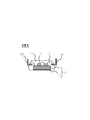

Classifications
-
- H—ELECTRICITY
- H10—SEMICONDUCTOR DEVICES; ELECTRIC SOLID-STATE DEVICES NOT OTHERWISE PROVIDED FOR
- H10W—GENERIC PACKAGES, INTERCONNECTIONS, CONNECTORS OR OTHER CONSTRUCTIONAL DETAILS OF DEVICES COVERED BY CLASS H10
- H10W70/00—Package substrates; Interposers; Redistribution layers [RDL]
- H10W70/40—Leadframes
- H10W70/461—Leadframes specially adapted for cooling
-
- H—ELECTRICITY
- H10—SEMICONDUCTOR DEVICES; ELECTRIC SOLID-STATE DEVICES NOT OTHERWISE PROVIDED FOR
- H10W—GENERIC PACKAGES, INTERCONNECTIONS, CONNECTORS OR OTHER CONSTRUCTIONAL DETAILS OF DEVICES COVERED BY CLASS H10
- H10W40/00—Arrangements for thermal protection or thermal control
- H10W40/10—Arrangements for heating
-
- H—ELECTRICITY
- H10—SEMICONDUCTOR DEVICES; ELECTRIC SOLID-STATE DEVICES NOT OTHERWISE PROVIDED FOR
- H10W—GENERIC PACKAGES, INTERCONNECTIONS, CONNECTORS OR OTHER CONSTRUCTIONAL DETAILS OF DEVICES COVERED BY CLASS H10
- H10W40/00—Arrangements for thermal protection or thermal control
- H10W40/20—Arrangements for cooling
- H10W40/25—Arrangements for cooling characterised by their materials
- H10W40/259—Ceramics or glasses
-
- H—ELECTRICITY
- H10—SEMICONDUCTOR DEVICES; ELECTRIC SOLID-STATE DEVICES NOT OTHERWISE PROVIDED FOR
- H10W—GENERIC PACKAGES, INTERCONNECTIONS, CONNECTORS OR OTHER CONSTRUCTIONAL DETAILS OF DEVICES COVERED BY CLASS H10
- H10W40/00—Arrangements for thermal protection or thermal control
- H10W40/70—Fillings or auxiliary members in containers or in encapsulations for thermal protection or control
- H10W40/77—Auxiliary members characterised by their shape
- H10W40/778—Auxiliary members characterised by their shape in encapsulations
-
- H—ELECTRICITY
- H10—SEMICONDUCTOR DEVICES; ELECTRIC SOLID-STATE DEVICES NOT OTHERWISE PROVIDED FOR
- H10W—GENERIC PACKAGES, INTERCONNECTIONS, CONNECTORS OR OTHER CONSTRUCTIONAL DETAILS OF DEVICES COVERED BY CLASS H10
- H10W70/00—Package substrates; Interposers; Redistribution layers [RDL]
- H10W70/40—Leadframes
- H10W70/421—Shapes or dispositions
- H10W70/424—Cross-sectional shapes
- H10W70/427—Bent parts
- H10W70/429—Bent parts being the outer leads
-
- H—ELECTRICITY
- H10—SEMICONDUCTOR DEVICES; ELECTRIC SOLID-STATE DEVICES NOT OTHERWISE PROVIDED FOR
- H10W—GENERIC PACKAGES, INTERCONNECTIONS, CONNECTORS OR OTHER CONSTRUCTIONAL DETAILS OF DEVICES COVERED BY CLASS H10
- H10W70/00—Package substrates; Interposers; Redistribution layers [RDL]
- H10W70/40—Leadframes
- H10W70/464—Additional interconnections in combination with leadframes
- H10W70/465—Bumps or wires
-
- H—ELECTRICITY
- H10—SEMICONDUCTOR DEVICES; ELECTRIC SOLID-STATE DEVICES NOT OTHERWISE PROVIDED FOR
- H10W—GENERIC PACKAGES, INTERCONNECTIONS, CONNECTORS OR OTHER CONSTRUCTIONAL DETAILS OF DEVICES COVERED BY CLASS H10
- H10W70/00—Package substrates; Interposers; Redistribution layers [RDL]
- H10W70/40—Leadframes
- H10W70/481—Leadframes for devices being provided for in groups H10D8/00 - H10D48/00
-
- H—ELECTRICITY
- H10—SEMICONDUCTOR DEVICES; ELECTRIC SOLID-STATE DEVICES NOT OTHERWISE PROVIDED FOR
- H10W—GENERIC PACKAGES, INTERCONNECTIONS, CONNECTORS OR OTHER CONSTRUCTIONAL DETAILS OF DEVICES COVERED BY CLASS H10
- H10W90/00—Package configurations
- H10W90/811—Multiple chips on leadframes
-
- H—ELECTRICITY
- H10—SEMICONDUCTOR DEVICES; ELECTRIC SOLID-STATE DEVICES NOT OTHERWISE PROVIDED FOR
- H10W—GENERIC PACKAGES, INTERCONNECTIONS, CONNECTORS OR OTHER CONSTRUCTIONAL DETAILS OF DEVICES COVERED BY CLASS H10
- H10W40/00—Arrangements for thermal protection or thermal control
- H10W40/20—Arrangements for cooling
- H10W40/25—Arrangements for cooling characterised by their materials
- H10W40/255—Arrangements for cooling characterised by their materials having a laminate or multilayered structure, e.g. direct bond copper [DBC] ceramic substrates
-
- H—ELECTRICITY
- H10—SEMICONDUCTOR DEVICES; ELECTRIC SOLID-STATE DEVICES NOT OTHERWISE PROVIDED FOR
- H10W—GENERIC PACKAGES, INTERCONNECTIONS, CONNECTORS OR OTHER CONSTRUCTIONAL DETAILS OF DEVICES COVERED BY CLASS H10
- H10W72/00—Interconnections or connectors in packages
- H10W72/071—Connecting or disconnecting
- H10W72/073—Connecting or disconnecting of die-attach connectors
-
- H—ELECTRICITY
- H10—SEMICONDUCTOR DEVICES; ELECTRIC SOLID-STATE DEVICES NOT OTHERWISE PROVIDED FOR
- H10W—GENERIC PACKAGES, INTERCONNECTIONS, CONNECTORS OR OTHER CONSTRUCTIONAL DETAILS OF DEVICES COVERED BY CLASS H10
- H10W72/00—Interconnections or connectors in packages
- H10W72/071—Connecting or disconnecting
- H10W72/073—Connecting or disconnecting of die-attach connectors
- H10W72/07331—Connecting techniques
- H10W72/07336—Soldering or alloying
-
- H—ELECTRICITY
- H10—SEMICONDUCTOR DEVICES; ELECTRIC SOLID-STATE DEVICES NOT OTHERWISE PROVIDED FOR
- H10W—GENERIC PACKAGES, INTERCONNECTIONS, CONNECTORS OR OTHER CONSTRUCTIONAL DETAILS OF DEVICES COVERED BY CLASS H10
- H10W72/00—Interconnections or connectors in packages
- H10W72/071—Connecting or disconnecting
- H10W72/073—Connecting or disconnecting of die-attach connectors
- H10W72/07341—Controlling the bonding environment, e.g. atmosphere composition or temperature
-
- H—ELECTRICITY
- H10—SEMICONDUCTOR DEVICES; ELECTRIC SOLID-STATE DEVICES NOT OTHERWISE PROVIDED FOR
- H10W—GENERIC PACKAGES, INTERCONNECTIONS, CONNECTORS OR OTHER CONSTRUCTIONAL DETAILS OF DEVICES COVERED BY CLASS H10
- H10W72/00—Interconnections or connectors in packages
- H10W72/071—Connecting or disconnecting
- H10W72/075—Connecting or disconnecting of bond wires
-
- H—ELECTRICITY
- H10—SEMICONDUCTOR DEVICES; ELECTRIC SOLID-STATE DEVICES NOT OTHERWISE PROVIDED FOR
- H10W—GENERIC PACKAGES, INTERCONNECTIONS, CONNECTORS OR OTHER CONSTRUCTIONAL DETAILS OF DEVICES COVERED BY CLASS H10
- H10W72/00—Interconnections or connectors in packages
- H10W72/071—Connecting or disconnecting
- H10W72/075—Connecting or disconnecting of bond wires
- H10W72/07531—Techniques
- H10W72/07532—Compression bonding, e.g. thermocompression bonding
- H10W72/07533—Ultrasonic bonding, e.g. thermosonic bonding
-
- H—ELECTRICITY
- H10—SEMICONDUCTOR DEVICES; ELECTRIC SOLID-STATE DEVICES NOT OTHERWISE PROVIDED FOR
- H10W—GENERIC PACKAGES, INTERCONNECTIONS, CONNECTORS OR OTHER CONSTRUCTIONAL DETAILS OF DEVICES COVERED BY CLASS H10
- H10W72/00—Interconnections or connectors in packages
- H10W72/071—Connecting or disconnecting
- H10W72/076—Connecting or disconnecting of strap connectors
-
- H—ELECTRICITY
- H10—SEMICONDUCTOR DEVICES; ELECTRIC SOLID-STATE DEVICES NOT OTHERWISE PROVIDED FOR
- H10W—GENERIC PACKAGES, INTERCONNECTIONS, CONNECTORS OR OTHER CONSTRUCTIONAL DETAILS OF DEVICES COVERED BY CLASS H10
- H10W72/00—Interconnections or connectors in packages
- H10W72/30—Die-attach connectors
- H10W72/351—Materials of die-attach connectors
- H10W72/352—Materials of die-attach connectors comprising metals or metalloids, e.g. solders
-
- H—ELECTRICITY
- H10—SEMICONDUCTOR DEVICES; ELECTRIC SOLID-STATE DEVICES NOT OTHERWISE PROVIDED FOR
- H10W—GENERIC PACKAGES, INTERCONNECTIONS, CONNECTORS OR OTHER CONSTRUCTIONAL DETAILS OF DEVICES COVERED BY CLASS H10
- H10W72/00—Interconnections or connectors in packages
- H10W72/50—Bond wires
- H10W72/531—Shapes of wire connectors
- H10W72/5363—Shapes of wire connectors the connected ends being wedge-shaped
-
- H—ELECTRICITY
- H10—SEMICONDUCTOR DEVICES; ELECTRIC SOLID-STATE DEVICES NOT OTHERWISE PROVIDED FOR
- H10W—GENERIC PACKAGES, INTERCONNECTIONS, CONNECTORS OR OTHER CONSTRUCTIONAL DETAILS OF DEVICES COVERED BY CLASS H10
- H10W72/00—Interconnections or connectors in packages
- H10W72/50—Bond wires
- H10W72/551—Materials of bond wires
- H10W72/552—Materials of bond wires comprising metals or metalloids, e.g. silver
- H10W72/5524—Materials of bond wires comprising metals or metalloids, e.g. silver comprising aluminium [Al]
-
- H—ELECTRICITY
- H10—SEMICONDUCTOR DEVICES; ELECTRIC SOLID-STATE DEVICES NOT OTHERWISE PROVIDED FOR
- H10W—GENERIC PACKAGES, INTERCONNECTIONS, CONNECTORS OR OTHER CONSTRUCTIONAL DETAILS OF DEVICES COVERED BY CLASS H10
- H10W72/00—Interconnections or connectors in packages
- H10W72/50—Bond wires
- H10W72/551—Materials of bond wires
- H10W72/552—Materials of bond wires comprising metals or metalloids, e.g. silver
- H10W72/5525—Materials of bond wires comprising metals or metalloids, e.g. silver comprising copper [Cu]
-
- H—ELECTRICITY
- H10—SEMICONDUCTOR DEVICES; ELECTRIC SOLID-STATE DEVICES NOT OTHERWISE PROVIDED FOR
- H10W—GENERIC PACKAGES, INTERCONNECTIONS, CONNECTORS OR OTHER CONSTRUCTIONAL DETAILS OF DEVICES COVERED BY CLASS H10
- H10W72/00—Interconnections or connectors in packages
- H10W72/50—Bond wires
- H10W72/59—Bond pads specially adapted therefor
-
- H—ELECTRICITY
- H10—SEMICONDUCTOR DEVICES; ELECTRIC SOLID-STATE DEVICES NOT OTHERWISE PROVIDED FOR
- H10W—GENERIC PACKAGES, INTERCONNECTIONS, CONNECTORS OR OTHER CONSTRUCTIONAL DETAILS OF DEVICES COVERED BY CLASS H10
- H10W72/00—Interconnections or connectors in packages
- H10W72/851—Dispositions of multiple connectors or interconnections
- H10W72/874—On different surfaces
- H10W72/884—Die-attach connectors and bond wires
-
- H—ELECTRICITY
- H10—SEMICONDUCTOR DEVICES; ELECTRIC SOLID-STATE DEVICES NOT OTHERWISE PROVIDED FOR
- H10W—GENERIC PACKAGES, INTERCONNECTIONS, CONNECTORS OR OTHER CONSTRUCTIONAL DETAILS OF DEVICES COVERED BY CLASS H10
- H10W72/00—Interconnections or connectors in packages
- H10W72/851—Dispositions of multiple connectors or interconnections
- H10W72/874—On different surfaces
- H10W72/886—Die-attach connectors and strap connectors
-
- H—ELECTRICITY
- H10—SEMICONDUCTOR DEVICES; ELECTRIC SOLID-STATE DEVICES NOT OTHERWISE PROVIDED FOR
- H10W—GENERIC PACKAGES, INTERCONNECTIONS, CONNECTORS OR OTHER CONSTRUCTIONAL DETAILS OF DEVICES COVERED BY CLASS H10
- H10W72/00—Interconnections or connectors in packages
- H10W72/90—Bond pads, in general
- H10W72/951—Materials of bond pads
- H10W72/952—Materials of bond pads comprising metals or metalloids, e.g. PbSn, Ag or Cu
-
- H—ELECTRICITY
- H10—SEMICONDUCTOR DEVICES; ELECTRIC SOLID-STATE DEVICES NOT OTHERWISE PROVIDED FOR
- H10W—GENERIC PACKAGES, INTERCONNECTIONS, CONNECTORS OR OTHER CONSTRUCTIONAL DETAILS OF DEVICES COVERED BY CLASS H10
- H10W74/00—Encapsulations, e.g. protective coatings
-
- H—ELECTRICITY
- H10—SEMICONDUCTOR DEVICES; ELECTRIC SOLID-STATE DEVICES NOT OTHERWISE PROVIDED FOR
- H10W—GENERIC PACKAGES, INTERCONNECTIONS, CONNECTORS OR OTHER CONSTRUCTIONAL DETAILS OF DEVICES COVERED BY CLASS H10
- H10W74/00—Encapsulations, e.g. protective coatings
- H10W74/10—Encapsulations, e.g. protective coatings characterised by their shape or disposition
- H10W74/111—Encapsulations, e.g. protective coatings characterised by their shape or disposition the semiconductor body being completely enclosed
-
- H—ELECTRICITY
- H10—SEMICONDUCTOR DEVICES; ELECTRIC SOLID-STATE DEVICES NOT OTHERWISE PROVIDED FOR
- H10W—GENERIC PACKAGES, INTERCONNECTIONS, CONNECTORS OR OTHER CONSTRUCTIONAL DETAILS OF DEVICES COVERED BY CLASS H10
- H10W74/00—Encapsulations, e.g. protective coatings
- H10W74/40—Encapsulations, e.g. protective coatings characterised by their materials
- H10W74/47—Encapsulations, e.g. protective coatings characterised by their materials comprising organic materials, e.g. plastics or resins
- H10W74/473—Encapsulations, e.g. protective coatings characterised by their materials comprising organic materials, e.g. plastics or resins containing a filler
-
- H—ELECTRICITY
- H10—SEMICONDUCTOR DEVICES; ELECTRIC SOLID-STATE DEVICES NOT OTHERWISE PROVIDED FOR
- H10W—GENERIC PACKAGES, INTERCONNECTIONS, CONNECTORS OR OTHER CONSTRUCTIONAL DETAILS OF DEVICES COVERED BY CLASS H10
- H10W90/00—Package configurations
- H10W90/701—Package configurations characterised by the relative positions of pads or connectors relative to package parts
- H10W90/731—Package configurations characterised by the relative positions of pads or connectors relative to package parts of die-attach connectors
- H10W90/736—Package configurations characterised by the relative positions of pads or connectors relative to package parts of die-attach connectors between a chip and a stacked lead frame, conducting package substrate or heat sink
-
- H—ELECTRICITY
- H10—SEMICONDUCTOR DEVICES; ELECTRIC SOLID-STATE DEVICES NOT OTHERWISE PROVIDED FOR
- H10W—GENERIC PACKAGES, INTERCONNECTIONS, CONNECTORS OR OTHER CONSTRUCTIONAL DETAILS OF DEVICES COVERED BY CLASS H10
- H10W90/00—Package configurations
- H10W90/701—Package configurations characterised by the relative positions of pads or connectors relative to package parts
- H10W90/751—Package configurations characterised by the relative positions of pads or connectors relative to package parts of bond wires
- H10W90/753—Package configurations characterised by the relative positions of pads or connectors relative to package parts of bond wires between laterally-adjacent chips
-
- H—ELECTRICITY
- H10—SEMICONDUCTOR DEVICES; ELECTRIC SOLID-STATE DEVICES NOT OTHERWISE PROVIDED FOR
- H10W—GENERIC PACKAGES, INTERCONNECTIONS, CONNECTORS OR OTHER CONSTRUCTIONAL DETAILS OF DEVICES COVERED BY CLASS H10
- H10W90/00—Package configurations
- H10W90/701—Package configurations characterised by the relative positions of pads or connectors relative to package parts
- H10W90/751—Package configurations characterised by the relative positions of pads or connectors relative to package parts of bond wires
- H10W90/756—Package configurations characterised by the relative positions of pads or connectors relative to package parts of bond wires between a chip and a stacked lead frame, conducting package substrate or heat sink
-
- H—ELECTRICITY
- H10—SEMICONDUCTOR DEVICES; ELECTRIC SOLID-STATE DEVICES NOT OTHERWISE PROVIDED FOR
- H10W—GENERIC PACKAGES, INTERCONNECTIONS, CONNECTORS OR OTHER CONSTRUCTIONAL DETAILS OF DEVICES COVERED BY CLASS H10
- H10W90/00—Package configurations
- H10W90/701—Package configurations characterised by the relative positions of pads or connectors relative to package parts
- H10W90/761—Package configurations characterised by the relative positions of pads or connectors relative to package parts of strap connectors
- H10W90/766—Package configurations characterised by the relative positions of pads or connectors relative to package parts of strap connectors between a chip and a stacked lead frame, conducting package substrate or heat sink
Definitions
- the present invention relates to a semiconductor module equipped with a circuit element such as a power semiconductor element.
- Semiconductor modules used in power supply devices are applied in a wide range from consumer equipment such as home air conditioners and refrigerators to industrial equipment such as inverters and servo controllers.
- a power semiconductor element or the like is mounted on a wiring board such as a metal base substrate or a ceramic substrate.
- a wiring board such as a metal base substrate or a ceramic substrate.
- One or a plurality of circuit elements such as power semiconductor elements are mounted on the wiring board, a plastic case frame is adhered, and the semiconductor module is formed by sealing with a silicone gel or an epoxy resin.
- a full mold semiconductor module by a transfer molding method is used (for example, refer to Patent Document 1).
- the lead frame and the heat sink are fixedly connected and electrical insulation is ensured.
- FIG. 7 shows a first example of a conventional full mold semiconductor module.
- a power semiconductor element 7 and a driving IC 31 are mounted on the external connection lead frames 9B and 9C, respectively, and are connected to each other by bonding wires 11 and 12. These parts are set in a mold, and a molding resin 14 is poured into the full mold semiconductor module.
- FIG. 8 shows a second example of a conventional full mold semiconductor module.
- a heat sink 32 is provided.
- the power semiconductor element 7 and the driving IC 31 are connected to each other by bonding wires 11 and 12, and the bonding wire 11 from the power semiconductor element 7 side is bonded to the external connection lead frame 9D.
- FIG. 9 shows a third example of a conventional full mold semiconductor module.
- the insulating substrate 33 is used so as to have two functions of an insulating layer and a heat sink.
- the insulating substrate 33 is a metal base substrate having a structure in which a metal plate 34 and a copper foil 35 are laminated via an insulating layer 36 made of resin, or a DBC (Direct Bond Copper where the insulating layer 36 is made of ceramics. ) A substrate or the like is used.
- the power semiconductor element 7 and the driving IC 31 are connected to each other by bonding wires 11 and 12, and the power semiconductor element 7 is connected to the external connection lead frame 9E through the bonding wire 11 and the copper foil 35.
- FIG. 10 shows a fourth example of a conventional full mold semiconductor module.
- an insulating metal block 37 in which ceramic layer is sprayed on one side of the metal block 1 to form the insulating layer 2 is used instead of the insulating substrate 33 in FIG. Since the power semiconductor element 7 is joined directly to the metal block 1, a device having better cooling performance than the third example has been developed.
- a bonding wire 11 from the power semiconductor element 7 is bonded to the external connection lead frame 9F.
- JP-A-9-139461 (paragraph number 0038, FIG. 1)
- the bonding wire 11 is directly bonded to the power semiconductor element 7 and one end thereof is bonded to an external lead terminal such as the external connection lead frame 9B.
- the heat generated during the operation of the power semiconductor element 7 is transmitted through the bonding wire 11 and the external lead terminal, and heats the external printed circuit board connected to the external lead terminal. If the printed circuit board is heated, the temperature in the case of a power conversion device such as an inverter that houses the printed circuit board rises and exceeds the heat resistance temperature of the member being used. For such a temperature rise, measures can be taken to cool by air cooling or water cooling, but this leads to an increase in the size and cost of the power conversion device.
- the present invention has been made in view of such a problem, and the object of the present invention is to respond to a request for measures against temperature increase in the power conversion device as described above, through an external lead terminal.
- An object of the present invention is to provide a semiconductor module excellent in heat dissipation that can effectively suppress heat flowing out to the printed circuit board side.
- the present invention provides a metal block having a first surface and a second surface, and a heat insulating layer formed by laminating a ceramic material directly on at least the first surface of the metal block.
- a relay electrode insulating layer formed by laminating a ceramic material directly on a part of the second surface of the metal block; and a relay electrode formed by laminating a metal material on the upper surface of the relay electrode insulating layer;
- a circuit element joined to the second surface of the metal block and an external lead terminal, and bonding wires or lead frames from the circuit element are joined to the relay electrode, and the relay electrode and the external lead terminal Are connected to each other (invention of claim 1).
- the bonding wire or the lead frame from the circuit element is joined to the relay electrode, and the relay electrode and the external lead terminal are connected, so that the circuit element and the external lead terminal can connect the relay electrode to the relay electrode. Connected through.
- circuit elements such as power semiconductor elements are generated during operation, and heat transferred along bonding wires or lead frames from the circuit elements mainly passes through the relay electrode and the insulating layer for the relay electrode made of a ceramic material. Therefore, the amount of heat transmitted to the external lead terminal can be sufficiently suppressed because it is transmitted to the metal block having a high heat capacity and excellent heat dissipation.
- the semiconductor module according to the present invention the amount of heat flowing from the external lead terminal to an external printed circuit board connected to the external lead terminal can be effectively suppressed. Can be effectively suppressed.
- the said insulating layer for thermal radiation can be set as the structure which covers at least one part of the side surface connected with the 1st surface of the said metal block (invention of Claim 2).
- the heat radiation insulating layer and the relay electrode insulating layer may have a thermal conductivity of 1 to 200 W / m ⁇ K and a thickness of 10 to 500 ⁇ m. invention).
- the heat dissipation insulating layer and the relay electrode insulating layer can be made of at least one filler group consisting of silicon oxide, aluminum oxide, silicon nitride, aluminum nitride, and boron nitride.
- the heat-dissipating insulating layer and the relay electrode insulating layer deposit ceramic fine particles of at least one of the filler groups by a plasma spraying method (invention of claim 5), or the heat dissipation.
- the insulating layer for a relay and the insulating layer for a relay electrode may be formed by depositing ceramic fine particles of at least one kind of the filler group by an aerosol deposition method (invention of claim 6).
- the relay electrode may be formed by spraying copper particles as a metal material (invention of claim 7). Further, the relay electrode and the external lead terminal can be connected via a bonding wire or a lead frame (invention of claim 8).
- the circuit element may be a power semiconductor element (invention of claim 9).
- heat generated by a circuit element such as a power semiconductor element in a semiconductor module during operation and transferred along a bonding wire or a lead frame from the circuit element is mainly relayed by a relay electrode and a ceramic material. Since the heat is transferred to the metal block having a high heat capacity and excellent heat dissipation through the electrode insulating layer, the amount of heat transferred to the external lead terminal can be sufficiently suppressed. Therefore, according to the present invention, it is possible to effectively suppress the amount of heat that flows from an external lead terminal to an external printed circuit board or the like connected to the external lead terminal, thereby preventing heating of the external printed circuit board or the like. It can be effectively suppressed. For this reason, the semiconductor module according to the present invention is suitable for effectively suppressing the temperature rise in the case of the power conversion device without increasing the size or cost of the power conversion device.
- FIG. 1 is a cross-sectional view showing a configuration example of a semiconductor module according to an embodiment of the present invention.
- FIGS. 1A to 1C show three configuration examples.
- a metal block 1 having a lower surface or first surface 1a in the drawing and an upper surface or second surface 1b in the drawing, and a first surface 1a of the metal block 1 and a side surface 1c connected thereto.
- the insulating layer for heat dissipation 2 formed so as to cover a part, the insulating layer for relay electrode 4 formed on a part of the second surface 1b of the metal block 1, and the upper surface of the insulating layer 4 for relay electrode
- the relay electrode 3, the power semiconductor element 7 joined to the second surface 1 b of the metal block 1 by the solder 23, and the lead frame 9 for external connection are provided, and the bonding wire 11 a from the power semiconductor element 7 is attached to the relay electrode 3.
- the relay electrode 3 and the external connection lead frame 9 are connected by the bonding wire 11b, and the semiconductor module 51 is comprised.
- the external connection lead frame 9 functions as an external lead terminal of the semiconductor module 51.
- a bonding wire for connecting the power semiconductor element 7 and the relay electrode 3 is denoted by 11a
- a bonding wire for connecting the relay electrode 3 and the external connection lead frame 9 is denoted by 11b.
- the metal block 1 is made of copper, which is a metal material having good conductivity and heat conductivity, and its thickness is set to about 1.0 to 4.0 mm so that the heat capacity is high and the heat dissipation is excellent. It is said.
- the heat-dissipating insulating layer 2 formed on the first surface 1a side of the metal block 1 is formed of a ceramic material having excellent thermal conductivity, such as aluminum oxide, silicon nitride, aluminum nitride, or boron nitride. I am doing so.
- the heat dissipation insulating layer 2 preferably has a thermal conductivity of 1 to 200 W / m ⁇ K, and a thickness of 10 to 500 ⁇ m.
- the ceramics excellent in thermal conductivity are provided on the first surface 1a side of the metal block 1 in which the power semiconductor element 7 is mounted on the second surface 1b side and has high heat capacity and excellent heat dissipation. Since the heat dissipation insulating layer 2 made of a material is formed, the first surface 1a of the metal block 1 is in direct contact with an external cooling heat sink (not shown) through the heat dissipation insulating layer 2, thereby providing a power semiconductor. The thermal resistance at the lower part of the element 7 can be sufficiently reduced, and excellent heat dissipation can be achieved.
- the number of power semiconductor elements 7 mounted on the metal block 1 may be two, or 3 It may be more than one.
- the metal material forming the metal block 1 is not limited to copper, and for example, a copper alloy, aluminum, an aluminum alloy, or the like is also applicable.
- the insulating layer 4 for the relay electrode formed on the second surface 1b side of the metal block 1 is also formed of a ceramic material having excellent thermal conductivity such as aluminum oxide, silicon nitride, aluminum nitride, boron nitride. Like to do.
- the insulating layer 4 for relay electrodes preferably has a thermal conductivity of 1 to 200 W / m ⁇ K, and a thickness of 10 to 500 ⁇ m.
- the relay electrode 3 formed on the upper surface of the relay electrode insulating layer 4 is made of a metal material having excellent thermal conductivity, such as copper.
- the metal material which forms the relay electrode 3 is not restricted to copper, For example, copper alloy, aluminum, aluminum alloy etc. are applicable.
- FIG. 2 is a diagram schematically showing the heat flow in the semiconductor module according to the embodiment of the present invention. In particular, the case where the semiconductor module 51 is incorporated in the power conversion device 101 will be described.
- the semiconductor module 51 is mounted on the cooling heat sink 102 so that the heat-dissipating insulating layer 2 is in contact, and the external connection lead frame 9 is disposed on the semiconductor module 51. Is connected to the power conversion device 101.
- a main circuit is configured by the power semiconductor element 7 in the semiconductor module 51, and other electronic circuit components 115 a, 115 b, 115 c and the like mounted on the printed wiring board 114 in the printed wiring board portion 111, and the like.
- a power supply circuit and a control circuit are configured.
- the electronic circuit components 115a, 115b, and 115c various components such as an IC, an LSI, a resistor, a capacitor, and a reactor are used.
- FIG. 2 only a part of the printed wiring board 114 is illustrated in which a circuit pattern 113 is formed on the printed circuit board body 112, and electronic circuit components 115 a, 115 b, 115 c, etc. are formed on the printed wiring board 114 by solder 116.
- the printed wiring board portion 111 is configured by bonding.
- the external connection lead frame 9 of the semiconductor module 51 is inserted into the insertion hole 118 of the printed wiring board 114 and connected to the circuit pattern 113 by soldering 117.
- connection structure between the semiconductor module and the printed wiring board portion according to the embodiment of the present invention is not limited to the configuration shown in FIG. In FIG. 2, for example, an IGBT (Insulated Gate) is used as the power semiconductor element 7 in the semiconductor module 51.
- IGBT Insulated Gate
- the collector electrode on the lower surface of the IGBT is joined to the second surface 1b of the metal block 1, and the emitter electrode and the gate electrode formed on the upper surface of the IGBT are respectively connected to the relay electrode by the bonding wire 11a. 3 is connected.
- FIG. 2 the flow of heat when the power semiconductor element 7 in the semiconductor module 51 generates heat during operation is schematically shown by white arrows h1 to h5.
- the widths of the white arrows h1 to h5 qualitatively indicate the magnitude of the flowing heat.
- FIG. 2 shows only the heat flow from the power semiconductor element 7 along the left bonding wire 11a.
- a bonding wire for connecting the power semiconductor element 7 and the relay electrode 3 is denoted by 11a
- a bonding wire for connecting the relay electrode 3 and the external connection lead frame 9 is denoted by 11b.
- heat generated during operation of the power semiconductor element 7 in the semiconductor module 51 is transmitted from the power semiconductor element 7 to the cooling heat sink 102 via the solder layer 23, the metal block 1, and the heat dissipation insulating layer 2. At the same time, it is also transmitted from the power semiconductor element 7 to the external connection lead frame 9 side through the bonding wire 11a.
- the relay electrode 3 formed on the metal block 1 via the relay electrode insulating layer 4 is provided, and the bonding wire 11a from the power semiconductor element 7 is joined to the relay electrode 3.
- the relay electrode 3 is connected to the external connection lead frame 9 via another bonding wire 11b.
- the semiconductor module 51 most of the heat flowing from the power semiconductor element 7 via the bonding wire 11a is the relay electrode 3, the relay electrode insulating layer 4 made of a ceramic material having excellent thermal conductivity, and the metal.
- the amount of heat transmitted to the cooling heat sink 102 via the block 1 and transmitted to the external connection lead frame 9 side from the relay electrode 3 via the bonding wire 11b is suppressed to be sufficiently small.
- the amount of heat transmitted to the printed wiring board 111 side connected to the external connection lead frame 9 of the semiconductor module 51 can be suppressed, and heating to the printed wiring board 114 forming the printed wiring board 111 is effective. Can be suppressed.
- the semiconductor module 51 as described above, as shown in FIG.
- the heat generated by the power semiconductor element 7 during operation is the first heat transfer of the power semiconductor element 7 ⁇ the solder layer 23 ⁇ the metal block 1. Since it can be efficiently transmitted to the metal block 1 through the two heat transfer paths of the path and the power semiconductor element 7 ⁇ bonding wire 11a ⁇ relay electrode 3 ⁇ relay electrode insulating layer 4 ⁇ second heat transfer path of the metal block 1, The function of the metal block 1 having a high heat capacity and excellent heat dissipation is utilized more effectively.
- FIG. 11 is a diagram schematically showing a heat flow in a semiconductor module according to the prior art as a comparative example.
- the semiconductor module having the configuration described in FIG.
- the case where 151 is incorporated in the power conversion device 201 will be described.
- the semiconductor module 151 is mounted on the cooling heat sink 202 so that the heat-dissipating insulating layer 2 is in contact with it, and the printed wiring board portion in which the lead frame 9 for external connection is disposed above the semiconductor module 151.
- the power conversion device 201 is configured by being connected to 111A.
- the configuration of the printed wiring board portion 111A is the same as that shown in FIG. 2 except that the arrangement of the circuit pattern and the electronic circuit component corresponds to the arrangement of the external connection lead frame 9 in the semiconductor module 151.
- the connection structure between the semiconductor module 151 and the printed wiring board portion 111A in FIG. 11 is the same as the connection structure between the semiconductor module 51 and the printed wiring board portion 111 in FIG.
- FIG. 11 the flow of heat when the power semiconductor element 7 in the semiconductor module 151 generates heat during operation is schematically shown by white arrows h11 to h13.
- the widths of the white arrows h11 to h13 qualitatively indicate the amount of heat flowing.
- FIG. 11 only the heat flow from the power semiconductor element 7 along the left bonding wire 11 is shown.
- heat generated during operation of the power semiconductor element 7 in the semiconductor module 151 is transferred from the power semiconductor element 7 to the cooling heat sink 202 via the solder layer 23, the metal block 1, and the heat dissipation insulating layer 2. At the same time, it is also transmitted from the power semiconductor element 7 to the lead frame 9 side for external connection through the bonding wire 11.
- the bonding wire 11 from the power semiconductor element 7 is directly connected to the lead frame 9 for external connection. Therefore, the heat flowing from the power semiconductor element 7 via the bonding wire 11 Flows through the external connection lead frame 9 as it is. Thereby, in the semiconductor module 151, since the amount of heat transmitted to the printed wiring board portion 111A connected to the lead frame 9 for external connection of the semiconductor module 151 cannot be suppressed, the printed wiring board forming the printed wiring board portion 111A. Heating to 114A cannot be suppressed.
- the semiconductor module according to the present invention in the state where the power semiconductor element in the semiconductor module is operated in the state of being incorporated in an electric device such as a power conversion device, the amount of heat transmitted to the connected printed wiring board portion side can be suppressed, and heating to the printed wiring board and the like can be effectively suppressed.
- FIG. 1B A semiconductor module 51A shown in FIG. 1B is connected to the semiconductor module 51 shown in FIG. 1A instead of connecting the relay electrode 3 and the external connection lead frame 9 with bonding wires 11b.
- the difference is that the connecting lead frame 9A is directly joined to the relay electrode 3, and the other points are the same.
- a semiconductor module 51B shown in FIG. 1C is a lead frame instead of connecting the power semiconductor element 7 and the relay electrode 3 to the semiconductor module 51A shown in FIG. 13 is different, and the other points are the same.
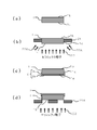
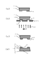
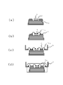
- FIGS. 3 to 5 are cross-sectional views showing the structure of each stage in the manufacturing process of the semiconductor module according to the embodiment of the present invention.
- the semiconductor module 51 shown in FIG. is there.
- a metal block 1 is manufactured by punching a copper plate having a thickness of about 1.0 to 4.0 mm into a square or a rectangle by pressing (FIG. 3A).
- the insulating layer 2 for heat dissipation is formed on the first surface 1a side of the metal block 1 by applying a mask 21 and laminating ceramic powders 22 such as aluminum oxide powder by a thermal spraying method or an aerosol deposition method. .
- the first surface insulating layer 2a is formed on the first surface 1a of the metal block 1
- the side surface insulating layer 2b is formed on a part of the side surface 1c of the metal block 1.
- the side surface insulating layer 2b is formed so as to be connected to the first surface insulating layer 2a (FIGS. 3B to 3C).
- the ceramic powder is made of silicon oxide, aluminum oxide, silicon nitride, aluminum nitride, boron nitride. Use the above.
- thermal spraying is performed on the metal block 1 through the mask 21 under atmospheric pressure or reduced pressure, and the insulating layer 2 for heat dissipation is deposited.
- the side surface insulating layer 2b is formed on the metal block 1 as the heat insulating layer 2 in addition to the first surface insulating layer 2a by the plasma spraying method, for example, as shown in FIG.
- the ceramic powder is sprayed as the raw material powders 22 and 22A.
- the metal block 1 is used.
- a side surface insulating layer 2b connected to the first surface insulating layer 2a is also formed on a part of the side surface 1c.
- the range of the side surface 1c of the metal block 1 covered by the side surface insulating layer 2b is determined in consideration of insulation design conditions such as a potential difference that may occur between the metal block 1 and an external cooling heat sink (not shown).
- the thickness of the heat radiation insulating layer 2 can be adjusted by controlling the spraying time.
- the thickness of the insulating layer is preferably 10 to 500 ⁇ m.
- the insulating layer 2 for heat dissipation formed as described above has, for example, a thickness of 200 ⁇ m and an AC breakdown voltage of 5 kV or more as an insulating property, and can also be used for a power element having a withstand voltage rating of 1200 V.
- the aerosol deposition method is a technique in which fine particles or ultrafine particles are mixed with gas to form an aerosol, and a film is formed on a substrate through a nozzle. Helium or air is used as the gas.
- the apparatus can be composed of an aerosolization chamber and a film formation chamber (not shown). The film forming chamber is depressurized to about 50 Pa to 1 kPa by a vacuum pump.
- the raw fine or ultrafine particle material is dried to be aerosolized by stirring and mixing with gas in the aerosol chamber and transported to the film formation chamber by the gas flow generated by the pressure difference between the two chambers. , And is sprayed to the first surface 1a side of the metal block 1 that is the film formation target.
- the raw material fine particles ceramic powder mechanically pulverized to a particle size of 0.1 to 2 ⁇ m is used.
- the ultrafine particles transported by the gas are accelerated up to several hundreds m / sec by passing through a nozzle having a minute opening in a decompressed chamber.
- the film formation speed and the density of the film are largely dependent on the particle size, aggregated state, and dry state of the ceramic fine particles used, so the aggregated particle crusher and classification between the aerosolization chamber and the film formation chamber
- the device is used.
- the heat-dissipating insulating layer 2 As a film, fine ceramic particles having a particle diameter of 0.1 to 2 ⁇ m are sprayed onto the substrate at a high speed, and the impact energy at that time is applied to microcrystalline particles of about 10 to 30 nm. By crushing, forming a new surface, activating the surface, and bonding the particles together, a ceramic film having a dense nanocrystalline structure is formed. Further, in the aerosol deposition method, a ceramic film can be formed at room temperature without particularly applying a temperature.
- any one of aluminum oxide, silicon nitride, aluminum nitride, and boron nitride having a particle size of about 0.1 to 2 ⁇ m for the aerosol deposition fine particles.
- fine particles are sprayed using a mask 21 for a predetermined time to form a heat radiation insulating layer 2 shown in FIG.
- the side surface insulating layer 2b is formed on the metal block 1 as the insulating layer 2 in addition to the first surface insulating layer 2a by the aerosol deposition method, as in the case of the plasma spraying method described above, for example, FIG. As shown in b), ceramic fine particles are sprayed as the raw material powders 22 and 22A in a state where a part of the side surface 1c of the metal block 1 is exposed from the mask 21.
- the side surface insulating layer 2b connected to the first surface insulating layer 2a is also formed on a part of the side surface 1c.
- the range of the side surface 1c of the metal block 1 covered by the side surface insulating layer 2b is determined in consideration of insulation design conditions such as a potential difference that may occur between the metal block 1 and an external cooling heat sink (not shown).
- the fine particles are formed by forming a film of aluminum oxide on a filler of silicon nitride, aluminum nitride, or boron nitride, or formed a film of silicon oxide on a filler of silicon nitride, aluminum nitride, or boron nitride. Things are also applicable. If these fine particles are used, an insulating layer composed of two or more kinds of ceramics can be formed.
- the thickness of the heat radiation insulating layer 2 is preferably 10 to 500 ⁇ m, which is the same as in the spraying method.
- the insulating layer 2 formed as described above has an insulation characteristic of, for example, a thickness of 200 ⁇ m, an AC breakdown voltage of 5 kV or more, and can be used for a power element having a withstand voltage rating of 1200 V.
- the second surface 1b of the metal block 1 is laminated by applying a mask 21A to the second surface 1b of the metal block 1 and laminating ceramic powder 22 such as aluminum oxide powder by a thermal spraying method or an aerosol deposition method.
- a relay electrode insulating layer 4 is formed on the side (FIGS. 3D to 4A).
- the insulating layer 2 for the relay electrode is formed not on the entire surface of the second surface 1b of the metal block 1 but on a part thereof.
- the material of the ceramic fine particles used for forming the insulating layer 4 for the relay electrode and the forming method of the insulating layer are the same as those of the insulating layer 2 for heat dissipation in both the thermal spraying method and the aerosol deposition method.
- the thickness of the insulating layer 2 for the relay electrode is preferably 10 to 500 ⁇ m, like the insulating layer 2 for heat dissipation, regardless of whether it is formed by the thermal spraying method or the aerosol deposition method.
- the copper relay electrode 3 is laminated on the relay electrode insulating layer 4.
- a plasma spraying method is used as in the case of the insulating layer. That is, the mask 21B is applied to the relay electrode insulating layer 4 formed on the second surface 1b of the metal block 1, and the copper particles 24 are sprayed to form the relay electrode 3 (FIGS. 4B to 4C). )).
- the insulating layer 2 for heat dissipation is formed on the first surface 1a side of the metal block 1, and the relay electrode 3 is formed on a part of the second surface 1b via the insulating layer 4 for relay electrode.
- the metal block 5 is completed (FIG. 4 (d)).
- the power semiconductor element 7 is joined to the second surface 1b of the metal block 1 in the insulating metal block 5 by joining with the solder 23 (FIG. 5A).
- Soldering is performed in a furnace capable of hydrogen reduction using pelletized solder. The reason why a furnace capable of hydrogen reduction is used is to improve the wettability with the solder by removing and activating the oxide film on the surface of the metal block 1 by hydrogen reduction.
- solder material for example, high-temperature solder made of SnPbAg or lead-free solder made of SnAgCu is used.
- the soldering temperature is set according to the melting point of the solder. If voids remain in the solder layer 23 between the power semiconductor element 7 and the metal block 1, the thermal resistance increases, and heat generated from the power semiconductor element 7 cannot be efficiently radiated. Therefore, vacuuming of 1.3 kPa (10 Torr) or less is performed in a state where the solder is melted so as not to generate voids. Next, the power semiconductor element 7 and the relay electrode 3 are connected by the bonding wire 11a (FIG. 5B).
- the bonding wire 11a is ultrasonically bonded using an Al wire having a wire diameter of 125 to 500 ⁇ m.
- a lead frame 13 may be used as shown in FIG. 1C instead of the bonding wire 11a.
- the relay electrode 3 and the external lead terminal 9 are connected by the bonding wire 11b (FIG. 5C).
- the bonding wire 11b is ultrasonically bonded using an Al wire having a wire diameter of 125 to 500 ⁇ m, similarly to the bonding wire 11a described above.
- a lead frame similar to the lead frame 13 shown in FIG. 1C may be used instead of the bonding wire 11b.
- the lead frame 9 for external connection may be directly joined to the relay electrode 3 as shown in FIGS.
- the assembly shown in FIG. 5C is set in a mold attached to a transfer molding machine.
- the mold is kept at a temperature of about 170 to 180 ° C.
- the tablet-like epoxy resin 14 is poured into the mold by a plunger.
- the epoxy resin 14 is made of an epoxy resin containing at least one filler group consisting of silicon oxide, aluminum oxide, silicon nitride, aluminum nitride, and boron nitride, and has a thermal conductivity of 0.5 to 5 W / m ⁇ K. Use.
- FIG. 6 is a cross-sectional view showing a different configuration example of the semiconductor module according to the embodiment of the present invention.
- the heat radiation insulating layer 2 may be formed only on the first surface.
- the configurations of the semiconductor modules 51C, 51D, and 51E respectively correspond to the configurations of the semiconductor modules 51, 51A, and 51B shown in FIGS. 1A to 1C except for the points described above.
- a bonding wire or a lead frame from a circuit element such as a power semiconductor element bonded to the second surface of the metal block is bonded to the relay electrode, and then the relay electrode and the external lead are connected.
- the circuit element is generated during operation, and the heat transferred along the bonding wire or lead frame from the circuit element is mainly from the relay electrode and ceramic material with excellent thermal conductivity.
- the semiconductor module according to the present invention Since the heat is transferred to the metal block having high heat capacity and excellent heat dissipation through the relay electrode insulating layer, the amount of heat transferred to the external lead terminal can be sufficiently suppressed. As a result, in the semiconductor module according to the present invention, the amount of heat flowing from the external lead terminal to an external printed circuit board connected to the external lead terminal can be effectively suppressed. Therefore, by using such a semiconductor module, it is possible to effectively suppress the temperature rise in the case of the power conversion device without increasing the size or cost of the power conversion device. .
- Metal block 1a First surface 1b: Second surface 1c: Side surface 2: Heat radiation insulating layer 2a: First surface portion insulating layer 2b: Side surface insulating layer 3: Relay electrode 4: Relay electrode insulating layer 5: Insulation Metal block 7: Power semiconductor element 9, 9A, 9B, 9C, 9D, 9E, 9F: External connection lead frame 11, 11a, 11b: Bonding wire 12: IC bonding wire 13: Lead frame 14: Molding resin (epoxy resin) 21, 21A, 21B: Masks 22, 22A: Ceramic particles 23: Solder 24: Copper particles 31: Driving IC 32: Heat sink 33: Insulating substrate 34: Metal plate 35: Copper foil 36: Insulating layer 37: Insulating metal blocks 51, 51A, 51B, 51C, 51D, 51E: Semiconductor module 101: Power conversion device 102: Heat sink 111 for cooling 111A: Printed wiring board portion 112, 112A: Printed circuit board body 113, 113A: Circuit pattern 114, 114A:
Landscapes
- Cooling Or The Like Of Semiconductors Or Solid State Devices (AREA)
- Chemical & Material Sciences (AREA)
- Engineering & Computer Science (AREA)
- Ceramic Engineering (AREA)
- Materials Engineering (AREA)
Abstract
金属ブロック1と、金属ブロック1の少なくとも第1面1a側に直接セラミックス材料を積層して形成された放熱用絶縁層2と、金属ブロック1の第2面1bの一部分に直接セラミックス材料を積層して形成された中継電極用絶縁層4と、中継電極用絶縁層4の上面に金属材料を積層して形成された中継電極3と、金属ブロック1の第2面1bにはんだ23により接合された回路素子7と、外部リード端子9とを備え、回路素子7からのボンディングワイヤ11aまたはリードフレーム13を中継電極3に接合するとともに、中継電極3と外部リード端子9とを接続した構成とする。
Description
本発明は、パワー半導体素子などの回路素子を搭載した半導体モジュールに関する。
電源装置に使用される半導体モジュールは、家庭用エアコン、冷蔵庫などの民生機器から、インバータ、サーボコントローラなどの産業機器まで、広範囲に渡って適用されている。半導体モジュールでは、消費電力の点から、パワー半導体素子などは金属ベース基板やセラミックス基板などの配線板に搭載される。この配線板にパワー半導体素子などの1つまたは複数の回路素子を搭載し、プラスチックケース枠を接着し、シリコーンゲルやエポキシ樹脂などで封止することによって半導体モジュールを構成する。
一方、製造コストを低減するために、トランスファー成形方式によるフルモールド半導体モジュールが用いられている(例えば、特許文献1参照)。フルモールド半導体モジュールでは、リードフレームとヒートシンクとを固定的に連結するとともに、電気的絶縁を確保している。
図7に従来のフルモールド半導体モジュールの第1例を示す。外部接続用リードフレーム9B、9Cの上にはそれぞれパワー半導体素子7、駆動IC31が実装され、ボンディングワイヤ11、12により相互に接続されている。これらの部品を金型にセットして、成形樹脂14を流し込むことにより、フルモールド半導体モジュールを構成する。
図8に従来のフルモールド半導体モジュールの第2例を示す。図7に示したフルモールド半導体モジュールに加えて、ヒートシンク32を設けたものである。パワー半導体素子7、駆動IC31がボンディングワイヤ11、12により相互に接続されているとともに、パワー半導体素子7側からのボンディングワイヤ11が外部接続用リードフレーム9Dに接合されている。
さらに、図9に従来のフルモールド半導体モジュールの第3例を示す。第3例では絶縁基板33を用いて絶縁層とヒートシンクとの2つの機能を兼ねるようにしている。絶縁基板33には、図示のように金属板34と銅箔35とを樹脂からなる絶縁層36を介して積層した構造の金属ベース基板、もしくは、絶縁層36がセラミックスからなるDBC(Direct Bond Copper)基板などが用いられる。パワー半導体素子7、駆動IC31がボンディングワイヤ11、12により相互に接続されているとともに、パワー半導体素子7がボンディングワイヤ11および銅箔35を介して外部接続用リードフレーム9Eに接続されている。
また、図10に従来のフルモールド半導体モジュールの第4例を示す。第4例は、図9における絶縁基板33の代わりに、金属ブロック1の片面にセラミックスを溶射し絶縁層2を形成した絶縁金属ブロック37を用いる構成である。金属ブロック1に直接パワー半導体素子7を接合するので、第3例より冷却性に優れたものが開発されている。パワー半導体素子7からのボンディングワイヤ11が外部接続用リードフレーム9Fに接合されている。
しかしながら,従来の第1~4例のフルモールド半導体モジュールの場合、パワー半導体素子7にボンディングワイヤ11を直接接合して、その一端を外部接続用リードフレーム9Bなどの外部リード端子に接合し、この外部リード端子から電流を取り出すため、パワー半導体素子7の動作時に発生する熱が、ボンディングワイヤ11および外部リード端子を伝わり、外部リード端子と接続される外部のプリント基板を加熱することになる。
プリンド基板を加熱してしまうと、プリント基板を収納している例えばインバータなど電力変換機器のケース内の温度が上昇してしまい、使用している部材の耐熱温度を超えてしまう。このような温度上昇に対しては、空冷もしくは水冷方式で冷却する対策も可能であるが、電力変換機器の寸法増大やコスト増大に繋がってしまう。このため、電力変換機器の寸法増大やコスト増大なしに上述のような電力変換機器のケース内の温度上昇を効果的に抑制可能な対策が必要となっており、そのような対策の一つとして、半導体モジュールから外部リード端子を介して外部のプリント基板側に流れ出す熱を効果的に抑制することが求められている。
プリンド基板を加熱してしまうと、プリント基板を収納している例えばインバータなど電力変換機器のケース内の温度が上昇してしまい、使用している部材の耐熱温度を超えてしまう。このような温度上昇に対しては、空冷もしくは水冷方式で冷却する対策も可能であるが、電力変換機器の寸法増大やコスト増大に繋がってしまう。このため、電力変換機器の寸法増大やコスト増大なしに上述のような電力変換機器のケース内の温度上昇を効果的に抑制可能な対策が必要となっており、そのような対策の一つとして、半導体モジュールから外部リード端子を介して外部のプリント基板側に流れ出す熱を効果的に抑制することが求められている。
本発明は、このような問題に鑑みてなされたものであり、その目的とするところは、上述のような電力変換機器内の温度上昇対策に関する要求に応えて、外部リード端子を介して外部のプリント基板側に流れ出す熱を効果的に抑制できる、放熱性に優れた半導体モジュールを提供することにある。
本発明は、このような目的を達成するために、第1面および第2面を有する金属ブロックと、前記金属ブロックの少なくとも第1面に直接セラミックス材料を積層して形成された放熱用絶縁層と、前記金属ブロックの第2面の一部分に直接セラミックス材料を積層して形成された中継電極用絶縁層と、前記中継電極用絶縁層の上面に金属材料を積層して形成された中継電極と、前記金属ブロックの第2面に接合された回路素子と、外部リード端子とを備え、前記回路素子からのボンディングワイヤまたはリードフレームを前記中継電極に接合するとともに、前記中継電極と前記外部リード端子とを接続した構成とする(請求項1の発明)。
この構成によれば、回路素子からのボンディングワイヤまたはリードフレームを中継電極に接合するとともに、中継電極と外部リード端子とを接続していることにより、回路素子と外部リード端子とは上記中継電極を介して接続されている。
このため、パワー半導体素子などの回路素子が動作時に発生し、回路素子からのボンディングワイヤまたはリードフレームに沿って伝達される熱は、主に中継電極およびセラミックス材料からなる中継電極用絶縁層を介して熱容量が高く放熱性に優れた金属ブロックの方に伝わるので、外部リード端子の方に伝わる熱量は十分に抑制することができる。
このため、本発明による半導体モジュールでは、その外部リード端子から当該外部リード端子に接続された外部の例えばプリント基板などに流れ出す熱量を効果的に抑制することができるので、外部のプリント基板などに対する加熱を効果的に抑制することができる。
この構成によれば、回路素子からのボンディングワイヤまたはリードフレームを中継電極に接合するとともに、中継電極と外部リード端子とを接続していることにより、回路素子と外部リード端子とは上記中継電極を介して接続されている。
このため、パワー半導体素子などの回路素子が動作時に発生し、回路素子からのボンディングワイヤまたはリードフレームに沿って伝達される熱は、主に中継電極およびセラミックス材料からなる中継電極用絶縁層を介して熱容量が高く放熱性に優れた金属ブロックの方に伝わるので、外部リード端子の方に伝わる熱量は十分に抑制することができる。
このため、本発明による半導体モジュールでは、その外部リード端子から当該外部リード端子に接続された外部の例えばプリント基板などに流れ出す熱量を効果的に抑制することができるので、外部のプリント基板などに対する加熱を効果的に抑制することができる。
そして、前記放熱用絶縁層は、前記金属ブロックの第1面に連接する側面の少なくとも一部を覆う構成とすることができる(請求項2の発明)。
また、前記放熱用絶縁層および前記中継電極用絶縁層は、熱伝導率が1~200W/m・Kであり、かつ厚さが10~500μmである構成とすることができる(請求項3の発明)。
また、前記放熱用絶縁層および前記中継電極用絶縁層は、熱伝導率が1~200W/m・Kであり、かつ厚さが10~500μmである構成とすることができる(請求項3の発明)。
また、前記放熱用絶縁層および前記中継電極用絶縁層は、酸化珪素、酸化アルミニウム、窒化珪素、窒化アルミニウム、窒化ホウ素からなるフィラー群の少なくとも1種類からなる構成とすることができ(請求項4の発明)、さらに、前記放熱用絶縁層および前記中継電極用絶縁層は、前記フィラー群の少なくとも1種によるセラミックス微粒子をプラズマ溶射法にて堆積させること(請求項5の発明)や、前記放熱用絶縁層および前記中継電極用絶縁層は、前記フィラー群の少なくとも1種によるセラミックス微粒子をエアロゾルデポジション法にて堆積させることにより形成した構成とすることもできる(請求項6の発明)。
また、前記中継電極は、金属材料として銅粒子を溶射して形成した構成とすることができる(請求項7の発明)。
また、前記中継電極と外部リード端子とをボンディングワイヤまたはリードフレームを介して接続した構成とすることができる(請求項8の発明)。
また、前記中継電極と外部リード端子とをボンディングワイヤまたはリードフレームを介して接続した構成とすることができる(請求項8の発明)。
そして、前記回路素子は、パワー半導体素子である構成とすることができる(請求項9の発明)。
本発明によれば、半導体モジュールにおけるパワー半導体素子などの回路素子が動作時に発生し、回路素子からのボンディングワイヤまたはリードフレームに沿って伝達される熱は、主に中継電極およびセラミックス材料からなる中継電極用絶縁層を介して熱容量が高く放熱性に優れた金属ブロックの方に伝わるので、外部リード端子の方に伝わる熱量は十分に抑制することができる。
したがって、本発明によれば、外部リード端子から当該外部リード端子に接続された外部の例えばプリント基板などに流れ出す熱量を効果的に抑制することができ、これにより、外部のプリント基板などに対する加熱を効果的に抑制することができる。
このため、本発明による半導体モジュールは、電力変換機器の寸法増大やコスト増大なしに電力変換機器のケース内の温度上昇を効果的に抑制する上で好適なものとなっている。
したがって、本発明によれば、外部リード端子から当該外部リード端子に接続された外部の例えばプリント基板などに流れ出す熱量を効果的に抑制することができ、これにより、外部のプリント基板などに対する加熱を効果的に抑制することができる。
このため、本発明による半導体モジュールは、電力変換機器の寸法増大やコスト増大なしに電力変換機器のケース内の温度上昇を効果的に抑制する上で好適なものとなっている。
以下、図面を参照しながら、本発明の実施形態について詳細に説明する。なお、本発明は、下記の実施形態に限定されるものではなく、その要旨を変更しない範囲内で適宜変形して実施することができるものである。また、以下の説明に際し、全図にわたり、特に言及がない限り、共通する部分または要素には、共通する参照符号が付されている。
図1は本発明の実施形態にかかる半導体モジュールの構成例を示す断面図であり、図1(a)~(c)に3通りの構成例を示している。
図1(a)の構成例では、図における下面すなわち第1面1aおよび図における上面すなわち第2面1bを有する金属ブロック1と、金属ブロック1の第1面1aおよびこれに連接する側面1cの一部を覆うように形成された放熱用絶縁層2と、金属ブロック1の第2面1bの一部分に形成された中継電極用絶縁層4と、中継電極用絶縁層4の上面に形成された中継電極3と、金属ブロック1の第2面1bにはんだ23により接合されたパワー半導体素子7と、外部接続用リードフレーム9とを備え、パワー半導体素子7からのボンディングワイヤ11aを中継電極3に接合するとともに、中継電極3と外部接続用リードフレーム9とをボンディングワイヤ11bで接続して、半導体モジュール51が構成されている。ここで、外部接続用リードフレーム9は半導体モジュール51の外部リード端子として機能するものである。また、図1では、説明の便宜上、パワー半導体素子7と中継電極3とを接続するボンディングワイヤを11aとし、中継電極3と外部接続用リードフレーム9とを接続するボンディングワイヤを11bとしている。
図1(a)の構成例では、図における下面すなわち第1面1aおよび図における上面すなわち第2面1bを有する金属ブロック1と、金属ブロック1の第1面1aおよびこれに連接する側面1cの一部を覆うように形成された放熱用絶縁層2と、金属ブロック1の第2面1bの一部分に形成された中継電極用絶縁層4と、中継電極用絶縁層4の上面に形成された中継電極3と、金属ブロック1の第2面1bにはんだ23により接合されたパワー半導体素子7と、外部接続用リードフレーム9とを備え、パワー半導体素子7からのボンディングワイヤ11aを中継電極3に接合するとともに、中継電極3と外部接続用リードフレーム9とをボンディングワイヤ11bで接続して、半導体モジュール51が構成されている。ここで、外部接続用リードフレーム9は半導体モジュール51の外部リード端子として機能するものである。また、図1では、説明の便宜上、パワー半導体素子7と中継電極3とを接続するボンディングワイヤを11aとし、中継電極3と外部接続用リードフレーム9とを接続するボンディングワイヤを11bとしている。
半導体モジュール51では、金属ブロック1を、導電性および熱伝導性のよい金属材料の銅で構成するとともに、その厚さを1.0~4.0mm程度として、熱容量が高く放熱性に優れたものとしている。
そして、半導体モジュール51では、金属ブロック1の第1面1a側に形成される放熱用絶縁層2を例えば酸化アルミニウム、窒化珪素、窒化アルミニウム、窒化ホウ素など熱伝導性に優れたセラミックス材により形成するようにしている。なお、放熱用絶縁層2では、熱伝導率は1~200W/m・Kであることが好ましく、また、厚さは10~500μmであることが好ましい。
このように、半導体モジュール51では、第2面1b側にパワー半導体素子7が実装された、熱容量が高く放熱性に優れた金属ブロック1の第1面1a側に、熱伝導性に優れたセラミックス材よりなる放熱用絶縁層2を形成しているので、金属ブロック1の第1面1aが放熱用絶縁層2を介して図示しない外部の冷却用ヒートシンクに直接接するようにすることにより、パワー半導体素子7下部の熱抵抗を十分に小さくすることができ、優れた放熱性を備えたものとすることができる。
なお、図1では金属ブロック1にパワー半導体素子7が1個実装された構成例を示しているが、金属ブロック1に実装されるパワー半導体素子7の個数は、2個でもよく、また、3個以上であってもよい。また、金属ブロック1を形成する金属材料は銅に限るものではなく、例えば銅合金、アルミニウム、アルミニウム合金なども適用可能である。
また、半導体モジュール51では、金属ブロック1の第2面1b側に形成される中継電極用絶縁層4も例えば酸化アルミニウム、窒化珪素、窒化アルミニウム、窒化ホウ素など熱伝導性に優れたセラミックス材により形成するようにしている。なお、中継電極用絶縁層4では、熱伝導率は1~200W/m・Kであることが好ましく、また、厚さは10~500μmであることが好ましい。
そして、中継電極用絶縁層4の上面に形成される中継電極3は例えば銅などの熱伝導性に優れた金属材料により形成するようにしている。なお、中継電極3を形成する金属材料は銅に限るものではなく、例えば銅合金、アルミニウム、アルミニウム合金なども適用可能である。
また、半導体モジュール51はエポキシ樹脂などの成形樹脂14により封止されている。
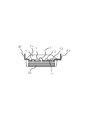
図2は、本発明の実施形態にかかる半導体モジュールにおける熱の流れを模式的に示す図であって、特に半導体モジュール51を電力変換機器101に組み込んだ場合について説明するものである。
図2は、本発明の実施形態にかかる半導体モジュールにおける熱の流れを模式的に示す図であって、特に半導体モジュール51を電力変換機器101に組み込んだ場合について説明するものである。
図2において、半導体モジュール51は冷却用ヒートシンク102上に放熱用絶縁層2が当接するようにして搭載されるとともに、外部接続リードフレーム9が半導体モジュール51の上部に配置されたプリント配線板部111に接続されて、電力変換機器101を構成している。
電力変換機器101では、半導体モジュール51におけるパワー半導体素子7により主回路が構成されるとともに、プリント配線板部111におけるプリント配線板114に実装された電子回路部品115a,115b,115cなどにより、その他の電源回路や制御用の回路が構成されている。電子回路部品115a,115b,115cとしては例えばIC、LSI、抵抗、コンデンサ、リアクトルなどの各種部品が用いられる。
図2では一部分だけが図示されているプリント配線板114はプリント基板本体112に回路パターン113が形成されたものであり、このプリント配線板114に電子回路部品115a,115b,115cなどがはんだ116による接合で実装されて、プリント配線板部111を構成している。半導体モジュール51の外部接続用リードフレーム9はプリント配線板114の挿入孔118に挿入されて回路パターン113にはんだ117による接合で接続される。
なお、本発明の実施形態にかかる半導体モジュールとプリント配線板部との接続構造は図2に示された構成に限定されるものではない。
また、図2において、半導体モジュール51におけるパワー半導体素子7として例えばIGBT(Insulated Gate
Bipolar Transistor)を実装した構成では、IGBTの下面のコレクタ電極が金属ブロック1の第2面1bに接合され、IGBTの上面に形成されているエミッタ電極とゲート電極とがそれぞれボンディングワイヤ11aにより中継電極3に接続される。
また、図2において、半導体モジュール51におけるパワー半導体素子7として例えばIGBT(Insulated Gate
Bipolar Transistor)を実装した構成では、IGBTの下面のコレクタ電極が金属ブロック1の第2面1bに接合され、IGBTの上面に形成されているエミッタ電極とゲート電極とがそれぞれボンディングワイヤ11aにより中継電極3に接続される。
図2において、半導体モジュール51におけるパワー半導体素子7が動作時に発熱した場合の熱の流れを白抜き矢印h1~h5により模式的に示している。白抜き矢印h1~h5の幅は流れる熱量の大小を定性的に示している。なお、図2では、パワー半導体素子7から左側のボンディングワイヤ11aに沿って流れる熱の流れのみを示している。また、図2では、説明の便宜上、パワー半導体素子7と中継電極3とを接続するボンディングワイヤを11aとし、中継電極3と外部接続用リードフレーム9とを接続するボンディングワイヤを11bとしている。
図2において、半導体モジュール51内のパワー半導体素子7が動作時に発生する熱は、パワー半導体素子7からはんだ層23、金属ブロック1および放熱用絶縁層2を介して冷却用ヒートシンク102に伝達されるとともに、パワー半導体素子7からボンディングワイヤ11aを介して外部接続用リードフレーム9側にも伝達される。しかしながら、本発明による半導体モジュール51では、金属ブロック1上に中継電極用絶縁層4を介して形成された中継電極3を備え、パワー半導体素子7からのボンディングワイヤ11aを中継電極3に接合した上で、中継電極3から別のボンディングワイヤ11bを介して外部接続用リードフレーム9に接続するようにしている。このため、半導体モジュール51では、パワー半導体素子7からボンディングワイヤ11aを経由して流れてくる熱は大部分が中継電極3、熱伝導性に優れたセラミックス材料からなる中継電極用絶縁層4および金属ブロック1を介して冷却用ヒートシンク102に伝達され、中継電極3からボンディングワイヤ11bを介して外部接続用リードフレーム9側に伝達される熱量は十分に小さく抑制されたものとなる。これにより、半導体モジュール51の外部接続用リードフレーム9と接続されるプリント配線板部111側に伝わる熱量を抑制することができ、プリント配線板部111を形成するプリント配線板114に対する加熱を効果的に抑制することができる。
なお、上述のような半導体モジュール51は、図2に示されるように、パワー半導体素子7が動作時に発生する熱を、パワー半導体素子7→はんだ層23→金属ブロック1といいう第1の伝熱経路と、パワー半導体素子7→ボンディングワイヤ11a→中継電極3→中継電極用絶縁層4→金属ブロック1という第2伝熱経路との2つの伝熱経路で効率良く金属ブロック1に伝達できるので、熱容量が高く放熱性に優れた金属ブロック1の機能をより有効に生かしたものとなっている。
図2において、半導体モジュール51内のパワー半導体素子7が動作時に発生する熱は、パワー半導体素子7からはんだ層23、金属ブロック1および放熱用絶縁層2を介して冷却用ヒートシンク102に伝達されるとともに、パワー半導体素子7からボンディングワイヤ11aを介して外部接続用リードフレーム9側にも伝達される。しかしながら、本発明による半導体モジュール51では、金属ブロック1上に中継電極用絶縁層4を介して形成された中継電極3を備え、パワー半導体素子7からのボンディングワイヤ11aを中継電極3に接合した上で、中継電極3から別のボンディングワイヤ11bを介して外部接続用リードフレーム9に接続するようにしている。このため、半導体モジュール51では、パワー半導体素子7からボンディングワイヤ11aを経由して流れてくる熱は大部分が中継電極3、熱伝導性に優れたセラミックス材料からなる中継電極用絶縁層4および金属ブロック1を介して冷却用ヒートシンク102に伝達され、中継電極3からボンディングワイヤ11bを介して外部接続用リードフレーム9側に伝達される熱量は十分に小さく抑制されたものとなる。これにより、半導体モジュール51の外部接続用リードフレーム9と接続されるプリント配線板部111側に伝わる熱量を抑制することができ、プリント配線板部111を形成するプリント配線板114に対する加熱を効果的に抑制することができる。
なお、上述のような半導体モジュール51は、図2に示されるように、パワー半導体素子7が動作時に発生する熱を、パワー半導体素子7→はんだ層23→金属ブロック1といいう第1の伝熱経路と、パワー半導体素子7→ボンディングワイヤ11a→中継電極3→中継電極用絶縁層4→金属ブロック1という第2伝熱経路との2つの伝熱経路で効率良く金属ブロック1に伝達できるので、熱容量が高く放熱性に優れた金属ブロック1の機能をより有効に生かしたものとなっている。
次に、図11は、比較例として、従来技術による半導体モジュールにおける熱の流れを模式的に示す図であって、特に、図10で説明した構成の半導体モジュールを半導体モジュール151として、この半導体モジュール151を電力変換機器201に組み込んだ場合について説明するものである。
図11において、半導体モジュール151は冷却用ヒートシンク202上に放熱用絶縁層2が当接するようにして搭載されるとともに、外部接続用リードフレーム9が半導体モジュール151の上部に配置されたプリント配線板部111Aに接続されて、電力変換機器201を構成している。なお、プリント配線板部111Aの構成は、回路パターンおよび電子回路部品の配置が半導体モジュール151における外部接続用リードフレーム9の配置に対応したものとなっている点以外は、図2に示したプリント配線板部111と同様である。また、図11における半導体モジュール151とプリント配線板部111Aとの接続構造は、図2における半導体モジュール51とプリント配線板部111との接続構造と同様である。
図11において、半導体モジュール151におけるパワー半導体素子7が動作時に発熱した場合の熱の流れを白抜き矢印h11~h13により模式的に示している。白抜き矢印h11~h13の幅は流れる熱量の大小を定性的に示している。なお、図11では、パワー半導体素子7から左側のボンディングワイヤ11に沿って流れる熱の流れのみを示している。
図11において、半導体モジュール151内のパワー半導体素子7が動作時に発生する熱は、パワー半導体素子7からはんだ層23、金属ブロック1および放熱用絶縁層2を介して冷却用ヒートシンク202に伝達されるとともに、パワー半導体素子7からボンディングワイヤ11を介して外部接続用リードフレーム9側にも伝達される。
従来技術による半導体モジュール151では、パワー半導体素子7からのボンディングワイヤ11を直接外部接続用リードフレーム9に接続するようにしているので、パワー半導体素子7からボンディングワイヤ11を経由して流れてくる熱はそのまま外部接続用リードフレーム9を流れていく。これにより、半導体モジュール151では、半導体モジュール151の外部接続用リードフレーム9と接続されるプリント配線板部111A側に伝わる熱量を抑制することができないため、プリント配線板部111Aを形成するプリント配線板114Aに対する加熱を抑制することができない。
図11において、半導体モジュール151内のパワー半導体素子7が動作時に発生する熱は、パワー半導体素子7からはんだ層23、金属ブロック1および放熱用絶縁層2を介して冷却用ヒートシンク202に伝達されるとともに、パワー半導体素子7からボンディングワイヤ11を介して外部接続用リードフレーム9側にも伝達される。
従来技術による半導体モジュール151では、パワー半導体素子7からのボンディングワイヤ11を直接外部接続用リードフレーム9に接続するようにしているので、パワー半導体素子7からボンディングワイヤ11を経由して流れてくる熱はそのまま外部接続用リードフレーム9を流れていく。これにより、半導体モジュール151では、半導体モジュール151の外部接続用リードフレーム9と接続されるプリント配線板部111A側に伝わる熱量を抑制することができないため、プリント配線板部111Aを形成するプリント配線板114Aに対する加熱を抑制することができない。
これに対して、本発明による半導体モジュールでは、上述のように、電力変換機器などの電気機器に組み込まれた状態において、半導体モジュール内のパワー半導体素子が動作時に発生する熱のうち、半導体モジュールに接続されたプリント配線板部側に伝わる熱量を抑制し、プリント配線板などに対する加熱を効果的に抑制することができる。
次に、図1に戻って、図1(b)~図1(c)の構成例について説明する。
図1(b)に示す半導体モジュール51Aは、上述の図1(a)に示した半導体モジュール51に対して、中継電極3と外部接続リードフレーム9とをボンディングワイヤ11bで接続する代わりに、外部接続リードフレーム9Aを中継電極3に直接接合するようにした点が異なるものであり、それ以外の点は同様である。
図1(b)に示す半導体モジュール51Aは、上述の図1(a)に示した半導体モジュール51に対して、中継電極3と外部接続リードフレーム9とをボンディングワイヤ11bで接続する代わりに、外部接続リードフレーム9Aを中継電極3に直接接合するようにした点が異なるものであり、それ以外の点は同様である。
図1(c)に示す半導体モジュール51Bは、上述の図1(b)に示した半導体モジュール51Aに対して、パワー半導体素子7と中継電極3とをボンディングワイヤ11aで接続する代わりに、リードフレーム13で接続するようにした点が異なるものであり、それ以外の点は同様である。
続いて、本発明の実施形態にかかる半導体モジュールの製造方法について図3ないし図5を参照して説明する。図3ないし図5は、本発明の実施形態にかかる半導体モジュールの製造工程における各段階の構造を示す断面図であり、特に図1(a)に示した半導体モジュール51を対象として説明するものである。
最初に、1.0~4.0mm程度の銅板を、プレス加工により、正方形または長方形に打ち抜いて、金属ブロック1を製作する(図3(a))。
次に、マスク21をあてて、溶射法もしくはエアロゾルデポジション法により例えば酸化アルミニウム粉などのセラミックス粉末22を積層することにより、金属ブロック1の第1面1a側に放熱用絶縁層2を形成する。
次に、マスク21をあてて、溶射法もしくはエアロゾルデポジション法により例えば酸化アルミニウム粉などのセラミックス粉末22を積層することにより、金属ブロック1の第1面1a側に放熱用絶縁層2を形成する。
放熱用絶縁層2としては、金属ブロック1の第1面1aに第1面部絶縁層2aを形成するとともに金属ブロック1の側面1cの一部に側面部絶縁層2bを形成する。側面部絶縁層2bは第1面部絶縁層2aにつながるように形成する(図3(b)~図3(c))。
溶射法のうち、例えばプラスマ溶射法で金属ブロック1の第1面1a側に絶縁層を形成する場合は、セラミックス粉末には酸化珪素、酸化アルミニウム、窒化珪素、窒化アルミニウム、窒化ホウ素からなる1種類以上を用いる。雰囲気としては大気圧もしくは減圧下でマスク21を介して金属ブロック1に溶射を行い、放熱用絶縁層2を堆積させる。
なお、プラスマ溶射法により金属ブロック1上に放熱用絶縁層2として第1面部絶縁層2aに加えて側面部絶縁層2bも形成するため、例えば図3(b)に示すように金属ブロック1の側面1cの一部をマスク21から露出させた状態で、セラミックス粉末を原料粉末22及び22Aとして溶射する。この際、(図示されない)溶射ノズルの方向を調整して、金属ブロック1の第1面1aに正対する原料粉末22の方向に加えて斜め方向の原料粉末22Aも利用することによって、金属ブロック1上に、第1面1aの第1面部絶縁層2aに加えて、側面1cの一部にも第1面部絶縁層2aとつながる側面部絶縁層2bを形成する。金属ブロック1の側面1cのうち、側面部絶縁層2bによって覆う範囲は、金属ブロック1と図示しない外部の冷却用ヒートシンクとの間に生じ得る電位差などの絶縁設計条件を勘案して決定される。
放熱用絶縁層2の厚みは溶射時間をコントロールすることにより調整できる。絶縁層の厚みは10~500μmが好ましい。上記のようにして形成された放熱用絶縁層2は、絶縁特性として、例えば厚み200μmで交流破壊電圧5kV以上を有しており、耐電圧定格が1200Vのパワー素子にも用いることができる。
次に、エアロゾルデポジション法で金属ブロック1の第1面1a側に放熱用絶縁層2を堆積させる場合について説明する。エアロゾルデポジション法とは、微粒子あるいは超微粒子原料をガスと混合してエアロゾル化し、ノズルを通して基板に皮膜を形成する技術である。ガスにはヘリウムもしくは空気が用いられる。装置は、図示しないエアロゾル化チャンバーと成膜チャンバーから構成することができる。成膜チャンバーは、真空ポンプで50Pa~1kPa前後に減圧する。原料である微粒子または超微粒子材料は乾燥された状態でエアロゾル化チャンバー内でガスと攪拌・混合してエアロゾル化され、両チャンバーの圧力差により生じるガスの流れにより成膜チャンバーに搬送され、スリット状のノズルを通過することで加速され、成膜対象である金属ブロック1の第1面1a側に噴射される。原料微粒子には、機械的に粒径0.1~2μmに粉砕したセラミックス粉末を用いる。ガス搬送された超微粒子は、減圧されたチャンバー内の微小開口のノズルを通すことで数百m/secまで加速される。成膜速度や成膜体の密度は使用されるセラミックス微粒子の粒径や凝集状態、乾燥状態などに大きく依存するため、エアロゾル化チャンバーと成膜チャンバーとの間に凝集粒子の解砕器や分級装置を用いている。
そして、放熱用絶縁層2を膜として形成するためには、粒径0.1~2μmの微粒子のセラミックスを高速で基板上に吹き付け、その時の衝突エネルギーにて10~30nm前後の微結晶粒子に破砕され、新生面が形成されて表面が活性化され、粒子同士が結合されることで、ち密なナノ結晶組織のセラミックス膜が形成される。また、エアロゾルデポジション法では特に温度をかけることなく常温でセラミックス膜を形成可能である。
エアロゾルデポジションの微粒子には、粒子径が0.1~2μm程度の酸化アルミニウム、窒化珪素、窒化アルミニウム、窒化ホウ素のいずれかを用いることが好ましい。必要な膜厚を得るため、所定の時間、マスク21を用い微粒子を吹き付け、図3(c)に示す放熱用絶縁層2を形成する。
なお、エアロゾルデポジション法により金属ブロック1上に絶縁層2として第1面部絶縁層2aに加えて側面部絶縁層2bも形成するため、上述のプラスマ溶射法の場合と同様に、例えば図3(b)に示すように金属ブロック1の側面1cの一部をマスク21から露出させた状態で、セラミックス微粒子を原料粉末22及び22Aとして吹き付ける。この際、(図示されない)ノズルの方向を調整して、金属ブロック1の第1面1aに正対する原料粉末22の方向に加えて斜め方向の原料粉末22Aも利用することによって、金属ブロック1上に、第1面1aの第1面部絶縁層2aに加えて、側面1cの一部にも第1面部絶縁層2aとつながる側面部絶縁層2bを形成する。金属ブロック1の側面1cのうち、側面部絶縁層2bによって覆う範囲は、金属ブロック1と図示しない外部の冷却用ヒートシンクとの間に生じ得る電位差など絶縁設計条件を勘案して決定される。
ここで、微粒子には窒化珪素、窒化アルミニウム、窒化ホウ素いずれかのフィラーに酸化アルミニウムの皮膜を形成したもの、もしくは、窒化珪素、窒化アルミニウム、窒化ホウ素いずれかのフィラーに酸化珪素の皮膜を形成したものも適用可能である。これらの微粒子を用いれば、2種類以上のセラミックスを複合した絶縁層が形成できる。
放熱用絶縁層2の厚みは、溶射法と同様の10~500μmが好ましい。上記のようにして形成された絶縁層2は、絶縁特性として、例えば厚み200μmで交流破壊電圧5kV以上を有しており、耐電圧定格が1200Vのパワー素子にも用いることができる。
次に、金属ブロック1の第2面1bにもマスク21Aをあてて、溶射法もしくはエアロゾルデポジション法により例えば酸化アルミニウム粉などのセラミックス粉末22を積層することにより、金属ブロック1の第2面1b側に中継電極用絶縁層4を形成する(図3(d)~図4(a))。この中継電極用絶縁層2は金属ブロック1の第2面1bにおける全面ではなく一部分に形成する。
中継電極用絶縁層4の形成に用いるセラミックス微粒子の材料、および絶縁層の形成方法は、溶射法もしくはエアロゾルデポジション法とも上述の放熱用絶縁層2と同様である。
中継電極用絶縁層2の厚みは、溶射法またはエアロゾルデポジション法のいずれで形成したものでも、放熱用絶縁層2と同様に10~500μmが好ましい。
次に、中継電極用絶縁層4の上に銅製の中継電極3を積層する。銅を堆積させる方法は、絶縁層と同様にプラズマ溶射法を用いる。すなわち、金属ブロック1の第2面1bに形成されている中継電極用絶縁層4にマスク21Bをあてて、銅粒子24を溶射し、中継電極3を形成する(図4(b)~(c))。
これにより、金属ブロック1の第1面1a側に放熱用絶縁層2が形成されるとともに、第2面1bの一部には中継電極3が中継電極用絶縁層4を介して形成された絶縁金属ブロック5が完成する(図4(d))。
次に、絶縁金属ブロック5における金属ブロック1の第2面1bにパワー半導体素子7をはんだ23での接合により接合する(図5(a))。はんだ付けは、ペレット状のはんだを利用し、水素還元が可能な炉において行なう。水素還元が可能な炉を使うのは、金属ブロック1の表面の酸化膜を水素還元により除去し、活性化させることにより、はんだとの濡れ性を向上させるためである。はんだ材料には例えば、SnPbAgからなる高温はんだ、SnAgCu系からなる鉛フリーはんだを用いる。はんだ付けの温度は、はんだの融点に応じて設定される。
パワー半導体素子7と金属ブロック1との間のはんだ層23にボイドが残留すると、熱抵抗が高くなり、パワー半導体素子7から生じる熱を効率よく放熱することができない。そこで、ボイドを発生しないように、はんだが溶融している状態で、1.3kPa(10Torr)以下の真空引きを行なう。
次に、ボンディングワイヤ11aによりパワー半導体素子7と中継電極3との接続を行なう(図5(b))。ボンディングワイヤ11aは、線径が125~500μmのAlワイヤを使用して超音波接合する。なお、パワー半導体素子7と中継電極3との接続には、ボンディングワイヤ11aの代わりに、図1(c)に示したようにリードフレーム13を使用しても良い。
さらに、ボンディングワイヤ11bにより中継電極3と外部リード端子9との接続を行なう(図5(c))。ボンディングワイヤ11bは、上述のボンディングワイヤ11aと同様に線径が125~500μmのAlワイヤを使用して超音波接合する。なお、中継電極3と外部接続用リードフレーム9との接続には、ボンディングワイヤ11bの代わりに、図1(c)に示したリードフレーム13と同様なリードフレームを使用しても良く、さらには、図1(b)~(c)に示したように中継電極3に外部接続用リードフレーム9を直接接合しても良い。
次に、図5(c)に示した組立体を、トランスファー成形機に取り付けられた金型にセットする。金型は170~180℃程度に保温されており、予熱後にタブレット状のエポキシ樹脂14をプランジャーにて金型内に流し込む。エポキシ樹脂14は、酸化珪素、酸化アルミニウム、窒化珪素、窒化アルミニウム、窒化ホウ素からなるフィラー群の1種類以上を含むエポキシ樹脂からなり、熱伝導率は0.5~5W/m・Kの樹脂を用いる。
次に、中継電極用絶縁層4の上に銅製の中継電極3を積層する。銅を堆積させる方法は、絶縁層と同様にプラズマ溶射法を用いる。すなわち、金属ブロック1の第2面1bに形成されている中継電極用絶縁層4にマスク21Bをあてて、銅粒子24を溶射し、中継電極3を形成する(図4(b)~(c))。
これにより、金属ブロック1の第1面1a側に放熱用絶縁層2が形成されるとともに、第2面1bの一部には中継電極3が中継電極用絶縁層4を介して形成された絶縁金属ブロック5が完成する(図4(d))。
次に、絶縁金属ブロック5における金属ブロック1の第2面1bにパワー半導体素子7をはんだ23での接合により接合する(図5(a))。はんだ付けは、ペレット状のはんだを利用し、水素還元が可能な炉において行なう。水素還元が可能な炉を使うのは、金属ブロック1の表面の酸化膜を水素還元により除去し、活性化させることにより、はんだとの濡れ性を向上させるためである。はんだ材料には例えば、SnPbAgからなる高温はんだ、SnAgCu系からなる鉛フリーはんだを用いる。はんだ付けの温度は、はんだの融点に応じて設定される。
パワー半導体素子7と金属ブロック1との間のはんだ層23にボイドが残留すると、熱抵抗が高くなり、パワー半導体素子7から生じる熱を効率よく放熱することができない。そこで、ボイドを発生しないように、はんだが溶融している状態で、1.3kPa(10Torr)以下の真空引きを行なう。
次に、ボンディングワイヤ11aによりパワー半導体素子7と中継電極3との接続を行なう(図5(b))。ボンディングワイヤ11aは、線径が125~500μmのAlワイヤを使用して超音波接合する。なお、パワー半導体素子7と中継電極3との接続には、ボンディングワイヤ11aの代わりに、図1(c)に示したようにリードフレーム13を使用しても良い。
さらに、ボンディングワイヤ11bにより中継電極3と外部リード端子9との接続を行なう(図5(c))。ボンディングワイヤ11bは、上述のボンディングワイヤ11aと同様に線径が125~500μmのAlワイヤを使用して超音波接合する。なお、中継電極3と外部接続用リードフレーム9との接続には、ボンディングワイヤ11bの代わりに、図1(c)に示したリードフレーム13と同様なリードフレームを使用しても良く、さらには、図1(b)~(c)に示したように中継電極3に外部接続用リードフレーム9を直接接合しても良い。
次に、図5(c)に示した組立体を、トランスファー成形機に取り付けられた金型にセットする。金型は170~180℃程度に保温されており、予熱後にタブレット状のエポキシ樹脂14をプランジャーにて金型内に流し込む。エポキシ樹脂14は、酸化珪素、酸化アルミニウム、窒化珪素、窒化アルミニウム、窒化ホウ素からなるフィラー群の1種類以上を含むエポキシ樹脂からなり、熱伝導率は0.5~5W/m・Kの樹脂を用いる。
エポキシ樹脂14の注入を行なうと数十秒で硬化するので、直ぐに金型から取り出し、恒温槽で後硬化を行なって封止を完了する(図5(d))。
図6は本発明の実施形態にかかる半導体モジュールの異なる構成例を示す断面図である。本発明による半導体モジュールは、金属ブロック1と図示しない外部の冷却用ヒートシンクとの間に生じ得る電位差など絶縁設計条件との関係で問題のない場合には、図6(a)~図6(c)に示す半導体モジュール51C、51D、51Eのように、放熱用絶縁層2が第1面にのみ形成された構成であってもよい。半導体モジュール51C、51D、51Eの各構成は、上記以外の点では、図1(a)~図1(c)に示した半導体モジュール51、51A、51Bの各構成にそれぞれ対応している。
以上説明した本発明による半導体モジュールでは、特に、金属ブロックの第2面に接合されたパワー半導体素子など回路素子からのボンディングワイヤまたはリードフレームを中継電極に接合した上で、この中継電極と外部リード端子とを接続していることにより、回路素子が動作時に発生し、回路素子からのボンディングワイヤまたはリードフレームに沿って伝達される熱は、主に中継電極および熱伝導性に優れたセラミックス材料からなる中継電極用絶縁層を介して熱容量が高く放熱性に優れた金属ブロックの方に伝わるので、外部リード端子の方に伝わる熱量は十分に抑制することができる。
これにより、本発明による半導体モジュールでは、その外部リード端子から当該外部リード端子に接続された外部の例えばプリント基板などに流れ出す熱量を効果的に抑制することができるため、外部のプリント基板などに対する加熱を効果的に抑制することができるので、このような半導体モジュールを用いることによって、電力変換機器の寸法増大やコスト増大なしに電力変換機器のケース内の温度上昇を効果的に抑制することができる。
図6は本発明の実施形態にかかる半導体モジュールの異なる構成例を示す断面図である。本発明による半導体モジュールは、金属ブロック1と図示しない外部の冷却用ヒートシンクとの間に生じ得る電位差など絶縁設計条件との関係で問題のない場合には、図6(a)~図6(c)に示す半導体モジュール51C、51D、51Eのように、放熱用絶縁層2が第1面にのみ形成された構成であってもよい。半導体モジュール51C、51D、51Eの各構成は、上記以外の点では、図1(a)~図1(c)に示した半導体モジュール51、51A、51Bの各構成にそれぞれ対応している。
以上説明した本発明による半導体モジュールでは、特に、金属ブロックの第2面に接合されたパワー半導体素子など回路素子からのボンディングワイヤまたはリードフレームを中継電極に接合した上で、この中継電極と外部リード端子とを接続していることにより、回路素子が動作時に発生し、回路素子からのボンディングワイヤまたはリードフレームに沿って伝達される熱は、主に中継電極および熱伝導性に優れたセラミックス材料からなる中継電極用絶縁層を介して熱容量が高く放熱性に優れた金属ブロックの方に伝わるので、外部リード端子の方に伝わる熱量は十分に抑制することができる。
これにより、本発明による半導体モジュールでは、その外部リード端子から当該外部リード端子に接続された外部の例えばプリント基板などに流れ出す熱量を効果的に抑制することができるため、外部のプリント基板などに対する加熱を効果的に抑制することができるので、このような半導体モジュールを用いることによって、電力変換機器の寸法増大やコスト増大なしに電力変換機器のケース内の温度上昇を効果的に抑制することができる。
1:金属ブロック
1a:第1面
1b:第2面
1c:側面
2:放熱用絶縁層
2a:第1面部絶縁層
2b:側面部絶縁層
3:中継電極
4:中継電極用絶縁層
5:絶縁金属ブロック
7:パワー半導体素子
9,9A,9B,9C,9D,9E,9F:外部接続用リードフレーム
11,11a,11b:ボンディングワイヤ
12:IC用ボンディングワイヤ
13:リードフレーム
14:成形樹脂(エポキシ樹脂)
21,21A,21B:マスク
22,22A:セラミックス粒子
23:はんだ
24:銅粒子
31:駆動IC
32:ヒートシンク
33:絶縁基板
34:金属板
35:銅箔
36:絶縁層
37:絶縁金属ブロック
51,51A,51B,51C,51D,51E:半導体モジュール
101:電力変換機器
102:冷却用ヒートシンク
111,111A:プリント配線板部
112,112A:プリント基板本体
113,113A:回路パターン
114,114A:プリント配線板
115a,115b,115c:電子回路部品
116:はんだ
117:はんだ
118:挿入孔
151:半導体モジュール
201:電力変換機器
202:冷却用ヒートシンク
h1,h2,h3,h4,h5,h11,h12,h13:熱の流れ
1a:第1面
1b:第2面
1c:側面
2:放熱用絶縁層
2a:第1面部絶縁層
2b:側面部絶縁層
3:中継電極
4:中継電極用絶縁層
5:絶縁金属ブロック
7:パワー半導体素子
9,9A,9B,9C,9D,9E,9F:外部接続用リードフレーム
11,11a,11b:ボンディングワイヤ
12:IC用ボンディングワイヤ
13:リードフレーム
14:成形樹脂(エポキシ樹脂)
21,21A,21B:マスク
22,22A:セラミックス粒子
23:はんだ
24:銅粒子
31:駆動IC
32:ヒートシンク
33:絶縁基板
34:金属板
35:銅箔
36:絶縁層
37:絶縁金属ブロック
51,51A,51B,51C,51D,51E:半導体モジュール
101:電力変換機器
102:冷却用ヒートシンク
111,111A:プリント配線板部
112,112A:プリント基板本体
113,113A:回路パターン
114,114A:プリント配線板
115a,115b,115c:電子回路部品
116:はんだ
117:はんだ
118:挿入孔
151:半導体モジュール
201:電力変換機器
202:冷却用ヒートシンク
h1,h2,h3,h4,h5,h11,h12,h13:熱の流れ
Claims (9)
- 第1面および第2面を有する金属ブロックと、
前記金属ブロックの少なくとも第1面に直接セラミックス材料を積層して形成された放熱用絶縁層と、
前記金属ブロックの第2面の一部分に直接セラミックス材料を積層して形成された中継電極用絶縁層と、
前記中継電極用絶縁層の上面に金属材料を積層して形成された中継電極と、
前記金属ブロックの第2面に接合された回路素子と、
外部リード端子とを備え、
前記回路素子からのボンディングワイヤまたはリードフレームを前記中継電極に接合するとともに、
前記中継電極と前記外部リード端子とを接続した
ことを特徴とする半導体モジュール。 - 請求項1に記載の半導体モジュールにおいて、
前記放熱用絶縁層は、前記金属ブロックの第1面に連接する側面の少なくとも一部を覆うことを特徴とする半導体モジュール。 - 請求項1に記載の半導体モジュールにおいて、
前記放熱用絶縁層および前記中継電極用絶縁層は、熱伝導率が1~200W/m・Kであり、かつ厚さが10~500μmであることを特徴とする半導体モジュール。 - 請求項1に記載の半導体モジュールにおいて、
前記放熱用絶縁層および前記中継電極用絶縁層は、酸化珪素、酸化アルミニウム、窒化珪素、窒化アルミニウム、窒化ホウ素からなるフィラー群の少なくとも1種類からなることを特徴とする半導体モジュール。 - 請求項4に記載の半導体モジュールにおいて、
前記放熱用絶縁層および前記中継電極用絶縁層は、前記フィラー群の少なくとも1種によるセラミックス微粒子をプラズマ溶射法にて堆積させることにより形成したことを特徴とする半導体モジュール。 - 請求項4に記載の半導体モジュールにおいて、
前記放熱用絶縁層および前記中継電極用絶縁層は、前記フィラー群の少なくとも1種によるセラミックス微粒子をエアロゾルデポジション法にて堆積させることにより形成したことを特徴とする半導体モジュール。 - 請求項1から6のいずれか1項に記載の半導体モジュールにおいて、
前記中継電極は、金属材料として銅粒子を溶射して形成したことを特徴とする半導体モジュール。 - 請求項1から6のいずれか1項に記載の半導体モジュールにおいて、
前記中継電極と外部リード端子とをボンディングワイヤまたはリードフレームを介して接続したことを特徴とする半導体モジュール。 - 請求項1から6のいずれか1項に記載の半導体モジュールにおいて、
前記回路素子は、パワー半導体素子であることを特徴とする半導体モジュール。
Priority Applications (2)
| Application Number | Priority Date | Filing Date | Title |
|---|---|---|---|
| JP2014525710A JP6024750B2 (ja) | 2012-07-17 | 2013-07-11 | 半導体モジュール |
| US14/512,368 US9245832B2 (en) | 2012-07-17 | 2014-10-10 | Semiconductor module |
Applications Claiming Priority (2)
| Application Number | Priority Date | Filing Date | Title |
|---|---|---|---|
| JP2012-158288 | 2012-07-17 | ||
| JP2012158288 | 2012-07-17 |
Related Child Applications (1)
| Application Number | Title | Priority Date | Filing Date |
|---|---|---|---|
| US14/512,368 Continuation US9245832B2 (en) | 2012-07-17 | 2014-10-10 | Semiconductor module |
Publications (1)
| Publication Number | Publication Date |
|---|---|
| WO2014013705A1 true WO2014013705A1 (ja) | 2014-01-23 |
Family
ID=49948548
Family Applications (1)
| Application Number | Title | Priority Date | Filing Date |
|---|---|---|---|
| PCT/JP2013/004300 Ceased WO2014013705A1 (ja) | 2012-07-17 | 2013-07-11 | 半導体モジュール |
Country Status (3)
| Country | Link |
|---|---|
| US (1) | US9245832B2 (ja) |
| JP (1) | JP6024750B2 (ja) |
| WO (1) | WO2014013705A1 (ja) |
Cited By (2)
| Publication number | Priority date | Publication date | Assignee | Title |
|---|---|---|---|---|
| WO2018131310A1 (ja) * | 2017-01-13 | 2018-07-19 | 三菱電機株式会社 | 電力用半導体装置及び電力用半導体装置の製造方法 |
| JP2019121612A (ja) * | 2017-12-28 | 2019-07-22 | 新電元工業株式会社 | 電子デバイス |
Families Citing this family (10)
| Publication number | Priority date | Publication date | Assignee | Title |
|---|---|---|---|---|
| JP6699111B2 (ja) * | 2015-08-18 | 2020-05-27 | 富士電機株式会社 | 半導体装置及び半導体装置の製造方法 |
| DE102015122259B4 (de) * | 2015-12-18 | 2020-12-24 | Infineon Technologies Austria Ag | Halbleitervorrichtungen mit einer porösen Isolationsschicht |
| KR102239069B1 (ko) | 2016-03-01 | 2021-04-12 | 닛폰세이테츠 가부시키가이샤 | 세라믹스 적층체 |
| US20180222807A1 (en) * | 2017-02-03 | 2018-08-09 | Rolls-Royce Corporation | Increasing the density of a bond coat |
| US20190300999A1 (en) * | 2018-04-02 | 2019-10-03 | Tokyo Electron Limited | Method of forming metallic film |
| JP7147502B2 (ja) * | 2018-11-19 | 2022-10-05 | 三菱電機株式会社 | 半導体装置、電力変換装置および半導体装置の製造方法 |
| US11901341B2 (en) * | 2018-11-26 | 2024-02-13 | Mitsubishi Electric Corporation | Semiconductor package and production method thereof, and semiconductor device |
| DE102019206523A1 (de) * | 2019-05-07 | 2020-11-12 | Zf Friedrichshafen Ag | Leistungsmodul mit gehäusten Leistungshalbleitern zur steuerbaren elektrischen Leistungsversorgung eines Verbrauchers |
| JP7196815B2 (ja) | 2019-10-23 | 2022-12-27 | 三菱電機株式会社 | 半導体モジュール及び電力変換装置 |
| US11862688B2 (en) * | 2021-07-28 | 2024-01-02 | Apple Inc. | Integrated GaN power module |
Citations (4)
| Publication number | Priority date | Publication date | Assignee | Title |
|---|---|---|---|---|
| JPS5536915A (en) * | 1978-09-04 | 1980-03-14 | Hitachi Ltd | Electronic circuit and its manufacturing |
| JPH05109940A (ja) * | 1991-10-21 | 1993-04-30 | Sanyo Electric Co Ltd | 混成集積回路 |
| JP2000156439A (ja) * | 1998-11-20 | 2000-06-06 | Mitsubishi Electric Corp | パワー半導体モジュール |
| JP2011114010A (ja) * | 2009-11-24 | 2011-06-09 | Fuji Electric Holdings Co Ltd | 半導体モジュールおよびその製造方法ならびに電気機器 |
Family Cites Families (9)
| Publication number | Priority date | Publication date | Assignee | Title |
|---|---|---|---|---|
| JPS56100436A (en) * | 1980-01-17 | 1981-08-12 | Toshiba Corp | Manufacture of semiconductor element |
| JPS61237459A (ja) * | 1985-04-12 | 1986-10-22 | Sumitomo Electric Ind Ltd | 半導体装置用リ−ドフレ−ム |
| JPH05226560A (ja) * | 1991-10-18 | 1993-09-03 | Toppan Printing Co Ltd | 半導体装置用リードフレームの製造方法 |
| JP3516789B2 (ja) | 1995-11-15 | 2004-04-05 | 三菱電機株式会社 | 半導体パワーモジュール |
| JPH09275676A (ja) | 1996-04-01 | 1997-10-21 | Nissan Motor Co Ltd | Dc−dcコンバータ |
| JP3918724B2 (ja) * | 2002-11-28 | 2007-05-23 | トヨタ自動車株式会社 | ワイヤが接合されている半導体装置の製造方法 |
| DE102005016830A1 (de) * | 2004-04-14 | 2005-11-03 | Denso Corp., Kariya | Halbleitervorrichtung und Verfahren zu ihrer Herstellung |
| JP2007305772A (ja) * | 2006-05-11 | 2007-11-22 | Fuji Electric Device Technology Co Ltd | 半導体装置および半導体装置の製造方法 |
| EP2650915B1 (en) * | 2010-12-10 | 2017-07-26 | Panasonic Intellectual Property Management Co., Ltd. | Conducting path and semiconductor device |
-
2013
- 2013-07-11 WO PCT/JP2013/004300 patent/WO2014013705A1/ja not_active Ceased
- 2013-07-11 JP JP2014525710A patent/JP6024750B2/ja active Active
-
2014
- 2014-10-10 US US14/512,368 patent/US9245832B2/en active Active
Patent Citations (4)
| Publication number | Priority date | Publication date | Assignee | Title |
|---|---|---|---|---|
| JPS5536915A (en) * | 1978-09-04 | 1980-03-14 | Hitachi Ltd | Electronic circuit and its manufacturing |
| JPH05109940A (ja) * | 1991-10-21 | 1993-04-30 | Sanyo Electric Co Ltd | 混成集積回路 |
| JP2000156439A (ja) * | 1998-11-20 | 2000-06-06 | Mitsubishi Electric Corp | パワー半導体モジュール |
| JP2011114010A (ja) * | 2009-11-24 | 2011-06-09 | Fuji Electric Holdings Co Ltd | 半導体モジュールおよびその製造方法ならびに電気機器 |
Cited By (5)
| Publication number | Priority date | Publication date | Assignee | Title |
|---|---|---|---|---|
| WO2018131310A1 (ja) * | 2017-01-13 | 2018-07-19 | 三菱電機株式会社 | 電力用半導体装置及び電力用半導体装置の製造方法 |
| JPWO2018131310A1 (ja) * | 2017-01-13 | 2019-04-25 | 三菱電機株式会社 | 電力用半導体装置及び電力用半導体装置の製造方法 |
| US12232300B2 (en) | 2017-01-13 | 2025-02-18 | Mitsubishi Electric Corporation | Power semiconductor device and method for manufacturing power semiconductor device |
| JP2019121612A (ja) * | 2017-12-28 | 2019-07-22 | 新電元工業株式会社 | 電子デバイス |
| JP7050487B2 (ja) | 2017-12-28 | 2022-04-08 | 新電元工業株式会社 | 電子デバイス |
Also Published As
| Publication number | Publication date |
|---|---|
| JP6024750B2 (ja) | 2016-11-16 |
| US9245832B2 (en) | 2016-01-26 |
| JPWO2014013705A1 (ja) | 2016-06-30 |
| US20150028462A1 (en) | 2015-01-29 |
Similar Documents
| Publication | Publication Date | Title |
|---|---|---|
| JP6024750B2 (ja) | 半導体モジュール | |
| JP6332439B2 (ja) | 電力変換装置 | |
| CN100570866C (zh) | 接线板 | |
| US7256431B2 (en) | Insulating substrate and semiconductor device having a thermally sprayed circuit pattern | |
| JP6004094B2 (ja) | パワー半導体モジュールおよびその製造方法、電力変換器 | |
| JP5971333B2 (ja) | 電力変換器 | |
| JP4023397B2 (ja) | 半導体モジュールおよびその製造方法 | |
| JP5246143B2 (ja) | 半導体モジュールおよびその製造方法ならびに電気機器 | |
| JP5861846B2 (ja) | 電力変換器およびその製造方法 | |
| JP5077529B2 (ja) | 絶縁基板の製造方法、ならびに半導体装置の製造方法 | |
| JP2007305772A (ja) | 半導体装置および半導体装置の製造方法 | |
| JP5644806B2 (ja) | 絶縁基板、半導体装置およびそれらの製造方法 | |
| JP4784150B2 (ja) | 半導体装置および、半導体装置の製造方法 | |
| JP4492257B2 (ja) | 半導体モジュールおよびその製造方法 | |
| JP2010239164A (ja) | 配線基板 |
Legal Events
| Date | Code | Title | Description |
|---|---|---|---|
| 121 | Ep: the epo has been informed by wipo that ep was designated in this application |
Ref document number: 13819801 Country of ref document: EP Kind code of ref document: A1 |
|
| ENP | Entry into the national phase |
Ref document number: 2014525710 Country of ref document: JP Kind code of ref document: A |
|
| NENP | Non-entry into the national phase |
Ref country code: DE |
|
| 122 | Ep: pct application non-entry in european phase |
Ref document number: 13819801 Country of ref document: EP Kind code of ref document: A1 |