WO2014007015A1 - 圧電薄膜素子及びその製造方法 - Google Patents
圧電薄膜素子及びその製造方法 Download PDFInfo
- Publication number
- WO2014007015A1 WO2014007015A1 PCT/JP2013/065462 JP2013065462W WO2014007015A1 WO 2014007015 A1 WO2014007015 A1 WO 2014007015A1 JP 2013065462 W JP2013065462 W JP 2013065462W WO 2014007015 A1 WO2014007015 A1 WO 2014007015A1
- Authority
- WO
- WIPO (PCT)
- Prior art keywords
- thin film
- piezoelectric thin
- electrode
- film element
- silicon
- Prior art date
- Legal status (The legal status is an assumption and is not a legal conclusion. Google has not performed a legal analysis and makes no representation as to the accuracy of the status listed.)
- Ceased
Links
Images


Classifications
-
- H—ELECTRICITY
- H10—SEMICONDUCTOR DEVICES; ELECTRIC SOLID-STATE DEVICES NOT OTHERWISE PROVIDED FOR
- H10N—ELECTRIC SOLID-STATE DEVICES NOT OTHERWISE PROVIDED FOR
- H10N30/00—Piezoelectric or electrostrictive devices
- H10N30/80—Constructional details
- H10N30/87—Electrodes or interconnections, e.g. leads or terminals
- H10N30/877—Conductive materials
- H10N30/878—Conductive materials the principal material being non-metallic, e.g. oxide or carbon based
-
- H—ELECTRICITY
- H10—SEMICONDUCTOR DEVICES; ELECTRIC SOLID-STATE DEVICES NOT OTHERWISE PROVIDED FOR
- H10N—ELECTRIC SOLID-STATE DEVICES NOT OTHERWISE PROVIDED FOR
- H10N30/00—Piezoelectric or electrostrictive devices
- H10N30/01—Manufacture or treatment
- H10N30/06—Forming electrodes or interconnections, e.g. leads or terminals
-
- H—ELECTRICITY
- H10—SEMICONDUCTOR DEVICES; ELECTRIC SOLID-STATE DEVICES NOT OTHERWISE PROVIDED FOR
- H10N—ELECTRIC SOLID-STATE DEVICES NOT OTHERWISE PROVIDED FOR
- H10N30/00—Piezoelectric or electrostrictive devices
- H10N30/01—Manufacture or treatment
- H10N30/07—Forming of piezoelectric or electrostrictive parts or bodies on an electrical element or another base
- H10N30/074—Forming of piezoelectric or electrostrictive parts or bodies on an electrical element or another base by depositing piezoelectric or electrostrictive layers, e.g. aerosol or screen printing
- H10N30/076—Forming of piezoelectric or electrostrictive parts or bodies on an electrical element or another base by depositing piezoelectric or electrostrictive layers, e.g. aerosol or screen printing by vapour phase deposition
-
- H—ELECTRICITY
- H10—SEMICONDUCTOR DEVICES; ELECTRIC SOLID-STATE DEVICES NOT OTHERWISE PROVIDED FOR
- H10N—ELECTRIC SOLID-STATE DEVICES NOT OTHERWISE PROVIDED FOR
- H10N30/00—Piezoelectric or electrostrictive devices
- H10N30/80—Constructional details
- H10N30/85—Piezoelectric or electrostrictive active materials
- H10N30/853—Ceramic compositions
- H10N30/8542—Alkali metal based oxides, e.g. lithium, sodium or potassium niobates
Definitions
- the present invention relates to a piezoelectric thin film element and a manufacturing method thereof.
- a piezoelectric thin film element provided with a piezoelectric thin film and an electrode is known.
- Such a piezoelectric thin film element is used as various sensors such as an angular velocity sensor and an acceleration sensor, an actuator, a high frequency filter, and the like.
- Patent Document 1 a piezoelectric thin film made of sodium potassium niobate (general formula: (K x Na 1-x ) NbO 3 (0 ⁇ x ⁇ 1)) is provided on an electrode made of Pt.
- a piezoelectric thin film element is disclosed.
- a piezoelectric thin film made of potassium sodium niobate is formed on a Pt layer constituting an electrode made of Pt.
- a piezoelectric thin film made of potassium sodium niobate is formed on the Pt layer, cracks are likely to be formed in the piezoelectric thin film when the piezoelectric thin film element is manufactured or when a temperature change occurs in the piezoelectric thin film element. is there.
- the main object of the present invention is to provide a piezoelectric thin film element in which cracks are hardly formed in the piezoelectric thin film and a method for manufacturing the same.
- the piezoelectric thin film element of the present invention includes a piezoelectric thin film, a first electrode, and a second electrode.
- the piezoelectric thin film contains an alkali niobic acid compound.
- the first electrode is provided on one main surface of the piezoelectric thin film.
- the second electrode is provided on the other main surface of the piezoelectric thin film.
- the first electrode is made of silicon.
- a seed layer is provided between the piezoelectric thin film and the first electrode.
- the seed layer is a perovskite oxide such as LaNiO 3 , LaScO 3 , LaGaO 3 , KNbO 3 , NaNbO 3 , SrRuO 3 , ZnO, TiO 2 , CeO 2, etc. And at least one selected from the group consisting of nitrides such as AlN and ZrN.
- a piezoelectric thin film containing an alkali niobic acid compound is formed on an electrode made of silicon.
- the present invention it is possible to provide a piezoelectric thin film element in which cracks are hardly formed in the piezoelectric thin film and a method for manufacturing the same.
- FIG. 1 is a schematic cross-sectional view of a piezoelectric thin film element according to a first embodiment of the present invention.
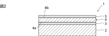
- FIG. 2 is a schematic cross-sectional view of a piezoelectric thin film element according to a second embodiment of the present invention.
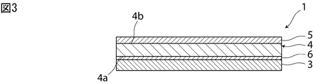
- FIG. 3 is a schematic cross-sectional view of a piezoelectric thin film element according to a third embodiment of the present invention.
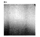
- 4 is a laser microscope image of the surface of the piezoelectric thin film formed in Example 1.
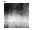
- FIG. FIG. 5 is a laser microscope image of the surface of the piezoelectric thin film formed in Example 2.
- FIG. 6 is a laser microscope image of the surface of the piezoelectric thin film formed in Comparative Example 1.
- FIG. 1 is a schematic cross-sectional view of a piezoelectric thin film element 1 according to a first embodiment of the present invention.
- the piezoelectric thin film element 1 according to the present embodiment will be described with reference to FIG.
- the piezoelectric thin film element 1 has a piezoelectric thin film 4.
- the piezoelectric thin film 4 contains an alkali niobic acid compound.
- the piezoelectric thin film 4 is preferably made of a material mainly composed of an alkali niobic acid compound. More preferably, the alkali niobate compound is an alkali niobate compound having a perovskite structure.
- the alkali niobate compound is preferably a potassium sodium niobate compound containing potassium, sodium and niobium.
- Examples of the potassium sodium niobate compound include compounds represented by the following general formula (1).
- A is at least one element selected from the group consisting of Li, Ag, Ca, Sr, Bi, and Gd.
- B is at least one element selected from the group consisting of Ta, Zr, Ti, Al, Sc and Hf.
- a, b, and c are numbers satisfying the conditions of 0 ⁇ a ⁇ 0.9, 0 ⁇ b ⁇ 0.3, 0 ⁇ a + b ⁇ 0.9, and 0 ⁇ c ⁇ 0.3.
- the thickness of the piezoelectric thin film 4 is usually about 1 ⁇ m to 3 ⁇ m, and preferably about 2 ⁇ m to 3 ⁇ m.
- the first electrode 3 is provided on the first surface 4 a of the piezoelectric thin film 4. Specifically, the first electrode 3 is provided so as to be in contact with the first surface 4 a of the piezoelectric thin film 4.
- the first electrode 3 is a lower electrode.
- the first electrode 3 also serves as a support layer that increases the rigidity of the piezoelectric thin film element 1.
- the first electrode 3 can be formed, for example, by cutting and polishing an ingot, or can be formed by a film forming method such as a sputtering method or a vapor deposition method.
- the first electrode 3 is made of silicon. Specifically, the silicon constituting the first electrode 3 is low resistance silicon. Low-resistance silicon is obtained by doping silicon with arsenic, phosphorus, or the like and having an electric resistance lower than that of pure silicon. The resistivity of the low-resistance silicon constituting the first electrode 3 is preferably 10 ⁇ 3 ⁇ cm or less.
- the surface layer by the side of the piezoelectric thin film 4 should just be comprised with the silicon
- the thickness of the first electrode 3 is usually about 1 ⁇ m to 800 ⁇ m, and is preferably 5 ⁇ m or more in consideration of the role as a support layer.
- a second electrode 5 is provided on the second surface 4 b of the piezoelectric thin film 4. Specifically, the second electrode 5 is provided so as to contact the second surface 4 b of the piezoelectric thin film 4.
- the second electrode 5 is an upper electrode.
- the second electrode 5 can be formed by a film forming method such as a sputtering method or a vapor deposition method.
- the second electrode 5 is made of a metal such as low resistance silicon, Pt, Au, Ag, Ru, Ir, Cu, Ti, Al, an alloy mainly containing at least one of these metals.
- the thickness of the second electrode 5 is usually about 0.05 ⁇ m to 0.3 ⁇ m, and preferably about 0.1 ⁇ m to 0.2 ⁇ m.
- a piezoelectric thin film made of potassium sodium niobate is formed on a Pt layer constituting an electrode made of Pt
- a piezoelectric film is produced when the piezoelectric thin film element is manufactured or when a temperature change occurs in the piezoelectric thin film element. In some cases, cracks are easily formed in the thin film.
- the first electrode 3 made of silicon is provided on the first main surface 4 a of the piezoelectric thin film 4. For this reason, cracks are unlikely to occur in the piezoelectric thin film 4. Although details of the reason why cracks are less likely to occur in the piezoelectric thin film 4 are not clear, such as differences in thermal expansion coefficient and lattice mismatch between the first electrode 3 made of silicon and the piezoelectric thin film 4 containing an alkali niobate compound. It is considered that the stress applied to the piezoelectric thin film 4 is relaxed due to a plurality of factors.
- the piezoelectric thin film element 1 can be manufactured as follows, for example. First, the first electrode 3 made of silicon is formed by a film forming method such as a sputtering method or an evaporation method. Next, the piezoelectric thin film 4 made of a potassium sodium niobate compound is formed on the first electrode 3 by a film forming method such as sputtering or vapor deposition. For example, when the potassium sodium niobate compound constituting the piezoelectric thin film 4 is a compound represented by the general formula (1), the piezoelectric thin film 4 is formed by, for example, a high frequency sputtering method.
- the second electrode 5 is formed on the piezoelectric thin film 4 by a film forming method such as sputtering or vapor deposition. Before or after the second electrode 5 is formed, the piezoelectric thin film 4 may be annealed by a rapid thermal processing apparatus (RTA apparatus: Rapid Thermal Annealing apparatus) or the like. The piezoelectric thin film element 1 is obtained as described above.
- RTA apparatus Rapid Thermal Annealing apparatus
- FIG. 2 is a schematic cross-sectional view of a piezoelectric thin film element 1 according to the second embodiment of the present invention.
- the piezoelectric thin film element 1 has a support layer 2.
- the first electrode 3 is provided on the support layer 2. Since the piezoelectric thin film element 1 has the support layer 2, the rigidity of the piezoelectric thin film element 1 is enhanced.
- the material which comprises the support layer 2 is not specifically limited.
- the material constituting the support layer 2 examples include silicon, low-temperature fired ceramics, insulating ceramics such as Al 2 O 3 , piezoelectric single-pieces such as LiTaO 3 , LiNbO 3 , and quartz, semiconductors such as SiC, GaAs, and GaN, Glass etc. are mentioned.
- the support layer 2 is made of silicon, the support layer 2 is preferably made of silicon doped with arsenic or phosphorus and having a resistivity of 10 ⁇ 2 ⁇ cm or less.
- arsenic or phosphorus is doped to a depth of about 0.01 to 0.1 ⁇ m from one main surface of a silicon substrate or the like, and the surface layer with a reduced resistance is used as the first electrode. 3 and other portions may be the support layer 2.
- the thickness of the support layer 2 is usually about 50 ⁇ m to 800 ⁇ m.
- FIG. 3 is a schematic cross-sectional view of a piezoelectric thin film element 1 according to a third embodiment of the present invention.
- a seed layer 6 is provided between the piezoelectric thin film 4 and the first electrode 3.
- the crystal orientation of the alkali niobate compound constituting the piezoelectric thin film 4 can be enhanced. For this reason, it can suppress more effectively that a crack is formed in the piezoelectric thin film 4.
- the seed layer 6 is made of a LaNiO 3, LaScO 3, LaGaO 3 , KNbO 3, NaNbO 3, perovskite oxide such as SrRuO 3, ZnO, TiO 2, oxides such as CeO 2, AlN, nitrides such as ZrN It is preferably composed of at least one selected from the group, and more preferably composed of LaNiO 3 . Note that a film formed by forming the same material as the piezoelectric thin film 4 at a temperature of about 300 ° C. may be used as the seed layer 6.
- the thickness of the seed layer 6 is preferably 10 nm or more, and preferably 200 nm or less.
- Example 1 A silicon substrate having a thickness of 500 ⁇ m is prepared, and arsenic is doped to a depth of about 0.01 to 0.1 ⁇ m from one main surface of the silicon substrate, so that the surface layer whose resistance has been reduced is the first electrode. 3 and a low resistance silicon substrate in which the other part constitutes the support layer 2 was formed.
- the temperature of the first electrode 3 is 600 ° C.
- the sputtering pressure is 0.1.
- FIG. 4 shows a laser microscope image (within a field of view of 125 ⁇ m on one side) of the surface of the piezoelectric thin film 4 formed in Example 1.
- Example 2 A silicon substrate having a thickness of 500 ⁇ m is prepared, and arsenic is doped to a depth of about 0.01 to 0.1 ⁇ m from one main surface of the silicon substrate, so that the surface layer whose resistance has been reduced is the first electrode. 3 and a low resistance silicon substrate in which the other part constitutes the support layer 2 was formed.
- the temperature of the first electrode 3 is 300 ° C.
- the sputtering pressure is 0.1.
- a seed layer 6 of LaNiO 3 having a thickness of 30 nm was formed by sputtering using a target having a composition of LaNiO 3 under the condition of 27 Pa.
- the temperature of the first electrode 3 is 600 ° C.
- the sputtering pressure is 0.3 Pa.
- a piezoelectric thin film 4 having a thickness of 2 ⁇ m and made of a potassium sodium niobate compound was formed by sputtering using a target having a composition of (K 0.5 , Na 0.5 ) NbO 3 under the conditions.
- FIG. 5 shows a laser microscope image (within a field of view of 125 ⁇ m on one side) of the surface of the piezoelectric thin film 4 formed in Example 2.
- a silicon substrate having a thickness of 300 ⁇ m and a thermal oxide film having a thickness of 700 nm formed on the surface was prepared.
- An adhesion layer made of TiO 2 having a thickness of 20 nm was formed on the silicon substrate by sputtering.
- a first electrode made of Pt and having a thickness of 100 nm was formed on the adhesion layer by sputtering under the conditions that the temperature of the silicon substrate was 430 ° C., the Ar atmosphere, and the sputtering pressure was 0.4 Pa.
- the temperature of the silicon substrate is 300 ° C.
- the sputtering pressure is 0.27 Pa.
- a seed layer having a thickness of 30 nm and made of LaNiO 3 was formed by a sputtering method using a target having a composition of LaNiO 3 .
- the temperature of the silicon substrate is 600 ° C.
- the sputtering pressure is 0.3 Pa
- a piezoelectric thin film having a thickness of 2 ⁇ m and made of a potassium sodium niobate compound was formed by sputtering using a target having a composition of K 0.5 , Na 0.5 ) NbO 3 .
- FIG. 6 shows a laser microscope image (within a field of view of 125 ⁇ m on one side) of the surface of the piezoelectric thin film formed in Comparative Example 1.
- a silicon substrate having a thickness of 300 ⁇ m and a thermal oxide film having a thickness of 700 nm formed on the surface was prepared.
- An adhesion layer made of TiO 2 having a thickness of 20 nm was formed on the silicon substrate by sputtering.
- a first electrode made of Pt and having a thickness of 100 nm was formed on the adhesion layer by sputtering under the conditions that the temperature of the silicon substrate was 430 ° C., the Ar atmosphere, and the sputtering pressure was 0.4 Pa.
- the temperature of the silicon substrate is 600 ° C.
- the partial pressure of O 2 / (Ar partial pressure + O 2 partial pressure) 0.1
- the sputtering pressure is 0.3 Pa.
- a piezoelectric thin film made of a potassium sodium niobate compound and having a thickness of 2 ⁇ m was formed by sputtering using a target having a composition of (K 0.5 , Na 0.5 ) NbO 3 .
Landscapes
- Engineering & Computer Science (AREA)
- Manufacturing & Machinery (AREA)
- Chemical & Material Sciences (AREA)
- Materials Engineering (AREA)
- Ceramic Engineering (AREA)
- Physical Vapour Deposition (AREA)
Description
本発明は、圧電薄膜素子及びその製造方法に関する。
従来、圧電薄膜と電極とが設けられた圧電薄膜素子が知られている。このような圧電薄膜素子は、角速度センサや加速度センサなどの各種センサ、アクチュエータ、高周波フィルタなどとして用いられる。
例えば、特許文献1には、Ptからなる電極の上に、ニオブ酸カリウムナトリウム(一般式:(KxNa1-x)NbO3(0<x<1))からなる圧電薄膜が設けられた、圧電薄膜素子が開示されている。
このような圧電薄膜素子の製造工程においては、一般に、Ptからなる電極を構成するPt層の上にニオブ酸カリウムナトリウムからなる圧電薄膜を形成する。しかしながら、Pt層の上にニオブ酸カリウムナトリウムからなる圧電薄膜を形成すると、圧電薄膜素子の製造時や、圧電薄膜素子に温度変化が生じた際に、圧電薄膜にクラックが形成されやすくなる場合がある。
本発明は、圧電薄膜にクラックが形成されにくい圧電薄膜素子及びその製造方法を提供することを主な目的とする。
本発明の圧電薄膜素子は、圧電薄膜と、第1の電極と、第2の電極とを備える。圧電薄膜は、アルカリニオブ酸系化合物を含む。第1の電極は、圧電薄膜の一方側主面に設けられている。第2の電極は、圧電薄膜の他方側主面に設けられている。第1の電極は、シリコンからなる。
本発明の圧電薄膜素子のある特定の局面では、圧電薄膜と、第1の電極との間には、シード層が設けられている。
本発明の圧電薄膜素子の他の特定の局面では、シード層が、LaNiO3,LaScO3,LaGaO3,KNbO3,NaNbO3,SrRuO3などのペロブスカイト型酸化物、ZnO,TiO2,CeO2などの酸化物、AlN,ZrNなどの窒化物からなる群から選択された少なくとも1種により構成されている。
本発明の圧電薄膜素子の製造方法では、シリコンからなる電極の上に、アルカリニオブ酸系化合物を含む圧電薄膜を形成する。
本発明によれば、圧電薄膜にクラックが形成されにくい圧電薄膜素子及びその製造方法を提供することができる。
以下、本発明を実施した好ましい形態の一例について説明する。但し、下記の実施形態は、単なる例示である。本発明は、下記の実施形態に何ら限定されない。
また、実施形態等において参照する各図面において、実質的に同一の機能を有する部材は同一の符号で参照することとする。また、実施形態等において参照する図面は、模式的に記載されたものであり、図面に描画された物体の寸法の比率などは、現実の物体の寸法の比率などとは異なる場合がある。図面相互間においても、物体の寸法比率等が異なる場合がある。具体的な物体の寸法比率等は、以下の説明を参酌して判断されるべきである。
図1は、本発明の第1の実施形態に係る圧電薄膜素子1の略図的断面図である。以下、図1を参照しながら、本実施形態に係る圧電薄膜素子1について説明する。
図1に示されるように、圧電薄膜素子1は、圧電薄膜4を有する。圧電薄膜4は、アルカリニオブ酸系化合物を含む。圧電薄膜4は、アルカリニオブ酸系化合物を主とする材料からなることが好ましい。アルカリニオブ酸系化合物は、ペロブスカイト型構造を有するアルカリニオブ酸系化合物であることがより好ましい。
また、アルカリニオブ酸系化合物は、カリウム、ナトリウム及びニオブを含むニオブ酸カリウムナトリウム系化合物であることが好ましい。ニオブ酸カリウムナトリウム系化合物としては、例えば下記一般式(1)で表される化合物が挙げられる。
(K1-a-b/2Naa-b/2Ab)(Nb1-cBc)O3 (1)
一般式(1)において、Aは、Li,Ag,Ca,Sr,Bi及びGdからなる群から選択された少なくとも1種の元素である。Bは、Ta,Zr,Ti,Al,Sc及びHfからなる群から選択された少なくとも1種の元素である。a、b及びcは、0<a≦0.9、0≦b≦0.3、0≦a+b≦0.9、0≦c≦0.3の条件を満たす数である。
一般式(1)において、Aは、Li,Ag,Ca,Sr,Bi及びGdからなる群から選択された少なくとも1種の元素である。Bは、Ta,Zr,Ti,Al,Sc及びHfからなる群から選択された少なくとも1種の元素である。a、b及びcは、0<a≦0.9、0≦b≦0.3、0≦a+b≦0.9、0≦c≦0.3の条件を満たす数である。
圧電薄膜4の厚みは、通常1μm~3μm程度であり、2μm~3μm程度であることが好ましい。
圧電薄膜4の第1の表面4aには、第1の電極3が設けられている。具体的には、圧電薄膜4の第1の表面4aと当接するように、第1の電極3が設けられている。第1の電極3は下部電極である。第1の電極3は、圧電薄膜素子1の剛性を高める支持層としての役割も有する。第1の電極3は、例えばインゴットを切削及び研磨することで形成することができるし、スパッタリング法や蒸着法などの成膜方法によっても形成することができる。
第1の電極3はシリコンからなる。具体的には、第1の電極3を構成するシリコンは、低抵抗シリコンである。低抵抗シリコンは、ヒ素やリンなどがシリコンにドープされ、ピュアなシリコンよりも電気抵抗が低くなったものである。第1の電極3を構成する低抵抗シリコンの抵抗率は、10-3Ωcm以下であることが好ましい。第1の電極3においては、圧電薄膜4側の表層がシリコンにより構成されていればよく、他の部分は、他の材料により構成されていてもよい。他の材料としては、例えば、SiO2やSiNなどのシリコン系化合物、Pt,Au,Ag,Ru,Ir,Cu,Ti,Alなどの金属、これらの金属のうち少なくとも1種を主成分とする合金などが挙げられる。
第1の電極3の厚みは、通常1μm~800μm程度であり、支持層としての役割を考慮すると5μm以上であることが好ましい。
圧電薄膜4の第2の表面4bには、第2の電極5が設けられている。具体的には、圧電薄膜4の第2の表面4bと当接するように、第2の電極5が設けられている。第2の電極5は上部電極である。第2の電極5は、例えばスパッタリング法や蒸着法などの成膜方法により形成することができる。
第2の電極5は、低抵抗シリコン、Pt,Au,Ag、Ru,Ir、Cu、Ti、Alなどの金属、これらの金属のうち少なくとも1種を主成分とする合金などからなる。
第2の電極5の厚みは、通常0.05μm~0.3μm程度であり、0.1μm~0.2μm程度であることが好ましい。
上述の通り、例えばPtからなる電極を構成するPt層の上にニオブ酸カリウムナトリウムからなる圧電薄膜を形成すると、圧電薄膜素子の製造時や、圧電薄膜素子に温度変化が生じた際に、圧電薄膜にクラックが形成されやすくなる場合がある。
これに対して、圧電薄膜素子1では、圧電薄膜4の第1の主面4aに、シリコンからなる第1の電極3が設けられている。このため、圧電薄膜4にクラックが生じにくい。圧電薄膜4にクラックが生じにくくなる理由の詳細は、明らかではないが、シリコンからなる第1の電極3とアルカリニオブ酸系化合物を含む圧電薄膜4との熱膨張係数の差や格子ミスマッチなどの複数の要因により、圧電薄膜4にかかる応力が緩和されていることによるものと考えられる。
圧電薄膜素子1は、例えば、次のようにして製造することができる。まず、スパッタリング法、蒸着法などの成膜方法などにより、シリコンからなる第1の電極3を形成する。次に、第1の電極3の上に、スパッタリング法、蒸着法などの成膜方法などにより、ニオブ酸カリウムナトリウム系化合物からなる圧電薄膜4を形成する。例えば、圧電薄膜4を構成するニオブ酸カリウムナトリウム系化合物が、上記一般式(1)で表される化合物である場合、圧電薄膜4は、例えば高周波スパッタリング法により形成される。このとき、圧電薄膜4は、第1の電極3の温度が400℃~700℃程度、O2の分圧/(Arの分圧+O2の分圧)=0.05~0.5、スパッタ圧力が0.3Pa~1.5Pa程度となる条件で、高周波スパッタリング法により形成されることが好ましい。次に、圧電薄膜4の上に、スパッタリング法や蒸着法などの成膜方法により、第2の電極5を形成する。第2の電極5を形成する前または形成した後に、高速熱処理装置(RTA装置:Rapid Thermal Annealing装置)などによって圧電薄膜4をアニール処理してもよい。以上のようにして、圧電薄膜素子1が得られる。
(第2の実施形態)
図2は、本発明の第2の実施形態に係る圧電薄膜素子1の略図的断面図である。図2に示されるように、本実施形態において、圧電薄膜素子1は、支持層2を有する。具体的には、圧電薄膜素子1において、第1の電極3は、支持層2の上に設けられている。圧電薄膜素子1が支持層2を有することにより、圧電薄膜素子1の剛性が高められている。支持層2を構成する材料は特に限定されない。支持層2を構成する材料としては、例えばシリコン、低温焼成セラミックス、Al2O3などの絶縁性セラミックス、LiTaO3,LiNbO3,水晶などの圧電単結品、SiC,GaAs,GaNなどの半導体、ガラスなどが挙げられる。支持層2がシリコンからなる場合、支持層2は、ヒ素やリンなどがドープされていて、抵抗率が10-2Ωcm以下であるシリコンにより構成されていることが好ましい。
図2は、本発明の第2の実施形態に係る圧電薄膜素子1の略図的断面図である。図2に示されるように、本実施形態において、圧電薄膜素子1は、支持層2を有する。具体的には、圧電薄膜素子1において、第1の電極3は、支持層2の上に設けられている。圧電薄膜素子1が支持層2を有することにより、圧電薄膜素子1の剛性が高められている。支持層2を構成する材料は特に限定されない。支持層2を構成する材料としては、例えばシリコン、低温焼成セラミックス、Al2O3などの絶縁性セラミックス、LiTaO3,LiNbO3,水晶などの圧電単結品、SiC,GaAs,GaNなどの半導体、ガラスなどが挙げられる。支持層2がシリコンからなる場合、支持層2は、ヒ素やリンなどがドープされていて、抵抗率が10-2Ωcm以下であるシリコンにより構成されていることが好ましい。
本実施形態においては、例えば、シリコン基板などの一方側主面の上から、0.01~0.1μm程度の深さまでヒ素やリンなどをドープし、低抵抗化された表層を第1の電極3とし、他の部分を支持層2としてもよい。支持層2の厚みは、通常50μm~800μm程度である。
(第3の実施形態)
図3は、本発明の第3の実施形態に係る圧電薄膜素子1の略図的断面図である。図3に示されるように、本実施形態においては、圧電薄膜4と第1の電極3との間にシード層6が設けられている。圧電薄膜4と第1の電極3との間に、シード層6が設けられていることにより、圧電薄膜4を構成するアルカリニオブ酸系化合物の結晶の配向性を高めることができる。このため、圧電薄膜4にクラックが形成されることをより効果的に抑制し得る。シード層6は、LaNiO3,LaScO3,LaGaO3,KNbO3,NaNbO3,SrRuO3などのペロブスカイト型酸化物、ZnO,TiO2,CeO2などの酸化物、AlN,ZrNなどの窒化物からなる群から選択された少なくとも1種により構成されることが好ましく、LaNiO3により構成されることがより好ましい。なお、圧電薄膜4と同じ材料を300℃程度の温度で成膜して作製された膜をシード層6としてもよい。
図3は、本発明の第3の実施形態に係る圧電薄膜素子1の略図的断面図である。図3に示されるように、本実施形態においては、圧電薄膜4と第1の電極3との間にシード層6が設けられている。圧電薄膜4と第1の電極3との間に、シード層6が設けられていることにより、圧電薄膜4を構成するアルカリニオブ酸系化合物の結晶の配向性を高めることができる。このため、圧電薄膜4にクラックが形成されることをより効果的に抑制し得る。シード層6は、LaNiO3,LaScO3,LaGaO3,KNbO3,NaNbO3,SrRuO3などのペロブスカイト型酸化物、ZnO,TiO2,CeO2などの酸化物、AlN,ZrNなどの窒化物からなる群から選択された少なくとも1種により構成されることが好ましく、LaNiO3により構成されることがより好ましい。なお、圧電薄膜4と同じ材料を300℃程度の温度で成膜して作製された膜をシード層6としてもよい。
シード層6の厚みが薄すぎると、アルカリニオブ酸系化合物の結晶の配向性を高める効果が小さくなる場合がある。また、シード層6の厚みが厚すぎると、圧電薄膜4に電圧が印加されにくくなったり、厚みのばらつきが生じてシード層6の表面の平坦性が悪くなる場合がある。よって、シード層6の厚みは、10nm以上であることが好ましく、200nm以下であることが好ましい。
以下、本発明について、具体的な実施例に基づいて、さらに詳細に説明する。本発明は、以下の実施例に何ら限定されるものではなく、その要旨を変更しない範囲において適宜変更して実施することが可能である。
(実施例1)
厚みが500μmであるシリコン基板を用意し、シリコン基板の一方側主面の上から0.01~0.1μm程度の深さまでヒ素をドープすることによって、低抵抗化された表層が第1の電極3を構成し、他の部分が支持層2を構成する、低抵抗シリコン基板を形成した。次に、第1の電極3の上に、第1の電極3の温度が600℃、O2の分圧/(Arの分圧+O2の分圧)=0.1、スパッタ圧力が0.3Paである条件で、組成が(K0.5,Na0.5)NbO3であるターゲットを用いたスパッタリング法により、厚みが2μmであり、ニオブ酸カリウムナトリウム系化合物からなる圧電薄膜4を形成した。
厚みが500μmであるシリコン基板を用意し、シリコン基板の一方側主面の上から0.01~0.1μm程度の深さまでヒ素をドープすることによって、低抵抗化された表層が第1の電極3を構成し、他の部分が支持層2を構成する、低抵抗シリコン基板を形成した。次に、第1の電極3の上に、第1の電極3の温度が600℃、O2の分圧/(Arの分圧+O2の分圧)=0.1、スパッタ圧力が0.3Paである条件で、組成が(K0.5,Na0.5)NbO3であるターゲットを用いたスパッタリング法により、厚みが2μmであり、ニオブ酸カリウムナトリウム系化合物からなる圧電薄膜4を形成した。
実施例1で形成した圧電薄膜4の表面のレーザー顕微鏡像(一辺が125μmの視野内)を図4に示す。
(実施例2)
厚みが500μmであるシリコン基板を用意し、シリコン基板の一方側主面の上から0.01~0.1μm程度の深さまでヒ素をドープすることによって、低抵抗化された表層が第1の電極3を構成し、他の部分が支持層2を構成する、低抵抗シリコン基板を形成した。次に、第1の電極3の上に、第1の電極3の温度が300℃、O2の分圧/(Arの分圧+O2の分圧)=0.9、スパッタ圧力が0.27Paである条件で、組成がLaNiO3であるターゲットを用いたスパッタリング法により、厚みが30nmであり、LaNiO3からなるシード層6を形成した。そして、シード層6の上に、第1の電極3の温度が600℃、O2の分圧/(Arの分圧+O2の分圧)=0.1、スパッタ圧力が0.3Paである条件で、(K0.5,Na0.5)NbO3の組成のターゲットを用いたスパッタリング法により、厚みが2μmであり、ニオブ酸カリウムナトリウム系化合物からなる圧電薄膜4を形成した。
厚みが500μmであるシリコン基板を用意し、シリコン基板の一方側主面の上から0.01~0.1μm程度の深さまでヒ素をドープすることによって、低抵抗化された表層が第1の電極3を構成し、他の部分が支持層2を構成する、低抵抗シリコン基板を形成した。次に、第1の電極3の上に、第1の電極3の温度が300℃、O2の分圧/(Arの分圧+O2の分圧)=0.9、スパッタ圧力が0.27Paである条件で、組成がLaNiO3であるターゲットを用いたスパッタリング法により、厚みが30nmであり、LaNiO3からなるシード層6を形成した。そして、シード層6の上に、第1の電極3の温度が600℃、O2の分圧/(Arの分圧+O2の分圧)=0.1、スパッタ圧力が0.3Paである条件で、(K0.5,Na0.5)NbO3の組成のターゲットを用いたスパッタリング法により、厚みが2μmであり、ニオブ酸カリウムナトリウム系化合物からなる圧電薄膜4を形成した。
実施例2で形成した圧電薄膜4の表面のレーザー顕微鏡像(一辺が125μmの視野内)を図5に示す。
(比較例1)
支持層として、厚みが300μmであり、厚みが700nmの熱酸化膜が表面に形成されている、シリコン基板を用意した。シリコン基板の上に、スパッタリング法により、厚みが20nmであり、TiO2からなる密着層を形成した。密着層の上に、スパッタリング法により、シリコン基板の温度が430℃、Ar雰囲気、スパッタ圧力が0.4Paである条件で、厚みが100nmであり、Ptからなる第1の電極を形成した。次に、第1の電極の上に、シリコン基板の温度が300℃、O2の分圧/(Arの分圧+O2の分圧)=0.9、スパッタ圧力が0.27Paである条件で、組成がLaNiO3であるターゲットを用いたスパッタリング法により、厚みが30nmであり、LaNiO3からなるシード層を形成した。そして、シード層の上に、シリコン基板の温度が600℃、O2の分圧/(Arの分圧+O2の分圧)=0.1、スパッタ圧力が0.3Paである条件で、(K0.5,Na0.5)NbO3の組成のターゲットを用いたスパッタリング法により、厚みが2μmであり、ニオブ酸カリウムナトリウム系化合物からなる圧電薄膜を形成した。
支持層として、厚みが300μmであり、厚みが700nmの熱酸化膜が表面に形成されている、シリコン基板を用意した。シリコン基板の上に、スパッタリング法により、厚みが20nmであり、TiO2からなる密着層を形成した。密着層の上に、スパッタリング法により、シリコン基板の温度が430℃、Ar雰囲気、スパッタ圧力が0.4Paである条件で、厚みが100nmであり、Ptからなる第1の電極を形成した。次に、第1の電極の上に、シリコン基板の温度が300℃、O2の分圧/(Arの分圧+O2の分圧)=0.9、スパッタ圧力が0.27Paである条件で、組成がLaNiO3であるターゲットを用いたスパッタリング法により、厚みが30nmであり、LaNiO3からなるシード層を形成した。そして、シード層の上に、シリコン基板の温度が600℃、O2の分圧/(Arの分圧+O2の分圧)=0.1、スパッタ圧力が0.3Paである条件で、(K0.5,Na0.5)NbO3の組成のターゲットを用いたスパッタリング法により、厚みが2μmであり、ニオブ酸カリウムナトリウム系化合物からなる圧電薄膜を形成した。
比較例1で形成した圧電薄膜の表面のレーザー顕微鏡像(一辺が125μmの視野内)を図6に示す。
(比較例2)
支持層として、厚みが300μmであり、厚みが700nmの熱酸化膜が表面に形成されている、シリコン基板を用意した。シリコン基板の上に、スパッタリング法により、厚みが20nmであり、TiO2からなる密着層を形成した。密着層の上に、スパッタリング法により、シリコン基板の温度が430℃、Ar雰囲気、スパッタ圧力が0.4Paである条件で、厚みが100nmであり、Ptからなる第1の電極を形成した。次に、第1の電極の上に、シリコン基板の温度が600℃、O2の分圧/(Arの分圧+O2の分圧)=0.1、スパッタ圧力が0.3Paである条件で、(K0.5,Na0.5)NbO3の組成のターゲットを用いたスパッタリング法により、厚みが2μmであり、ニオブ酸カリウムナトリウム系化合物からなる圧電薄膜を形成した。
支持層として、厚みが300μmであり、厚みが700nmの熱酸化膜が表面に形成されている、シリコン基板を用意した。シリコン基板の上に、スパッタリング法により、厚みが20nmであり、TiO2からなる密着層を形成した。密着層の上に、スパッタリング法により、シリコン基板の温度が430℃、Ar雰囲気、スパッタ圧力が0.4Paである条件で、厚みが100nmであり、Ptからなる第1の電極を形成した。次に、第1の電極の上に、シリコン基板の温度が600℃、O2の分圧/(Arの分圧+O2の分圧)=0.1、スパッタ圧力が0.3Paである条件で、(K0.5,Na0.5)NbO3の組成のターゲットを用いたスパッタリング法により、厚みが2μmであり、ニオブ酸カリウムナトリウム系化合物からなる圧電薄膜を形成した。
比較例2で得られた圧電薄膜の表面をレーザー顕微鏡で観察したところ、圧電薄膜の表面構造が粗く、上部電極を形成するには適しておらず、圧電薄膜素子に求められる機能を実現することが困難であることが分かった。
1…圧電薄膜素子
2…支持層
3…第1の電極
4…圧電薄膜
4a…圧電薄膜の第1の表面
4b…圧電薄膜の第2の表面
5…第2の電極
6…シード層
2…支持層
3…第1の電極
4…圧電薄膜
4a…圧電薄膜の第1の表面
4b…圧電薄膜の第2の表面
5…第2の電極
6…シード層
Claims (4)
- アルカリニオブ酸系化合物を含む圧電薄膜と、
前記圧電薄膜の一方側主面に設けられた第1の電極と、
前記圧電薄膜の他方側主面に設けられた第2の電極と、
を備え、
前記第1の電極が、シリコンからなる、圧電薄膜素子。 - 前記圧電薄膜と、前記第1の電極との間には、シード層が設けられている、請求項1に記載の圧電薄膜素子。
- 前記シード層が、LaNiO3,LaScO3,LaGaO3,KNbO3,NaNbO3,SrRuO3などのペロブスカイト型酸化物、ZnO,TiO2,CeO2などの酸化物、AlN,ZrNなどの窒化物からなる群から選択された少なくとも1種により構成されている、請求項1または2に記載の圧電薄膜素子。
- シリコンからなる電極の上に、アルカリニオブ酸系化合物を含む圧電薄膜を形成する、圧電薄膜素子の製造方法。
Priority Applications (1)
| Application Number | Priority Date | Filing Date | Title |
|---|---|---|---|
| JP2014523652A JPWO2014007015A1 (ja) | 2012-07-02 | 2013-06-04 | 圧電薄膜素子及びその製造方法 |
Applications Claiming Priority (2)
| Application Number | Priority Date | Filing Date | Title |
|---|---|---|---|
| JP2012-148123 | 2012-07-02 | ||
| JP2012148123 | 2012-07-02 |
Publications (1)
| Publication Number | Publication Date |
|---|---|
| WO2014007015A1 true WO2014007015A1 (ja) | 2014-01-09 |
Family
ID=49881775
Family Applications (1)
| Application Number | Title | Priority Date | Filing Date |
|---|---|---|---|
| PCT/JP2013/065462 Ceased WO2014007015A1 (ja) | 2012-07-02 | 2013-06-04 | 圧電薄膜素子及びその製造方法 |
Country Status (2)
| Country | Link |
|---|---|
| JP (1) | JPWO2014007015A1 (ja) |
| WO (1) | WO2014007015A1 (ja) |
Cited By (5)
| Publication number | Priority date | Publication date | Assignee | Title |
|---|---|---|---|---|
| CN108140723A (zh) * | 2015-12-02 | 2018-06-08 | 株式会社村田制作所 | 压电元件、压电传声器、压电谐振子以及压电元件的制造方法 |
| JPWO2020250591A1 (ja) * | 2019-06-12 | 2020-12-17 | ||
| JPWO2020250632A1 (ja) * | 2019-06-12 | 2020-12-17 | ||
| WO2023223815A1 (ja) * | 2022-05-16 | 2023-11-23 | Agc株式会社 | 圧電積層体、圧電素子、および圧電積層体の製造方法 |
| US12404167B2 (en) * | 2021-09-28 | 2025-09-02 | Skyworks Global Pte. Ltd. | Piezoelectric MEMS device with thermal compensation from different material thicknesses |
Citations (3)
| Publication number | Priority date | Publication date | Assignee | Title |
|---|---|---|---|---|
| JP2009117785A (ja) * | 2007-10-15 | 2009-05-28 | Hitachi Cable Ltd | 圧電薄膜付き基板 |
| WO2011132532A1 (ja) * | 2010-04-23 | 2011-10-27 | 株式会社村田製作所 | 圧電アクチュエータおよび圧電アクチュエータの製造方法 |
| WO2012020638A1 (ja) * | 2010-08-12 | 2012-02-16 | 株式会社村田製作所 | 圧電薄膜素子の製造方法、圧電薄膜素子及び圧電薄膜素子用部材 |
Family Cites Families (3)
| Publication number | Priority date | Publication date | Assignee | Title |
|---|---|---|---|---|
| JP4983586B2 (ja) * | 2007-12-19 | 2012-07-25 | 株式会社デンソー | 弾性表面波角速度センサ |
| US8087153B2 (en) * | 2008-06-24 | 2012-01-03 | Canon Kabushiki Kaisha | Manufacturing method of an electromechanical transducer |
| JP2010118730A (ja) * | 2008-11-11 | 2010-05-27 | Toshiba Corp | 圧電デバイス及びその製造方法 |
-
2013
- 2013-06-04 JP JP2014523652A patent/JPWO2014007015A1/ja active Pending
- 2013-06-04 WO PCT/JP2013/065462 patent/WO2014007015A1/ja not_active Ceased
Patent Citations (3)
| Publication number | Priority date | Publication date | Assignee | Title |
|---|---|---|---|---|
| JP2009117785A (ja) * | 2007-10-15 | 2009-05-28 | Hitachi Cable Ltd | 圧電薄膜付き基板 |
| WO2011132532A1 (ja) * | 2010-04-23 | 2011-10-27 | 株式会社村田製作所 | 圧電アクチュエータおよび圧電アクチュエータの製造方法 |
| WO2012020638A1 (ja) * | 2010-08-12 | 2012-02-16 | 株式会社村田製作所 | 圧電薄膜素子の製造方法、圧電薄膜素子及び圧電薄膜素子用部材 |
Cited By (9)
| Publication number | Priority date | Publication date | Assignee | Title |
|---|---|---|---|---|
| CN108140723A (zh) * | 2015-12-02 | 2018-06-08 | 株式会社村田制作所 | 压电元件、压电传声器、压电谐振子以及压电元件的制造方法 |
| JPWO2020250591A1 (ja) * | 2019-06-12 | 2020-12-17 | ||
| JPWO2020250632A1 (ja) * | 2019-06-12 | 2020-12-17 | ||
| JP7167338B2 (ja) | 2019-06-12 | 2022-11-08 | 富士フイルム株式会社 | 圧電素子及び圧電素子の作製方法 |
| JP7167337B2 (ja) | 2019-06-12 | 2022-11-08 | 富士フイルム株式会社 | 圧電素子及び圧電素子の作製方法 |
| US11985899B2 (en) | 2019-06-12 | 2024-05-14 | Fujifilm Corporation | Piezoelectric element |
| US12414473B2 (en) | 2019-06-12 | 2025-09-09 | Fujifilm Corporation | Piezoelectric element |
| US12404167B2 (en) * | 2021-09-28 | 2025-09-02 | Skyworks Global Pte. Ltd. | Piezoelectric MEMS device with thermal compensation from different material thicknesses |
| WO2023223815A1 (ja) * | 2022-05-16 | 2023-11-23 | Agc株式会社 | 圧電積層体、圧電素子、および圧電積層体の製造方法 |
Also Published As
| Publication number | Publication date |
|---|---|
| JPWO2014007015A1 (ja) | 2016-06-02 |
Similar Documents
| Publication | Publication Date | Title |
|---|---|---|
| JP5692329B2 (ja) | 圧電薄膜素子 | |
| JP5801364B2 (ja) | 圧電薄膜付き基板及び圧電素子 | |
| JP5471612B2 (ja) | 圧電性薄膜素子の製造方法及び圧電薄膜デバイスの製造方法 | |
| JP5024399B2 (ja) | 圧電薄膜素子、圧電薄膜デバイス及び圧電薄膜素子の製造方法 | |
| US11081637B2 (en) | Laminate structure, piezoelectric element, and method of manufacturing piezoelectric element | |
| CN104078560B (zh) | 压电体薄膜层叠基板 | |
| JP2013016776A (ja) | 圧電膜素子の製造方法、及び圧電体デバイスの製造方法 | |
| WO2014007015A1 (ja) | 圧電薄膜素子及びその製造方法 | |
| US10964879B2 (en) | Method of manufacturing a dielectric device | |
| JP6850870B2 (ja) | 圧電体膜、圧電素子、及び、圧電素子の製造方法 | |
| JP2010135669A (ja) | 薄膜圧電体付き基板、薄膜圧電体素子、薄膜圧電体デバイスおよび薄膜圧電体付き基板の製造方法 | |
| JP6426061B2 (ja) | 積層薄膜構造体の製造方法、積層薄膜構造体及びそれを備えた圧電素子 | |
| US20200044138A1 (en) | Device based on alkali metal niobate comprising a barrier layer and manufacturing process | |
| JP7679976B2 (ja) | 圧電薄膜及びその作製方法 | |
| JP5790226B2 (ja) | 圧電薄膜素子の製造方法 | |
| JP6311179B2 (ja) | 強誘電体セラミックス | |
| JP7667051B2 (ja) | 圧電積層体及び圧電素子 | |
| JP5434563B2 (ja) | 圧電体薄膜付き基板の製造方法 | |
| WO2025070424A1 (ja) | Baw共振器、bawデバイス及び電子機器 | |
| WO2011099231A1 (ja) | 圧電薄膜素子、圧電薄膜デバイス及び圧電薄膜素子の製造方法 | |
| JP2019057699A (ja) | 圧電素子、及び、圧電素子の製造方法 | |
| JP2012253243A (ja) | 圧電膜素子、圧電膜素子の製造方法、及び圧電デバイス | |
| JP2015056517A (ja) | 圧電体薄膜積層基板およびその製造方法 |
Legal Events
| Date | Code | Title | Description |
|---|---|---|---|
| 121 | Ep: the epo has been informed by wipo that ep was designated in this application |
Ref document number: 13813821 Country of ref document: EP Kind code of ref document: A1 |
|
| ENP | Entry into the national phase |
Ref document number: 2014523652 Country of ref document: JP Kind code of ref document: A |
|
| NENP | Non-entry into the national phase |
Ref country code: DE |
|
| 122 | Ep: pct application non-entry in european phase |
Ref document number: 13813821 Country of ref document: EP Kind code of ref document: A1 |