WO2014007014A1 - Élément de circuit non réciproque - Google Patents
Élément de circuit non réciproque Download PDFInfo
- Publication number
- WO2014007014A1 WO2014007014A1 PCT/JP2013/065440 JP2013065440W WO2014007014A1 WO 2014007014 A1 WO2014007014 A1 WO 2014007014A1 JP 2013065440 W JP2013065440 W JP 2013065440W WO 2014007014 A1 WO2014007014 A1 WO 2014007014A1
- Authority
- WO
- WIPO (PCT)
- Prior art keywords
- center conductor
- port
- terminal
- conductor
- capacitive element
- Prior art date
Links
Images


Classifications
-
- H—ELECTRICITY
- H01—ELECTRIC ELEMENTS
- H01P—WAVEGUIDES; RESONATORS, LINES, OR OTHER DEVICES OF THE WAVEGUIDE TYPE
- H01P1/00—Auxiliary devices
- H01P1/32—Non-reciprocal transmission devices
- H01P1/38—Circulators
- H01P1/383—Junction circulators, e.g. Y-circulators
-
- H—ELECTRICITY
- H01—ELECTRIC ELEMENTS
- H01P—WAVEGUIDES; RESONATORS, LINES, OR OTHER DEVICES OF THE WAVEGUIDE TYPE
- H01P1/00—Auxiliary devices
- H01P1/32—Non-reciprocal transmission devices
- H01P1/38—Circulators
- H01P1/383—Junction circulators, e.g. Y-circulators
- H01P1/387—Strip line circulators
-
- H—ELECTRICITY
- H01—ELECTRIC ELEMENTS
- H01F—MAGNETS; INDUCTANCES; TRANSFORMERS; SELECTION OF MATERIALS FOR THEIR MAGNETIC PROPERTIES
- H01F7/00—Magnets
- H01F7/02—Permanent magnets [PM]
Definitions
- the present invention relates to non-reciprocal circuit elements, and more particularly to non-reciprocal circuit elements such as isolators and circulators used in the microwave band.
- nonreciprocal circuit elements such as isolators and circulators have a characteristic of transmitting a signal only in a predetermined specific direction and not transmitting in a reverse direction. Utilizing this characteristic, for example, an isolator is used in a transmission circuit unit of a mobile communication device such as a mobile phone.
- the circulator S is mounted between the noise canceller NC and the antenna ANT.
- the circulator S cancels the noise in the reception band by rotating the phases of the signal input from the antenna ANT and the signal output from the noise canceller NC by 180 °. Since the amplitude characteristic of the noise canceller NC is almost flat, the isolation characteristic of the circulator S is required to be as flat as that.
- an isolator I is mounted between the power amplifier PA and the duplexer DPX. Part of the signal output from the power amplifier PA is input to the gain control circuit AGC via the capacitor C, and the output voltage is monitored.
- the gain control circuit AGC does not work correctly, and the output of the power amplifier PA cannot be accurately controlled. Therefore, the flatness of the isolation characteristic is also required in this case.
- an object of the present invention is to provide a non-reciprocal circuit device having substantially flattened isolation characteristics.
- the nonreciprocal circuit device is A microwave magnetic body to which a direct-current magnetic field is applied by a permanent magnet, the first center conductor, the second center conductor, and the third center conductor are respectively arranged in an insulated state, One end of the first center conductor is a first port, one end of the second center conductor is a second port, and one end of the third center conductor is a third port, The first port is connected to the first terminal, the second port is connected to the second terminal, the third port is connected to the third terminal, and the first capacitive element is connected in parallel to the first central conductor, A second capacitive element connected in parallel to the two central conductors; The other ends of the first center conductor, the second center conductor, and the third center conductor are connected to each other and connected to the ground via the first inductance element and the third capacitance element connected in series, A second inductance element is connected in parallel to one end of the third central conductor, and the other end of the second inductance element
- the non-reciprocal circuit device is A microwave magnetic body to which a direct-current magnetic field is applied by a permanent magnet, the first center conductor, the second center conductor, and the third center conductor are respectively arranged in an insulated state, One end of the first center conductor is a first port, one end of the second center conductor is a second port, and one end of the third center conductor is a third port, The first port is connected to the first terminal, the second port is connected to the second terminal, the third port is connected to the third terminal, and the first capacitive element is connected in parallel to the first central conductor, A second capacitive element connected in parallel to the two central conductors; The other ends of the first center conductor, the second center conductor, and the third center conductor are connected to each other and connected to the ground via the first inductance element and the third capacitance element connected in series, A second inductance element connected in parallel to the third central conductor; A fourth capacitive element is connected to a connection point between
- the non-reciprocal circuit device is A microwave magnetic body to which a direct-current magnetic field is applied by a permanent magnet, the first center conductor, the second center conductor, and the third center conductor are respectively arranged in an insulated state, One end of the first center conductor is a first port, one end of the second center conductor is a second port, and one end of the third center conductor is a third port, The first port is connected to the first terminal, the second port is connected to the second terminal, Connecting the first capacitive element in parallel to the first central conductor, connecting the second capacitive element in parallel to the second central conductor; The other ends of the first center conductor, the second center conductor, and the third center conductor are connected to each other and connected to the ground via the first inductance element and the third capacitance element connected in series, A second inductance element connected in parallel to the third central conductor; A fourth capacitive element is connected in series to a connection point between one end of the third center electrode and the second
- the non-reciprocal circuit device is A microwave magnetic body to which a direct-current magnetic field is applied by a permanent magnet, the first center conductor, the second center conductor, and the third center conductor are respectively arranged in an insulated state, One end of the first center conductor is a first port, one end of the second center conductor is a second port, and one end of the third center conductor is a third port, The first port is connected to the first terminal, the second port is connected to the second terminal, the third port is connected to the third terminal, and the first capacitive element is connected in parallel to the first central conductor, A second capacitive element connected in parallel to the two central conductors; The other ends of the first center conductor, the second center conductor, and the third center conductor are connected to each other and connected to the ground via the first inductance element and the third capacitance element connected in series, A fifth capacitive element is connected in parallel to the third central conductor; A fourth capacitive element is connected in series to a
- a sixth capacitive element is connected to a connection point between one end of the third central conductor and the fifth capacitive element, and the other end of the sixth capacitive element is connected to the ground; It is characterized by.
- the first center conductor, the second center conductor, and the third center conductor are crossed in an insulated state with ferrite to which a DC magnetic field is applied by a permanent magnet.
- the nonreciprocal circuit elements according to the first, second, and fourth modes function as a circulator.
- a high-frequency signal input from the second port is output from the first port
- a high-frequency signal input from the first port Is output from the third port
- the high-frequency signal input from the third port is output from the second port.
- the non-reciprocal circuit device according to the third form functions as an isolator, and for example, a high frequency signal input from the first port is output from the second port.
- the high-frequency signal input from the second port is not output to the first port because the third port terminates with a resistive element.
- the high-frequency signal input / output relationship is reversed by reversing the DC magnetic field applied from the permanent magnet.
- the second inductance element is connected in parallel with the third central conductor, so that the isolation characteristic is substantially flat over a wide band.
- the fifth capacitor element is connected in parallel with the third center conductor, and the sixth capacitor is connected to the connection point between the one end of the third center conductor and the fifth capacitor element. Since the elements are connected and the other end of the sixth capacitive element is connected to the ground, the isolation specification is substantially flat over a wide band.
- the nonreciprocal circuit device is a lumped constant three-port circulator having the equivalent circuit shown in FIG. That is, the first center conductor 21 (L1), the second center conductor 22 (L2), and the third center conductor 23 (L3) are applied to a microwave magnetic body (ferrite 20) to which a DC magnetic field is applied in the direction of arrow A by a permanent magnet.
- a microwave magnetic body ferrite 20
- a DC magnetic field is applied in the direction of arrow A by a permanent magnet.
- each of the center conductors 21, 22, and 23 is connected to each other and to the ground via an inductance element Lg and a capacitance element Cg connected in series.
- Capacitance elements C1 and C2 are connected in parallel to the first and second center conductors 21 and 22, respectively.
- An inductance element LA is connected in parallel to one end of the third central conductor 23, and the other end of the inductance element LA is connected to the ground.
- a capacitance element Cs3 for impedance matching is connected to a connection point between one end of the third center electrode 23 and the inductance element LA, and the other end of the capacitance element Cs3 is connected to the third terminal 43.
- an impedance matching capacitive element Cs1 is connected between the first port P1 and the first terminal 41, and an impedance matching capacitive element Cs2 is connected between the second port P2 and the second terminal 42. Has been.
- the three-port circulator composed of the above equivalent circuit includes a circuit board 30, a central conductor assembly 10, and a permanent magnet 25, as shown in FIG.
- the center conductor assembly 10 is formed by laminating insulator layers 11 and 12 on the upper surface of a rectangular microwave ferrite 20.
- the first center conductor 21 is formed on the upper surface of the insulator layer 11, and both end portions thereof are via holes.
- a conductor 15 a and a via hole conductor 15 b formed in the ferrite 20 are led out to the lower surface side of the ferrite 20.
- the second center conductor 22 is formed on the upper surface of the insulator layer 12, and both ends thereof are via-hole conductors 15 c, via-hole conductors 15 d formed in the insulator layer 11, and via-hole conductors 15 e formed in the ferrite 20. It is pulled out to the lower surface side.
- the third center conductor 23 is formed on the upper surface of the ferrite 20, and is drawn out to the lower surface side of the ferrite 20 by a via-hole conductor 15 f.
- the center conductors 21, 22, and 23 can be formed on the ferrite 20 and the insulator layers 11 and 12 as a thin film conductor, a thick film conductor, or a conductor foil. In addition, various capacitive elements and inductance elements use chip parts.
- the central conductors 21, 22, and 23 may be wound in a coil shape by increasing the number of insulating layers.
- the ends of the center conductors 21, 22, and 23 and electrodes 31a to 31o for mounting various chip-type capacitance elements and inductance elements are formed.
- the 3-port circulator having the equivalent circuit shown in FIG. 1 is formed.
- a first terminal 41, a second terminal 42, and a third terminal 43 are formed on the lower surface of the circuit board 30.
- the high-frequency signal input from the second terminal 42 is output from the first terminal 41 (first port P1), and the first terminal 41 (first port P1).
- the high frequency signal input from the first port P1) is output from the third terminal 43 (third port P3), and the high frequency signal input from the third terminal 43 (third port P3) is the second terminal 42 (second port). P2).
- the application direction of the magnetic field to the ferrite 20 is reversed, the transmission path of the high-frequency signal is switched.
- the insertion loss characteristic from the second terminal 42 to the first terminal 41 is as shown by the curve X in FIG. 3, and the isolating characteristic from the first terminal 41 to the second terminal 42 is as follows. 3 is as indicated by the curve Y in FIG.
- the isolation characteristic the in-band deviation in the operation bandwidth 698 to 960 MHz is substantially flat about ⁇ 0.6 dB.
- the phase characteristic of isolation from the first terminal 41 to the second terminal 42 is substantially a straight line as shown by a curve Z in FIG. This phase characteristic is substantially the same as the phase characteristic of the noise canceller NC shown in FIG.
- the characteristic configuration in the first embodiment is that the parallel resonance circuit composed of (L1, C1) and (L2, C2) and the other ends of L3 are connected together to one point, and the connection point is (Lg, Cg) connected to the ground via a series resonant circuit, LA connected in parallel with L3, the other end of LA connected to the ground, and Cs3 at the connection point between L3 and LA.
- the other end of Cs3 is connected to the third terminal 43.
- the nonreciprocal circuit device is a lumped constant type three-port circulator having the equivalent circuit shown in FIG. Basically, it has the same circuit configuration as that of the first embodiment, and is different in that the other end of the inductance element LA is connected to the other end of the third central conductor 23 (L3).
- the specific configuration of the central conductors 21, 22, and 23 is basically the same as the perspective view shown in FIG.
- the operation mode in the second embodiment is basically the same as that in the first embodiment, and has the same effect.
- the insertion loss characteristic from the second terminal 42 to the first terminal 41 is as shown by the curve X in FIG. 6, and the isolation characteristic from the first terminal 41 to the second terminal 42 is as shown by the curve Y in FIG. is there.
- the isolation characteristic is substantially flat in the operation bandwidth 698 to 960 MHz.
- the phase characteristic of isolation from the first terminal 41 to the second terminal 42 is substantially a straight line as shown by a curve Z in FIG.
- the characteristic configuration of the second embodiment is that the other ends of the parallel resonant circuit composed of (L1, C1) and (L2, C2) and the parallel circuit of (L3, LA) are combined into one point.
- the connection point is connected to the ground via a series resonance circuit of (Lg, Cg), Cs3 is connected to the connection point between L3 and LA, and the other end of Cs3 is connected to the third terminal 43.
- the isolation characteristic from the first terminal 41 to the second terminal 42 is substantially flat.
- the nonreciprocal circuit device is a lumped constant type isolator having the equivalent circuit shown in FIG. Basically, it has the same circuit configuration as that of the second embodiment, and is different in that a resistance element R is connected in series to the capacitive element Cs3, and an end of the resistance element R is connected to the ground. That is, the third port P3 is terminated by the resistance element R.
- the high frequency signal input from the first terminal 41 (first port P1) is output from the second terminal 42 (second port P2).
- the high-frequency signal input from the second terminal 42 (second port P2) is not output to the first terminal 41 (first port P1) because the third port P3 is terminated by the resistance element R.
- the insertion loss characteristic from the first terminal 41 to the second terminal 42 and the isolation characteristic from the second terminal 42 to the first terminal 41 in the third embodiment are substantially the same as those in FIG. 6 shown in the second embodiment.
- the isolation characteristic is substantially flat in the operation bandwidth 698 to 960 MHz.
- the phase characteristic of isolation from the second terminal 42 to the first terminal 41 is substantially the same as that shown in FIG. 7 in the second embodiment.
- the characteristic configuration in the third embodiment is that the other ends of the parallel resonant circuit composed of (L1, C1) and (L2, C2) and the parallel circuit of (L3, LA) are combined into one point.
- the connection point is connected to the ground via a series resonance circuit of (Lg, Cg), Cs3 is connected to the connection point between L3 and LA, and the termination resistance element R is connected to Cs3. .
- the isolation characteristic from the second terminal 42 to the first terminal 41 is substantially flat.
- the nonreciprocal circuit device is a lumped constant three-port circulator having the equivalent circuit shown in FIG. Basically, it has the same circuit configuration as that of the second embodiment, except that a capacitive element C3 is connected instead of the inductance element LA shown in the second embodiment, and one end of the third center electrode 23 and the capacitance
- the capacitive element Cs3 is connected in series to the connection point with the element C3, the inductance element Ls3 is further connected in series, the other end of the inductance element Ls3 is connected to the third terminal 43, and the third central conductor 23
- the capacitive element C4 is connected to a connection point between one end and the capacitive element C3, and the other end of the capacitive element C4 is connected to the ground.
- the specific configuration of the central conductors 21, 22, and 23 is basically the same as the perspective view shown in FIG.
- the operation mode of the fourth embodiment is basically the same as that of the first embodiment, and provides the same operational effects.
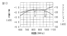
- the insertion loss characteristic from the first terminal 41 to the third terminal 43 is as shown by the curve X in FIG. 10
- the isolation characteristic from the first terminal 41 to the second terminal 42 is as shown by the curve Y in FIG. is there.
- the isolation characteristic is substantially flat in the operation bandwidth 698 to 960 MHz.
- the phase characteristic of isolation from the first terminal 41 to the second terminal 42 is not shown here, it is almost the same as the curve Z in FIG.
- the characteristic configuration of the fourth embodiment is that the other ends of the parallel resonant circuit composed of (L1, C1), (L2, C2), and (L3, C3) are connected together at one point,
- the connection point is connected to the ground via a series resonance circuit of (Lg, Cg)
- Cs3 is connected to the connection point between L3 and C3, Ls3 is further connected
- the other end of Ls3 is connected to the third terminal 43.
- C4 is connected to a connection point between one end of L3 and C3, and the other end of C4 is connected to the ground.
- the nonreciprocal circuit device according to the present invention is not limited to the above-described embodiment, and can be variously modified within the scope of the gist thereof.
- the configuration and shape of the central conductor are arbitrary.
- the inductance element and the capacitive element may be constituted by a conductor built in the circuit board in addition to being mounted on the circuit board as a chip type.
Abstract
Selon la présente invention, par rapport à un matériau magnétique à micro-ondes (20) sur lequel est appliqué un champ magnétique à courant continu au moyen d'un aimant permanent, un premier conducteur central (21), un deuxième conducteur central (22) et un troisième conducteur central (23) sont chacun disposés de manière à se croiser les uns les autres dans des états isolés. La présente invention traite une extrémité du premier conducteur central (21) en tant que premier accès (P1), une extrémité du deuxième conducteur central (22) en tant que deuxième accès (P2), et une extrémité du troisième conducteur central (23) en tant que troisième accès (P3). Un premier élément de capacité (C1) et monté en parallèle par rapport au premier conducteur central (21) ; un deuxième élément de capacité (C2) est monté en parallèle par rapport au deuxième conducteur central (22) ; chacune des autres extrémités du premier conducteur central (21) ; le deuxième conducteur central (22) et le troisième conducteur central (23) sont connectés l'un à l'autre et sont mis à la masse par l'intermédiaire d'un premier élément inductif (Lg) et d'un troisième élément de capacité (Cg) qui sont montés en série. Un deuxième élément inductif (LA) est monté en parallèle par rapport à une extrémité du conducteur central (23), tandis que l'autre extrémité du deuxième élément inductif (LA) est connectée à la masse. Un quatrième élément de capacité (Cs3) est connecté à un nœud de connexion entre la première extrémité du conducteur central (23) et le deuxième élément inductif (LA), tandis que l'autre extrémité du quatrième élément de capacité (Cs3) est connectée à une troisième borne (43).
Priority Applications (4)
| Application Number | Priority Date | Filing Date | Title |
|---|---|---|---|
| JP2014523651A JP5655990B2 (ja) | 2012-07-02 | 2013-06-04 | 非可逆回路素子 |
| CN201380026030.3A CN104303361B (zh) | 2012-07-02 | 2013-06-04 | 不可逆电路元件 |
| US14/540,342 US9112256B2 (en) | 2012-07-02 | 2014-11-13 | Non-reciprocal circuit element |
| US14/794,934 US9172125B1 (en) | 2012-07-02 | 2015-07-09 | Non-reciprocal circuit element |
Applications Claiming Priority (2)
| Application Number | Priority Date | Filing Date | Title |
|---|---|---|---|
| JP2012148282 | 2012-07-02 | ||
| JP2012-148282 | 2012-07-02 |
Related Child Applications (1)
| Application Number | Title | Priority Date | Filing Date |
|---|---|---|---|
| US14/540,342 Continuation US9112256B2 (en) | 2012-07-02 | 2014-11-13 | Non-reciprocal circuit element |
Publications (1)
| Publication Number | Publication Date |
|---|---|
| WO2014007014A1 true WO2014007014A1 (fr) | 2014-01-09 |
Family
ID=49881774
Family Applications (1)
| Application Number | Title | Priority Date | Filing Date |
|---|---|---|---|
| PCT/JP2013/065440 WO2014007014A1 (fr) | 2012-07-02 | 2013-06-04 | Élément de circuit non réciproque |
Country Status (3)
| Country | Link |
|---|---|
| US (2) | US9112256B2 (fr) |
| JP (1) | JP5655990B2 (fr) |
| WO (1) | WO2014007014A1 (fr) |
Cited By (1)
| Publication number | Priority date | Publication date | Assignee | Title |
|---|---|---|---|---|
| WO2017150619A1 (fr) * | 2016-03-03 | 2017-09-08 | 株式会社村田製作所 | Élément de circuit irréversible, circuit frontal et dispositif de communication |
Families Citing this family (1)
| Publication number | Priority date | Publication date | Assignee | Title |
|---|---|---|---|---|
| KR20160099397A (ko) | 2015-02-12 | 2016-08-22 | 삼성전자주식회사 | 제한된 실행 환경에서 결제 기능을 수행하기 위한 방법 및 장치 |
Citations (3)
| Publication number | Priority date | Publication date | Assignee | Title |
|---|---|---|---|---|
| JPH1098308A (ja) * | 1996-09-19 | 1998-04-14 | Murata Mfg Co Ltd | 非可逆回路素子 |
| JP2001053505A (ja) * | 1999-08-10 | 2001-02-23 | Murata Mfg Co Ltd | 非可逆回路素子、複合電子部品及び通信機装置 |
| JP2011055222A (ja) * | 2009-09-01 | 2011-03-17 | Murata Mfg Co Ltd | 非可逆回路素子 |
Family Cites Families (9)
| Publication number | Priority date | Publication date | Assignee | Title |
|---|---|---|---|---|
| JPS5232713B2 (fr) * | 1972-05-24 | 1977-08-23 | ||
| US3836874A (en) * | 1973-06-25 | 1974-09-17 | Hitachi Ltd | Lumped element circulator |
| JPH0720215Y2 (ja) | 1988-07-25 | 1995-05-15 | 東陶機器株式会社 | 分岐用管体付配管ユニット |
| JPH0613203U (ja) | 1992-01-17 | 1994-02-18 | 日立フェライト株式会社 | 集中定数型アイソレータおよびサーキュレータ |
| JP3399080B2 (ja) * | 1994-04-07 | 2003-04-21 | 株式会社村田製作所 | 非可逆回路素子 |
| CA2214617C (fr) | 1996-09-06 | 2000-12-19 | Toshihiro Makino | Circuit non reversible |
| JP3807071B2 (ja) * | 1997-12-08 | 2006-08-09 | Tdk株式会社 | 非可逆回路素子 |
| US6696901B1 (en) * | 1999-03-26 | 2004-02-24 | Hitachi Metals, Ltd. | Concentrated constant irreciprocal device |
| JP4097084B2 (ja) * | 2004-04-22 | 2008-06-04 | Tdk株式会社 | 非可逆回路素子 |
-
2013
- 2013-06-04 JP JP2014523651A patent/JP5655990B2/ja active Active
- 2013-06-04 WO PCT/JP2013/065440 patent/WO2014007014A1/fr active Application Filing
-
2014
- 2014-11-13 US US14/540,342 patent/US9112256B2/en active Active
-
2015
- 2015-07-09 US US14/794,934 patent/US9172125B1/en active Active
Patent Citations (3)
| Publication number | Priority date | Publication date | Assignee | Title |
|---|---|---|---|---|
| JPH1098308A (ja) * | 1996-09-19 | 1998-04-14 | Murata Mfg Co Ltd | 非可逆回路素子 |
| JP2001053505A (ja) * | 1999-08-10 | 2001-02-23 | Murata Mfg Co Ltd | 非可逆回路素子、複合電子部品及び通信機装置 |
| JP2011055222A (ja) * | 2009-09-01 | 2011-03-17 | Murata Mfg Co Ltd | 非可逆回路素子 |
Cited By (1)
| Publication number | Priority date | Publication date | Assignee | Title |
|---|---|---|---|---|
| WO2017150619A1 (fr) * | 2016-03-03 | 2017-09-08 | 株式会社村田製作所 | Élément de circuit irréversible, circuit frontal et dispositif de communication |
Also Published As
| Publication number | Publication date |
|---|---|
| US20150070101A1 (en) | 2015-03-12 |
| CN104303361A (zh) | 2015-01-21 |
| US9112256B2 (en) | 2015-08-18 |
| US20150311574A1 (en) | 2015-10-29 |
| US9172125B1 (en) | 2015-10-27 |
| JPWO2014007014A1 (ja) | 2016-06-02 |
| JP5655990B2 (ja) | 2015-01-21 |
Similar Documents
| Publication | Publication Date | Title |
|---|---|---|
| JP5679056B2 (ja) | 非可逆回路素子 | |
| JPWO2012020613A1 (ja) | 非可逆回路素子 | |
| JP5843007B2 (ja) | 非可逆回路素子 | |
| JP5655990B2 (ja) | 非可逆回路素子 | |
| JP5983859B2 (ja) | 非可逆回路素子及びモジュール | |
| WO2011118278A1 (fr) | Elément de circuit non réciproque | |
| JP5790787B2 (ja) | 非可逆回路素子及び送受信装置 | |
| WO2015156056A1 (fr) | Élément de circuit non réciproque et module haute fréquence | |
| JP5748025B2 (ja) | 非可逆回路素子 | |
| JP5672394B2 (ja) | 非可逆回路素子 | |
| JP6011911B2 (ja) | 非可逆回路素子 | |
| JP6249104B2 (ja) | 非可逆回路素子 | |
| JP5880738B2 (ja) | 2ポート型非可逆回路素子 | |
| KR100317276B1 (ko) | 집중 정수형 아이솔레이터 | |
| JP6152896B2 (ja) | 非可逆回路素子 | |
| WO2014115595A1 (fr) | Élément de circuit irréversible | |
| JPWO2016158044A1 (ja) | 非可逆回路素子、高周波回路及び通信装置 | |
| US20150303545A1 (en) | Non-reciprocal circuit element | |
| JP2012138719A (ja) | 非可逆回路素子及びフェライト・磁石素子 | |
| WO2007013252A1 (fr) | Élément de circuit irréversible, composants électroniques composites et dispositif de communication | |
| JP2004260652A (ja) | 非可逆回路素子 | |
| JP2012090141A (ja) | 非可逆回路素子 |
Legal Events
| Date | Code | Title | Description |
|---|---|---|---|
| 121 | Ep: the epo has been informed by wipo that ep was designated in this application |
Ref document number: 13812912 Country of ref document: EP Kind code of ref document: A1 |
|
| ENP | Entry into the national phase |
Ref document number: 2014523651 Country of ref document: JP Kind code of ref document: A |
|
| NENP | Non-entry into the national phase |
Ref country code: DE |
|
| 122 | Ep: pct application non-entry in european phase |
Ref document number: 13812912 Country of ref document: EP Kind code of ref document: A1 |