WO2014007014A1 - Non-reciprocal circuit element - Google Patents
Non-reciprocal circuit element Download PDFInfo
- Publication number
- WO2014007014A1 WO2014007014A1 PCT/JP2013/065440 JP2013065440W WO2014007014A1 WO 2014007014 A1 WO2014007014 A1 WO 2014007014A1 JP 2013065440 W JP2013065440 W JP 2013065440W WO 2014007014 A1 WO2014007014 A1 WO 2014007014A1
- Authority
- WO
- WIPO (PCT)
- Prior art keywords
- center conductor
- port
- terminal
- conductor
- capacitive element
- Prior art date
Links
Images


Classifications
-
- H—ELECTRICITY
- H01—ELECTRIC ELEMENTS
- H01P—WAVEGUIDES; RESONATORS, LINES, OR OTHER DEVICES OF THE WAVEGUIDE TYPE
- H01P1/00—Auxiliary devices
- H01P1/32—Non-reciprocal transmission devices
- H01P1/38—Circulators
- H01P1/383—Junction circulators, e.g. Y-circulators
-
- H—ELECTRICITY
- H01—ELECTRIC ELEMENTS
- H01P—WAVEGUIDES; RESONATORS, LINES, OR OTHER DEVICES OF THE WAVEGUIDE TYPE
- H01P1/00—Auxiliary devices
- H01P1/32—Non-reciprocal transmission devices
- H01P1/38—Circulators
- H01P1/383—Junction circulators, e.g. Y-circulators
- H01P1/387—Strip line circulators
-
- H—ELECTRICITY
- H01—ELECTRIC ELEMENTS
- H01F—MAGNETS; INDUCTANCES; TRANSFORMERS; SELECTION OF MATERIALS FOR THEIR MAGNETIC PROPERTIES
- H01F7/00—Magnets
- H01F7/02—Permanent magnets [PM]
Definitions
- the present invention relates to non-reciprocal circuit elements, and more particularly to non-reciprocal circuit elements such as isolators and circulators used in the microwave band.
- nonreciprocal circuit elements such as isolators and circulators have a characteristic of transmitting a signal only in a predetermined specific direction and not transmitting in a reverse direction. Utilizing this characteristic, for example, an isolator is used in a transmission circuit unit of a mobile communication device such as a mobile phone.
- the circulator S is mounted between the noise canceller NC and the antenna ANT.
- the circulator S cancels the noise in the reception band by rotating the phases of the signal input from the antenna ANT and the signal output from the noise canceller NC by 180 °. Since the amplitude characteristic of the noise canceller NC is almost flat, the isolation characteristic of the circulator S is required to be as flat as that.
- an isolator I is mounted between the power amplifier PA and the duplexer DPX. Part of the signal output from the power amplifier PA is input to the gain control circuit AGC via the capacitor C, and the output voltage is monitored.
- the gain control circuit AGC does not work correctly, and the output of the power amplifier PA cannot be accurately controlled. Therefore, the flatness of the isolation characteristic is also required in this case.
- an object of the present invention is to provide a non-reciprocal circuit device having substantially flattened isolation characteristics.
- the nonreciprocal circuit device is A microwave magnetic body to which a direct-current magnetic field is applied by a permanent magnet, the first center conductor, the second center conductor, and the third center conductor are respectively arranged in an insulated state, One end of the first center conductor is a first port, one end of the second center conductor is a second port, and one end of the third center conductor is a third port, The first port is connected to the first terminal, the second port is connected to the second terminal, the third port is connected to the third terminal, and the first capacitive element is connected in parallel to the first central conductor, A second capacitive element connected in parallel to the two central conductors; The other ends of the first center conductor, the second center conductor, and the third center conductor are connected to each other and connected to the ground via the first inductance element and the third capacitance element connected in series, A second inductance element is connected in parallel to one end of the third central conductor, and the other end of the second inductance element
- the non-reciprocal circuit device is A microwave magnetic body to which a direct-current magnetic field is applied by a permanent magnet, the first center conductor, the second center conductor, and the third center conductor are respectively arranged in an insulated state, One end of the first center conductor is a first port, one end of the second center conductor is a second port, and one end of the third center conductor is a third port, The first port is connected to the first terminal, the second port is connected to the second terminal, the third port is connected to the third terminal, and the first capacitive element is connected in parallel to the first central conductor, A second capacitive element connected in parallel to the two central conductors; The other ends of the first center conductor, the second center conductor, and the third center conductor are connected to each other and connected to the ground via the first inductance element and the third capacitance element connected in series, A second inductance element connected in parallel to the third central conductor; A fourth capacitive element is connected to a connection point between
- the non-reciprocal circuit device is A microwave magnetic body to which a direct-current magnetic field is applied by a permanent magnet, the first center conductor, the second center conductor, and the third center conductor are respectively arranged in an insulated state, One end of the first center conductor is a first port, one end of the second center conductor is a second port, and one end of the third center conductor is a third port, The first port is connected to the first terminal, the second port is connected to the second terminal, Connecting the first capacitive element in parallel to the first central conductor, connecting the second capacitive element in parallel to the second central conductor; The other ends of the first center conductor, the second center conductor, and the third center conductor are connected to each other and connected to the ground via the first inductance element and the third capacitance element connected in series, A second inductance element connected in parallel to the third central conductor; A fourth capacitive element is connected in series to a connection point between one end of the third center electrode and the second
- the non-reciprocal circuit device is A microwave magnetic body to which a direct-current magnetic field is applied by a permanent magnet, the first center conductor, the second center conductor, and the third center conductor are respectively arranged in an insulated state, One end of the first center conductor is a first port, one end of the second center conductor is a second port, and one end of the third center conductor is a third port, The first port is connected to the first terminal, the second port is connected to the second terminal, the third port is connected to the third terminal, and the first capacitive element is connected in parallel to the first central conductor, A second capacitive element connected in parallel to the two central conductors; The other ends of the first center conductor, the second center conductor, and the third center conductor are connected to each other and connected to the ground via the first inductance element and the third capacitance element connected in series, A fifth capacitive element is connected in parallel to the third central conductor; A fourth capacitive element is connected in series to a
- a sixth capacitive element is connected to a connection point between one end of the third central conductor and the fifth capacitive element, and the other end of the sixth capacitive element is connected to the ground; It is characterized by.
- the first center conductor, the second center conductor, and the third center conductor are crossed in an insulated state with ferrite to which a DC magnetic field is applied by a permanent magnet.
- the nonreciprocal circuit elements according to the first, second, and fourth modes function as a circulator.
- a high-frequency signal input from the second port is output from the first port
- a high-frequency signal input from the first port Is output from the third port
- the high-frequency signal input from the third port is output from the second port.
- the non-reciprocal circuit device according to the third form functions as an isolator, and for example, a high frequency signal input from the first port is output from the second port.
- the high-frequency signal input from the second port is not output to the first port because the third port terminates with a resistive element.
- the high-frequency signal input / output relationship is reversed by reversing the DC magnetic field applied from the permanent magnet.
- the second inductance element is connected in parallel with the third central conductor, so that the isolation characteristic is substantially flat over a wide band.
- the fifth capacitor element is connected in parallel with the third center conductor, and the sixth capacitor is connected to the connection point between the one end of the third center conductor and the fifth capacitor element. Since the elements are connected and the other end of the sixth capacitive element is connected to the ground, the isolation specification is substantially flat over a wide band.
- the nonreciprocal circuit device is a lumped constant three-port circulator having the equivalent circuit shown in FIG. That is, the first center conductor 21 (L1), the second center conductor 22 (L2), and the third center conductor 23 (L3) are applied to a microwave magnetic body (ferrite 20) to which a DC magnetic field is applied in the direction of arrow A by a permanent magnet.
- a microwave magnetic body ferrite 20
- a DC magnetic field is applied in the direction of arrow A by a permanent magnet.
- each of the center conductors 21, 22, and 23 is connected to each other and to the ground via an inductance element Lg and a capacitance element Cg connected in series.
- Capacitance elements C1 and C2 are connected in parallel to the first and second center conductors 21 and 22, respectively.
- An inductance element LA is connected in parallel to one end of the third central conductor 23, and the other end of the inductance element LA is connected to the ground.
- a capacitance element Cs3 for impedance matching is connected to a connection point between one end of the third center electrode 23 and the inductance element LA, and the other end of the capacitance element Cs3 is connected to the third terminal 43.
- an impedance matching capacitive element Cs1 is connected between the first port P1 and the first terminal 41, and an impedance matching capacitive element Cs2 is connected between the second port P2 and the second terminal 42. Has been.
- the three-port circulator composed of the above equivalent circuit includes a circuit board 30, a central conductor assembly 10, and a permanent magnet 25, as shown in FIG.
- the center conductor assembly 10 is formed by laminating insulator layers 11 and 12 on the upper surface of a rectangular microwave ferrite 20.
- the first center conductor 21 is formed on the upper surface of the insulator layer 11, and both end portions thereof are via holes.
- a conductor 15 a and a via hole conductor 15 b formed in the ferrite 20 are led out to the lower surface side of the ferrite 20.
- the second center conductor 22 is formed on the upper surface of the insulator layer 12, and both ends thereof are via-hole conductors 15 c, via-hole conductors 15 d formed in the insulator layer 11, and via-hole conductors 15 e formed in the ferrite 20. It is pulled out to the lower surface side.
- the third center conductor 23 is formed on the upper surface of the ferrite 20, and is drawn out to the lower surface side of the ferrite 20 by a via-hole conductor 15 f.
- the center conductors 21, 22, and 23 can be formed on the ferrite 20 and the insulator layers 11 and 12 as a thin film conductor, a thick film conductor, or a conductor foil. In addition, various capacitive elements and inductance elements use chip parts.
- the central conductors 21, 22, and 23 may be wound in a coil shape by increasing the number of insulating layers.
- the ends of the center conductors 21, 22, and 23 and electrodes 31a to 31o for mounting various chip-type capacitance elements and inductance elements are formed.
- the 3-port circulator having the equivalent circuit shown in FIG. 1 is formed.
- a first terminal 41, a second terminal 42, and a third terminal 43 are formed on the lower surface of the circuit board 30.
- the high-frequency signal input from the second terminal 42 is output from the first terminal 41 (first port P1), and the first terminal 41 (first port P1).
- the high frequency signal input from the first port P1) is output from the third terminal 43 (third port P3), and the high frequency signal input from the third terminal 43 (third port P3) is the second terminal 42 (second port). P2).
- the application direction of the magnetic field to the ferrite 20 is reversed, the transmission path of the high-frequency signal is switched.
- the insertion loss characteristic from the second terminal 42 to the first terminal 41 is as shown by the curve X in FIG. 3, and the isolating characteristic from the first terminal 41 to the second terminal 42 is as follows. 3 is as indicated by the curve Y in FIG.
- the isolation characteristic the in-band deviation in the operation bandwidth 698 to 960 MHz is substantially flat about ⁇ 0.6 dB.
- the phase characteristic of isolation from the first terminal 41 to the second terminal 42 is substantially a straight line as shown by a curve Z in FIG. This phase characteristic is substantially the same as the phase characteristic of the noise canceller NC shown in FIG.
- the characteristic configuration in the first embodiment is that the parallel resonance circuit composed of (L1, C1) and (L2, C2) and the other ends of L3 are connected together to one point, and the connection point is (Lg, Cg) connected to the ground via a series resonant circuit, LA connected in parallel with L3, the other end of LA connected to the ground, and Cs3 at the connection point between L3 and LA.
- the other end of Cs3 is connected to the third terminal 43.
- the nonreciprocal circuit device is a lumped constant type three-port circulator having the equivalent circuit shown in FIG. Basically, it has the same circuit configuration as that of the first embodiment, and is different in that the other end of the inductance element LA is connected to the other end of the third central conductor 23 (L3).
- the specific configuration of the central conductors 21, 22, and 23 is basically the same as the perspective view shown in FIG.
- the operation mode in the second embodiment is basically the same as that in the first embodiment, and has the same effect.
- the insertion loss characteristic from the second terminal 42 to the first terminal 41 is as shown by the curve X in FIG. 6, and the isolation characteristic from the first terminal 41 to the second terminal 42 is as shown by the curve Y in FIG. is there.
- the isolation characteristic is substantially flat in the operation bandwidth 698 to 960 MHz.
- the phase characteristic of isolation from the first terminal 41 to the second terminal 42 is substantially a straight line as shown by a curve Z in FIG.
- the characteristic configuration of the second embodiment is that the other ends of the parallel resonant circuit composed of (L1, C1) and (L2, C2) and the parallel circuit of (L3, LA) are combined into one point.
- the connection point is connected to the ground via a series resonance circuit of (Lg, Cg), Cs3 is connected to the connection point between L3 and LA, and the other end of Cs3 is connected to the third terminal 43.
- the isolation characteristic from the first terminal 41 to the second terminal 42 is substantially flat.
- the nonreciprocal circuit device is a lumped constant type isolator having the equivalent circuit shown in FIG. Basically, it has the same circuit configuration as that of the second embodiment, and is different in that a resistance element R is connected in series to the capacitive element Cs3, and an end of the resistance element R is connected to the ground. That is, the third port P3 is terminated by the resistance element R.
- the high frequency signal input from the first terminal 41 (first port P1) is output from the second terminal 42 (second port P2).
- the high-frequency signal input from the second terminal 42 (second port P2) is not output to the first terminal 41 (first port P1) because the third port P3 is terminated by the resistance element R.
- the insertion loss characteristic from the first terminal 41 to the second terminal 42 and the isolation characteristic from the second terminal 42 to the first terminal 41 in the third embodiment are substantially the same as those in FIG. 6 shown in the second embodiment.
- the isolation characteristic is substantially flat in the operation bandwidth 698 to 960 MHz.
- the phase characteristic of isolation from the second terminal 42 to the first terminal 41 is substantially the same as that shown in FIG. 7 in the second embodiment.
- the characteristic configuration in the third embodiment is that the other ends of the parallel resonant circuit composed of (L1, C1) and (L2, C2) and the parallel circuit of (L3, LA) are combined into one point.
- the connection point is connected to the ground via a series resonance circuit of (Lg, Cg), Cs3 is connected to the connection point between L3 and LA, and the termination resistance element R is connected to Cs3. .
- the isolation characteristic from the second terminal 42 to the first terminal 41 is substantially flat.
- the nonreciprocal circuit device is a lumped constant three-port circulator having the equivalent circuit shown in FIG. Basically, it has the same circuit configuration as that of the second embodiment, except that a capacitive element C3 is connected instead of the inductance element LA shown in the second embodiment, and one end of the third center electrode 23 and the capacitance
- the capacitive element Cs3 is connected in series to the connection point with the element C3, the inductance element Ls3 is further connected in series, the other end of the inductance element Ls3 is connected to the third terminal 43, and the third central conductor 23
- the capacitive element C4 is connected to a connection point between one end and the capacitive element C3, and the other end of the capacitive element C4 is connected to the ground.
- the specific configuration of the central conductors 21, 22, and 23 is basically the same as the perspective view shown in FIG.
- the operation mode of the fourth embodiment is basically the same as that of the first embodiment, and provides the same operational effects.
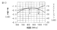
- the insertion loss characteristic from the first terminal 41 to the third terminal 43 is as shown by the curve X in FIG. 10
- the isolation characteristic from the first terminal 41 to the second terminal 42 is as shown by the curve Y in FIG. is there.
- the isolation characteristic is substantially flat in the operation bandwidth 698 to 960 MHz.
- the phase characteristic of isolation from the first terminal 41 to the second terminal 42 is not shown here, it is almost the same as the curve Z in FIG.
- the characteristic configuration of the fourth embodiment is that the other ends of the parallel resonant circuit composed of (L1, C1), (L2, C2), and (L3, C3) are connected together at one point,
- the connection point is connected to the ground via a series resonance circuit of (Lg, Cg)
- Cs3 is connected to the connection point between L3 and C3, Ls3 is further connected
- the other end of Ls3 is connected to the third terminal 43.
- C4 is connected to a connection point between one end of L3 and C3, and the other end of C4 is connected to the ground.
- the nonreciprocal circuit device according to the present invention is not limited to the above-described embodiment, and can be variously modified within the scope of the gist thereof.
- the configuration and shape of the central conductor are arbitrary.
- the inductance element and the capacitive element may be constituted by a conductor built in the circuit board in addition to being mounted on the circuit board as a chip type.
Abstract
With respect to a microwave magnetic material (20) to which a direct-current magnetic field is applied by way of a permanent magnet, a first center conductor (21), a second center conductor (22), and a third center conductor (23) are each disposed so as to cross one another in insulated states. The invention treats one end of the first center conductor (21) as a first port (P1), one end of the second center conductor (22) as a second port (P2), and one end of the third center conductor (23) as a third port (P3). A first capacitance element (C1) is connected in parallel with respect to the first center conductor (21); a second capacitance element (C2) is connected in parallel with respect to the second center conductor (22); each of the other ends of the first center conductor (21); the second center conductor (22), and the third center conductor (23) are connected to one another, and are grounded via a first inductive element (Lg) and a third capacitance element (Cg) which are serially connected. A second inductive element (LA) is connected in parallel with respect to one end of the center conductor (23), whereas the other end of the second inductive element (LA) is connected to a ground. A fourth capacitance element (Cs3) is connected to a connection node between the one end of the center conductor (23) and the second inductive element (LA), whereas the other end of the fourth capacitance element (Cs3) is connected to a third terminal (43).
Description
本発明は、非可逆回路素子、特に、マイクロ波帯で使用されるアイソレータやサーキュレータなどの非可逆回路素子に関する。
The present invention relates to non-reciprocal circuit elements, and more particularly to non-reciprocal circuit elements such as isolators and circulators used in the microwave band.
従来より、アイソレータやサーキュレータなどの非可逆回路素子は、予め定められた特定方向にのみ信号を伝送し、逆方向には伝送しない特性を有している。この特性を利用して、例えば、アイソレータは、携帯電話などの移動体通信機器の送信回路部に使用されている。
Conventionally, nonreciprocal circuit elements such as isolators and circulators have a characteristic of transmitting a signal only in a predetermined specific direction and not transmitting in a reverse direction. Utilizing this characteristic, for example, an isolator is used in a transmission circuit unit of a mobile communication device such as a mobile phone.
この種の非可逆回路素子であって、3端子タイプのサーキュレータとしては特許文献1,2に記載のものが知られている。そのアイソレーション特性は、特許文献1の図2、特許文献2の第5図に示されているように、単峰性を有している。しかし、サーキュレータやアイソレータが使用される回路によっては、平坦性を有するアイソレーション特性が求められる場合があり、この種のサーキュレータやアイソレータでは対応できないという問題点を有している。
As this type of nonreciprocal circuit device, those described in Patent Documents 1 and 2 are known as three-terminal type circulators. The isolation characteristics are unimodal as shown in FIG. 2 of Patent Document 1 and FIG. 5 of Patent Document 2. However, depending on the circuit in which the circulator or isolator is used, there is a case where flat isolation characteristics are required, and this type of circulator or isolator has a problem that it cannot cope with it.
例えば、図11に示す無線通信装置100にあっては、ノイズキャンセラーNCとアンテナANTとの間にサーキュレータSが搭載される。このサーキュレータSはアンテナANTから入力された信号とノイズキャンセラーNCから出力される信号の位相を互いに180°回転させて受信帯域のノイズを相殺する。ノイズキャンセラーNCの振幅特性はほぼ平坦なのでサーキュレータSのアイソレーション特性もそれと同じ程度の平坦性が求められる。
For example, in the wireless communication apparatus 100 shown in FIG. 11, the circulator S is mounted between the noise canceller NC and the antenna ANT. The circulator S cancels the noise in the reception band by rotating the phases of the signal input from the antenna ANT and the signal output from the noise canceller NC by 180 °. Since the amplitude characteristic of the noise canceller NC is almost flat, the isolation characteristic of the circulator S is required to be as flat as that.
また、図12に示す携帯電話のRF回路150にあっては、パワーアンプPAとデュープレクサDPXとの間にアイソレータIが搭載される。パワーアンプPAから出力される信号の一部をコンデンサCを介してゲインコントロール回路AGCに入力させ、出力電圧をモニターしている。アンテナANTからの反射が大きい場合で、アイソレータIのアイソレーション特性が小さくかつ平坦でなく、周波数特性が大きい場合は、パワーアンプPAから出力された電力の大きさを正確に検出できない。それゆえ、ゲインコントロール回路AGCが正確に働かず、パワーアンプPAの出力を正確に制御できないことになる。従って、この場合にもアイソレーション特性の平坦性が求められる。
In the mobile phone RF circuit 150 shown in FIG. 12, an isolator I is mounted between the power amplifier PA and the duplexer DPX. Part of the signal output from the power amplifier PA is input to the gain control circuit AGC via the capacitor C, and the output voltage is monitored. When the reflection from the antenna ANT is large, and the isolation characteristic of the isolator I is small and not flat and the frequency characteristic is large, the magnitude of the power output from the power amplifier PA cannot be detected accurately. Therefore, the gain control circuit AGC does not work correctly, and the output of the power amplifier PA cannot be accurately controlled. Therefore, the flatness of the isolation characteristic is also required in this case.
そこで、本発明の目的は、アイソレーション特性がほぼ平坦化された非可逆回路素子を提供することにある。
Accordingly, an object of the present invention is to provide a non-reciprocal circuit device having substantially flattened isolation characteristics.
本発明の第1の形態である非可逆回路素子は、
永久磁石により直流磁界が印加されるマイクロ波磁性体に第1中心導体、第2中心導体及び第3中心導体をそれぞれ絶縁状態で交差させて配置し、
第1中心導体の一端を第1ポート、第2中心導体の一端を第2ポート、第3中心導体の一端を第3ポートとし、
第1ポートは第1端子に接続され、第2ポートは第2端子に接続され、第3ポートは第3端子に接続され
第1中心導体に対して第1容量素子を並列に接続し、第2中心導体に対して第2容量素子を並列に接続し、
第1中心導体、第2中心導体及び第3中心導体のそれぞれの他端は互いに接続されるとともに、直列に接続された第1インダクタンス素子と第3容量素子とを介してグランドに接続され、
第3中心導体の一端に対して第2インダクタンス素子を並列に接続し、該第2インダクタンス素子の他端はグランドに接続され、
第3中心電極の一端と第2インダクタンス素子との接続点に第4容量素子を接続し、該第4容量素子の他端は第3端子に接続されていること、
を特徴とする。 The nonreciprocal circuit device according to the first aspect of the present invention is
A microwave magnetic body to which a direct-current magnetic field is applied by a permanent magnet, the first center conductor, the second center conductor, and the third center conductor are respectively arranged in an insulated state,
One end of the first center conductor is a first port, one end of the second center conductor is a second port, and one end of the third center conductor is a third port,
The first port is connected to the first terminal, the second port is connected to the second terminal, the third port is connected to the third terminal, and the first capacitive element is connected in parallel to the first central conductor, A second capacitive element connected in parallel to the two central conductors;
The other ends of the first center conductor, the second center conductor, and the third center conductor are connected to each other and connected to the ground via the first inductance element and the third capacitance element connected in series,
A second inductance element is connected in parallel to one end of the third central conductor, and the other end of the second inductance element is connected to the ground,
A fourth capacitive element is connected to a connection point between one end of the third central electrode and the second inductance element, and the other end of the fourth capacitive element is connected to the third terminal;
It is characterized by.
本発明の第2の形態である非可逆回路素子は、
永久磁石により直流磁界が印加されるマイクロ波磁性体に第1中心導体、第2中心導体及び第3中心導体をそれぞれ絶縁状態で交差させて配置し、
第1中心導体の一端を第1ポート、第2中心導体の一端を第2ポート、第3中心導体の一端を第3ポートとし、
第1ポートは第1端子に接続され、第2ポートは第2端子に接続され、第3ポートは第3端子に接続され
第1中心導体に対して第1容量素子を並列に接続し、第2中心導体に対して第2容量素子を並列に接続し、
第1中心導体、第2中心導体及び第3中心導体のそれぞれの他端は互いに接続されるとともに、直列に接続された第1インダクタンス素子と第3容量素子とを介してグランドに接続され、
第3中心導体に対して第2インダクタンス素子を並列に接続し、
第3中心電極の一端と第2インダクタンス素子との接続点に第4容量素子を接続し、該第4容量素子の他端は第3端子に接続されていること、
を特徴とする。 The non-reciprocal circuit device according to the second aspect of the present invention is
A microwave magnetic body to which a direct-current magnetic field is applied by a permanent magnet, the first center conductor, the second center conductor, and the third center conductor are respectively arranged in an insulated state,
One end of the first center conductor is a first port, one end of the second center conductor is a second port, and one end of the third center conductor is a third port,
The first port is connected to the first terminal, the second port is connected to the second terminal, the third port is connected to the third terminal, and the first capacitive element is connected in parallel to the first central conductor, A second capacitive element connected in parallel to the two central conductors;
The other ends of the first center conductor, the second center conductor, and the third center conductor are connected to each other and connected to the ground via the first inductance element and the third capacitance element connected in series,
A second inductance element connected in parallel to the third central conductor;
A fourth capacitive element is connected to a connection point between one end of the third central electrode and the second inductance element, and the other end of the fourth capacitive element is connected to the third terminal;
It is characterized by.
本発明の第3の形態である非可逆回路素子は、
永久磁石により直流磁界が印加されるマイクロ波磁性体に第1中心導体、第2中心導体及び第3中心導体をそれぞれ絶縁状態で交差させて配置し、
第1中心導体の一端を第1ポート、第2中心導体の一端を第2ポート、第3中心導体の一端を第3ポートとし、
第1ポートは第1端子に接続され、第2ポートは第2端子に接続され、
第1中心導体に対して第1容量素子を並列に接続し、第2中心導体に対して第2容量素子を並列に接続し、
第1中心導体、第2中心導体及び第3中心導体のそれぞれの他端は互いに接続されるとともに、直列に接続された第1インダクタンス素子と第3容量素子とを介してグランドに接続され、
第3中心導体に対して第2インダクタンス素子を並列に接続し、
第3中心電極の一端と第2インダクタンス素子との接続点に第4容量素子を直列に接続し、さらに抵抗素子を直列に接続し、該抵抗素子の他端はグランドに接続されていること、
を特徴とする。 The non-reciprocal circuit device according to the third aspect of the present invention is
A microwave magnetic body to which a direct-current magnetic field is applied by a permanent magnet, the first center conductor, the second center conductor, and the third center conductor are respectively arranged in an insulated state,
One end of the first center conductor is a first port, one end of the second center conductor is a second port, and one end of the third center conductor is a third port,
The first port is connected to the first terminal, the second port is connected to the second terminal,
Connecting the first capacitive element in parallel to the first central conductor, connecting the second capacitive element in parallel to the second central conductor;
The other ends of the first center conductor, the second center conductor, and the third center conductor are connected to each other and connected to the ground via the first inductance element and the third capacitance element connected in series,
A second inductance element connected in parallel to the third central conductor;
A fourth capacitive element is connected in series to a connection point between one end of the third center electrode and the second inductance element, a resistance element is connected in series, and the other end of the resistance element is connected to the ground;
It is characterized by.
本発明の第4の形態である非可逆回路素子は、
永久磁石により直流磁界が印加されるマイクロ波磁性体に第1中心導体、第2中心導体及び第3中心導体をそれぞれ絶縁状態で交差させて配置し、
第1中心導体の一端を第1ポート、第2中心導体の一端を第2ポート、第3中心導体の一端を第3ポートとし、
第1ポートは第1端子に接続され、第2ポートは第2端子に接続され、第3ポートは第3端子に接続され
第1中心導体に対して第1容量素子を並列に接続し、第2中心導体に対して第2容量素子を並列に接続し、
第1中心導体、第2中心導体及び第3中心導体のそれぞれの他端は互いに接続されるとともに、直列に接続された第1インダクタンス素子と第3容量素子とを介してグランドに接続され、
第3中心導体に対して第5容量素子を並列に接続し、
第3中心電極の一端と第5容量素子との接続点に第4容量素子を直列に接続し、さらに第3インダクタンス素子を直列に接続し、該第3インダクタンス素子の他端は第3端子に接続され、
第3中心導体の一端と第5容量素子との接続点に第6容量素子を接続し、該第6容量素子の他端はグランドに接続されていること、
を特徴とする。 The non-reciprocal circuit device according to the fourth aspect of the present invention is
A microwave magnetic body to which a direct-current magnetic field is applied by a permanent magnet, the first center conductor, the second center conductor, and the third center conductor are respectively arranged in an insulated state,
One end of the first center conductor is a first port, one end of the second center conductor is a second port, and one end of the third center conductor is a third port,
The first port is connected to the first terminal, the second port is connected to the second terminal, the third port is connected to the third terminal, and the first capacitive element is connected in parallel to the first central conductor, A second capacitive element connected in parallel to the two central conductors;
The other ends of the first center conductor, the second center conductor, and the third center conductor are connected to each other and connected to the ground via the first inductance element and the third capacitance element connected in series,
A fifth capacitive element is connected in parallel to the third central conductor;
A fourth capacitive element is connected in series to a connection point between one end of the third center electrode and the fifth capacitive element, and a third inductance element is connected in series. The other end of the third inductance element is connected to the third terminal. Connected,
A sixth capacitive element is connected to a connection point between one end of the third central conductor and the fifth capacitive element, and the other end of the sixth capacitive element is connected to the ground;
It is characterized by.
前記非可逆回路素子は、永久磁石により直流磁界が印加されるフェライトに第1中心導体、第2中心導体及び第3中心導体をそれぞれ絶縁状態で交差させている。第1、第2及び第4の形態である非可逆回路素子はサーキュレータとして機能し、例えば、第2ポートから入力された高周波信号は第1ポートから出力され、第1ポートから入力された高周波信号は第3ポートから出力され、第3ポートから入力された高周波信号は第2ポートから出力される。第3形態である非可逆回路素子はアイソレータとして機能し、例えば、第1ポートから入力された高周波信号は第2ポートから出力される。一方、第2ポートから入力された高周波信号は第3ポートが抵抗素子で終端しているため、第1ポートに対して出力されない。
In the nonreciprocal circuit element, the first center conductor, the second center conductor, and the third center conductor are crossed in an insulated state with ferrite to which a DC magnetic field is applied by a permanent magnet. The nonreciprocal circuit elements according to the first, second, and fourth modes function as a circulator. For example, a high-frequency signal input from the second port is output from the first port, and a high-frequency signal input from the first port Is output from the third port, and the high-frequency signal input from the third port is output from the second port. The non-reciprocal circuit device according to the third form functions as an isolator, and for example, a high frequency signal input from the first port is output from the second port. On the other hand, the high-frequency signal input from the second port is not output to the first port because the third port terminates with a resistive element.
なお、高周波信号の入出力関係は、永久磁石から印加される直流磁界を反転させることにより、逆転する。
The high-frequency signal input / output relationship is reversed by reversing the DC magnetic field applied from the permanent magnet.
第1、第2及び第3の形態である非可逆回路素子では、第3中心導体と並列に第2インダクタンス素子が接続されていることから、アイソレーション特性が広帯域にわたってほぼ平坦になる。また、第4の形態である非可逆回路素子では、第3中心導体と並列に第5容量素子を接続し、かつ、第3中心導体の一端と第5容量素子との接続点に第6容量素子を接続し、該第6容量素子の他端がグランドに接続されていることから、アイソレーション特定が広帯域にわたってほぼ平坦になる。
In the non-reciprocal circuit elements according to the first, second, and third forms, the second inductance element is connected in parallel with the third central conductor, so that the isolation characteristic is substantially flat over a wide band. In the nonreciprocal circuit device according to the fourth aspect, the fifth capacitor element is connected in parallel with the third center conductor, and the sixth capacitor is connected to the connection point between the one end of the third center conductor and the fifth capacitor element. Since the elements are connected and the other end of the sixth capacitive element is connected to the ground, the isolation specification is substantially flat over a wide band.
本発明によれば、アイソレーション特性がほぼ平坦化された非可逆回路素子を得ることができる。
According to the present invention, it is possible to obtain a non-reciprocal circuit element having substantially flattened isolation characteristics.
以下に、本発明に係る非可逆回路素子の実施例について添付図面を参照して説明する。なお、各図において同じ部材には共通する符号を付し、重複する説明は省略する。
Hereinafter, embodiments of the non-reciprocal circuit device according to the present invention will be described with reference to the accompanying drawings. In addition, in each figure, the same code | symbol is attached | subjected to the same member, and the overlapping description is abbreviate | omitted.
(第1実施例、図1~図4参照)
第1実施例である非可逆回路素子は、図1に示す等価回路を有する集中定数型の3ポート型サーキュレータである。即ち、永久磁石により矢印A方向に直流磁界が印加されるマイクロ波磁性体(フェライト20)に第1中心導体21(L1)、第2中心導体22(L2)及び第3中心導体23(L3)をそれぞれ絶縁状態で所定の角度で交差させて配置し、第1中心導体21の一端を第1ポートP1、第2中心導体の一端を第2ポートP2、第3中心導体23の一端を第3ポートP3としている。 (Refer to the first embodiment, FIGS. 1 to 4)
The nonreciprocal circuit device according to the first embodiment is a lumped constant three-port circulator having the equivalent circuit shown in FIG. That is, the first center conductor 21 (L1), the second center conductor 22 (L2), and the third center conductor 23 (L3) are applied to a microwave magnetic body (ferrite 20) to which a DC magnetic field is applied in the direction of arrow A by a permanent magnet. Are arranged so as to cross each other at a predetermined angle in an insulated state, one end of thefirst center conductor 21 is the first port P1, one end of the second center conductor is the second port P2, and one end of the third center conductor 23 is the third port. Port P3 is set.
第1実施例である非可逆回路素子は、図1に示す等価回路を有する集中定数型の3ポート型サーキュレータである。即ち、永久磁石により矢印A方向に直流磁界が印加されるマイクロ波磁性体(フェライト20)に第1中心導体21(L1)、第2中心導体22(L2)及び第3中心導体23(L3)をそれぞれ絶縁状態で所定の角度で交差させて配置し、第1中心導体21の一端を第1ポートP1、第2中心導体の一端を第2ポートP2、第3中心導体23の一端を第3ポートP3としている。 (Refer to the first embodiment, FIGS. 1 to 4)
The nonreciprocal circuit device according to the first embodiment is a lumped constant three-port circulator having the equivalent circuit shown in FIG. That is, the first center conductor 21 (L1), the second center conductor 22 (L2), and the third center conductor 23 (L3) are applied to a microwave magnetic body (ferrite 20) to which a DC magnetic field is applied in the direction of arrow A by a permanent magnet. Are arranged so as to cross each other at a predetermined angle in an insulated state, one end of the
さらに、各中心導体21,22,23のそれぞれの他端は互いに接続されるとともに直列に接続されたインダクタンス素子Lgと容量素子Cgを介してグランドに接続されている。第1及び第2中心導体21,22に対して並列に容量素子C1,C2がそれぞれ接続されている。第3中心導体23の一端に対してインダクタンス素子LAが並列に接続され、該インダクタンス素子LAの他端はグランドに接続されている。第3中心電極23の一端とインダクタンス素子LAとの接続点にはインピーダンス整合用の容量素子Cs3が接続され、該容量素子Cs3の他端は第3端子43に接続されている。
Furthermore, the other end of each of the center conductors 21, 22, and 23 is connected to each other and to the ground via an inductance element Lg and a capacitance element Cg connected in series. Capacitance elements C1 and C2 are connected in parallel to the first and second center conductors 21 and 22, respectively. An inductance element LA is connected in parallel to one end of the third central conductor 23, and the other end of the inductance element LA is connected to the ground. A capacitance element Cs3 for impedance matching is connected to a connection point between one end of the third center electrode 23 and the inductance element LA, and the other end of the capacitance element Cs3 is connected to the third terminal 43.
さらに、第1ポートP1と第1端子41との間にはインピーダンス整合用の容量素子Cs1が接続され、第2ポートP2と第2端子42との間にはインピーダンス整合用の容量素子Cs2が接続されている。
Further, an impedance matching capacitive element Cs1 is connected between the first port P1 and the first terminal 41, and an impedance matching capacitive element Cs2 is connected between the second port P2 and the second terminal 42. Has been.
以上の等価回路からなる3ポート型サーキュレータは、具体的には、図2に示すように、回路基板30と、中心導体組立体10と、永久磁石25と、で構成されている。
Specifically, the three-port circulator composed of the above equivalent circuit includes a circuit board 30, a central conductor assembly 10, and a permanent magnet 25, as shown in FIG.
中心導体組立体10は、矩形状のマイクロ波フェライト20の上面に絶縁体層11,12を積層したもので、第1中心導体21は絶縁体層11の上面に形成され、その両端部はビアホール導体15a及びフェライト20に形成されたビアホール導体15bを介してフェライト20の下面側に引き出されている。第2中心導体22は絶縁体層12の上面に形成され、その両端部はビアホール導体15c、絶縁体層11に形成されたビアホール導体15d及びフェライト20に形成されたビアホール導体15eを介してフェライト20の下面側に引き出されている。第3中心導体23はフェライト20の上面に形成され、ビアホール導体15fにてフェライト20の下面側に引き出されている。
The center conductor assembly 10 is formed by laminating insulator layers 11 and 12 on the upper surface of a rectangular microwave ferrite 20. The first center conductor 21 is formed on the upper surface of the insulator layer 11, and both end portions thereof are via holes. A conductor 15 a and a via hole conductor 15 b formed in the ferrite 20 are led out to the lower surface side of the ferrite 20. The second center conductor 22 is formed on the upper surface of the insulator layer 12, and both ends thereof are via-hole conductors 15 c, via-hole conductors 15 d formed in the insulator layer 11, and via-hole conductors 15 e formed in the ferrite 20. It is pulled out to the lower surface side. The third center conductor 23 is formed on the upper surface of the ferrite 20, and is drawn out to the lower surface side of the ferrite 20 by a via-hole conductor 15 f.
中心導体21,22,23はフェライト20や絶縁体層11,12上に薄膜導体、厚膜導体、又は、導体箔として形成することができる。また、各種容量素子やインダクタンス素子はチップ部品を使用している。なお、中心導体21,22,23は絶縁体層の積層数を増加させてコイル状に巻き回したものであってもよい。
The center conductors 21, 22, and 23 can be formed on the ferrite 20 and the insulator layers 11 and 12 as a thin film conductor, a thick film conductor, or a conductor foil. In addition, various capacitive elements and inductance elements use chip parts. The central conductors 21, 22, and 23 may be wound in a coil shape by increasing the number of insulating layers.
回路基板30は、その上面に、各中心導体21,22,23の端部やチップタイプの各種容量素子及びインダクタンス素子を実装するための電極31a~31oが形成され、中心導体組立体10及び永久磁石25を積み重ねて回路基板30上に実装することにより、図1に示す等価回路の3ポート型サーキュレータが形成される。また、回路基板30の下面には、図示されていないが、第1端子41、第2端子42及び第3端子43が形成されている。
On the upper surface of the circuit board 30, the ends of the center conductors 21, 22, and 23 and electrodes 31a to 31o for mounting various chip-type capacitance elements and inductance elements are formed. By stacking the magnets 25 and mounting them on the circuit board 30, the 3-port circulator having the equivalent circuit shown in FIG. 1 is formed. Although not shown, a first terminal 41, a second terminal 42, and a third terminal 43 are formed on the lower surface of the circuit board 30.
第1実施例である3ポート型サーキュレータにおいて、第2端子42(第2ポートP2)から入力された高周波信号は、第1端子41(第1ポートP1)から出力され、第1端子41(第1ポートP1)から入力された高周波信号は第3端子43(第3ポートP3)から出力され、第3端子43(第3ポートP3)から入力された高周波信号は第2端子42(第2ポートP2)から出力される。但し、フェライト20への磁界の印加方向を逆にすると、高周波信号の伝達経路が入れ替わる。
In the three-port circulator according to the first embodiment, the high-frequency signal input from the second terminal 42 (second port P2) is output from the first terminal 41 (first port P1), and the first terminal 41 (first port P1). The high frequency signal input from the first port P1) is output from the third terminal 43 (third port P3), and the high frequency signal input from the third terminal 43 (third port P3) is the second terminal 42 (second port). P2). However, if the application direction of the magnetic field to the ferrite 20 is reversed, the transmission path of the high-frequency signal is switched.
第1実施例である3ポート型サーキュレータにおいて、第2端子42から第1端子41への挿入損失特性は図3の曲線Xに示すとおりであり、第1端子41から第2端子42へのアイソレーション特性は図3の曲線Yに示すとおりである。アイソレーション特性では動作帯域幅698~960MHzにおける帯域内偏差が±0.6dB程度にほぼ平坦な特性となっている。また、第1端子41から第2端子42へのアイソレーションの位相特性は図4の曲線Zに示すようにほぼ直線になっている。この位相特性は、図11に示すノイズキャンセラーNCの位相特性とほぼ同じである。
In the three-port circulator according to the first embodiment, the insertion loss characteristic from the second terminal 42 to the first terminal 41 is as shown by the curve X in FIG. 3, and the isolating characteristic from the first terminal 41 to the second terminal 42 is as follows. 3 is as indicated by the curve Y in FIG. In the isolation characteristic, the in-band deviation in the operation bandwidth 698 to 960 MHz is substantially flat about ± 0.6 dB. Further, the phase characteristic of isolation from the first terminal 41 to the second terminal 42 is substantially a straight line as shown by a curve Z in FIG. This phase characteristic is substantially the same as the phase characteristic of the noise canceller NC shown in FIG.
本第1実施例での特徴的構成は、(L1,C1)と(L2,C2)からなる並列共振回路、及び、L3のそれぞれの他端をまとめて1点に接続し、該接続点を(Lg,Cg)の直列共振回路を介してグランドに接続したこと、L3と並列にLAを接続し、LAの他端をグランドに接続したこと、さらに、L3とLAとの接続点にCs3を接続し、Cs3の他端を第3端子43に接続したことにある。このような特徴的構成によって、第1端子41から第2端子42へのアイソレーション特性がほぼ平坦な特性となっている。
The characteristic configuration in the first embodiment is that the parallel resonance circuit composed of (L1, C1) and (L2, C2) and the other ends of L3 are connected together to one point, and the connection point is (Lg, Cg) connected to the ground via a series resonant circuit, LA connected in parallel with L3, the other end of LA connected to the ground, and Cs3 at the connection point between L3 and LA. The other end of Cs3 is connected to the third terminal 43. With such a characteristic configuration, the isolation characteristic from the first terminal 41 to the second terminal 42 is substantially flat.
(第2実施例、図5~図7参照)
第2実施例である非可逆回路素子は、図5に示す等価回路を有する集中定数型の3ポート型サーキュレータである。基本的には前記第1実施例と同じ回路構成を有し、異なるのは、インダクタンス素子LAの他端を第3中心導体23(L3)の他端に接続した点である。中心導体21,22,23の具体的な構成は図2に示した斜視図と基本的に同じである。 (Refer to the second embodiment, FIGS. 5 to 7)
The nonreciprocal circuit device according to the second embodiment is a lumped constant type three-port circulator having the equivalent circuit shown in FIG. Basically, it has the same circuit configuration as that of the first embodiment, and is different in that the other end of the inductance element LA is connected to the other end of the third central conductor 23 (L3). The specific configuration of the central conductors 21, 22, and 23 is basically the same as the perspective view shown in FIG.
第2実施例である非可逆回路素子は、図5に示す等価回路を有する集中定数型の3ポート型サーキュレータである。基本的には前記第1実施例と同じ回路構成を有し、異なるのは、インダクタンス素子LAの他端を第3中心導体23(L3)の他端に接続した点である。中心導体21,22,23の具体的な構成は図2に示した斜視図と基本的に同じである。 (Refer to the second embodiment, FIGS. 5 to 7)
The nonreciprocal circuit device according to the second embodiment is a lumped constant type three-port circulator having the equivalent circuit shown in FIG. Basically, it has the same circuit configuration as that of the first embodiment, and is different in that the other end of the inductance element LA is connected to the other end of the third central conductor 23 (L3). The specific configuration of the
本第2実施例での動作形態は前記第1実施例と基本的に同様であり、同様の作用効果を奏する。第2端子42から第1端子41への挿入損失特性は図6の曲線Xに示すとおりであり、第1端子41から第2端子42へのアイソレーション特性は図6の曲線Yに示すとおりである。アイソレーション特性では動作帯域幅698~960MHzにおいてほぼ平坦な特性となっている。また、第1端子41から第2端子42へのアイソレーションの位相特性は図7の曲線Zに示すようにほぼ直線になっている。
The operation mode in the second embodiment is basically the same as that in the first embodiment, and has the same effect. The insertion loss characteristic from the second terminal 42 to the first terminal 41 is as shown by the curve X in FIG. 6, and the isolation characteristic from the first terminal 41 to the second terminal 42 is as shown by the curve Y in FIG. is there. The isolation characteristic is substantially flat in the operation bandwidth 698 to 960 MHz. Further, the phase characteristic of isolation from the first terminal 41 to the second terminal 42 is substantially a straight line as shown by a curve Z in FIG.
本第2実施例での特徴的構成は、(L1,C1)と(L2,C2)からなる並列共振回路、及び、(L3,LA)の並列回路のそれぞれの他端をまとめて1点に接続し、該接続点を(Lg,Cg)の直列共振回路を介してグランドに接続したこと、L3とLAとの接続点にCs3を接続し、Cs3の他端を第3端子43に接続したことにある。このような特徴的構成によって、第1端子41から第2端子42へのアイソレーション特性がほぼ平坦な特性となっている。
The characteristic configuration of the second embodiment is that the other ends of the parallel resonant circuit composed of (L1, C1) and (L2, C2) and the parallel circuit of (L3, LA) are combined into one point. The connection point is connected to the ground via a series resonance circuit of (Lg, Cg), Cs3 is connected to the connection point between L3 and LA, and the other end of Cs3 is connected to the third terminal 43. There is. With such a characteristic configuration, the isolation characteristic from the first terminal 41 to the second terminal 42 is substantially flat.
(第3実施例、図8参照)
第3実施例である非可逆回路素子は、図8に示す等価回路を有する集中定数型のアイソレータである。基本的には前記第2実施例と同じ回路構成を有し、異なるのは、容量素子Cs3に抵抗素子Rを直列に接続し、該抵抗素子Rの端端をグランドに接続した点にある。即ち、第3ポートP3は抵抗素子Rによって終端している。 (Refer to the third embodiment, FIG. 8)
The nonreciprocal circuit device according to the third embodiment is a lumped constant type isolator having the equivalent circuit shown in FIG. Basically, it has the same circuit configuration as that of the second embodiment, and is different in that a resistance element R is connected in series to the capacitive element Cs3, and an end of the resistance element R is connected to the ground. That is, the third port P3 is terminated by the resistance element R.
第3実施例である非可逆回路素子においては、第1端子41(第1ポートP1)から入力された高周波信号は第2端子42(第2ポートP2)から出力される。一方、第2端子42(第2ポートP2)から入力された高周波信号は第3ポートP3を抵抗素子Rで終端させているため、第1端子41(第1ポートP1)に出力されない。
In the nonreciprocal circuit device according to the third embodiment, the high frequency signal input from the first terminal 41 (first port P1) is output from the second terminal 42 (second port P2). On the other hand, the high-frequency signal input from the second terminal 42 (second port P2) is not output to the first terminal 41 (first port P1) because the third port P3 is terminated by the resistance element R.
本第3実施例における第1端子41から第2端子42への挿入損失特性及び第2端子42から第1端子41へのアイソレーション特性は、前記第2実施例で示した図6とほぼ同様であり、アイソレーション特性では動作帯域幅698~960MHzにおいてほぼ平坦な特性となっている。また、第2端子42から第1端子41へのアイソレーションの位相特性も第2実施例で示した図7とほぼ同様である。
The insertion loss characteristic from the first terminal 41 to the second terminal 42 and the isolation characteristic from the second terminal 42 to the first terminal 41 in the third embodiment are substantially the same as those in FIG. 6 shown in the second embodiment. The isolation characteristic is substantially flat in the operation bandwidth 698 to 960 MHz. Further, the phase characteristic of isolation from the second terminal 42 to the first terminal 41 is substantially the same as that shown in FIG. 7 in the second embodiment.
本第3実施例での特徴的構成は、(L1,C1)と(L2,C2)からなる並列共振回路、及び、(L3,LA)の並列回路のそれぞれの他端をまとめて1点に接続し、該接続点を(Lg,Cg)の直列共振回路を介してグランドに接続したこと、L3とLAとの接続点にCs3を接続し、Cs3に終端抵抗素子Rを接続したことにある。このような特徴的構成によって、第2端子42から第1端子41へのアイソレーション特性がほぼ平坦な特性となっている。
The characteristic configuration in the third embodiment is that the other ends of the parallel resonant circuit composed of (L1, C1) and (L2, C2) and the parallel circuit of (L3, LA) are combined into one point. The connection point is connected to the ground via a series resonance circuit of (Lg, Cg), Cs3 is connected to the connection point between L3 and LA, and the termination resistance element R is connected to Cs3. . With such a characteristic configuration, the isolation characteristic from the second terminal 42 to the first terminal 41 is substantially flat.
(第4実施例、図9及び図10参照)
第4実施例である非可逆回路素子は、図9に示す等価回路を有する集中定数型の3ポート型サーキュレータである。基本的には前記第2実施例と同じ回路構成を有し、異なるのは、第2実施例で示したインダクタンス素子LAに代えて容量素子C3を接続し、第3中心電極23の一端と容量素子C3との接続点に容量素子Cs3を直列に接続し、さらにインダクタンス素子Ls3を直列に接続し、該インダクタンス素子Ls3の他端を第3端子43に接続し、かつ、第3中心導体23の一端と容量素子C3との接続点に容量素子C4を接続し、該容量素子C4の他端をグランドに接続した点である。中心導体21,22,23の具体的な構成は図2に示した斜視図と基本的に同じである。 (Refer to the fourth embodiment, FIGS. 9 and 10)
The nonreciprocal circuit device according to the fourth embodiment is a lumped constant three-port circulator having the equivalent circuit shown in FIG. Basically, it has the same circuit configuration as that of the second embodiment, except that a capacitive element C3 is connected instead of the inductance element LA shown in the second embodiment, and one end of thethird center electrode 23 and the capacitance The capacitive element Cs3 is connected in series to the connection point with the element C3, the inductance element Ls3 is further connected in series, the other end of the inductance element Ls3 is connected to the third terminal 43, and the third central conductor 23 The capacitive element C4 is connected to a connection point between one end and the capacitive element C3, and the other end of the capacitive element C4 is connected to the ground. The specific configuration of the central conductors 21, 22, and 23 is basically the same as the perspective view shown in FIG.
第4実施例である非可逆回路素子は、図9に示す等価回路を有する集中定数型の3ポート型サーキュレータである。基本的には前記第2実施例と同じ回路構成を有し、異なるのは、第2実施例で示したインダクタンス素子LAに代えて容量素子C3を接続し、第3中心電極23の一端と容量素子C3との接続点に容量素子Cs3を直列に接続し、さらにインダクタンス素子Ls3を直列に接続し、該インダクタンス素子Ls3の他端を第3端子43に接続し、かつ、第3中心導体23の一端と容量素子C3との接続点に容量素子C4を接続し、該容量素子C4の他端をグランドに接続した点である。中心導体21,22,23の具体的な構成は図2に示した斜視図と基本的に同じである。 (Refer to the fourth embodiment, FIGS. 9 and 10)
The nonreciprocal circuit device according to the fourth embodiment is a lumped constant three-port circulator having the equivalent circuit shown in FIG. Basically, it has the same circuit configuration as that of the second embodiment, except that a capacitive element C3 is connected instead of the inductance element LA shown in the second embodiment, and one end of the
本第4実施例での動作形態は前記第1実施例と基本的に同様であり、同様の作用効果を奏する。第1端子41から第3端子43への挿入損失特性は図10の曲線Xに示すとおりであり、第1端子41から第2端子42へのアイソレーション特性は図10の曲線Yに示すとおりである。アイソレーション特性では動作帯域幅698~960MHzにおいてほぼ平坦な特性となっている。また、第1端子41から第2端子42へのアイソレーションの位相特性はここでは示していないが、図7の曲線Zとほぼ同様である。
The operation mode of the fourth embodiment is basically the same as that of the first embodiment, and provides the same operational effects. The insertion loss characteristic from the first terminal 41 to the third terminal 43 is as shown by the curve X in FIG. 10, and the isolation characteristic from the first terminal 41 to the second terminal 42 is as shown by the curve Y in FIG. is there. The isolation characteristic is substantially flat in the operation bandwidth 698 to 960 MHz. Further, although the phase characteristic of isolation from the first terminal 41 to the second terminal 42 is not shown here, it is almost the same as the curve Z in FIG.
本第4実施例での特徴的構成は、(L1,C1)と(L2,C2)と(L3,C3)とからなる並列共振回路のそれぞれの他端をまとめて1点に接続し、該接続点を(Lg,Cg)の直列共振回路を介してグランドに接続したこと、L3とC3との接続点にCs3を接続し、さらにLs3を接続し、Ls3の他端を第3端子43に接続し、L3の一端とC3との接続点にC4を接続し、C4の他端をグランドに接続したことにある。このような特徴的構成によって、第1端子41から第2端子42へのアイソレーション特性がほぼ平坦な特性となっている。
The characteristic configuration of the fourth embodiment is that the other ends of the parallel resonant circuit composed of (L1, C1), (L2, C2), and (L3, C3) are connected together at one point, The connection point is connected to the ground via a series resonance circuit of (Lg, Cg), Cs3 is connected to the connection point between L3 and C3, Ls3 is further connected, and the other end of Ls3 is connected to the third terminal 43. In other words, C4 is connected to a connection point between one end of L3 and C3, and the other end of C4 is connected to the ground. With such a characteristic configuration, the isolation characteristic from the first terminal 41 to the second terminal 42 is substantially flat.
(他の実施例)
なお、本発明に係る非可逆回路素子は、前記実施例に限定されるものではなく、その要旨の範囲内で種々に変更することができる。 (Other examples)
The nonreciprocal circuit device according to the present invention is not limited to the above-described embodiment, and can be variously modified within the scope of the gist thereof.
なお、本発明に係る非可逆回路素子は、前記実施例に限定されるものではなく、その要旨の範囲内で種々に変更することができる。 (Other examples)
The nonreciprocal circuit device according to the present invention is not limited to the above-described embodiment, and can be variously modified within the scope of the gist thereof.
例えば、中心導体の構成や形状などは任意である。また、インダクタンス素子や容量素子は、チップタイプとして回路基板上に実装する以外に、回路基板に内蔵した導体で構成してもよい。
For example, the configuration and shape of the central conductor are arbitrary. Further, the inductance element and the capacitive element may be constituted by a conductor built in the circuit board in addition to being mounted on the circuit board as a chip type.
10…中心導体組立体
20…フェライト
21…第1中心導体
22…第2中心導体
23…第3中心導体
25…永久磁石
41,42,43…端子
P1,P2,P3…ポート
R…抵抗素子
C1,C2,C3,C4…容量素子
LA,Lg,Ls3…インダクタンス素子
Cg,Cs1,Cs2,Cs3…容量素子 DESCRIPTION OFSYMBOLS 10 ... Center conductor assembly 20 ... Ferrite 21 ... 1st center conductor 22 ... 2nd center conductor 23 ... 3rd center conductor 25 ... Permanent magnet 41, 42, 43 ... Terminal P1, P2, P3 ... Port R ... Resistance element C1 , C2, C3, C4 ... capacitive elements LA, Lg, Ls3 ... inductance elements Cg, Cs1, Cs2, Cs3 ... capacitive elements
20…フェライト
21…第1中心導体
22…第2中心導体
23…第3中心導体
25…永久磁石
41,42,43…端子
P1,P2,P3…ポート
R…抵抗素子
C1,C2,C3,C4…容量素子
LA,Lg,Ls3…インダクタンス素子
Cg,Cs1,Cs2,Cs3…容量素子 DESCRIPTION OF
Claims (7)
- 永久磁石により直流磁界が印加されるマイクロ波磁性体に第1中心導体、第2中心導体及び第3中心導体をそれぞれ絶縁状態で交差させて配置し、
第1中心導体の一端を第1ポート、第2中心導体の一端を第2ポート、第3中心導体の一端を第3ポートとし、
第1ポートは第1端子に接続され、第2ポートは第2端子に接続され、第3ポートは第3端子に接続され
第1中心導体に対して第1容量素子を並列に接続し、第2中心導体に対して第2容量素子を並列に接続し、
第1中心導体、第2中心導体及び第3中心導体のそれぞれの他端は互いに接続されるとともに、直列に接続された第1インダクタンス素子と第3容量素子とを介してグランドに接続され、
第3中心導体の一端に対して第2インダクタンス素子を並列に接続し、該第2インダクタンス素子の他端はグランドに接続され、
第3中心電極の一端と第2インダクタンス素子との接続点に第4容量素子を接続し、該第4容量素子の他端は第3端子に接続されていること、
を特徴とする非可逆回路素子。 A microwave magnetic body to which a direct-current magnetic field is applied by a permanent magnet, the first center conductor, the second center conductor, and the third center conductor are respectively arranged in an insulated state,
One end of the first center conductor is a first port, one end of the second center conductor is a second port, and one end of the third center conductor is a third port,
The first port is connected to the first terminal, the second port is connected to the second terminal, the third port is connected to the third terminal, and the first capacitive element is connected in parallel to the first central conductor, A second capacitive element connected in parallel to the two central conductors;
The other ends of the first center conductor, the second center conductor, and the third center conductor are connected to each other and connected to the ground via the first inductance element and the third capacitance element connected in series,
A second inductance element is connected in parallel to one end of the third central conductor, and the other end of the second inductance element is connected to the ground,
A fourth capacitive element is connected to a connection point between one end of the third central electrode and the second inductance element, and the other end of the fourth capacitive element is connected to the third terminal;
A nonreciprocal circuit device characterized by the above. - 永久磁石により直流磁界が印加されるマイクロ波磁性体に第1中心導体、第2中心導体及び第3中心導体をそれぞれ絶縁状態で交差させて配置し、
第1中心導体の一端を第1ポート、第2中心導体の一端を第2ポート、第3中心導体の一端を第3ポートとし、
第1ポートは第1端子に接続され、第2ポートは第2端子に接続され、第3ポートは第3端子に接続され
第1中心導体に対して第1容量素子を並列に接続し、第2中心導体に対して第2容量素子を並列に接続し、
第1中心導体、第2中心導体及び第3中心導体のそれぞれの他端は互いに接続されるとともに、直列に接続された第1インダクタンス素子と第3容量素子とを介してグランドに接続され、
第3中心導体に対して第2インダクタンス素子を並列に接続し、
第3中心電極の一端と第2インダクタンス素子との接続点に第4容量素子を接続し、該第4容量素子の他端は第3端子に接続されていること、
を特徴とする非可逆回路素子。 A microwave magnetic body to which a direct-current magnetic field is applied by a permanent magnet, the first center conductor, the second center conductor, and the third center conductor are respectively arranged in an insulated state,
One end of the first center conductor is a first port, one end of the second center conductor is a second port, and one end of the third center conductor is a third port,
The first port is connected to the first terminal, the second port is connected to the second terminal, the third port is connected to the third terminal, and the first capacitive element is connected in parallel to the first central conductor, A second capacitive element connected in parallel to the two central conductors;
The other ends of the first center conductor, the second center conductor, and the third center conductor are connected to each other and connected to the ground via the first inductance element and the third capacitance element connected in series,
A second inductance element connected in parallel to the third central conductor;
A fourth capacitive element is connected to a connection point between one end of the third central electrode and the second inductance element, and the other end of the fourth capacitive element is connected to the third terminal;
A nonreciprocal circuit device characterized by the above. - 永久磁石により直流磁界が印加されるマイクロ波磁性体に第1中心導体、第2中心導体及び第3中心導体をそれぞれ絶縁状態で交差させて配置し、
第1中心導体の一端を第1ポート、第2中心導体の一端を第2ポート、第3中心導体の一端を第3ポートとし、
第1ポートは第1端子に接続され、第2ポートは第2端子に接続され、
第1中心導体に対して第1容量素子を並列に接続し、第2中心導体に対して第2容量素子を並列に接続し、
第1中心導体、第2中心導体及び第3中心導体のそれぞれの他端は互いに接続されるとともに、直列に接続された第1インダクタンス素子と第3容量素子とを介してグランドに接続され、
第3中心導体に対して第2インダクタンス素子を並列に接続し、
第3中心電極の一端と第2インダクタンス素子との接続点に第4容量素子を直列に接続し、さらに抵抗素子を直列に接続し、該抵抗素子の他端はグランドに接続されていること、
を特徴とする非可逆回路素子。 A microwave magnetic body to which a direct-current magnetic field is applied by a permanent magnet, the first center conductor, the second center conductor, and the third center conductor are respectively arranged in an insulated state,
One end of the first center conductor is a first port, one end of the second center conductor is a second port, and one end of the third center conductor is a third port,
The first port is connected to the first terminal, the second port is connected to the second terminal,
Connecting the first capacitive element in parallel to the first central conductor, connecting the second capacitive element in parallel to the second central conductor;
The other ends of the first center conductor, the second center conductor, and the third center conductor are connected to each other and connected to the ground via the first inductance element and the third capacitance element connected in series,
A second inductance element connected in parallel to the third central conductor;
A fourth capacitive element is connected in series to a connection point between one end of the third center electrode and the second inductance element, a resistance element is connected in series, and the other end of the resistance element is connected to the ground;
A nonreciprocal circuit device characterized by the above. - 永久磁石により直流磁界が印加されるマイクロ波磁性体に第1中心導体、第2中心導体及び第3中心導体をそれぞれ絶縁状態で交差させて配置し、
第1中心導体の一端を第1ポート、第2中心導体の一端を第2ポート、第3中心導体の一端を第3ポートとし、
第1ポートは第1端子に接続され、第2ポートは第2端子に接続され、第3ポートは第3端子に接続され
第1中心導体に対して第1容量素子を並列に接続し、第2中心導体に対して第2容量素子を並列に接続し、
第1中心導体、第2中心導体及び第3中心導体のそれぞれの他端は互いに接続されるとともに、直列に接続された第1インダクタンス素子と第3容量素子とを介してグランドに接続され、
第3中心導体に対して第5容量素子を並列に接続し、
第3中心電極の一端と第5容量素子との接続点に第4容量素子を直列に接続し、さらに第3インダクタンス素子を直列に接続し、該第3インダクタンス素子の他端は第3端子に接続され、
第3中心導体の一端と第5容量素子との接続点に第6容量素子を接続し、該第6容量素子の他端はグランドに接続されていること、
を特徴とする非可逆回路素子。 A microwave magnetic body to which a direct-current magnetic field is applied by a permanent magnet, the first center conductor, the second center conductor, and the third center conductor are respectively arranged in an insulated state,
One end of the first center conductor is a first port, one end of the second center conductor is a second port, and one end of the third center conductor is a third port,
The first port is connected to the first terminal, the second port is connected to the second terminal, the third port is connected to the third terminal, and the first capacitive element is connected in parallel to the first central conductor, A second capacitive element connected in parallel to the two central conductors;
The other ends of the first center conductor, the second center conductor, and the third center conductor are connected to each other and connected to the ground via the first inductance element and the third capacitance element connected in series,
A fifth capacitive element is connected in parallel to the third central conductor;
A fourth capacitive element is connected in series to a connection point between one end of the third center electrode and the fifth capacitive element, and a third inductance element is connected in series. The other end of the third inductance element is connected to the third terminal. Connected,
A sixth capacitive element is connected to a connection point between one end of the third central conductor and the fifth capacitive element, and the other end of the sixth capacitive element is connected to the ground;
A nonreciprocal circuit device characterized by the above. - 第1中心導体の一端と第1容量素子との接続点に第7容量素子を接続し、該第7容量素子の他端は第1端子に接続され、
第2中心導体の一端と第2容量素子との接続点に第8容量素子を接続し、該第8容量素子の他端は第2端子に接続されていること、
を特徴とする請求項1ないし請求項4のいずれかに記載の非可逆回路素子。 A seventh capacitive element is connected to a connection point between one end of the first central conductor and the first capacitive element, and the other end of the seventh capacitive element is connected to the first terminal;
An eighth capacitive element is connected to a connection point between one end of the second central conductor and the second capacitive element, and the other end of the eighth capacitive element is connected to the second terminal;
The non-reciprocal circuit device according to any one of claims 1 to 4, wherein - 第1中心導体、第2中心導体及び第3中心導体は、それぞれ、前記マイクロ波磁性体上及び絶縁体層上にライン状に配置されていること、を特徴とする請求項1ないし請求項5のいずれかに記載の非可逆回路素子。 6. The first center conductor, the second center conductor, and the third center conductor are arranged in a line on the microwave magnetic body and the insulator layer, respectively. The nonreciprocal circuit device according to any one of the above.
- 前記マイクロ波磁性体及び前記永久磁石は回路基板に対して積み重ねて配置されていること、を特徴とする請求項6に記載の非可逆回路素子。 The nonreciprocal circuit device according to claim 6, wherein the microwave magnetic body and the permanent magnet are stacked on a circuit board.
Priority Applications (4)
| Application Number | Priority Date | Filing Date | Title |
|---|---|---|---|
| CN201380026030.3A CN104303361B (en) | 2012-07-02 | 2013-06-04 | Non-reciprocal circuit element |
| JP2014523651A JP5655990B2 (en) | 2012-07-02 | 2013-06-04 | Non-reciprocal circuit element |
| US14/540,342 US9112256B2 (en) | 2012-07-02 | 2014-11-13 | Non-reciprocal circuit element |
| US14/794,934 US9172125B1 (en) | 2012-07-02 | 2015-07-09 | Non-reciprocal circuit element |
Applications Claiming Priority (2)
| Application Number | Priority Date | Filing Date | Title |
|---|---|---|---|
| JP2012148282 | 2012-07-02 | ||
| JP2012-148282 | 2012-07-02 |
Related Child Applications (1)
| Application Number | Title | Priority Date | Filing Date |
|---|---|---|---|
| US14/540,342 Continuation US9112256B2 (en) | 2012-07-02 | 2014-11-13 | Non-reciprocal circuit element |
Publications (1)
| Publication Number | Publication Date |
|---|---|
| WO2014007014A1 true WO2014007014A1 (en) | 2014-01-09 |
Family
ID=49881774
Family Applications (1)
| Application Number | Title | Priority Date | Filing Date |
|---|---|---|---|
| PCT/JP2013/065440 WO2014007014A1 (en) | 2012-07-02 | 2013-06-04 | Non-reciprocal circuit element |
Country Status (3)
| Country | Link |
|---|---|
| US (2) | US9112256B2 (en) |
| JP (1) | JP5655990B2 (en) |
| WO (1) | WO2014007014A1 (en) |
Cited By (1)
| Publication number | Priority date | Publication date | Assignee | Title |
|---|---|---|---|---|
| WO2017150619A1 (en) * | 2016-03-03 | 2017-09-08 | 株式会社村田製作所 | Irreversible circuit element, front-end circuit, and communication device |
Families Citing this family (1)
| Publication number | Priority date | Publication date | Assignee | Title |
|---|---|---|---|---|
| KR20160099397A (en) | 2015-02-12 | 2016-08-22 | 삼성전자주식회사 | Method and Apparatus for Performing Payment Function in Limited State |
Citations (3)
| Publication number | Priority date | Publication date | Assignee | Title |
|---|---|---|---|---|
| JPH1098308A (en) * | 1996-09-19 | 1998-04-14 | Murata Mfg Co Ltd | Non-reversible circuit element |
| JP2001053505A (en) * | 1999-08-10 | 2001-02-23 | Murata Mfg Co Ltd | Non-reciprocal circuit element, composite electronic component and communications equipment |
| JP2011055222A (en) * | 2009-09-01 | 2011-03-17 | Murata Mfg Co Ltd | Non-reciprocal circuit element |
Family Cites Families (9)
| Publication number | Priority date | Publication date | Assignee | Title |
|---|---|---|---|---|
| JPS5232713B2 (en) * | 1972-05-24 | 1977-08-23 | ||
| US3836874A (en) * | 1973-06-25 | 1974-09-17 | Hitachi Ltd | Lumped element circulator |
| JPH0720215Y2 (en) | 1988-07-25 | 1995-05-15 | 東陶機器株式会社 | Piping unit with branch pipe |
| JPH0613203U (en) | 1992-01-17 | 1994-02-18 | 日立フェライト株式会社 | Lumped constant type isolator and circulator |
| JP3399080B2 (en) * | 1994-04-07 | 2003-04-21 | 株式会社村田製作所 | Non-reciprocal circuit device |
| CA2214617C (en) | 1996-09-06 | 2000-12-19 | Toshihiro Makino | Nonreciprocal circuit device |
| JP3807071B2 (en) * | 1997-12-08 | 2006-08-09 | Tdk株式会社 | Non-reciprocal circuit element |
| DE60032209T2 (en) * | 1999-03-26 | 2007-09-13 | Hitachi Metals, Ltd. | NONREZIPROKE ARRANGEMENT WITH CONCENTRATED ELEMENTS |
| JP4097084B2 (en) * | 2004-04-22 | 2008-06-04 | Tdk株式会社 | Non-reciprocal circuit element |
-
2013
- 2013-06-04 WO PCT/JP2013/065440 patent/WO2014007014A1/en active Application Filing
- 2013-06-04 JP JP2014523651A patent/JP5655990B2/en active Active
-
2014
- 2014-11-13 US US14/540,342 patent/US9112256B2/en active Active
-
2015
- 2015-07-09 US US14/794,934 patent/US9172125B1/en active Active
Patent Citations (3)
| Publication number | Priority date | Publication date | Assignee | Title |
|---|---|---|---|---|
| JPH1098308A (en) * | 1996-09-19 | 1998-04-14 | Murata Mfg Co Ltd | Non-reversible circuit element |
| JP2001053505A (en) * | 1999-08-10 | 2001-02-23 | Murata Mfg Co Ltd | Non-reciprocal circuit element, composite electronic component and communications equipment |
| JP2011055222A (en) * | 2009-09-01 | 2011-03-17 | Murata Mfg Co Ltd | Non-reciprocal circuit element |
Cited By (1)
| Publication number | Priority date | Publication date | Assignee | Title |
|---|---|---|---|---|
| WO2017150619A1 (en) * | 2016-03-03 | 2017-09-08 | 株式会社村田製作所 | Irreversible circuit element, front-end circuit, and communication device |
Also Published As
| Publication number | Publication date |
|---|---|
| JP5655990B2 (en) | 2015-01-21 |
| US9112256B2 (en) | 2015-08-18 |
| US9172125B1 (en) | 2015-10-27 |
| JPWO2014007014A1 (en) | 2016-06-02 |
| US20150311574A1 (en) | 2015-10-29 |
| CN104303361A (en) | 2015-01-21 |
| US20150070101A1 (en) | 2015-03-12 |
Similar Documents
| Publication | Publication Date | Title |
|---|---|---|
| JP5679056B2 (en) | Non-reciprocal circuit element | |
| JPWO2012020613A1 (en) | Non-reciprocal circuit element | |
| JP5843007B2 (en) | Non-reciprocal circuit element | |
| JP5655990B2 (en) | Non-reciprocal circuit element | |
| JP5983859B2 (en) | Non-reciprocal circuit device and module | |
| WO2011118278A1 (en) | Nonreciprocal circuit element | |
| JP5790787B2 (en) | Non-reciprocal circuit device and transmission / reception device | |
| WO2015156056A1 (en) | Non-reciprocal circuit element and high-frequency module | |
| JP5748025B2 (en) | Non-reciprocal circuit element | |
| JP5672394B2 (en) | Non-reciprocal circuit element | |
| JP6011911B2 (en) | Non-reciprocal circuit element | |
| JP6249104B2 (en) | Non-reciprocal circuit element | |
| JP5880738B2 (en) | 2-port nonreciprocal circuit device | |
| KR100317276B1 (en) | Lumped element isolator | |
| JP6152896B2 (en) | Non-reciprocal circuit element | |
| WO2014115595A1 (en) | Irreversible circuit element | |
| JPWO2016158044A1 (en) | Non-reciprocal circuit element, high-frequency circuit, and communication device | |
| US20150303545A1 (en) | Non-reciprocal circuit element | |
| JP2012138719A (en) | Non-reciprocal circuit element and ferrite magnet element | |
| WO2007013252A1 (en) | Irreversible circuit element, composite electronic parts, and communication device | |
| JP2004260652A (en) | Non-reciprocal circuit element | |
| JP2012090141A (en) | Non-reciprocal circuit element |
Legal Events
| Date | Code | Title | Description |
|---|---|---|---|
| 121 | Ep: the epo has been informed by wipo that ep was designated in this application |
Ref document number: 13812912 Country of ref document: EP Kind code of ref document: A1 |
|
| ENP | Entry into the national phase |
Ref document number: 2014523651 Country of ref document: JP Kind code of ref document: A |
|
| NENP | Non-entry into the national phase |
Ref country code: DE |
|
| 122 | Ep: pct application non-entry in european phase |
Ref document number: 13812912 Country of ref document: EP Kind code of ref document: A1 |