WO2014002672A1 - 半導体デバイスおよびその製造方法 - Google Patents
半導体デバイスおよびその製造方法 Download PDFInfo
- Publication number
- WO2014002672A1 WO2014002672A1 PCT/JP2013/064851 JP2013064851W WO2014002672A1 WO 2014002672 A1 WO2014002672 A1 WO 2014002672A1 JP 2013064851 W JP2013064851 W JP 2013064851W WO 2014002672 A1 WO2014002672 A1 WO 2014002672A1
- Authority
- WO
- WIPO (PCT)
- Prior art keywords
- electrode
- semiconductor device
- dielectric structure
- dielectric
- gan
- Prior art date
- Legal status (The legal status is an assumption and is not a legal conclusion. Google has not performed a legal analysis and makes no representation as to the accuracy of the status listed.)
- Ceased
Links
Images


Classifications
-
- H—ELECTRICITY
- H10—SEMICONDUCTOR DEVICES; ELECTRIC SOLID-STATE DEVICES NOT OTHERWISE PROVIDED FOR
- H10D—INORGANIC ELECTRIC SEMICONDUCTOR DEVICES
- H10D8/00—Diodes
- H10D8/60—Schottky-barrier diodes
-
- H—ELECTRICITY
- H10—SEMICONDUCTOR DEVICES; ELECTRIC SOLID-STATE DEVICES NOT OTHERWISE PROVIDED FOR
- H10D—INORGANIC ELECTRIC SEMICONDUCTOR DEVICES
- H10D62/00—Semiconductor bodies, or regions thereof, of devices having potential barriers
- H10D62/80—Semiconductor bodies, or regions thereof, of devices having potential barriers characterised by the materials
- H10D62/82—Heterojunctions
- H10D62/824—Heterojunctions comprising only Group III-V materials heterojunctions, e.g. GaN/AlGaN heterojunctions
-
- H—ELECTRICITY
- H10—SEMICONDUCTOR DEVICES; ELECTRIC SOLID-STATE DEVICES NOT OTHERWISE PROVIDED FOR
- H10D—INORGANIC ELECTRIC SEMICONDUCTOR DEVICES
- H10D62/00—Semiconductor bodies, or regions thereof, of devices having potential barriers
- H10D62/80—Semiconductor bodies, or regions thereof, of devices having potential barriers characterised by the materials
- H10D62/85—Semiconductor bodies, or regions thereof, of devices having potential barriers characterised by the materials being Group III-V materials, e.g. GaAs
- H10D62/8503—Nitride Group III-V materials, e.g. AlN or GaN
Definitions
- the present invention relates to a semiconductor device having a group III-V nitride compound semiconductor used for power electronics devices and the like, and a method for manufacturing the same.
- the group III nitride semiconductor has a high dielectric breakdown electric field of about 3.3 MV / cm, and it is considered that a power semiconductor device having the same performance can be produced with a smaller chip area than a conventional Si device.
- a group III nitride semiconductor uses an insulating substrate such as sapphire or a conductive substrate such as a Si substrate, the resistance is increased by using AlN in the buffer layer on the substrate. Elements are mainstream. Therefore, when a diode or a transistor is manufactured, electrodes to which a high voltage is applied exist on the same plane.
- each electrode has a comb-teeth electrode structure, and a source electrode and a drain electrode having a voltage difference of 600 V are alternately arranged on the same plane at an interval of about 10 ⁇ m. .
- both the width of the source electrode and the drain electrode as the wiring are increased, and the distance between these electrodes is reduced to several ⁇ m. For this reason, the electric field between electrodes reaches several MV / cm by an average electric field, and becomes still higher locally.
- Si devices have been filled with polyimide between the electrodes. This is because the breakdown electric field of Si is 0.3 MV / cm, whereas that of polyimide is 4 to 5 MV / cm, and the dielectric breakdown electric field has a difference of about 10 times.
- the dielectric breakdown electric field of GaN is 3.3 MV / cm, which is about the same as that of polyimide, so there is no problem with the average electric field, but at the electric field concentration point such as the corner of the electrode, the dielectric breakdown electric field of polyimide is reduced. There is a possibility of exceeding.
- the dielectric breakdown electric field of polyimide may be exceeded. Therefore, if the space between the electrodes is simply filled with polyimide as in the prior art, there is a problem that polyimide causes dielectric breakdown.
- Patent Document 1 a dielectric structure in which the withstand voltage of an insulating film between wirings is higher than air and lower than GaN has been proposed.
- Patent Document 1 a dielectric structure in which the withstand voltage of an insulating film between wirings is higher than air and lower than GaN has been proposed.
- Patent Document 1 the insulating film yields before GaN, and a high voltage device cannot be manufactured.
- Patent Document 2 a dielectric structure in which an emitter electrode covers an element upper portion through an interlayer insulating film has been proposed (Patent Document 2).
- the breakdown voltage of the interlayer insulating film between the collector electrode and the electrode extending from the emitter electrode seems to be a problem, but since the dielectric breakdown voltage of Si is low, it still remains around the collector electrode. Electric field concentration is considered to be a problem. For this reason, an insulating layer having a shape that bites into the semiconductor layer is provided near the collector electrode to prevent electric field concentration.
- the insulating layer is Si, it is considered that the breakdown voltage of the interlayer insulating film is not a problem because the breakdown voltage of Si is low.
- lateral IGBTs have a structure in which a collector electrode and an emitter electrode to which a high voltage is applied intersect (Patent Document 3).
- Patent Document 3 the electric field concentration in the semiconductor portion is considered, but the interlayer insulating film itself is not considered.
- the low voltage part covers the periphery of the high voltage part in the Si device, and the high voltage MOSFET is connected between them to devise the structure.
- a high electric field is generated in the insulating film. This is because the Si device can adopt not only a horizontal structure but also a vertical structure, and can have a withstand voltage in the vertical direction. Further, in a configuration in which a high electric field is generated in the interlayer insulating film (see FIG. 17), an electric field is not generated between the opposing electrodes as in a GaN device, and the electric field strength in the interlayer insulating film is lower than that of GaN. it is conceivable that.
- An object of the present invention is to provide a semiconductor device capable of improving reliability even in the case where a high electric field is generated between electrodes in a semiconductor device having a lateral structure, and a method for manufacturing the same.
- a semiconductor device is a semiconductor device having a lateral structure, a substrate, a first semiconductor layer stacked on the substrate and containing a GaN-based compound, and the first semiconductor.
- a second semiconductor layer including another GaN-based compound laminated on the layer and heterojunction with the GaN-based compound; a first electrode and a second electrode formed on the surface of the second semiconductor layer at a predetermined interval;
- a first dielectric structure made of a first material having a predetermined dielectric constant and integrally covering the opposing surfaces of the first electrode and the second electrode and the surface of the second semiconductor layer.
- a second dielectric structure comprising a second material on the first dielectric structure and formed between the first electrode and the second electrode and having a dielectric constant equal to or higher than that of the first material And a half characterized by comprising Body device.
- the first material is preferably SiO 2
- the second material is preferably a material having a dielectric constant equal to or higher than that of polyimide.
- the second material is preferably SiO 2 .
- first electrode and the second electrode may form a comb electrode structure.
- the one dielectric structure may be formed to cover at least a part of the upper surface of the first electrode and at least a part of the upper surface of the second electrode.
- the first dielectric structure may be formed to cover the entire upper surface of the first electrode and the upper surface of the second electrode.
- the semiconductor device may be composed of a diode or a transistor.
- a method for manufacturing a semiconductor device is a method for manufacturing a semiconductor device having a lateral structure, the step of forming a first semiconductor layer containing a GaN-based compound on a substrate, and on the first semiconductor layer, Forming a second semiconductor layer including another GaN-based compound heterojunction with the GaN-based compound, and forming a first electrode and a second electrode at a predetermined interval on a surface of the second semiconductor layer.
- a first dielectric structure that integrally covers the opposing surfaces of the first electrode and the second electrode and the surface of the second semiconductor layer is formed of a first material having a predetermined dielectric constant. Forming a second dielectric structure on the first dielectric structure and between the first electrode and the second electrode, using a material having a dielectric constant equal to or higher than that of the first material And a step of And wherein the door.
- the first material and the second material are SiO 2
- the second dielectric structure is integrally formed with the first dielectric structure by a cathode coupling type PECVD method. .
- the first dielectric structure may be formed to cover at least part of the upper surface of the first electrode and at least part of the upper surface of the second electrode.
- the first dielectric structure is formed so as to integrally cover the opposing surfaces of the first electrode and the second electrode and the surface of the second semiconductor layer, And it consists of the 1st material which has a predetermined dielectric constant.
- the second dielectric structure is formed of a second material on the first dielectric structure and formed between the first electrode and the second electrode, and having a dielectric constant equal to or higher than that of the first material. Become. That is, between the first electrode and the second electrode, a layer of the first material is formed in the vicinity of each electrode where electric field concentration is likely to occur, and the remaining material has the same dielectric constant as that of the first material or more dielectric.
- the layer of the second material having a high rate is formed, it is possible to prevent the dielectric breakdown that easily occurs in the vicinity of each electrode, and to prevent the dielectric structure from cracking. Accordingly, reliability can be improved even when a high electric field is generated between the electrodes.
- the first dielectric structure formed of SiO 2 by forming the second dielectric structure with a high dielectric constant than SiO 2 polyimide, dielectric constant and low but SiO 2 high dielectric breakdown voltage, dielectric constant
- the gap between the electrodes is embedded with polyimide which is high and does not easily crack. Therefore, it is possible to prevent a dielectric breakdown that easily occurs in the vicinity of each electrode, and it is possible to manufacture a highly reliable dielectric structure that does not cause cracks.
- FIG. 1 is a plan view schematically showing a configuration of a semiconductor device according to an embodiment of the present invention.
- FIG. 2 is a partial cross-sectional view of the semiconductor device taken along line AA in FIG. 1.
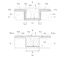
- FIG. 3 is a cross-sectional view showing the dielectric structure of FIG. 2, wherein (a) shows a first dielectric structure and (b) shows a second dielectric structure.
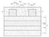
- FIG. 6 is a partial cross-sectional view showing a modification of the semiconductor device of FIG. 2.
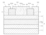
- FIG. 10 is a partial cross-sectional view showing another modification of the semiconductor device of FIG. 2.
- FIG. 1 shows a semiconductor device according to this embodiment, for example, a diode having an AlGaN / GaN heterojunction structure.
- this semiconductor device 1 is a semiconductor device having a lateral structure having comb-shaped electrodes, and is formed on a laminate 2 including a group III-V nitride semiconductor and on the surface of the laminate.
- a comb-shaped Schottky electrode 3 and an ohmic electrode 4 are provided.
- Each of these electrodes 3 and 4 has a plurality of comb teeth extending from the side of each electrode, and by alternately arranging a plurality of comb teeth provided on these electrodes, High density is realized.
- FIG. 2 is a partial cross-sectional view of the semiconductor device 1 taken along line AA in FIG.
- the semiconductor device 1 includes a substrate 11 made of Si, a buffer layer 12 formed on the substrate, a GaN layer 13 (first semiconductor layer) stacked on the buffer layer 12, and a GaN layer 13.
- the semiconductor device 1 is formed so as to integrally cover the opposing surfaces of the Schottky electrode 3 and the ohmic electrode 4 and the surface 14a of the AlGaN layer 14, and is a dielectric structure 5 (first material) made of SiO 2 (first material).
- the Schottky electrode 3 and the ohmic electrode 4 have, for example, a substantially rectangular cross section, and the opposing surfaces of the Schottky electrode 3 and the ohmic electrode 4 constitute inner side surfaces 3a and 4a, respectively.
- the Schottky electrode 3 and the ohmic electrode 4 are made of a highly conductive material.
- the Schottky electrode 3 is, for example, in order from the semiconductor layer side, Ni (100 nm), Au (100 nm), Al or Al alloy (5 to 10 ⁇ m).
- the ohmic electrode 4 is made of, for example, Ti (25 nm), Al (300 nm), Al, or an Al alloy (5 to 10 ⁇ m) in this order from the semiconductor layer side.
- the Schottky electrode 3 and the ohmic electrode 4 are formed with a width of 10 ⁇ m, for example.
- the dielectric structure 5 includes a bottom surface portion 5 a formed on the surface 14 a of the AlGaN layer 14, and a side surface portion 5 b that covers the inner surface 3 a of the Schottky electrode 3.
- the dielectric structure 5 is made of, for example, SiO 2 and has a thickness T1 of, for example, 2.0 ⁇ m.
- the dielectric structure 6 has a layer thickness portion 6a formed on the bottom surface portion 5a and thin layer portions 6b and 6c formed on the top surface portions 5d and 5e. ing.
- the layer thickness portion 6 a is formed so as to be embedded between the Schottky electrode 3 and the ohmic electrode 4.
- the thin layer portions 6b and 6c are formed so as to cover the entire upper surfaces 50d and 50e, respectively.
- the dielectric structure 6 is made of an organic film having a dielectric constant higher than that of SiO 2 , for example, a high dielectric constant polyimide having a dielectric constant of 4.0 or more, and the width D of the layer thickness portion 6a is about 6.0 ⁇ m. It is. By using such a material, the electric field in the organic film can be set to ⁇ 1 / ⁇ 2 ( ⁇ 1 : dielectric constant of SiO 2 , ⁇ 2 : dielectric constant of the organic film). Can be extended.
- the dielectric structures 5 and 6 are used. Since the charges are the same because of the series capacitor, the lower the dielectric constant, the higher the electric field applied. Therefore, by adjusting the thickness of the dielectric structures 5 and 6 between the electrodes, it is possible to realize a long life without generating an excessive voltage in the low breakdown voltage dielectric. Specifically, when the dielectric structure 5 made of the first material is formed with the minimum necessary thickness and the remaining portion is embedded with the second material, an electric field is generated in the dielectric structure 5 having a relatively low dielectric constant. It will take. For this reason, it is possible to prevent dielectric breakdown due to high voltage while preventing cracking due to thickening.
- a two-dimensional electron gas layer is generated by the piezoelectric effect on the GaN layer 13 side of the AlGaN / GaN heterojunction interface.
- the ohmic electrode 4 is electrically connected to the Schottky electrode 3 through the AlGaN / GaN layer on which the two-dimensional electron gas layer 13a having a high carrier concentration is formed.
- the two-dimensional electron gas layer serves as a carrier and the AlGaN / GaN layer has low resistance and high mobility, the on-resistance of the semiconductor device 1 can be reduced and a low on-voltage can be realized. Yes.
- the dielectric structure 5 integrally forms the opposing surfaces of the Schottky electrode and the ohmic electrode and the surface of the second semiconductor layer. And is made of SiO 2 having a predetermined dielectric constant.
- the dielectric structure 6 is made of polyimide which is on the dielectric structure 5 and is formed between the Schottky electrode and the ohmic electrode and has a dielectric constant equal to or higher than that of SiO 2 .
- an SiO 2 layer is formed in the vicinity of each electrode where electric field concentration is likely to occur, and a polyimide layer having a higher dielectric constant than SiO 2 is formed for the remaining part. It is possible to prevent dielectric breakdown that is likely to occur in the vicinity of each electrode, and to prevent cracking of the dielectric structure. Moreover, even if it is difficult to form the entire dielectric structure with only SiO 2 , it can be easily manufactured by using the two materials having the above relationship, and the degree of freedom in design can be improved. it can.
- the dielectric breakdown voltage between the electrodes can be improved, even when the comb-shaped electrodes are arranged at a high density, dielectric breakdown can be prevented from occurring between the electrodes, and a low on-resistance and high breakdown voltage can be prevented. It is possible to manufacture a simple semiconductor device.
- FIG. 4 is a partial cross-sectional view showing a modification of the semiconductor device of FIG.
- the semiconductor device of FIG. 2 has dielectric structures 5 and 6, but the semiconductor device of FIG. 4 is different in that it has an integrally formed dielectric structure 20.
- the semiconductor device of FIG. 2 is demonstrated.
- the dielectric structure 20 is formed so as to integrally cover the opposing surfaces of the Schottky electrode 3 and the ohmic electrode 4 and the surface 14 a of the AlGaN layer 14, and the Schottky electrode 3. Are arranged so as to be buried between the ohmic electrodes 4. That is, the dielectric structure 20 of this modification is obtained by integrally molding the semiconductor structures 5 and 6 of FIG. 2 with SiO 2 .
- the dielectric structure 20 has a layer thickness portion 20a formed on the surface 14a of the AlGaN layer 14 and thin layer portions 20b and 20c formed on the upper surfaces 3b and 4b.
- the dielectric structure needs to be embedded between the Schottky electrode 3 and the ohmic electrode 4. Therefore, the thickness of the dielectric structure depends on the thickness of each electrode formed on the AlGaN layer 14, and in particular, when the thickness of each electrode is increased to about 10 ⁇ m, the thickness of the anode coupling type PECVD is increased. When a normal CVD method is used, the entire dielectric structure may not be formed with only SiO 2 .
- the thickness T2 of the dielectric structure 20 (distance from the surface in contact with the surface 14a of the AlGaN layer 14 to the upper surface) is larger than the thickness (height) of the Schottky electrode 3 or the ohmic electrode 4. Is done.
- the dielectric structure 20 is formed by, for example, a cathode coupling type PECVD method.
- Cathode coupling type PECVD is a type of CVD in which charged particles ionized by plasma are incident on a film to be formed. Since the SiO 2 network is divided by the incident particles, the internal stress is relieved, and as a result, it is presumed that a thick SiO 2 film can be formed as compared with ordinary CVD. Therefore, even when the thickness of each electrode is large, the dielectric structure 20 made of SiO 2 can be formed between the electrodes by adopting the cathode coupling type PECVD method. Further high breakdown voltage can be realized.
- FIG. 5 is a partial cross-sectional view showing a modification of the semiconductor device of FIG.
- the dielectric structure 30 has a layer thickness portion 30a formed on the surface 14a of the AlGaN layer 14, and layer thin portions 30b and 30c formed on the upper surfaces 3b and 4b. Yes.
- the thin layer portion 30b is formed so as to cover a part of the upper surface 3b
- the thin layer portion 30c is formed so as to cover a part of the upper surface 4b. That is, in the dielectric structure 20, the upper surface 3 b of the Schottky electrode 3 and a part of the ohmic electrode 4 are exposed.
- the dielectric structure 30 As described above, by not forming the dielectric structure 30 at a position where no electric field is generated on the upper surface of the electrode, the residual stress of the dielectric structure 30 can be reduced, and cracking of the dielectric structure 30 is surely prevented. can do.
- the invention made by the present inventor has been specifically described based on the embodiment.
- the present invention is not limited to the above embodiment, and can be changed without departing from the gist thereof.
- the electronic device is a diode having a group III nitride semiconductor, but is not limited thereto, and may be a transistor having a group III nitride semiconductor.
- the present invention can be applied to an insulating film between a source electrode and a drain electrode. Further, it may be an SOI diode or an SOI transistor.
- an ohmic electrode drain electrode
- a Schottky electrode gate electrode
- the SiO 2 which is an interlayer insulating film formed by plasma CVD method or a thermal CVD method, and opening the SiO 2 by etching the necessary portion of the ohmic electrode and the Schottky electrode by photolithography and hydrofluoric acid.
- pure Al or Al alloy AlSi, AlCu, etc.
- AlSi, AlCu, etc. pure Al or Al alloy
- polyimide dielectric constant 4.0
- the coating thickness was applied under the condition that the bare silicon substrate on which no pattern was formed was 20 ⁇ m so that polyimide was also formed on the upper surface of the electrode. Thereafter, a resist was applied and the polyimide was patterned, followed by curing at 380 ° C.
- Example 2 instead of the polyimide of Example 1, an organic film having a dielectric constant higher than that of polyimide was used.
- the dielectric constant of SiO 2 was 3.9 and the dielectric constant between the organic films was X, the charge was 3.9 / X times, so a lower voltage was applied to the organic film than in the case of polyimide.
- Example 3 It was produced in the same manner as in Example 1 until the aluminum wiring was formed.
- a SiO 2 film having a thickness of 5000 nm was formed by cathode-coupled PECVD.
- the raw materials at that time were TEOS and oxygen.
- the pad portion was opened with buffered hydrofluoric acid containing ethylene glycol.
- polyimide was applied.
- the coating thickness was applied on a bare silicon substrate on which no pattern was formed under the condition of 20 ⁇ m.
- a resist was applied and the polyimide was patterned, followed by curing at 380 ° C.
Landscapes
- Electrodes Of Semiconductors (AREA)
- Junction Field-Effect Transistors (AREA)
- Internal Circuitry In Semiconductor Integrated Circuit Devices (AREA)
- Formation Of Insulating Films (AREA)
Abstract
横型構造の半導体デバイスにおいて、電極間に高電界が生じる場合であっても信頼性を向上することができる半導体デバイスを提供する。 半導体デバイス1は、Siからなる基板11と、該基板上に形成されたバッファ層12と、バッフャ層12上に積層されたGaN層13と、GaN層13上に積層され、GaNとヘテロ接合された他のGaN系化合物を含むAlGaN層14と、AlGaN層14の表面14aに所定間隔で形成されたショットキー電極3およびオーミック電極4とを備えている。また半導体デバイス1は、電極3,4のそれぞれの対向面3a,4aとAlGaN層14の表面14aとを一体的に覆って形成され、SiO2からなる誘電体構造5と、誘電体構造5上であり且つ電極3,4の間に、SiO2と同じかそれ以上の誘電率を有する材料からなる誘電体構造6とを備えている。
Description
本発明は、パワーエレクトロニクス用デバイス等に用いられるIII-V族窒化物系化合物半導体を有する半導体デバイスおよびその製造方法に関する。
III族窒化物半導体は、およそ3.3MV/cmの高い絶縁破壊電界を有しており、従来のSiデバイスに比べて小さいチップ面積で同じ性能のパワー半導体装置が作製できると考えられている。しかし、III族窒化物半導体は、サファイヤなどの絶縁基板上やSi基板等の導電基板を使用しても、基板上のバッファ層内にAlNを使用することで高抵抗化していることから、横型素子が主流である。そのため、ダイオードやトランジスタを作製する場合、高電圧が印加される電極が同一平面に存在することになる。特に、素子の高密度化を図った場合、各電極が櫛歯型電極構造となり、電圧差が600Vのソース電極とドレイン電極が10μm程度の間隔で、交互に同一平面に配置されることになる。特に、配線抵抗を低減するためには配線幅を広げる必要があることから、配線としてのソース電極とドレイン電極の双方の幅が広げられ、これら電極間の距離が数μmまで縮小される。このため、電極間電界は平均電界で数MV/cmに達し、局所的には更に高くなる。
従来、Siデバイスでは電極間にポリイミドを充填していた。これは、Siの絶縁破壊電界が0.3MV/cmであるのに対し、ポリイミドは4~5MV/cmであり、絶縁破壊電界に10倍程度の差があることによる。しかし、GaNの絶縁破壊電界は3.3MV/cmであり、ポリイミドと同程度であることから、平均電界では問題ないが、電極の角隅部など電界集中点においては、ポリイミドの絶縁破壊電界を超す可能性がある。
さらに配線抵抗を下げるために配線幅を広げ、配線間距離が狭くなると、ポリイミドの絶縁破壊電界を超える可能性がある。そのため、従来のように電極間を単にポリイミドで充填していたのでは、ポリイミドが絶縁破壊を起こす問題があった。
例えば、配線間の絶縁膜の耐圧が空気より高く、GaNより低くなっている誘電体構造が提案されている(特許文献1)。しかしながら、本構成では、GaNより先に絶縁膜が降伏してしまい、高耐圧素子を作製することはできない。
また、横型IGBT(Insulated Gate Bipolar Transistor)において、エミッタ電極が、素子上部を層間絶縁膜を介して覆っている誘電体構造が提案されている(特許文献2)。本構成では、必然的にコレクタ電極の上面が覆われることになる。このような構造の場合、コレクタ電極とエミッタ電極から延びた電極との間の層間絶縁膜の耐圧が問題になると思われるが、Siの絶縁破壊耐圧が低い為、それ依然に、コレクタ電極周辺の電界集中が問題になると考えられる。このため、コレクタ電極近傍に半導体層に食い込む形状の絶縁層を設けて、電界集中を防いでいる。このように、絶縁層がSiの場合には、Siの絶縁破壊耐圧が低い為、層間絶縁膜の耐圧は問題にならないと考えられる。
また、他の横型IGBTは、高電圧のかかるコレクタ電極とエミッタ電極が交差している構造を有している(特許文献3)。この横型IGBTでは、特許文献2の構成と同様、半導体部の電界集中について考慮しているものの、層間絶縁膜自体については考慮していない。
特許文献4では、HV IC(High Voltage Integrated Circuit)の一例として、Siデバイスにおいて高圧部の周辺を低圧部が覆うようにして、かつその間を高耐圧MOSFETで繋ぎ、その構造を工夫することで層間絶縁膜に高い電界が生じるようにしている。これはSiデバイスが横型構造のみならず縦型構造を採用することができ、縦方向で耐圧を持たせることが可能となっている。また、層間絶縁膜に高い電界が発生する構成では(図17参照)、GaNのデバイスのように対向する電極間で電界が生じる訳ではなく、層間絶縁膜での電界強度はGaNに比べて低いと考えられる。このように、SiのHV IC等においても、横型の対向する配線間の耐圧を考慮する必要が無いと考えられる。また、この特許文献4におけるトレンチ分離部の作製方法では(図4参照)、トレンチをエッチングして熱酸化しているが、本方法はSiであるが故に実行できるのであり、GaNで実行するのは本質的に困難である。
本発明の目的は、横型構造の半導体デバイスにおいて、電極間に高電界が生じる場合であっても信頼性を向上することができる半導体デバイスおよびその製造方法を提供することにある。
上記目的を達成するために、本発明に係る半導体デバイスは、横型構造の半導体デバイスであって、基板と、前記基板上に積層され、GaN系化合物を含む第1半導体層と、前記第1半導体層上に積層され、前記GaN系化合物とヘテロ接合された他のGaN系化合物を含む第2半導体層と、前記第2半導体層の表面に所定間隔で形成された第1電極および第2電極と、前記第1電極および前記第2電極のそれぞれの対向面と、前記第2半導体層の表面とを一体的に覆って形成され、所定の誘電率を有する第1材料からなる第1誘電体構造と、前記第1誘電体構造上であり且つ前記第1電極および第2電極の間に形成され、前記第1材料と同じかそれ以上の誘電率を有する第2材料からなる第2誘電体構造と、を備えることを特徴とする半導体デバイス。
前記第1材料はSiO2であるのが好ましく、また、前記第2材料は、ポリイミドと同じかそれ以上の誘電率を有する材料であるのが好ましい。
また、前記第2材料がSiO2であるのが好ましい。
また、前記第1電極および前記第2電極が櫛歯型電極構造を形成してもよい。
さらに、前記1誘電体構造が、前記第1電極の上面の少なくとも一部と、前記第2電極の上面の少なくとも一部とを覆って形成されてもよい。
また、前記第1誘電体構造が、前記第1電極の上面および前記第2電極の上面の全面を覆って形成されてもよい。
また、前記半導体デバイスがダイオードまたはトランジスタで構成されてもよい。
本発明に係る半導体デバイスの製造方法は、横型構造の半導体デバイスの製造方法であって、基板上に、GaN系化合物を含む第1半導体層を形成するステップと、前記第1半導体層上に、前記GaN系化合物とヘテロ接合された他のGaN系化合物を含む第2半導体層を形成するステップと、前記第2半導体層の表面に、第1電極および第2電極を所定の間隔で形成するステップと、前記第1電極および前記第2電極のそれぞれの対向面と、前記第2半導体層の表面とを一体的に覆う第1誘電体構造を、所定の誘電率を有する第1材料で形成するステップと、前記第1誘電体構造上であり且つ前記第1電極と前記第2電極との間に、前記第1材料と同じかそれ以上の誘電率を有する材料で第2誘電体構造を形成するステップと、を備えることを特徴とする。
また、前記第1材料および前記第2材料がSiO2であり、前記第2誘電体構造は、カソードカップリング型PECVD法にて、前記第1誘電体構造と一体的に成形されるのが好ましい。
また、前記第1誘電体構造が、前記第1電極の上面の少なくとも一部と、前記第2電極の上面の少なくとも一部とを覆って形成されてもよい。
本発明によれば、横型構造の半導体デバイスにおいて、第1誘電体構造が、第1電極および第2電極のそれぞれの対向面と、第2半導体層の表面とを一体的に覆って形成され、かつ、所定の誘電率を有する第1材料からなる。また、第2誘電体構造が、第1誘電体構造上であり且つ第1電極および第2電極の間に形成され、かつ、第1材料と同じかそれ以上の誘電率を有する第2材料からなる。すなわち、第1電極と第2電極の間で、電界集中の生じ易い各電極の近傍には第1材料の層が形成され、残りの部分については第1材料と誘電率が同じ、またはより誘電率の高い第2材料の層が形成されるので、各電極の近傍で生じ易い絶縁破壊を防止することができ、加えて誘電体構造の割れを防止することができる。したがって、電極間に高電界が生じる場合であっても信頼性を向上することができる。
また、第1誘電体構造をSiO2で形成し、第2誘電体構造をSiO2より誘電率の高いポリイミドで形成することで、誘電率は低いが絶縁破壊耐圧の高いSiO2と、誘電率が高く、割れを生じにくいポリイミドとで電極間が埋め込まれる。したがって、各電極の近傍で生じ易い絶縁破壊を防止できると共に、割れ等が生じない信頼性の高い誘電体構造を作製することができる。
以下、本発明の実施の形態を図面を参照しながら詳細に説明する。
図1は、本実施形態に係る半導体デバイスで、例えば、AlGaN/GaNのヘテロ接合構造を有するダイオードである。この半導体デバイス1は、図1に示すように、櫛歯型電極を有する横型構造の半導体デバイスであって、III-V族窒化物半導体を含む積層体2と、積層体の表面に形成された櫛歯型のショットキー電極3およびオーミック電極4とを備えている。これらの電極3,4は、各電極の側方から延出する複数の櫛歯部をそれぞれ有しており、これら電極に設けられた複数の櫛歯部を交互に配置することで、素子の高密度化を実現している。
図2は、図1の線A-Aに沿う半導体デバイス1の部分断面図である。
半導体デバイス1は、Siからなる基板11と、該基板上に形成されたバッファ層12と、バッファ層12上に積層されたGaN層13(第1半導体層)と、GaN層13上に積層され、GaNとヘテロ接合された他のGaN系化合物を含むAlGaN層14(第2半導体層)と、AlGaN層14の表面14aに所定間隔で形成されたショットキー電極3(第1電極)およびオーミック電極4(第2電極)とを備えている。また半導体デバイス1は、ショットキー電極3およびオーミック電極4のそれぞれの対向面とAlGaN層14の表面14aとを一体的に覆って形成され、SiO2(第1材料)からなる誘電体構造5(第1誘電体構造)と、誘電体構造5上であり且つショットキー電極3およびオーミック電極4の間に、SiO2と同じかそれ以上の誘電率を有する材料(第2材料)からなる誘電体構造6(第2誘電体構造)とを備えている。
ショットキー電極3およびオーミック電極4は、例えば断面略矩形であり、ショットキー電極3とオーミック電極4の対向面が、それぞれ内側面3a,4aを構成している。これらショットキー電極3およびオーミック電極4は、高導電性の材料からなり、ショットキー電極3は例えば、半導体層側から順に、Ni(100nm)、Au(100nm)、AlもしくはAl合金(5~10μm)からなり、オーミック電極4は例えば、半導体層側から順に、Ti(25nm)、Al(300nm)、AlもしくはAl合金(5~10μm)からなる。また、このショットキー電極3およびオーミック電極4は、例えば幅10μmで形成される。
誘電体構造5は、具体的には、図3(a)に示すように、AlGaN層14の表面14aに形成された底面部5aと、ショットキー電極3の内側面3aを覆う側面部5bと、ショットキー電極3の上面3bを覆う上面部5dと、オーミック電極4の内側面4aを覆う側面部5cと、オーミック電極4の上面4bを覆う上面部5eとを有している。この誘電体構造5は、例えばSiO2からなり、その厚さT1が、例えば2.0μmとなるように形成されている。
誘電体構造6は、図3(b)に示すように、底面部5a上に形成された層厚部6aと、上面部5d,5e上に形成された層薄部6b,6cとを有している。層厚部6aは、ショットキー電極3およびオーミック電極4の間に埋設するように形成されている。また、層薄部6b,6cは、それぞれ上面50d,50eの全体を覆って形成されている。この誘電体構造6は、具体的には、SiO2より誘電率の高い有機膜、例えば誘電率が4.0以上の高誘電率ポリイミドからなり、層厚部6aの幅Dは約6.0μmである。このような材料を用いることによって、有機膜中の電界をε1/ε2(ε1:SiO2の誘電率、ε2:有機膜の誘電率)にすることができるため、有機膜の寿命を延ばすことが可能となる。
また、本実施形態において、誘電体構造5を形成する材料を第1材料、誘電体構造6を形成する材料を、第1材料より耐圧の大きい第2材料としたとき、誘電体構造5,6は直列コンデンサの関係より、その電荷が同じになるため、誘電率の低いもの程、高電界がかかる。よって、電極間における誘電体構造5,6の厚さを調整することで、低耐圧な誘電体に過剰な電圧が生じず、長寿命を実現することも可能である。具体的には、第1材料からなる誘電体構造5を必要最低限の厚さで形成し、残りの部分を第2材料で埋め込むと、相対的に誘電率の低い誘電体構造5に電界がかかることになる。このため、厚膜化による割れを防止しつつ、高電圧による絶縁破壊を防止することができる。
上記のようなAlGaN/GaNヘテロ接合構造を有する半導体デバイス1では、AlGaN/GaNヘテロ接合界面のGaN層13側に、ピエゾ効果によって2次元電子ガス層が発生している。そして、高キャリア濃度の2次元電子ガス層13aが形成されたAlGaN/GaN層を介して、オーミック電極4がショットキー電極3と電気的に接続される。このとき、2次元電子ガス層がキャリアとなってAlGaN/GaN層が低抵抗、高移動度となるため、半導体デバイス1のオン抵抗を小さくし、低オン電圧を実現することが可能となっている。
本実施形態によれば、櫛歯型電極を有する横型構造の半導体デバイス1において、誘電体構造5が、ショットキー電極およびオーミック電極のそれぞれの対向面と、第2半導体層の表面とを一体的に覆って形成され、かつ、所定の誘電率を有するSiO2からなる。また、誘電体構造6が、誘電体構造5上であり且つショットキー電極およびオーミック電極の間に形成され、かつ、SiO2と同じかそれ以上の誘電率を有するポリイミドからなる。すなわち、ショットキー電極とオーミック電極の間で、電界集中の生じ易い各電極の近傍にはSiO2層が形成され、残りの部分についてはSiO2より誘電率の高いポリイミド層が形成されるので、各電極の近傍で生じ易い絶縁破壊を防止することができ、加えて誘電体構造の割れを防止することができる。また、SiO2のみでは誘電体構造全体を形成し難い場合であっても、上記関係を有する2つの材料を使用することで容易に作製することが可能となり、設計の自由度を向上させることができる。
さらに、電極間の絶縁破壊耐圧を向上することができるため、櫛歯型電極を高密度に配置した場合でも、電極間で絶縁破壊が生じるのを防止することができ、低オン抵抗で高耐圧な半導体デバイスを作製することが可能となる。
図4は、図2の半導体デバイスの変形例を示す部分断面図である。図2の半導体デバイスは誘電体構造5,6を有しているが、図4の半導体デバイスは、一体成形された誘電体構造20を有している点で異なる。以下、図2の半導体デバイスと異なる部分を説明する。
図4の半導体デバイスにおいて、誘電体構造20は、ショットキー電極3およびオーミック電極4のそれぞれの対向面と、AlGaN層14の表面14aとを一体的に覆って形成され、かつ、ショットキー電極3とオーミック電極4の間に埋設するように配置されている。すなわち、本変形例の誘電体構造20は、図2の半導体構造5,6をSiO2にて一体的に成形したものである。この誘電体構造20は、AlGaN層14の表面14a上に形成された層厚部20aと、上面3b,4b上に形成された層薄部20b,20cとを有している。
ここで、誘電体構造はショットキー電極3とオーミック電極4との間に埋め込んで形成する必要がある。したがって、誘電体構造の厚さはAlGaN層14上に形成される各電極の厚さに依存することとなり、とりわけ、各電極の厚さが10μm程度まで大きくなると、アノードカップリング型PECVDのような通常のCVD法を用いた場合にSiO2のみでは誘電体構造全体を形成できない場合がある。
本実施形態では、誘電体構造20の厚さT2(AlGaN層14の表面14aと接する面から上面までの距離)が、ショットキー電極3あるいはオーミック電極4の厚さ(高さ)よりも大きく形成される。このとき、誘電体構造20は、例えばカソードカップリング型PECVD法にて形成される。カソードカップリング型PECVDとは、成膜される膜にプラズマでイオン化された荷電粒子が入射してくるタイプのCVDである。入射する粒子により、SiO2のネットワークが分断されるので内部応力が緩和され、その結果通常のCVDと比較して厚いSiO2が成膜できると推察される。したがって、各電極の厚さが大きい場合であっても、カソードカップリング型PECVD法を採用することにより、電極間にSiO2からなる誘電体構造20を形成することができ、誘電体構造20の更なる高耐圧を実現することができる。
図5は、図4の半導体デバイスの変形例を示す部分断面図である。
図5に示すように、誘電体構造30は、AlGaN層14の表面14a上に形成された層厚部30aと、上面3b,4b上に形成された層薄部30b,30cとを有している。そして、層薄部30bは上面3bの一部を覆って形成され、層薄部30cは上面4bの一部を覆って形成されている。すなわち、誘電体構造20では、ショットキー電極3の上面3bとオーミック電極4の一部が露出している。
このように、電極の上面において、電界が生じない位置には誘電体構造30を形成しないことにより、誘電体構造30の残留応力を減少させることができ、誘電体構造30の割れを確実に防止することができる。
以上、本発明者によってなされた発明を実施形態に基づいて具体的に説明したが、本発明は上記実施形態に限定されるものではなく、その要旨を逸脱しない範囲で変更可能である。
例えば、本実施形態では電子デバイスはIII族窒化物半導体を有するダイオードであるが、これに限らず、III族窒化物半導体を有するトランジスタであってもよい。トランジスタの場合はソース電極とドレイン電極間の絶縁膜について本願発明を適用できる。また、SOIダイオードまたはSOIトランジスタであってもよい。
以下、本発明の実施例を説明する。
(実施例1)
先ず、基板としてSi(111)を準備し、この基板をMOCVD装置内に導入して結晶成長を行う。具体的には、AlN層100nmを成長後、AlN/GaN=20/200nmを12回繰り返してバッファ層を成長させた。次に、炭素濃度が1×1019cm-3以上の高抵抗GaN層を1000nm成長させ、その後、炭素濃度が1×1017cm-3以下の低抵抗GaN層を100nm成長させた。次いで、Al組成25%のAlGaN層を25nm成長させ、ヘテロ接合界面を形成した。
先ず、基板としてSi(111)を準備し、この基板をMOCVD装置内に導入して結晶成長を行う。具体的には、AlN層100nmを成長後、AlN/GaN=20/200nmを12回繰り返してバッファ層を成長させた。次に、炭素濃度が1×1019cm-3以上の高抵抗GaN層を1000nm成長させ、その後、炭素濃度が1×1017cm-3以下の低抵抗GaN層を100nm成長させた。次いで、Al組成25%のAlGaN層を25nm成長させ、ヘテロ接合界面を形成した。
その後、オーミック電極(ドレイン電極)とショットキー電極(ゲート電極)とを、フォトリソグラフィーとスパッタリング、リフトオフ、アニール等の工程を経て形成した。
その後、層間絶縁膜であるSiO2をプラズマCVD法や熱CVD法により形成し、オーミック電極とショットキー電極の必要部をフォトリソグラフィーとフッ酸によるエッチングによりSiO2を開口した。
次に、純AlやAl合金(AlSi、AlCu等)を10μm成膜させ、その後、フォトリソグラフィーと塩素系ドライエッチングによりアルミをエッチングして、アルミ配線をパターンニングした。
次いで、アノードカップリング型PECVDを用いてSiO2を2μm成膜したのち、ポリイミド(誘電率4.0)を塗布した。塗布厚は電極上面にもポリイミドが形成されるように、パターンを形成していないベアシリコン基板で20μmとなるような条件で塗布した。その後、レジストを塗って、ポリイミドをパターンニングした後、380℃でキュアを行った。
(実施例2)
実施例1のポリイミドに代えて、ポリイミドより誘電率の高い有機膜を使用した。SiO2の誘電率が3.9であり、有機膜間の誘電率がXの場合、電荷は3.9/X倍となることから、ポリイミドの場合よりも低い電圧が有機膜にかかった。
実施例1のポリイミドに代えて、ポリイミドより誘電率の高い有機膜を使用した。SiO2の誘電率が3.9であり、有機膜間の誘電率がXの場合、電荷は3.9/X倍となることから、ポリイミドの場合よりも低い電圧が有機膜にかかった。
(実施例3)
アルミ配線を形成するまでは、実施例1と同様に作製した。
アルミ配線を形成するまでは、実施例1と同様に作製した。
その後、カソードカップル型PECVDでSiO2を5000nm成膜した。そのときの原料はTEOSと酸素であった。その後、パット部分をエチレングリコール含有の緩衝フッ酸で開口した。
(比較例)
アルミ配線を形成するまでは、実施例1と同様に作製した。
アルミ配線を形成するまでは、実施例1と同様に作製した。
その後、ポリイミドを塗布した。塗布厚はパターンを形成していないベアシリコン基板で20μmとなるような条件で塗布した。その後、レジストを塗って、ポリイミドをパターンニングした後、380℃でキュアを行った。
上記のように作製した半導体デバイスの耐圧性を検証した結果、実施例1~3の場合、電極間に高電圧が生じる場合であっても、電極間での絶縁破壊を防止することができ、高耐圧な半導体デバイスを作製できることが分かった。
1 半導体デバイス
2 積層体
3 ショットキー電極
3a,4a 対向面
3b,4b 上面
4 オーミック電極
5a 底面部
5b 側面部
5c 側面部
5d 上面部
5e 上面部
6a 層厚部
6b,6c 層薄部
11 基板
12 バッファ層
13 GaN層
13a 2次元電子ガス層
14 AlGaN層
14a 表面
5 誘電体構造
6 誘電体構造
20 誘電体構造
20a 層厚部
20b,20c 層薄部
30 誘電体構造
30a 層厚部
30b,30c 層薄部
50d,50e 上面
2 積層体
3 ショットキー電極
3a,4a 対向面
3b,4b 上面
4 オーミック電極
5a 底面部
5b 側面部
5c 側面部
5d 上面部
5e 上面部
6a 層厚部
6b,6c 層薄部
11 基板
12 バッファ層
13 GaN層
13a 2次元電子ガス層
14 AlGaN層
14a 表面
5 誘電体構造
6 誘電体構造
20 誘電体構造
20a 層厚部
20b,20c 層薄部
30 誘電体構造
30a 層厚部
30b,30c 層薄部
50d,50e 上面
Claims (11)
- 横型構造の半導体デバイスであって、
基板と、
前記基板上に積層され、GaN系化合物を含む第1半導体層と、
前記第1半導体層上に積層され、前記GaN系化合物とヘテロ接合された他のGaN系化合物を含む第2半導体層と、
前記第2半導体層の表面に所定間隔で形成された第1電極および第2電極と、
前記第1電極および前記第2電極のそれぞれの対向面と、前記第2半導体層の表面とを一体的に覆って形成され、所定の誘電率を有する第1材料からなる第1誘電体構造と、
前記第1誘電体構造上であり且つ前記第1電極および第2電極の間に形成され、前記第1材料と同じかそれ以上の誘電率を有する第2材料からなる第2誘電体構造と、
を備えることを特徴とする半導体デバイス。 - 前記第1材料はSiO2であることを特徴とする請求項1記載の半導体デバイス。
- 前記第2材料は、ポリイミドと同じかそれ以上の誘電率を有する材料であることを特徴とする、請求項1記載の半導体デバイス。
- 前記第2材料がSiO2であることを特徴とする請求項1記載の半導体デバイス。
- 前記第1電極および前記第2電極が櫛歯型電極構造を形成することを特徴とする請求項1乃至4のいずれか1項に記載の半導体デバイス。
- 前記第1誘電体構造が、前記第1電極の上面の少なくとも一部と、前記第2電極の上面の少なくとも一部とを覆って形成されることを特徴とする、請求項1乃至5のいずれか1項に記載の半導体デバイス。
- 前記第1誘電体構造が、前記第1電極の上面および前記第2電極の上面の全面を覆って形成されることを特徴とする、請求項1乃至6のいずれか1項に記載の半導体デバイス。
- 前記半導体デバイスが、ダイオードまたはトランジスタで構成されることを特徴とする、請求項1乃至7のいずれか1項に記載の半導体デバイス。
- 横型構造の半導体デバイスの製造方法であって、
基板上に、GaN系化合物を含む第1半導体層を形成するステップと、
前記第1半導体層上に、前記GaN系化合物とヘテロ接合された他のGaN系化合物を含む第2半導体層を形成するステップと、
前記第2半導体層の表面に、第1電極および第2電極を所定の間隔で形成するステップと、
前記第1電極および前記第2電極のそれぞれの対向面と、前記第2半導体層の表面とを一体的に覆う第1誘電体構造を、所定の誘電率を有する第1材料で形成するステップと、
前記第1誘電体構造上であり且つ前記第1電極と前記第2電極との間に、前記第1材料と同じかそれ以上の誘電率を有する材料で第2誘電体構造を形成するステップと、
を備えることを特徴とする半導体デバイスの製造方法。 - 前記第1材料および前記第2材料がSiO2であり、
前記第2誘電体構造は、カソードカップリング型PECVD法にて、前記第1誘電体構造と一体的に成形されることを特徴とする、請求項9記載の製造方法。 - 前記第1誘電体構造が、前記第1電極の上面の少なくとも一部と、前記第2電極の上面の少なくとも一部とを覆って形成されることを特徴とする、請求項9または10に記載の製造方法。
Applications Claiming Priority (2)
| Application Number | Priority Date | Filing Date | Title |
|---|---|---|---|
| JP2012147328A JP2014011329A (ja) | 2012-06-29 | 2012-06-29 | 半導体デバイスおよびその製造方法 |
| JP2012-147328 | 2012-06-29 |
Publications (1)
| Publication Number | Publication Date |
|---|---|
| WO2014002672A1 true WO2014002672A1 (ja) | 2014-01-03 |
Family
ID=49782839
Family Applications (1)
| Application Number | Title | Priority Date | Filing Date |
|---|---|---|---|
| PCT/JP2013/064851 Ceased WO2014002672A1 (ja) | 2012-06-29 | 2013-05-29 | 半導体デバイスおよびその製造方法 |
Country Status (2)
| Country | Link |
|---|---|
| JP (1) | JP2014011329A (ja) |
| WO (1) | WO2014002672A1 (ja) |
Families Citing this family (3)
| Publication number | Priority date | Publication date | Assignee | Title |
|---|---|---|---|---|
| JP6884026B2 (ja) * | 2017-04-19 | 2021-06-09 | 三井化学株式会社 | 半導体用膜形成用組成物、半導体用膜形成用組成物の製造方法、半導体用部材の製造方法、及び半導体用工程材の製造方法 |
| JP7095615B2 (ja) * | 2019-02-12 | 2022-07-05 | 株式会社デンソー | 半導体装置 |
| US11842937B2 (en) * | 2021-07-30 | 2023-12-12 | Wolfspeed, Inc. | Encapsulation stack for improved humidity performance and related fabrication methods |
Citations (6)
| Publication number | Priority date | Publication date | Assignee | Title |
|---|---|---|---|---|
| JP2000003919A (ja) * | 1998-06-16 | 2000-01-07 | Nec Corp | 電界効果型トランジスタ |
| WO2007040160A1 (ja) * | 2005-09-30 | 2007-04-12 | Nec Corporation | 電界効果トランジスタ |
| JP2008218696A (ja) * | 2007-03-05 | 2008-09-18 | Nec Corp | 電界効果トランジスタ |
| JP2010199321A (ja) * | 2009-02-25 | 2010-09-09 | Fujitsu Ltd | 化合物半導体装置及びその製造方法 |
| JP2011210750A (ja) * | 2010-03-26 | 2011-10-20 | Nec Corp | 電界効果トランジスタ、電界効果トランジスタの製造方法、および電子装置 |
| JP2011228719A (ja) * | 2011-05-23 | 2011-11-10 | Renesas Electronics Corp | Dc/dcコンバータ用半導体装置 |
Family Cites Families (1)
| Publication number | Priority date | Publication date | Assignee | Title |
|---|---|---|---|---|
| AU2399200A (en) * | 1999-01-08 | 2000-07-24 | Origin Medsystems, Inc. | Combined vessel dissection and transection device and method |
-
2012
- 2012-06-29 JP JP2012147328A patent/JP2014011329A/ja active Pending
-
2013
- 2013-05-29 WO PCT/JP2013/064851 patent/WO2014002672A1/ja not_active Ceased
Patent Citations (6)
| Publication number | Priority date | Publication date | Assignee | Title |
|---|---|---|---|---|
| JP2000003919A (ja) * | 1998-06-16 | 2000-01-07 | Nec Corp | 電界効果型トランジスタ |
| WO2007040160A1 (ja) * | 2005-09-30 | 2007-04-12 | Nec Corporation | 電界効果トランジスタ |
| JP2008218696A (ja) * | 2007-03-05 | 2008-09-18 | Nec Corp | 電界効果トランジスタ |
| JP2010199321A (ja) * | 2009-02-25 | 2010-09-09 | Fujitsu Ltd | 化合物半導体装置及びその製造方法 |
| JP2011210750A (ja) * | 2010-03-26 | 2011-10-20 | Nec Corp | 電界効果トランジスタ、電界効果トランジスタの製造方法、および電子装置 |
| JP2011228719A (ja) * | 2011-05-23 | 2011-11-10 | Renesas Electronics Corp | Dc/dcコンバータ用半導体装置 |
Also Published As
| Publication number | Publication date |
|---|---|
| JP2014011329A (ja) | 2014-01-20 |
Similar Documents
| Publication | Publication Date | Title |
|---|---|---|
| US8829568B2 (en) | Gallium nitride semiconductor device and method for producing the same | |
| JP5649347B2 (ja) | 半導体装置 | |
| JP5776217B2 (ja) | 化合物半導体装置 | |
| JP4737471B2 (ja) | 半導体装置およびその製造方法 | |
| CN102005474B (zh) | 半导体装置及其制造方法 | |
| JP5348364B2 (ja) | ヘテロ接合型電界効果半導体装置 | |
| JP4810072B2 (ja) | 窒素化合物含有半導体装置 | |
| CN103325828B (zh) | 氮化物半导体元件 | |
| JP5470705B2 (ja) | 半導体装置及びその製造方法 | |
| JP5789967B2 (ja) | 半導体装置及びその製造方法、電源装置 | |
| JP2012109492A (ja) | 化合物半導体装置 | |
| JP2007242853A (ja) | 半導体基体及びこれを使用した半導体装置 | |
| JP6496149B2 (ja) | 半導体装置および半導体装置の製造方法 | |
| WO2012160757A1 (ja) | ショットキーダイオード | |
| JP7258124B2 (ja) | 半導体装置および半導体モジュール | |
| WO2013137267A1 (ja) | 窒化物系化合物半導体素子 | |
| CN103681858A (zh) | 半导体装置 | |
| JP2017054960A (ja) | 半導体装置 | |
| JP2009522812A (ja) | 電界緩和機能を有するiii族窒化物電力半導体 | |
| JP2017174937A (ja) | 半導体装置 | |
| WO2014002672A1 (ja) | 半導体デバイスおよびその製造方法 | |
| CN103314438A (zh) | 氮化物系半导体装置 | |
| WO2015129131A1 (ja) | 半導体装置 | |
| JP2020194919A (ja) | 半導体装置 | |
| JP2011142182A (ja) | 電界効果トランジスタ |
Legal Events
| Date | Code | Title | Description |
|---|---|---|---|
| 121 | Ep: the epo has been informed by wipo that ep was designated in this application |
Ref document number: 13809550 Country of ref document: EP Kind code of ref document: A1 |
|
| NENP | Non-entry into the national phase |
Ref country code: DE |
|
| 122 | Ep: pct application non-entry in european phase |
Ref document number: 13809550 Country of ref document: EP Kind code of ref document: A1 |