WO2014002592A1 - Structure pour apposer un câble sur un panneau de câblage, câble, et procédé de fabrication de câble - Google Patents
Structure pour apposer un câble sur un panneau de câblage, câble, et procédé de fabrication de câble Download PDFInfo
- Publication number
- WO2014002592A1 WO2014002592A1 PCT/JP2013/061839 JP2013061839W WO2014002592A1 WO 2014002592 A1 WO2014002592 A1 WO 2014002592A1 JP 2013061839 W JP2013061839 W JP 2013061839W WO 2014002592 A1 WO2014002592 A1 WO 2014002592A1
- Authority
- WO
- WIPO (PCT)
- Prior art keywords
- conductor
- hole
- cable
- ground
- columnar
- Prior art date
Links
Images


Classifications
-
- H—ELECTRICITY
- H01—ELECTRIC ELEMENTS
- H01R—ELECTRICALLY-CONDUCTIVE CONNECTIONS; STRUCTURAL ASSOCIATIONS OF A PLURALITY OF MUTUALLY-INSULATED ELECTRICAL CONNECTING ELEMENTS; COUPLING DEVICES; CURRENT COLLECTORS
- H01R12/00—Structural associations of a plurality of mutually-insulated electrical connecting elements, specially adapted for printed circuits, e.g. printed circuit boards [PCB], flat or ribbon cables, or like generally planar structures, e.g. terminal strips, terminal blocks; Coupling devices specially adapted for printed circuits, flat or ribbon cables, or like generally planar structures; Terminals specially adapted for contact with, or insertion into, printed circuits, flat or ribbon cables, or like generally planar structures
- H01R12/50—Fixed connections
- H01R12/59—Fixed connections for flexible printed circuits, flat or ribbon cables or like structures
- H01R12/62—Fixed connections for flexible printed circuits, flat or ribbon cables or like structures connecting to rigid printed circuits or like structures
-
- H—ELECTRICITY
- H01—ELECTRIC ELEMENTS
- H01P—WAVEGUIDES; RESONATORS, LINES, OR OTHER DEVICES OF THE WAVEGUIDE TYPE
- H01P1/00—Auxiliary devices
- H01P1/04—Fixed joints
- H01P1/047—Strip line joints
-
- H—ELECTRICITY
- H01—ELECTRIC ELEMENTS
- H01P—WAVEGUIDES; RESONATORS, LINES, OR OTHER DEVICES OF THE WAVEGUIDE TYPE
- H01P3/00—Waveguides; Transmission lines of the waveguide type
- H01P3/02—Waveguides; Transmission lines of the waveguide type with two longitudinal conductors
- H01P3/08—Microstrips; Strip lines
- H01P3/085—Triplate lines
-
- H—ELECTRICITY
- H01—ELECTRIC ELEMENTS
- H01P—WAVEGUIDES; RESONATORS, LINES, OR OTHER DEVICES OF THE WAVEGUIDE TYPE
- H01P5/00—Coupling devices of the waveguide type
- H01P5/08—Coupling devices of the waveguide type for linking dissimilar lines or devices
- H01P5/085—Coaxial-line/strip-line transitions
-
- H—ELECTRICITY
- H01—ELECTRIC ELEMENTS
- H01R—ELECTRICALLY-CONDUCTIVE CONNECTIONS; STRUCTURAL ASSOCIATIONS OF A PLURALITY OF MUTUALLY-INSULATED ELECTRICAL CONNECTING ELEMENTS; COUPLING DEVICES; CURRENT COLLECTORS
- H01R12/00—Structural associations of a plurality of mutually-insulated electrical connecting elements, specially adapted for printed circuits, e.g. printed circuit boards [PCB], flat or ribbon cables, or like generally planar structures, e.g. terminal strips, terminal blocks; Coupling devices specially adapted for printed circuits, flat or ribbon cables, or like generally planar structures; Terminals specially adapted for contact with, or insertion into, printed circuits, flat or ribbon cables, or like generally planar structures
- H01R12/50—Fixed connections
- H01R12/51—Fixed connections for rigid printed circuits or like structures
- H01R12/53—Fixed connections for rigid printed circuits or like structures connecting to cables except for flat or ribbon cables
-
- H—ELECTRICITY
- H01—ELECTRIC ELEMENTS
- H01R—ELECTRICALLY-CONDUCTIVE CONNECTIONS; STRUCTURAL ASSOCIATIONS OF A PLURALITY OF MUTUALLY-INSULATED ELECTRICAL CONNECTING ELEMENTS; COUPLING DEVICES; CURRENT COLLECTORS
- H01R12/00—Structural associations of a plurality of mutually-insulated electrical connecting elements, specially adapted for printed circuits, e.g. printed circuit boards [PCB], flat or ribbon cables, or like generally planar structures, e.g. terminal strips, terminal blocks; Coupling devices specially adapted for printed circuits, flat or ribbon cables, or like generally planar structures; Terminals specially adapted for contact with, or insertion into, printed circuits, flat or ribbon cables, or like generally planar structures
- H01R12/50—Fixed connections
- H01R12/59—Fixed connections for flexible printed circuits, flat or ribbon cables or like structures
- H01R12/61—Fixed connections for flexible printed circuits, flat or ribbon cables or like structures connecting to flexible printed circuits, flat or ribbon cables or like structures
- H01R12/613—Fixed connections for flexible printed circuits, flat or ribbon cables or like structures connecting to flexible printed circuits, flat or ribbon cables or like structures by means of interconnecting elements
-
- H—ELECTRICITY
- H05—ELECTRIC TECHNIQUES NOT OTHERWISE PROVIDED FOR
- H05K—PRINTED CIRCUITS; CASINGS OR CONSTRUCTIONAL DETAILS OF ELECTRIC APPARATUS; MANUFACTURE OF ASSEMBLAGES OF ELECTRICAL COMPONENTS
- H05K1/00—Printed circuits
- H05K1/02—Details
- H05K1/14—Structural association of two or more printed circuits
- H05K1/148—Arrangements of two or more hingeably connected rigid printed circuit boards, i.e. connected by flexible means
-
- H—ELECTRICITY
- H05—ELECTRIC TECHNIQUES NOT OTHERWISE PROVIDED FOR
- H05K—PRINTED CIRCUITS; CASINGS OR CONSTRUCTIONAL DETAILS OF ELECTRIC APPARATUS; MANUFACTURE OF ASSEMBLAGES OF ELECTRICAL COMPONENTS
- H05K3/00—Apparatus or processes for manufacturing printed circuits
- H05K3/36—Assembling printed circuits with other printed circuits
- H05K3/361—Assembling flexible printed circuits with other printed circuits
-
- H—ELECTRICITY
- H05—ELECTRIC TECHNIQUES NOT OTHERWISE PROVIDED FOR
- H05K—PRINTED CIRCUITS; CASINGS OR CONSTRUCTIONAL DETAILS OF ELECTRIC APPARATUS; MANUFACTURE OF ASSEMBLAGES OF ELECTRICAL COMPONENTS
- H05K1/00—Printed circuits
- H05K1/02—Details
- H05K1/0213—Electrical arrangements not otherwise provided for
- H05K1/0216—Reduction of cross-talk, noise or electromagnetic interference
- H05K1/0218—Reduction of cross-talk, noise or electromagnetic interference by printed shielding conductors, ground planes or power plane
- H05K1/0219—Printed shielding conductors for shielding around or between signal conductors, e.g. coplanar or coaxial printed shielding conductors
- H05K1/0222—Printed shielding conductors for shielding around or between signal conductors, e.g. coplanar or coaxial printed shielding conductors for shielding around a single via or around a group of vias, e.g. coaxial vias or vias surrounded by a grounded via fence
-
- H—ELECTRICITY
- H05—ELECTRIC TECHNIQUES NOT OTHERWISE PROVIDED FOR
- H05K—PRINTED CIRCUITS; CASINGS OR CONSTRUCTIONAL DETAILS OF ELECTRIC APPARATUS; MANUFACTURE OF ASSEMBLAGES OF ELECTRICAL COMPONENTS
- H05K2201/00—Indexing scheme relating to printed circuits covered by H05K1/00
- H05K2201/20—Details of printed circuits not provided for in H05K2201/01 - H05K2201/10
- H05K2201/2072—Anchoring, i.e. one structure gripping into another
Definitions
- the present invention relates to a structure for fixing a cable to a wiring board, and fixes a cable provided on an insulating sheet, on which a long transmission conductor for transmitting a signal forms a base material, to a fixing portion provided on the wiring board. , Related to the fixed structure.
- the present invention also relates to a cable applied to such a fixed structure or a manufacturing method thereof.
- a typical example of a high-frequency transmission line for connecting a high-frequency circuit or a high-frequency element is a coaxial cable.
- a coaxial cable is composed of a central conductor and a shield conductor provided around the center conductor, is resistant to bending and deformation, is inexpensive, and is frequently used in various high-frequency electronic devices.
- this connector requires a complicated manufacturing process such as bending a thin metal plate and molding it with a resin, it is difficult to make a small, high-precision connector and is expensive.
- a process for connecting and mounting the connector to the cable is necessary.
- the connector and the cable are miniaturized, it is difficult to ensure the connection reliability.
- a main object of the present invention is to provide a cable fixing structure to a wiring board that can realize a simple and highly reliable fixing structure.
- Another object of the present invention is to provide a cable capable of realizing a simple and highly reliable fixing structure.
- Another object of the present invention is to provide a cable manufacturing method capable of realizing a simple and highly reliable fixing structure.
- the cable fixing structure to the wiring board according to the present invention includes a cable (30) having a long transmission conductor (38, 38a to 38c) for transmitting a signal, using the insulating sheet (32) as a base material, and
- the cable is provided with a fixing portion (20) provided on the wiring board (10) to fix the cable, and the cable is a protruding connection conductor (PR-S, ⁇ CD) formed in a solid column shape protruding in the thickness direction of the insulating sheet.
- -S, PR-G1 to PR-G4, CD-G11 to CD-G41, CD-G12 to CD-G42, PR-S1 to PR-S3, CD-S1 to CD-S3) Is a hole-shaped connection conductor (EL-S, EL-G1 to EL-G4, EL-S1 to EL-S3) that has a shape corresponding to the shape of the protruding connection conductor and has a conductor formed on its inner peripheral surface. ) And the protruding connection conductor is inserted into the hole-shaped connection conductor.
- the insulating sheet has flexibility.
- the protruding connection conductor includes a first protruding connection conductor (PR-S, CD-S, PR-S1 to PR-S3, CD-S1 to CD-S3) connected to the transmission conductor.
- a first protruding connection conductor PR-S, CD-S, PR-S1 to PR-S3, CD-S1 to CD-S3
- the transmission conductor includes a plurality of transmission conductive members each formed in an elongated shape
- the first protruding connection conductor includes a plurality of connection conductive members respectively connected to the plurality of transmission conductive members.
- the cable further includes a ground conductor (36, 40) at a ground potential, and the protruding connection conductor is a second protruding connection conductor (PR-G1 to PR-G4, CD-G11) connected to the ground conductor.
- PR-G1 to PR-G4, CD-G11 second protruding connection conductor
- the structure for fixing a cable to a wiring board includes a cable (30) having a long transmission conductor (38) for transmitting a signal, and a cable, using the insulating sheet (32) as a base material.
- the fixing part (20) provided on the wiring board (10) is provided, and the fixing part includes terminal conductors (70, 72a, 72b) electrically connected to the terminals (14, 16a to 16b) of the wiring board, and terminals Has a protruding connection conductor (PR-S, PR-G1, PR-G2) that is integral with the conductor and formed in a solid column shape, and the cable has a shape corresponding to the shape of the protruding connection conductor, It further has a hole-shaped connecting conductor (EL-S, EL-G1, EL-G2) having a conductor formed on its inner peripheral surface, and the protruding connection conductor is inserted into the hole-shaped connecting conductor.
- EL-S, EL-G1, EL-G2 hole-shaped connecting conduct
- the terminal of the wiring board includes a plurality of terminal members for transmitting signals
- the terminal conductor includes a plurality of terminal conductive members respectively corresponding to the plurality of terminal members
- the protruding connection conductor includes the plurality of terminal conductive members.
- the hole-shaped connecting conductor includes a plurality of hole-shaped conductive members respectively corresponding to the plurality of protrusion-shaped conductive members.
- the hole forming the hole-shaped connecting conductor corresponds to a through-hole penetrating the main surface of the insulating sheet.
- a cable (10) according to the present invention comprises an insulating sheet (32) as a base material and long transmission conductors (36 to 40, 38a to 38c) for transmitting signals, and is provided on the wiring board (10).
- a conductor that is electrically connected to the terminal (14, a16a to 16b) is fixed to a fixing portion (20) having a hole-shaped connection conductor (EL-S, EL-G1 to EL-G4) formed on the inner peripheral surface.
- a projecting connection conductor which is a cable, has a shape corresponding to the shape of the hole-shaped connection conductor, is formed in a solid column shape protruding in the thickness direction of the insulating sheet, and is inserted into the hole-shaped connection conductor , CD-S, PR-G1 to PR-G4, CD-G11 to CD-G41, CD-G12 to CD-G42).
- the first conductive material PS1 to PS2
- PS3 the second conductive material
- the opening of the second hole is the opening of the first hole.
- the first and second conductive materials are metallized at the same time by thermocompression of the auxiliary sheet and the insulating sheet with the auxiliary sheet laminated to the insulating sheet so as to face the part, and (d) the auxiliary sheet is removed This is a manufacturing method.
- the protruding connection conductor provided on the cable is formed in a solid column shape protruding in the thickness direction of the insulating sheet.
- the shape of the hole-shaped connection conductor provided in the fixed portion corresponds to the shape of the protruding connection conductor, and the conductor is provided on the inner peripheral surface. Therefore, when the projecting connection conductor is inserted into the hole connection conductor, the transmission conductor is connected to the wiring board via the projecting connection conductor and the hole connection conductor. As a result, a simple and highly reliable fixing structure is realized.
- the protruding connection conductor provided in the fixed portion is a solid columnar shape and is constantly formed with the connection conductor.
- the shape of the hole-shaped connection conductor provided in the cable corresponds to the shape of the protruding connection conductor, and a terminal conductor that is electrically connected to the transmission conductor is provided on the inner peripheral surface. Therefore, when the protruding connection conductor is inserted into the hole connection conductor, the transmission conductor is connected to the terminal of the wiring board through the hole connection conductor and the protrusion connection. As a result, a simple and highly reliable fixing structure is realized.
- FIG. 3 is a plan view showing a state where the connector shown in FIG. 2 is viewed from above.
- FIG. 2 is viewed from above.
- FIG. 3 is a plan view showing a state where the connector shown in FIG. 2 is viewed from above.
- FIG. 2 is viewed from above.
- FIG. 3 is a plan view showing a state where the connector shown in FIG. 2 is viewed from above.
- FIG. 3 shows the flat cable applied to this Example.
- FIG. 10 is an illustrative view showing another portion of the connector manufacturing process shown in FIG.
- FIG. 2 (A) is an illustrative view showing a part of the manufacturing process of the flat cable shown in FIG. 5, (B) is an illustrative view showing another part of the manufacturing process of the flat cable shown in FIG. ) Is an illustrative view showing still another portion of the flat cable manufacturing process shown in FIG. 5.
- (A) is an illustrative view showing a part of a manufacturing process of a flat cable of another embodiment
- (B) is an illustrative view showing another part of a manufacturing process of a flat cable of another embodiment
- (C) is an illustration figure which shows a part of others of the manufacturing process of the flat cable of another Example.
- FIG. 16 shows a perspective view which shows the process of mounting the flat cable and connector of another Example on a wiring board.
- It is principal part sectional drawing which shows a part of camera module which employ
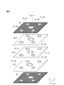
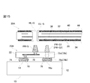
- a printed wiring board (hereinafter simply referred to as “wiring board”) 10 of this embodiment includes an insulating (dielectric) board member 12 having a rectangular main surface.
- the long and short sides of the rectangle forming the main surface of the substrate member 12 extend along the X axis and the Y axis, respectively, and the thickness (height) of the substrate member 12 extends along the Z axis.
- the main surface facing the positive side in the Z-axis direction is referred to as “upper surface” and the main surface facing the negative side in the Z-axis direction is referred to as “lower surface” as necessary.
- a wiring conductor and a ground conductor are embedded in the substrate member 12 (both not shown).
- a single signal terminal 14 electrically connected to the wiring conductor is provided on the upper surface of the substrate member 12, and two ground terminals 16a and 16b electrically connected to the ground conductor are provided.
- Each of the signal terminal 14 and the ground terminals 16a and 16b has a rectangular main surface and is formed in a plate shape.
- the signal terminal 14 and the ground terminals 16a and 16b are arranged in such a manner that the long sides of the rectangles forming the main surfaces are along the X axis and the ground terminals 16a and 16b sandwich the signal terminal 14 in the Y axis direction. It is provided at a predetermined position on the upper surface of the member 12.
- the length of each of the ground terminals 16a and 16b in the X-axis direction exceeds “X1”, and the distance between the ground terminals 16a and 16b in the Y-axis direction corresponds to “Y1”.
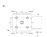
- the connector 20 is provided on the wiring board 10 to fix the flat cable 30 using a flexible insulator (dielectric) 22 formed in a rectangular parallelepiped shape as a base body. It is a fixed part.
- the insulator 22 is manufactured by stacking three insulating sheets SH1 to SH3.
- the upper surface of the insulator 22 is covered with a resist layer 24, and the lower surface of the insulator 22 is covered with a resist layer 26.
- a through hole HL-S reaching the lower surface is formed at the center of the upper surface of the connector 20.
- four through holes HL-G1 to HL-G4 reaching the lower surface are also formed in the vicinity of the four corners of the rectangle forming the upper surface of the connector 20.
- the through hole HL-G1 is formed at the negative corner in the X axis direction and at the positive corner in the Y axis direction
- the through hole HL-G2 is at the positive side in the X axis direction and in the Y axis direction. Is formed at the positive corner.
- the through hole HL-G3 is formed at the negative corner in the X-axis direction and the negative side in the Y-axis direction
- the through-hole HL-G4 is the positive corner in the X-axis direction and the negative corner in the Y-axis direction. Formed.
- the through holes HL-G1 and HL-G2 are arranged along the X axis, and the through holes HL-G3 and HL-G4 are also arranged along the X axis.
- the interval between the through holes HL-G1 and HL-G2 and the interval between the through holes HL-G3 and HL-G4 both correspond to “X1”.
- the through holes HL-G1 and HL-G3 are arranged along the Y axis, and the through holes HL-G2 and HL-G4 are also arranged along the Y axis.
- the interval between the through holes HL-G1 and HL-G3 and the interval between the through holes HL-G2 and HL-G4 both correspond to “Y1”.
- the inner diameters of the through holes HL-G1 to HL-G4 coincide with each other, and the inner diameter of the through hole HL-S is slightly larger than the inner diameter of each of the through holes HL-G1 to HL-
- a conductive film EL-S is formed on the inner peripheral surface of the through hole HL-S.
- a conductive film EL-G1 is formed on the inner peripheral surface of the through hole HL-G1
- a conductive film EL-G2 is formed on the inner peripheral surface of the through hole HL-G2.
- a conductive film EL-G3 is formed on the inner peripheral surface of the through hole HL-G3
- a conductive film EL-G4 is formed on the inner peripheral surface of the through hole HL-G4.
- the inner diameter formed in the resist layers 24 and 26 is slightly larger than the inner diameter formed in the insulator 22.
- a part of the conductive films EL-S, EL-G1 to EL-G4 approaches the upper and lower surfaces of the insulator 22 by the difference in the inner diameter.
- a flat cable (high-frequency transmission line) 30 has a triplate-type stripline structure, and has a flexible thin plate-like insulator (dielectric) 32 as a base.
- the insulator 32 has an arbitrary length along the X axis, and the main surface of the insulator 32 faces the Z axis direction. At the end portion 32t in the X-axis direction, the size of the main surface of the insulator 32 is adjusted to match the size of the main surface of the connector 20.
- the upper surface (main surface facing the positive side in the Z-axis direction) of the insulator 32 is covered with a resist layer 34.
- a signal that protrudes in a solid columnar shape (strictly, a solid truncated cone shape) at a position corresponding to the end 32t on the lower surface of the insulator 32 (main surface facing the negative side in the Z-axis direction).
- Protruding connection conductors for signals (hereinafter referred to as signal columnar conductors) PR-S and protruding connection conductors for ground (hereinafter referred to as ground columnar conductors) PR-G1 to PR-G4 are provided.
- the signal columnar conductor PR-S protrudes from the center of the lower surface of the end portion 32t to the negative side in the Z-axis direction.
- the ground columnar conductors PR-G1 to PR-G4 protrude from the four corners of the lower surface of the end portion 32t to the negative side in the Z-axis direction.
- the outer diameters of the tip portions of the signal columnar conductor PR-S and the ground columnar conductors PR-G1 to PR-G4 are the same as or slightly smaller than the inner diameters of the through holes HL-S and LG-G1 to HL-G4. . Further, the outer diameters of the base portions of the signal columnar conductor PR-S and the ground columnar conductors PR-G1 to PR-G4 are slightly larger than the inner diameters of the through holes HL-S and L-G1 to HL-G4.
- the ground columnar conductor PR-G1 is formed on the negative side in the X-axis direction and on the positive corner in the Y-axis direction, and the ground columnar conductor PR-G2 is on the positive side in the X-axis direction. In addition, it is formed at the positive corner in the Y-axis direction.
- the ground columnar conductor PR-G3 is formed at the negative side corner in the X-axis direction and the negative side in the Y-axis direction, and the ground columnar conductor PR-G4 is formed on the positive side in the X-axis direction and in the Y-axis direction. Formed in the negative corner.
- the ground columnar conductors PR-G1 and PR-G2 are arranged along the X axis, and the ground columnar conductors PR-G3 and PR-G4 are also arranged along the X axis.
- the distance between the ground columnar conductors PR-G1 and PR-G2 and the distance between the ground columnar conductors PR-G3 and PR-G4 correspond to “X1”.
- the ground columnar conductors PR-G1 and PR-G3 are arranged along the Y axis, and the ground columnar conductors PR-G2 and PR-G4 are also arranged along the Y axis.
- the distance between the ground columnar conductors PR-G1 and PR-G3 and the distance between the ground columnar conductors PR-G2 and PR-G4 correspond to “Y1”.
- the dimensions of the ground columnar conductors PR-G1 to PR-G4 coincide with each other.
- the height of the ground columnar conductor PR-S matches the height of each of the ground columnar conductors PR-G1 to PR-G4, but at the same height position, the outer diameter of the ground columnar conductor PR-S is It is slightly larger than the outer diameter of each of the ground columnar conductors PR-G1 to PR-G4.
- the insulator 32 is produced by laminating a resist layer 34 and flexible insulating sheets (dielectric sheets) SH11 to SH13.
- insulating sheets SH11 to SH13 thermoplastic resin sheets such as liquid crystal polymer and polyimide are used. This thermoplastic resin sheet has elasticity and flexibility, and can be integrated by pressure and heat treatment without using an adhesive layer such as an epoxy resin.
- the resist layer 34 and the insulating sheets SH11 to SH13 have the same main surface size, and the vicinity of the end of each main surface is substantially T-shaped when viewed from the Z-axis direction.
- the columnar conductors CD-G11, CD-G21, CD-G31, and CD-G41 are embedded in the insulating sheet SH11, and the ground layer 36 is formed on the lower surface of the insulating sheet SH11.
- the insulating sheet SH12 is embedded with ground columnar conductors CD-G12, CD-G22, CD-G32, CD-G42 and the signal columnar conductor CD-S, and transmits a high-frequency signal to the lower surface of the insulating sheet SH12.
- a plate-shaped transmission conductor 38 is formed.
- the signal columnar conductor PR-S and the ground columnar conductors PR-G1 to PR-G4 are provided on the insulating sheet SH13, and the ground layer 40 and the reinforcing layer 42 are formed on the lower surface of the insulating sheet SH13.
- the ground layer 36, the transmission conductor 38, the ground layer 40, and the reinforcing layer 42 are formed by patterning a metal layer such as a copper foil provided on the main surface of the insulating sheets SH11 to SH13 by etching or the like.
- the ground columnar conductor CD-G11 When the insulating sheet SH11 is viewed from the Z-axis direction, the ground columnar conductor CD-G11 is embedded at a position overlapping the ground columnar conductor PR-G1, and the ground columnar conductor CD-G21 is connected to the ground columnar conductor PR-G2.
- the ground columnar conductor CD-G31 is embedded at a position overlapping the ground columnar conductor PR-G3, and the ground columnar conductor CD-G41 is embedded at a position overlapping the ground columnar conductor PR-G4. .
- the ground layer 36 provided on the lower surface of the insulating sheet SH11 is integrally formed by a plate-like ground conductor 36a that forms a ladder when viewed from the Z-axis direction and a plate-shaped ground conductor 36b that forms a rectangular ring when viewed from the Z-axis direction. Formed.
- the ground conductor 36a extends along the X axis, and the ground conductor 36b is provided at an end portion in the X axis direction.
- the rectangular ring forming the ground conductor 36b overlaps the ground columnar conductors CD-G11, CD-G21, CD-G31, and CD-G41.
- the ground columnar conductor CD-G12 When the insulating sheet SH12 is viewed from the Z-axis direction, the ground columnar conductor CD-G12 is embedded at a position overlapping the ground columnar conductor PR-G1, and the ground columnar conductor CD-G22 is connected to the ground columnar conductor PR-G2. Embedded in the overlapping position, the ground columnar conductor CD-G32 is embedded in a position overlapping with the ground columnar conductor PR-G3, the ground columnar conductor CD-G42 is embedded in a position overlapping with the ground columnar conductor PR-G4, The signal columnar conductor CD-S is embedded at a position overlapping the signal columnar conductor PR-S.
- the transmission conductor 38 provided on the lower surface of the insulating sheet SH12 is integrally formed by a strip-shaped conductor 38a that forms a long band when viewed from the Z-axis direction and a reinforcing conductor 38b that forms a rectangle when viewed from the Z-axis direction.
- the strip-shaped conductor 38a has a width smaller than that of the ground conductor 36a and extends in the X-axis direction, and the reinforcing conductor 38b is provided at an end portion in the X-axis direction.
- the reinforcing conductor 38b is positioned inside the rectangular ring forming the ground conductor 36b and overlaps the signal columnar conductor PR-S.
- the ground layer 40 provided on the lower surface of the insulating sheet SH13 is integrally formed by a ground conductor 40a that forms a long band when viewed from the Z-axis direction and a plate-shaped ground conductor 36b that forms a rectangular ring when viewed from the Z-axis direction. Formed.
- the ground conductor 40a has the same width as the ground conductor 36a and extends in the X-axis direction, and the ground conductor 40b is provided at an end in the X-axis direction. When viewed from the Z-axis direction, the ground conductor 40b overlaps the ground conductor 36b.
- the reinforcing layer 42 is provided inside the rectangular ring forming the ground conductor 40b. When viewed from the Z-axis direction, the reinforcing layer 42 overlaps the signal columnar conductor PR-S.
- the transmission conductor 38 is connected to the signal columnar conductor PR-S via the signal columnar conductor CD-S and the reinforcing layer 42.
- the ground conductor 36 is connected to the ground columnar conductors PR-G1 to PR-G4 via the ground columnar conductors CD-G11 to CD-G41, CD-G12 to CD-G42, and the ground layer 40.
- the ground conductors 40a and 36a are also connected to each other by via-hole conductors (not shown) arranged at equal intervals in the X-axis direction and extending in the Z-axis direction.
- the lower surface side end of through hole HL-S faces signal terminal 14, and the lower surface side ends of through holes HL-G1 and HL-G2 face signal terminal 16a. Then, the lower surface side end portions of the through holes HL-G3 and HL-G4 are placed on the wiring board 10 at positions facing the signal terminals 16b. The through holes and terminals facing each other are coupled and electrically connected by a conductive bonding material 50 such as solder paste. The connector 20 is thus fixed to the wiring board 10.
- the signal columnar conductor PR-S When the flat cable 30 is connected to the connector 20, the signal columnar conductor PR-S is inserted into the through hole HL-S, and the ground columnar conductors PR-G1 to PR-G4 are inserted into the through holes HL-G1 to HL-G4. Each inserted.
- a conductive bonding material 52 is printed on the tip of each of the signal columnar conductor PR-S and the ground columnar conductors PR-G1 to PR-G4, and is melted by heat treatment after insertion. The mutually opposing conductor and through-hole are electrically connected via a molten conductive bonding material 52.
- the signal columnar conductor PR-S and the ground columnar conductors PR-G1 to PR-G4 are harder than the insulator 22 forming the connector 20, and the signal columnar conductor PR-S and the ground columnar conductors PR-G1 to PR-G4.
- the through holes HL-S, HL-G1 to HL-G4 are used as the signal columnar conductor PR-S and the ground columnar conductor PR-G1 to PR.
- -Deform according to the shape of G4.
- the signal columnar conductor PR-S, the ground columnar conductors PR-G1 to PR-G4 and the through holes HL-S and HL-G1 to HL-G4 are maintained in a strong and good electrical contact state. Connected.
- the signal columnar conductor PR-S and the ground columnar conductors PR-G1 to PR-G4 are formed in a truncated cone shape, the signal columnar conductor PR-S and the ground columnar conductors PR-G1 to PR-G4 are formed. Are easily pierced into the through holes HL-S and HL-G1 to HL-G4. Instead of the signal columnar conductor PR-S and the ground columnar conductors PR-G1 to PR-G4, the inner peripheral surfaces of the through holes HL-S and L-G1 to HL-G4 may be tapered. Good.
- the conductive bonding material 52 is not always necessary.
- the flat cable 30 and the connector 20 may be fixed with a non-conductive adhesive or a pin.
- the wiring board 10 on which the connector 20 is mounted is housed in, for example, the housing CB1 of the mobile communication terminal 60.
- the flat cable 30 is mounted on the wiring board 10 as described above.
- the circuits or elements mounted on the wiring board 10 are connected to each other via the flat cable 30. Since the flat cable 30 is thin and flexible, it is particularly useful when only a thin gap can be secured in the housing CB1.
- the connector 20 is manufactured in the manner shown in FIGS. 10 (A) to 10 (E).
- three insulating sheets SH1 to SH3 having a common size are stacked (see FIG. 10A).
- thermoplastic resin sheets such as liquid crystal polymer and polyimide are used. Since the thermoplastic resin sheet has elasticity and flexibility, the insulating sheets SH1 to SH3 can be fused and integrated by applying pressure and heat treatment without using an adhesive layer such as an epoxy resin. .
- Resist layers 24 and 26 are formed on the upper and lower surfaces of the insulator 22 thus fabricated (see FIG. 10B).
- the resist layers 24 and 26 are etched at the positions where the through holes HL-S and HL-G1 to HL-G4 are to be formed, and a part of the insulator 22 is exposed on the upper surface and the lower surface (FIG. 10C )reference).
- through holes HL-S, HL-G1 to HL-G4 are formed by laser irradiation or the like (see FIG. 10D), and thereafter conductive films EL-S, EL-G1 to EL-G4 are formed by plating.
- conductive films EL-S, EL-G1 to EL-G4 are formed by plating.
- the flat cable 30 is manufactured as shown in FIGS. 11 (A) to 11 (C).
- the copper foil formed on the insulating sheet SH11 is patterned by etching or the like to form the ground layer 36, and four holes are formed in the insulating sheet SH11 corresponding to the positions of the ground columnar conductors CD-G11 to CD-G41.
- the four holes are filled with a conductive paste (not shown) in which copper powder is dispersed (see FIG. 11A).
- the copper foil formed on the insulating sheet SH12 is patterned by etching or the like to form the transmission conductor 38, corresponding to the positions of the signal columnar conductor CD-S and the ground columnar conductors CD-G12 to CD-G42. Then, five holes are formed in the insulating sheet SH12, and the five holes are filled with a conductive paste PS1 obtained by dispersing copper powder (see FIG. 11A).
- the copper foil formed on the insulating sheet SH13 is patterned by etching or the like to form the ground layer 40 and the reinforcing layer 42.
- the signal columnar conductor PR-S and the ground columnar conductors PR-G1 to PR-G4 are formed.
- five holes are formed in the insulating sheet SH13, and the five holes are filled with the conductive paste PS2 formed by dispersing copper powder (see FIG. 11A).
- a conductive paste PS3 is formed by forming five holes in the auxiliary sheet SH14 corresponding to the positions of the signal columnar conductor PR-S and the ground columnar conductors PR-G1 to PR-G4 and dispersing copper powder. The five holes are filled (see FIG. 11A). The five holes are penetrated from the lower surface to the upper surface, and the conductive paste PS3 is filled from the lower surface. This operation is performed with the lower surface of the auxiliary sheet SH14 facing upward.
- the metal powders contained in the conductive pastes PS1 to PS3 and the conductive paste have the same composition, and copper powder and silver powder are used.
- the insulating sheets SH11 to SH13 and the auxiliary sheet SH14 are laminated in this order, and the resulting laminated body is pressurized and heated (see FIG. 11B).
- the insulating sheets SH11 to SH13 are fused and integrated to produce the insulator 22.
- the metal powder contained in the conductive paste filled in the other holes as described above and the metal powder contained in the conductive pastes PS1 to PS3 are metallized by sintering, so that the signal columnar conductors PR-S, CD-S, ground columnar conductors PR-G1 to PR-G4, CD-G11 to CD-G41, and CD-G12 to CD-G42 are produced.
- the auxiliary sheet SH14 is not integrated with the insulating sheet SH13.
- a thermoplastic resin sheet integrated at about 300 ° C. such as a liquid crystal polymer or polyimide
- a fluorine resin sheet can be used as the auxiliary sheet SH14.
- the material of the fluororesin sheet include polytetrafluoroethylene (PTFE), PTFE-perfluoroalkyl vinyl ether copolymer, PTFE-hexafluoropropylene copolymer, PTFE-ethylene copolymer, and the like. it can.
- other materials may be used for the auxiliary sheet SH14 as long as they are not joined and integrated with the insulating sheets SH11 to SH13 during the pressurizing / heating treatment.
- the auxiliary sheet SH14 is peeled off, and a resist layer 34 is formed on the lower surface of the insulator 32 (see FIG. 11C).
- the signal columnar conductor PR-S and the ground columnar conductors PR-G1 to G4 appear on the upper surface of the insulator 32 by peeling off the auxiliary sheet SH14.
- processing such as plating is performed in this state.
- plating films are formed on the surfaces of the signal columnar conductor PR-S and the ground columnar conductors PR-G1 to G4, the surfaces thereof become smooth and the strength of the protruding conductor itself is improved.
- the signal columnar conductor PR-S and the ground columnar conductors PR-G1 to PR-G4 are formed in a truncated cone shape.
- the side surface of the hole can be tapered by adjusting the intensity of the laser, and this is used to form a truncated cone.
- the diameter on the bottom surface side of each conductor is adjusted to 200 to 500 ⁇ m
- the diameter on the top surface side of each conductor is adjusted to about 100 to 300 ⁇ m
- the height of each conductor is adjusted to about 25 ⁇ m to 1 mm.
- the height of each conductor depends on the thickness of the auxiliary sheet SH14.
- the signal columnar conductor PR-S protruding from the insulator 32 is integrated with the signal columnar conductor CD-S embedded in the insulator 32, and the ground columnar conductor PR-G1 protruding from the insulator 32 is used.
- PR-G4 are also integrated with signal columnar conductors CD-G11 to CD-G41, CD-G12 to CD-G42 embedded in the insulator 32. Therefore, the signal columnar conductor PR-S and the ground columnar conductors PR-G1 to PR-G4 are not easily dropped from the insulator 32, and the strength is improved.
- the strength of the end portion 32t can be increased while maintaining the flexibility of the line portion.
- the conductor density at the end portion 32t may be increased.
- the signal columnar conductor PR-S and the ground columnar conductors PR-G1 to PR-G4 are obtained by metallizing the conductive pastes PS2 and PS3. It is formed.
- the reinforcing layer 80 is sandwiched between the conductive pastes PS2 and PS3 as shown in FIG.
- the conductive pastes PS2 and PS3 may be metallized.
- the flat cable 30 has the insulator 32 as a base material and has a long transmission conductor 38 and ground layers 36 and 40.
- the connector 20 is provided on the wiring board 10 to fix the flat cable 30.
- the flat cable 30 has signal columnar conductors PR-S and CD-S formed integrally with the transmission conductor 38 and in the form of a solid column, and is also integral with the ground layers 36 and 40 and the medium.
- the connector 20 includes a through hole HL-S having a shape corresponding to the shape of the signal columnar conductor PR-S, and a through hole HL-G1 having a shape corresponding to the shapes of the ground columnar conductors PR-G1 to PR-G4.
- HL-G4 A conductive film EL-S is formed on the inner peripheral surface of the through hole HL-S, and conductive films EL-G1 to EL-G4 are formed on the inner peripheral surface of the through holes HL-G1 to HL-G4.
- the signal columnar conductor PR-S is inserted into the through hole HL-S, and the ground columnar conductors PR-G1 to PR-G4 are inserted into the through holes HL-G1 to HL-G4.
- the flat cable 30 may be manufactured in the manner shown in FIGS. 13 (A) to 13 (D).
- a conductive material (not shown) is filled in four holes formed in the insulating sheet SH11 corresponding to the positions of the ground columnar conductors CD-G11 to CD-G41, and a ground layer is formed on the lower surface of the insulating sheet SH11. 36 is formed (see FIG. 13A).
- the conductive material PS1 is filled in the five holes formed in the insulating sheet SH12 corresponding to the positions of the signal columnar conductor CD-S and the ground columnar conductors CD-G12 to CD-G42, and the insulating sheet SH12 A transmission conductor 38 is formed on the lower surface (see FIG. 13A).
- the conductive material PS2 is filled in the five holes formed in the insulating sheet SH13 corresponding to the positions of the signal columnar conductor PR-S and the ground columnar conductors PR-G1 to PR-G4.
- a ground layer 40 and a reinforcing layer 42 are formed on the lower surface (see FIG. 13A).
- the insulating sheets SH11 to SH13 are stacked in this order and thermocompression bonded, and resist layers RL1 and 34 are formed on the upper surface and the lower surface of the insulator 32 thus manufactured (see FIG. 13B).
- the conductive material (not shown) filled in the above-described manner and the conductive materials PS1 to PS2 are metallized, and part of the signal columnar conductor PR-S and ground columnar conductors PR-G1 to PR-G4
- the signal columnar conductor CD-S, the ground columnar conductors CD-G11 to CD-G41, and CD-G12 to CD-G42 are formed.
- the resist layer RL1 is etched corresponding to the positions of the signal columnar conductor PR-S and the ground columnar conductors PR-G1 to PR-G4.
- plating is performed at the etched position to form other portions of the signal columnar conductor PR-S and the ground columnar conductors PR-G1 to PR-G4 (see FIG. 13C).
- the resist layer RL1 is removed (see FIG. 13D), whereby the flat cable 30 is completed.
- the through holes HL-S, HL-G1 to HL-G4 are formed in the connector 20, and the solid columnar columnar conductors PR-S, PR-G1 to PR-G4 are formed in the flat cable 30.
- the solid columnar columnar conductors PR-S, PR-G1 to PR-G4 are formed in the flat cable 30.
- through holes HL-S, HL-G1 to HL-G2 are formed in the flat cable 30A, and the solid columnar columnar conductors PR-S and PR-G1 are formed in the connector 20A.
- ⁇ PR-G2 may be formed.
- the flat cable 30A and the connector 20A according to the present embodiment will be described with reference to FIGS. The same components as those of the flat cable 30 and the connector 20 are given the same reference numerals, and detailed description thereof is omitted.
- the signal columnar conductor PR-S is formed so as to protrude upward from a position on the negative side in the X-axis direction from the center of the upper surface of the connector 20A.
- the ground columnar conductor PR-G1 is formed so as to protrude from the positive side corner in the X-axis direction and the positive side in the Y-axis direction of the upper surface of the connector 20A, and the ground columnar conductor PR-G2 is a connector.
- the upper surface of 20A is formed so as to protrude upward from a corner on the positive side in the X-axis direction and on the negative side in the Y-axis direction.
- the through hole HL-S is formed at a position on the negative side in the X-axis direction from the center of the main surface of the end portion 32t.
- the through hole HL-G1 is formed at the corner on the positive side in the X-axis direction and the positive side in the Y-axis direction of the main surface of the end portion 32t, and the through-hole HL-G2 is formed on the main surface of the end portion 32t in the X-axis direction. It is formed at the corner on the positive side in the direction and on the negative side in the Y-axis direction.
- the conductive film EL-S is formed on the inner peripheral surface of the through hole HL-S, and the conductive films EL-G1 to EL-G2 are formed on the inner peripheral surface of the through holes HL-G1 to HL-G2. .
- the through-hole in which the conductive film is formed on the inner peripheral surface functions as a hole-shaped connection conductor into which the protruding connection conductor is inserted.
- the signal columnar conductor PR-S is integrated with the connection conductor 70
- the ground columnar conductor PR-G1 is integrated with the connection conductor 72a
- the ground columnar conductor PR-G2 is integrated with the connection conductor. 72b.
- a signal terminal 74 and ground terminals 76 a and 76 b are provided on the lower surface of the insulator 22.
- the signal terminal 74 is electrically connected to the connection conductor 70
- the ground terminals 76a and 76b are electrically connected to the connection conductors 72a and 72b, respectively.
- the signal terminal 74 is electrically connected to the signal terminal 14 of the wiring board 10 by the conductive bonding material 78, and the connection conductors 76 a and 76 b are electrically connected to the ground terminals 16 a and 16 b of the wiring board 10 by the conductive bonding material 78. Connected to.
- the through hole HL-S further penetrates the transmission conductor 38, and each of the through holes HL-G1 and HL-G2 further penetrates the ground layers 36 and 40. Therefore, the transmission conductor 38 is electrically connected to the conductive film EL-S, and the ground layers 36 and 40 are electrically connected to each of the conductive films EL-G1 and EL-G2.
- a single signal columnar conductor PR-S is formed on the lower surface of the insulating sheet SH13 (the main surface facing the negative side in the Z-axis direction), and the signal columnar conductor PR-S and A single signal columnar conductor CD-S electrically connected is embedded in the insulating sheet SH12, and a single transmission conductor 38 electrically connected to the signal columnar conductor CD-S is formed on the insulating sheet SH12. It is formed on the upper surface (the main surface facing the positive side in the Z-axis direction) (see FIG. 6).
- a plurality of signal columnar conductors PR-S1 to PR-S3 are formed on the lower surface of the insulating sheet SH13 in place of the signal columnar conductor PR-S of the flat cable 30 as in the flat cable 30B shown in FIG.
- a plurality of signal columnar conductors CD-S1 to CD-S3 respectively connected to the plurality of signal columnar conductors PR-S1 to PR-S3 are embedded in the insulating sheet SH12 in place of the signal columnar conductor CD-S, and the signal A plurality of transmission conductors 38a to 38c respectively connected to the columnar conductors CD-S1 to CD-S3 may be formed on the upper surface of the insulating sheet SH12 instead of the transmission conductor 38.
- the flat cable 30B and the connector 20B of the present embodiment will be described with reference to FIGS. The same components as those of the flat cable 30 and the connector 20 are given the same reference numerals, and detailed description thereof is omitted.
- the signal columnar conductor PR-S2 protrudes from the center of the lower surface of the end portion of the flat cable 30B to the negative side in the Z-axis direction. Further, the signal columnar conductor PR-S1 protrudes from the position on the positive side in the Y-axis direction to the negative side in the Z-axis direction from the signal columnar conductor PR-S2, and the signal columnar conductor PR-S3 is projected on the signal columnar conductor PR. Projects to the negative side in the Z-axis direction from the negative side position in the Y-axis direction from -S2.
- the signal columnar conductor CD-S1 is embedded at a position overlapping the signal columnar conductor PR-S1 when viewed from the Z-axis direction, and the signal columnar conductor CD-S2 is viewed from the Z-axis direction.
- the signal columnar conductor CD-S3 is embedded at a position overlapping with the signal columnar conductor PR-S3 when viewed from the Z-axis direction.
- each of the transmission conductors 38a to 38c is arranged in the positive direction of the Y axis in the order of 38c ⁇ 38b ⁇ 38a.
- the end of the transmission conductor 38a overlaps with the signal columnar conductor CD-S1 when viewed from the Z-axis direction
- the end of the transmission conductor 38b overlaps with the signal columnar conductor CD-S2 when viewed from the Z-axis direction.
- the end portion overlaps with the signal columnar conductor CD-S3 when viewed from the Z-axis direction.
- the reinforcing layer 42 is omitted.
- the connector 20B to which such a flat cable 30B is attached is configured as shown in FIG. According to FIG. 17, through holes HL-S 1 to HL-S 3 are formed instead of the through holes HL-S of the connector 20.
- the through hole HL-S2 extends from the center position of the upper surface of the connector 20B in the Z-axis direction and reaches the lower surface of the connector 20B.
- the through hole HL-S1 extends in the Z axis direction from a position on the positive side in the Y axis direction than the through hole HL-S2 and reaches the lower surface of the connector 20B.
- the through hole HL-S3 extends in the Z-axis direction from the position on the negative side in the Y-axis direction than the through-hole HL-S2, and reaches the lower surface of the connector 20B.
- a conductive film EL-S1 is formed on the inner peripheral surface of the through hole HL-S1
- a conductive film EL-S2 is formed on the inner peripheral surface of the through hole HL-S2
- the inner surface of the through hole HL-S3 is formed.
- a conductive film EL-S3 is formed on the peripheral surface.
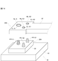
- the camera module 90 includes a thermoplastic module substrate 92 that is formed by layers larger than the number of layers of the flat cable 30B and is slightly harder than the flat cable 30B.
- the connector 20B is mounted on such a module substrate 92.
- the module substrate 92 is also mounted with an image sensor IC 94 and a lens unit 96 having a lens 98.
- the module substrate 92 further incorporates passive elements such as the inductor elements 100 and 102.
- columnar conductors PR-S1 to PR-S3, PR-G1 to PR-G4 are formed in the flat cable 30B, and the through holes HL-S1 to HL-S3 and HL-G1 to HL are formed in the connector 20B. -G4 is formed.
- the columnar conductors PR-S1 to PR-S3, PR-G1 to PR-G2 are formed in the connector 20B, and the through holes HL-S1 to HL-S3 and HL-G1 to HL-G2 are formed in the flat cable 30B. You may do it.
- the single signal columnar conductor PR-S is formed so as to protrude upward from the position on the negative side in the X-axis direction from the center of the upper surface of the connector 20A, and the conductive film EL- A single through hole HL-S having an inner peripheral surface on which S is formed is formed at a position on the negative side in the X-axis direction from the center of the main surface of the end portion 32t of the cable 30A.
- a plurality of signal columnar conductors are formed in the connector 20A instead of the signal columnar conductors PR_S, and a plurality of through holes are formed in the cable 30A instead of the through holes HL_S.
- These transmission conductors may be formed on the cable 30 ⁇ / b> A instead of the transmission conductor 38.
- a plurality of connection conductors respectively integrated with a plurality of signal columnar conductors are provided in the connector 20A instead of the connection conductor 70, and a plurality of signal terminals respectively connected to the plurality of connection conductors are the signal terminals 74. Instead, it is provided in the connector 20A. Further, the plurality of signal terminals provided on the connector 20A are respectively connected to the plurality of signal terminals provided on the wiring board 10 for signal transmission. In the flat cable 30A, the plurality of through holes respectively penetrate the plurality of transmission conductors.
- the element body of the flat cable and the element body of the connector substrate may be laminated and integrated with a plurality of insulating sheets without using an adhesive layer as described above. It may be laminated and integrated using an adhesive layer.
- a laminated flat cable for example, a single-layer flat cable (microstrip line type) having a signal line conductor on the front surface and a ground conductor on the back surface may be used.
- a normal stripline structure in which the ground layers are arranged symmetrically around the signal line conductor may be used.
- This cable is widely used mainly as a signal line for transmitting a high-frequency signal, and is not limited to a cable for connecting a power feeding circuit (RFIC) and an antenna element.
- RFIC power feeding circuit
- the ground layer and the signal line conductor may be formed by patterning a metal thin film of a single-sided metal-clad sheet or a double-sided metal-clad sheet by etching or the like, and a conductive paste is pattern-printed using a screen plate or the like. It may be a thing.
- interlayer connection conductor for connecting the two ground layers is not limited to the via hole conductor as described above, and may be a through hole conductor.
- the through-hole conductor is a through-type interlayer connection conductor in which conductivity is imparted to a through-hole penetrating the element body by plating or the like.
- the connector with the hole connection conductor is provided separately from the wiring board which is the mother board.
- the hole connection conductor is provided on the wiring board itself, and the flat conductor protruding conductor is connected to the wiring board without using the connector. You may comprise so that a hole-shaped connection conductor may pierce directly. That is, the connector may be the wiring board itself. In this case, the hole-shaped connecting conductor of the wiring board serves as a fixing portion for fixing the cable.
Abstract
Priority Applications (4)
| Application Number | Priority Date | Filing Date | Title |
|---|---|---|---|
| CN201390000587.5U CN204597019U (zh) | 2012-06-29 | 2013-04-23 | 将电缆固定于布线基板的固定结构、以及电缆 |
| JP2014522465A JP5900766B2 (ja) | 2012-06-29 | 2013-04-23 | ケーブルの配線基板への固定構造または固定方法 |
| US14/564,143 US9647312B2 (en) | 2012-06-29 | 2014-12-09 | Fixing structure of cable to wiring substrate, and cable, and manufacturing method of cable |
| US15/456,698 US10855010B2 (en) | 2012-06-29 | 2017-03-13 | Fixing structure of cable to wiring substrate, and cable, and manufacturing method of cable |
Applications Claiming Priority (2)
| Application Number | Priority Date | Filing Date | Title |
|---|---|---|---|
| JP2012-147022 | 2012-06-29 | ||
| JP2012147022 | 2012-06-29 |
Related Child Applications (1)
| Application Number | Title | Priority Date | Filing Date |
|---|---|---|---|
| US14/564,143 Continuation US9647312B2 (en) | 2012-06-29 | 2014-12-09 | Fixing structure of cable to wiring substrate, and cable, and manufacturing method of cable |
Publications (1)
| Publication Number | Publication Date |
|---|---|
| WO2014002592A1 true WO2014002592A1 (fr) | 2014-01-03 |
Family
ID=49782768
Family Applications (1)
| Application Number | Title | Priority Date | Filing Date |
|---|---|---|---|
| PCT/JP2013/061839 WO2014002592A1 (fr) | 2012-06-29 | 2013-04-23 | Structure pour apposer un câble sur un panneau de câblage, câble, et procédé de fabrication de câble |
Country Status (4)
| Country | Link |
|---|---|
| US (2) | US9647312B2 (fr) |
| JP (1) | JP5900766B2 (fr) |
| CN (1) | CN204597019U (fr) |
| WO (1) | WO2014002592A1 (fr) |
Cited By (4)
| Publication number | Priority date | Publication date | Assignee | Title |
|---|---|---|---|---|
| WO2018180413A1 (fr) * | 2017-03-31 | 2018-10-04 | 株式会社村田製作所 | Dispositif électronique |
| US10701805B2 (en) | 2016-02-24 | 2020-06-30 | Murata Manufacturing Co., Ltd. | Composite substrate, method of manufacturing composite substrate, and method of manufacturing flexible board |
| US11145586B2 (en) | 2017-11-01 | 2021-10-12 | Murata Manufacturing Co., Ltd. | Interposer and electronic device |
| US11166372B2 (en) | 2017-05-16 | 2021-11-02 | Murata Manufacturing Co., Ltd. | Electronic device |
Families Citing this family (6)
| Publication number | Priority date | Publication date | Assignee | Title |
|---|---|---|---|---|
| CN210130017U (zh) * | 2016-01-20 | 2020-03-06 | 株式会社村田制作所 | 树脂多层基板与电路基板的接合构造 |
| JP6849670B2 (ja) * | 2016-04-26 | 2021-03-24 | 京セラ株式会社 | 半導体パッケージおよびそれを用いた半導体装置 |
| US10788515B2 (en) | 2016-12-21 | 2020-09-29 | Itron, Inc. | Multi-piece current shunt with conductive channel for uniform current flow |
| WO2018213494A1 (fr) * | 2017-05-16 | 2018-11-22 | Rigetti & Co, Inc. | Connexion de circuits électriques dans un système informatique quantique |
| KR101938104B1 (ko) * | 2018-01-25 | 2019-01-14 | 주식회사 기가레인 | 접합 평탄도가 개선된 연성회로기판 |
| EP3755126A4 (fr) * | 2018-03-15 | 2021-03-03 | Huawei Technologies Co., Ltd. | Plaque de connexion, ensemble carte de circuit imprimé et dispositif électronique |
Citations (5)
| Publication number | Priority date | Publication date | Assignee | Title |
|---|---|---|---|---|
| JPH03101015U (fr) * | 1990-01-31 | 1991-10-22 | ||
| JPH06326209A (ja) * | 1993-05-14 | 1994-11-25 | Matsushita Electric Ind Co Ltd | 半導体実装用セラミック基板の製造方法 |
| JPH11149952A (ja) * | 1997-11-17 | 1999-06-02 | Japan Aviation Electron Ind Ltd | スルーホールタイプfpc接続用コネクタ |
| JP4059522B1 (ja) * | 2006-10-27 | 2008-03-12 | 株式会社旭電化研究所 | 電気接続構造、それに用いる第1の接続部材 |
| WO2010047141A1 (fr) * | 2008-10-21 | 2010-04-29 | 株式会社旭電化研究所 | Connecteur femelle, connecteur mâle assemblé sur celui-ci et appareil électrique/électronique utilisant les connecteurs |
Family Cites Families (11)
| Publication number | Priority date | Publication date | Assignee | Title |
|---|---|---|---|---|
| JPS59121868U (ja) * | 1983-02-02 | 1984-08-16 | 株式会社山武 | 電極パタ−ンの連結構造 |
| JPH028860U (fr) | 1988-06-30 | 1990-01-19 | ||
| US5631446A (en) * | 1995-06-07 | 1997-05-20 | Hughes Electronics | Microstrip flexible printed wiring board interconnect line |
| US5689216A (en) * | 1996-04-01 | 1997-11-18 | Hughes Electronics | Direct three-wire to stripline connection |
| JPH10335811A (ja) * | 1997-05-29 | 1998-12-18 | Nec Home Electron Ltd | 基板接続方法 |
| US6933450B2 (en) * | 2002-06-27 | 2005-08-23 | Kyocera Corporation | High-frequency signal transmitting device |
| US6930240B1 (en) * | 2004-03-18 | 2005-08-16 | Agilent Technologies, Inc. | Flex-circuit shielded connection |
| CN101238244B (zh) * | 2005-01-24 | 2011-03-30 | 株式会社昭和 | 采用阳极电解氧化处理的结晶性氧化钛被膜的制造方法 |
| JP5024449B2 (ja) | 2008-04-23 | 2012-09-12 | 株式会社村田製作所 | 同軸コネクタ用レセプタクル |
| WO2010086956A1 (fr) * | 2009-01-27 | 2010-08-05 | エヌワイ工業株式会社 | Structure de connexion de substrat flexible et d'élément opposé |
| JP5310239B2 (ja) * | 2009-05-09 | 2013-10-09 | 富士通株式会社 | 接続端子および伝送線路 |
-
2013
- 2013-04-23 WO PCT/JP2013/061839 patent/WO2014002592A1/fr active Application Filing
- 2013-04-23 JP JP2014522465A patent/JP5900766B2/ja not_active Expired - Fee Related
- 2013-04-23 CN CN201390000587.5U patent/CN204597019U/zh not_active Expired - Lifetime
-
2014
- 2014-12-09 US US14/564,143 patent/US9647312B2/en active Active
-
2017
- 2017-03-13 US US15/456,698 patent/US10855010B2/en active Active
Patent Citations (5)
| Publication number | Priority date | Publication date | Assignee | Title |
|---|---|---|---|---|
| JPH03101015U (fr) * | 1990-01-31 | 1991-10-22 | ||
| JPH06326209A (ja) * | 1993-05-14 | 1994-11-25 | Matsushita Electric Ind Co Ltd | 半導体実装用セラミック基板の製造方法 |
| JPH11149952A (ja) * | 1997-11-17 | 1999-06-02 | Japan Aviation Electron Ind Ltd | スルーホールタイプfpc接続用コネクタ |
| JP4059522B1 (ja) * | 2006-10-27 | 2008-03-12 | 株式会社旭電化研究所 | 電気接続構造、それに用いる第1の接続部材 |
| WO2010047141A1 (fr) * | 2008-10-21 | 2010-04-29 | 株式会社旭電化研究所 | Connecteur femelle, connecteur mâle assemblé sur celui-ci et appareil électrique/électronique utilisant les connecteurs |
Cited By (6)
| Publication number | Priority date | Publication date | Assignee | Title |
|---|---|---|---|---|
| US10701805B2 (en) | 2016-02-24 | 2020-06-30 | Murata Manufacturing Co., Ltd. | Composite substrate, method of manufacturing composite substrate, and method of manufacturing flexible board |
| WO2018180413A1 (fr) * | 2017-03-31 | 2018-10-04 | 株式会社村田製作所 | Dispositif électronique |
| JPWO2018180413A1 (ja) * | 2017-03-31 | 2019-11-07 | 株式会社村田製作所 | 電子機器 |
| US11178765B2 (en) | 2017-03-31 | 2021-11-16 | Murata Manufacturing Co., Ltd. | Electronic device |
| US11166372B2 (en) | 2017-05-16 | 2021-11-02 | Murata Manufacturing Co., Ltd. | Electronic device |
| US11145586B2 (en) | 2017-11-01 | 2021-10-12 | Murata Manufacturing Co., Ltd. | Interposer and electronic device |
Also Published As
| Publication number | Publication date |
|---|---|
| US9647312B2 (en) | 2017-05-09 |
| JP5900766B2 (ja) | 2016-04-06 |
| JPWO2014002592A1 (ja) | 2016-05-30 |
| US20150091676A1 (en) | 2015-04-02 |
| US10855010B2 (en) | 2020-12-01 |
| CN204597019U (zh) | 2015-08-26 |
| US20170187132A1 (en) | 2017-06-29 |
Similar Documents
| Publication | Publication Date | Title |
|---|---|---|
| JP5900766B2 (ja) | ケーブルの配線基板への固定構造または固定方法 | |
| US9673501B2 (en) | Laminated flat cable and method for producing same | |
| JP5794445B2 (ja) | 高周波伝送線路の接続・固定方法 | |
| JPWO2014125988A1 (ja) | 高周波信号伝送線路、電子機器及び高周波信号伝送線路の製造方法 | |
| JP2008085310A (ja) | 多層プリント配線基板 | |
| CN107516764B (zh) | 天线结构及其制作方法 | |
| GB2516568A (en) | High frequency signal transmission line and electronic apparatus | |
| WO2014199886A1 (fr) | Appareil de communication et dispositif électronique | |
| US9401533B2 (en) | Flat cable | |
| CN102316681A (zh) | 电路板及其制作方法 | |
| US20230291086A1 (en) | Transmission line and electronic device | |
| KR20190099728A (ko) | 인쇄회로기판 | |
| JP2007335675A (ja) | 電源装置および電源装置の製造方法 | |
| JPWO2018131383A1 (ja) | アンテナモジュール | |
| JP2011151103A (ja) | 電子部品相互の接続構造及び接続方法 | |
| JP2019021863A (ja) | 多層基板 | |
| JP2015185550A (ja) | 多層高周波基板、アンテナ装置 | |
| JPH11176253A (ja) | フラット型ケーブル | |
| US11145586B2 (en) | Interposer and electronic device | |
| US10772204B2 (en) | Electronic device | |
| JP2013085006A (ja) | 回路基板 | |
| JP2014157857A (ja) | 部品内蔵樹脂多層基板およびその製造方法 | |
| KR20090056173A (ko) | 양면 인쇄회로기판 및 그의 제조 방법 | |
| JP2006179833A (ja) | 配線基板およびその製造方法 | |
| WO2022123996A1 (fr) | Substrat multicouche souple et son procédé de fabrication |
Legal Events
| Date | Code | Title | Description |
|---|---|---|---|
| WWE | Wipo information: entry into national phase |
Ref document number: 201390000587.5 Country of ref document: CN |
|
| 121 | Ep: the epo has been informed by wipo that ep was designated in this application |
Ref document number: 13810863 Country of ref document: EP Kind code of ref document: A1 |
|
| ENP | Entry into the national phase |
Ref document number: 2014522465 Country of ref document: JP Kind code of ref document: A |
|
| NENP | Non-entry into the national phase |
Ref country code: DE |
|
| 122 | Ep: pct application non-entry in european phase |
Ref document number: 13810863 Country of ref document: EP Kind code of ref document: A1 |