WO2013176252A1 - 巻芯及びロール - Google Patents
巻芯及びロール Download PDFInfo
- Publication number
- WO2013176252A1 WO2013176252A1 PCT/JP2013/064476 JP2013064476W WO2013176252A1 WO 2013176252 A1 WO2013176252 A1 WO 2013176252A1 JP 2013064476 W JP2013064476 W JP 2013064476W WO 2013176252 A1 WO2013176252 A1 WO 2013176252A1
- Authority
- WO
- WIPO (PCT)
- Prior art keywords
- adhesive layer
- adhesive
- core
- tape
- layer
- Prior art date
- Legal status (The legal status is an assumption and is not a legal conclusion. Google has not performed a legal analysis and makes no representation as to the accuracy of the status listed.)
- Ceased
Links
Images


Classifications
-
- C—CHEMISTRY; METALLURGY
- C09—DYES; PAINTS; POLISHES; NATURAL RESINS; ADHESIVES; COMPOSITIONS NOT OTHERWISE PROVIDED FOR; APPLICATIONS OF MATERIALS NOT OTHERWISE PROVIDED FOR
- C09J—ADHESIVES; NON-MECHANICAL ASPECTS OF ADHESIVE PROCESSES IN GENERAL; ADHESIVE PROCESSES NOT PROVIDED FOR ELSEWHERE; USE OF MATERIALS AS ADHESIVES
- C09J7/00—Adhesives in the form of films or foils
- C09J7/20—Adhesives in the form of films or foils characterised by their carriers
-
- B—PERFORMING OPERATIONS; TRANSPORTING
- B65—CONVEYING; PACKING; STORING; HANDLING THIN OR FILAMENTARY MATERIAL
- B65H—HANDLING THIN OR FILAMENTARY MATERIAL, e.g. SHEETS, WEBS, CABLES
- B65H75/00—Storing webs, tapes, or filamentary material, e.g. on reels
- B65H75/02—Cores, formers, supports, or holders for coiled, wound, or folded material, e.g. reels, spindles, bobbins, cop tubes, cans, mandrels or chucks
- B65H75/04—Kinds or types
- B65H75/08—Kinds or types of circular or polygonal cross-section
- B65H75/10—Kinds or types of circular or polygonal cross-section without flanges, e.g. cop tubes
-
- C—CHEMISTRY; METALLURGY
- C09—DYES; PAINTS; POLISHES; NATURAL RESINS; ADHESIVES; COMPOSITIONS NOT OTHERWISE PROVIDED FOR; APPLICATIONS OF MATERIALS NOT OTHERWISE PROVIDED FOR
- C09J—ADHESIVES; NON-MECHANICAL ASPECTS OF ADHESIVE PROCESSES IN GENERAL; ADHESIVE PROCESSES NOT PROVIDED FOR ELSEWHERE; USE OF MATERIALS AS ADHESIVES
- C09J2203/00—Applications of adhesives in processes or use of adhesives in the form of films or foils
- C09J2203/326—Applications of adhesives in processes or use of adhesives in the form of films or foils for bonding electronic components such as wafers, chips or semiconductors
Definitions
- the present invention relates to a winding core around which an adhesive tape is wound and a roll around which the adhesive tape is wound.
- the semiconductor device is manufactured by dicing a wafer into chips and bonding the chips to a substrate or the like.
- a die bonding film for bonding the diced chips Is used.
- the dicing die bonding integrated tape described in Patent Document 1 has a die bonding film laminated on a release film and a dicing tape laminated on the die bonding film.
- the dicing tape is formed larger than the die bonding film so as to cover the die bonding film.
- Such a dicing die bonding integrated tape is stored and transported as a roll wound around a cylindrical core.
- the dicing die bonding integrated tape as described above has a step at the boundary between the part where the die bonding film and the dicing tape are laminated on the release film and the part where only the dicing tape is laminated on the release film. Occurs. Moreover, a level
- a dicing / die bonding integrated tape in which a die bonding film and a dicing tape are integrated into one film is also being researched and developed. However, even with such a dicing and die bonding integrated tape, a step is generated, and the same problem as described above occurs.
- an object of the present invention is to provide a winding core and a roll that can suppress the generation of transfer marks and can prevent winding deviation of an adhesive tape.
- a winding core according to the present invention is a cylindrical winding core that winds an adhesive tape having an adhesive layer formed on a long base film along the longitudinal direction of the base film into a plurality of layers.
- the outer diameter of the adhesive is between the inner tape portion and the outer tape portion of the adhesive tape adjacent in the radial direction of the core, and the adhesive in the circumferential direction of the core.
- the dimension is such that the displacement of the layer is 55 mm or less.
- the core according to the present invention even if the winding tension when winding the adhesive tape around the core is not reduced, between the inner tape portion and the outer tape portion of the adhesive tape wound around the core.
- the amount of deviation of the adhesive layer in the circumferential direction of the core can be suppressed to 55 mm or less.
- difference of an adhesive tape can be prevented.
- a wafer is attached to the central portion of the adhesive layer, and a wafer is not attached to the peripheral portion of the adhesive layer.
- the amount of misalignment of the adhesive layer in the circumferential direction of the core is suppressed to 55 mm or less, so that it is transferred to the central portion of the adhesive layer to which the wafer is attached. It is possible to suppress the occurrence of a mark and to prevent winding deviation of the adhesive tape. Furthermore, the reliability of the semiconductor device manufactured using the adhesive tape drawn out from the winding core can be improved.
- the present invention provides an adhesive in the circumferential direction of the core between the inner tape portion and the outer tape portion up to at least the 10th layer of the adhesive tape wound around the core.
- the amount of deviation of the agent layer may be 55 mm or less.
- the radius of the adhesive tape increases. For this reason, when the adhesive tape is long, even if the amount of deviation of the adhesive layer is suppressed to 55 mm near the core, the amount of deviation of the adhesive layer may exceed 55 mm when moving away from the core in the radial direction. is there.
- the adhesive tape is wound around the core by applying the same winding tension, the tension acting on the adhesive tape wound around the core increases toward the inner side in the radial direction, and the problem of transfer marks increases. However, since the tension acting on the adhesive tape wound around the core becomes smaller toward the outside in the radial direction, the problem of transfer marks does not occur.
- the outer diameter of the core is reduced so that the displacement amount of the adhesive layer in the circumferential direction of the core is suppressed to 55 mm or less between the inner tape portion and the outer tape portion up to at least the 10th layer.
- the outer peripheral length of the core is (P ⁇ 55) mm or more and (P + 55) mm or less. it can.
- one pitch of the adhesive layer can be set to about 1 turn, and one adhesive layer can be wound around the core in about one turn.
- the amount of deviation of the adhesive layer can be set in the above-described range between the inner tape portion and the outer tape portion without excessively increasing the outer diameter of the winding core.
- the present invention provides a base film in which the adhesive layer of the adhesive tape covers the first adhesive layer formed on the base film and the first adhesive layer having a larger area than the first adhesive layer.
- a second adhesive layer formed thereon, the outer diameter of the winding core being between the inner tape portion and the outer tape portion when the adhesive tape is wound around the winding core.
- the outer periphery of the adhesive layer and the outer periphery of the second adhesive layer may have dimensions that do not overlap.
- the adhesive layer of the adhesive tape has a second adhesive layer formed on the base film and an area smaller than the second adhesive layer so that the second adhesive layer is exposed from the outer periphery.
- a first adhesive layer formed on the second adhesive layer, and the outer diameter of the core is such that when the adhesive tape is wound around the core, the inner tape portion and the outer tape portion In the meantime, the dimension of the first adhesive layer and the periphery of the second adhesive layer may not be overlapped.
- the outer diameter of the core is set in this way, the peripheral edge of the first adhesive layer and the peripheral edge of the second adhesive layer between the inner tape portion and the outer tape portion of the adhesive tape wound around the core. Overlap is prevented. For this reason, without reducing the winding tension when winding the adhesive tape around the core, it is possible to prevent the transfer mark from being generated in the first adhesive layer and to prevent the winding deviation of the adhesive tape. Can do.
- the wafer is attached to the first adhesive layer, and the wafer is not attached to the second adhesive layer covering the first adhesive layer.
- the 1st adhesive bond layer to which a wafer is affixed is prevented by the overlap of the peripheral edge of a 1st adhesive bond layer and the peripheral edge of a 2nd adhesive bond layer being prevented.
- the reliability of the semiconductor device manufactured using the adhesive tape pulled out from the winding core can be improved.
- the present invention provides an outer diameter of the first adhesive layer between the inner tape portion and the outer tape portion up to at least the tenth layer of the adhesive tape wound on the core. It may be a dimension that does not overlap with the periphery of the second adhesive layer.
- the outer diameter of the winding core is prevented so that the periphery of the first adhesive layer and the periphery of the second adhesive layer are prevented from overlapping between the inner tape portion and the outer tape portion up to at least the 10th layer.
- the length of the adhesive tape it is possible to suppress the generation of transfer marks on the second adhesive layer to which the wafer is attached, and the adhesive tape. Can be prevented.
- the outer diameter of the core may be 100 mm or more.
- the tension acting on the adhesive tape wound around the core can be reduced without reducing the winding tension when winding the adhesive tape around the core. Can be small. Thereby, while being able to suppress that a transfer mark arises in an adhesive bond layer, the winding shift
- the roll according to the present invention is a roll in which an adhesive tape in which a plurality of adhesive layers are formed on a long base film along the longitudinal direction of the base film is wound around a cylindrical core in a plurality of layers.
- the outer diameter of the core is between the inner tape portion and the outer tape portion of the adhesive tape adjacent in the radial direction of the core.
- the overlap length in the circumferential direction of the winding core is 55 mm or less.
- the gap between the inner tape portion and the outer tape portion of the adhesive tape wound around the core is reduced.
- the amount of deviation of the adhesive layer in the circumferential direction of the core is suppressed to 55 mm or less. For this reason, while being able to suppress that a transfer mark arises in an adhesive bond layer, the winding shift
- a wafer is attached to the central portion of the adhesive layer, and a wafer is not attached to the peripheral portion of the adhesive layer.
- FIG. 3 is a cross-sectional view taken along line III-III shown in FIG.
- FIG. 3 is a cross-sectional view taken along line III-III shown in FIG.
- FIG. 3 is a perspective view of the winding core which concerns on embodiment.
- It is a schematic development view of the adhesive tape wound around the core.
- It is sectional drawing which shows the other example of an adhesive tape.
- It is sectional drawing which shows the other example of an adhesive tape.
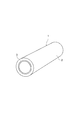
- FIG. 1 is a perspective view of a roll according to an embodiment. As shown in FIG. 1, the roll 1 according to this embodiment is obtained by winding an adhesive tape 2 around a cylindrical core 3 in a plurality of layers.
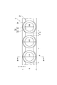
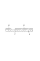
- FIG. 2 is a plan view showing a state in which the adhesive tape is stretched.
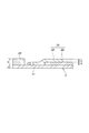
- 3 is a cross-sectional view taken along line III-III shown in FIG.
- the adhesive tape 2 includes a long release film 21, an adhesive layer 24 composed of a first adhesive layer 22 and a second adhesive layer 23, and a support layer 25. And are laminated.
- the first adhesive layer 22 is a layer that functions as a die bonding film. That is, the first adhesive layer 22 is attached to a semiconductor wafer and adheres and fixes a semiconductor chip that has been cut into pieces by dicing to a die pad. For this reason, the first adhesive layer 22 is formed in a circular thin film shape.
- the composition of the adhesive contained in the first adhesive layer 22 is not particularly limited. For example, an epoxy resin, an acrylic resin, a phenol resin, a polyimide resin, a silicon resin, or the like is used. Can do.
- the layer thickness A of the first adhesive layer 22 can be, for example, 1 ⁇ m or more and 250 ⁇ m or less, and preferably 5 ⁇ m or more and 200 ⁇ m or less.
- the diameter ⁇ B of the first adhesive layer 22 is, for example, larger than the diameter of the semiconductor wafer to be diced and smaller than the inner diameter of the wafer ring.
- the inner diameter of the wafer ring is larger than the diameter of the semiconductor wafer to be diced.
- the diameter ⁇ B of the first adhesive layer 22 is preferably 20 mm or more larger than the diameter of the semiconductor wafer to be diced.
- the diameter ⁇ B of the first adhesive layer 22 may be, for example, not less than 300 mm and not more than 350 mm.
- it can be 310 mm or more and 330 mm or less, More preferably, it can be 319 mm or more and 321 mm or less.
- the second adhesive layer 23 is a layer that functions as a dicing tape. That is, the second adhesive layer 23 supports the semiconductor wafer during dicing and bonds and fixes the wafer ring. For this reason, the second adhesive layer 23 is formed in a circular thin film having a larger area than the first adhesive layer 22 that can cover the first adhesive layer 22. Although it does not restrict
- the composition of the adhesive contained in the second adhesive layer 23 may be any as long as it has an adhesive force that does not peel from the wafer ring.
- composition of the adhesive contained in the second adhesive layer 23 examples include chlorinated polypropylene resin, acrylic resin, polyester resin, polyurethane resin, epoxy resin, polyethylene, polypropylene, ethylene-propylene copolymer, polybutene-1, Poly-4-methylpentene-1, ethylene-vinyl acetate copolymer, ethylene-ethyl acrylate copolymer, ethylene-methyl acrylate copolymer, ethylene-acrylic acid copolymer, ionomer, styrene-ethylene-butene
- a pentene copolymer, a polyamide-polyol copolymer, a mixture thereof, or the like can be used.
- the layer thickness C of the second adhesive layer 23 can be, for example, 1 ⁇ m or more and 250 ⁇ m or less, preferably 5 ⁇ m or more and 200 ⁇ m or less.
- the diameter ⁇ D of the second adhesive layer 23 is larger than the inner diameter of the wafer ring. From the viewpoint of securely bonding to the wafer ring, the diameter ⁇ D of the second adhesive layer 23 is preferably sufficiently larger than the inner diameter of the wafer ring.
- the diameter ⁇ D of the second adhesive layer 23 can be, for example, 360 mm or more and 375 mm or less, preferably 365 mm or more and 375 mm or less, and more preferably Can be 369 mm or more and 371 mm or less.
- the adhesive layer 24 includes the first adhesive layer 22 and the second adhesive so that the first adhesive layer 22 is completely covered with the second adhesive layer 23 and is not exposed from the second adhesive layer 23.
- the layer 23 is laminated concentrically. For this reason, the entire surface of the first adhesive layer 22 is adhered to the release film 21, and the peripheral portion of the second adhesive layer 23 surrounds the release film 21 so as to surround the entire outer periphery of the first adhesive layer 22. It is glued.
- the thickness of the peripheral part of the adhesive layer 24 is the thickness C of the second adhesive layer 23, and the thickness of the central part of the adhesive layer 24 is the same as the thickness A of the first adhesive layer 22 and the second thickness A.
- the thickness (A + C) is obtained by adding the thickness C of the adhesive layer 23.
- the radial distance E between the outer edge of the second adhesive layer 23 and the outer edge of the first adhesive layer 22 can be, for example, 30 mm or more, preferably 30 mm or more and 80 mm or less. Preferably, it can be 20 mm or more and 30 mm or less.
- a plurality of adhesive layers 24 configured in this way are formed on the release film 21, and each adhesive layer 24 is in the longitudinal direction of the release film 21 at the center in the short direction of the release film 21. Are arranged at a constant pitch (interval).
- the separation distance F between the adhesive layers 24 adjacent in the longitudinal direction of the release film 21 can be, for example, 0 mm or more and 18 mm or less, preferably 5 mm or more and 15 mm or less, and more preferably 6.5 mm or more. It can be 10.5 mm or less.
- the pitch P of the adhesive layer 24 in the longitudinal direction of the release film 21 is preferably 376.5 mm or more and 379.5 mm or less.
- the pitch P is a value obtained by adding the diameter ⁇ D of the adhesive layer 24 and the separation distance F of the adhesive layer 24 adjacent in the longitudinal direction of the release film 21.
- the support layer 25 reduces the transfer after winding onto the adhesive layer 24 when the adhesive tape 2 is wound around the core 3.
- the support layer 25 is formed so as to surround the periphery of the adhesive layer 24 at a portion other than the central portion in the short direction of the release film 21. Further, the support layer 25 extends continuously or intermittently in the longitudinal direction of the release film 21. Although it does not restrict
- the layer thickness G of the support layer 25 is not particularly limited, but from the viewpoint of suppressing the occurrence of transfer to the adhesive layer 24, it is equal to or greater than the maximum layer thickness (A + C) of the adhesive layer 24. can do.
- the inner diameter ⁇ H of the support layer 25 surrounding the adhesive layer 24 of the support layer 25 is larger than the diameter ⁇ D of the second adhesive layer 23.
- the inner diameter ⁇ H of the support layer 25 can be, for example, 371 mm or more and 385 mm or less, preferably 373 mm or more and 380 mm or less, More preferably, it can be 376 mm or more and 378 mm or less.
- the release film 21 is for adhering and supporting the adhesive layer 24 and winding it around the core 3.
- base materials such as a polyester film, a polypropylene film, a polyethylene terephthalate film, a polyimide film, a polyetherimide film, a polyether naphthalate film, a polymethylpentene film A film can be used.
- These substrate films may be subjected to surface treatment such as primer coating, UV treatment, corona discharge treatment, polishing treatment, and etching treatment as necessary.
- the thickness J of the release film 21 can be, for example, 10 ⁇ m or more and 200 ⁇ m or less, and preferably 20 ⁇ m or more and 150 ⁇ m or less.
- the width K in the short direction of the release film 21 is larger than the diameter ⁇ D of the second adhesive layer 23.
- the width K in the short direction of the release film 21 can be, for example, 380 mm or more and 410 mm or less, preferably 385 mm or more and 400 mm or less. More preferably, it can be 388 mm or more and 392 mm or less.
- the separation distance L between the both edges in the short direction of the release film 21 and the second adhesive layer 23 on a straight line extending in the short direction of the release film 21 through the center of the second adhesive layer 23 is, for example, 5 mm. It can be made 15 mm or less, preferably 7 mm or more and 13 mm or less, more preferably 8 mm or more and 12 mm or less.
- the separation distance L is the shortest distance between the both edges in the short direction of the release film 21 and the second adhesive layer 23.
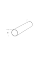
- FIG. 4 is a perspective view of the core according to the embodiment. As shown in FIG. 4, the core 3 is formed in a cylindrical shape.
- the composition of the core 3 is not particularly limited, and for example, a plastic such as PS resin, PE resin, ABS resin can be used.
- the outer diameter M is the outer diameter of the core 3.
- the outer circumferential length O is the circumferential length of the outer circumference of the core 3 and is obtained by the outer circumference M ⁇ ⁇ .
- FIG. 5 is a schematic development view of the adhesive tape wound around the core.
- the left-right direction (arrow direction) is the circumferential direction of the core 3.
- the outer diameter M of the core 3 is at least that of the adhesive tape 2 wound around the core 3 when the adhesive tape 2 is wound around the core 3 in a plurality of layers.
- the displacement amount N of the adhesive layer 24 in the circumferential direction of the core 3 is 55 mm between the inner tape portion 2a and the outer tape portion 2b of the adhesive tape 2 adjacent in the radial direction of the core 3.
- the dimensions are as follows.
- the inner tape portion 2a is a portion disposed adjacent to the inner side (lower layer side) of the outer tape portion 2b in the radial direction of the core 3, and the outer tape portion 2b is arranged in the radial direction of the core 3.
- the outer diameter M of the core 3 is preferably a dimension such that the deviation amount N is 25 mm or less. It is more preferable that N is a dimension of 15 mm or less.
- the pitch P of the adhesive layer 24 is 378 mm.
- the outer peripheral length O of the core 3 is set to 323 mm (378 mm ⁇ 55 mm) or more and 433 mm (378 mm + 55 mm) or less, thereby bonding the core 3 in the circumferential direction.
- the deviation amount N of the agent layer 24 can be 55 mm or less.
- the outer diameter M of the core 3 is set to 323 / ⁇ mm (about 103 mm) or more and 433 / ⁇ mm (about 138 mm) or less, the deviation amount N of the adhesive layer 24 in the circumferential direction of the core 3 is 55 mm. It can be as follows. Note that the outer peripheral length O and the outer diameter M of the core 3 having a plurality of pitches of about one turn can be obtained by simple calculation, and thus the description thereof is omitted here.
- the semiconductor wafer is attached (laminated) to the first adhesive layer 22 disposed in the center of the adhesive layer 24, and the adhesive layer 24.
- a semiconductor wafer is not affixed to the second adhesive layer 23 disposed at the peripheral edge of the semiconductor wafer. Therefore, by setting the outer diameter M and the outer peripheral length O of the winding core 3 in this way, the inner tape portion 2a and the outer tape can be obtained without reducing the winding tension when the adhesive tape 2 is wound around the winding core 3.
- the gap amount N of the adhesive layer 24 in the circumferential direction of the core 3 can be suppressed to 55 mm or less, 25 mm or less, or 15 mm or less between the portion 2 b.
- the radius of the adhesive tape 2 increases. For this reason, when the adhesive tape 2 is long, even if the deviation amount N of the adhesive layer 24 near the core 3 is suppressed to 55 mm or less, 25 mm or less, and 15 mm or less, The amount of deviation N of the adhesive layer 24 may exceed 55 mm, 25 mm, and 15 mm.
- the tension acting on the adhesive tape 2 wound around the core 3 becomes larger toward the inner side in the radial direction, so that the transfer marks are not transferred. Although the problem becomes large, the tension acting on the adhesive tape 2 wound around the core 3 becomes smaller toward the outer side in the radial direction, so that the problem of transfer marks does not occur.
- the displacement amount N of the adhesive layer 24 in the circumferential direction of the core 3 is suppressed to 55 mm or less, 25 mm or less, and 15 mm or less between the inner tape portion 2a and the outer tape portion 2b.
- the outer peripheral length O of the core 3 is (P ⁇ 55) mm or more and (P + 55) mm or less, (P-25) mm or more and (P + 25) mm or less and (P-15) mm or more and (P + 15) mm or less, so that one pitch of the adhesive layer is about 1 turn, and one adhesive layer 24 is formed. It can be wound around the core 3 in about one round. For this reason, the deviation amount N of the adhesive layer 24 can be set to the above-described range between the inner tape portion 2a and the outer tape portion 2b without excessively increasing the outer diameter of the core 3.
- the outer diameter M of the core 3 is the same as that of the inner tape portion 2 a when the adhesive tape 2 is wound around the core 3. It is preferable that the peripheral edge 22a of the first adhesive layer 22 and the peripheral edge 23a of the second adhesive layer 23 do not overlap with the outer tape portion 2b.
- the diameter ⁇ B of the first adhesive layer 22 is 320 mm
- the diameter ⁇ D of the second adhesive layer 23 is 370 mm
- the pitch P of the adhesive layer 24 is 378 mm.
- the separation distance E between the peripheral edge 22a of the first adhesive layer 22 and the peripheral edge 23a of the second adhesive layer 23 in the circumferential direction of the core 3 is 25 mm.
- the outer peripheral length O of the core 3 is larger than 353 mm (378 mm-25 mm) and smaller than 403 mm (378 mm + 25 mm), so that the inner tape portion 2a It is possible to prevent the peripheral edge 22a of the first adhesive layer 22 and the peripheral edge 23a of the second adhesive layer 23 from overlapping with the outer tape portion 2b.
- the outer diameter M of the winding core 3 is set to a dimension larger than 353 / ⁇ mm (about 112 mm) and smaller than 403 / ⁇ (about 128 mm) mm, it is between the inner tape portion 2a and the outer tape portion 2b.
- the peripheral edge 22a of the first adhesive layer 22 and the peripheral edge 23a of the second adhesive layer 23 can be prevented from overlapping each other.
- the outer peripheral length O and the outer diameter M of the core 3 having a plurality of pitches of about one turn can be obtained by simple calculation, and thus the description thereof is omitted here.
- the outer diameter M of the core 3 is preferably 100 mm or more. In this case, it is preferably 140 mm or less, more preferably 130 mm or less, and particularly preferably 120 mm or less.
- the adhesive tape wound around the core 3 can be obtained without reducing the winding tension when the adhesive tape 2 is wound around the core 3.
- the tension acting on 2 can be reduced. Thereby, it is possible to prevent the transfer mark from being generated in the adhesive layer 24 and to prevent the winding deviation of the adhesive tape 2.
- the transportability and storage property of the roll 1 can be improved.
- the adhesive layer 24 ′ may be a single layer.
- the adhesive layer 24 ′ may be, for example, only the first adhesive layer or only the second adhesive layer, and the first adhesive layer and the second adhesive layer are integrated. It may be a single layer. Also by this, the same operation effect as the above-mentioned embodiment can be produced.
- stacked on a release film demonstrated as what laminated
- the first adhesive layer 22 ′′ may be laminated on the second adhesive layer 23 ′′, like the adhesive layer 24 ′′.
- the second adhesive layer 23 ′′ is formed on the base film 21, and the first adhesive layer 22 ′′ has a smaller area than the second adhesive layer 23 ′′ and the second adhesive layer 23 from the outer periphery. "Is exposed on the second adhesive layer 23".
- the outer diameter of the winding core is such that when the adhesive tape 2 "is wound around the winding core, the inner tape portion and the outer tape portion. Between the first adhesive layer 22 ′′ and the second adhesive layer 23 ′′ so that they do not overlap each other. Also by this, the same operation effect as the above-mentioned embodiment can be produced.
- the conditions of the amount of misalignment of an adhesive bond layer, and the conditions of the overlap of the periphery of a 1st adhesive bond layer and the periphery of a 2nd adhesive bond layer are the adhesive tape wound up by the core. Although described as at least the 10th layer, this may be less than the 10th layer of the adhesive tape wound around the core.
- the adhesive tape is described as a dicing / die bonding integrated tape having a first adhesive layer that functions as a die bonding film and a second adhesive layer that functions as a dicing tape.
- each adhesive layer can be appropriately selected according to the purpose of use.
- Example 1 As the adhesive tape, a dicing / die bonding integrated tape manufactured by Hitachi Chemical Co., Ltd. and having a trade name “FH-4013 series” was used. A die bonding film having a diameter of 320 mm and a layer thickness of 135 ⁇ m was formed on the first adhesive layer, and a dicing tape having a diameter of 370 mm and a layer thickness of 120 ⁇ m was formed on the second adhesive layer. . Further, the separation distance between the outer edge of the first adhesive layer and the outer edge of the second adhesive layer was 25 mm, and the pitch of the adhesive layer was 378 mm.
- an ABS resin winding core having an outer diameter of 100 mm and an outer peripheral length of 314 mm was manufactured from ABS resin.
- One pitch of the adhesive layer was set to about 1 roll, and the above-mentioned adhesive tape was wound around the created core to create a roll.
- the winding tension when winding the adhesive tape around the winding core was 18N, 20N, and 22N.
- the adhesive tape wound around the winding core has a gap amount of 42.6 mm or less in the circumferential direction of the winding core between the inner tape portion and the outer tape portion up to at least the 10th layer. .
- Example 2 The conditions were the same as in Example 1 except that the outer diameter of the core was 114 mm.
- the adhesive tape wound around the winding core has an adhesive layer displacement of 1.1 mm or less in the circumferential direction of the winding core between the inner tape portion and the outer tape portion up to at least the 10th layer. .
- Example 3 The conditions were the same as in Example 1 except that the outer diameter of the core was 120 mm.
- the adhesive tape wound around the winding core has a gap of 16.8 mm or less in the circumferential direction of the winding core between the inner tape portion and the outer tape portion up to at least the 10th layer. .
- Example 2 The conditions were the same as in Example 1 except that the outer diameter of the winding core was 84.0 mm. Note that the core having an outer diameter of 84.0 mm is of a size generally used in the market.
- the adhesive tape wound around the winding core has an adhesive layer misalignment of 89.1 mm or less between the inner tape portion and the outer tape portion in the circumferential direction up to at least the 10th layer. .
Landscapes
- Chemical & Material Sciences (AREA)
- Organic Chemistry (AREA)
- Adhesive Tapes (AREA)
- Storage Of Web-Like Or Filamentary Materials (AREA)
- Dicing (AREA)
Description
る。
接着テープには、日立化成工業株式会社製、商品名「FH-4013シリーズ」のダイシング・ダイボンディング一体型テープを用いた。第一接着剤層には、直径が320mm、層厚が135μmのダイボンディングフィルムが形成されており、第二接着剤層には、直径が370mm、層厚が120μmのダイシングテープが形成されていた。また、第一接着剤層の外縁と第二接着剤層の外縁との離間距離が25mm、接着剤層のピッチが378mmであった。
巻芯の外径を114mmとした他は、実施例1と同じ条件とした。
巻芯の外径を120mmとした他は、実施例1と同じ条件とした。
巻芯の外径を84.0mmとした他は、実施例1と同じ条件とした。
なお、外径が84.0mmの巻芯は、市場で一般的に使用されている大きさのものである。

Claims (8)
- 長尺の基材フィルムに接着剤層が前記基材フィルムの長手方向に沿って形成された接着テープを複数層に巻き取る円筒状の巻芯であって、
前記巻芯の外径が、前記巻芯に前記接着テープが巻き取られた際に、前記巻芯の半径方向に隣接する前記接着テープの内側テープ部と外側テープ部との間において、前記巻芯の円周方向における前記接着剤層のズレ量が55mm以下となる寸法である、
巻芯。 - 前記巻芯の外径は、前記巻芯に巻き取られた前記接着テープの少なくとも10層目まで、前記内側テープ部と前記外側テープ部との間において、前記巻芯の円周方向における前記接着剤層のズレ量が55mm以下となる寸法である、
請求項1に記載の巻芯。 - 前記接着テープに形成される前記接着剤層のピッチをPとした場合に、
前記巻芯の外周長は、(P-55)mm以上(P+55)mm以下である、
請求項1又は2に記載の巻芯。 - 前記接着テープの前記接着剤層は、前記基材フィルム上に形成される第一接着剤層と、前記第一接着剤層よりも面積が大きく前記第一接着剤層を覆って前記基材フィルム上に形成される第二接着剤層と、を有し、
前記巻芯の外径は、前記巻芯に前記接着テープが巻き取られた際に、前記内側テープ部と前記外側テープ部との間において、前記第一接着剤層の周縁と前記第二接着剤層の周縁とが重ならない寸法である、
請求項1~3の何れか一項に記載の巻芯。 - 前記接着テープの前記接着剤層は、前記基材フィルム上に形成される第二接着剤層と、前記第二接着剤層よりも面積が小さく外周から前記第二接着剤層が露出するように前記第二接着剤層上に形成される第一接着剤層と、を有し、
前記巻芯の外径は、前記巻芯に前記接着テープが巻き取られた際に、前記内側テープ部と前記外側テープ部との間において、前記第一接着剤層の周縁と前記第二接着剤層の周縁とが重ならない寸法である、
請求項1~3の何れか一項に記載の巻芯。 - 前記巻芯の外径は、前記巻芯に巻き取られた前記接着テープの少なくとも10層目まで、前記内側テープ部と前記外側テープ部との間において、前記第一接着剤層の周縁と前記第二接着剤層の周縁とが重ならない寸法である、
請求項4又は5に記載の巻芯。 - 前記巻芯の外径が、100mm以上である、
請求項1~6の何れか一項に記載の巻芯。 - 長尺の基材フィルムに複数の接着剤層が前記基材フィルムの長手方向に沿って形成された接着テープが円筒状の巻芯に複数層に巻き取られたロールであって、
前記巻芯の外径が、前記巻芯に前記接着テープが巻き取られた際に、前記巻芯の半径方向に隣接する前記接着テープの内側テープ部と外側テープ部との間において、前記接着剤層の前記巻芯の円周方向における重なり長さが55mm以下となる寸法である、
ロール。
Priority Applications (5)
| Application Number | Priority Date | Filing Date | Title |
|---|---|---|---|
| CN201380027215.6A CN104334668B (zh) | 2012-05-25 | 2013-05-24 | 卷材 |
| KR1020197037834A KR102189257B1 (ko) | 2012-05-25 | 2013-05-24 | 권취 코어 및 롤 |
| JP2014516863A JP5935884B2 (ja) | 2012-05-25 | 2013-05-24 | 巻芯及びロール |
| US14/403,588 US10807830B2 (en) | 2012-05-25 | 2013-05-24 | Winding core and roll |
| KR1020147033158A KR102099760B1 (ko) | 2012-05-25 | 2013-05-24 | 권취 코어 및 롤 |
Applications Claiming Priority (2)
| Application Number | Priority Date | Filing Date | Title |
|---|---|---|---|
| JP2012119369 | 2012-05-25 | ||
| JP2012-119369 | 2012-05-25 |
Publications (1)
| Publication Number | Publication Date |
|---|---|
| WO2013176252A1 true WO2013176252A1 (ja) | 2013-11-28 |
Family
ID=49623932
Family Applications (1)
| Application Number | Title | Priority Date | Filing Date |
|---|---|---|---|
| PCT/JP2013/064476 Ceased WO2013176252A1 (ja) | 2012-05-25 | 2013-05-24 | 巻芯及びロール |
Country Status (6)
| Country | Link |
|---|---|
| US (1) | US10807830B2 (ja) |
| JP (1) | JP5935884B2 (ja) |
| KR (2) | KR102099760B1 (ja) |
| CN (1) | CN104334668B (ja) |
| TW (1) | TWI558649B (ja) |
| WO (1) | WO2013176252A1 (ja) |
Cited By (5)
| Publication number | Priority date | Publication date | Assignee | Title |
|---|---|---|---|---|
| JP2016210837A (ja) * | 2015-04-30 | 2016-12-15 | 日東電工株式会社 | 裏面保護フィルム、フィルム、半導体装置の製造方法および保護チップの製造方法 |
| JPWO2015178369A1 (ja) * | 2014-05-23 | 2017-04-20 | 日立化成株式会社 | ダイボンドダイシングシート |
| JP2017123488A (ja) * | 2017-03-17 | 2017-07-13 | 日東電工株式会社 | 半導体装置用フィルム、及び、半導体装置の製造方法 |
| JP2018148218A (ja) * | 2018-04-18 | 2018-09-20 | 日東電工株式会社 | 半導体装置用フィルム、及び、半導体装置の製造方法 |
| JP2019125666A (ja) * | 2018-01-16 | 2019-07-25 | 日立化成株式会社 | 接着シートロール及びその製造方法、並びに、半導体装置の製造方法 |
Families Citing this family (5)
| Publication number | Priority date | Publication date | Assignee | Title |
|---|---|---|---|---|
| KR102212449B1 (ko) * | 2017-05-22 | 2021-02-03 | 주식회사 엘지화학 | 배터리 모듈 및 이를 포함하는 배터리 팩 |
| KR20190037870A (ko) | 2017-09-29 | 2019-04-08 | 에스케이이노베이션 주식회사 | 권취롤 |
| JP6853956B2 (ja) * | 2017-10-06 | 2021-04-07 | ブラザー工業株式会社 | テープロール、テープカートリッジ、及びテープロールの製造方法 |
| CN109575829B (zh) * | 2017-12-29 | 2021-05-07 | 宁波大榭开发区综研化学有限公司 | 一种段差多层复合膜和卷材及其制备方法 |
| CN109179016B (zh) * | 2018-08-09 | 2020-04-21 | 业成科技(成都)有限公司 | 卷材及其制备方法 |
Citations (7)
| Publication number | Priority date | Publication date | Assignee | Title |
|---|---|---|---|---|
| JP2006082953A (ja) * | 2004-09-17 | 2006-03-30 | Showa Marutsutsu Co Ltd | 巻芯およびロール状物 |
| JP2010163577A (ja) * | 2009-01-19 | 2010-07-29 | Furukawa Electric Co Ltd:The | 巻き芯及び巻き芯に巻き付けられたウエハ加工用テープ |
| JP2010177401A (ja) * | 2009-01-29 | 2010-08-12 | Furukawa Electric Co Ltd:The | ウエハ加工用テープ |
| JP2010192856A (ja) * | 2009-02-20 | 2010-09-02 | Furukawa Electric Co Ltd:The | ウエハ加工用フィルム |
| JP2011187595A (ja) * | 2010-03-08 | 2011-09-22 | Furukawa Electric Co Ltd:The | ウエハ加工用テープの長尺体 |
| JP2011201634A (ja) * | 2010-03-25 | 2011-10-13 | Maxell Sliontec Ltd | ロール状物の段差痕低減構造及びロール状物の製造方法 |
| JP2012049474A (ja) * | 2010-08-30 | 2012-03-08 | Hitachi Chem Co Ltd | ウェハ加工用テープ |
Family Cites Families (4)
| Publication number | Priority date | Publication date | Assignee | Title |
|---|---|---|---|---|
| JP4677758B2 (ja) * | 2004-10-14 | 2011-04-27 | 日立化成工業株式会社 | ダイボンドダイシングシート及びその製造方法、並びに、半導体装置の製造方法 |
| JP4876451B2 (ja) | 2005-06-27 | 2012-02-15 | 日立化成工業株式会社 | 接着シート |
| JP5322609B2 (ja) * | 2008-12-01 | 2013-10-23 | 日東電工株式会社 | 半導体装置製造用フィルムロール |
| CN101486850A (zh) * | 2009-02-09 | 2009-07-22 | 屠尖兵 | 一种双面胶带及其生产方法 |
-
2013
- 2013-05-24 US US14/403,588 patent/US10807830B2/en active Active
- 2013-05-24 WO PCT/JP2013/064476 patent/WO2013176252A1/ja not_active Ceased
- 2013-05-24 KR KR1020147033158A patent/KR102099760B1/ko active Active
- 2013-05-24 CN CN201380027215.6A patent/CN104334668B/zh active Active
- 2013-05-24 TW TW102118454A patent/TWI558649B/zh active
- 2013-05-24 JP JP2014516863A patent/JP5935884B2/ja active Active
- 2013-05-24 KR KR1020197037834A patent/KR102189257B1/ko active Active
Patent Citations (7)
| Publication number | Priority date | Publication date | Assignee | Title |
|---|---|---|---|---|
| JP2006082953A (ja) * | 2004-09-17 | 2006-03-30 | Showa Marutsutsu Co Ltd | 巻芯およびロール状物 |
| JP2010163577A (ja) * | 2009-01-19 | 2010-07-29 | Furukawa Electric Co Ltd:The | 巻き芯及び巻き芯に巻き付けられたウエハ加工用テープ |
| JP2010177401A (ja) * | 2009-01-29 | 2010-08-12 | Furukawa Electric Co Ltd:The | ウエハ加工用テープ |
| JP2010192856A (ja) * | 2009-02-20 | 2010-09-02 | Furukawa Electric Co Ltd:The | ウエハ加工用フィルム |
| JP2011187595A (ja) * | 2010-03-08 | 2011-09-22 | Furukawa Electric Co Ltd:The | ウエハ加工用テープの長尺体 |
| JP2011201634A (ja) * | 2010-03-25 | 2011-10-13 | Maxell Sliontec Ltd | ロール状物の段差痕低減構造及びロール状物の製造方法 |
| JP2012049474A (ja) * | 2010-08-30 | 2012-03-08 | Hitachi Chem Co Ltd | ウェハ加工用テープ |
Cited By (7)
| Publication number | Priority date | Publication date | Assignee | Title |
|---|---|---|---|---|
| JPWO2015178369A1 (ja) * | 2014-05-23 | 2017-04-20 | 日立化成株式会社 | ダイボンドダイシングシート |
| TWI697374B (zh) * | 2014-05-23 | 2020-07-01 | 日商日立化成股份有限公司 | 半導體裝置的製造方法 |
| JP2016210837A (ja) * | 2015-04-30 | 2016-12-15 | 日東電工株式会社 | 裏面保護フィルム、フィルム、半導体装置の製造方法および保護チップの製造方法 |
| JP2017123488A (ja) * | 2017-03-17 | 2017-07-13 | 日東電工株式会社 | 半導体装置用フィルム、及び、半導体装置の製造方法 |
| JP2019125666A (ja) * | 2018-01-16 | 2019-07-25 | 日立化成株式会社 | 接着シートロール及びその製造方法、並びに、半導体装置の製造方法 |
| JP7067073B2 (ja) | 2018-01-16 | 2022-05-16 | 昭和電工マテリアルズ株式会社 | 接着シートロール及びその製造方法、並びに、半導体装置の製造方法 |
| JP2018148218A (ja) * | 2018-04-18 | 2018-09-20 | 日東電工株式会社 | 半導体装置用フィルム、及び、半導体装置の製造方法 |
Also Published As
| Publication number | Publication date |
|---|---|
| KR102099760B1 (ko) | 2020-04-10 |
| CN104334668A (zh) | 2015-02-04 |
| US10807830B2 (en) | 2020-10-20 |
| KR20190143488A (ko) | 2019-12-30 |
| JPWO2013176252A1 (ja) | 2016-01-14 |
| KR102189257B1 (ko) | 2020-12-11 |
| TWI558649B (zh) | 2016-11-21 |
| TW201410578A (zh) | 2014-03-16 |
| KR20150018797A (ko) | 2015-02-24 |
| CN104334668B (zh) | 2019-08-06 |
| US20150129706A1 (en) | 2015-05-14 |
| JP5935884B2 (ja) | 2016-06-15 |
Similar Documents
| Publication | Publication Date | Title |
|---|---|---|
| JP5935884B2 (ja) | 巻芯及びロール | |
| CN1327500C (zh) | 切割带贴合单元和具有切割带贴合单元的序列式系统 | |
| CN103155109B (zh) | 晶圆加工用胶带、晶圆加工用胶带的制造方法以及半导体装置的制造方法 | |
| KR101422603B1 (ko) | 접착 시트 | |
| TWI452619B (zh) | Wafer processing film | |
| JP2008311514A (ja) | 半導体ウエハの研削方法および表面保護用シート | |
| CN102349134A (zh) | 晶片加工用薄膜以及使用晶片加工用薄膜制造半导体装置的方法 | |
| JP2013125925A (ja) | ウエハ加工用テープ、ウエハ加工用テープの製造方法および回転打抜き刃 | |
| JP5438522B2 (ja) | ダイシング−ダイボンディングテープ及びその製造方法 | |
| JP6170678B2 (ja) | 半導体ウエハ加工用シートおよびその製造方法 | |
| JP4999111B2 (ja) | ウエハ加工用テープ | |
| JP4785080B2 (ja) | ウエハ加工用テープ | |
| TWI600069B (zh) | 晶圓加工用膠帶 | |
| TW201922513A (zh) | 半導體裝置製造用接著膜及其製造方法以及半導體裝置及其製造方法 | |
| JP5435474B2 (ja) | ウエハ加工用テープ体 | |
| JP2014135336A (ja) | 半導体ウエハ加工用シートおよびその製造方法 | |
| JP2024034201A (ja) | 積層フィルム巻回体 | |
| KR20250104852A (ko) | 반도체 장치용 접착시트 | |
| CN105694748A (zh) | 晶片加工用带 | |
| JP2025007655A (ja) | 積層フィルム及び半導体装置の製造方法 | |
| JP6452416B2 (ja) | ウエハ加工用テープ | |
| WO2024219099A1 (ja) | 接着フィルム及び接着フィルムの製造方法 | |
| JP2016111160A (ja) | ウエハ加工用テープ |
Legal Events
| Date | Code | Title | Description |
|---|---|---|---|
| 121 | Ep: the epo has been informed by wipo that ep was designated in this application |
Ref document number: 13794318 Country of ref document: EP Kind code of ref document: A1 |
|
| ENP | Entry into the national phase |
Ref document number: 2014516863 Country of ref document: JP Kind code of ref document: A |
|
| NENP | Non-entry into the national phase |
Ref country code: DE |
|
| WWE | Wipo information: entry into national phase |
Ref document number: 14403588 Country of ref document: US |
|
| ENP | Entry into the national phase |
Ref document number: 20147033158 Country of ref document: KR Kind code of ref document: A |
|
| 122 | Ep: pct application non-entry in european phase |
Ref document number: 13794318 Country of ref document: EP Kind code of ref document: A1 |