WO2013161685A1 - 表示装置 - Google Patents
表示装置 Download PDFInfo
- Publication number
- WO2013161685A1 WO2013161685A1 PCT/JP2013/061579 JP2013061579W WO2013161685A1 WO 2013161685 A1 WO2013161685 A1 WO 2013161685A1 JP 2013061579 W JP2013061579 W JP 2013061579W WO 2013161685 A1 WO2013161685 A1 WO 2013161685A1
- Authority
- WO
- WIPO (PCT)
- Prior art keywords
- drive circuit
- driver
- connection wiring
- input terminal
- display
- Prior art date
- Legal status (The legal status is an assumption and is not a legal conclusion. Google has not performed a legal analysis and makes no representation as to the accuracy of the status listed.)
- Ceased
Links
Images






Classifications
-
- G—PHYSICS
- G02—OPTICS
- G02F—OPTICAL DEVICES OR ARRANGEMENTS FOR THE CONTROL OF LIGHT BY MODIFICATION OF THE OPTICAL PROPERTIES OF THE MEDIA OF THE ELEMENTS INVOLVED THEREIN; NON-LINEAR OPTICS; FREQUENCY-CHANGING OF LIGHT; OPTICAL LOGIC ELEMENTS; OPTICAL ANALOGUE/DIGITAL CONVERTERS
- G02F1/00—Devices or arrangements for the control of the intensity, colour, phase, polarisation or direction of light arriving from an independent light source, e.g. switching, gating or modulating; Non-linear optics
- G02F1/01—Devices or arrangements for the control of the intensity, colour, phase, polarisation or direction of light arriving from an independent light source, e.g. switching, gating or modulating; Non-linear optics for the control of the intensity, phase, polarisation or colour
- G02F1/13—Devices or arrangements for the control of the intensity, colour, phase, polarisation or direction of light arriving from an independent light source, e.g. switching, gating or modulating; Non-linear optics for the control of the intensity, phase, polarisation or colour based on liquid crystals, e.g. single liquid crystal display cells
- G02F1/133—Constructional arrangements; Operation of liquid crystal cells; Circuit arrangements
- G02F1/13306—Circuit arrangements or driving methods for the control of single liquid crystal cells
-
- G—PHYSICS
- G02—OPTICS
- G02F—OPTICAL DEVICES OR ARRANGEMENTS FOR THE CONTROL OF LIGHT BY MODIFICATION OF THE OPTICAL PROPERTIES OF THE MEDIA OF THE ELEMENTS INVOLVED THEREIN; NON-LINEAR OPTICS; FREQUENCY-CHANGING OF LIGHT; OPTICAL LOGIC ELEMENTS; OPTICAL ANALOGUE/DIGITAL CONVERTERS
- G02F1/00—Devices or arrangements for the control of the intensity, colour, phase, polarisation or direction of light arriving from an independent light source, e.g. switching, gating or modulating; Non-linear optics
- G02F1/01—Devices or arrangements for the control of the intensity, colour, phase, polarisation or direction of light arriving from an independent light source, e.g. switching, gating or modulating; Non-linear optics for the control of the intensity, phase, polarisation or colour
- G02F1/13—Devices or arrangements for the control of the intensity, colour, phase, polarisation or direction of light arriving from an independent light source, e.g. switching, gating or modulating; Non-linear optics for the control of the intensity, phase, polarisation or colour based on liquid crystals, e.g. single liquid crystal display cells
- G02F1/133—Constructional arrangements; Operation of liquid crystal cells; Circuit arrangements
- G02F1/1333—Constructional arrangements; Manufacturing methods
- G02F1/1345—Conductors connecting electrodes to cell terminals
- G02F1/13452—Conductors connecting driver circuitry and terminals of panels
-
- G—PHYSICS
- G02—OPTICS
- G02F—OPTICAL DEVICES OR ARRANGEMENTS FOR THE CONTROL OF LIGHT BY MODIFICATION OF THE OPTICAL PROPERTIES OF THE MEDIA OF THE ELEMENTS INVOLVED THEREIN; NON-LINEAR OPTICS; FREQUENCY-CHANGING OF LIGHT; OPTICAL LOGIC ELEMENTS; OPTICAL ANALOGUE/DIGITAL CONVERTERS
- G02F1/00—Devices or arrangements for the control of the intensity, colour, phase, polarisation or direction of light arriving from an independent light source, e.g. switching, gating or modulating; Non-linear optics
- G02F1/01—Devices or arrangements for the control of the intensity, colour, phase, polarisation or direction of light arriving from an independent light source, e.g. switching, gating or modulating; Non-linear optics for the control of the intensity, phase, polarisation or colour
- G02F1/13—Devices or arrangements for the control of the intensity, colour, phase, polarisation or direction of light arriving from an independent light source, e.g. switching, gating or modulating; Non-linear optics for the control of the intensity, phase, polarisation or colour based on liquid crystals, e.g. single liquid crystal display cells
- G02F1/133—Constructional arrangements; Operation of liquid crystal cells; Circuit arrangements
- G02F1/1333—Constructional arrangements; Manufacturing methods
- G02F1/133345—Insulating layers
-
- G—PHYSICS
- G02—OPTICS
- G02F—OPTICAL DEVICES OR ARRANGEMENTS FOR THE CONTROL OF LIGHT BY MODIFICATION OF THE OPTICAL PROPERTIES OF THE MEDIA OF THE ELEMENTS INVOLVED THEREIN; NON-LINEAR OPTICS; FREQUENCY-CHANGING OF LIGHT; OPTICAL LOGIC ELEMENTS; OPTICAL ANALOGUE/DIGITAL CONVERTERS
- G02F1/00—Devices or arrangements for the control of the intensity, colour, phase, polarisation or direction of light arriving from an independent light source, e.g. switching, gating or modulating; Non-linear optics
- G02F1/01—Devices or arrangements for the control of the intensity, colour, phase, polarisation or direction of light arriving from an independent light source, e.g. switching, gating or modulating; Non-linear optics for the control of the intensity, phase, polarisation or colour
- G02F1/13—Devices or arrangements for the control of the intensity, colour, phase, polarisation or direction of light arriving from an independent light source, e.g. switching, gating or modulating; Non-linear optics for the control of the intensity, phase, polarisation or colour based on liquid crystals, e.g. single liquid crystal display cells
- G02F1/133—Constructional arrangements; Operation of liquid crystal cells; Circuit arrangements
- G02F1/1333—Constructional arrangements; Manufacturing methods
- G02F1/1335—Structural association of cells with optical devices, e.g. polarisers or reflectors
- G02F1/1336—Illuminating devices
- G02F1/133602—Direct backlight
Definitions
- the present invention relates to a display device.
- Display devices including a display panel such as a liquid crystal panel are used for portable information terminal devices such as mobile phones, smartphones, and tablet laptop computers, and electronic devices such as computers.
- a display device includes a display panel having a display unit for displaying an image, and an LSI for driving the display panel by supplying an output signal generated by processing an input signal supplied from a signal supply source to the display unit.
- COG Chip On Glass
- the other end side of the flexible substrate whose one end side is connected to the external signal supply source is attached to the non-display portion of the display panel, and from the external signal supply source transmitted by the flexible substrate.
- a signal is supplied to the driver via connection wiring provided in a non-display portion of the display panel.
- a plurality of drivers may be used depending on the screen size and definition (resolution) of the display panel, but in that case, there may be a problem in securing the installation space for the connection wiring.
- the connection wiring that connects the relatively far driver and the flexible board may have a longer wiring length and higher wiring resistance than the connection wiring that connects the relatively closer driver and the flexible board. Because of concern, it may be preferable to relatively widen the wiring width.
- the present invention has been completed based on the above situation, and aims to keep the non-display portion small.
- the display device of the present invention is attached to the non-display portion of the display panel having a display portion capable of displaying an image and a non-display portion outside the display portion, and is connected to an external signal supply source.
- An external connection member and an output signal attached to the non-display portion of the display panel and generated by processing an input signal supplied from the external signal supply source via the external connection member is output to the display portion
- the input signal from the external signal supply source is supplied to the plurality of drive circuit units via the external connection member and the plurality of connection wirings.
- the plurality of driving circuit units can process the supplied input signal to generate an output signal, and output the output signal to the display unit, thereby driving the display panel.
- the arrangement space of the connection wiring in the non-display portion becomes wider.
- the plurality of connection wirings connect the second drive circuit portion and the external connection member relatively far from the external connection member, and at least part of the first drive circuit portion is relatively close to the external connection member. Since the overlapping connection wiring arranged so as to overlap with the first driving circuit portion is included, the second driving circuit portion and the external connection member are connected in the non-display portion as much as the overlapping connection wiring overlaps with the first driving circuit portion. In addition, it is possible to secure a wide arrangement space for non-overlapping connection wiring that is non-overlapping with respect to the first drive circuit unit.
- the wiring resistance is equalized in the connection wiring that connects the first drive circuit unit and the external connection member and the connection wiring that connects the second drive circuit unit and the external connection member Can be achieved.
- the non-display portion is kept small, which is suitable for reducing the outer shape of the display device and narrowing the frame.
- the plurality of connection wirings include a first connection wiring that connects the first drive circuit unit and the external connection member, and a second connection that connects the second drive circuit unit and the external connection member.
- the second connection wiring includes the superimposed connection wiring and the non-overlapping connection wiring, and the second connection wiring is wider than the first connection wiring. It is formed to become.
- the wiring resistance can be equalized between the first connection wiring having a relatively short wiring length and the second connection wiring having a relatively long wiring length. This makes it difficult for the input signals supplied to the first drive circuit unit and the second drive circuit unit via the first connection wiring and the second connection wiring to become dull.
- the cost required for providing the first connection wiring and the second connection wiring Can be kept low.
- the external connection member is arranged in such a manner that an attachment site for the display panel extends along an end portion of the display panel, the plurality of drive circuit units are arranged on the display panel. Arranged intermittently along the edge. In this way, since the plurality of drive circuit units are intermittently arranged along the end of the display panel, that is, the direction in which the external connection member extends, the second drive circuit unit is connected to the first drive circuit unit. Compared to the external connection member, it is disposed further away. Even in such a case, by including the superimposed connection wiring in the connection wiring as described above, the second drive circuit unit and the external connection member in the non-display portion are equivalent to the overlap of the superimposed connection wiring with the first drive circuit unit. It is possible to secure a wide space for disposing the non-overlapping connection wirings, and to keep the non-display portion small.
- the first drive circuit unit is arranged at a position overlapping the external connection member in a direction along the end of the display panel, whereas the second drive circuit unit is arranged at an end of the display panel. It arrange
- the connection wiring that connects the second drive circuit unit and the external connection member is more complicated in wiring shape than the connection wiring that connects the first drive circuit unit and the external connection member. It becomes more difficult to secure the arrangement space.
- the second drive circuit unit and the external connection member are connected in the non-display portion by the amount that the superimposed connection wiring is superimposed on the first drive circuit unit. Therefore, it is possible to secure a wide arrangement space for the non-overlapping connection wiring, and thus to keep the non-display portion small.
- the first drive circuit unit is disposed near the center of the end portion of the display panel, whereas the second drive circuit unit is disposed near the end of the end portion of the display panel.
- the external connection member is disposed at a central portion at the end of the display panel.
- the one disposed near the end of the display panel is the second drive circuit unit that is connected to the external connection member by the overlapping connection wiring. It can be set as the arrangement
- the first drive circuit unit is arranged in a pair near the center of the end of the display panel, whereas the second drive circuit unit is a pair near the both ends of the end of the display panel. Is arranged. In this way, even when at least four drive circuit units are arranged side by side, the pair of second drive circuit units arranged near both ends are connected to the external connection member by the overlapping connection wiring, respectively. In addition, it is possible to secure a wide arrangement space for the non-overlapping connection wirings that connect the pair of second drive circuit units to the external connection member, respectively, so that the non-display unit can be kept small.
- An insulating layer is formed on the overlapping connection wiring so as to be laminated on the overlapping first driving circuit portion side. In this way, it is possible to prevent a situation in which the overlapping connection wiring is erroneously connected to the first drive circuit unit by the insulating layer.
- the first wiring circuit is connected to the third driving circuit unit and the external connection member, and at least a part of the third driving circuit unit is arranged to overlap the first driving circuit unit and the second driving circuit unit. 2 overlapping connection wirings.
- the connection wiring that connects the second drive circuit unit and the external connection member includes the overlapping connection wiring that overlaps the first drive circuit unit, and the third drive circuit unit and the external connection member.
- connection wiring for connecting the first drive circuit unit and the second drive circuit unit includes a second superimposed connection wiring that overlaps the first drive circuit unit and the second drive circuit unit.
- a wide arrangement space for the wiring and the second non-overlapping connection wiring for connecting the third drive circuit unit and the external connection member can be secured.
- the non-display portion of the display panel is provided with an input terminal portion
- the first drive circuit portion includes a circuit side input terminal portion connected to the input terminal portion
- the non-display unit of the display panel is connected to a superimposition unit of the superimposition connection wiring with the first drive circuit unit.
- the first drive circuit unit is provided with a circuit-side dummy terminal unit that is connected to the dummy terminal unit but is not connected to the processing circuit unit. According to this configuration, in addition to connecting the input terminal portion on the display panel side to the circuit side input terminal portion on the first drive circuit portion side, the dummy terminals connected to the superimposed connection wiring on the display panel side are first connected.
- connection state of the input terminal portion and the circuit side input terminal portion can be stabilized.
- the superimposed connection wiring is connected to the circuit side dummy terminal portion, but not connected to the processing circuit portion, the input signal supplied to the superimposed connection wiring is erroneously processed in the first drive circuit portion. Can be prevented.
- the non-display portion of the display panel has a first input terminal portion connected to the first drive circuit portion, and is connected to the first drive circuit portion and more than the first input terminal portion.
- a plurality of first output terminal portions arranged at positions near the display portion are provided, and the overlapping connection wiring is provided between the plurality of first input terminal portions, the first input terminal portions, and the first input terminal portions.
- the second drive circuit unit is connected to at least one of the first output terminal unit and the first output terminal unit. If it does in this way, the superimposition connection wiring which overlaps with the 1st drive circuit part will have at least any one between a plurality of 1st input terminal parts, and between the 1st input terminal parts and the 1st output terminal parts.
- the superimposed connection is assumed to be a path that passes between the plurality of first output terminal sections. A hand necessary for preventing the wiring from being short-circuited to the first output terminal is not necessary. Thereby, the manufacturing cost of a display panel can be suppressed low.
- the non-display portion of the display panel includes a second input terminal portion connected to the second drive circuit portion and a second input terminal portion connected to the second drive circuit portion and more than the second input terminal portion.
- a plurality of second output terminal portions arranged at positions near the display portion are provided, and the overlapping connection wiring is provided between the plurality of first input terminal portions, the first input terminal portions, and the It is connected to the second input terminal portion through between the first output terminal portions and between the second input terminal portion and the second output terminal portion. If it does in this way, compared with the case where a superimposition connection wiring is connected from the opposite side to the 2nd output terminal part side to the 2nd input terminal part, the 2nd output terminal part will be compared with the 2nd input terminal part.
- a large space can be secured there by the amount that the overlapping connection wiring is not arranged on the side opposite to the side. As a result, it is possible to secure a wider space for disposing the non-overlapping connection wiring, thereby keeping the non-display portion small.
- connection wiring is connected to the second drive circuit unit by passing twice between the first input terminal unit and the first output terminal unit. This is suitable when it is difficult to secure a space for passing the overlapping connection wiring between the plurality of first input terminal portions.
- the superimposed connection wiring is connected to the second drive circuit unit through the plurality of first input terminal units twice. If it does in this way, it will become suitable when it is difficult to secure the space which lets an overlap connection wiring pass between the 1st input terminal part and the 1st output terminal part.
- a liquid crystal panel can be exemplified.
- Such a display device can be applied as a liquid crystal display device to various electronic devices such as a portable information terminal, a mobile phone, a notebook computer, and a portable game machine.
- An illuminating device that is opposed to the liquid crystal panel and is disposed on the side opposite to the display side and capable of supplying light to the liquid crystal panel is provided. If it does in this way, an image can be displayed on the display part of a liquid crystal panel using the light supplied from an illuminating device.
- the non-display portion can be kept small.
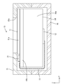
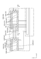
- FIG. 1 is a schematic plan view showing a connection configuration of a liquid crystal panel, a flexible substrate, and a control circuit board on which a driver according to Embodiment 1 of the present invention is mounted.
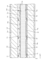
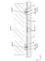
- Sectional drawing which shows the cross-sectional structure along the long side direction of a liquid crystal display device Cross section of liquid crystal panel
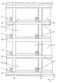
- An enlarged plan view showing a planar configuration of an array substrate constituting a liquid crystal panel
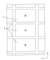
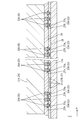
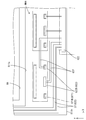
- An enlarged plan view showing a planar configuration of a CF substrate constituting a liquid crystal panel The enlarged plan view which shows the mounting area of the driver and flexible substrate in the array substrate which comprises a liquid crystal panel Vii-vii sectional view of FIG. Viii-viii sectional view of FIG.
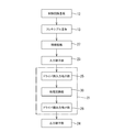
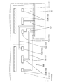
- Block diagram showing signal transmission path Schematic top view which shows the connection structure of the liquid crystal panel which mounted the driver which concerns on Embodiment 2 of this invention, a flexible substrate, and a control circuit board.
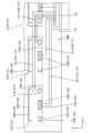
- Enlarged plan view showing mounting area of driver and flexible board on array board The enlarged plan view which shows the mounting area
- FIGS. 1 A first embodiment of the present invention will be described with reference to FIGS.
- the liquid crystal display device 10 is illustrated.
- a part of each drawing shows an X axis, a Y axis, and a Z axis, and each axis direction is drawn to be a direction shown in each drawing.
- FIG. 2 and the like are used as a reference, and the upper side of the figure is the front side and the lower side of the figure is the back side.
- the liquid crystal display device 10 includes a liquid crystal panel (display panel, display element) 11 having a display unit AA capable of displaying an image and a non-display unit NAA outside the display unit AA, and a liquid crystal panel.
- a driver (driving circuit unit) 21 that drives 11, a control circuit board (external power source, external signal supply source) 12 that supplies driving power, reference potential, and input signals related to images to the driver 21 from the outside,
- a flexible substrate (external connection component) 13 that electrically connects the liquid crystal panel 11 and the external control circuit board 12, and a backlight device (illumination device) 14 that is an external light source that supplies light to the liquid crystal panel 11.
- the liquid crystal display device 10 also includes a pair of front and back exterior members 15 and 16 for housing and holding the liquid crystal panel 11 and the backlight device 14 assembled to each other. An opening 15a for exposing the display portion AA of the liquid crystal panel 11 to the outside is formed.
- the liquid crystal display device 10 includes a portable information terminal (including an electronic book and a PDA), a mobile phone (including a smartphone), a notebook computer (including a tablet notebook computer), a digital photo frame, It is used for various electronic devices (not shown) such as portable game machines. For this reason, the screen size of the liquid crystal panel 11 constituting the liquid crystal display device 10 is set to about several inches to several tens of inches, and is generally classified into a small size and a small size.
- the backlight device 14 includes a chassis 14a having a substantially box shape that opens toward the front side (the liquid crystal panel 11 side), and a light source (not shown) such as a cold cathode tube or the like disposed in the chassis 14a. LED, etc.) and an optical member (not shown) arranged to cover the opening of the chassis 14a.
- the optical member has a function of converting light emitted from the light source into a planar shape.
- the liquid crystal panel 11 has a horizontally long rectangular shape (rectangular shape) as a whole, on one end side in the short side direction (upper side in FIG. 1) and in the long side direction.
- the display part (active area) AA is arranged at a position offset to one end side (left side shown in FIG. 1), and offset to the other end side (lower side shown in FIG. 1) in the short side direction.
- the driver 21 and the flexible substrate 13 are respectively attached to the positions.
- a frame-like solid line that is slightly smaller than the CF substrate 11a represents the outer shape of the display portion AA, and a region outside the solid line is a non-display portion NAA.
- an area outside the display area AA is a non-display area (non-active area) NAA in which no image is displayed.
- the non-display area NAA is a substantially frame-shaped area (CF described later) surrounding the display area AA.
- the long side direction in the liquid crystal panel 11 matches the X-axis direction of each drawing, and the short side direction matches the Y-axis direction of each drawing.
- the liquid crystal panel 11 is interposed between a pair of transparent (translucent) glass substrates 11 a and 11 b and both the substrates 11 a and 11 b, and has an optical characteristic as the electric field is applied. And a liquid crystal layer 11c containing liquid crystal molecules as a changing substance, and both substrates 11a and 11b are bonded together with a sealant (not shown) while maintaining a gap corresponding to the thickness of the liquid crystal layer 11c.
- the front side front side
- the back side back side
- the array substrate 11b is the array substrate 11b.
- the CF substrate 11a has a longer side dimension smaller than that of the array substrate 11b, and one in the short side direction with respect to the array substrate 11b (see FIG. 1).
- the upper end shown in FIG. 1 and one end (left side shown in FIG. 1) in the long side direction are bonded together. Therefore, the end of the other side (lower side shown in FIG. 1) of the array substrate 11b in the short side direction and the other side (right side shown in FIG. 1) of the long side direction are arranged on the CF substrate 11a over a predetermined range.
- both the front and back plate surfaces are exposed to the outside without overlapping, and a mounting area for the driver 21 and the flexible board 13 (arrangement area for each of the terminal portions 22 to 24), which will be described later, is secured here.
- alignment films 11d and 11e for aligning liquid crystal molecules contained in the liquid crystal layer are formed on the inner surfaces of both the substrates 11a and 11b, respectively.
- polarizing plates 11f and 11g are attached to the outer surface sides of both the substrates 11a and 11b, respectively.
- the configuration existing in the display unit AA in the array substrate 11b and the CF substrate 11a will be sequentially described in detail.
- the array substrate 11b On the inner surface side of the array substrate 11b (the liquid crystal layer side, the surface facing the CF substrate 11a), as shown in FIGS. 3 and 4, there are many TFTs (Thin Film Transistors) 17 and pixel electrodes 18 which are switching elements.
- the gate wirings 19 and the source wirings 20 are arranged so as to surround the TFTs 17 and the pixel electrodes 18.
- the gate wiring 19 and the source wiring 20 are each made of a metal material (conductive material), and are arranged in such a manner that an insulating layer is interposed between the intersecting portions.
- the gate wiring 19 and the source wiring 20 are connected to the gate electrode and the source electrode of the TFT 17, respectively, and the pixel electrode 18 is connected to the drain electrode of the TFT 17.
- the pixel electrode 18 has a vertically long rectangular shape (rectangular shape) when seen in a plan view, and is made of a transparent electrode material such as ITO (IndiumInTin Oxide) or ZnO (Zinc Oxide).
- the array substrate 11b may be provided with a capacitor wiring (not shown) that is parallel to the gate wiring 19 and overlaps with the insulating layer while traversing the pixel electrode 18.
- the CF substrate 11 a has colored portions such as R (red), G (green), B (blue), etc., in a plane with each pixel electrode 18 on the array substrate 11 b side.
- a large number of color filters 11h are arranged in parallel so as to overlap each other.
- a substantially lattice-shaped light shielding layer (black matrix) 11i for preventing color mixture is formed between each colored portion constituting the color filter 11h.
- the light shielding layer 11i is arranged so as to overlap the above-described gate wiring 19 and source wiring 20 in a plan view.
- a solid counter electrode 11j facing the pixel electrode 18 on the array substrate 11b side is provided on the surface of the color filter 11h and the light shielding layer 11i.
- control circuit board 12 is attached to the back surface of the chassis 14a in the backlight device 14 (the outer surface opposite to the liquid crystal panel 11 side) with screws or the like.
- the control circuit board 12 is a paper phenol or glass epoxy resin board, a power supply part that supplies driving power and a reference potential to the driver 21, and an electronic part that controls transmission of an input signal relating to an image to the liquid crystal panel 11. (Control circuit) is mounted, and wiring (conducting path) having a predetermined pattern (not shown) is routed.
- One end (one end side) of the flexible substrate 13 is electrically and mechanically connected to the control circuit board 12 via an ACF (Anisotropic Conductive Film) (not shown).
- the flexible substrate (FPC substrate) 13 includes a base material made of a synthetic resin material (for example, polyimide resin) having insulating properties and flexibility, and a large number of wirings are provided on the base material. It has a pattern (not shown), and one end in the length direction is connected to the control circuit board 12 arranged on the back side of the chassis 14a as described above, while the other end Since the portion (the other end side) is connected to the array substrate 11 b in the liquid crystal panel 11, the liquid crystal display device 10 is bent in a folded shape so that the cross-sectional shape is substantially U-shaped.
- a synthetic resin material for example, polyimide resin
- the wiring pattern is exposed to the outside to form terminal portions (not shown), and these terminal portions are respectively connected to the control circuit substrate 12 and the array substrate 11b. Are electrically connected to each other. Thereby, it is possible to transmit the driving power, the reference potential, and the input signal related to the image supplied from the control circuit board 12 side to the liquid crystal panel 11 side (see FIG. 9).
- the driver 21 is composed of an LSI chip having a drive circuit 21a therein, and operates based on drive power and a reference potential supplied from the control circuit board 12 as a power source.
- An input signal relating to an image supplied from the control circuit board 12 which is a signal supply source is processed to generate an output signal, and the output signal is output to the display unit AA of the liquid crystal panel 11 (FIG. 9). See).
- the driver 21 has a horizontally long rectangular shape in a plan view and is directly mounted on the non-display portion NAA of the array substrate 11b of the liquid crystal panel 11, that is, COG (Chip (On Glass).
- the long side direction of the driver 21 coincides with the X-axis direction, and the short side direction coincides with the Y-axis direction.
- the connection structure of the flexible substrate 13 and the driver 21 to the non-display portion NAA of the array substrate 11b will be described in detail.
- the end portions of the driver 21 and the flexible substrate 13 are respectively attached to the non-overlapping portion of the non-display portion NAA of the array substrate 11 b that does not overlap with the CF substrate 11 a.
- the driver 21 is disposed on the array substrate 11b so as to be positioned closer to the display unit AA than the flexible substrate 13.
- the driver 21 is arranged at a position sandwiched between the display unit AA and the flexible substrate 13 in the non-display unit NAA, whereas the flexible substrate 13 has an end portion (attachment site).
- the driver 21 is disposed on the opposite side to the display unit AA side.
- the end of the flexible substrate 13 is attached to the central portion of the end of the long side of the array substrate 11b, and the attached end is the end of the long side of the array substrate 11b (long side direction, (X-axis direction).
- the dimension of the end of the flexible substrate 13 attached to the array substrate 11b is smaller than the long side dimension of the array substrate 11b, for example, about half.
- the driver 21 is mounted on the non-display portion NAA in a posture in which the long side direction coincides with the long side direction (X-axis direction) of the array substrate 11b.
- Four drivers 21 are arranged intermittently in a straight line along the long side end portion (long side direction, X-axis direction) of the array substrate 11b.
- the two drivers 21 closer to the center at the end of the long side of the array substrate 11b are relatively closer to the flexible substrate 13.
- the first driver circuit portion 21 ⁇ / b> A is provided, the two drivers 21 near both ends at the end portion on the long side of the array substrate 11 b are relatively arranged farther from the flexible substrate 13.
- (Second drive circuit section) 21B (Second drive circuit section) 21B.
- a suffix “A” is added to the symbol “first driver”
- a suffix “B” is added to the symbol “second driver”.
- the code shall not be suffixed.
- the pair of first drivers 21A are arranged so as to overlap the flexible substrate 13 in the X-axis direction
- the pair of second drivers 21B are arranged so as not to overlap the flexible substrate 13 in the X-axis direction.
- This means that the size of the flexible substrate 13 in the X-axis direction is reduced compared to the case where the flexible substrate overlaps with all the drivers 21 in the X-axis direction. .
- the flexible substrate 13 itself can be reduced in size, and other parts can be arranged using the space vacated on both sides in the X-axis direction with respect to the flexible substrate 13. Excellent in properties.
- the pair of first drivers 21A and the pair of second drivers 21B are arranged symmetrically as shown in FIG. 1 at the end of the long side of the array substrate 11b.
- the driver 21 includes a driver side input terminal unit (drive circuit unit side input terminal unit) 25 and a driver side output terminal unit (drive circuit unit side output) connected to the input terminal unit 23 and the output terminal unit 24.
- Terminal portion 26 is provided.
- the driver 21, the driver side input terminal portion 25, and the driver side output terminal portion 26 are illustrated by a two-dot chain line.
- 6 illustrates the structures of the wirings and the terminal portions related to the two drivers 21 on the left side shown in FIG. 1, but the wirings and the terminals related to the two drivers 21 on the right side shown in FIG.
- the structure of the part is the left-right inverted version of FIG.
- the non-display portion NAA of the array substrate 11b is provided with connection wiring 27 that relay-connects the external connection terminal portion 22 connected to the flexible substrate 13 and the input terminal portion 23 connected to the driver 21.
- Each of the terminal portions 22 to 26 has a plurality of unit terminals, and is constituted by a unit terminal group.
- connection wiring 27 has a plurality of unit wirings and is configured by a unit wiring group.
- each of the terminal portions 22 to 26 is shown as a simplified unit terminal group, but in FIG. 7 and FIG. 8, a plurality of unit terminals are individually shown.
- the connection wiring 27 is simplified and shown as a unit wiring group, but a plurality of unit wirings are individually illustrated in FIGS. 7 and 8.
- each of the input terminal portion 23 and the output terminal portion 24 has a terminal body 23a, 24a made of the same metal material as the gate wiring 19 or the source wiring 20, and a surface covering the surface of the terminal main body 23a, 24a.
- pad portions 23b and 24b made of a transparent electrode material such as ITO or ZnO which is the same as the pixel electrode 18, and in the manufacturing process of the liquid crystal panel 11 (array substrate 11b), the gate wiring 19 or the source wiring 20
- the pixel electrode 18 is patterned, it is patterned on the array substrate 11b at the same time by a known photolithography method.
- the insulating layer 28 is laminated on the front side of the terminal bodies 23a and 24a, contact holes are partially formed in the insulating layer 28, and the pad portions 23b and 24b are connected to the terminals through the contact holes. It is connected to the main bodies 23a and 24a.
- An anisotropic conductive film (ACF) 29 is applied on each of the pad portions 23 b and 24 b of the input terminal portion 23 and the output terminal portion 24, and is included in the anisotropic conductive film 29.
- the driver side input terminal portion 25 and the driver side output terminal portion 26 of the driver 21 are electrically connected to the respective pad portions 23b and 24b through conductive particles (not shown).
- the external connection terminal part 22 has the cross-sectional structure similar to the above-mentioned input terminal part 23 and the output terminal part 24, and it is a terminal of the flexible substrate 13 through an anisotropic conductive film. It is electrically connected to the part.
- the input terminal portion 23 and the output terminal portion 24 are arranged in a position overlapping the driver 21 in a plan view in the array substrate 11 b, that is, in the mounting region of the driver 21.
- the input terminal portion 23 is arranged on the flexible substrate 13 side (the side opposite to the display portion AA side) in the mounting region of the driver 21 on the array substrate 11b
- the output terminal portion 24 is It is arranged on the display unit AA side (the side opposite to the flexible substrate 13 side).
- arranged is opened.
- a total of three input terminal portions 23 are intermittently arranged at a position near the center in the long side direction of the driver 21 and a position near both ends in the long side direction in the driver 21.
- the input terminal portion 23 closer to the center has a larger number of unit input terminals (unit terminals) than the input terminal portions 23 closer to both ends.
- a predetermined width interval unit input terminal non-arrangement region
- each input terminal portion 23 is formed by linearly arranging unit input terminals along a plurality of X-axis directions.
- the output terminal part 24 is also formed by linearly arranging unit output terminals (unit terminals) in a straight line along a plurality of X-axis directions in the same manner as the input terminal parts 23.
- the output terminal portion 24 is not divided into three like the input terminal portion 23, and unit output terminal portions are arranged side by side along the X-axis direction without interruption.
- the driver side input terminal portion 25 and the driver side output terminal portion 26 are made of a metal material excellent in conductivity such as gold and protrude from the bottom surface of the driver 21 (the surface facing the array substrate 11b). It has a bump shape.
- the driver side input terminal portion 25 and the driver side output terminal portion 26 are electrically connected to the pad portions 23b and 24b of the input terminal portion 23 and the output terminal portion 24 through an anisotropic conductive film 29, respectively. .
- the driver side input terminal unit 25 and the driver side output terminal unit 26 are respectively connected to a processing circuit unit 30 included in the driver 21, and an input signal input from the driver side input terminal unit 25 is processed by the processing circuit unit 30. Can be output to the driver side output terminal section 26 (see FIG. 9). As shown in FIG.
- the driver side input terminal portion 25 is arranged intermittently along the X axis direction like the input terminal portion 23, whereas the driver side output terminal portion 26 is One has a horizontally long shape that extends over the entire length of the driver 21.
- the driver-side input terminal unit 25 and the driver-side output terminal unit 26 are similar to the input terminal unit 23 and the output terminal unit 24 in that a plurality of unit driver input terminals and unit driver output terminals (unit terminals) are arranged along the X-axis direction. Are arranged in parallel in a straight line.
- connection wiring 27 is made of the same metal material as the gate wiring 19 or the source wiring 20, and the gate wiring 19 or the source wiring 20 in the manufacturing process of the liquid crystal panel 11 (array substrate 11b).
- the pixel electrode 18 is patterned, it is patterned on the array substrate 11b at the same time by a known photolithography method.
- the connection wiring 27 is formed so as to pass through a predetermined path in the non-display portion NAA of the array substrate 11b so as to connect the external connection terminal portion 22 and the input terminal portion 23, and one end portion of the connection wiring 27 is externally connected.
- the other end of the terminal portion 22 is connected to the input terminal portion 23. Thereby, the input signal etc.
- connection wiring 27 which were supplied to the external connection terminal part 22 via the flexible substrate 13 can be transmitted to the input terminal part 23 through the connection wiring 27 (refer FIG. 9).
- two connection wirings 27 are provided so as to be connected to two of the three input terminal portions 23 in the mounting area of each driver 21.
- different connection wirings 27 are connected to the two input terminal portions 23 located at the center and the right end (side closer to the flexible substrate 13) shown in FIG.
- the connection wiring 27 is not connected to the input terminal portion 23 located on the left end (the side far from the flexible substrate 13) in the figure.
- the input terminal portion 23 located at the left end shown in FIG. 6 is a dummy terminal that cannot receive a signal supplied from the flexible substrate 13.
- the input terminal portion 23 serving as a dummy terminal can receive the driver side input terminal portion 25 in the same manner as the input terminal portion 23 connected to the connection wiring 27, the input terminal portion 23 connected to the connection wiring 27. This contributes to stabilizing the connection state.
- the insulating layer 28 extends over almost the entire area excluding the connection points to the external connection terminal portion 22 and the input terminal portion 23. Are stacked.
- the output terminal portion 24 is connected to a lead wire (not shown) drawn from a wire such as the gate wire 19 and the source wire 20 arranged in the display portion AA, whereby a signal is sent to each of the wires 19 and 20. Can be output.
- the input terminal portion 23 and the output terminal portion 24 formed in the mounting region of the first driver 21A are referred to as the first input terminal portion 23A and the first output terminal portion 24A, respectively, and the driver side included in the first driver 21A.
- the input terminal section 25 and the driver side output terminal section 26 are respectively referred to as a first driver side input terminal section 25A and a first driver side output terminal section 26A, and the connection wiring 27 connected to the first input terminal section 23A is a first wiring.
- the connection wiring is 27A.
- the input terminal portion 23 and the output terminal portion 24 formed in the mounting area of the second driver 21B are referred to as a second input terminal portion 23B and a second output terminal portion 24B, respectively, and the driver side input terminal included in the second driver 21B.
- Section 25 and driver-side output terminal section 26 are second driver-side input terminal section 25B and second driver-side output terminal section 26B, respectively, and connection wiring 27 connected to second input terminal section 23B is second connection wiring. 27B.
- the subscript A is added to the reference numeral “first”.
- the subscript B is added to the reference numeral “2” and is generically referred to without distinction, the subscript is not added to the reference numeral.
- the second connection wiring 27B for connecting the second input terminal portion 23B and the external connection terminal portion 22 connected to the second driver 21B relatively far from the flexible substrate 13. 6 includes an overlapping connection wiring 31 that is arranged so as to partially overlap the first driver 21 ⁇ / b> A that is relatively close to the flexible substrate 13. Furthermore, the second connection wiring 27 ⁇ / b> B includes a non-overlapping connection wiring 32 that is arranged so as not to overlap with the first driver 21 ⁇ / b> A that is relatively close to the flexible substrate 13.
- the non-overlapping connection wiring 32 is connected to the second input terminal portion 23B located at the center shown in FIG. 6 in the mounting region of the second driver 21B, and from the second input terminal portion 23B.
- the arrangement is such that it does not pass through the mounting area of the first driver 21A over the entire area up to the external connection terminal portion 22.
- the non-overlapping connection wiring 32 is arranged on the Y axis from the position near the left end (close to the second driver 21B) shown in FIG. 6 in the portion of the external connection terminal portion 22 that overlaps the first driver 21A in the X axis direction. 6 extending along the direction toward the upper side (display unit AA side) shown in FIG.
- the non-overlapping connection wiring 32 extends toward the left side shown in FIG. 6 along the X-axis direction, and is then bent toward the upper side shown in FIG. It is connected to the 2-input terminal portion 23B.
- the non-overlapping connection wiring 32 has a region between the external connection terminal portion 22 and the input terminal portion 23 in the Y-axis direction (alignment direction of the flexible substrate 13 and the driver 21) in the non-display portion NAA. It is routed and formed.
- the overlapping connection wiring 31 is connected to the second input terminal portion 23 ⁇ / b> B located at the right end shown in FIG. 6 in the mounting region of the second driver 21 ⁇ / b> B.
- a portion in the middle from 23B to the external connection terminal portion 22 is arranged to pass through the mounting area of the first driver 21A.
- the overlapping connection wiring 31 is located on the right side (first driver 21A side) shown in FIG. 6 with respect to the non-overlapping connection wiring 32 in the portion of the external connection terminal portion 22 that overlaps the first driver 21A in the X-axis direction.
- the overlapping connection wiring 31 extends to the left side shown in FIG. 6 along the X-axis direction, and the first input terminal portion 23A and the first output terminal portion located at the left end shown in FIG. 6 in the mounting area of the first driver 21A. It goes out of the mounting area of the first driver 21A through the space 24A.
- a substantially L-shaped portion from passing between the two first input terminal portions 23 ⁇ / b> A to passing between the first input terminal portion 23 ⁇ / b> A and the first output terminal portion 24 ⁇ / b> A is This is an overlapping portion with the first driver 21A.
- the overlapping connection wiring 31 that has come out of the mounting area of the first driver 21A further extends to the left side shown in FIG. 6 along the X-axis direction, and is located at the right end shown in FIG. 6 in the mounting area of the second driver 21B. After passing between the two input terminal portion 23B and the second output terminal portion 24B, it is bent toward the lower side (the side opposite to the display portion AA side) shown in FIG.
- the overlapping connection wiring 31 is arranged on the second output terminal portion 24B side with respect to the second input terminal portion 23B to be connected, and is not arranged on the opposite side (the flexible substrate 13 side).
- the second connection wiring 27B includes the superimposition connection wiring 31, the arrangement of the non-superimposition connection wiring 32 in the non-display portion NAA corresponding to the overlap of the superimposition connection wiring 31 with the first driver 21A.
- the overlapping connection wiring 31 does not pass between the external connection terminal portion 22 and the first input terminal portion 23A by detouring through a route overlapping with the first driver 21A.
- the non-overlapping connection wiring 32 is arranged in a region between the external connection terminal portion 22 and the input terminal portion 23 in the Y-axis direction (alignment direction of the flexible substrate 13 and the driver 21) in the non-display portion NAA.
- the superimposed connection wiring 31 is not adjacent to the non-superimposed connection wiring 32 in the Y-axis direction. Therefore, when arranging the non-overlapping connection wiring 32 in the region, the wiring path and line width can be set relatively freely without considering the existence of the overlapping connection wiring 31. In other words, the dimension L of the region necessary for providing the non-overlapping connection wiring 32 having a predetermined wiring path and line width can be reduced.
- the superimposed connection wiring 31 also has a path that passes through a region different from that of the non-superimposed connection wiring 32. Therefore, the wiring path and line width can be set relatively freely without considering the existence of the non-superimposed connection wiring 32. Can be set.
- the line width of the second connection wiring 27B composed of the overlapping connection wiring 31 and the non-superimposition connection wiring 32 can be made wider than the line width of the first connection wiring 27A.
- the wiring resistance of the connection wiring 27A and the second connection wiring 27B having a relatively long wiring length can be equalized, and then the external connection terminal portion 22 and the input terminal in the non-display portion NAA in the Y-axis direction.
- the area between the parts 23 can be reduced. Therefore, it is suitable for reducing the outer shape of the liquid crystal display device 10 and narrowing the frame.
- the overlapping portion provided on the first driver 21A side is set as the array substrate 11b. Since there is a need to connect at least two places to the overlapping connection wiring on the side, there is a concern that the connection reliability becomes low and problems such as unstable wiring resistance occur if the connection state is uneven. However, in this embodiment, since the non-overlapping connection wiring 32 is formed over the entire area on the array substrate 11b, the above problems do not occur, high connection reliability is obtained, and stable wiring resistance is obtained. Can be obtained.
- This embodiment has the structure as described above, and its operation will be described next.
- the power source of the liquid crystal display device 10 When the power source of the liquid crystal display device 10 is turned on, as shown in FIGS. 1 and 2, various signals relating to an image are supplied from the control circuit board 12 to the liquid crystal panel 11 through the flexible substrate 13, and the backlight device is also provided.
- a predetermined image is displayed on the display unit AA of the liquid crystal panel 11 by irradiating the liquid crystal panel 11 with light from the light source 14.
- a transmission path of a signal related to an image supplied to the liquid crystal panel 11 will be described in detail.
- the driving power, the reference potential, and the input signal to each driver 21 generated by the control circuit board 12 are external connection terminals of the array board 11 b of the liquid crystal panel 11 through the flexible board 13. Each is supplied to the unit 22. As shown in FIGS. 6 and 9, the drive power, reference potential, and input signal supplied to the external connection terminal section 22 are input terminal sections 23 arranged in the mounting area of each driver 21 via connection wirings 27, respectively. Is transmitted to.
- the second connection wiring 27 ⁇ / b> B is connected to the second input terminal portion 23 ⁇ / b> B of the second driver 21 ⁇ / b> B that is relatively far from the flexible board 13, the first driver 21 ⁇ / b> A that is relatively close to the flexible board 13.
- the wiring length is longer than that of the first connection wiring 27A connected to the first input terminal portion 23A
- the wiring width is wider than that of the first connection wiring 27A. It is equivalent to the connection wiring 27A. Therefore, the input signal transmitted to the first input terminal portion 23A via the first connection wiring 27A and the input signal transmitted to the second input terminal portion 23B via the second connection wiring 27B are respectively Bluntness is less likely to occur, and good signal transmission can be achieved.
- the drive power, reference potential, and input signal transmitted to the input terminal portion 23 via the connection wiring 27 are supplied to the driver 21 via the conductive particles of the anisotropic conductive film 29 as shown in FIGS.
- the driver 21 receives the drive power and the reference potential and processes the input signal by the signal processing unit 30 to generate an output signal.
- the generated output signal is supplied from the driver side output terminal portion 25 to the output terminal portion 24 through the conductive particles of the anisotropic conductive film 29, as shown in FIGS. It is supplied to each wiring 19 and 20 in AA. As a result, a predetermined image is displayed on the display unit AA of the liquid crystal panel 11.
- the liquid crystal display device (display device) 10 of the present embodiment includes the liquid crystal panel (display panel) 11 having the display unit AA capable of displaying an image and the non-display unit NAA outside the display unit AA, and the liquid crystal panel. 11, a flexible substrate (external connection member) 13 connected to the control circuit board (external signal supply source) 12 and a non-display portion NAA of the liquid crystal panel 11.
- the non-display portion NAA includes a plurality of connection wirings 27 that connect the flexible substrate 13 and the plurality of drivers 21, and are included in the plurality of drivers 21.
- the non-overlapping connection wiring 32 arranged to connect the second driver 21B and the flexible substrate 13 and non-overlapping to the first driver 21A, and included in the plurality of connection wirings 27
- the second driver 21 ⁇ / b> B and the flexible substrate 13 are connected, and at least a part of the overlapping driver wiring 31 is arranged so as to overlap the first driver 21 ⁇ / b> A.
- the input signal from the control circuit board 12 is supplied to the plurality of drivers 21 via the flexible board 13 and the plurality of connection wirings 27.
- the plurality of drivers 21 can drive the liquid crystal panel 11 by processing the supplied input signal to generate an output signal and outputting the output signal to the display unit AA.
- the line width of the connection wiring 27 that connects the second driver 21B and the flexible board 13 relatively far from the flexible board 13 may be increased.
- the arrangement space of the connection wiring 27 in the non-display area NAA becomes wide.
- the plurality of connection wirings 27 are connected to the second driver 21B and the flexible substrate 13 which are relatively far from the flexible substrate 13 and at least a part of the second driver 21B is relatively close to the flexible substrate 13 to the first driver 21A. Since the overlapping connection wiring 31 arranged so as to overlap with the first driver 21A is included, the second driver 21B and the flexible substrate 13 are connected in the non-display portion NAA by the amount that the overlapping connection wiring 31 overlaps the first driver 21A. In addition, it is possible to secure a wide arrangement space for the non-overlapping connection wiring 32 that is not superimposed on the first driver 21A.
- the wiring resistances of the connection wiring 27 that connects the first driver 21A and the flexible substrate 13 and the connection wiring 27 that connects the second driver 21B and the flexible substrate 13 are equal. Can be achieved.
- the non-display portion NAA is kept small, which is suitable for reducing the outer shape of the liquid crystal display device 10 and narrowing the frame. According to this embodiment, the non-display area NAA can be kept small.
- the plurality of connection wirings 27 include a first connection wiring 27A that connects the first driver 21A and the flexible substrate 13, and a second connection wiring 27B that connects the second driver 21B and the flexible substrate 13.
- the second connection wiring 27B includes a superimposed connection wiring 31 and a non-overlapping connection wiring 32, and the second connection wiring 27B is formed to have a wider line width than the first connection wiring 27A. Yes. In this way, it is possible to equalize the wiring resistance between the first connection wiring 27A having a relatively short wiring length and the second connection wiring 27B having a relatively long wiring length. This makes it difficult for the input signals supplied to the first driver 21A and the second driver 21B via the first connection wiring 27A and the second connection wiring 27B to become dull. Further, the first connection wiring 27A and the second connection wiring 27B are provided as compared with the case where the first connection wiring 27A and the second connection wiring 27B have different thicknesses and materials to equalize the wiring resistance. The cost required for this can be kept low.
- the flexible substrate 13 is disposed in such a manner that the attachment portion to the liquid crystal panel 11 extends along the end portion of the liquid crystal panel 11, while the plurality of drivers 21 extend along the end portion of the liquid crystal panel 11. Are arranged side by side intermittently. In this way, since the plurality of drivers 21 are intermittently arranged along the end of the liquid crystal panel 11, that is, the direction in which the flexible substrate 13 extends, the second driver 21B is compared with the first driver 21A. It is arranged farther from the flexible substrate 13. Even in such a case, by including the overlapping connection wiring 31 in the connection wiring 27 as described above, the second driver 21B and the second driver 21B are flexible in the non-display portion NAA by the amount that the overlapping connection wiring 31 overlaps the first driver 21A. It is possible to secure a wide arrangement space for the non-overlapping connection wiring 32 that connects to the substrate 13, thereby keeping the non-display portion NAA small.
- the first driver 21A is arranged at a position overlapping the flexible substrate 13 in the direction along the end of the liquid crystal panel 11, whereas the second driver 21B is flexible in the direction along the end of the liquid crystal panel 11. It is arranged at a position that does not overlap the substrate 13.
- the connection wiring 27 for connecting the second driver 21B and the flexible substrate 13 is more complicated in wiring shape than the connection wiring 27 for connecting the first driver 21A and the flexible substrate 13, It becomes more difficult to secure the arrangement space.
- the second driver 21B and the flexible substrate 13 are not connected to the second driver 21B and the flexible substrate 13 in the non-display portion NAA by the amount that the overlapping connection wiring 31 overlaps the first driver 21A.
- the non-overlapping connection wiring 32 can be arranged in a wide space and the non-display area NAA can be kept small.
- the first driver 21A is disposed near the center of the end portion of the liquid crystal panel 11, whereas the second driver 21B is disposed near the end of the end portion of the liquid crystal panel 11, and the flexible substrate 13 is
- the liquid crystal panel 11 is disposed at the central portion at the end.
- the one disposed closer to the end of the liquid crystal panel 11 is the second driver 21 ⁇ / b> B connected to the flexible substrate 13 by the overlapping connection wiring 31, thereby allowing flexible operation.
- the substrate 13 can be arranged to be attached to the central portion at the end of the liquid crystal panel 11.
- the first driver 21A is arranged in a pair near the center at the end of the liquid crystal panel 11, while the second driver 21B is arranged at a pair near the both ends at the end of the liquid crystal panel 11. .
- the pair of second drivers 21B arranged near both ends are connected to the flexible substrate 13 by the overlapping connection wirings 31, respectively.
- a wide space for arranging the non-overlapping connection wirings 32 for connecting the pair of second drivers 21B to the flexible substrate 13 can be secured, and the non-display portion NAA can be kept small.
- an insulating layer 28 is formed on the overlapping connection wiring 31 so as to be stacked on the overlapping first driver 21A side. In this way, it is possible to prevent a situation in which the overlapping connection wiring 31 is erroneously connected to the first driver 21A by the insulating layer 28.
- the non-display portion NAA of the liquid crystal panel 11 includes a first input terminal portion 23A connected to the first driver 21A and a display portion AA that is connected to the first driver 21A and is closer to the display portion AA than the first input terminal portion 23A.
- a plurality of first output terminal portions 24 ⁇ / b> A arranged at the positions are provided, and the overlapping connection wiring 31 is provided between the plurality of first input terminal portions 23 ⁇ / b> A, the first input terminal portions 23 ⁇ / b> A, and the first output terminals. It is connected to the second driver 21B through at least one of the portions 24A.
- the overlapping connection wiring 31 overlapping the first driver 21A is at least either between the plurality of first input terminal portions 23A or between the first input terminal portions 23A and the first output terminal portions 24A. Since it is connected to the second driver 21B through one of them and does not pass between the plurality of first output terminal portions 24A, the superimposed connection wiring is assumed to be a route passing between the plurality of first output terminal portions 24A. In such a case, the necessary means for preventing the superimposition connection wiring 31 from being short-circuited to the first output terminal portion 24A becomes unnecessary. Thereby, the manufacturing cost of the liquid crystal panel 11 can be suppressed low.
- the non-display portion NAA of the liquid crystal panel 11 includes a second input terminal portion 23B connected to the second driver 21B, and is connected to the second driver 21B and closer to the display portion AA than the second input terminal portion 23B.
- a plurality of second output terminal portions 24B are provided at each position, and the overlapping connection wiring 31 is provided between the plurality of first input terminal portions 23A, the first input terminal portions 23A, and the first output terminals. It is connected to the second input terminal portion 23B through the portion 24A and between the second input terminal portion 23B and the second output terminal portion 24B.
- the flexible substrate 113 is arranged at a position offset to the right side of the drawing with respect to the end of the array substrate 111b. Specifically, the flexible substrate 113 is overlapped in the X-axis direction with respect to the two right-side drivers 121 shown in FIG. 10 among the four drivers 121 arranged in parallel along the X-axis direction on the array substrate 111b.
- the two drivers 121 on the left side of FIG. Accordingly, among the four drivers 121, the two drivers 121 on the right side shown in FIG. 10 are the first drivers 121A having the shortest distance to the flexible substrate 113 and substantially equal to each other, whereas the two drivers 121A on the left side shown in FIG.
- the driver 121 closer to the center is the second driver 121B that is the second closest to the flexible board 113, and the driver 121 located at the left end shown in FIG. Is the third driver 121C that is longer and farthest than the second driver 121B.
- the suffix “A” is added to the symbol “first driver”
- the suffix B is added to the symbol “second driver”
- the suffix C is added to the symbol “third driver”.
- no suffix is added to the reference sign.
- the arrangement configuration of each terminal unit related to the first driver 121A and the second driver 121B is as described in the above-described first embodiment, and a duplicate description is omitted.
- the input terminal portion 123 and the output terminal portion 124 formed in the mounting region of the third driver 121C are the third input terminal portion 123C and the third output terminal portion 124C, respectively.
- the driver-side input terminal portion 125 and the driver-side output terminal portion 126 of the third driver 121C serve as a third driver-side input terminal portion 125C and a third driver-side output terminal portion 126C, respectively, and further, the third input terminal portion 123C.
- the connection wiring 127 connected to is set as the third connection wiring 127C.
- the third connection wiring 127C is overlapped with the second overlapping connection wiring 33 that partially overlaps with the first driver 121A and the second driver 121B, and with the first driver 121A and the second driver 121B.
- the second non-overlapping connection wiring 34 is not included. Similar to the non-overlapping connection wiring 132 connected to the second input terminal portion 123B of the second driver 121B, the entire second non-overlapping connection wiring 34 is an external connection terminal portion in the Y-axis direction in the non-display portion NAA.
- the wiring is formed so as to pass through a region between 122 and the input terminal portion 123.
- the middle part from the third input terminal portion 123 ⁇ / b> C to the external connection terminal portion 122 passes through the mounting region of the second driver 121 ⁇ / b> B in addition to the mounting region of the first driver 121 ⁇ / b> A. It is supposed to be arranged.
- the second overlapping connection wiring 33 extends from the mounting area of the first driver 121A to the mounting area of the second driver 121B through the same path as the overlapping connection wiring 131, and is connected to the second input terminal portion 123B and the second input terminal portion 123B.
- the second superimposed connection wiring 33 is formed in the region between the external connection terminal portion 122 and the input terminal portion 123 in the Y-axis direction of the non-display portion NAA. None of 34 is adjacent in the Y-axis direction.
- the wiring paths and line widths of the second non-overlapping connection wiring 34 and the second superimposing connection wiring 33 can be freely set, so the second non-superimposing connection wiring 34 and the second superimposing connection wiring 33
- the line width of the third connection wiring 127 ⁇ / b> C configured by 33 can be made wider than that of the second connection wiring 127 ⁇ / b> B. That is, the line widths of the connection wirings 127A to 127C can be increased stepwise so as to be proportional to the distance (wiring length) from the flexible board 113 to the drivers 121A to 121C.
- the wiring resistance can be equalized, and the degree of freedom in arranging the flexible substrate 113 can be increased while keeping the non-display portion NAA small.
- the third driver 121C is included in the plurality of drivers 121 and is arranged farther from the flexible board 113 than the second driver 121B, and is included in the plurality of connection wirings 127.
- the third driver 121C and the flexible substrate 113 are connected to each other, and the second non-overlapping connection wiring 34 disposed so as not to overlap the first driver 121A and the second driver 121B, and the plurality of connection wirings 127 A second overlapping connection wiring 33 that is included and connects the third driver 121C and the flexible board 113 and at least a part of which overlaps the first driver 121A and the second driver 121B. ing.
- connection wiring 127 that connects the second driver 121B and the flexible board 113 includes the overlapping connection wiring 131 that overlaps the first driver 121A, and in addition, the third driver 121C and the flexible board 113
- the connection wiring 127 that connects the second driver 121A and the second driver 121B includes the second overlapping connection wiring 33 that overlaps the first driver 121A and the second driver 121B, and thus the non-overlapping connection wiring 132 that connects the second driver 121B and the flexible board 113.
- connection wiring 127 for connecting the first driver 121A and the flexible board 113 the connection wiring 127 for connecting the second driver 121B and the flexible board 113, and the third driver, while keeping the non-display portion NAA small. It becomes possible to equalize the wiring resistance in the connection wiring 127 that connects the 121C and the flexible substrate 113.
- a third embodiment of the present invention will be described with reference to FIG.
- a wiring route of the overlapping connection wiring 231 is changed.
- action, and effect as above-mentioned Embodiment 1 is abbreviate
- the overlapping connection wiring 231 has a routing path that passes twice between the first input terminal portion 223A and the first output terminal portion 224A in the mounting area of the first driver 221A. It is said. Specifically, the overlapping connection wiring 231 is extended from the position on the right side shown in FIG. 12 to the upper side of the external connection terminal portion 222 along the Y-axis direction from the position of the first connection wiring 227A. The first input terminal portion 223A is bent toward the left side in FIG. From there, when the overlapping connection wiring 231 is extended to the left side shown in FIG.
- the superimposed connection wiring 231 passes between the first input terminal portion 223A and the first output terminal portion 224A at the right end shown in FIG. 12 and goes out of the mounting area of the first driver 221A, and then the second input terminal. Connected to the unit 223B.
- all of the first input terminal portions 223A are connected to the external connection terminal portion 222 by the first connection wiring 227A, and as a result, the interval between the adjacent first input terminal portions 223A is narrowed. Yes.
- the wiring width is sufficiently secured and the wiring resistance is equalized. be able to.
- the overlapping connection wiring 231 passes through the first input terminal portion 223A and the first output terminal portion 224A twice and is connected to the second driver 221B. This is suitable when it is difficult to secure a space for passing the overlapping connection wiring 231 between the plurality of first input terminal portions 223A.
- Embodiment 4 A fourth embodiment of the present invention will be described with reference to FIG. In this Embodiment 4, what changed the wiring path
- the overlapping connection wiring 331 is a routing route that passes between the first input terminal portions 323A twice in the mounting area of the first driver 321A.
- the input terminal portion 323 will be described prior to the superimposed connection wiring 331.
- the input terminal portion 323 according to the present embodiment includes three input terminal portions 323 and an output terminal portion at both end positions in the X-axis direction in addition to the three terminals arranged along the X-axis direction in the mounting region of the driver 321. A total of five are arranged along the outer periphery in the mounting area of the driver 321.
- three connection wirings 327 are provided so as to connect the central input terminal portion 323 and the two right input terminal portions 323 shown in FIG. 13 to the external connection terminal portion 322. .
- Two overlapping connection wirings 331 are provided so as to be connected to the two second input terminal portions 323B on the right side shown in FIG.
- Each of the overlapping connection wirings 331 includes a first input terminal portion 323A on the center side and a first input terminal portion 323A on the right side of the first input terminal portion 323A, similarly to the overlapping connection wiring 31 (see FIG. 6) described in the first embodiment. Between the first input terminal portion 323A on the center side and the first input terminal portion 323A on the left side of the center. And goes out of the mounting area of the first driver 321A.
- each of the overlapping connection wirings 331 is bent back again so as to bypass the outside of the mounting area of the first driver 321A, and then connected to each second input terminal portion 323B.
- a sufficient space is ensured between the first input terminal portion 323A and the first output terminal portion 324A. It may be difficult to do. Even in such a case, by using the overlapping connection wiring 331 as the above routing route, it is possible to sufficiently secure the line width and equalize the wiring resistance.
- the overlapping connection wiring 331 passes through the plurality of first input terminal portions 323A twice and is connected to the second driver 321B. This is suitable when it is difficult to secure a space for passing the overlapping connection wiring 331 between the first input terminal portion 323A and the first output terminal portion 324A.
- ⁇ Embodiment 5> A fifth embodiment of the present invention will be described with reference to FIG.
- a dummy terminal portion 35 is provided in the middle of the overlapping connection wiring 431.
- action, and effect as above-mentioned Embodiment 1 is abbreviate
- a dummy terminal portion 35 is provided in an overlapping portion with the first driver 421A as shown in FIGS.
- a pair of dummy terminal portions 35 are provided so as to be positioned between the input terminal portions 423 adjacent to each other.
- One of the dummy terminal portions 35 provided in the mounting area of the first driver 421A is connected to the overlapping connection wiring 431. Accordingly, the dummy terminal portion 35 is connected to the second input terminal portion 423 ⁇ / b> B and the external connection terminal portion 422 by the overlapping connection wiring 431. Further, the dummy terminal portion 35 has the same cross-sectional configuration as the input terminal portion 423.
- the driver 421 is provided with a driver side dummy terminal part (circuit side dummy terminal part) 36 connected to the dummy terminal part 35.
- a pair of driver-side dummy terminal portions 36 are provided so as to be positioned between adjacent driver-side input terminal portions 425.
- the driver-side dummy terminal unit 36 is not connected to the processing circuit unit 30 (see FIG. 9) in the driver 421. Therefore, even if the dummy terminal portion 35 connected to the superimposed connection wiring 431 is connected to the driver side dummy terminal portion 36, the input signal transmitted to the superimposed connection wiring 431 is processed by the processing circuit unit 30 of the first driver 421A. It has been avoided.
- positioned between the adjacent input terminal parts 423 as mentioned above is connected to the driver side dummy terminal part 36, and the connection state of the input terminal part 423 with respect to the driver side input terminal part 425 is further improved. It can be stabilized.
- the non-display portion NAA of the liquid crystal panel 411 is provided with the input terminal portion 423, whereas the first driver 421A has a driver connected to the input terminal portion 423.
- a side input terminal portion (circuit side input terminal portion) 425 and a processing circuit portion 30 for processing an input signal from the driver side input terminal portion 425 are provided, and are superimposed on the non-display portion NAA of the liquid crystal panel 411.
- the processing circuit portion 30 includes A driver-side dummy terminal portion (circuit-side dummy terminal portion) 36 that is not connected is provided. In this way, in addition to connecting the input terminal portion 423 on the liquid crystal panel 411 side to the driver side input terminal portion 425 on the first driver 421A side, a dummy connected to the superimposed connection wiring 431 on the liquid crystal panel 411 side.
- the superimposition connection wiring 431 is connected to the driver-side dummy terminal unit 36, but is not connected to the processing circuit unit 30, so that an input signal supplied to the superimposition connection wiring 431 is erroneously processed by the first driver 421A. Can be prevented.
- two input terminal portions 523 are added between the center input terminal portion 523 and each of the input terminal portions 523 at both ends, and further, the input terminal at the right end of the same figure. Two are added between the part 523 and the output terminal part 524, and a total of nine are arranged.
- the second input terminal portions 523B arranged in the mounting area of the second driver 521B two second input terminals 523B arranged between the rightmost second input terminal portion 523B and the second output terminal portion 524B shown in FIG.
- the two overlapping connection wirings 531 are connected to the input terminal portion 523B, while the two non-overlapping connection wirings 532 are connected to the second input terminal portion 523B at the center and the second input terminal portion 523B at the right end. Is connected.
- the two overlapping connection wirings 531 are arranged so as to overlap with each other in a plan view.
- the unit input terminal portion (pad portion 523b and contact hole) included in the first input terminal portion 523A that overlaps the overlapping connection wiring 531 is only at a position that does not overlap with the overlapping connection wiring 531 as shown in FIG. It is provided, and is not provided at a position overlapping with the overlapping connection wiring 531.
- the insulating layer 529 is interposed between the superimposed connection wiring 531 and the driver side input terminal portion 525A of the first driver 521A, so that they are kept in an insulated state. As a result, the input signal transmitted to the superimposed connection wiring 531 is prevented from being input to the first driver 521A.
- a seventh embodiment of the present invention will be described with reference to FIG.
- a non-overlapping connection wiring 632 is added.
- the non-overlapping connection wiring 632 connects the second input terminal portion 623B and the external connection terminal portion 622 that are located in the center in the mounting region of the second driver 621B.
- the connection wiring 37 is used. Specifically, among the wirings in the display unit AA, the display unit non-overlapping connection wiring 37 is directly connected to the counter electrode wiring (not shown) connected to the counter electrode 11j (see FIG. 3) of the CF substrate 611a. Connected.
- the gate wiring 19 see FIG.
- the gate driver is formed by using a process for forming other structures on the array substrate 611b (TFT 17, gate wiring 19, source wiring 20, etc. shown in FIGS. 3 and 4). It is possible to drive the TFT 17 by supplying a signal.
- the display portion non-overlapping connection wiring 37 connected to the counter electrode wiring and the gate driving unit has a wiring length longer than the non-overlapping connection wiring 632 connected to the second input terminal portion 623B. The width is wider than the non-overlapping connection wiring 632.
- connection wiring 727 is connected to all the input terminal portions 723.
- action, and effect as above-mentioned Embodiment 1 is abbreviate
- connection wiring 727 is connected to all of the input terminal portions 723 formed in the mounting area of each driver 721 according to the present embodiment. Even in such a configuration, the non-display portion NAA can be kept small while ensuring the wide wiring width of the non-superimposed connection wiring 732 by including the superimposition connection wiring 731 in the connection wiring 727.
- the present invention is not limited to the embodiments described with reference to the above description and drawings.
- the following embodiments are also included in the technical scope of the present invention.
- the flexible substrate and the second driver are exemplified in an arrangement configuration in which the flexible substrate and the second driver do not overlap at all in the X-axis direction (driver arrangement direction).
- the present invention is also applicable to an arrangement in which the axial direction partially overlaps.
- the specific number of terminals, the arrangement, size, shape, etc. of the non-display parts can be changed as appropriate.
- the specific wiring route, the number of installations, the line width, the shape, and the like of the connection wiring excluding the superposition connection wiring and the non-superimposition connection wiring can be appropriately changed.
- the specific number of drivers installed the arrangement in the non-display portion, the size, the shape, and the like can be changed as appropriate.
- the number of drivers on which the superimposed connection wiring is superimposed can be three or more.
- the mounting position (arrangement), size, shape, number of mounting, and the like of the flexible substrate with respect to the array substrate can be appropriately changed.
- the flexible substrate is connected to the end on the long side of the array substrate, and the driver is arranged in parallel along the long side direction of the array substrate.
- the present invention is also applicable to a configuration in which the substrate is connected to the end portion on the short side of the array substrate and the driver is arranged in parallel along the short side direction of the array substrate.
- the insulating layer is laminated on the driver side that overlaps the overlapping connection wiring.
- the present invention can also be applied to a configuration in which the insulating layer is removed. is there.
- the wiring widths of the first connection wiring and the second connection wiring are different from each other.
- the wiring widths of the first connection wiring and the second connection wiring are substantially equal. Is also possible. This method can be similarly applied to the second embodiment including the third connection wiring.
- the first connection wiring and the second connection wiring are shown to have different wiring widths. However, if the first connection wiring and the second connection wiring have different wiring thicknesses and materials. By doing so, the wiring resistances of the first connection wiring and the second connection wiring may be equalized. At this time, the wiring widths of the first connection wiring and the second connection wiring can be made substantially equal. These methods can be similarly applied to the second embodiment including the third connection wiring.
- the input terminal portion and the output terminal portion are arranged at positions immediately below the driver main body.
- the lead terminal is located on the side of the driver main body.
- the input terminal portion and the output terminal portion can be disposed directly below the lead terminal and can be disposed laterally with respect to the main body portion.
- the present invention includes a configuration in which a functional panel such as a touch panel or a parallax barrier panel (switch liquid crystal panel) is attached to the liquid crystal panel described in each embodiment.
- a functional panel such as a touch panel or a parallax barrier panel (switch liquid crystal panel) is attached to the liquid crystal panel described in each embodiment.
- the edge light type is exemplified as the backlight device included in the liquid crystal display device, but the present invention includes a backlight device that uses a direct type backlight device.
- a transmissive liquid crystal display device including a backlight device that is an external light source is exemplified.
- the present invention is applied to a reflective liquid crystal display device that performs display using external light.
- the backlight device can be omitted.
- a TFT is used as a switching element of a liquid crystal display device.
- the present invention can also be applied to a liquid crystal display device using a switching element other than TFT (for example, a thin film diode (TFD)).
- a switching element other than TFT for example, a thin film diode (TFD)
- the present invention can also be applied to a liquid crystal display device for monochrome display.
- a liquid crystal display device using a liquid crystal panel as the display panel has been exemplified.
- the present invention is applicable to a display device using another type of display panel (PDP, organic EL panel, etc.). Applicable. In that case, the backlight device can be omitted.
- SYMBOLS 10 Liquid crystal display device (display apparatus) 11, 111,411 ... Liquid crystal panel (display panel), 12 ... Control circuit board (external signal supply source), 13, 113 ... Flexible board (external connection member), 14 ... Backlight device (illumination device) 21, 121, 221, 321, 421, 521, 621, 721 ... driver (drive circuit unit), 21A, 121A, 221A, 321A, 421A, 521A, 721A ... first driver (first) 1 drive circuit section), 21B, 121B, 321B, 421B, 521B, 621B, 721B ...
- second driver (second drive circuit section), 23, 123, 223, 323, 423, 523, 623, 723 ... input terminal section , 23A, 223A, 323A, 423A, 523A, 723A ... first input terminal, 23B, 123B, 223B 323B, 423B, 523B, 623B, 723B ... second input terminal section, 24, 124, 224, 324, 524 ... output terminal section, 24A, 224A, 324, 524AA ... first output terminal section, 24B, 124B, 324B, 524B: second output terminal portion, 27, 127, 227, 327, 727 ... connection wiring, 27A, 227A ...
- Dummy terminal portion, 36 ... Circuit side dummy terminal portion, 121 C... Third driver (third drive circuit portion), AA... Display portion, NAA.
Landscapes
- Physics & Mathematics (AREA)
- Nonlinear Science (AREA)
- Mathematical Physics (AREA)
- Chemical & Material Sciences (AREA)
- Crystallography & Structural Chemistry (AREA)
- General Physics & Mathematics (AREA)
- Optics & Photonics (AREA)
- Liquid Crystal (AREA)
- Devices For Indicating Variable Information By Combining Individual Elements (AREA)
Abstract
液晶表示装置は、表示部及び非表示部を有する液晶パネルと、非表示部に取り付けられ、制御回路基板に接続されるフレキシブル基板(13)と、非表示部に取り付けられる複数のドライバ(21)と、非表示部に設けられ、フレキシブル基板と複数のドライバとを接続する複数の接続配線(27)と、第1ドライバ(21A)と、第1ドライバに比べてフレキシブル基板から遠くに配される第2ドライバ(21B)と、第2ドライバとフレキシブル基板とを接続するとともに第1ドライバに対して非重畳となるよう配される非重畳接続配線(32)と、第2ドライバとフレキシブル基板とを接続するとともに少なくともその一部が第1ドライバに対して重畳するよう配される重畳接続配線(31)と、を備える。
Description
本発明は、表示装置に関する。
携帯電話、スマートフォン、タブレット型ノートパソコンなどの携帯型の情報端末装置やコンピュータなどの電子機器には、液晶パネルなどの表示パネルを備えた表示装置が用いられている。このような表示装置は、画像を表示する表示部を有する表示パネルと、信号供給源から供給される入力信号を処理して生成した出力信号を表示部に供給することで表示パネルを駆動するLSIを有するドライバとを備えている。上記のように一般的に中小型に分類される表示装置においては、ドライバの実装方法として、ドライバを表示パネルのうち表示部外の非表示部に直接実装する、COG(Chip On Glass)実装技術を用いるのが好ましい。なお、この種の表示装置の一例として下記特許文献1に記載されたものが知られている。
(発明が解決しようとする課題)
上記のような表示装置では、一端側が外部の信号供給源に接続されたフレキシブル基板の他端側が表示パネルの非表示部に取り付けられており、フレキシブル基板によって伝送された外部の信号供給源からの信号が表示パネルの非表示部に設けられた接続配線を介してドライバに供給されるようになっている。
上記のような表示装置では、一端側が外部の信号供給源に接続されたフレキシブル基板の他端側が表示パネルの非表示部に取り付けられており、フレキシブル基板によって伝送された外部の信号供給源からの信号が表示パネルの非表示部に設けられた接続配線を介してドライバに供給されるようになっている。
ここで、ドライバは、表示パネルの画面サイズや精細度(解像度)によっては複数用いられる場合があるが、その場合に接続配線の設置スペースを確保する上で問題が生じる可能性がある。すなわち、表示パネルに対するフレキシブル基板の取付部位の大きさや配置などに制約があると、複数のドライバとフレキシブル基板との間の距離に差が生じる場合がある。このとき、相対的に遠いドライバとフレキシブル基板とを接続する接続配線は、相対的に近いドライバとフレキシブル基板とを接続する接続配線に比べると、配線長が長くなって配線抵抗が大きくなることが懸念されることから、その配線幅を相対的に広くするのが好ましい場合がある。ところが、そうすると相対的に配線幅が広い接続配線を非表示部において引き回すのに必要となる設置スペースが広くなるため、非表示部を拡張せざるを得なくなり、表示装置における外形が大きくなったり、額縁部分が広くなるなどの問題が生じる。
本発明は上記のような事情に基づいて完成されたものであって、非表示部を小さく保つことを目的とする。
(課題を解決するための手段)
本発明の表示装置は、画像を表示可能な表示部及び前記表示部外の非表示部を有する表示パネルと、前記表示パネルの前記非表示部に取り付けられ、外部の信号供給源に接続される外部接続部材と、前記表示パネルの前記非表示部に取り付けられ、前記外部接続部材を介して前記外部の信号供給源から供給される入力信号を処理して生成した出力信号を前記表示部に出力することで前記表示パネルを駆動する複数の駆動回路部と、前記表示パネルの前記非表示部に設けられ、前記外部接続部材と前記複数の駆動回路部とを接続する複数の接続配線と、前記複数の駆動回路部に含まれる第1駆動回路部と、前記複数の駆動回路部に含まれ、前記第1駆動回路部に比べて前記外部接続部材から遠くに配される第2駆動回路部と、前記複数の接続配線に含まれ、前記第2駆動回路部と前記外部接続部材とを接続するとともに前記第1駆動回路部に対して非重畳となるよう配される非重畳接続配線と、前記複数の接続配線に含まれ、前記第2駆動回路部と前記外部接続部材とを接続するとともに少なくともその一部が前記第1駆動回路部に対して重畳するよう配される重畳接続配線と、を備える。
本発明の表示装置は、画像を表示可能な表示部及び前記表示部外の非表示部を有する表示パネルと、前記表示パネルの前記非表示部に取り付けられ、外部の信号供給源に接続される外部接続部材と、前記表示パネルの前記非表示部に取り付けられ、前記外部接続部材を介して前記外部の信号供給源から供給される入力信号を処理して生成した出力信号を前記表示部に出力することで前記表示パネルを駆動する複数の駆動回路部と、前記表示パネルの前記非表示部に設けられ、前記外部接続部材と前記複数の駆動回路部とを接続する複数の接続配線と、前記複数の駆動回路部に含まれる第1駆動回路部と、前記複数の駆動回路部に含まれ、前記第1駆動回路部に比べて前記外部接続部材から遠くに配される第2駆動回路部と、前記複数の接続配線に含まれ、前記第2駆動回路部と前記外部接続部材とを接続するとともに前記第1駆動回路部に対して非重畳となるよう配される非重畳接続配線と、前記複数の接続配線に含まれ、前記第2駆動回路部と前記外部接続部材とを接続するとともに少なくともその一部が前記第1駆動回路部に対して重畳するよう配される重畳接続配線と、を備える。
このようにすれば、外部の信号供給源からの入力信号は、外部接続部材及び複数の接続配線を介して複数の駆動回路部に供給される。複数の駆動回路部は、供給される入力信号を処理して出力信号を生成し、その出力信号を表示部に出力することで、表示パネルを駆動することができる。ここで、複数の接続配線における配線抵抗の均等化を考慮したときには、相対的に外部接続部材から遠い第2駆動回路部と外部接続部材とを接続する接続配線の線幅を広くするのが好ましいものの、そうすると非表示部における当該接続配線の配置スペースが広くなることが懸念される。その点、複数の接続配線には、相対的に外部接続部材から遠い第2駆動回路部と外部接続部材とを接続するとともに少なくともその一部が相対的に外部接続部材に近い第1駆動回路部に対して重畳するよう配される重畳接続配線が含まれているから、重畳接続配線が第1駆動回路部と重畳する分だけ、非表示部において第2駆動回路部と外部接続部材とを接続するとともに第1駆動回路部に対して非重畳とされる非重畳接続配線の配置スペースを広く確保することができる。従って、非表示部を小さく保ちつつも、第1駆動回路部と外部接続部材とを接続する接続配線と、第2駆動回路部と外部接続部材とを接続する接続配線とにおける配線抵抗の均等化を図ることが可能となる。これにより、非表示部が小さく保たれるので、当該表示装置における外形の小型化や狭額縁化などを図る上で好適となる。
本発明の実施態様として、次の構成が好ましい。
(1)前記複数の接続配線には、前記第1駆動回路部と前記外部接続部材とを接続する第1接続配線と、前記第2駆動回路部と前記外部接続部材とを接続する第2接続配線とが含まれ、このうち前記第2接続配線には、前記重畳接続配線及び前記非重畳接続配線が含まれており、前記第2接続配線は、前記第1接続配線よりも線幅が広くなるよう形成されている。このようにすれば、相対的に配線長が短い第1接続配線と、相対的に配線長が長い第2接続配線とで配線抵抗を均等化することができる。これにより、第1接続配線及び第2接続配線を介して第1駆動回路部及び第2駆動回路部にそれぞれ供給される入力信号に鈍りなどが生じ難くなる。また、仮に第1接続配線と第2接続配線とで厚さや材料を異ならせることで配線抵抗の均等化を図る場合に比べると、第1接続配線及び第2接続配線を設けるのに必要なコストを低く抑えることができる。
(1)前記複数の接続配線には、前記第1駆動回路部と前記外部接続部材とを接続する第1接続配線と、前記第2駆動回路部と前記外部接続部材とを接続する第2接続配線とが含まれ、このうち前記第2接続配線には、前記重畳接続配線及び前記非重畳接続配線が含まれており、前記第2接続配線は、前記第1接続配線よりも線幅が広くなるよう形成されている。このようにすれば、相対的に配線長が短い第1接続配線と、相対的に配線長が長い第2接続配線とで配線抵抗を均等化することができる。これにより、第1接続配線及び第2接続配線を介して第1駆動回路部及び第2駆動回路部にそれぞれ供給される入力信号に鈍りなどが生じ難くなる。また、仮に第1接続配線と第2接続配線とで厚さや材料を異ならせることで配線抵抗の均等化を図る場合に比べると、第1接続配線及び第2接続配線を設けるのに必要なコストを低く抑えることができる。
(2)前記外部接続部材は、前記表示パネルに対する取付部位が前記表示パネルの端部に沿って延在する形で配されているのに対し、前記複数の駆動回路部は、前記表示パネルの端部に沿って間欠的に並んで配されている。このようにすれば、複数の駆動回路部が表示パネルの端部、つまり外部接続部材が延在する方向に沿って間欠的に並ぶことから、第2駆動回路部は、第1駆動回路部に比べて外部接続部材からさらに遠くに配されることになる。このような場合でも、上記したように接続配線に重畳接続配線を含ませることで、重畳接続配線が第1駆動回路部と重畳する分だけ、非表示部において第2駆動回路部と外部接続部材とを接続する非重畳接続配線の配置スペースを広く確保することができ、もって非表示部を小さく保つことができる。
(3)前記第1駆動回路部は、前記表示パネルの端部に沿う方向について前記外部接続部材と重なり合う位置に配されているのに対し、前記第2駆動回路部は、前記表示パネルの端部に沿う方向について前記外部接続部材と重なり合わない位置に配されている。このようにすれば、第2駆動回路部と外部接続部材とを接続する接続配線は、第1駆動回路部と外部接続部材とを接続する接続配線に比べると、配線形状が複雑になるため、その配置スペースを確保するのがより難しくなる。その点、上記したように接続配線に重畳接続配線を含ませることで、重畳接続配線が第1駆動回路部と重畳する分だけ、非表示部において第2駆動回路部と外部接続部材とを接続する非重畳接続配線の配置スペースを広く確保することができ、もって非表示部を小さく保つことができる。
(4)前記第1駆動回路部は、前記表示パネルの端部における中央寄りに配されるのに対し、前記第2駆動回路部は、前記表示パネルの端部における端寄りに配され、さらに前記外部接続部材は、前記表示パネルの端部における中央部分に配されている。このようにすれば、複数の駆動回路部のうち、表示パネルの端部における端寄りに配されるものを重畳接続配線によって外部接続部材と接続される第2駆動回路部とすることで、外部接続部材を表示パネルの端部における中央部分に取り付ける配置とすることができる。
(5)前記第1駆動回路部は、前記表示パネルの端部における中央寄りに一対が並んで配されるのに対し、前記第2駆動回路部は、前記表示パネルの端部における両端寄り一対が配されている。このようにすれば、少なくとも4つの駆動回路部が並んで配される場合でも、両端寄りに配される一対の第2駆動回路部を外部接続部材に対してそれぞれ重畳接続配線により接続することで、一対の第2駆動回路部を外部接続部材に対してそれぞれ接続する非重畳接続配線の配置スペースを広く確保することができ、もって非表示部を小さく保つことができる。
(6)前記重畳接続配線には、重畳する前記第1駆動回路部側に積層する形で絶縁層が形成されている。このようにすれば、絶縁層によって重畳接続配線が誤って第1駆動回路部に対して接続される事態を防ぐことができる。
(7)前記複数の駆動回路部に含まれ、前記第2駆動回路部に比べて前記外部接続部材から遠くに配される第3駆動回路部と、前記複数の接続配線に含まれ、前記第3駆動回路部と前記外部接続部材とを接続するとともに前記第1駆動回路部及び前記第2駆動回路部に対して非重畳となるよう配される第2の非重畳接続配線と、前記複数の接続配線に含まれ、前記第3駆動回路部と前記外部接続部材とを接続するとともに少なくともその一部が前記第1駆動回路部及び前記第2駆動回路部に対して重畳するよう配される第2の重畳接続配線と、を備えている。このようにすれば、第2駆動回路部と外部接続部材とを接続する接続配線に第1駆動回路部と重畳する重畳接続配線が含まれるのに加えて、第3駆動回路部と外部接続部材とを接続する接続配線に第1駆動回路部及び第2駆動回路部と重畳する第2の重畳接続配線が含まれているから、第2駆動回路部と外部接続部材とを接続する非重畳接続配線、及び第3駆動回路部と外部接続部材とを接続する第2の非重畳接続配線の配置スペースをそれぞれ広く確保することができる。これにより、非表示部を小さく保ちつつも、第1駆動回路部と外部接続部材とを接続する接続配線と、第2駆動回路部と外部接続部材とを接続する接続配線と、第3駆動回路部と外部接続部材とを接続する接続配線とにおける配線抵抗の均等化を図ることが可能となる。
(8)前記表示パネルの前記非表示部には、入力端子部が設けられるのに対し、前記第1駆動回路部には、前記入力端子部に接続される回路側入力端子部と、前記回路側入力端子部からの入力信号を処理する処理回路部とが設けられており、前記表示パネルの前記非表示部には、前記重畳接続配線における前記第1駆動回路部との重畳部に接続されるダミー端子部が設けられるのに対し、前記第1駆動回路部には、前記ダミー端子部に接続されるものの、前記処理回路部には接続されない回路側ダミー端子部が設けられている。このようにすれば、表示パネル側の入力端子部を第1駆動回路部側の回路側入力端子部に接続するのに加えて、表示パネル側の重畳接続配線に接続されるダミー端子を第1駆動回路部側の回路側ダミー端子部に接続することで、入力端子部及び回路側入力端子部の接続状態を安定したものとすることができる。また、重畳接続配線は、回路側ダミー端子部に接続されるものの、処理回路部には接続されないので、重畳接続配線に供給される入力信号が誤って第1駆動回路部にて処理されるのを防ぐことができる。
(9)前記表示パネルの前記非表示部には、前記第1駆動回路部に接続される第1入力端子部と、前記第1駆動回路部に接続されるとともに前記第1入力端子部よりも前記表示部寄りの位置に配される第1出力端子部とが複数ずつ設けられており、前記重畳接続配線は、複数の前記第1入力端子部の間と、前記第1入力端子部及び前記第1出力端子部の間との少なくともいずれか一方を通って前記第2駆動回路部に接続されている。このようにすれば、第1駆動回路部と重畳する重畳接続配線が、複数の第1入力端子部の間と、第1入力端子部及び第1出力端子部の間との少なくともいずれか一方を通って第2駆動回路部に接続されており、複数の第1出力端子部間を通ることがないから、仮に重畳接続配線が複数の第1出力端子部間を通る経路とした場合に重畳接続配線が第1出力端子部に短絡するのを防ぐのに必要な手立てが不要となる。これにより、表示パネルの製造コストを低く抑えることができる。
(10)前記表示パネルの前記非表示部には、前記第2駆動回路部に接続される第2入力端子部と、前記第2駆動回路部に接続されるとともに前記第2入力端子部よりも前記表示部寄りの位置に配される第2出力端子部とが複数ずつ設けられており、前記重畳接続配線は、複数の前記第1入力端子部の間と、前記第1入力端子部及び前記第1出力端子部の間と、前記第2入力端子部及び前記第2出力端子部の間とをそれぞれ通って前記第2入力端子部に接続されている。このようにすれば、仮に重畳接続配線を第2入力端子部に対して第2出力端子部側とは反対側から接続した場合に比べると、第2入力端子部に対して第2出力端子部側とは反対側に重畳接続配線が配されない分だけそこに広いスペースを確保することができる。これにより、非重畳接続配線の配置スペースをより広く確保することができ、もって非表示部を小さく保つことができる。
(11)前記重畳接続配線は、前記第1入力端子部及び前記第1出力端子部の間を2度通って前記第2駆動回路部に接続されている。このようにすれば、複数の第1入力端子部の間に重畳接続配線を通すスペースを確保するのが難しい場合に好適となる。
(12)前記重畳接続配線は、複数の前記第1入力端子部の間を2度通って前記第2駆動回路部に接続されている。このようにすれば、第1入力端子部及び第1出力端子部の間に重畳接続配線を通すスペースを確保するのが難しい場合に好適となる。
(13)前記表示パネルとしては液晶パネルを例示することができる。このような表示装置は液晶表示装置として、種々の用途、例えば携帯型情報端末、携帯電話、ノートパソコン、携帯型ゲーム機などの各種電子機器に適用できる。
(14)前記液晶パネルに対して対向状をなし且つ表示側とは反対側に配されるとともに前記液晶パネルに対して光を供給可能な照明装置を備える。このようにすれば、照明装置から供給される光を利用して、液晶パネルの表示部に画像を表示させることができる。
(発明の効果)
本発明によれば、非表示部を小さく保つことができる。
本発明によれば、非表示部を小さく保つことができる。
<実施形態1>
本発明の実施形態1を図1から図9によって説明する。本実施形態では、液晶表示装置10について例示する。なお、各図面の一部にはX軸、Y軸及びZ軸を示しており、各軸方向が各図面で示した方向となるように描かれている。また、上下方向については、図2などを基準とし、且つ同図上側を表側とするとともに同図下側を裏側とする。
本発明の実施形態1を図1から図9によって説明する。本実施形態では、液晶表示装置10について例示する。なお、各図面の一部にはX軸、Y軸及びZ軸を示しており、各軸方向が各図面で示した方向となるように描かれている。また、上下方向については、図2などを基準とし、且つ同図上側を表側とするとともに同図下側を裏側とする。
液晶表示装置10は、図1及び図2に示すように、画像を表示可能な表示部AA及び表示部AA外の非表示部NAAを有する液晶パネル(表示パネル、表示素子)11と、液晶パネル11を駆動するドライバ(駆動回路部)21と、ドライバ21に対して駆動電力、基準電位及び画像に係る入力信号を外部から供給する制御回路基板(外部の電源、外部の信号供給源)12と、液晶パネル11と外部の制御回路基板12とを電気的に接続するフレキシブル基板(外部接続部品)13と、液晶パネル11に光を供給する外部光源であるバックライト装置(照明装置)14とを備える。また、液晶表示装置10は、相互に組み付けた液晶パネル11及びバックライト装置14を収容・保持するための表裏一対の外装部材15,16をも備えており、このうち表側の外装部材15には、液晶パネル11の表示部AAを外部に露出させるための開口部15aが形成されている。本実施形態に係る液晶表示装置10は、携帯型情報端末(電子ブックやPDAなどを含む)、携帯電話(スマートフォンなどを含む)、ノートパソコン(タブレット型ノートパソコンなどを含む)、デジタルフォトフレーム、携帯型ゲーム機などの各種電子機器(図示せず)に用いられるものである。このため、液晶表示装置10を構成する液晶パネル11の画面サイズは、数インチ~10数インチ程度とされ、一般的には小型または中小型に分類される大きさとされている。
先にバックライト装置14について簡単に説明する。バックライト装置14は、図2に示すように、表側(液晶パネル11側)に向けて開口した略箱形をなすシャーシ14aと、シャーシ14a内に配された図示しない光源(例えば冷陰極管やLEDなど)と、シャーシ14aの開口部を覆う形で配される図示しない光学部材とを備える。光学部材は、光源から発せられる光を面状に変換するなどの機能を有するものである。
続いて、液晶パネル11について説明する。液晶パネル11は、図1に示すように、全体として横長な方形状(矩形状)をなしており、その短辺方向における一方の端部側(図1に示す上側)で且つ長辺方向における一方の端部側(図1に示す左側)に片寄った位置に表示部(アクティブエリア)AAが配されるとともに、短辺方向における他方の端部側(図1に示す下側)に片寄った位置にドライバ21及びフレキシブル基板13がそれぞれ取り付けられている。なお、図1では、CF基板11aよりも一回り小さな枠状の実線が表示部AAの外形を表しており、当該実線よりも外側の領域が非表示部NAAとなっている。この液晶パネル11において表示部AA外の領域が、画像が表示されない非表示部(ノンアクティブエリア)NAAとされ、この非表示部NAAは、表示部AAを取り囲む略枠状の領域(後述するCF基板11aにおける額縁部分)と、短辺方向の他方の端部側に確保された領域(後述するアレイ基板11bのうちCF基板11aとは重畳せずに露出する部分)と、長辺方向の他方(図1に示す右側)の端部側に確保された領域とからなり、このうちの短辺方向の他方の端部側に確保された領域にドライバ21及びフレキシブル基板13の実装領域(取付領域)が含まれている。液晶パネル11における長辺方向が各図面のX軸方向と一致し、短辺方向が各図面のY軸方向と一致している。
液晶パネル11は、図3に示すように、一対の透明な(透光性を有する)ガラス製の基板11a,11bと、両基板11a,11b間に介在し、電界印加に伴って光学特性が変化する物質である液晶分子を含む液晶層11cとを備え、両基板11a,11bが液晶層11cの厚さ分のギャップを維持した状態で図示しないシール剤によって貼り合わせられている。両基板11a,11bのうち表側(正面側)がCF基板11aとされ、裏側(背面側)がアレイ基板11bとされる。このうち、CF基板11aは、図1及び図2に示すように、アレイ基板11bよりも長辺寸法が小さなものとされるとともに、アレイ基板11bに対して短辺方向についての一方(図1に示す上側)の端部及び長辺方向についての一方(図1に示す左側)の端部をそれぞれ揃えた状態で貼り合わせられている。従って、アレイ基板11bのうち短辺方向についての他方(図1に示す下側)の端部及び長辺方向についての他方(図1に示す右側)の端部は、所定範囲にわたってCF基板11aが重なり合うことがなく、表裏両板面が外部に露出した状態とされており、ここに後述するドライバ21及びフレキシブル基板13の実装領域(各端子部22~24の配置領域)が確保されている。なお、両基板11a,11bの内面側には、液晶層に含まれる液晶分子を配向させるための配向膜11d,11eがそれぞれ形成されている。また、両基板11a,11bの外面側には、それぞれ偏光板11f,11gが貼り付けられている。
続いて、アレイ基板11b及びCF基板11aにおける表示部AA内に存在する構成について順次に詳しく説明する。アレイ基板11bの内面側(液晶層側、CF基板11aとの対向面側)には、図3及び図4に示すように、スイッチング素子であるTFT(Thin Film Transistor)17及び画素電極18が多数個マトリクス状に並んで設けられるとともに、これらTFT17及び画素電極18の周りには、格子状をなすゲート配線19及びソース配線20が取り囲むようにして配設されている。ゲート配線19及びソース配線20は、それぞれ金属材料(導電材料)からなり、相互の交差部位間には絶縁層が介在する形で配されている。ゲート配線19とソース配線20とがそれぞれTFT17のゲート電極とソース電極とに接続され、画素電極18がTFT17のドレイン電極に接続されている。また、画素電極18は、平面に視て縦長の方形状(矩形状)をなすとともに、ITO(Indium Tin Oxide)或いはZnO(Zinc Oxide)といった透明電極材料からなる。なお、アレイ基板11bには、ゲート配線19に並行するとともに画素電極18を横切りつつ絶縁層を介して重畳する容量配線(図示せず)を設けることも可能である。
一方、CF基板11aには、図3及び図5に示すように、R(赤色),G(緑色),B(青色)等の各着色部が、アレイ基板11b側の各画素電極18と平面に視て重畳するよう多数個マトリクス状に並列して配置されたカラーフィルタ11hが設けられている。カラーフィルタ11hをなす各着色部間には、混色を防ぐための略格子状の遮光層(ブラックマトリクス)11iが形成されている。遮光層11iは、上記したゲート配線19及びソース配線20と平面に視て重畳する配置とされる。カラーフィルタ11hび遮光層11iの表面には、アレイ基板11b側の画素電極18と対向するベタ状の対向電極11jが設けられている。
制御回路基板12は、図1及び図2に示すように、バックライト装置14におけるシャーシ14aの裏面(液晶パネル11側とは反対側の外面)にネジなどにより取り付けられている。この制御回路基板12は、紙フェノールないしはガラスエポキシ樹脂製の基板上に、ドライバ21に駆動電力及び基準電位を供給する電源部品や液晶パネル11への画像に係る入力信号の伝送を制御する電子部品(コントロール回路)が実装されるとともに、図示しない所定のパターンの配線(導電路)が配索形成されている。この制御回路基板12には、フレキシブル基板13の一方の端部(一端側)が図示しないACF(Anisotropic Conductive Film)を介して電気的に且つ機械的に接続されている。
フレキシブル基板(FPC基板)13は、図2に示すように、絶縁性及び可撓性を有する合成樹脂材料(例えばポリイミド系樹脂等)からなる基材を備え、その基材上に多数本の配線パターン(図示せず)を有しており、長さ方向についての一方の端部が既述した通りシャーシ14aの裏面側に配された制御回路基板12に接続されるのに対し、他方の端部(他端側)が液晶パネル11におけるアレイ基板11bに接続されているため、液晶表示装置10内では断面形状が略U型となるよう折り返し状に屈曲されている。フレキシブル基板13における長さ方向についての両端部においては、配線パターンが外部に露出して端子部(図示せず)を構成しており、これらの端子部がそれぞれ制御回路基板12及びアレイ基板11bに対して電気的に接続されている。これにより、制御回路基板12側から供給される駆動電力、基準電位及び画像に係る入力信号を液晶パネル11側に伝送することが可能とされている(図9を参照)。
ドライバ21は、図1に示すように、内部に駆動回路21aを有するLSIチップからなるものとされ、電源である制御回路基板12から供給される駆動電力及び基準電位に基づいて作動することで、信号供給源である制御回路基板12から供給される画像に係る入力信号を処理して出力信号を生成し、その出力信号を液晶パネル11の表示部AAへと出力するものとされる(図9を参照)。このドライバ21は、平面に視て横長の方形状をなすとともに、液晶パネル11のアレイ基板11bにおける非表示部NAAに対して直接実装され、つまりCOG(Chip On Glass)実装されている。なお、ドライバ21の長辺方向がX軸方向と一致し、同短辺方向がY軸方向と一致している。
次に、アレイ基板11bの非表示部NAAに対する、フレキシブル基板13及びドライバ21の接続構造について詳細に説明する。アレイ基板11bの非表示部NAAのうちCF基板11aとは重畳しない非重畳部分には、図1に示すように、ドライバ21及びフレキシブル基板13の端部がそれぞれ取り付けられており、フレキシブル基板13の端部がアレイ基板11bにおける長辺方向に沿った端部に配されるのに対して、ドライバ21がアレイ基板11bにおいてフレキシブル基板13よりも表示部AA側に位置して配されている。言い換えると、ドライバ21は、非表示部NAAにおいて、表示部AAとフレキシブル基板13との間に挟まれた位置に配されているのに対し、フレキシブル基板13は、その端部(取付部位)がドライバ21に対して表示部AA側とは反対側に配されている。フレキシブル基板13は、その端部がアレイ基板11bの長辺側の端部における中央部分に取り付けられており、その取り付けられた端部がアレイ基板11bの長辺側の端部(長辺方向、X軸方向)に沿って延在している。フレキシブル基板13におけるアレイ基板11bに対して取り付けられた端部の寸法は、アレイ基板11bの長辺寸法よりも小さく、例えば半分程度とされている。
一方、ドライバ21は、図1に示すように、その長辺方向をアレイ基板11bの長辺方向(X軸方向)と一致させた姿勢で非表示部NAAに実装されている。ドライバ21は、アレイ基板11bの長辺側の端部(長辺方向、X軸方向)に沿って4つが間欠的に直線的に並んで配されている。X軸方向に沿って4つ並んだドライバ21のうち、アレイ基板11bの長辺側の端部における中央寄りの2つのドライバ21は、相対的にフレキシブル基板13の近くに配される第1ドライバ(第1駆動回路部)21Aとされるのに対し、アレイ基板11bの長辺側の端部における両端寄りの2つのドライバ21は、相対的にフレキシブル基板13から遠くに配される第2ドライバ(第2駆動回路部)21Bとされる。なお、以下ではドライバ21を区別する場合には、「第1ドライバ」の符号に添え字Aを、「第2ドライバ」の符号に添え字Bを付し、区別せずに総称する場合には、符号に添え字を付さないものとする。一対の第1ドライバ21Aは、フレキシブル基板13に対してX軸方向について重なり合う配置とされるのに対し、一対の第2ドライバ21Bは、フレキシブル基板13に対してX軸方向について重なり合わない配置とされている。このことは、仮にフレキシブル基板がX軸方向について全てのドライバ21と重なり合う構造だった場合との比較において、フレキシブル基板13におけるX軸方向についての大きさが小型化されていることを意味している。これにより、フレキシブル基板13自身を小型化することができるとともに、フレキシブル基板13に対してX軸方向について両側方に空いた空間を利用して他の部品などを配置するなどすることができ、利便性に優れる。一対の第1ドライバ21A及び一対の第2ドライバ21Bは、アレイ基板11bの長辺側の端部において図1に示す左右対称の配置とされている。
上記したアレイ基板11bにおけるフレキシブル基板13の実装領域(外部接続部材実装領域)には、図6に示すように、フレキシブル基板13側から駆動電力、基準電位及び入力信号などの供給を受ける外部接続端子部22が形成されている。その一方、アレイ基板11bにおけるドライバ21の実装領域(駆動回路部実装領域)には、駆動電力、基準電位、入力信号及び出力信号などの伝送を図るための入力端子部23及び出力端子部24が設けられている。これに対して、ドライバ21には、入力端子部23及び出力端子部24に接続されるドライバ側入力端子部(駆動回路部側入力端子部)25及びドライバ側出力端子部(駆動回路部側出力端子部)26が設けられている。なお、図6では、ドライバ21、ドライバ側入力端子部25及びドライバ側出力端子部26を二点鎖線により図示している。また、図6では、図1に示す左寄りの2つのドライバ21に係る各配線及び各端子部の構造を図示しているが、図1に示す右寄りの2つのドライバ21に係る各配線及び各端子部の構造は、図6を左右反転させたものとなっている。そして、アレイ基板11bの非表示部NAAには、フレキシブル基板13に接続される外部接続端子部22と、ドライバ21に接続される入力端子部23とを中継接続する接続配線27が設けられている。各端子部22~26は、それぞれ単位端子を複数ずつ有しており、単位端子群によってそれぞれ構成されている。同様に接続配線27は、単位配線を複数有しており、単位配線群によって構成されている。なお、図6では、各端子部22~26を単位端子群として簡略化して図示しているが、図7及び図8では、複数ずつの単位端子を個別に図示している。また、図6では、接続配線27を単位配線群として簡略化して図示しているが、図7及び図8では、複数の単位配線を個別に図示している。
入力端子部23及び出力端子部24は、図7に示すように、いずれもゲート配線19またはソース配線20と同じ金属材料からなる端子本体23a,24aと、端子本体23a,24aの表面を覆う形で配されるとともに画素電極18と同じITO或いはZnOといった透明電極材料からなるパッド部23b,24bとから構成されており、液晶パネル11(アレイ基板11b)の製造工程においてゲート配線19またはソース配線20や画素電極18をパターニングする際に既知のフォトリソグラフィー法によりこれらと同時にアレイ基板11b上にパターニングされている。なお、端子本体23a,24aの表側には、絶縁層28が積層されているものの、その絶縁層28には部分的にコンタクトホールが形成されており、このコンタクトホールを通してパッド部23b,24bが端子本体23a,24aに接続されている。入力端子部23及び出力端子部24の各パッド部23b,24b上には、それぞれ異方性導電膜(ACF:Anisotropic Conductive Film)29が塗布されており、この異方性導電膜29に含まれる導電性粒子(図示せず)を介してドライバ21のドライバ側入力端子部25及びドライバ側出力端子部26が各パッド部23b,24bに対して電気的に接続されるようになっている。なお、図示は省略するが、外部接続端子部22についても上記した入力端子部23及び出力端子部24と同様の断面構造を有しており、異方性導電膜を介してフレキシブル基板13の端子部に対して電気的に接続されている。
入力端子部23及び出力端子部24は、図6に示すように、アレイ基板11bのうちドライバ21と平面に視て重畳する位置、つまりドライバ21の実装領域に配されている。このうち、入力端子部23は、アレイ基板11bにおけるドライバ21の実装領域のうち、フレキシブル基板13側(表示部AA側とは反対側)に配されているのに対し、出力端子部24は、表示部AA側(フレキシブル基板13側とは反対側)に配されている。入力端子部23と出力端子部24との間には、いずれの端子部も配されることがない所定幅の間隔が空けられている。入力端子部23は、ドライバ21における長辺方向についての中央寄りの位置と、ドライバ21における長辺方向についての両端寄りの位置とに合計3つが間欠的に並んで配されている。中央寄りの入力端子部23は、構成する単位入力端子(単位端子)の数が、両端寄りの各入力端子部23よりも多くなっている。中央寄りの入力端子部23と、両端寄りの各入力端子部23との間には、単位入力端子が配されない所定幅の間隔(単位入力端子の非配置領域)が空けられている。各入力端子部23は、図8に示すように、単位入力端子を複数X軸方向に沿って直線的に並列配置してなるものとされる。なお、出力端子部24も、各入力端子部23と同様に、単位出力端子(単位端子)を複数X軸方向に沿って直線的に並列配置してなる。但し、出力端子部24は、入力端子部23のように3つに分けられておらず、単位出力端子部がX軸方向に沿って間断なく並べて配されてなるものとされる。
ドライバ側入力端子部25及びドライバ側出力端子部26は、図7に示すように、金などの導電性に優れた金属材料からなるとともにドライバ21の底面(アレイ基板11bとの対向面)から突出するバンプ状をなしている。ドライバ側入力端子部25及びドライバ側出力端子部26は、それぞれ異方性導電膜29を介して入力端子部23及び出力端子部24の各パッド部23b,24bに対して電気的に接続される。ドライバ側入力端子部25及びドライバ側出力端子部26は、ドライバ21内に有される処理回路部30にそれぞれ接続されており、ドライバ側入力端子部25から入力された入力信号を処理回路部30にて処理した後、ドライバ側出力端子部26へと出力することが可能とされる(図9を参照)。ドライバ側入力端子部25は、図6に示すように、入力端子部23と同様にX軸方向に沿って3つが間欠的に並んで配されているのに対し、ドライバ側出力端子部26は、1つがドライバ21の概ね全長にわたる横長な形状となっている。なお、ドライバ側入力端子部25及びドライバ側出力端子部26は、入力端子部23及び出力端子部24と同様に、単位ドライバ入力端子及び単位ドライバ出力端子(単位端子)を複数X軸方向に沿ってそれぞれ直線的に並列配置してなる。
接続配線27は、図6に示すように、ゲート配線19またはソース配線20と同じ金属材料からなるものとされており、液晶パネル11(アレイ基板11b)の製造工程においてゲート配線19またはソース配線20や画素電極18をパターニングする際に既知のフォトリソグラフィー法によりこれらと同時にアレイ基板11b上にパターニングされている。接続配線27は、アレイ基板11bの非表示部NAAにおいて外部接続端子部22と入力端子部23とを結ぶ形で所定の経路を通るよう配索形成されており、その一方の端部が外部接続端子部22に、他方の端部が入力端子部23にそれぞれ接続されている。これにより、フレキシブル基板13を介して外部接続端子部22に供給された入力信号などを接続配線27を通して入力端子部23へと伝送することができる(図9を参照)。本実施形態では、接続配線27は、各ドライバ21の実装領域において3つに分けられた入力端子部23のうちの2つに対して接続される形で2本ずつ設けられている。具体的には、各ドライバ21の実装領域において図6に示す中央と右端(フレキシブル基板13に近い側)とに位置する2つの入力端子部23には、それぞれ異なる接続配線27が接続されるものの、同図左端(フレキシブル基板13から遠い側)に位置する入力端子部23には、接続配線27が接続されていない。このため、図6に示す左端に位置する入力端子部23は、フレキシブル基板13からの信号供給を受けることができないダミー端子となっている。なお、ダミー端子となる入力端子部23は、接続配線27に接続された入力端子部23と同様にドライバ側入力端子部25を受けることができるので、接続配線27に接続された入力端子部23の接続状態を安定化させるのに寄与する。接続配線27における表側(アレイ基板11b側とは反対側)には、図7及び図8に示すように、外部接続端子部22及び入力端子部23に対する接続箇所を除いたほぼ全域にわたって絶縁層28が積層されている。なお、出力端子部24は、表示部AAに配されたゲート配線19やソース配線20などの配線から引き出された引き回し配線(図示せず)に接続されることで、各配線19,20に信号を出力することが可能とされる。
なお、以下では、第1ドライバ21Aの実装領域に形成された入力端子部23及び出力端子部24をそれぞれ第1入力端子部23A及び第1出力端子部24Aとし、第1ドライバ21Aが有するドライバ側入力端子部25及びドライバ側出力端子部26をそれぞれ第1ドライバ側入力端子部25A及び第1ドライバ側出力端子部26Aとし、さらには第1入力端子部23Aに接続された接続配線27を第1接続配線27Aとする。同様に、第2ドライバ21Bの実装領域に形成された入力端子部23及び出力端子部24をそれぞれ第2入力端子部23B及び第2出力端子部24Bとし、第2ドライバ21Bが有するドライバ側入力端子部25及びドライバ側出力端子部26をそれぞれ第2ドライバ側入力端子部25B及び第2ドライバ側出力端子部26Bとし、さらには第2入力端子部23Bに接続された接続配線27を第2接続配線27Bとする。また、入力端子部23、出力端子部24、ドライバ側入力端子部25、ドライバ側出力端子部26及び接続配線27を区別する場合には、「第1」に関する符号に添え字Aを、「第2」に関する符号に添え字Bを付し、区別せずに総称する場合には、符号に添え字を付さないものとする。
さて、本実施形態に係る接続配線27のうち、相対的にフレキシブル基板13から遠い第2ドライバ21Bに接続される第2入力端子部23Bと外部接続端子部22とを接続する第2接続配線27Bには、図6に示すように、相対的にフレキシブル基板13に近い第1ドライバ21Aと部分的に重畳する配置とされた重畳接続配線31が含まれている。さらには、第2接続配線27Bには、相対的にフレキシブル基板13に近い第1ドライバ21Aと重畳することがない配置とされた非重畳接続配線32が含まれている。
先に、非重畳接続配線32について説明する。非重畳接続配線32は、図6に示すように、第2ドライバ21Bの実装領域において図6に示す中央に位置する第2入力端子部23Bに接続されており、同第2入力端子部23Bから外部接続端子部22に至るまでの全域にわたって第1ドライバ21Aの実装領域を通ることがない配置とされている。より具体的には、非重畳接続配線32は、外部接続端子部22のうちX軸方向について第1ドライバ21Aと重なり合う部分における図6に示す左端寄り(第2ドライバ21B寄り)の位置からY軸方向に沿って図6に示す上側(表示部AA側)に向けて延出してから、第1ドライバ21Aの実装領域に至る手前の位置で図6に示す左側(第2ドライバ21B側)に向けて屈曲される。それから非重畳接続配線32は、X軸方向に沿って図6に示す左側に向けて延出してから、図6に示す上側に向けて屈曲されることで、図6に示す中央に位置する第2入力端子部23Bに接続される。このように非重畳接続配線32は、その全域が非表示部NAAにおいてY軸方向(フレキシブル基板13とドライバ21との並び方向)について外部接続端子部22と入力端子部23との間の領域を通る形で配索形成されている。
詳しくは、重畳接続配線31は、図6に示すように、第2ドライバ21Bの実装領域において図6に示す右端に位置する第2入力端子部23Bに接続されており、同第2入力端子部23Bから外部接続端子部22に至る途中の部分が、第1ドライバ21Aの実装領域を通る配置とされている。より具体的には、重畳接続配線31は、外部接続端子部22のうちX軸方向について第1ドライバ21Aと重なり合う部分において非重畳接続配線32よりも図6に示す右側(第1ドライバ21A側)の位置からY軸方向に沿って図6に示す上側(表示部AA側)に向けて延出し、第1ドライバ21Aの実装領域において図6に示す中央と左端とに位置する2つの第1入力端子部23Aの間を通ってから、図6に示す左側(第2ドライバ21B側)に向けて屈曲される。それから重畳接続配線31は、X軸方向に沿って図6に示す左側に延出し、第1ドライバ21Aの実装領域において図6に示す左端に位置する第1入力端子部23Aと第1出力端子部24Aとの間を通って第1ドライバ21Aの実装領域外に出る。重畳接続配線31のうち、2つの第1入力端子部23Aの間を通ってから、第1入力端子部23Aと第1出力端子部24Aとの間を通るまでの略L字型の部分が、第1ドライバ21Aとの重畳部分となっている。第1ドライバ21Aの実装領域外に出た重畳接続配線31は、さらにX軸方向に沿って図6に示す左側に延出し、第2ドライバ21Bの実装領域において図6に示す右端に位置する第2入力端子部23Bと第2出力端子部24Bとの間を通ってから図6に示す下側(表示部AA側とは反対側)に向けて屈曲されてから、図6に示す右端に位置する第2入力端子部23Bに対して接続される。従って、重畳接続配線31は、接続対象である第2入力端子部23Bに対して第2出力端子部24B側に配されており、その反対側(フレキシブル基板13側)には配されていない。
このように第2接続配線27Bには、重畳接続配線31が含まれていることから、重畳接続配線31が第1ドライバ21Aと重畳する分だけ、非表示部NAAにおける非重畳接続配線32の配置スペースを広く確保することができる。詳しくは、重畳接続配線31は、第1ドライバ21Aと重畳する経路を通って迂回することで、外部接続端子部22と第1入力端子部23Aとの間を通ることがない。これに対し、非重畳接続配線32は、非表示部NAAにおいてY軸方向(フレキシブル基板13とドライバ21との並び方向)について外部接続端子部22と入力端子部23との間の領域に配されているが、この領域において非重畳接続配線32に対して重畳接続配線31がY軸方向について隣り合う位置関係とはなっていない。従って、上記領域に非重畳接続配線32を配置するに際して、重畳接続配線31の存在を考慮することなくその配線経路や線幅を比較的自由に設定することができる。言い換えると、所定の配線経路や線幅を有する非重畳接続配線32を設けるのに必要な領域の寸法Lを小さくすることができる。一方、重畳接続配線31についても、非重畳接続配線32とは異なる領域を通る経路となっているから、非重畳接続配線32の存在を考慮することなくその配線経路や線幅を比較的自由に設定することができる。これにより、重畳接続配線31及び非重畳接続配線32からなる第2接続配線27Bの線幅を第1接続配線27Aの線幅よりも広くすることができるので、相対的に配線長が短い第1接続配線27Aと、相対的に配線長が長い第2接続配線27Bとの配線抵抗を均等化することができ、その上で、非表示部NAAにおいてY軸方向について外部接続端子部22と入力端子部23との間の領域を小さくすることができる。もって、液晶表示装置10の外形の小型化や狭額縁化などを図る上で好適となる。
なお、仮に重畳接続配線のうち、第1ドライバ21Aと重畳する部分をアレイ基板11bではなく第1ドライバ21Aに設けるようにした場合には、第1ドライバ21A側に設けた重畳部をアレイ基板11b側の重畳接続配線に対して少なくとも2箇所で接続する必要が生じるため、接続信頼性が低くなるとともに接続状態にムラがあれば配線抵抗が不安定になる、などの問題が生じることが懸念されるが、本実施形態では、非重畳接続配線32が全域にわたってアレイ基板11b上に形成されているから、上記のような問題が生じることがなく、高い接続信頼性が得られるとともに安定した配線抵抗を得ることができる。
本実施形態は以上のような構造であり、続いてその作用を説明する。液晶表示装置10の電源をONすると、図1及び図2に示すように、制御回路基板12からフレキシブル基板13を介して画像に係る各種信号などが液晶パネル11に供給されるとともに、バックライト装置14における光源からの光が液晶パネル11に照射されることで、液晶パネル11の表示部AAに所定の画像が表示されるようになっている。以下では、液晶パネル11に供給される画像に係る信号などの伝送経路に関して詳しく説明する。
制御回路基板12にて生成された駆動電力、基準電位及び各ドライバ21に対する入力信号は、図1及び図9に示すように、フレキシブル基板13を介して液晶パネル11のアレイ基板11bの外部接続端子部22にそれぞれ供給される。外部接続端子部22に供給された駆動電力、基準電位及び入力信号は、図6及び図9に示すように、それぞれ接続配線27を介して各ドライバ21の実装領域に配された入力端子部23へと伝送される。ここで、第2接続配線27Bは、相対的にフレキシブル基板13から遠い第2ドライバ21Bの第2入力端子部23Bに接続されていることから、相対的にフレキシブル基板13に近い第1ドライバ21Aの第1入力端子部23Aに接続される第1接続配線27Aに比べると、配線長が長くなっているものの、配線幅が第1接続配線27Aよりも広くなっているので、その配線抵抗が第1接続配線27Aと同等になっている。従って、第1接続配線27Aを介して第1入力端子部23Aへと伝送される入力信号、及び第2接続配線27Bを介して第2入力端子部23Bへと伝送される入力信号には、それぞれ鈍りなどが生じ難くなっており、良好な信号伝送を図ることができる。
接続配線27を介して入力端子部23へと伝送された駆動電力、基準電位及び入力信号は、図8及び図9に示すように、異方性導電膜29の導電性粒子を介してドライバ21のドライバ側入力端子部24へと供給される。ドライバ21は、駆動電力及び基準電位の供給を受けて入力信号を信号処理部30にて処理し、出力信号を生成する。生成された出力信号は、図7及び図9に示すように、ドライバ側出力端子部25から異方性導電膜29の導電性粒子を介して出力端子部24へと供給されてから、表示部AA内の各配線19,20へと供給される。これにより、液晶パネル11の表示部AAに所定の画像が表示されるようになっている。
以上説明したように本実施形態の液晶表示装置(表示装置)10は、画像を表示可能な表示部AA及び表示部AA外の非表示部NAAを有する液晶パネル(表示パネル)11と、液晶パネル11の非表示部NAAに取り付けられ、制御回路基板(外部の信号供給源)12に接続されるフレキシブル基板(外部接続部材)13と、液晶パネル11の非表示部NAAに取り付けられ、フレキシブル基板13を介して制御回路基板12から供給される入力信号を処理して生成した出力信号を表示部AAに出力することで液晶パネル11を駆動する複数のドライバ(駆動回路部)21と、液晶パネル11の非表示部NAAに設けられ、フレキシブル基板13と複数のドライバ21とを接続する複数の接続配線27と、複数のドライバ21に含まれる第1ドライバ(第1駆動回路部)21Aと、複数のドライバ21に含まれ、第1ドライバ21Aに比べてフレキシブル基板13から遠くに配される第2ドライバ(第2駆動回路部)21Bと、複数の接続配線27に含まれ、第2ドライバ21Bとフレキシブル基板13とを接続するとともに第1ドライバ21Aに対して非重畳となるよう配される非重畳接続配線32と、複数の接続配線27に含まれ、第2ドライバ21Bとフレキシブル基板13とを接続するとともに少なくともその一部が第1ドライバ21Aに対して重畳するよう配される重畳接続配線31と、を備える。
このようにすれば、制御回路基板12からの入力信号は、フレキシブル基板13及び複数の接続配線27を介して複数のドライバ21に供給される。複数のドライバ21は、供給される入力信号を処理して出力信号を生成し、その出力信号を表示部AAに出力することで、液晶パネル11を駆動することができる。ここで、複数の接続配線27における配線抵抗の均等化を考慮したときには、相対的にフレキシブル基板13から遠い第2ドライバ21Bとフレキシブル基板13とを接続する接続配線27の線幅を広くするのが好ましいものの、そうすると非表示部NAAにおける当該接続配線27の配置スペースが広くなることが懸念される。その点、複数の接続配線27には、相対的にフレキシブル基板13から遠い第2ドライバ21Bとフレキシブル基板13とを接続するとともに少なくともその一部が相対的にフレキシブル基板13に近い第1ドライバ21Aに対して重畳するよう配される重畳接続配線31が含まれているから、重畳接続配線31が第1ドライバ21Aと重畳する分だけ、非表示部NAAにおいて第2ドライバ21Bとフレキシブル基板13とを接続するとともに第1ドライバ21Aに対して非重畳とされる非重畳接続配線32の配置スペースを広く確保することができる。従って、非表示部NAAを小さく保ちつつも、第1ドライバ21Aとフレキシブル基板13とを接続する接続配線27と、第2ドライバ21Bとフレキシブル基板13とを接続する接続配線27とにおける配線抵抗の均等化を図ることが可能となる。これにより、非表示部NAAが小さく保たれるので、当該液晶表示装置10における外形の小型化や狭額縁化などを図る上で好適となる。本実施形態によれば、非表示部NAAを小さく保つことができる。
また、複数の接続配線27には、第1ドライバ21Aとフレキシブル基板13とを接続する第1接続配線27Aと、第2ドライバ21Bとフレキシブル基板13とを接続する第2接続配線27Bとが含まれ、このうち第2接続配線27Bには、重畳接続配線31及び非重畳接続配線32が含まれており、第2接続配線27Bは、第1接続配線27Aよりも線幅が広くなるよう形成されている。このようにすれば、相対的に配線長が短い第1接続配線27Aと、相対的に配線長が長い第2接続配線27Bとで配線抵抗を均等化することができる。これにより、第1接続配線27A及び第2接続配線27Bを介して第1ドライバ21A及び第2ドライバ21Bにそれぞれ供給される入力信号に鈍りなどが生じ難くなる。また、仮に第1接続配線27Aと第2接続配線27Bとで厚さや材料を異ならせることで配線抵抗の均等化を図る場合に比べると、第1接続配線27A及び第2接続配線27Bを設けるのに必要なコストを低く抑えることができる。
また、フレキシブル基板13は、液晶パネル11に対する取付部位が液晶パネル11の端部に沿って延在する形で配されているのに対し、複数のドライバ21は、液晶パネル11の端部に沿って間欠的に並んで配されている。このようにすれば、複数のドライバ21が液晶パネル11の端部、つまりフレキシブル基板13が延在する方向に沿って間欠的に並ぶことから、第2ドライバ21Bは、第1ドライバ21Aに比べてフレキシブル基板13からさらに遠くに配されることになる。このような場合でも、上記したように接続配線27に重畳接続配線31を含ませることで、重畳接続配線31が第1ドライバ21Aと重畳する分だけ、非表示部NAAにおいて第2ドライバ21Bとフレキシブル基板13とを接続する非重畳接続配線32の配置スペースを広く確保することができ、もって非表示部NAAを小さく保つことができる。
また、第1ドライバ21Aは、液晶パネル11の端部に沿う方向についてフレキシブル基板13と重なり合う位置に配されているのに対し、第2ドライバ21Bは、液晶パネル11の端部に沿う方向についてフレキシブル基板13と重なり合わない位置に配されている。このようにすれば、第2ドライバ21Bとフレキシブル基板13とを接続する接続配線27は、第1ドライバ21Aとフレキシブル基板13とを接続する接続配線27に比べると、配線形状が複雑になるため、その配置スペースを確保するのがより難しくなる。その点、上記したように接続配線27に重畳接続配線31を含ませることで、重畳接続配線31が第1ドライバ21Aと重畳する分だけ、非表示部NAAにおいて第2ドライバ21Bとフレキシブル基板13とを接続する非重畳接続配線32の配置スペースを広く確保することができ、もって非表示部NAAを小さく保つことができる。
また、第1ドライバ21Aは、液晶パネル11の端部における中央寄りに配されるのに対し、第2ドライバ21Bは、液晶パネル11の端部における端寄りに配され、さらにフレキシブル基板13は、液晶パネル11の端部における中央部分に配されている。このようにすれば、複数のドライバ21のうち、液晶パネル11の端部における端寄りに配されるものを重畳接続配線31によってフレキシブル基板13と接続される第2ドライバ21Bとすることで、フレキシブル基板13を液晶パネル11の端部における中央部分に取り付ける配置とすることができる。
また、第1ドライバ21Aは、液晶パネル11の端部における中央寄りに一対が並んで配されるのに対し、第2ドライバ21Bは、液晶パネル11の端部における両端寄り一対が配されている。このようにすれば、少なくとも4つのドライバ21が並んで配される場合でも、両端寄りに配される一対の第2ドライバ21Bをフレキシブル基板13に対してそれぞれ重畳接続配線31により接続することで、一対の第2ドライバ21Bをフレキシブル基板13に対してそれぞれ接続する非重畳接続配線32の配置スペースを広く確保することができ、もって非表示部NAAを小さく保つことができる。
また、重畳接続配線31には、重畳する第1ドライバ21A側に積層する形で絶縁層28が形成されている。このようにすれば、絶縁層28によって重畳接続配線31が誤って第1ドライバ21Aに対して接続される事態を防ぐことができる。
また、液晶パネル11の非表示部NAAには、第1ドライバ21Aに接続される第1入力端子部23Aと、第1ドライバ21Aに接続されるとともに第1入力端子部23Aよりも表示部AA寄りの位置に配される第1出力端子部24Aとが複数ずつ設けられており、重畳接続配線31は、複数の第1入力端子部23Aの間と、第1入力端子部23A及び第1出力端子部24Aの間との少なくともいずれか一方を通って第2ドライバ21Bに接続されている。このようにすれば、第1ドライバ21Aと重畳する重畳接続配線31が、複数の第1入力端子部23Aの間と、第1入力端子部23A及び第1出力端子部24Aの間との少なくともいずれか一方を通って第2ドライバ21Bに接続されており、複数の第1出力端子部24A間を通ることがないから、仮に重畳接続配線が複数の第1出力端子部24A間を通る経路とした場合に重畳接続配線31が第1出力端子部24Aに短絡するのを防ぐのに必要な手立てが不要となる。これにより、液晶パネル11の製造コストを低く抑えることができる。
また、液晶パネル11の非表示部NAAには、第2ドライバ21Bに接続される第2入力端子部23Bと、第2ドライバ21Bに接続されるとともに第2入力端子部23Bよりも表示部AA寄りの位置に配される第2出力端子部24Bとが複数ずつ設けられており、重畳接続配線31は、複数の第1入力端子部23Aの間と、第1入力端子部23A及び第1出力端子部24Aの間と、第2入力端子部23B及び第2出力端子部24Bの間とをそれぞれ通って第2入力端子部23Bに接続されている。このようにすれば、仮に重畳接続配線を第2入力端子部23Bに対して第2出力端子部24B側とは反対側から接続した場合に比べると、第2入力端子部23Bに対して第2出力端子部24B側とは反対側に重畳接続配線31が配されない分だけそこに広いスペースを確保することができる。これにより、非重畳接続配線32の配置スペースをより広く確保することができ、もって非表示部NAAを小さく保つことができる。
<実施形態2>
本発明の実施形態2を図10または図11によって説明する。この実施形態2では、フレキシブル基板113からの距離が異なるドライバ121が3つ備えられるものを示す。なお、上記した実施形態1と同様の構造、作用及び効果について重複する説明は省略する。
本発明の実施形態2を図10または図11によって説明する。この実施形態2では、フレキシブル基板113からの距離が異なるドライバ121が3つ備えられるものを示す。なお、上記した実施形態1と同様の構造、作用及び効果について重複する説明は省略する。
本実施形態に係るフレキシブル基板113は、図10に示すように、アレイ基板111bの端部に対して同図右側に片寄った位置に配されている。詳しくは、フレキシブル基板113は、アレイ基板111b上においてX軸方向に沿って並列配置された4つのドライバ121のうち、図10に示す右寄りの2つのドライバ121に対してX軸方向について重なり合う位置関係にあるものの、同図左寄りの2つのドライバ121に対してはX軸方向について重なり合わない位置関係とされる。従って、4つのドライバ121のうち、図10に示す右寄りの2つのドライバ121は、フレキシブル基板113までの距離が最も短く且つ互いにほぼ等しい第1ドライバ121Aとされるのに対し、図10に示す左寄りの2つのドライバ121のうちの中央寄りのドライバ121は、フレキシブル基板113から2番目に近い第2ドライバ121Bとされ、さらには図10に示す左端に位置するドライバ121は、フレキシブル基板113からの距離が第2ドライバ121Bよりも長くて最も遠い配置の第3ドライバ121Cとされる。なお、以下ではドライバ121を区別する場合には、「第1ドライバ」の符号に添え字Aを、「第2ドライバ」の符号に添え字Bを、「第3ドライバ」の符号に添え字Cを付し、区別せずに総称する場合には、符号に添え字を付さないものとする。また、第1ドライバ121A及び第2ドライバ121Bに係る各端子部の配置構成などは、上記した実施形態1に記載した通りであり、重複する説明は省略する。
本実施形態では、第3ドライバ121Cの実装領域に形成された入力端子部123及び出力端子部124が、図11に示すように、それぞれ第3入力端子部123C及び第3出力端子部124Cとされ、第3ドライバ121Cが有するドライバ側入力端子部125及びドライバ側出力端子部126がそれぞれ第3ドライバ側入力端子部125C及び第3ドライバ側出力端子部126Cとされ、さらには第3入力端子部123Cに接続された接続配線127が第3接続配線127Cとされる。このうち、第3接続配線127Cには、第1ドライバ121A及び第2ドライバ121Bに対して部分的に重畳する第2の重畳接続配線33と、第1ドライバ121A及び第2ドライバ121Bに対して重畳しない第2の非重畳接続配線34とが含まれている。第2の非重畳接続配線34は、第2ドライバ121Bの第2入力端子部123Bに接続される非重畳接続配線132と同様に、その全域が非表示部NAAにおいてY軸方向について外部接続端子部122と入力端子部123との間の領域を通る形で配索形成されている。
一方、第2の重畳接続配線33は、第3入力端子部123Cから外部接続端子部122に至る途中の部分が、第1ドライバ121Aの実装領域に加えて、第2ドライバ121Bの実装領域を通る配置とされている。具体的には、第2の重畳接続配線33は、重畳接続配線131と同様の経路で第1ドライバ121Aの実装領域から第2ドライバ121Bの実装領域に至り、第2入力端子部123Bと第2出力端子部124Bとの間を2度通って第2ドライバ121Bの実装領域を出てから、第3入力端子部123Cと第3出力端子部124Cとの間を通って図11に示す左端の第3出力端子部124Cに接続されている。従って、第2の重畳接続配線33は、非表示部NAAのY軸方向について外部接続端子部122と入力端子部123との間の領域において、非重畳接続配線132及び第2の非重畳接続配線34のいずれに対してもY軸方向について隣り合う位置関係とはなっていない。これにより、第2の非重畳接続配線34及び第2の重畳接続配線33の配線経路や線幅を自由に設定することができるので、第2の非重畳接続配線34及び第2の重畳接続配線33により構成される第3接続配線127Cの線幅を、第2接続配線127Bよりもさらに広くすることができる。つまり、各接続配線127A~127Cの線幅を、フレキシブル基板113から各ドライバ121A~121Cまでの距離(配線長)に比例するよう段階的に広くすることができる。以上により、配線抵抗の均等化を図ることができるとともに、非表示部NAAを小さく保った上で、フレキシブル基板113の配置の自由度を高めることができる。
以上説明したように本実施形態によれば、複数のドライバ121に含まれ、第2ドライバ121Bに比べてフレキシブル基板113から遠くに配される第3ドライバ121Cと、複数の接続配線127に含まれ、第3ドライバ121Cとフレキシブル基板113とを接続するとともに第1ドライバ121A及び第2ドライバ121Bに対して非重畳となるよう配される第2の非重畳接続配線34と、複数の接続配線127に含まれ、第3ドライバ121Cとフレキシブル基板113とを接続するとともに少なくともその一部が第1ドライバ121A及び第2ドライバ121Bに対して重畳するよう配される第2の重畳接続配線33と、を備えている。このようにすれば、第2ドライバ121Bとフレキシブル基板113とを接続する接続配線127に第1ドライバ121Aと重畳する重畳接続配線131が含まれるのに加えて、第3ドライバ121Cとフレキシブル基板113とを接続する接続配線127に第1ドライバ121A及び第2ドライバ121Bと重畳する第2の重畳接続配線33が含まれているから、第2ドライバ121Bとフレキシブル基板113とを接続する非重畳接続配線132、及び第3ドライバ121Cとフレキシブル基板113とを接続する第2の非重畳接続配線34の配置スペースをそれぞれ広く確保することができる。これにより、非表示部NAAを小さく保ちつつも、第1ドライバ121Aとフレキシブル基板113とを接続する接続配線127と、第2ドライバ121Bとフレキシブル基板113とを接続する接続配線127と、第3ドライバ121Cとフレキシブル基板113とを接続する接続配線127とにおける配線抵抗の均等化を図ることが可能となる。
<実施形態3>
本発明の実施形態3を図12によって説明する。この実施形態3では、重畳接続配線231の配索経路を変更したものを示す。なお、上記した実施形態1と同様の構造、作用及び効果について重複する説明は省略する。
本発明の実施形態3を図12によって説明する。この実施形態3では、重畳接続配線231の配索経路を変更したものを示す。なお、上記した実施形態1と同様の構造、作用及び効果について重複する説明は省略する。
本実施形態に係る重畳接続配線231は、図12に示すように、第1ドライバ221Aの実装領域において、第1入力端子部223Aと第1出力端子部224Aとの間を2度通る配索経路とされる。詳しくは、重畳接続配線231は、外部接続端子部222のうち、各第1接続配線227Aのいずれよりも図12に示す右寄りの位置からY軸方向に沿って同図上側に向けて延出され、第1入力端子部223Aを超えたところで同図左側に向けて屈曲される。そこから重畳接続配線231は、図12に示す左側に延出されると、同図右端の第1入力端子部223Aと第1出力端子部224Aとの間を通って第1ドライバ221Aの実装領域内に入り、同実装領域をX軸方向に沿って横切る。そして、重畳接続配線231は、図12に示す右端の第1入力端子部223Aと第1出力端子部224Aとの間を通って第1ドライバ221Aの実装領域外に出た後、第2入力端子部223Bに接続されている。本実施形態では、第1入力端子部223Aの全てが第1接続配線227Aにより外部接続端子部222に接続されており、それに起因して隣り合う第1入力端子部223A間の間隔が狭くなっている。このように第1入力端子部223A間の間隔が狭い場合でも、重畳接続配線231を上記のような配索経路とすることで、その線幅を十分に確保して配線抵抗の均等化を図ることができる。
以上説明したように本実施形態によれば、重畳接続配線231は、第1入力端子部223A及び第1出力端子部224Aの間を2度通って第2ドライバ221Bに接続されている。このようにすれば、複数の第1入力端子部223Aの間に重畳接続配線231を通すスペースを確保するのが難しい場合に好適となる。
<実施形態4>
本発明の実施形態4を図13によって説明する。この実施形態4では、重畳接続配線331の配索経路を変更したものを示す。なお、上記した実施形態1と同様の構造、作用及び効果について重複する説明は省略する。
本発明の実施形態4を図13によって説明する。この実施形態4では、重畳接続配線331の配索経路を変更したものを示す。なお、上記した実施形態1と同様の構造、作用及び効果について重複する説明は省略する。
本実施形態に係る重畳接続配線331は、図13に示すように、第1ドライバ321Aの実装領域において、第1入力端子部323A間を2度通る配索経路とされる。重畳接続配線331に先んじて入力端子部323について説明する。本実施形態に係る入力端子部323は、ドライバ321の実装領域において、X軸方向に沿って並ぶ3つのものに加えて、X軸方向についての両端位置において3つの入力端子部323と出力端子部324との間に位置する一対のものが備えられており、合計5つがドライバ321の実装領域における外周に沿って並んで配されている。接続配線327は、ドライバ321の実装領域において、中央の入力端子部323と、図13に示す右寄りの2つの入力端子部323とを外部接続端子部322に接続するよう、3本設けられている。
本実施形態に係る重畳接続配線331は、図13に示す右寄りの2つの第2入力端子部323Bに接続される形で2本設けられている。各重畳接続配線331は、上記した実施形態1に記載した重畳接続配線31(図6を参照)と同様に、中央側の第1入力端子部323Aとその右隣りの第1入力端子部323Aとの間を通って第1ドライバ321Aの実装領域内に入ってから、折り返し状に屈曲されるとともに、中央側の第1入力端子部323Aとその左隣りの第1入力端子部323Aとの間を通って第1ドライバ321Aの実装領域外に出る。そこから各重畳接続配線331は、第1ドライバ321Aの実装領域の外側を迂回するようにして再び折り返し状に屈曲されてから、各第2入力端子部323Bに接続される。このように、入力端子部323がドライバ321の実装領域における外周に沿って並んで配される構成においては、第1入力端子部323Aと第1出力端子部324Aとの間に十分な間隔を確保するのが難しい場合がある。そのような場合でも、重畳接続配線331を上記のような配索経路とすることで、その線幅を十分に確保して配線抵抗の均等化を図ることができる。
以上説明したように本実施形態によれば、重畳接続配線331は、複数の第1入力端子部323Aの間を2度通って第2ドライバ321Bに接続されている。このようにすれば、第1入力端子部323A及び第1出力端子部324Aの間に重畳接続配線331を通すスペースを確保するのが難しい場合に好適となる。
<実施形態5>
本発明の実施形態5を図14または図15によって説明する。この実施形態5では、重畳接続配線431の途中にダミー端子部35が設けられたものを示す。なお、上記した実施形態1と同様の構造、作用及び効果について重複する説明は省略する。
本発明の実施形態5を図14または図15によって説明する。この実施形態5では、重畳接続配線431の途中にダミー端子部35が設けられたものを示す。なお、上記した実施形態1と同様の構造、作用及び効果について重複する説明は省略する。
本実施形態に係る重畳接続配線431のうち、第1ドライバ421Aとの重畳部分には、図14及び図15に示すように、ダミー端子部35が設けられている。ダミー端子部35は、互いに隣り合う入力端子部423の間に位置する形で一対設けられている。第1ドライバ421Aの実装領域に設けられたダミー端子部35のうちの1つが重畳接続配線431に接続されている。従って、ダミー端子部35は、重畳接続配線431によって第2入力端子部423B及び外部接続端子部422に対して接続されている。また、ダミー端子部35は、入力端子部423と同様の断面構成を有している。一方、ドライバ421には、ダミー端子部35に接続されるドライバ側ダミー端子部(回路側ダミー端子部)36が設けられている。ドライバ側ダミー端子部36は、互い隣り合うドライバ側入力端子部425の間に位置する形で一対設けられている。ドライバ側ダミー端子部36は、ドライバ側入力端子部425とは違ってドライバ421における処理回路部30(図9を参照)には接続されていない。従って、重畳接続配線431に接続されたダミー端子部35がドライバ側ダミー端子部36に接続されても、重畳接続配線431に伝送される入力信号が第1ドライバ421Aの処理回路部30にて処理されることが回避されている。そして、上記のように隣り合う入力端子部423間に配置したダミー端子部35がドライバ側ダミー端子部36に接続されることで、ドライバ側入力端子部425に対する入力端子部423の接続状態をより安定化させることができるのである。
以上説明したように本実施形態によれば、液晶パネル411の非表示部NAAには、入力端子部423が設けられるのに対し、第1ドライバ421Aには、入力端子部423に接続されるドライバ側入力端子部(回路側入力端子部)425と、ドライバ側入力端子部425からの入力信号を処理する処理回路部30とが設けられており、液晶パネル411の非表示部NAAには、重畳接続配線431における第1ドライバ421Aとの重畳部に接続されるダミー端子部35が設けられるのに対し、第1ドライバ421Aには、ダミー端子部35に接続されるものの、処理回路部30には接続されないドライバ側ダミー端子部(回路側ダミー端子部)36が設けられている。このようにすれば、液晶パネル411側の入力端子部423を第1ドライバ421A側のドライバ側入力端子部425に接続するのに加えて、液晶パネル411側の重畳接続配線431に接続されるダミー端子35を第1ドライバ421A側のドライバ側ダミー端子部36に接続することで、入力端子部423及びドライバ側入力端子部425の接続状態を安定したものとすることができる。また、重畳接続配線431は、ドライバ側ダミー端子部36に接続されるものの、処理回路部30には接続されないので、重畳接続配線431に供給される入力信号が誤って第1ドライバ421Aにて処理されるのを防ぐことができる。
<実施形態6>
本発明の実施形態6を図16または図17によって説明する。この実施形態6では、入力端子部523の配置を変更するとともに、重畳接続配線531と重畳する入力端子部523を重畳接続配線531に接続しない構成としたものを示す。なお、上記した実施形態1と同様の構造、作用及び効果について重複する説明は省略する。
本発明の実施形態6を図16または図17によって説明する。この実施形態6では、入力端子部523の配置を変更するとともに、重畳接続配線531と重畳する入力端子部523を重畳接続配線531に接続しない構成としたものを示す。なお、上記した実施形態1と同様の構造、作用及び効果について重複する説明は省略する。
本実施形態に係る入力端子部523は、図16に示すように、中央の入力端子部523と両端の各入力端子部523との間に2つずつ追加され、さらには同図右端の入力端子部523と出力端子部524との間に2つ追加されており、合計9つが配置されている。第2ドライバ521Bの実装領域に配された第2入力端子部523Bのうち、図16に示す右端の第2入力端子部523Bと第2出力端子部524Bとの間に配された2つの第2入力端子部523Bに対して2本の重畳接続配線531が接続されるのに対し、中央の第2入力端子部523Bと右端の第2入力端子部523Bに対して2本の非重畳接続配線532が接続されている。一方、第1ドライバ521Aの実装領域において、中央の第1入力端子部523Aと図16に示す左端の第1入力端子部523Aとの間に配される2つの第1入力端子部523Aは、それぞれ2本の重畳接続配線531と平面に視て重畳する配置とされる。
詳しくは、重畳接続配線531と重畳する第1入力端子部523Aに含まれる単位入力端子部(パッド部523b及びコンタクトホール)は、図17に示すように、重畳接続配線531と重畳しない位置にのみ設けられており、重畳接続配線531と重畳する位置には設けられていない。これにより、重畳接続配線531と第1ドライバ521Aのドライバ側入力端子部525Aとの間には絶縁層529が介在していて相互が絶縁状態に保たれている。これにより、重畳接続配線531に伝送される入力信号が第1ドライバ521Aに入力されるのが回避される。
<実施形態7>
本発明の実施形態7を図18によって説明する。この実施形態7では、非重畳接続配線632を追加したものを示す。なお、上記した実施形態1と同様の構造、作用及び効果について重複する説明は省略する。
本発明の実施形態7を図18によって説明する。この実施形態7では、非重畳接続配線632を追加したものを示す。なお、上記した実施形態1と同様の構造、作用及び効果について重複する説明は省略する。
本実施形態に係る非重畳接続配線632には、図18に示すように、第2ドライバ621Bの実装領域における中央に位置する第2入力端子部623Bと外部接続端子部622とを接続するものに加えて、表示部AA内の配線に対して直接的または間接的に接続されることでその配線を外部接続端子部622に接続するものが含まれており、以下ではこれを表示部用非重畳接続配線37とする。詳しくは、表示部AA内の配線のうち、CF基板611aの対向電極11j(図3を参照)に接続された対向電極配線(図示せず)には、表示部用非重畳接続配線37が直接的に接続されている。それ以外にも、表示部AA内のアレイ基板611bのゲート配線19(図4を参照)には、非表示部NAAのうち表示部AAに対してX軸方向について隣り合う部分に形成されたゲート駆動部(図示せず)が接続されており、このゲート駆動部に対して表示部用非重畳接続配線37が直接的に接続されている。つまり、表示部用非重畳接続配線37は、ゲート駆動部を介して間接的に表示部AA内のゲート配線19に接続されている、と言える。ゲート駆動部は、アレイ基板611b上の他の構造物(図3及び図4に示すTFT17、ゲート配線19、ソース配線20など)を形成するプロセスを利用して形成されており、ゲート配線19に信号を供給してTFT17を駆動することが可能とされる。これら対向電極配線やゲート駆動部に接続される表示部用非重畳接続配線37は、その配線長が第2入力端子部623Bに接続される非重畳接続配線632よりも長くなっているので、配線幅が非重畳接続配線632よりも広くなっている。
<実施形態8>
本発明の実施形態8を図19によって説明する。この実施形態8では、全ての入力端子部723に対して接続配線727を接続したものを示す。なお、上記した実施形態1と同様の構造、作用及び効果について重複する説明は省略する。
本発明の実施形態8を図19によって説明する。この実施形態8では、全ての入力端子部723に対して接続配線727を接続したものを示す。なお、上記した実施形態1と同様の構造、作用及び効果について重複する説明は省略する。
本実施形態に係る各ドライバ721の実装領域に形成された入力端子部723には、図19に示すように、その全てに対して接続配線727が接続されている。このような構成であっても、接続配線727に重畳接続配線731が含まれることで、非重畳接続配線732の配線幅を広く確保しつつ非表示部NAAを小さく保つことができる。
<他の実施形態>
本発明は上記記述及び図面によって説明した実施形態に限定されるものではなく、例えば次のような実施形態も本発明の技術的範囲に含まれる。
(1)上記した各実施形態では、フレキシブル基板と第2ドライバとがX軸方向(ドライバの並び方向)について全く重なり合わない配置構成のものを例示したが、フレキシブル基板と第2ドライバとがX軸方向について部分的に重なり合う配置構成のもにも本発明は適用可能である。
本発明は上記記述及び図面によって説明した実施形態に限定されるものではなく、例えば次のような実施形態も本発明の技術的範囲に含まれる。
(1)上記した各実施形態では、フレキシブル基板と第2ドライバとがX軸方向(ドライバの並び方向)について全く重なり合わない配置構成のものを例示したが、フレキシブル基板と第2ドライバとがX軸方向について部分的に重なり合う配置構成のもにも本発明は適用可能である。
(2)上記した各実施形態以外にも、重畳接続配線及び非重畳接続配線の具体的な配索経路(屈曲箇所数、屈曲位置)、設置本数、線幅、形状などは適宜に変更可能である。また、重畳接続配線が第1ドライバ(第2ドライバ)に対してどの程度重畳する配置とするか(全配線面積に対する重畳面積の比率)についても適宜に変更可能である。
(3)上記した各実施形態以外にも、各端子部の具体的な設置数、非表示部における配置、大きさ、形状などは適宜に変更可能である。また、重畳接続配線及び非重畳接続配線を除いた接続配線の具体的な配索経路、設置本数、線幅、形状なども適宜に変更可能である。
(4)上記した各実施形態以外にも、ドライバの具体的な設置数、非表示部における配置、大きさ、形状などは適宜に変更可能である。ドライバの設置数によっては、重畳接続配線が重畳するドライバの数を3つ以上とすることも勿論可能である。
(5)上記した各実施形態以外にも、アレイ基板に対するフレキシブル基板の取付位置(配置)、大きさ、形状、取付数などは適宜に変更可能である。
(6)上記した各実施形態では、フレキシブル基板がアレイ基板の長辺側の端部に接続されるとともに、ドライバがアレイ基板の長辺方向に沿って並列配置されたものを示したが、フレキシブル基板がアレイ基板の短辺側の端部に接続されるとともに、ドライバがアレイ基板の短辺方向に沿って並列配置される構成のものにも本発明は適用可能である。
(7)上記した各実施形態では、重畳接続配線に対して重畳するドライバ側に絶縁層を積層形成したものを示したが、この絶縁層を除去した構成のものにも本発明は適用可能である。
(8)上記した各実施形態では、第1接続配線と第2接続配線との配線幅を異ならせるものを示したが、第1接続配線と第2接続配線との配線幅をほぼ等しくすることも可能である。この手法は、第3接続配線を備えた実施形態2にも同様に適用可能である。
(9)上記した各実施形態では、第1接続配線と第2接続配線との配線幅を異ならせるものを示したが、第1接続配線と第2接続配線とで配線の厚さや材料を異ならせることで、第1接続配線と第2接続配線との配線抵抗を均等化させるようにしても構わない。このとき、第1接続配線と第2接続配線との配線幅をほぼ等しくすることができる。これらの手法は、第3接続配線を備えた実施形態2にも同様に適用可能である。
(10)上記した各実施形態では、入力端子部及び出力端子部がドライバの本体部に対して直下位置に配置される配置構成のものを示したが、例えばドライバの本体部からリード端子が側方に突出形成される構成のものにおいては、入力端子部及び出力端子部をリード端子の直下位置に配置し、本体部に対しては側方位置に配置することも可能である。
(11)上記した各実施形態に記載した液晶パネルに対して、タッチパネルや視差バリアパネル(スイッチ液晶パネル)などの機能性パネルを積層する形で取り付けるようにしたものも本発明に含まれる。
(12)上記した各実施形態では、液晶表示装置が備えるバックライト装置としてエッジライト型のものを例示したが、直下型のバックライト装置を用いるようにしたものも本発明に含まれる。
(13)上記した各実施形態では、外部光源であるバックライト装置を備えた透過型の液晶表示装置を例示したが、本発明は、外光を利用して表示を行う反射型液晶表示装置にも適用可能であり、その場合はバックライト装置を省略することができる。
(14)上記した各実施形態では、ガラス製の基板や表示部が長方形状をなす液晶パネルを用いた場合を例示したが、基板や表示部が正方形とされる液晶パネルを用いたものも本発明に含まれる。
(15)上記した各実施形態では、液晶表示装置のスイッチング素子としてTFTを用いたが、TFT以外のスイッチング素子(例えば薄膜ダイオード(TFD))を用いた液晶表示装置にも適用可能であり、カラー表示する液晶表示装置以外にも、白黒表示する液晶表示装置にも適用可能である。
(16)上記した各実施形態では、表示パネルとして液晶パネルを用いた液晶表示装置を例示したが、他の種類の表示パネル(PDPや有機ELパネルなど)を用いた表示装置にも本発明は適用可能である。その場合、バックライト装置を省略することも可能である。
10…液晶表示装置(表示装置)、11,111,411…液晶パネル(表示パネル)、12…制御回路基板(外部の信号供給源)、13,113…フレキシブル基板(外部接続部材)、14…バックライト装置(照明装置)、21,121,221,321,421,521,621,721…ドライバ(駆動回路部)、21A,121A,221A,321A,421A,521A,721A…第1ドライバ(第1駆動回路部)、21B,121B,321B,421B,521B,621B,721B…第2ドライバ(第2駆動回路部)、23,123,223,323,423,523,623,723…入力端子部、23A,223A,323A,423A,523A,723A…第1入力端子部、23B,123B,223B,323B,423B,523B,623B,723B…第2入力端子部、24,124,224,324,524…出力端子部、24A,224A,324,524AA…第1出力端子部、24B,124B,324B,524B…第2出力端子部、27,127,227,327,727…接続配線、27A,227A…第1接続配線、27B,127B…第2接続配線、28…絶縁層、30…処理回路部、31,131,231,431,531,731…重畳接続配線、32,132,632,732…非重畳接続配線、33…第2の重畳接続配線、34…第2の非重畳接続配線、35…ダミー端子部、36…回路側ダミー端子部、121C…第3ドライバ(第3駆動回路部)、AA…表示部、NAA…非表示部
Claims (15)
- 画像を表示可能な表示部及び前記表示部外の非表示部を有する表示パネルと、
前記表示パネルの前記非表示部に取り付けられ、外部の信号供給源に接続される外部接続部材と、
前記表示パネルの前記非表示部に取り付けられ、前記外部接続部材を介して前記外部の信号供給源から供給される入力信号を処理して生成した出力信号を前記表示部に出力することで前記表示パネルを駆動する複数の駆動回路部と、
前記表示パネルの前記非表示部に設けられ、前記外部接続部材と前記複数の駆動回路部とを接続する複数の接続配線と、
前記複数の駆動回路部に含まれる第1駆動回路部と、
前記複数の駆動回路部に含まれ、前記第1駆動回路部に比べて前記外部接続部材から遠くに配される第2駆動回路部と、
前記複数の接続配線に含まれ、前記第2駆動回路部と前記外部接続部材とを接続するとともに前記第1駆動回路部に対して非重畳となるよう配される非重畳接続配線と、
前記複数の接続配線に含まれ、前記第2駆動回路部と前記外部接続部材とを接続するとともに少なくともその一部が前記第1駆動回路部に対して重畳するよう配される重畳接続配線と、を備える表示装置。 - 前記複数の接続配線には、前記第1駆動回路部と前記外部接続部材とを接続する第1接続配線と、前記第2駆動回路部と前記外部接続部材とを接続する第2接続配線とが含まれ、このうち前記第2接続配線には、前記重畳接続配線及び前記非重畳接続配線が含まれており、
前記第2接続配線は、前記第1接続配線よりも線幅が広くなるよう形成されている請求項1記載の表示装置。 - 前記外部接続部材は、前記表示パネルに対する取付部位が前記表示パネルの端部に沿って延在する形で配されているのに対し、前記複数の駆動回路部は、前記表示パネルの端部に沿って間欠的に並んで配されている請求項1または請求項2記載の表示装置。
- 前記第1駆動回路部は、前記表示パネルの端部に沿う方向について前記外部接続部材と重なり合う位置に配されているのに対し、前記第2駆動回路部は、前記表示パネルの端部に沿う方向について前記外部接続部材と重なり合わない位置に配されている請求項3記載の表示装置。
- 前記第1駆動回路部は、前記表示パネルの端部における中央寄りに配されるのに対し、前記第2駆動回路部は、前記表示パネルの端部における端寄りに配され、さらに前記外部接続部材は、前記表示パネルの端部における中央部分に配されている請求項3または請求項4記載の表示装置。
- 前記第1駆動回路部は、前記表示パネルの端部における中央寄りに一対が並んで配されるのに対し、前記第2駆動回路部は、前記表示パネルの端部における両端寄り一対が配されている請求項5記載の表示装置。
- 前記重畳接続配線には、重畳する前記第1駆動回路部側に積層する形で絶縁層が形成されている請求項1から請求項6のいずれか1項に記載の表示装置。
- 前記複数の駆動回路部に含まれ、前記第2駆動回路部に比べて前記外部接続部材から遠くに配される第3駆動回路部と、
前記複数の接続配線に含まれ、前記第3駆動回路部と前記外部接続部材とを接続するとともに前記第1駆動回路部及び前記第2駆動回路部に対して非重畳となるよう配される第2の非重畳接続配線と、
前記複数の接続配線に含まれ、前記第3駆動回路部と前記外部接続部材とを接続するとともに少なくともその一部が前記第1駆動回路部及び前記第2駆動回路部に対して重畳するよう配される第2の重畳接続配線と、を備えている請求項1から請求項7のいずれか1項に記載の表示装置。 - 前記表示パネルの前記非表示部には、入力端子部が設けられるのに対し、前記第1駆動回路部には、前記入力端子部に接続される回路側入力端子部と、前記回路側入力端子部からの入力信号を処理する処理回路部とが設けられており、
前記表示パネルの前記非表示部には、前記重畳接続配線における前記第1駆動回路部との重畳部に接続されるダミー端子部が設けられるのに対し、前記第1駆動回路部には、前記ダミー端子部に接続されるものの、前記処理回路部には接続されない回路側ダミー端子部が設けられている請求項1から請求項8のいずれか1項に記載の表示装置。 - 前記表示パネルの前記非表示部には、前記第1駆動回路部に接続される第1入力端子部と、前記第1駆動回路部に接続されるとともに前記第1入力端子部よりも前記表示部寄りの位置に配される第1出力端子部とが複数ずつ設けられており、
前記重畳接続配線は、複数の前記第1入力端子部の間と、前記第1入力端子部及び前記第1出力端子部の間との少なくともいずれか一方を通って前記第2駆動回路部に接続されている請求項1から請求項9のいずれか1項に記載の表示装置。 - 前記表示パネルの前記非表示部には、前記第2駆動回路部に接続される第2入力端子部と、前記第2駆動回路部に接続されるとともに前記第2入力端子部よりも前記表示部寄りの位置に配される第2出力端子部とが複数ずつ設けられており、
前記重畳接続配線は、複数の前記第1入力端子部の間と、前記第1入力端子部及び前記第1出力端子部の間と、前記第2入力端子部及び前記第2出力端子部の間とをそれぞれ通って前記第2入力端子部に接続されている請求項10記載の表示装置。 - 前記重畳接続配線は、前記第1入力端子部及び前記第1出力端子部の間を2度通って前記第2駆動回路部に接続されている請求項10記載の表示装置。
- 前記重畳接続配線は、複数の前記第1入力端子部の間を2度通って前記第2駆動回路部に接続されている請求項10記載の表示装置。
- 前記表示パネルは、一対の基板間に液晶を封入してなる液晶パネルとされる請求項1から請求項13のいずれか1項に記載の表示装置。
- 前記液晶パネルに対して対向状をなし且つ表示側とは反対側に配されるとともに前記液晶パネルに対して光を供給可能な照明装置を備える請求項14記載の表示装置。
Priority Applications (1)
| Application Number | Priority Date | Filing Date | Title |
|---|---|---|---|
| US14/396,138 US9217888B2 (en) | 2012-04-27 | 2013-04-19 | Display device |
Applications Claiming Priority (2)
| Application Number | Priority Date | Filing Date | Title |
|---|---|---|---|
| JP2012102868 | 2012-04-27 | ||
| JP2012-102868 | 2012-04-27 |
Publications (1)
| Publication Number | Publication Date |
|---|---|
| WO2013161685A1 true WO2013161685A1 (ja) | 2013-10-31 |
Family
ID=49483006
Family Applications (1)
| Application Number | Title | Priority Date | Filing Date |
|---|---|---|---|
| PCT/JP2013/061579 Ceased WO2013161685A1 (ja) | 2012-04-27 | 2013-04-19 | 表示装置 |
Country Status (2)
| Country | Link |
|---|---|
| US (1) | US9217888B2 (ja) |
| WO (1) | WO2013161685A1 (ja) |
Families Citing this family (4)
| Publication number | Priority date | Publication date | Assignee | Title |
|---|---|---|---|---|
| TWI530833B (zh) * | 2013-10-15 | 2016-04-21 | 業鑫科技顧問股份有限公司 | 觸控顯示裝置 |
| KR20160002511A (ko) * | 2014-06-30 | 2016-01-08 | 삼성디스플레이 주식회사 | 표시장치 |
| KR102474318B1 (ko) * | 2015-03-06 | 2022-12-08 | 삼성디스플레이 주식회사 | 표시 장치 및 이의 제조 방법 |
| CN105609007B (zh) * | 2016-02-04 | 2019-01-04 | 京东方科技集团股份有限公司 | 一种显示装置及其绑定方法 |
Citations (9)
| Publication number | Priority date | Publication date | Assignee | Title |
|---|---|---|---|---|
| JPH07263485A (ja) * | 1994-03-25 | 1995-10-13 | Casio Comput Co Ltd | Icチップおよびそれと基板との接続構造 |
| JPH1073837A (ja) * | 1996-08-30 | 1998-03-17 | Matsushita Electric Ind Co Ltd | 液晶表示装置 |
| JPH10153790A (ja) * | 1996-11-22 | 1998-06-09 | Matsushita Electric Ind Co Ltd | 液晶表示装置 |
| JPH11305681A (ja) * | 1998-04-17 | 1999-11-05 | Casio Comput Co Ltd | 表示装置 |
| JP2002244580A (ja) * | 2001-02-13 | 2002-08-30 | Sharp Corp | 表示素子駆動装置およびそれを用いた表示装置 |
| JP2003075861A (ja) * | 2001-09-07 | 2003-03-12 | Casio Comput Co Ltd | 液晶表示装置 |
| JP2004184884A (ja) * | 2002-12-06 | 2004-07-02 | Casio Comput Co Ltd | 表示装置 |
| JP2005099302A (ja) * | 2003-09-24 | 2005-04-14 | Seiko Epson Corp | 電気光学装置および電子機器 |
| JP2006317517A (ja) * | 2005-05-10 | 2006-11-24 | Mitsubishi Electric Corp | 表示装置およびic |
Family Cites Families (3)
| Publication number | Priority date | Publication date | Assignee | Title |
|---|---|---|---|---|
| US6587177B2 (en) | 2000-02-02 | 2003-07-01 | Casio Computer Co., Ltd. | Connection structure of display device with a plurality of IC chips mounted thereon and wiring board |
| JP3580207B2 (ja) | 2000-02-02 | 2004-10-20 | カシオ計算機株式会社 | 表示装置 |
| US7956976B1 (en) * | 2002-09-10 | 2011-06-07 | Hitachi Displays, Ltd. | Liquid crystal display device |
-
2013
- 2013-04-19 US US14/396,138 patent/US9217888B2/en not_active Expired - Fee Related
- 2013-04-19 WO PCT/JP2013/061579 patent/WO2013161685A1/ja not_active Ceased
Patent Citations (9)
| Publication number | Priority date | Publication date | Assignee | Title |
|---|---|---|---|---|
| JPH07263485A (ja) * | 1994-03-25 | 1995-10-13 | Casio Comput Co Ltd | Icチップおよびそれと基板との接続構造 |
| JPH1073837A (ja) * | 1996-08-30 | 1998-03-17 | Matsushita Electric Ind Co Ltd | 液晶表示装置 |
| JPH10153790A (ja) * | 1996-11-22 | 1998-06-09 | Matsushita Electric Ind Co Ltd | 液晶表示装置 |
| JPH11305681A (ja) * | 1998-04-17 | 1999-11-05 | Casio Comput Co Ltd | 表示装置 |
| JP2002244580A (ja) * | 2001-02-13 | 2002-08-30 | Sharp Corp | 表示素子駆動装置およびそれを用いた表示装置 |
| JP2003075861A (ja) * | 2001-09-07 | 2003-03-12 | Casio Comput Co Ltd | 液晶表示装置 |
| JP2004184884A (ja) * | 2002-12-06 | 2004-07-02 | Casio Comput Co Ltd | 表示装置 |
| JP2005099302A (ja) * | 2003-09-24 | 2005-04-14 | Seiko Epson Corp | 電気光学装置および電子機器 |
| JP2006317517A (ja) * | 2005-05-10 | 2006-11-24 | Mitsubishi Electric Corp | 表示装置およびic |
Also Published As
| Publication number | Publication date |
|---|---|
| US9217888B2 (en) | 2015-12-22 |
| US20150109550A1 (en) | 2015-04-23 |
Similar Documents
| Publication | Publication Date | Title |
|---|---|---|
| US10459554B2 (en) | Display device | |
| CN110391253B (zh) | 配线基板和显示装置 | |
| CN104133331B (zh) | 用于窄边框型液晶显示装置的阵列基板及其制造方法 | |
| JP5976195B2 (ja) | 表示装置 | |
| CN104919512B (zh) | 显示装置 | |
| JP2002040465A (ja) | 液晶装置および電子機器 | |
| US10353253B2 (en) | Mounting substrate and display device | |
| JP2011186130A (ja) | 液晶表示装置 | |
| JP6636609B2 (ja) | 表示装置及び表示装置の検査方法 | |
| JP6815781B2 (ja) | 電子機器 | |
| WO2017022609A1 (ja) | 表示パネル | |
| WO2013161685A1 (ja) | 表示装置 | |
| CN109716421B (zh) | 安装基板及显示面板 | |
| US9465267B2 (en) | Display device | |
| JP4352733B2 (ja) | 電気光学装置用基板、電気光学装置、電子機器 | |
| JP2018093101A (ja) | フレキシブルプリント基板、および画像表示装置 | |
| JP2010085545A (ja) | 液晶装置、液晶装置の製造方法、電子機器 | |
| US10663814B2 (en) | Liquid crystal panel | |
| JP2006210809A (ja) | 配線基板および実装構造体、電気光学装置および電子機器 | |
| JP2021139937A (ja) | 表示装置 | |
| WO2018168680A1 (ja) | アクティブマトリクス基板及び表示パネル | |
| WO2020071019A1 (ja) | 表示装置 | |
| JP2020091318A (ja) | 薄膜トランジスタ基板及び表示パネル | |
| JP2019066719A (ja) | 表示パネル | |
| JP2019179164A (ja) | 表示パネル |
Legal Events
| Date | Code | Title | Description |
|---|---|---|---|
| 121 | Ep: the epo has been informed by wipo that ep was designated in this application |
Ref document number: 13781704 Country of ref document: EP Kind code of ref document: A1 |
|
| WWE | Wipo information: entry into national phase |
Ref document number: 14396138 Country of ref document: US |
|
| NENP | Non-entry into the national phase |
Ref country code: DE |
|
| 122 | Ep: pct application non-entry in european phase |
Ref document number: 13781704 Country of ref document: EP Kind code of ref document: A1 |
|
| NENP | Non-entry into the national phase |
Ref country code: JP |