WO2013150573A1 - 整流回路 - Google Patents
整流回路 Download PDFInfo
- Publication number
- WO2013150573A1 WO2013150573A1 PCT/JP2012/006765 JP2012006765W WO2013150573A1 WO 2013150573 A1 WO2013150573 A1 WO 2013150573A1 JP 2012006765 W JP2012006765 W JP 2012006765W WO 2013150573 A1 WO2013150573 A1 WO 2013150573A1
- Authority
- WO
- WIPO (PCT)
- Prior art keywords
- diode
- voltage
- rectifier circuit
- frequency
- fast recovery
- Prior art date
- Legal status (The legal status is an assumption and is not a legal conclusion. Google has not performed a legal analysis and makes no representation as to the accuracy of the status listed.)
- Ceased
Links
Images


Classifications
-
- H—ELECTRICITY
- H02—GENERATION; CONVERSION OR DISTRIBUTION OF ELECTRIC POWER
- H02M—APPARATUS FOR CONVERSION BETWEEN AC AND AC, BETWEEN AC AND DC, OR BETWEEN DC AND DC, AND FOR USE WITH MAINS OR SIMILAR POWER SUPPLY SYSTEMS; CONVERSION OF DC OR AC INPUT POWER INTO SURGE OUTPUT POWER; CONTROL OR REGULATION THEREOF
- H02M7/00—Conversion of AC power input into DC power output; Conversion of DC power input into AC power output
- H02M7/02—Conversion of AC power input into DC power output without possibility of reversal
- H02M7/04—Conversion of AC power input into DC power output without possibility of reversal by static converters
- H02M7/12—Conversion of AC power input into DC power output without possibility of reversal by static converters using discharge tubes with control electrode or semiconductor devices with control electrode
- H02M7/21—Conversion of AC power input into DC power output without possibility of reversal by static converters using discharge tubes with control electrode or semiconductor devices with control electrode using devices of a triode or transistor type requiring continuous application of a control signal
- H02M7/217—Conversion of AC power input into DC power output without possibility of reversal by static converters using discharge tubes with control electrode or semiconductor devices with control electrode using devices of a triode or transistor type requiring continuous application of a control signal using semiconductor devices only
-
- H—ELECTRICITY
- H02—GENERATION; CONVERSION OR DISTRIBUTION OF ELECTRIC POWER
- H02M—APPARATUS FOR CONVERSION BETWEEN AC AND AC, BETWEEN AC AND DC, OR BETWEEN DC AND DC, AND FOR USE WITH MAINS OR SIMILAR POWER SUPPLY SYSTEMS; CONVERSION OF DC OR AC INPUT POWER INTO SURGE OUTPUT POWER; CONTROL OR REGULATION THEREOF
- H02M7/00—Conversion of AC power input into DC power output; Conversion of DC power input into AC power output
- H02M7/02—Conversion of AC power input into DC power output without possibility of reversal
- H02M7/04—Conversion of AC power input into DC power output without possibility of reversal by static converters
- H02M7/06—Conversion of AC power input into DC power output without possibility of reversal by static converters using discharge tubes without control electrode or semiconductor devices without control electrode
-
- H—ELECTRICITY
- H02—GENERATION; CONVERSION OR DISTRIBUTION OF ELECTRIC POWER
- H02M—APPARATUS FOR CONVERSION BETWEEN AC AND AC, BETWEEN AC AND DC, OR BETWEEN DC AND DC, AND FOR USE WITH MAINS OR SIMILAR POWER SUPPLY SYSTEMS; CONVERSION OF DC OR AC INPUT POWER INTO SURGE OUTPUT POWER; CONTROL OR REGULATION THEREOF
- H02M7/00—Conversion of AC power input into DC power output; Conversion of DC power input into AC power output
- H02M7/02—Conversion of AC power input into DC power output without possibility of reversal
- H02M7/04—Conversion of AC power input into DC power output without possibility of reversal by static converters
- H02M7/12—Conversion of AC power input into DC power output without possibility of reversal by static converters using discharge tubes with control electrode or semiconductor devices with control electrode
Definitions
- the present invention relates to a loss reduction technique for a rectifier using a semiconductor switching element.
- FIG. 3 shows the circuit of the conventional system described in Patent Document 1.
- 1 is an AC power supply
- 2 is a reactor
- 3 to 6 are diodes
- 7 to 10 are semiconductor switches, and in this case, they are MOSFETs (insulated gate field effect type transistors).
- the MOSFET is always conducting in the reverse direction due to the presence of parasitic diodes (shown).
- Reference numerals 11 and 12 denote capacitors and 13 denotes a load.
- the load may be connected in parallel with the capacitor 11 or 12.
- This circuit is a so-called rectifier circuit that converts alternating current into direct current, and while the input current Iin has a sine wave waveform having the same phase as the alternating current input voltage Vin, the direct current output (between PN) voltage Vout is a peak of the alternating current input voltage Vin. It has the function of keeping the desired value higher than the value.
- the tail 1 is a mode for charging the capacitor 11
- 2 is a mode for charging the capacitor 12
- a is a mode for reducing the input current Iin
- b is a mode for increasing the input current Iin It represents that it is.
- the waveform and the magnitude of the input current Iin can be arbitrarily controlled by switching the above-mentioned mode.
- the waveform of the input current Iin a sine waveform (here, the ripple is neglected)
- the DC output voltage Vout can be maintained at a desired value.
- the AC input voltage Vin is negative.
- this circuit is a so-called three-level circuit which can have three voltages of 0 V, Vout / 2, and Vout as the voltage between U1-V.
- the MOSFET 8 becomes conductive due to the parasitic diode regardless of whether the gate of the MOSFET 8 is on or off. Further, by supplying an ON signal to the gate of the MOSFET 8, a current flows also in the MOSFET 8 itself.
- the diode has a forward voltage drop of a certain value or more regardless of the current
- the forward voltage drop of the MOSFET has a characteristic proportional to the current, so that the forward voltage drop can be reduced particularly when the current is small, effectively reducing conduction loss. It is. This is commonly known as synchronous rectification technology. Therefore, as described above, regardless of the current polarity, all the MOSFETs that are desired to be conductive are controlled to give an on signal to the gate.
- the input current Iin passes through two diodes. Further, in order to make the input current Iin into a sine wave, duty ratio control is performed so that the difference voltage between the both-end voltage of the reactor 2, that is, the AC input voltage Vin and the low frequency component of the voltage between U1 and V becomes a predetermined value. Therefore, when the instantaneous value of the AC input voltage Vin is high, the low frequency component of the voltage between U1 and V also becomes high, and accordingly, the duty ratio of the full voltage mode also becomes large.
- an object of the present invention is to provide a low cost rectifier circuit capable of converting AC input current into a sine wave, generating a small loss, as a rectifier circuit that generates three levels of DC voltage from an AC voltage.
- the first invention is a so-called rectifier circuit that converts an AC input voltage into a DC voltage, one end of a reactor is connected to one end of an AC power supply, and the other end of the reactor And one end of an alternating current input of a diode bridge circuit formed by connecting diode series circuits in parallel, and the other end of the alternating current input of the diode bridge circuit are connected to the other end of the alternating current power supply.
- a capacitor series circuit in which a plurality of capacitors are connected in series is connected between the terminals, and a single or a plurality of semiconductor elements are connected between an intermediate connection point of the capacitor series circuit and one or the other of the AC inputs of the diode bridge circuit.
- a diode constituting one of the diode series circuits is a so-called fast recovery diode whose reverse recovery time is shorter than that of a general rectification diode, and a diode constituting the other diode series circuit is a fast recovery diode.
- the diode is a so-called general rectification diode, which has a longer reverse recovery time and a smaller forward voltage drop than a diode.
- one of the bidirectional semiconductor switches is driven at the frequency of the AC input voltage and the other is driven at a frequency higher than the frequency of the AC input voltage.
- a bi-directional semiconductor switch connected to a series connection point of the diode series circuit configured by the general rectifying diode is the one having the frequency of the alternating current input voltage.
- the bi-directional semiconductor switches connected to the series connection point of the diode series circuit constituted by the fast recovery diodes respectively drive at a frequency higher than the frequency of the AC input voltage.
- a MOSFET insulated gate field effect transistor
- a Schottky barrier diode of SiC (silicon carbide) is used in place of the fast recovery diode in the first to fourth inventions.
- one end of the reactor is one end of an AC power supply
- the other end of the reactor is one of the AC input of the diode bridge circuit
- the other end of the AC power supply is the other of the AC input of the diode bridge circuit
- a capacitor series circuit is connected between terminals of the DC output of the circuit
- a bidirectional semiconductor switch is connected between an intermediate connection point of the capacitor series circuit and one or the other of the AC inputs of the diode bridge circuit.
- a diode forming one of the diode series circuits is a fast recovery diode
- a diode forming the other diode series circuit is a general rectification diode.
- one of the two-way semiconductor switches is turned on and off at the frequency of the AC power supply and the other at a high frequency higher than the frequency of the AC power supply.
- a general rectifying diode instead of the conventional fast recovery diode, a general rectifying diode can be used, and loss reduction and price reduction can be achieved.
- FIG. 1 is a circuit diagram showing a first embodiment of the present invention. It is a circuit diagram showing a 2nd example of the present invention. It is a circuit diagram showing a conventional example.
- the gist of the present invention is that one end of the reactor is one end of the AC power supply, the other end of the reactor is one of the AC input of the diode bridge circuit, and the other end of the AC power supply is the other of the AC input of the diode bridge circuit.
- a capacitor series circuit is connected between terminals of the DC output of the diode bridge circuit, and a bidirectional semiconductor switch is connected between an intermediate connection point of the capacitor series circuit and one or the other of the AC inputs of the diode bridge circuit.
- one of the diode series circuits is a fast recovery diode
- the other diode series circuit is a general rectification diode
- one of the bidirectional semiconductor switches is At the frequency of the AC power supply, the other is at a higher frequency than the frequency of the AC power It is that it is turned off.
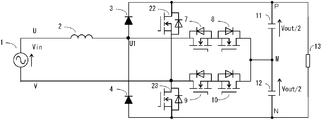
- FIG. 1 shows a first embodiment of the present invention.
- the circuit configuration is the same as that of the conventional example shown in FIG. 3, but the fast recovery diodes 5 and 6 in the conventional example are replaced with the diodes 20 and 21 for general rectification.
- This operation is as follows. Under the condition that the AC input voltage Vin is positive and the voltage relationship is Vin ⁇ Vout / 2, the gates of the MOSFETs 9 and 10 constituting the bidirectional semiconductor switch are always kept in the on signal state, and the MOSFETs 7 and 8 constituting the bidirectional semiconductor switch Perform high frequency switching. That is, the zero voltage mode and the 1 ⁇ 2 voltage mode 1a described in the conventional example are used. The diodes 20 and 21 do not conduct in both modes. Here, the 1/2 voltage mode 2a is not used.
- the gates of the MOSFETs 9 and 10 are always kept in the off signal state, and high frequency switching is performed by the MOSFETs 7 and 8. That is, the half voltage mode 2b and the full voltage mode described in the prior art are used. In both modes, the diode 21 is kept conductive and the diode 20 is kept non-conductive, so the conduction state of the diodes 20 and 21 does not change as long as operation is performed between these two modes. Is not applied. Here, the 1/2 voltage mode 1b is not used.
- the diode 21 performs reverse recovery operation only when the AC input voltage Vin falls below Vout / 2 and the MOSFETs 9 and 10 are turned on, only once in one cycle of the AC input voltage, There is no problem using a diode with a long reverse recovery time.
- the alternating current input voltage Vin is negative, and the MOSFETs 9 and 10 perform the on / off operation once in a half cycle according to the magnitude relationship of the absolute value of the alternating current input voltage Vin to Vout / 2.
- the diode 20 conducts during the off period of the MOSFET 9.
- FIG. 2 shows a second embodiment of the present invention.
- the diodes 20 and 21 in the first embodiment are replaced with MOSFETs 22 and 23, respectively.
- the MOSFET conducts in the reverse direction by applying a voltage to the gate, and the forward voltage drop can be reduced particularly when the current is small. This can be realized by providing an on signal to one of the gates of the MOSFETs 22 and 23 according to the polarity of the input current Iin when providing the off signals to the gates of the MOSFETs 9 and 10.
- the efficiency of the power conversion device not only the power conversion efficiency at the rated point, but also the energy efficiency over the entire operation period is being emphasized.
- the circuit of FIG. 2 is an effective means for improving the efficiency at light load in such a case.
- the MOSFETs 22 and 23 may be connected in parallel with the diodes 20 and 21 left.
- MOSFETs with low conduction loss actually have a long reverse recovery time of parasitic diodes if their withstand voltage is several hundred volts or more. For reasons of reason, it is unsuitable for rectification operation at high frequency, and its application is difficult.
- the present invention is characterized in that by using one side of the rectifier circuit as a low frequency operation, it is possible to perform rectification with a MOSFET of several hundreds volts withstand voltage.
- the third embodiment uses a SiC (silicon carbide) Schottky barrier diode instead of the fast recovery diode in the first and second embodiments. Since the SiC (silicon carbide) Schottky barrier diode does not have a reverse recovery operation, the switching loss can be further reduced as compared with the first and second embodiments, and the conversion efficiency of the device can be improved.
- the type of semiconductor is not limited to MOSFETs, and the configuration is a configuration in which reverse blocking switch elements are connected in antiparallel, It is also possible to realize a configuration in which switch elements are combined.
- the present invention is a proposal for a technique for reducing the loss of an AC-DC conversion circuit, and is applicable to a DC power supply, an uninterruptible power supply, a power converter for driving a motor, and the like.
Landscapes
- Engineering & Computer Science (AREA)
- Power Engineering (AREA)
- Rectifiers (AREA)
Abstract
ダイオードブリッジ回路の交流入力にリアクトルを、直流出力にコンデンサ直列回路を、コンデンサ直列接続点とダイオードブリッジ回路の各々の交流入力との間に接続された双方向スイッチとを備えた整流回路で、双方向スイッチを高周波駆動する制御では損失が大きく、発生損失が大きい。この損失低減のため、双方向スイッチの一方を交流入力電圧の周波数で、他方を高周波で駆動し、ダイオードブリッジ回路の交流入力電圧の周波数で駆動する双方向スイッチを接続したダイオードとして一般整流用ダイオードを、高周波で駆動する双方向スイッチを接続したダイオードとしてファーストリカバリダイオードを、各々用いる。
Description
本発明は、半導体スイッチング素子を用いた整流器の損失低減技術に関する。
図3に、特許文献1に記載された従来方式の回路を示す。図3において、1は交流電源、2はリアクトル、3~6はダイオード、7~10は半導体スイッチであり、ここではMOSFET(絶縁ゲート電界効果形トランジスタ)としている。MOSFETは寄生ダイオード(図示)の存在により逆方向は常に導通状態にある。MOSFETを逆直列接続することにより、順逆両方向の電流の導通、遮断を制御可能な、いわゆる双方向半導体スイッチを構成している。11、12はコンデンサ、13は負荷である。ここで、負荷としてはコンデンサ11又は12と並列接続される場合もある。
この回路は交流を直流に変換するいわゆる整流回路であり、入力電流Iinを、交流入力電圧Vinと位相の等しい正弦波波形としつつ、直流出力(PN間)電圧Voutを、交流入力電圧Vinのピーク値より高い所望の値に保つ機能を持つ。
この回路は交流を直流に変換するいわゆる整流回路であり、入力電流Iinを、交流入力電圧Vinと位相の等しい正弦波波形としつつ、直流出力(PN間)電圧Voutを、交流入力電圧Vinのピーク値より高い所望の値に保つ機能を持つ。
以下に、これらの機能を実現するための動作について説明する。
例えば、交流入力電圧Vinが正極性で、かつ電圧関係がVin<Vout/2の場合、双方向半導体スイッチ用MOSFET7~10のゲートを全てオンすると、ダイオード3と5の接続点U1の電位は直流出力のM点及び交流電源1のV点の電位と等しくなり、U1-V間電圧は0Vとなる。このため、交流電源1→リアクトル2→MOSFET7→MOSFET8→MOSFET10→MOSFET9→交流電源1の経路で電流が流れ、交流電源1の電圧Vinがリアクトル2の両端に印加され、入力電流Iinは増加する。以下、この状態を0電圧モードと称する。
例えば、交流入力電圧Vinが正極性で、かつ電圧関係がVin<Vout/2の場合、双方向半導体スイッチ用MOSFET7~10のゲートを全てオンすると、ダイオード3と5の接続点U1の電位は直流出力のM点及び交流電源1のV点の電位と等しくなり、U1-V間電圧は0Vとなる。このため、交流電源1→リアクトル2→MOSFET7→MOSFET8→MOSFET10→MOSFET9→交流電源1の経路で電流が流れ、交流電源1の電圧Vinがリアクトル2の両端に印加され、入力電流Iinは増加する。以下、この状態を0電圧モードと称する。
次に、MOSFET7をオフすると、交流電源1→リアクトル2→ダイオード3→コンデンサ11→MOSFET10→MOSFET9→交流電源1の経路で電流が流れ、コンデンサ11を充電する。この時、リアクトル2には交流入力電圧Vinとコンデンサ11の電圧Vout/2との差電圧が印加され、入力電流Iinは減少する。この時のU1-V間電圧はコンデンサ11の電圧Vout/2である。以下、この状態を1/2電圧モード1aと称する。
また、MOSFET7の代わりにMOSFET10をオフすると、交流電源1→リアクトル2→MOSFET7→MOSFET8→コンデンサ12→ダイオード6→交流電源1の経路で電流が流れ、コンデンサ12を充電する。この時、リアクトル2には交流入力電圧Vinとコンデンサ12の電圧Vout/2との差電圧が印加され、入力電流Iinは減少する。この時のU1-V間電圧はコンデンサC12の電圧Vout/2である。以下、この状態を1/2電圧モード2aと称する。
交流入力電圧Vinが正極性で、かつ電圧関係がVin>Vout/2の場合、MOSFET7と8のゲートをオフ、MOSFET9と10のゲートをオンすると、交流電源1→リアクトル2→ダイオード3→コンデンサ11→MOSFET10→MOSFET9→交流電源1の経路で電流が流れ、コンデンサ11を充電する。この時、リアクトル2には交流入力電圧Vinとコンデンサ12の電圧Vout/2との差電圧が印加され、この時は交流入力電圧Vin>コンデンサ11の電圧Vout/2であるので、入力電流Iinは増加する。この時のU1-V間電圧はコンデンサ11の電圧Vout/2である。以下、この状態を1/2電圧モード1bと称する。
同様に、MOSFET7と8のゲートをオン、MOSFET9と10のゲートをオフすると、交流電源1→リアクトル2→MOSFET7→MOSFET8→コンデンサ12→ダイオード6→交流電源1の経路で電流が流れ、コンデンサ12を充電し、入力電流Iinは増加する。この時のU1-V間電圧はコンデンサ12の電圧Vout/2である。以下、この状態を1/2電圧モード2bと称する。
即ち、上記1/2電圧モード名において、末尾の1はコンデンサ11を充電するモード、2はコンデンサ12を充電するモード、aは入力電流Iinが減少するモード、bは入力電流Iinが増加するモードであることを表す。
各々のモードから、MOSFET7~10のゲートを全てオフすると、交流電源1→リアクトル2→ダイオード3→コンデンサ11→コンデンサ12→ダイオード6→交流電源1の経路で電流が流れ、リアクトル2には交流入力電圧Vinと直流出力電圧Voutとの差電圧が印加される。装置の通常運転状態においては、交流入力電圧Vin<直流出力電圧Voutであり、入力電流Iinは減少する。この時のU1-V間電圧は直流出力電圧Voutである。以下、この状態を全電圧モードと称する。
各々のモードから、MOSFET7~10のゲートを全てオフすると、交流電源1→リアクトル2→ダイオード3→コンデンサ11→コンデンサ12→ダイオード6→交流電源1の経路で電流が流れ、リアクトル2には交流入力電圧Vinと直流出力電圧Voutとの差電圧が印加される。装置の通常運転状態においては、交流入力電圧Vin<直流出力電圧Voutであり、入力電流Iinは減少する。この時のU1-V間電圧は直流出力電圧Voutである。以下、この状態を全電圧モードと称する。
MOSFET7と8、又はMOSFET9と10を高周波でスイッチングさせ、そのオンとオフの時比率を制御することにより、上述のモードを切替えれば、入力電流Iinの波形と大きさを任意に制御できる。これにより、入力電流Iinの波形を正弦波形(ここではリプル分は無視)とし、また負荷電力に応じて入力電流Iinの振幅を制御することで直流出力電圧Voutを所望の値に保つことができる。交流入力電圧Vinが負極性の場合も同様の動作が可能である。この回路は上述のように、U1-V間電圧として、0V、Vout/2、Voutの3つの電圧を持たせることができる、いわゆる3レベル回路である。
上述の動作において、例えば入力電流Iinが正で、MOSFET7と8をオンする場合、MOSFET7のゲートをオンすれば、MOSFET8のゲートのオン、オフに関わらず、MOSFET8は寄生ダイオードにより導通状態となるが、さらにMOSFET8のゲートにオン信号を与えることにより、MOSFET8自体にも電流が流れる。ダイオードは電流に関わらず一定値以上の順電圧降下を持つが、MOSFETの順電圧降下は電流に比例する特性があるので、特に電流が小さい時に順電圧降下を低減でき、導通損失低減に効果的である。これは一般に同期整流技術として良く知られている。したがって上述のように電流極性に関わらず、導通させたいMOSFETは全てゲートにオン信号を与える制御を行う。
近年、環境問題等から電源装置にも低損失すなわち高効率であることが求められている。図3の回路において、MOSFETは各々の印加電圧がVout/2であり、直流出力電圧Voutに対する耐圧は必要ないことから、低耐圧で順電圧降下の低いものを用いることができる。さらに、上述のようにMOSFETは順電圧降下が電流に比例するので、電流容量の大きいものを用いるか、並列数を増やせばその分順電圧降下を低減できる。
一方、ダイオードの順電圧降下電圧低減には下記の課題がある。
MOSFET7と8が高周波スイッチングを行うとダイオード3と4には高周波電圧が印加され、高周波の電流の導通、遮断を行う。同様に、MOSFET 9と10が高周波スイッチングを行うとダイオード5と6に高周波電圧が印加され、高周波の電流の導通、遮断を行う。特許文献1の図2、図3等には両方の双方向半導体スイッチに高周波スイッチングをさせることが示されている。この高周波動作に耐えるために、ダイオード3~6には逆回復時間(逆電圧印加時の電流遮断時間)の短い、いわゆるファーストリカバリダイオードが用いられる。一方、ファーストリカバリダイオードは、商用周波数の整流に用いられる、いわゆる一般整流用ダイオードよりも順電圧降下が高くなる傾向にある。
MOSFET7と8が高周波スイッチングを行うとダイオード3と4には高周波電圧が印加され、高周波の電流の導通、遮断を行う。同様に、MOSFET 9と10が高周波スイッチングを行うとダイオード5と6に高周波電圧が印加され、高周波の電流の導通、遮断を行う。特許文献1の図2、図3等には両方の双方向半導体スイッチに高周波スイッチングをさせることが示されている。この高周波動作に耐えるために、ダイオード3~6には逆回復時間(逆電圧印加時の電流遮断時間)の短い、いわゆるファーストリカバリダイオードが用いられる。一方、ファーストリカバリダイオードは、商用周波数の整流に用いられる、いわゆる一般整流用ダイオードよりも順電圧降下が高くなる傾向にある。
上述の動作においてMOSFET7~10が全てオフする全電圧モードでは、入力電流Iinはダイオード2個を通過する。さらに入力電流Iinを正弦波化するにはリアクトル2の両端電圧即ち交流入力電圧Vinと、U1-V間電圧の低周波成分の差電圧が、所定の値になるよう時比率制御が行われる。このため、交流入力電圧Vinの瞬時値が高いときにはU1-V間電圧の低周波成分も高くなり、これに伴い全電圧モードの時比率も大きくなる。交流入力電圧Vinのピーク付近は力率1制御を行っているため、入力電流Iinのピーク付近であり、電流が大きい時にダイオード2個分の電圧降下を生じるため、導通損失がさらに大きくなり、装置全体の効率低下を招く。また、ファーストリカバリダイオードは整流ダイオードより高価である。特にSiC(炭化珪素)によるショットキーバリアダイオードは、逆回復損失をほとんど生じない特性があり、高周波での用途に適しているが、価格は現状では高価である。
従って、本発明の課題は、交流電圧から3レベルの直流電圧を生成する整流回路として、交流入力電流を正弦波化でき、発生損失が小さく、低価格の整流回路を提供することである。
従って、本発明の課題は、交流電圧から3レベルの直流電圧を生成する整流回路として、交流入力電流を正弦波化でき、発生損失が小さく、低価格の整流回路を提供することである。
上述の課題を解決するために、第1の発明においては、交流入力電圧を直流電圧に変換する、いわゆる整流回路であって、交流電源の一端にリアクトルの一端を接続し、前記リアクトルの他端に、ダイオード直列回路を並列接続してなるダイオードブリッジ回路の交流入力の一方を、交流電源の他端に前記ダイオードブリッジ回路の交流入力の他方を、各々接続し、前記ダイオードブリッジ回路の直流出力の端子間に複数のコンデンサを直列接続したコンデンサ直列回路を接続し、前記コンデンサ直列回路の中間接続点と、前記ダイオードブリッジ回路の交流入力の一方及び他方との間を、単一または複数の半導体素子からなり、順方向と逆方向の双方向の電流の導通、遮断を制御可能な双方向半導体スイッチを介して各々接続して構成された整流回路であり、前記ダイオード直列回路の一方を構成するダイオードは、一般整流用ダイオードに比べて逆回復時間の短い、いわゆるファーストリカバリダイオードとし、他方のダイオード直列回路を構成するダイオードは、ファーストリカバリダイオードに比べて逆回復時間が長く、かつ順電圧降下の小さい、いわゆる一般整流用ダイオードとする。
第2の発明においては、第1の発明における、前記双方向半導体スイッチの一方は前記交流入力電圧の周波数で、他方は前記交流入力電圧の周波数より高い周波数で、各々駆動する。
第3の発明においては、第1又は第2の発明における、前記一般整流用ダイオードで構成されたダイオード直列回路の直列接続点に接続された双方向半導体スイッチは前記交流入力電圧の周波数で、前記ファーストリカバリダイオードで構成されたダイオード直列回路の直列接続点に接続された双方向半導体スイッチは前記交流入力電圧の周波数より高い周波数で、各々駆動する。
第4の発明においては、第1~第3の発明における、前記一般整流用ダイオードの代わりにMOSFET(絶縁ゲート電界効果形トランジスタ)を用いる。
第5の発明においては、第1~第4の発明における、前記ファーストリカバリダイオードの代わりに、SiC(炭化珪素)によるショットキーバリアダイオードを用いる。
本発明では、交流電源の一端にリアクトルの一端を、前記リアクトルの他端にダイオードブリッジ回路の交流入力の一方を、交流電源の他端に前記ダイオードブリッジ回路の交流入力の他方を、前記ダイオードブリッジ回路の直流出力の端子間にコンデンサ直列回路を、各々接続し、前記コンデンサ直列回路の中間接続点と、前記ダイオードブリッジ回路の交流入力の一方及び他方との間を、双方向半導体スイッチを介して各々接続した整流回路において、前記ダイオード直列回路の一方を構成するダイオードは、ファーストリカバリダイオードとし、他方のダイオード直列回路を構成するダイオードは、一般整流用ダイオードとする。この時、双方向半導体スイッチの一方は交流電源の周波数で、他方は交流電源の周波数より高い高周波でオンオフさせる。
この結果、従来のファーストリカバリダイオードに代えて、一般整流用ダイオードを用いることが可能となり、損失低減と低価格化が可能となる。
この結果、従来のファーストリカバリダイオードに代えて、一般整流用ダイオードを用いることが可能となり、損失低減と低価格化が可能となる。
本発明の要点は、交流電源の一端にリアクトルの一端を、前記リアクトルの他端にダイオードブリッジ回路の交流入力の一方を、交流電源の他端に前記ダイオードブリッジ回路の交流入力の他方を、前記ダイオードブリッジ回路の直流出力の端子間にコンデンサ直列回路を、各々接続し、前記コンデンサ直列回路の中間接続点と、前記ダイオードブリッジ回路の交流入力の一方及び他方との間を、双方向半導体スイッチを介して各々接続した整流回路において、前記ダイオード直列回路の一方を構成するダイオードは、ファーストリカバリダイオードとし、他方のダイオード直列回路を構成するダイオードは、一般整流用ダイオードとして、双方向半導体スイッチの一方は交流電源の周波数で、他方は交流電源の周波数より高い高周波でオンオフさせている点である。
図1に、本発明の第1の実施例を示す。回路構成は図3に示す従来例と同等であるが、従来例におけるファーストリカバリダイオード5、6を一般整流用ダイオード20、21に置き換えている。この動作は下記の通りである。交流入力電圧Vinが正で、電圧関係がVin<Vout/2の条件では、双方向半導体スイッチを構成するMOSFET9と10のゲートを常にオン信号状態に保ち、双方向半導体スイッチを構成するMOSFET7と8で高周波スイッチングを行う。即ち、従来例で説明した0電圧モードと1/2電圧モード1aを用いる。両モードともダイオード20、21は導通しない。ここでは、1/2電圧モード2aは使用しない。
交流入力電圧Vinが正で、電圧関係がVin>Vout/2の条件では、MOSFET9と10のゲートを常にオフ信号状態に保ち、MOSFET7と8で高周波スイッチングを行う。即ち、従来例で説明した1/2電圧モード2bと全電圧モードを用いる。両モードともダイオード21が導通、ダイオード20が非導通の状態に保たれるので、この両モード間で動作している限りはダイオード20、21の導通状態は変わらず、ダイオード20、21には高周波が印加されない。ここでは、1/2電圧モード1bは使用しない。
以上の動作によれば、ダイオード21が逆回復動作となるのは交流入力電圧VinがVout/2を下回ってMOSFET9及び10がオンする時で、交流入力電圧の1サイクルに1回だけであり、逆回復時間の長いダイオードを使っても支障はない。
交流入力電圧Vinが負の場合も同様であり、MOSFET9及び10は交流入力電圧Vinの絶対値のVout/2に対する大小関係で、半サイクルに1回ずつオン、オフ動作を行う。この時はMOSFET9のオフ期間にダイオード20が導通する。
交流入力電圧Vinが負の場合も同様であり、MOSFET9及び10は交流入力電圧Vinの絶対値のVout/2に対する大小関係で、半サイクルに1回ずつオン、オフ動作を行う。この時はMOSFET9のオフ期間にダイオード20が導通する。
図2に、本発明の第2の実施例を示す。第1の実施例におけるダイオード20、21を、MOSFET22、23に置き換えたものである。上述のようにMOSFETはゲートに電圧を与えることで逆方向にも導通し、特に電流が小さい場合に順電圧降下を小さくすることができる。MOSFET9及び10のゲートにオフ信号を与える際、入力電流Iinの極性に応じてMOSFET22又は23の一方のゲートにオン信号を与えることでこれを実現できる。近年、電力変換装置の効率は、定格点での電力変換効率だけではなく、運用期間全体でのエネルギー効率が重視されつつある。例えば、情報機器用電源装置などでは定格電力ぎりぎりの負荷がかかっていることはむしろまれである。これは過負荷による電源ダウンを防止するため余裕を持たせた容量としてあるためであり、このため、50%程度の負荷や軽負荷での効率が重要になる。図2の回路はこのような場合に軽負荷時の効率改善に有効な手段となる。ダイオード20、21を残したまま並列にMOSFET22、23を接続しても良い。
尚、ダイオード3と4もMOSFETに置き換えることが一見可能なように見えるが、実際には導通損失の低いMOSFETは、数百ボルト以上の耐圧のものにおいては寄生ダイオードの逆回復時間が長いなどの理由から、高周波での整流動作に不向きであり、適用は困難である。本発明は整流回路の片側を低周波動作にすることで、数百ボルト耐圧のMOSFETによる整流を可能とした点に特徴がある。
第3の実施例は、実施例1、2におけるファーストリカバリダイオードの代わりに、SiC(炭化珪素)ショットキーバリアダイオードを用いるものである。SiC(炭化珪素)ショットキーバリアダイオードは逆回復動作がないので、スイッチング損失が実施例1や2に比べて一層低減でき、装置の変換効率を向上させることができる。
尚、上記実施例には双方向半導体スイッチとしてMOSFETを逆直列接続した構成例を示したが、半導体の種類はMOSFETに限られず、構成は逆阻止形スイッチ素子を逆並列接続した構成、ダイオードとスイッチ素子を組合せた構成などでも実現可能である。
尚、上記実施例には双方向半導体スイッチとしてMOSFETを逆直列接続した構成例を示したが、半導体の種類はMOSFETに限られず、構成は逆阻止形スイッチ素子を逆並列接続した構成、ダイオードとスイッチ素子を組合せた構成などでも実現可能である。
本発明は、交流-直流変換回路の損失低減技術の提案であり、直流電源装置、無停電電源装置、電動機駆動用電力変換装置などへの適用が可能である。
1・・・交流電源 2・・・リアクトル
3~6・・・ファーストリカバリダイオード
7~10、22、23・・・MOSFET
11、12・・・コンデンサ 13・・・負荷
20、21・・・一般整流用ダイオード
3~6・・・ファーストリカバリダイオード
7~10、22、23・・・MOSFET
11、12・・・コンデンサ 13・・・負荷
20、21・・・一般整流用ダイオード
Claims (9)
- 交流入力電圧を直流電圧に変換する、いわゆる整流回路であって、交流電源の一端にリアクトルの一端を接続し、前記リアクトルの他端に、ダイオード直列回路を並列接続してなるダイオードブリッジ回路の交流入力の一方を、交流電源の他端に前記ダイオードブリッジ回路の交流入力の他方を、各々接続し、前記ダイオードブリッジ回路の直流出力の端子間に複数のコンデンサを直列接続したコンデンサ直列回路を接続し、前記コンデンサ直列回路の中間接続点と、前記ダイオードブリッジ回路の交流入力の一方及び他方との間を、単一または複数の半導体素子からなり、順方向と逆方向の双方向の電流の導通、遮断を制御可能な双方向半導体スイッチを介して各々接続して構成された整流回路であり、前記ダイオード直列回路の一方を構成するダイオードは、一般整流用ダイオードに比べて逆回復時間の短い、いわゆるファーストリカバリダイオードとし、他方のダイオード直列回路を構成するダイオードは、ファーストリカバリダイオードに比べて逆回復時間が長く、かつ順電圧降下の小さい、いわゆる一般整流用ダイオードとすることを特徴とする整流回路。
- 前記双方向半導体スイッチの一方は前記交流入力電圧の周波数で、他方は前記交流入力電圧の周波数より高い周波数で、各々駆動することを特徴とする請求項1に記載の整流回路。
- 前記一般整流用ダイオードで構成されたダイオード直列回路の直列接続点に接続された双方向半導体スイッチは前記交流入力電圧の周波数で、前記ファーストリカバリダイオードで構成されたダイオード直列回路の直列接続点に接続された双方向半導体スイッチは前記交流入力電圧の周波数より高い周波数で、各々駆動することを特徴とする請求項1又は2に記載の整流回路。
- 前記一般整流用ダイオードの代わりにMOSFET(絶縁ゲート電界効果形トランジスタ)を用いたことを特徴とする請求項1又は2の何れかに記載の整流回路。
- 前記一般整流用ダイオードの代わりにMOSFET(絶縁ゲート電界効果形トランジスタ)を用いたことを特徴とする請求項3に記載の整流回路。
- 前記ファーストリカバリダイオードの代わりに、SiC(炭化珪素)によるショットキーバリアダイオードを用いたことを特徴とする請求項1又は2に記載の整流回路。
- 前記ファーストリカバリダイオードの代わりに、SiC(炭化珪素)によるショットキーバリアダイオードを用いたことを特徴とする請求項3に記載の整流回路。
- 前記ファーストリカバリダイオードの代わりに、SiC(炭化珪素)によるショットキーバリアダイオードを用いたことを特徴とする請求項4に記載の整流回路。
- 前記ファーストリカバリダイオードの代わりに、SiC(炭化珪素)によるショットキーバリアダイオードを用いたことを特徴とする請求項5に記載の整流回路。
Priority Applications (2)
| Application Number | Priority Date | Filing Date | Title |
|---|---|---|---|
| CN201280071145.XA CN104205602B (zh) | 2012-04-06 | 2012-10-23 | 整流电路 |
| US14/476,047 US9385624B2 (en) | 2012-04-06 | 2014-09-03 | Rectifier circuit |
Applications Claiming Priority (2)
| Application Number | Priority Date | Filing Date | Title |
|---|---|---|---|
| JP2012087718A JP6032393B2 (ja) | 2012-04-06 | 2012-04-06 | 整流回路 |
| JP2012-087718 | 2012-04-06 |
Related Child Applications (1)
| Application Number | Title | Priority Date | Filing Date |
|---|---|---|---|
| US14/476,047 Continuation US9385624B2 (en) | 2012-04-06 | 2014-09-03 | Rectifier circuit |
Publications (1)
| Publication Number | Publication Date |
|---|---|
| WO2013150573A1 true WO2013150573A1 (ja) | 2013-10-10 |
Family
ID=49300104
Family Applications (1)
| Application Number | Title | Priority Date | Filing Date |
|---|---|---|---|
| PCT/JP2012/006765 Ceased WO2013150573A1 (ja) | 2012-04-06 | 2012-10-23 | 整流回路 |
Country Status (4)
| Country | Link |
|---|---|
| US (1) | US9385624B2 (ja) |
| JP (1) | JP6032393B2 (ja) |
| CN (1) | CN104205602B (ja) |
| WO (1) | WO2013150573A1 (ja) |
Cited By (2)
| Publication number | Priority date | Publication date | Assignee | Title |
|---|---|---|---|---|
| JP2017055581A (ja) * | 2015-09-10 | 2017-03-16 | ジョンソンコントロールズ ヒタチ エア コンディショニング テクノロジー(ホンコン)リミテッド | 直流電源装置および空気調和機 |
| JP2020127363A (ja) * | 2015-09-10 | 2020-08-20 | 日立ジョンソンコントロールズ空調株式会社 | 直流電源装置および空気調和機 |
Families Citing this family (13)
| Publication number | Priority date | Publication date | Assignee | Title |
|---|---|---|---|---|
| WO2015069917A1 (en) * | 2013-11-07 | 2015-05-14 | Rompower Energy System, Inc. | Bridgeless pfc using single sided high frequency switching |
| CN104601002B (zh) * | 2014-12-29 | 2017-06-30 | 南京航空航天大学 | 一种稀疏式双级矩阵变换器拓扑结构 |
| JP6551041B2 (ja) * | 2015-08-19 | 2019-07-31 | 富士電機株式会社 | 交流−直流変換装置 |
| JP6490017B2 (ja) | 2016-01-19 | 2019-03-27 | 三菱電機株式会社 | パワーモジュール、3相インバータシステム、およびパワーモジュールの検査方法 |
| JP6955077B2 (ja) * | 2016-06-28 | 2021-10-27 | 日立ジョンソンコントロールズ空調株式会社 | 直流電源装置および空気調和機 |
| JP6798802B2 (ja) * | 2016-06-28 | 2020-12-09 | 日立ジョンソンコントロールズ空調株式会社 | 直流電源装置および空気調和機 |
| CN109643656A (zh) * | 2016-09-02 | 2019-04-16 | 新电元工业株式会社 | Mosfet以及电力转换电路 |
| FR3058593B1 (fr) * | 2016-11-10 | 2018-11-09 | Renault S.A.S | Procede de commande d'un redresseur triphase pour un dispositif de charge embarque sur un vehicule electrique ou hybride. |
| KR102455073B1 (ko) * | 2018-02-23 | 2022-10-14 | 엘지전자 주식회사 | 직류 링크 전압의 조절이 가능한 정류 장치 |
| JP7039430B2 (ja) * | 2018-09-19 | 2022-03-22 | 株式会社東芝 | Ac/dcコンバータ |
| EP3930159B1 (en) * | 2020-06-26 | 2023-05-17 | Siemens Aktiengesellschaft | Active rectifier circuit |
| CN113972830A (zh) * | 2020-07-22 | 2022-01-25 | 广东美的制冷设备有限公司 | 图腾柱功率因数校正电路、控制方法、装置及设备 |
| CN115347808B (zh) * | 2021-05-12 | 2025-10-03 | 佛山市顺德区美的电子科技有限公司 | 一种控制方法、设备、系统及存储介质 |
Citations (5)
| Publication number | Priority date | Publication date | Assignee | Title |
|---|---|---|---|---|
| JP2003009535A (ja) * | 2001-04-17 | 2003-01-10 | Matsushita Electric Ind Co Ltd | 電源装置 |
| JP2008022625A (ja) * | 2006-07-12 | 2008-01-31 | Fuji Electric Systems Co Ltd | 交流−直流変換装置 |
| JP2009095083A (ja) * | 2007-10-04 | 2009-04-30 | Fuji Electric Systems Co Ltd | 電力変換装置 |
| JP2011024285A (ja) * | 2009-07-13 | 2011-02-03 | Fuji Electric Systems Co Ltd | 電力変換装置 |
| JP2011091947A (ja) * | 2009-10-23 | 2011-05-06 | Panasonic Corp | 直流電源装置 |
Family Cites Families (12)
| Publication number | Priority date | Publication date | Assignee | Title |
|---|---|---|---|---|
| US5477131A (en) * | 1993-09-02 | 1995-12-19 | Motorola, Inc. | Zero-voltage-transition switching power converters using magnetic feedback |
| JPH08196077A (ja) * | 1994-11-18 | 1996-07-30 | Toshiba Corp | 電力変換装置及びこれを利用した空気調和装置 |
| JP3225825B2 (ja) * | 1996-01-12 | 2001-11-05 | 富士電機株式会社 | Ac/dc変換装置 |
| JP3230434B2 (ja) * | 1996-06-05 | 2001-11-19 | 富士電機株式会社 | Ac/dc変換回路 |
| US6320772B1 (en) * | 1999-05-26 | 2001-11-20 | Matsushita Electric Industrial Co., Ltd. | Converter circuit having control means with capability to short-circuit converter output |
| KR100418127B1 (ko) * | 2001-04-17 | 2004-02-11 | 마츠시타 덴끼 산교 가부시키가이샤 | 전원장치 |
| GB0321321D0 (en) * | 2003-09-11 | 2003-10-15 | Boc Group Plc | Power factor correction circuit |
| BRPI0715762A2 (pt) * | 2006-08-23 | 2013-09-24 | Neumayer Tekfor Holding Gmbh | disposiÇço de conexço entre um munhço do eixo e uma parte de articulaÇço |
| US8489136B2 (en) * | 2007-01-05 | 2013-07-16 | Aliphcom | Wireless link to transmit digital audio data between devices in a manner controlled dynamically to adapt to variable wireless error rates |
| WO2009028053A1 (ja) * | 2007-08-29 | 2009-03-05 | Mitsubishi Electric Corporation | 交流直流変換装置及びその装置を用いた圧縮機駆動装置並びに空気調和機 |
| US8823303B2 (en) | 2008-12-01 | 2014-09-02 | Mitsubishi Electric Corporation | Alternating-current direct-current converter and electric motor driver |
| CN102577067A (zh) * | 2009-10-23 | 2012-07-11 | 松下电器产业株式会社 | 直流电源装置和使用其的电动机驱动用的逆变装置 |
-
2012
- 2012-04-06 JP JP2012087718A patent/JP6032393B2/ja not_active Expired - Fee Related
- 2012-10-23 CN CN201280071145.XA patent/CN104205602B/zh not_active Expired - Fee Related
- 2012-10-23 WO PCT/JP2012/006765 patent/WO2013150573A1/ja not_active Ceased
-
2014
- 2014-09-03 US US14/476,047 patent/US9385624B2/en not_active Expired - Fee Related
Patent Citations (5)
| Publication number | Priority date | Publication date | Assignee | Title |
|---|---|---|---|---|
| JP2003009535A (ja) * | 2001-04-17 | 2003-01-10 | Matsushita Electric Ind Co Ltd | 電源装置 |
| JP2008022625A (ja) * | 2006-07-12 | 2008-01-31 | Fuji Electric Systems Co Ltd | 交流−直流変換装置 |
| JP2009095083A (ja) * | 2007-10-04 | 2009-04-30 | Fuji Electric Systems Co Ltd | 電力変換装置 |
| JP2011024285A (ja) * | 2009-07-13 | 2011-02-03 | Fuji Electric Systems Co Ltd | 電力変換装置 |
| JP2011091947A (ja) * | 2009-10-23 | 2011-05-06 | Panasonic Corp | 直流電源装置 |
Cited By (2)
| Publication number | Priority date | Publication date | Assignee | Title |
|---|---|---|---|---|
| JP2017055581A (ja) * | 2015-09-10 | 2017-03-16 | ジョンソンコントロールズ ヒタチ エア コンディショニング テクノロジー(ホンコン)リミテッド | 直流電源装置および空気調和機 |
| JP2020127363A (ja) * | 2015-09-10 | 2020-08-20 | 日立ジョンソンコントロールズ空調株式会社 | 直流電源装置および空気調和機 |
Also Published As
| Publication number | Publication date |
|---|---|
| JP6032393B2 (ja) | 2016-11-30 |
| JP2013219903A (ja) | 2013-10-24 |
| US20140369100A1 (en) | 2014-12-18 |
| CN104205602B (zh) | 2016-12-28 |
| US9385624B2 (en) | 2016-07-05 |
| CN104205602A (zh) | 2014-12-10 |
Similar Documents
| Publication | Publication Date | Title |
|---|---|---|
| JP6032393B2 (ja) | 整流回路 | |
| JP6191965B2 (ja) | 電力変換装置、およびそれを用いたパワーコンディショナ | |
| JP6454936B2 (ja) | 電力変換装置、およびそれを用いたパワーコンディショナ | |
| CN101098103B (zh) | 功率转换器开关驱动器的自供电电源 | |
| JP5049637B2 (ja) | Dc/dc電力変換装置 | |
| AU2014245740B2 (en) | Inverter device | |
| US10250159B2 (en) | Five-level inverter topology with high voltage utilization ratio | |
| JPWO2012067167A1 (ja) | 交流−交流変換装置 | |
| JP2012210104A (ja) | 電力変換装置 | |
| JP5228886B2 (ja) | スナバ回路 | |
| JP6337397B2 (ja) | 電力変換装置、およびそれを用いたパワーコンディショナ | |
| JP2015233406A (ja) | バイパス運転機能を有する直列型h−ブリッジインバータ | |
| JP6009003B2 (ja) | Dc/dcコンバータ | |
| JP6012008B2 (ja) | スイッチング回路 | |
| JP7024784B2 (ja) | 交直変換回路及び力率改善回路 | |
| JP2021180553A (ja) | Dc/dc変換装置 | |
| JP2012191761A (ja) | 交流−直流変換回路 | |
| JPWO2013136623A1 (ja) | 電力変換器及びその制御装置 | |
| JP2012239292A (ja) | 整流器のスナバ回路 | |
| WO2017064848A1 (ja) | 電力変換装置、及びそれを用いたパワーコンディショナ | |
| JP6551041B2 (ja) | 交流−直流変換装置 | |
| JP6447944B2 (ja) | 電力変換装置、及びそれを用いたパワーコンディショナ | |
| KR101681934B1 (ko) | 반전, 비반전, 매트릭스 컨버터 기능을 갖는 단상 pwm ac-ac 컨버터 및 그 구동방법 | |
| JP5980009B2 (ja) | スイッチング電源装置 | |
| JP7008494B2 (ja) | 電力変換装置 |
Legal Events
| Date | Code | Title | Description |
|---|---|---|---|
| 121 | Ep: the epo has been informed by wipo that ep was designated in this application |
Ref document number: 12873540 Country of ref document: EP Kind code of ref document: A1 |
|
| NENP | Non-entry into the national phase |
Ref country code: DE |
|
| 122 | Ep: pct application non-entry in european phase |
Ref document number: 12873540 Country of ref document: EP Kind code of ref document: A1 |