WO2013140986A1 - 有色硬質装飾部材 - Google Patents
有色硬質装飾部材 Download PDFInfo
- Publication number
- WO2013140986A1 WO2013140986A1 PCT/JP2013/055475 JP2013055475W WO2013140986A1 WO 2013140986 A1 WO2013140986 A1 WO 2013140986A1 JP 2013055475 W JP2013055475 W JP 2013055475W WO 2013140986 A1 WO2013140986 A1 WO 2013140986A1
- Authority
- WO
- WIPO (PCT)
- Prior art keywords
- layer
- metal
- colored
- film
- color
- Prior art date
- Legal status (The legal status is an assumption and is not a legal conclusion. Google has not performed a legal analysis and makes no representation as to the accuracy of the status listed.)
- Ceased
Links
Images


Classifications
-
- C—CHEMISTRY; METALLURGY
- C23—COATING METALLIC MATERIAL; COATING MATERIAL WITH METALLIC MATERIAL; CHEMICAL SURFACE TREATMENT; DIFFUSION TREATMENT OF METALLIC MATERIAL; COATING BY VACUUM EVAPORATION, BY SPUTTERING, BY ION IMPLANTATION OR BY CHEMICAL VAPOUR DEPOSITION, IN GENERAL; INHIBITING CORROSION OF METALLIC MATERIAL OR INCRUSTATION IN GENERAL
- C23C—COATING METALLIC MATERIAL; COATING MATERIAL WITH METALLIC MATERIAL; SURFACE TREATMENT OF METALLIC MATERIAL BY DIFFUSION INTO THE SURFACE, BY CHEMICAL CONVERSION OR SUBSTITUTION; COATING BY VACUUM EVAPORATION, BY SPUTTERING, BY ION IMPLANTATION OR BY CHEMICAL VAPOUR DEPOSITION, IN GENERAL
- C23C30/00—Coating with metallic material characterised only by the composition of the metallic material, i.e. not characterised by the coating process
-
- B—PERFORMING OPERATIONS; TRANSPORTING
- B32—LAYERED PRODUCTS
- B32B—LAYERED PRODUCTS, i.e. PRODUCTS BUILT-UP OF STRATA OF FLAT OR NON-FLAT, e.g. CELLULAR OR HONEYCOMB, FORM
- B32B37/00—Methods or apparatus for laminating, e.g. by curing or by ultrasonic bonding
- B32B37/02—Methods or apparatus for laminating, e.g. by curing or by ultrasonic bonding characterised by a sequence of laminating steps, e.g. by adding new layers at consecutive laminating stations
-
- B—PERFORMING OPERATIONS; TRANSPORTING
- B32—LAYERED PRODUCTS
- B32B—LAYERED PRODUCTS, i.e. PRODUCTS BUILT-UP OF STRATA OF FLAT OR NON-FLAT, e.g. CELLULAR OR HONEYCOMB, FORM
- B32B37/00—Methods or apparatus for laminating, e.g. by curing or by ultrasonic bonding
- B32B37/14—Methods or apparatus for laminating, e.g. by curing or by ultrasonic bonding characterised by the properties of the layers
- B32B37/24—Methods or apparatus for laminating, e.g. by curing or by ultrasonic bonding characterised by the properties of the layers with at least one layer not being coherent before laminating, e.g. made up from granular material sprinkled onto a substrate
-
- B—PERFORMING OPERATIONS; TRANSPORTING
- B32—LAYERED PRODUCTS
- B32B—LAYERED PRODUCTS, i.e. PRODUCTS BUILT-UP OF STRATA OF FLAT OR NON-FLAT, e.g. CELLULAR OR HONEYCOMB, FORM
- B32B38/00—Ancillary operations in connection with laminating processes
- B32B38/10—Removing layers, or parts of layers, mechanically or chemically
-
- B—PERFORMING OPERATIONS; TRANSPORTING
- B32—LAYERED PRODUCTS
- B32B—LAYERED PRODUCTS, i.e. PRODUCTS BUILT-UP OF STRATA OF FLAT OR NON-FLAT, e.g. CELLULAR OR HONEYCOMB, FORM
- B32B9/00—Layered products comprising a layer of a particular substance not covered by groups B32B11/00 - B32B29/00
- B32B9/04—Layered products comprising a layer of a particular substance not covered by groups B32B11/00 - B32B29/00 comprising such particular substance as the main or only constituent of a layer, which is next to another layer of the same or of a different material
-
- C—CHEMISTRY; METALLURGY
- C23—COATING METALLIC MATERIAL; COATING MATERIAL WITH METALLIC MATERIAL; CHEMICAL SURFACE TREATMENT; DIFFUSION TREATMENT OF METALLIC MATERIAL; COATING BY VACUUM EVAPORATION, BY SPUTTERING, BY ION IMPLANTATION OR BY CHEMICAL VAPOUR DEPOSITION, IN GENERAL; INHIBITING CORROSION OF METALLIC MATERIAL OR INCRUSTATION IN GENERAL
- C23C—COATING METALLIC MATERIAL; COATING MATERIAL WITH METALLIC MATERIAL; SURFACE TREATMENT OF METALLIC MATERIAL BY DIFFUSION INTO THE SURFACE, BY CHEMICAL CONVERSION OR SUBSTITUTION; COATING BY VACUUM EVAPORATION, BY SPUTTERING, BY ION IMPLANTATION OR BY CHEMICAL VAPOUR DEPOSITION, IN GENERAL
- C23C14/00—Coating by vacuum evaporation, by sputtering or by ion implantation of the coating forming material
- C23C14/0015—Coating by vacuum evaporation, by sputtering or by ion implantation of the coating forming material characterized by the colour of the layer
-
- C—CHEMISTRY; METALLURGY
- C23—COATING METALLIC MATERIAL; COATING MATERIAL WITH METALLIC MATERIAL; CHEMICAL SURFACE TREATMENT; DIFFUSION TREATMENT OF METALLIC MATERIAL; COATING BY VACUUM EVAPORATION, BY SPUTTERING, BY ION IMPLANTATION OR BY CHEMICAL VAPOUR DEPOSITION, IN GENERAL; INHIBITING CORROSION OF METALLIC MATERIAL OR INCRUSTATION IN GENERAL
- C23C—COATING METALLIC MATERIAL; COATING MATERIAL WITH METALLIC MATERIAL; SURFACE TREATMENT OF METALLIC MATERIAL BY DIFFUSION INTO THE SURFACE, BY CHEMICAL CONVERSION OR SUBSTITUTION; COATING BY VACUUM EVAPORATION, BY SPUTTERING, BY ION IMPLANTATION OR BY CHEMICAL VAPOUR DEPOSITION, IN GENERAL
- C23C14/00—Coating by vacuum evaporation, by sputtering or by ion implantation of the coating forming material
- C23C14/0021—Reactive sputtering or evaporation
- C23C14/0036—Reactive sputtering
- C23C14/0084—Producing gradient compositions
-
- C—CHEMISTRY; METALLURGY
- C23—COATING METALLIC MATERIAL; COATING MATERIAL WITH METALLIC MATERIAL; CHEMICAL SURFACE TREATMENT; DIFFUSION TREATMENT OF METALLIC MATERIAL; COATING BY VACUUM EVAPORATION, BY SPUTTERING, BY ION IMPLANTATION OR BY CHEMICAL VAPOUR DEPOSITION, IN GENERAL; INHIBITING CORROSION OF METALLIC MATERIAL OR INCRUSTATION IN GENERAL
- C23C—COATING METALLIC MATERIAL; COATING MATERIAL WITH METALLIC MATERIAL; SURFACE TREATMENT OF METALLIC MATERIAL BY DIFFUSION INTO THE SURFACE, BY CHEMICAL CONVERSION OR SUBSTITUTION; COATING BY VACUUM EVAPORATION, BY SPUTTERING, BY ION IMPLANTATION OR BY CHEMICAL VAPOUR DEPOSITION, IN GENERAL
- C23C14/00—Coating by vacuum evaporation, by sputtering or by ion implantation of the coating forming material
- C23C14/02—Pretreatment of the material to be coated
- C23C14/024—Deposition of sublayers, e.g. to promote adhesion of the coating
- C23C14/025—Metallic sublayers
-
- C—CHEMISTRY; METALLURGY
- C23—COATING METALLIC MATERIAL; COATING MATERIAL WITH METALLIC MATERIAL; CHEMICAL SURFACE TREATMENT; DIFFUSION TREATMENT OF METALLIC MATERIAL; COATING BY VACUUM EVAPORATION, BY SPUTTERING, BY ION IMPLANTATION OR BY CHEMICAL VAPOUR DEPOSITION, IN GENERAL; INHIBITING CORROSION OF METALLIC MATERIAL OR INCRUSTATION IN GENERAL
- C23C—COATING METALLIC MATERIAL; COATING MATERIAL WITH METALLIC MATERIAL; SURFACE TREATMENT OF METALLIC MATERIAL BY DIFFUSION INTO THE SURFACE, BY CHEMICAL CONVERSION OR SUBSTITUTION; COATING BY VACUUM EVAPORATION, BY SPUTTERING, BY ION IMPLANTATION OR BY CHEMICAL VAPOUR DEPOSITION, IN GENERAL
- C23C14/00—Coating by vacuum evaporation, by sputtering or by ion implantation of the coating forming material
- C23C14/02—Pretreatment of the material to be coated
- C23C14/027—Graded interfaces
-
- C—CHEMISTRY; METALLURGY
- C23—COATING METALLIC MATERIAL; COATING MATERIAL WITH METALLIC MATERIAL; CHEMICAL SURFACE TREATMENT; DIFFUSION TREATMENT OF METALLIC MATERIAL; COATING BY VACUUM EVAPORATION, BY SPUTTERING, BY ION IMPLANTATION OR BY CHEMICAL VAPOUR DEPOSITION, IN GENERAL; INHIBITING CORROSION OF METALLIC MATERIAL OR INCRUSTATION IN GENERAL
- C23C—COATING METALLIC MATERIAL; COATING MATERIAL WITH METALLIC MATERIAL; SURFACE TREATMENT OF METALLIC MATERIAL BY DIFFUSION INTO THE SURFACE, BY CHEMICAL CONVERSION OR SUBSTITUTION; COATING BY VACUUM EVAPORATION, BY SPUTTERING, BY ION IMPLANTATION OR BY CHEMICAL VAPOUR DEPOSITION, IN GENERAL
- C23C14/00—Coating by vacuum evaporation, by sputtering or by ion implantation of the coating forming material
- C23C14/06—Coating by vacuum evaporation, by sputtering or by ion implantation of the coating forming material characterised by the coating material
- C23C14/08—Oxides
- C23C14/083—Oxides of refractory metals or yttrium
-
- C—CHEMISTRY; METALLURGY
- C23—COATING METALLIC MATERIAL; COATING MATERIAL WITH METALLIC MATERIAL; CHEMICAL SURFACE TREATMENT; DIFFUSION TREATMENT OF METALLIC MATERIAL; COATING BY VACUUM EVAPORATION, BY SPUTTERING, BY ION IMPLANTATION OR BY CHEMICAL VAPOUR DEPOSITION, IN GENERAL; INHIBITING CORROSION OF METALLIC MATERIAL OR INCRUSTATION IN GENERAL
- C23C—COATING METALLIC MATERIAL; COATING MATERIAL WITH METALLIC MATERIAL; SURFACE TREATMENT OF METALLIC MATERIAL BY DIFFUSION INTO THE SURFACE, BY CHEMICAL CONVERSION OR SUBSTITUTION; COATING BY VACUUM EVAPORATION, BY SPUTTERING, BY ION IMPLANTATION OR BY CHEMICAL VAPOUR DEPOSITION, IN GENERAL
- C23C14/00—Coating by vacuum evaporation, by sputtering or by ion implantation of the coating forming material
- C23C14/06—Coating by vacuum evaporation, by sputtering or by ion implantation of the coating forming material characterised by the coating material
- C23C14/14—Metallic material, boron or silicon
- C23C14/20—Metallic material, boron or silicon on organic substrates
-
- C—CHEMISTRY; METALLURGY
- C23—COATING METALLIC MATERIAL; COATING MATERIAL WITH METALLIC MATERIAL; CHEMICAL SURFACE TREATMENT; DIFFUSION TREATMENT OF METALLIC MATERIAL; COATING BY VACUUM EVAPORATION, BY SPUTTERING, BY ION IMPLANTATION OR BY CHEMICAL VAPOUR DEPOSITION, IN GENERAL; INHIBITING CORROSION OF METALLIC MATERIAL OR INCRUSTATION IN GENERAL
- C23C—COATING METALLIC MATERIAL; COATING MATERIAL WITH METALLIC MATERIAL; SURFACE TREATMENT OF METALLIC MATERIAL BY DIFFUSION INTO THE SURFACE, BY CHEMICAL CONVERSION OR SUBSTITUTION; COATING BY VACUUM EVAPORATION, BY SPUTTERING, BY ION IMPLANTATION OR BY CHEMICAL VAPOUR DEPOSITION, IN GENERAL
- C23C14/00—Coating by vacuum evaporation, by sputtering or by ion implantation of the coating forming material
- C23C14/22—Coating by vacuum evaporation, by sputtering or by ion implantation of the coating forming material characterised by the process of coating
- C23C14/34—Sputtering
-
- C—CHEMISTRY; METALLURGY
- C23—COATING METALLIC MATERIAL; COATING MATERIAL WITH METALLIC MATERIAL; CHEMICAL SURFACE TREATMENT; DIFFUSION TREATMENT OF METALLIC MATERIAL; COATING BY VACUUM EVAPORATION, BY SPUTTERING, BY ION IMPLANTATION OR BY CHEMICAL VAPOUR DEPOSITION, IN GENERAL; INHIBITING CORROSION OF METALLIC MATERIAL OR INCRUSTATION IN GENERAL
- C23C—COATING METALLIC MATERIAL; COATING MATERIAL WITH METALLIC MATERIAL; SURFACE TREATMENT OF METALLIC MATERIAL BY DIFFUSION INTO THE SURFACE, BY CHEMICAL CONVERSION OR SUBSTITUTION; COATING BY VACUUM EVAPORATION, BY SPUTTERING, BY ION IMPLANTATION OR BY CHEMICAL VAPOUR DEPOSITION, IN GENERAL
- C23C28/00—Coating for obtaining at least two superposed coatings either by methods not provided for in a single one of groups C23C2/00 - C23C26/00 or by combinations of methods provided for in subclasses C23C and C25C or C25D
- C23C28/04—Coating for obtaining at least two superposed coatings either by methods not provided for in a single one of groups C23C2/00 - C23C26/00 or by combinations of methods provided for in subclasses C23C and C25C or C25D only coatings of inorganic non-metallic material
- C23C28/042—Coating for obtaining at least two superposed coatings either by methods not provided for in a single one of groups C23C2/00 - C23C26/00 or by combinations of methods provided for in subclasses C23C and C25C or C25D only coatings of inorganic non-metallic material including a refractory ceramic layer, e.g. refractory metal oxides, ZrO2, rare earth oxides
-
- C—CHEMISTRY; METALLURGY
- C23—COATING METALLIC MATERIAL; COATING MATERIAL WITH METALLIC MATERIAL; CHEMICAL SURFACE TREATMENT; DIFFUSION TREATMENT OF METALLIC MATERIAL; COATING BY VACUUM EVAPORATION, BY SPUTTERING, BY ION IMPLANTATION OR BY CHEMICAL VAPOUR DEPOSITION, IN GENERAL; INHIBITING CORROSION OF METALLIC MATERIAL OR INCRUSTATION IN GENERAL
- C23C—COATING METALLIC MATERIAL; COATING MATERIAL WITH METALLIC MATERIAL; SURFACE TREATMENT OF METALLIC MATERIAL BY DIFFUSION INTO THE SURFACE, BY CHEMICAL CONVERSION OR SUBSTITUTION; COATING BY VACUUM EVAPORATION, BY SPUTTERING, BY ION IMPLANTATION OR BY CHEMICAL VAPOUR DEPOSITION, IN GENERAL
- C23C28/00—Coating for obtaining at least two superposed coatings either by methods not provided for in a single one of groups C23C2/00 - C23C26/00 or by combinations of methods provided for in subclasses C23C and C25C or C25D
- C23C28/04—Coating for obtaining at least two superposed coatings either by methods not provided for in a single one of groups C23C2/00 - C23C26/00 or by combinations of methods provided for in subclasses C23C and C25C or C25D only coatings of inorganic non-metallic material
- C23C28/048—Coating for obtaining at least two superposed coatings either by methods not provided for in a single one of groups C23C2/00 - C23C26/00 or by combinations of methods provided for in subclasses C23C and C25C or C25D only coatings of inorganic non-metallic material with layers graded in composition or physical properties
-
- C—CHEMISTRY; METALLURGY
- C23—COATING METALLIC MATERIAL; COATING MATERIAL WITH METALLIC MATERIAL; CHEMICAL SURFACE TREATMENT; DIFFUSION TREATMENT OF METALLIC MATERIAL; COATING BY VACUUM EVAPORATION, BY SPUTTERING, BY ION IMPLANTATION OR BY CHEMICAL VAPOUR DEPOSITION, IN GENERAL; INHIBITING CORROSION OF METALLIC MATERIAL OR INCRUSTATION IN GENERAL
- C23C—COATING METALLIC MATERIAL; COATING MATERIAL WITH METALLIC MATERIAL; SURFACE TREATMENT OF METALLIC MATERIAL BY DIFFUSION INTO THE SURFACE, BY CHEMICAL CONVERSION OR SUBSTITUTION; COATING BY VACUUM EVAPORATION, BY SPUTTERING, BY ION IMPLANTATION OR BY CHEMICAL VAPOUR DEPOSITION, IN GENERAL
- C23C28/00—Coating for obtaining at least two superposed coatings either by methods not provided for in a single one of groups C23C2/00 - C23C26/00 or by combinations of methods provided for in subclasses C23C and C25C or C25D
- C23C28/30—Coatings combining at least one metallic layer and at least one inorganic non-metallic layer
- C23C28/32—Coatings combining at least one metallic layer and at least one inorganic non-metallic layer including at least one pure metallic layer
- C23C28/322—Coatings combining at least one metallic layer and at least one inorganic non-metallic layer including at least one pure metallic layer only coatings of metal elements only
-
- C—CHEMISTRY; METALLURGY
- C23—COATING METALLIC MATERIAL; COATING MATERIAL WITH METALLIC MATERIAL; CHEMICAL SURFACE TREATMENT; DIFFUSION TREATMENT OF METALLIC MATERIAL; COATING BY VACUUM EVAPORATION, BY SPUTTERING, BY ION IMPLANTATION OR BY CHEMICAL VAPOUR DEPOSITION, IN GENERAL; INHIBITING CORROSION OF METALLIC MATERIAL OR INCRUSTATION IN GENERAL
- C23C—COATING METALLIC MATERIAL; COATING MATERIAL WITH METALLIC MATERIAL; SURFACE TREATMENT OF METALLIC MATERIAL BY DIFFUSION INTO THE SURFACE, BY CHEMICAL CONVERSION OR SUBSTITUTION; COATING BY VACUUM EVAPORATION, BY SPUTTERING, BY ION IMPLANTATION OR BY CHEMICAL VAPOUR DEPOSITION, IN GENERAL
- C23C28/00—Coating for obtaining at least two superposed coatings either by methods not provided for in a single one of groups C23C2/00 - C23C26/00 or by combinations of methods provided for in subclasses C23C and C25C or C25D
- C23C28/30—Coatings combining at least one metallic layer and at least one inorganic non-metallic layer
- C23C28/34—Coatings combining at least one metallic layer and at least one inorganic non-metallic layer including at least one inorganic non-metallic material layer, e.g. metal carbide, nitride, boride, silicide layer and their mixtures, enamels, phosphates and sulphates
- C23C28/341—Coatings combining at least one metallic layer and at least one inorganic non-metallic layer including at least one inorganic non-metallic material layer, e.g. metal carbide, nitride, boride, silicide layer and their mixtures, enamels, phosphates and sulphates with at least one carbide layer
-
- C—CHEMISTRY; METALLURGY
- C23—COATING METALLIC MATERIAL; COATING MATERIAL WITH METALLIC MATERIAL; CHEMICAL SURFACE TREATMENT; DIFFUSION TREATMENT OF METALLIC MATERIAL; COATING BY VACUUM EVAPORATION, BY SPUTTERING, BY ION IMPLANTATION OR BY CHEMICAL VAPOUR DEPOSITION, IN GENERAL; INHIBITING CORROSION OF METALLIC MATERIAL OR INCRUSTATION IN GENERAL
- C23C—COATING METALLIC MATERIAL; COATING MATERIAL WITH METALLIC MATERIAL; SURFACE TREATMENT OF METALLIC MATERIAL BY DIFFUSION INTO THE SURFACE, BY CHEMICAL CONVERSION OR SUBSTITUTION; COATING BY VACUUM EVAPORATION, BY SPUTTERING, BY ION IMPLANTATION OR BY CHEMICAL VAPOUR DEPOSITION, IN GENERAL
- C23C28/00—Coating for obtaining at least two superposed coatings either by methods not provided for in a single one of groups C23C2/00 - C23C26/00 or by combinations of methods provided for in subclasses C23C and C25C or C25D
- C23C28/30—Coatings combining at least one metallic layer and at least one inorganic non-metallic layer
- C23C28/34—Coatings combining at least one metallic layer and at least one inorganic non-metallic layer including at least one inorganic non-metallic material layer, e.g. metal carbide, nitride, boride, silicide layer and their mixtures, enamels, phosphates and sulphates
- C23C28/343—Coatings combining at least one metallic layer and at least one inorganic non-metallic layer including at least one inorganic non-metallic material layer, e.g. metal carbide, nitride, boride, silicide layer and their mixtures, enamels, phosphates and sulphates with at least one DLC or an amorphous carbon based layer, the layer being doped or not
-
- C—CHEMISTRY; METALLURGY
- C23—COATING METALLIC MATERIAL; COATING MATERIAL WITH METALLIC MATERIAL; CHEMICAL SURFACE TREATMENT; DIFFUSION TREATMENT OF METALLIC MATERIAL; COATING BY VACUUM EVAPORATION, BY SPUTTERING, BY ION IMPLANTATION OR BY CHEMICAL VAPOUR DEPOSITION, IN GENERAL; INHIBITING CORROSION OF METALLIC MATERIAL OR INCRUSTATION IN GENERAL
- C23C—COATING METALLIC MATERIAL; COATING MATERIAL WITH METALLIC MATERIAL; SURFACE TREATMENT OF METALLIC MATERIAL BY DIFFUSION INTO THE SURFACE, BY CHEMICAL CONVERSION OR SUBSTITUTION; COATING BY VACUUM EVAPORATION, BY SPUTTERING, BY ION IMPLANTATION OR BY CHEMICAL VAPOUR DEPOSITION, IN GENERAL
- C23C28/00—Coating for obtaining at least two superposed coatings either by methods not provided for in a single one of groups C23C2/00 - C23C26/00 or by combinations of methods provided for in subclasses C23C and C25C or C25D
- C23C28/30—Coatings combining at least one metallic layer and at least one inorganic non-metallic layer
- C23C28/34—Coatings combining at least one metallic layer and at least one inorganic non-metallic layer including at least one inorganic non-metallic material layer, e.g. metal carbide, nitride, boride, silicide layer and their mixtures, enamels, phosphates and sulphates
- C23C28/345—Coatings combining at least one metallic layer and at least one inorganic non-metallic layer including at least one inorganic non-metallic material layer, e.g. metal carbide, nitride, boride, silicide layer and their mixtures, enamels, phosphates and sulphates with at least one oxide layer
-
- C—CHEMISTRY; METALLURGY
- C23—COATING METALLIC MATERIAL; COATING MATERIAL WITH METALLIC MATERIAL; CHEMICAL SURFACE TREATMENT; DIFFUSION TREATMENT OF METALLIC MATERIAL; COATING BY VACUUM EVAPORATION, BY SPUTTERING, BY ION IMPLANTATION OR BY CHEMICAL VAPOUR DEPOSITION, IN GENERAL; INHIBITING CORROSION OF METALLIC MATERIAL OR INCRUSTATION IN GENERAL
- C23C—COATING METALLIC MATERIAL; COATING MATERIAL WITH METALLIC MATERIAL; SURFACE TREATMENT OF METALLIC MATERIAL BY DIFFUSION INTO THE SURFACE, BY CHEMICAL CONVERSION OR SUBSTITUTION; COATING BY VACUUM EVAPORATION, BY SPUTTERING, BY ION IMPLANTATION OR BY CHEMICAL VAPOUR DEPOSITION, IN GENERAL
- C23C28/00—Coating for obtaining at least two superposed coatings either by methods not provided for in a single one of groups C23C2/00 - C23C26/00 or by combinations of methods provided for in subclasses C23C and C25C or C25D
- C23C28/30—Coatings combining at least one metallic layer and at least one inorganic non-metallic layer
- C23C28/36—Coatings combining at least one metallic layer and at least one inorganic non-metallic layer including layers graded in composition or physical properties
-
- B—PERFORMING OPERATIONS; TRANSPORTING
- B32—LAYERED PRODUCTS
- B32B—LAYERED PRODUCTS, i.e. PRODUCTS BUILT-UP OF STRATA OF FLAT OR NON-FLAT, e.g. CELLULAR OR HONEYCOMB, FORM
- B32B37/00—Methods or apparatus for laminating, e.g. by curing or by ultrasonic bonding
- B32B37/14—Methods or apparatus for laminating, e.g. by curing or by ultrasonic bonding characterised by the properties of the layers
- B32B37/24—Methods or apparatus for laminating, e.g. by curing or by ultrasonic bonding characterised by the properties of the layers with at least one layer not being coherent before laminating, e.g. made up from granular material sprinkled onto a substrate
- B32B2037/246—Vapour deposition
-
- B—PERFORMING OPERATIONS; TRANSPORTING
- B32—LAYERED PRODUCTS
- B32B—LAYERED PRODUCTS, i.e. PRODUCTS BUILT-UP OF STRATA OF FLAT OR NON-FLAT, e.g. CELLULAR OR HONEYCOMB, FORM
- B32B2310/00—Treatment by energy or chemical effects
- B32B2310/021—Treatment by energy or chemical effects using electrical effects
-
- B—PERFORMING OPERATIONS; TRANSPORTING
- B32—LAYERED PRODUCTS
- B32B—LAYERED PRODUCTS, i.e. PRODUCTS BUILT-UP OF STRATA OF FLAT OR NON-FLAT, e.g. CELLULAR OR HONEYCOMB, FORM
- B32B2310/00—Treatment by energy or chemical effects
- B32B2310/04—Treatment by energy or chemical effects using liquids, gas or steam
- B32B2310/0409—Treatment by energy or chemical effects using liquids, gas or steam using liquids
-
- B—PERFORMING OPERATIONS; TRANSPORTING
- B32—LAYERED PRODUCTS
- B32B—LAYERED PRODUCTS, i.e. PRODUCTS BUILT-UP OF STRATA OF FLAT OR NON-FLAT, e.g. CELLULAR OR HONEYCOMB, FORM
- B32B2311/00—Metals, their alloys or their compounds
-
- Y—GENERAL TAGGING OF NEW TECHNOLOGICAL DEVELOPMENTS; GENERAL TAGGING OF CROSS-SECTIONAL TECHNOLOGIES SPANNING OVER SEVERAL SECTIONS OF THE IPC; TECHNICAL SUBJECTS COVERED BY FORMER USPC CROSS-REFERENCE ART COLLECTIONS [XRACs] AND DIGESTS
- Y10—TECHNICAL SUBJECTS COVERED BY FORMER USPC
- Y10T—TECHNICAL SUBJECTS COVERED BY FORMER US CLASSIFICATION
- Y10T428/00—Stock material or miscellaneous articles
- Y10T428/30—Self-sustaining carbon mass or layer with impregnant or other layer
Definitions
- the present invention relates to colored hard decorative members such as exterior parts of watches, accessories such as eyeglasses and accessories, and ornaments, and is particularly rich in various color variations with a high-class feeling, and has scratch resistance and wear resistance over a long period of time.
- the present invention relates to a colored hard decorative member having excellent properties and corrosion resistance.
- the outermost layer has a lightness for a high-class appearance.
- a high platinum film was formed.
- a base layer is formed on a substrate, a titanium carbide layer is formed on this surface by a dry plating method, and a decorative coating layer made of platinum or a platinum alloy formed on this surface by a dry plating method Is forming.
- the platinum layer as the outermost layer is expensive, it is necessary to form a thin film, and it is necessary to make the titanium carbide layer light in order to suppress a color change when the thin platinum layer peels off. For this reason, the hardness of the titanium carbide layer is lower than that of the original titanium carbide layer (about 40%), and sufficient scratch resistance could not be obtained.
- the scratch resistance in order to improve the scratch resistance, if the amount of carbon reacted with the titanium carbide layer is increased to increase the hardness, the scratch resistance increases but the color tone becomes dark.
- the thickness of the titanium carbide layer which is a hardened layer, is increased in order to improve scratch resistance, film peeling due to increased film stress and pitting corrosion is likely to occur in the corrosion resistance test. It was difficult to form a film thickness of 1.0 ⁇ m or more.
- a hard carbon film (DLC film) described in Patent Document 3 a dielectric film described in Patent Document 4, or Patent Document 5
- a method for forming a multi-colored film having the two-tone color described has also been proposed, but the base substrate lacks wear resistance and adhesion, has low scratch resistance as a decorative member, is easily damaged, and has good appearance. There was a problem of lowering.
- An object of the present invention is to provide a colored hard decorative member that suppresses deterioration in appearance quality due to scratches and wear by significantly improving scratch resistance and has various color variations with a high-class feeling.
- the colored hard decorative member of the present invention adopts the configuration described below.
- the colored hard decorative member of the present invention includes an adhesion layer made of a lower oxide of an alloy having a high adhesion effect on a base material, an alloy compound gradient adhesion layer in which the reaction gas content is gradually increased, and an alloy compound wear-resistant layer. And an alloy compound color-raising gradient layer in which the reaction gas content is decreased in a gradient, and a colored decorative layer.
- a film made of an alloy of (Cr, Ti, Hf, Zr) that improves the corrosion resistance as necessary the alloy adhesion layer having a high adhesion effect on the substrate and the reaction gas content increased in a gradient manner. It consists of an alloy gradient adhesion layer, a hard wear-resistant layer, and an alloy color-graded gradient layer whose reaction gas content is gradually reduced, so that the adhesion between the substrate and the film is significantly improved and scratch resistance is achieved.
- the wear resistance layer with high film hardness can be formed thickly, the scratch resistance can be further improved, and the noble metal film having a white color, the hard film exhibiting a gold color, black DLC hard film having dielectric and dielectric film having interference effect Colored decorative layer is laminated all or part selected et.
- the gist of the present invention is as follows. (1) Base material, metal M1 and metal M2 laminated on the base material, and an adhesive layer composed of a lower oxide layer of an alloy obtained by selectively combining metal M3, metal M4 and metal laminated on the adhesive layer M5, a gradient adhesion layer composed of a reaction compound of an alloy obtained by selectively combining metal M6 and a nonmetallic element selected from one or more of nitrogen, carbon, and oxygen, and a metal laminated on the gradient adhesion layer On the wear-resistant layer and the wear-resistant layer comprising a reaction compound of an alloy composed of M7 and metal M8, and optionally a metal M9 and a non-metallic element selected from one or more of nitrogen, carbon and oxygen A color-increased inclined layer comprising a reaction compound of a metal M10 and a metal M11 laminated together, and an alloy obtained by selectively combining the metal M12 and a nonmetallic element selected from one or more of nitrogen, carbon, and oxygen, And color raising A colored hard decorative member composed of
- the content of the nonmetallic element in the reaction compound constituting the adhesion layer increases in the thickness direction as it is separated from the substrate, and the content of the nonmetallic element in the reaction compound that constitutes the color-raising gradient layer is separated from the substrate.
- the colored decorative layer is a white noble metal film of Pt, Pd, or Rh, and an intermetallic compound of the metal in the color rising gradient layer and the white noble metal is formed at the boundary with the color raising gradient layer.
- the colored hard decorative member according to (1), wherein the colored decorative layer is a DLC (diamond-like carbon) hard film.
- the colored hard decorative member according to (1), wherein the colored decorative layer is a dielectric layer formed by forming a dielectric film as a single layer or a multilayer.
- Non-metals in the reaction mixture constituting the gradient adhesion layer comprising a gradient adhesion layer composed of a reaction compound with a non-metallic element selected from one or more of nitrogen, carbon, and oxygen of an alloy that is a combination of metal M6
- a step of forming a wear-resistant layer comprising a reaction compound with a non-metallic element selected from one or more of oxygen, and a nitrogen of an alloy in which metal M10 and metal M11, and further metal M12 are combined on the wear-resistant layer
- the metals M2, M5, M8 and M11 are selected from one or two of Nb and Ta, respectively, and the metals M3, M6, M9 and M12 are one or two of Cr, Ti and Hf, respectively.
- the manufacturing method of the colored hard decoration member chosen from seed
- the gradient adhesion layer in the reactive sputtering method, is formed by increasing or decreasing the amount of the reaction gas containing the nonmetallic element in time series, and the color-gradation gradient layer is formed.
- a method for manufacturing a decorative member (11) The above (8) to (8) further comprising the steps of applying a mask to a part of the colored decorative layer and peeling the unmasked portion of the colored decorative layer with an acid or alkali to make the colored decorative layer a two-tone structure. The method for producing a colored hard decorative member according to any one of (10).
- the present invention it is possible to provide a colored hard decorative member that suppresses deterioration in appearance quality due to scratches or wear and has various color variations with a high-class feeling.
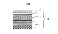
- the cross-sectional schematic diagram which shows an example of the structure of the colored hard decoration member of this invention is shown.
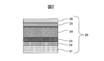
- the cross-sectional schematic diagram of the colored hard decorative member of Example 1 is shown.
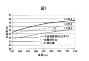
- the reflective characteristic of the colored hard decorative member of Example 1 and a comparative material is shown.
- the change of the hardness at the time of changing the methane gas amount of the colored hard decoration member of Example 1 is shown.
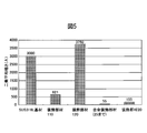
- the colored hard decorative member of Example 1 and the scratch resistance of a comparative material are shown.
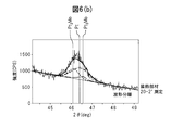
- the figure which measured the crystallinity of the colored hard decoration member of Example 1 is shown.
- the figure which measured the crystallinity of the colored hard decoration member of Example 1 is shown.
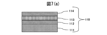
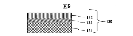
- the cross-sectional schematic diagram of the decoration member of the prior art example (formed by patent document 1) of Example 1 is shown.
- the cross-sectional schematic diagram of the decorative member of the comparative material of Example 1 is shown.
- the cross-sectional schematic diagram of the colored hard decoration member of Example 2 is shown.
- the cross-sectional schematic diagram of the decoration member which is a comparative material of Example 2 is shown.
- the colored hard decorative member of Example 2 and the scratch resistance of a comparative material are shown.
- the cross-sectional schematic diagram of the colored hard decorative member of Example 3 is shown.
- the colored hard decorative member of Example 3 and the scratch resistance of a comparative material are shown.
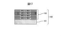
- the cross-sectional schematic diagram of the comparative material of Example 4 is shown.
- the cross-sectional schematic diagram of the colored hard decoration member of Example 4 is shown.
- the reflection characteristic with the incident angle of the colored hard decoration member of Example 4 is shown.
- the colored hard decorative member of Example 4 and the scratch resistance of a comparative material are shown.
- the cross-sectional schematic diagram of the comparative material of Example 5 is shown.
- the cross-sectional schematic diagram of the colored hard decoration member of Example 5 is shown.
- the reflective characteristic with the colored hard decoration member incident angle of Example 5 is shown.
- the colored hard decorative member of Example 6 and the scratch resistance of a comparative material are shown.
- the cross-sectional schematic diagram of the colored hard decoration member of Example 6 is shown.
- FIG. 1 is a schematic sectional view showing an example of the structure of the colored hard decorative member of the present invention.
- the adhesion layer 12 made of a lower oxide of MoNb alloy is formed on the surface of the SUS316L substrate 11 as the substrate, and the gradient adhesion in which the nitrogen content is gradually increased to the lower oxide of the MoNb alloy on the adhesion layer 12 MoNb alloy color-raised gradient layer in which the layer 13 is formed, the wear resistant layer 14 of the MoNb alloy nitride layer is formed on the gradient adhesion layer 13, and the nitrogen content is gradually decreased on the wear resistant layer 14 15 is formed, and the colored decorative layer 16 is formed on the MoNb alloy color-raising inclined layer 15.
- the colored hard decorative member of the present invention since the decorative film exhibiting various colors is formed on the alloy film having high scratch resistance, the colored hard decorative member having various color variations having high scratch resistance is obtained. It has the feature that it can.
- the colored hard decorative member of the present invention there is no clear interface between the adhesion layer 12 and the inclined adhesion layer 13, high adhesion to the base material is ensured, and the film stress increases in a gradient manner, resulting in stress distortion. As a result, crack resistance and abrasion resistance can be suppressed, and scratch resistance and wear resistance can be improved. Further, since the wear-resistant layer 14 having high film hardness can be formed thicker, higher scratch resistance can be obtained.
- the wear-resistant layer 14 of the colored hard decorative member 10 is composed of a MoNb alloy nitride layer formed with a nitrogen content showing the maximum hardness, the composite hardness of the entire hard decorative member can be increased. High scratch resistance can be obtained.
- the color-graded inclined layer 15 of the colored hard decorative member 10 has a structure in which the nonmetallic element content is gradually decreased from the wear-resistant layer 14, the color tone is gradually increased from the wear-resistant layer and the metallic luster is increased. There can be a high quality color.
- the appearance color of the colored hard decorative member 10 can be obtained in various color variations by the colored decorative layer 16. Further, since the colored decorative layer 16 is formed on the alloy member having high scratch resistance (11 to 15), it is possible to obtain a colored hard decorative member that is hard to be scratched and has a high-class feeling.
- the base material 11 is preferably a base material formed from metal or ceramics.
- the metal including alloy
- the metal include stainless steel, titanium, titanium alloy, copper, copper alloy, tungsten or hardened stainless steel, titanium, titanium alloy, and the like. These metals can be used alone or in combination of two or more. Further, the shape of the substrate 11 is not limited.
- the adhesion layer 12 is an alloy of a metal (M1) selected from one or two of Mo and W and a metal (M2) selected from one or two of Nb and Ta, or Cr, Ti, Hf. , A lower oxide film of an alloy to which a metal (M3) selected from one or more of Zr is added, and is selected depending on the compatibility with the base material and the use environment of the film.
- the adhesion layer 12 is made of a lower oxide film of these alloys, but may contain a small amount of carbon or nitrogen.
- the alloy contains metals such as V, B, Al, Si, Mn, Co, La, Ce, Y, and Sc within a total amount of 5 wt% in the alloy. May be.
- the oxygen content in the alloy metal lower oxide film of the adhesion layer is desirably 5 to 60 atm%, particularly preferably 5 to 45 atm%, based on the metal.
- the oxygen content is less than 5 atm%, there is no difference in the adhesion from the alloy metal film, and when it is 60 atm%, the adhesion is lowered and the scratch resistance is also lowered.
- the thickness of the adhesion layer of the alloy lower oxide film is preferably 0.03 to 0.3 ⁇ m. In order to obtain the effect of improving the adhesion by the adhesion layer, there is an effective effect at 0.03 ⁇ m or more, and even if it is thicker than 0.3 ⁇ m, there is not much change in the adhesion effect.
- the inclined adhesion layer 13 is an alloy of a metal M4 selected from one or two of Mo and W and a metal M5 selected from one or two of Nb and Ta, or Cr, Ti, Hf, and Zr. It is a reaction compound of an alloy added with metal M6 selected from one or more types and a nonmetallic element selected from one or more types of carbon, nitrogen and oxygen, and the content of nonmetallic elements is graded. It is composed of an increased film.
- the inclined adhesion layer 13 is preferably a film in which the content of one or more nonmetallic elements of carbon, nitrogen, and oxygen is increased in a gradient manner, such as a carbide film, a nitride film, a carbonitride film, and an oxynitride. It consists of a material film, an oxycarbide film, an oxynitride carbide film, and the like. The material to be selected is determined by the compatibility with the adhesion layer 12 and the wear-resistant layer 14 and the use environment of the coating.
- the alloy includes metals such as V, B, Al, Si, Mn, Co, La, Ce, Y, and Sc within a total amount of 5 wt% in the alloy. It may be.
- the gradient adhesion layer is a gradient in which the content of carbon, nitrogen, oxygen, or one or more selected non-metallic elements in the gradient adhesion layer is gradually increased from 0 to 50 atm% with respect to the alloy metal element. It is a membrane.
- the gradient adhesion layer preferably contains 5 to 25 atm% of oxygen, and further has a structure in which the content of carbon, nitrogen, or a mixed element thereof is gradually increased in the range of 0 to 50 atm%. Is desirable.
- the thickness of the inclined adhesion layer is desirably 0.05 to 0.3 ⁇ m. In order to obtain the effect of the inclined adhesion layer, it is necessary to be 0.05 ⁇ m or more, and even if it is thicker than 0.3 ⁇ m, the adhesion effect is not so great.
- the wear-resistant layer 14 is made of an alloy of a metal M7 selected from one or two of Mo and W and a metal M8 selected from one or two of Nb and Ta, or Cr, Ti, Hf, and Zr. It forms from the reaction compound of the alloy which added the metal (M9) chosen from 1 type, or 2 or more types, and the nonmetallic element chosen from 1 type, or 2 or more types of carbon, nitrogen, and oxygen.
- the material to be selected is determined by the desired appearance color and the usage environment of the coating.
- the alloy includes metals such as V, B, Al, Si, Mn, Co, La, Ce, Y, and Sc within a total amount of 5 wt% in the alloy. It may be.
- the content of carbon, nitrogen or mixed elements in the wear resistant layer is 5 to 70 atm%.
- the thickness of the wear-resistant layer is desirably 0.3 to 4 ⁇ m, and the film hardness is desirably HV2000 or more. Since the scratch resistance performance is approximately dependent on the film thickness and film hardness of the wear-resistant layer, it is desirable that the film thickness and film hardness be as high as possible.
- the color-raising gradient layer 15 is made of an alloy of a metal M10 selected from one or two of Mo and W and a metal M11 selected from one or two of Nb and Ta, or Cr, Ti, Hf, and Zr. It is a reaction compound of an alloy added with a metal M12 selected from one or more kinds and a nonmetallic element selected from one or more kinds of carbon, nitrogen and oxygen, and the content of the nonmetallic elements is graded. Reduce to form.
- the color raising gradient layer 15 is made of a carbide film, a nitride film, a carbonitride film, an oxynitride film, an oxycarbide film, an oxynitride carbide film, or the like.
- the material to be selected is determined by the compatibility with the wear-resistant layer 14, the desired appearance color, and the usage environment of the coating.
- the alloy includes metals such as V, B, Al, Si, Mn, Co, La, Ce, Y, and Sc within a total amount of 5 wt% in the alloy. It may be.
- the color-graded gradient layer is a gradient film in which the content of non-metallic elements, preferably carbon, nitrogen, or a mixed element thereof in the color-graded gradient layer is gradually decreased to 50-0 atm% with respect to the alloy metal element. ing.
- the thickness of the color raising gradient layer is preferably 0.05 to 0.3 ⁇ m.
- the thickness of the color-raising gradient layer is 0.05 ⁇ m or less, the color of the wear-resistant layer cannot be sufficiently raised. Further, when the thickness is 0.3 ⁇ m or more, the color of the wear-resistant layer can be sufficiently increased, but the scratch resistance is deteriorated because the thickness of the color-increased inclined layer having low hardness is increased.
- the colored decorative layer 16 includes a white noble metal film such as Pt, Pd, and Rh having higher brightness, a metal nitride film such as TiN, ZrN, and HfN that exhibits gold, and TiCN, ZrCN, HfCN, and TiON that exhibit pink to brown colors. , ZrON, HfON and other metal carbonitride films, metal oxynitride films, DLC (diamond-like carbon) films exhibiting black color, or dielectric films composed of a single layer or multiple layers of dielectric films that can produce various colors by interference effects It is produced by forming the layer on all or part of the color-raising gradient layer (two-tone structure).
- a white noble metal film such as Pt, Pd, and Rh having higher brightness
- a metal nitride film such as TiN, ZrN, and HfN that exhibits gold
- TiCN, ZrCN, HfCN, and TiON that exhibit pink to brown colors.
- the film thickness of the white noble metal constituting the colored decorative layer is preferably 0.02 to 0.2 ⁇ m.
- the thickness is 0.02 ⁇ m or less, the brightness of the color-raising gradient layer cannot be sufficiently increased.
- the thickness is 0.2 ⁇ m or more, the brightness of the color-inclined inclined layer can be sufficiently increased, but the scratch resistance is deteriorated because the thickness of the noble metal layer having low hardness is increased.
- the hard film composed of nitrogen, nitrogen and carbon, and nitrogen and oxygen of Ti, Zr, and Hf constituting the colored decorative layer exhibits a golden, pink, or brown color depending on the composition.
- the film thickness is desirably 0.05 ⁇ m or more, and if it is 0.05 ⁇ m or less, the color tone of the color-graded inclined layer exhibiting white cannot be sufficiently covered. Also, when the wear occurs, the white color of the ground becomes visible.
- the DLC (diamond-like carbon) film constituting the colored decorative layer exhibits a black color.
- the film thickness is desirably 0.05 ⁇ m or more. If it is 0.05 ⁇ m or less, the color tone of the color-graded inclined layer that exhibits white cannot be sufficiently covered. Also, when the wear occurs, the white color of the ground becomes visible.
- a single-layer or multilayer adhesion layer made of Si or Ti between the DLC film and the color-gradient gradient layer.
- the dielectric layer constituting the colored decorative layer can create various colors by the interference effect, and can be designed and controlled by a widely known dielectric multilayer interference design technique.
- a widely known dielectric multilayer interference design technique By forming a single-layer or multiple-layer dielectric film, it is possible to obtain decorative members that exhibit transparency, high saturation, and various color tones.
- the reflection color and saturation of the dielectric multilayer film can be freely adjusted by design.
- the design obtained by the dielectric multilayer interference design technology can be manufactured with good reproducibility regardless of the color tone of the hard coating, and the color tone depending on the incident angle. Can be suppressed.
- the total thickness of the dielectric layer is desirably 0.05 ⁇ m or more. If it is 0.05 ⁇ m or less, the color tone of the color-graded inclined layer that exhibits white cannot be sufficiently covered. Also, when the wear occurs, the white color of the ground becomes visible.
- a single-layer or multilayer adhesion layer made of Si or Ti between the dielectric layer and the color-graded gradient layer.
- the dielectric layer is formed on the outermost surface, it is desirable to form a dielectric film having the highest possible hardness on the outermost layer.
- the outermost layer include Si nitride, nitrocarbide, oxynitride, Al oxide, nitride, oxynitride, and the like.
- Each laminate constituting the colored hard decorative member of the present invention can be formed by a sputtering method, a CVD method, an ion plating method or the like, but is preferably formed by a reactive sputtering method.
- the colored hard decorative member 10 according to the embodiment of the present invention is manufactured by a reactive sputtering method.
- an inert gas mainly Ar gas
- a DC or AC high voltage is applied between the substrate and the target composed of the constituent atoms of the coating to ionize the substrate.
- Ar is collided with a target to form a repelled target material on a substrate.
- a trace amount of reactive gas together with the inert gas, a compound film of target constituent atoms and reactive gas can be formed on the substrate.
- the decorative member 10 of the embodiment can be manufactured by controlling the adhesion, film hardness, and color tone by adjusting the selection and amount of target constituent atoms and reactive gases.
- the reactive sputtering method has high controllability of film quality and film thickness and is easy to automate. Further, since the energy of the sputtered atoms is high, it is not necessary to heat the substrate for improving the adhesion, and a film can be formed even on a substrate such as a plastic having a low melting point. In addition, since the target material that has been blown off is formed on the substrate, it is possible to form a film even with a high melting point material, and the material can be freely selected.
- a carbide film, a nitride film, a carbonitride film, an oxynitride film, an oxycarbide film, an oxynitride carbide film, and the like can be easily formed by selecting and mixing reactive gases. Also, by alloying the target constituent atoms, it is possible to form alloy films, alloy carbide films, nitride films, carbonitride films, oxynitride films, oxycarbide films, oxynitride carbide films, etc. Become.
- the inclined adhesion layer 13 and the color raising inclined layer 15 of the colored hard decorative member 10 according to the embodiment of the present invention are formed by increasing or decreasing the amount of the reactive gas selected in time series.
- the amount of reactive gas is controlled by an automatically controlled mass flow controller, and the color tone and hardness of the layer can be controlled by the amount of reactive gas.
- the outermost colored decorative layer can have a two-tone structure having a so-called two-tone color.
- the two-tone structure can be formed by a known method.
- a method for obtaining a two-tone structure includes a step of applying a mask to a part of a colored decorative layer, a step of peeling a colored decorative layer that is not masked with an acid such as hot nitric acid, a step of peeling the mask, and an acid peeling.
- the reduction treatment is, for example, a step of removing the surface oxide film with a thiourea-based treatment agent.
- the stripping of the colored decorative film is not limited to acids, and stripping solutions suitable for the respective materials can be used, and are selected in relation to the corrosion resistance of the hard member serving as the base.
- the colored decorative layer has a two-tone structure
- a hard golden film formed of TiN, ZrN, or the like can be made into a multicolor film, and a high-quality feeling with more decorativeness can be obtained.
- the two-tone structure can be applied not only to a hard film but also to any other colored decorative layer such as a white base metal film, a DLC hard film, and a dielectric film.
- the present invention can provide a colored hard decorative member having a high-grade color tone, it can be used for a decorative part such as an exterior part of a watch, an accessory such as glasses or an accessory, a decorative article, or a sports equipment.
- a decorative part such as an exterior part of a watch, an accessory such as glasses or an accessory, a decorative article, or a sports equipment.
- the colored hard decorative member described above can be applied to some of its constituent parts, for example, exterior parts.
- the timepiece may be any of a photovoltaic power generation timepiece, a thermoelectric generation timepiece, a standard time radio wave reception type self-correcting timepiece, a mechanical timepiece, and a general electronic timepiece. Such a timepiece is manufactured by a known method using the colored hard decorative member.
- a watch is an example of a decorative member that is easily damaged by rubbing with a shirt or colliding with a desk or wall.
- the colored hard decorative member of the present invention can be formed on a timepiece, it is possible to maintain a state where the appearance is very beautiful and the appearance is very difficult to be scratched.
- the hard decorative member described above can be used for a bezel, a lug, a case, a crown, a push button, a band, and the like of a watch.
- the scratch resistance test is carried out as follows. A decorative film is applied to a SUS316L base material defined in JIS, and a worn paper in which alumina particles are uniformly dispersed is brought into contact with a test sample at a constant load, and scratches are generated by rubbing a predetermined number of times. The surface of the test sample with scratches was scanned in the direction perpendicular to the scratch direction, the surface roughness was measured, and the scratch resistance was evaluated as the mean square roughness. The greater the amount of scratches, the deeper the depth of the scratches, the larger the mean square roughness value. Conversely, the smaller the amount of scratches, the smaller the scratch depth, the smaller the mean square roughness value. Therefore, the scratch resistance can be numerically evaluated by this scratch resistance test method.
- the film hardness was measured using a micro indentation hardness tester (H100 manufactured by FISCHER). A Vickers indenter was used as a measuring element. The Vickers indenter was inserted into the sample with a 5 mN load, held for 10 seconds, then unloaded, and the film hardness was calculated from the depth of the indent formed by the insertion of the Vickers indenter.
- H100 micro indentation hardness tester
- ⁇ Color tone measurement method The color tone (brightness and saturation) of the decorative member was measured using Apectra Magic NX manufactured by KNICA MINOLTA. Using the light source D65, the L * a * b * of each film according to the L * a * b * chromaticity diagram was measured, and the brightness L * was measured.
- Example 1 As the sputtering target of Example 1, a sintered body of Mo 45 wt% Nb 55 wt% and a metal Pt target were used. As shown in FIG. 2, a SUS316L material defined in JIS was used as the base material 21, and an adhesion layer 22 made of a lower oxide of a MoNb alloy was formed on the base material 21 by a sputtering method. Next, the gradient adhesion layer 23 of the MoNb alloy oxycarbide film was formed to have a thickness of 0.2 ⁇ m by gradually increasing the methane gas while introducing a small amount of oxygen gas. Thereafter, a 2.2 ⁇ m thin wear-resistant layer 24 made of a MoNb alloy carbide film was formed.
- the color-increasing inclined layer 25 of the MoNb alloy carbide film was formed to have a thickness of 0.1 ⁇ m. Thereafter, methane gas was stopped and only argon gas was flowed to form a Pt film having a thickness of 0.05 ⁇ m, thereby producing a colored hard decorative member 20.
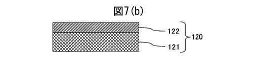
- FIG. 3 shows the colored hard decorative member 20 obtained in Example 1 and a hard decorative member (hereinafter referred to as a hard decorative member) composed of laminates 21 to 25 without forming the Pt layer 26 in the same configuration as the colored hard decorative member.
- FIG. 5 is a comparative diagram comparing the reflection characteristics with an alloy decoration member.
- the appearance color of the colored hard decorative member 20 in the Lab color space display is L *: 85.8, a *: 0.81, b *: 3.48, and the colored hard decorative member 20 forms a Pt layer.
- the brightness was much higher than that of the non-alloyed decorative member, and the appearance color of the SUS316L base material 21 was higher than L *: 85.1, a *: 0.38, b *: 2.34. .
- FIG. 4 is a diagram showing changes in hardness and brightness when the amount of introduced methane gas is changed in the colored hard decorative member 20 of Example 1 with a constant Ar gas amount of 105 sccm.
- the change in film hardness had a peak, and the brightness gradually decreased as the amount of methane gas introduced increased.
- an oxygen gas of 5 sccm was introduced under the condition of the methane gas introduction amount of 0 sccm in FIG. 3 to form a MoNb lower oxide film having a thickness of 0.1 ⁇ m.
- the adhesion to the substrate becomes higher than that of the MoNb alloy film, thereby improving the scratch resistance.
- the amount of methane gas introduced in FIG. 3 was increased from 0 sccm to 35 sccm showing the maximum hardness, thereby forming a 0.2 ⁇ m MoNb alloy carbide film.
- a 2.2 ⁇ m MoNb alloy carbide film was formed under the condition of a methane gas introduction amount of 35 sccm indicating the maximum hardness.
- the color-increasing gradient layer 25 the methane gas introduction amount was decreased gradually from the methane gas introduction amount 35 sccm showing the maximum hardness in FIG. 3 to 0 sccm, thereby forming a MoNb alloy carbide film having a thickness of 0.2 ⁇ m.
- FIG. 5 is a diagram showing the results of measuring the scratch resistance performance of the colored hard decorative member 20 of Example 1.
- the scratch resistance (root mean square roughness) of the decorative member 120 formed on the base material and the SUS316L base material on which the hard film was not formed was measured. From FIG. 5, even if compared with the decorative member 110 produced based on the SUS316L base material which does not form the hard film, and the patent document 1 shown in FIG. It was confirmed to have much better scratch resistance.
- FIGS. 6A and 6B are diagrams showing the results of measuring the crystallinity of the colored hard decorative member 20 shown in FIG. 2 by X-ray diffraction. From the crystallinity measurement, it was found that Pt 3 Mo which is an intermetallic compound of Pt and Mo was formed between the Pt film and the alloy film. Due to the presence of this intermetallic compound, the adhesion between the alloy film and the Pt film is strengthened, and it is presumed that peeling does not occur at all even if a scratch resistance test is performed. Therefore, the scratch resistance of the colored hard decorative member 20 is estimated to be higher than that of the decorative member 120 in which only the soft Pt film is formed on the SUS316L base material shown in FIG.
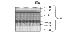
- Example 2 As the sputtering target of Example 2, a sintered body of Mo 30 wt% Ta 70 wt% and a metal Ti target were used. As shown in FIG. 8, a SUS316L material defined in JIS was used as the base material 31, and an adhesion layer 32 made of a lower oxide of a MoTa alloy was formed on the base material 31 by a sputtering method. Thereafter, the methane gas was increased in a gradient while introducing a small amount of oxygen gas to form a 0.2 ⁇ m gradient adhesion layer 33 of the MoTa alloy oxycarbide film. Thereafter, a thin wear-resistant layer 34 made of a MoTa alloy carbide film was formed to 2.0 ⁇ m.
- the methane gas was decreased in an inclined manner to form a colored layer 35 of a MoTa alloy carbide film having a thickness of 0.1 ⁇ m.
- the sputtering of the MoTa alloy was stopped, the Ti target was discharged while introducing argon gas and nitrogen gas, and the TiN film 36 was formed to have a thickness of 0.2 ⁇ m, whereby the colored hard decorative member 30 was produced.
- the color appearance of the colored hard decorative member 30 obtained in Example 2 according to the Lab color space display is L *: 77.85, a *: 3.92, b *: 37.18. Exhibited a golden color.
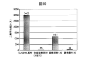
- FIG. 10 is a diagram showing the results of measuring the scratch resistance performance of the colored hard decorative member 30 of Example 2.
- the colored hard decorative member 30 of Example 2 according to the present invention as a comparative material, a SUS316L material defined in JIS shown in FIG. 9 has a Ti film 132 of 0.1 ⁇ m, and a TiN film 133 of 0.2 ⁇ m thereon. Measurement of scratch resistance (root mean square roughness) of the decorative member 130 formed and formed, the SUS316L base material on which the hard film is not formed, and the alloy decorative member (up to 35) on which the TiN film 36 is not formed in the decorative member 30 did. From FIG.
- the colored hard decorative member 30 of Example 2 of the present invention has much better scratch resistance than the SUS316L base material and the decorative member 130 on which no hard film is formed. . Further, it can be seen that the scratch resistance performance of the colored hard decorative member 30 of Example 2 of the present invention is hardly inferior to that of the alloy decorative member (up to 35).
- Scratch resistance is roughly determined by the product of the hardness of the wear-resistant layer, the thickness of the wear-resistant layer, the degree of adhesion to the base material, and the hardness of the base material.
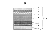
- Example 3 As the sputtering target of Example 3, a sintered body of Mo 60 wt% Nb 30 wt% Cr 10 wt%, a metal Ti, and a metal Si target were used. As shown in FIG. 11, SUS316L material prescribed
- a thin wear-resistant layer 44 made of a MoNbCr alloy carbide film was formed to 2.2 ⁇ m. Thereafter, the methane gas was decreased in an inclined manner to form a colored layer 45 of a MoNbCr alloy carbide film having a thickness of 0.1 ⁇ m. Thereafter, sputtering of the MoNbCr alloy is stopped, the Ti target is discharged while introducing argon gas, and a Ti film 46 is formed to have a thickness of 0.05 ⁇ m. Thereafter, sputtering of the Ti target is stopped, and while introducing argon gas, the Si film 47 was formed to a thickness of 0.1 ⁇ m.
- a DLC film 48 was formed to a thickness of 0.7 ⁇ m by a plasma CVD method in which methane gas was introduced to produce a colored hard decorative member 40.
- the color appearance of the colored hard decorative member 40 obtained in Example 3 according to the Lab color space display is L *: 48.75, a *: 0.26, b *: 1.8. Exhibited a black color.
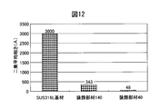
- FIG. 12 shows the result of measuring the scratch resistance performance of the colored hard decorative member 40 of Example 3.
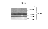
- the colored hard decorative member 40 of Example 3 according to the present invention as a comparative material, a SUS316L material defined in JIS shown in FIG. 13, a Ti film 142 (thickness: 0.05 ⁇ m), a Si film 143 (thickness: Scratch resistance (root mean square roughness) was measured for the decorative member 140 on which 0.1 ⁇ m) and the DLC film 144 (thickness: 0.7 ⁇ m) and the SUS316L base material on which the hard film was not formed. From FIG. 12, it was confirmed that the colored hard decorative member 40 of Example 3 of the present invention has much better scratch resistance as compared to the SUS316L base material and the decorative member 140 on which no hard film is formed.
- the scratch resistance is roughly determined by the product of the hardness of the abrasion resistant layer, the film thickness of the abrasion resistant layer, the adhesion to the base material, and the hardness of the base material. Therefore, the DLC film is formed on the alloy film having high scratch resistance. Is formed with good adhesion, it is possible to form a black hard member having high scratch resistance.
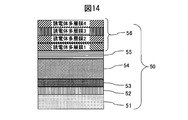
- Example 4 As the sputtering target of Example 4, a sintered body of Mo 45 wt% Nb 55 wt% and a metal Si target were used. As shown in FIG. 14, SUS316L material prescribed
- a thin wear-resistant layer 54 made of a MoNb alloy carbide film was formed to 2.2 ⁇ m. Thereafter, the methane gas was decreased in an inclined manner, thereby forming a colored raising inclined layer 55 of the MoNb alloy carbide film with a thickness of 0.1 ⁇ m. Thereafter, sputtering of the MoNb alloy was stopped, the Si target was discharged while introducing argon gas, and the film thickness was controlled to form a 0.072 ⁇ m Si film.
- a Si 3 N 4 film (thickness: 0.07 ⁇ m), a SiO 2 film (thickness: 0.061 ⁇ m), a Si 3 N 4 film (thickness: 0.03 ⁇ m) with a controlled film thickness are formed on the Si film. ) Is laminated to form a colored hard decorative member 50.
- the color appearance of the colored hard decorative member 50 obtained in Example 4 according to the Lab color space display is L *: 64.18, a *: 38.03, b *: 5.19. Had a bright red color.
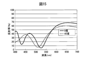
- FIG. 15 is a diagram showing the reflection characteristics according to the incident angle of the decorative member 50 of Example 4. It can be seen that the reflectance of the decorative member 50 is high as a whole, and that the difference in reflectance due to the difference in incident angle is small. Therefore, the decorative member 50 of Example 4 has a higher saturation and brighter colors than the case where the dielectric multilayer film 56 is laminated to form a single layer. In addition, in a single layer, a change in color tone occurs depending on the incident angle, but by stacking the dielectric multilayer film 56, it is possible to suppress a change in color tone due to the incident angle. Furthermore, by forming an Si film having a high absorption coefficient as an adhesion layer on the dielectric multilayer film 56, the change in color tone due to the incident angle can be extremely reduced.
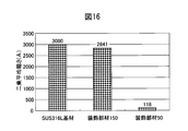
- FIG. 16 is a diagram showing the results of measuring the scratch resistance performance of the colored hard decorative member 50 of Example 4.
- the colored hard decorative member 50 of Example 4 according to the present invention as a comparative material, a decorative member 150 in which only a dielectric film is formed in a multilayer on the SUS316L material defined in JIS shown in FIG. 17, and a hard film are formed.
- the scratch resistance root mean square roughness
- Scratch resistance is roughly determined by the product of the hardness of the wear-resistant layer, the thickness of the wear-resistant layer, the adhesion to the substrate, and the hardness of the substrate.
- the dielectric film 56 exhibiting interference need not be a Si film. However, in the case of using a Si-based film, it is effective to improve the scratch resistance by forming a high hardness Si 3 N 4 film on the outermost surface.
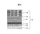
- Example 5 As the sputtering target of Example 5, a sintered body of Mo 45 wt% Nb 55 wt% and a metal Si target were used. As shown in FIG. 18, SUS316L material prescribed
- a 2.2 ⁇ m thin wear-resistant layer 64 made of a MoNb alloy nitride film was formed. Thereafter, the nitrogen gas was decreased in an inclined manner, thereby forming the colored gradient layer 65 of the MoNb alloy nitride film to be 0.1 ⁇ m. Thereafter, sputtering of the MoNb alloy was stopped, the Si target was discharged while introducing argon gas, and the film thickness was controlled to form a Si film of 0.03 ⁇ m.
- a colored hard decorative member 60 was produced by laminating and forming a dielectric multilayer film 66 composed of three layers.
- the color appearance of the colored hard decorative member 60 obtained in Example 5 according to the Lab color space display is L *: 63.11, a *: -12.61, b *: -44.5.
- the member 60 exhibited a bright blue color.
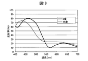
- FIG. 19 is a diagram showing the reflection characteristics according to the incident angle of the decorative member 60 of Example 5.
- FIG. 19 shows that the reflectance is high at a wavelength of 400 to 500 nm, and that the difference in reflectance due to the difference in incident angle is small. Since the decorative member 60 of Example 5 is formed by laminating the dielectric multilayer film 66, it has higher saturation and is brighter than the case where it is formed as a single layer. In addition, in a single layer, a change in color tone occurs depending on the incident angle, but by stacking the dielectric laminated film 66, a change in color tone due to the incident angle can be suppressed. Furthermore, by inserting a Si film having a high absorption coefficient into the dielectric laminated film 66, the change in color tone due to the incident angle can be extremely reduced.
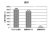
- FIG. 20 is a diagram showing the results of measuring the scratch resistance performance of the colored hard decorative member 60 of Example 5.
- a colored hard decorative member 60 of Example 5 according to the present invention a decorative member 150 in which only a dielectric multilayer film showing blue is formed on a SUS316L material defined in JIS shown in FIG.
- the scratch resistance (root mean square roughness) of the SUS316L base material not formed was measured. From FIG. 20, it was confirmed that the colored hard decorative member 60 of Example 5 of the present invention has much better scratch resistance than the SUS316L base material and the decorative member 150 that do not form a hard film. .
- Scratch resistance is roughly determined by the product of the hardness of the wear-resistant layer, the thickness of the wear-resistant layer, the adhesion to the substrate, and the hardness of the substrate.
- the dielectric film 66 exhibiting interference need not be a Si-based film. However, in the case of using a Si-based film, it is more effective for scratch resistance performance to form a Si 3 N 4 film having high hardness on the outermost surface.
- Example 6 Using the SUS316L material defined in JIS as the base material 71, the same coating compositions 71 to 76 as shown in FIGS. 18 to 66 of Example 5 were formed on the base material 71. Next, masking (not shown) was performed on part of the dielectric laminated film 76. Thereafter, the unmasked portion was peeled off using hot phosphoric acid and an alkaline solvent, and then the masking was removed, thereby producing a two-tone colored hard decorative member 70 shown in FIG. As shown in FIG.
- the surface of the colored hard decorative member 70 has a structure in which a color-inclined inclined layer 75 and a dielectric film interference layer 76 are mixed, resulting in a white and blue two-tone color and a high decorative property.
- a hard member can be obtained.
- a metal having a high adhesion effect with a metal and a high brightness and a metal having a high film hardness and a high corrosion resistance are used, and the adhesion effect on the substrate is high. Because it consists of an alloy adhesion layer, an alloy gradient adhesion layer whose reaction gas content increases in a gradient, a hard wear-resistant layer, and an alloy color-graded gradient layer whose reaction gas content decreases in a gradient.
- the adhesion between the substrate and the film is remarkably improved and the scratch resistance is improved, and the wear layer having high film hardness can be formed thickly, so that the scratch resistance can be further improved and the outermost layer has a high-class feeling.
- the present invention can provide a colored hard decorative member that suppresses deterioration in appearance quality due to scratches, wear, and the like and has a high-quality color tone and rich in color variations. It can be used for accessories such as accessories, decorative items, and various decorative members such as sports equipment.
Landscapes
- Chemical & Material Sciences (AREA)
- Engineering & Computer Science (AREA)
- Mechanical Engineering (AREA)
- Chemical Kinetics & Catalysis (AREA)
- Materials Engineering (AREA)
- Metallurgy (AREA)
- Organic Chemistry (AREA)
- Inorganic Chemistry (AREA)
- Ceramic Engineering (AREA)
- Physical Vapour Deposition (AREA)
- Chemical Vapour Deposition (AREA)
- Adornments (AREA)
Priority Applications (3)
| Application Number | Priority Date | Filing Date | Title |
|---|---|---|---|
| US14/385,165 US9464355B2 (en) | 2012-03-19 | 2013-02-28 | Colored rigid decorative member |
| EP13765000.8A EP2829631B1 (en) | 2012-03-19 | 2013-02-28 | Colored rigid decorative member |
| CN201380015069.5A CN104220634B (zh) | 2012-03-19 | 2013-02-28 | 有色硬质装饰构件 |
Applications Claiming Priority (2)
| Application Number | Priority Date | Filing Date | Title |
|---|---|---|---|
| JP2012062471A JP5930783B2 (ja) | 2012-03-19 | 2012-03-19 | 有色硬質装飾部材 |
| JP2012-062471 | 2012-03-19 |
Publications (1)
| Publication Number | Publication Date |
|---|---|
| WO2013140986A1 true WO2013140986A1 (ja) | 2013-09-26 |
Family
ID=49222449
Family Applications (1)
| Application Number | Title | Priority Date | Filing Date |
|---|---|---|---|
| PCT/JP2013/055475 Ceased WO2013140986A1 (ja) | 2012-03-19 | 2013-02-28 | 有色硬質装飾部材 |
Country Status (5)
| Country | Link |
|---|---|
| US (1) | US9464355B2 (enExample) |
| EP (1) | EP2829631B1 (enExample) |
| JP (1) | JP5930783B2 (enExample) |
| CN (1) | CN104220634B (enExample) |
| WO (1) | WO2013140986A1 (enExample) |
Cited By (1)
| Publication number | Priority date | Publication date | Assignee | Title |
|---|---|---|---|---|
| US20140315014A1 (en) * | 2013-03-08 | 2014-10-23 | Vapor Technologies, Inc. | Coated Article Having A Vivid Color |
Families Citing this family (7)
| Publication number | Priority date | Publication date | Assignee | Title |
|---|---|---|---|---|
| US8974896B2 (en) * | 2013-03-08 | 2015-03-10 | Vapor Technologies, Inc. | Coated article with dark color |
| JP6084286B2 (ja) * | 2013-03-29 | 2017-02-22 | シチズン時計株式会社 | グレー色調層を有する硬質装飾部材 |
| CN107338416A (zh) * | 2017-07-03 | 2017-11-10 | 济宁学院 | ZrMoCN梯度复合涂层刀具及其制备方法 |
| KR102594844B1 (ko) | 2018-04-10 | 2023-10-27 | 주식회사 엘지화학 | 장식 부재 |
| CN108517488B (zh) * | 2018-05-14 | 2019-07-09 | 武汉大学 | 一种合金材料部件表面防腐耐磨复合涂层及其制备方法 |
| CN110205583A (zh) * | 2019-06-24 | 2019-09-06 | 精研(东莞)科技发展有限公司 | 一种物理气相沉积法制备蓝绿色涂层的方法 |
| CN113050205B (zh) * | 2019-12-27 | 2021-09-21 | 比亚迪股份有限公司 | 黑色材料及其制备方法和应用 |
Citations (8)
| Publication number | Priority date | Publication date | Assignee | Title |
|---|---|---|---|---|
| JPS5485214A (en) * | 1977-12-21 | 1979-07-06 | Suwa Seikosha Kk | Armor for personal watch |
| JPH03264400A (ja) | 1990-03-15 | 1991-11-25 | Kowa Eng Kk | 多色被膜を有する実用品及び装飾品とその製法 |
| JPH08225944A (ja) | 1995-02-21 | 1996-09-03 | Citizen Watch Co Ltd | 硬質カーボン膜の形成方法 |
| JP2004043959A (ja) | 2002-05-23 | 2004-02-12 | Citizen Watch Co Ltd | 白色被膜を有する装飾品及びその製造方法 |
| JP2006274444A (ja) * | 2005-03-01 | 2006-10-12 | Seiko Epson Corp | 装飾品の製造方法、装飾品および時計 |
| JP2007262472A (ja) | 2006-03-28 | 2007-10-11 | Citizen Holdings Co Ltd | 金色装飾品およびその製造方法 |
| JP2010228307A (ja) | 2009-03-27 | 2010-10-14 | Citizen Holdings Co Ltd | 装飾部材 |
| JP2011256424A (ja) * | 2010-06-08 | 2011-12-22 | Citizen Holdings Co Ltd | 硬質装飾部材 |
Family Cites Families (4)
| Publication number | Priority date | Publication date | Assignee | Title |
|---|---|---|---|---|
| EP0686706B1 (en) * | 1993-12-28 | 1999-06-30 | Citizen Watch Co., Ltd. | White decorative part and process for producing the same |
| JP3073148B2 (ja) * | 1994-08-31 | 2000-08-07 | シチズン時計株式会社 | 装飾部材 |
| EP1459644B1 (en) * | 2001-12-28 | 2011-03-30 | Citizen Holdings Co., Ltd. | Decorative article having white coating and method for manufacture thereof |
| JP5822839B2 (ja) * | 2010-09-21 | 2015-11-24 | シチズンホールディングス株式会社 | 白色硬質装飾部材 |
-
2012
- 2012-03-19 JP JP2012062471A patent/JP5930783B2/ja active Active
-
2013
- 2013-02-28 EP EP13765000.8A patent/EP2829631B1/en not_active Not-in-force
- 2013-02-28 US US14/385,165 patent/US9464355B2/en active Active
- 2013-02-28 CN CN201380015069.5A patent/CN104220634B/zh not_active Expired - Fee Related
- 2013-02-28 WO PCT/JP2013/055475 patent/WO2013140986A1/ja not_active Ceased
Patent Citations (8)
| Publication number | Priority date | Publication date | Assignee | Title |
|---|---|---|---|---|
| JPS5485214A (en) * | 1977-12-21 | 1979-07-06 | Suwa Seikosha Kk | Armor for personal watch |
| JPH03264400A (ja) | 1990-03-15 | 1991-11-25 | Kowa Eng Kk | 多色被膜を有する実用品及び装飾品とその製法 |
| JPH08225944A (ja) | 1995-02-21 | 1996-09-03 | Citizen Watch Co Ltd | 硬質カーボン膜の形成方法 |
| JP2004043959A (ja) | 2002-05-23 | 2004-02-12 | Citizen Watch Co Ltd | 白色被膜を有する装飾品及びその製造方法 |
| JP2006274444A (ja) * | 2005-03-01 | 2006-10-12 | Seiko Epson Corp | 装飾品の製造方法、装飾品および時計 |
| JP2007262472A (ja) | 2006-03-28 | 2007-10-11 | Citizen Holdings Co Ltd | 金色装飾品およびその製造方法 |
| JP2010228307A (ja) | 2009-03-27 | 2010-10-14 | Citizen Holdings Co Ltd | 装飾部材 |
| JP2011256424A (ja) * | 2010-06-08 | 2011-12-22 | Citizen Holdings Co Ltd | 硬質装飾部材 |
Non-Patent Citations (1)
| Title |
|---|
| See also references of EP2829631A4 |
Cited By (2)
| Publication number | Priority date | Publication date | Assignee | Title |
|---|---|---|---|---|
| US20140315014A1 (en) * | 2013-03-08 | 2014-10-23 | Vapor Technologies, Inc. | Coated Article Having A Vivid Color |
| US10202679B2 (en) * | 2013-03-08 | 2019-02-12 | Vapor Technologies | Coated article having a vivid color |
Also Published As
| Publication number | Publication date |
|---|---|
| CN104220634A (zh) | 2014-12-17 |
| US9464355B2 (en) | 2016-10-11 |
| EP2829631A1 (en) | 2015-01-28 |
| JP2013194279A (ja) | 2013-09-30 |
| JP5930783B2 (ja) | 2016-06-08 |
| EP2829631B1 (en) | 2018-05-30 |
| US20150064469A1 (en) | 2015-03-05 |
| CN104220634B (zh) | 2016-06-15 |
| EP2829631A4 (en) | 2015-10-28 |
Similar Documents
| Publication | Publication Date | Title |
|---|---|---|
| JP5930783B2 (ja) | 有色硬質装飾部材 | |
| JP5822839B2 (ja) | 白色硬質装飾部材 | |
| JP5979928B2 (ja) | 硬質装飾部材 | |
| JP2010228307A (ja) | 装飾部材 | |
| CN110997971B (zh) | 黑色构件、黑色构件的制造方法和包含黑色构件的钟表 | |
| JP5979927B2 (ja) | 金色硬質装飾部材 | |
| JP6084286B2 (ja) | グレー色調層を有する硬質装飾部材 | |
| JP6147247B2 (ja) | 白色硬質被膜層を有する硬質装飾部材およびその製造方法 | |
| JP6668457B2 (ja) | 装飾部材およびその製造方法 | |
| JP2011256424A (ja) | 硬質装飾部材 | |
| JP2007254853A (ja) | 金属酸化物被膜及び金属酸化物被膜被覆部材 | |
| HK1132767A (en) | Gold alloy coating, gold alloy coating clad laminate and gold alloy coating clad member | |
| JP2001303234A (ja) | 硬質保護膜 | |
| JP2007254852A (ja) | 金属酸化物被膜及び金属酸化物被膜被覆部材 |
Legal Events
| Date | Code | Title | Description |
|---|---|---|---|
| 121 | Ep: the epo has been informed by wipo that ep was designated in this application |
Ref document number: 13765000 Country of ref document: EP Kind code of ref document: A1 |
|
| WWE | Wipo information: entry into national phase |
Ref document number: 14385165 Country of ref document: US |
|
| WWE | Wipo information: entry into national phase |
Ref document number: 2013765000 Country of ref document: EP |
|
| NENP | Non-entry into the national phase |
Ref country code: DE |