WO2013099759A1 - 光源装置、および、フィラメント - Google Patents
光源装置、および、フィラメント Download PDFInfo
- Publication number
- WO2013099759A1 WO2013099759A1 PCT/JP2012/083088 JP2012083088W WO2013099759A1 WO 2013099759 A1 WO2013099759 A1 WO 2013099759A1 JP 2012083088 W JP2012083088 W JP 2012083088W WO 2013099759 A1 WO2013099759 A1 WO 2013099759A1
- Authority
- WO
- WIPO (PCT)
- Prior art keywords
- source device
- light source
- visible light
- filament
- light
- Prior art date
- Legal status (The legal status is an assumption and is not a legal conclusion. Google has not performed a legal analysis and makes no representation as to the accuracy of the status listed.)
- Ceased
Links
Images


Classifications
-
- H—ELECTRICITY
- H01—ELECTRIC ELEMENTS
- H01K—ELECTRIC INCANDESCENT LAMPS
- H01K1/00—Details
- H01K1/26—Screens; Filters
-
- H—ELECTRICITY
- H01—ELECTRIC ELEMENTS
- H01K—ELECTRIC INCANDESCENT LAMPS
- H01K1/00—Details
- H01K1/02—Incandescent bodies
- H01K1/04—Incandescent bodies characterised by the material thereof
-
- H—ELECTRICITY
- H01—ELECTRIC ELEMENTS
- H01K—ELECTRIC INCANDESCENT LAMPS
- H01K1/00—Details
- H01K1/02—Incandescent bodies
- H01K1/04—Incandescent bodies characterised by the material thereof
- H01K1/10—Bodies of metal or carbon combined with other substance
-
- H—ELECTRICITY
- H01—ELECTRIC ELEMENTS
- H01K—ELECTRIC INCANDESCENT LAMPS
- H01K3/00—Apparatus or processes adapted to the manufacture, installing, removal, or maintenance of incandescent lamps or parts thereof
- H01K3/02—Manufacture of incandescent bodies
Definitions
- the present invention relates to a light source filament with improved energy utilization efficiency, and more particularly to a light source device using the filament, particularly an incandescent bulb, near infrared rays, and a thermionic emission source.
- Incandescent light bulbs are widely used that emit light by flowing current through a tungsten filament or the like.
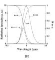
- An incandescent bulb has a radiation spectrum with excellent color rendering properties close to that of sunlight, and the conversion efficiency from the power of the incandescent bulb to light is 80% or more, but the wavelength component of the emitted light is as shown in FIG.
- the infrared radiation component is 90% or more (in the case of 3000K in FIG. 1).
- the conversion efficiency from the electric power of the incandescent bulb to visible light is as low as about 15 lm / W.
- the fluorescent lamp has a conversion efficiency from electric power to visible light of about 90 lm / W, which is larger than the incandescent bulb.
- the incandescent bulb is excellent in color rendering, but has a larger environmental load than the fluorescent lamp.
- Patent Documents 1 and 2 have a configuration in which an inert gas or a halogen gas is sealed inside a light bulb, whereby the evaporated filament material is halogenated and returned to the filament (halogen cycle) to increase the filament temperature. Proposed. These are generally called halogen lamps. Thereby, the effect of the increase in the power conversion efficiency to visible light and the extension of a filament lifetime is acquired. In this configuration, it is important to control the components of the sealed gas and the pressure in order to increase the efficiency and extend the life.
- Patent Documents 3-5 disclose a configuration in which an infrared reflecting coating is applied to the surface of a bulb glass so that infrared light emitted from the filament is reflected, returned to the filament, and absorbed. High efficiency is achieved by reheating the filament with infrared light reabsorbed by the filament.
- Patent Documents 6 to 9 propose a configuration in which a fine structure is produced in the filament itself, and the infrared radiation is suppressed and the ratio of visible light radiation is increased by the physical effect of the fine structure.
- JP-A-60-253146 Japanese Patent Laid-Open No. 62-10854 JP 59-58752 A JP-T 62-501109 JP 2000-123795 A JP 2001-519079 Japanese Patent Laid-Open No. 6-5263 JP-A-6-2167 JP 2006-205332 A
- Patent Documents 1 and 2 can achieve a life extension effect, but it is difficult to greatly improve the conversion efficiency, and the current efficiency is about 20 lm / W. is there.
- the technique of reflecting infrared radiation with an infrared reflecting coat and reabsorbing the filament is efficient because the reflectance of infrared light by the filament is as high as 70%. It does n’t happen well. Further, the infrared light reflected by the infrared reflective coating is absorbed by other parts other than the filament, such as the filament holding part and the base, and is not used for heating the filament. For this reason, it is difficult to greatly improve the conversion efficiency by this technology. Currently, the efficiency is about 20 lm / W.
- a technique for suppressing infrared radiation with a fine structure as in Patent Documents 6-9 is a report showing a radiation enhancement and suppression effect with respect to the wavelength of the extreme part of the infrared radiation spectrum as in Non-Patent Document 1.
- a fine microfabrication technique such as electron beam lithography is used for producing a fine structure, a light source using this is very expensive.
- the fine structure portion is melted and destroyed at a heating temperature of about 1000 ° C.
- An object of the present invention is to provide a light source device including a filament with high efficiency for converting electric power into visible light.
- a translucent airtight container a filament disposed in the translucent airtight container, and a lead wire for supplying a current to the filament
- the filament has a base formed of a metal material and a visible light absorption film covering the base, and the visible light absorption film is transparent in the infrared region.
- a featured light source device is provided.
- the light source device includes a translucent airtight container, a filament disposed in the translucent airtight container, and a lead wire for supplying a current to the filament,
- the filament includes a base formed of a metal material, and an infrared light reflection film covering the base.
- a light source device is provided.
- the infrared light radiation can be suppressed and the visible light radiation can be enhanced by the filament having a high reflectance in the infrared wavelength region and a low reflectance in the visible light wavelength region, the visible light luminous efficiency is improved.
- a light source device having a high level can be obtained.
- the graph which shows the wavelength dependence of the radiation energy of the conventional tungsten filament The graph which shows the relationship between the reflectance of the filament of this invention, an emissivity, and an emission spectrum. Sectional drawing of the filament of this embodiment.
- the filament of the present invention has a low reflectance close to 0% in the visible light region and a reflectance close to 100% in the infrared light region, as shown by the solid line in FIG. Specifically, it is desirable that the reflectance in the visible light region having a wavelength of 700 nm or less is a low reflectance of 20% or less, and the reflectance in the infrared light region is a high reflectance of 90% or more. Further, in the wavelength region between them, it is desirable that the reflectance monotonously increases from the short wavelength side to the long wavelength side as shown in FIG. This filament emits visible light with high efficiency when heated by current supply or the like. The principle will be described below based on Kirchhoff's law in blackbody radiation.
- Equation 1 The energy loss with respect to the input energy of the material (here, the filament) under conditions without natural convection heat transfer (for example, in a vacuum) is given by the following equation (1) in an equilibrium state.
- P (total) is the total input energy
- P (conduction) is the energy lost through the lead that supplies current to the filament
- P (radiation) is the temperature at which the filament is heated It is the energy lost by radiating light.
- the energy lost through the lead wire is only about 5%, and the remaining 95% or more is lost to the outside by light radiation. Almost all the power can be converted into light.
- the proportion of the visible light component is only about 10%, and most of it is the infrared radiated light component. Don't be.
- Equation (4) ⁇ ( ⁇ 0 ) has an emissivity of 0 from a long wavelength to a wavelength ⁇ 0 of visible light, and an emissivity of 1 in a region shorter than a certain wavelength ⁇ 0. It is a function that shows some step function behavior.
- the obtained radiation spectrum has a shape obtained by convolving the step function emissivity and the blackbody radiation spectrum, and the calculation result is a spectrum indicated by a broken line in FIG.
- the physical meaning of equation (4) is that the radiation loss is suppressed in the low temperature region where the input energy to the filament is small, and the P (radiation) term of equation (4) is 0, so the energy loss is Only the P (conduction), and the filament temperature rises very efficiently.
- the filament temperature is a high temperature
- the peak wavelength of black-body radiation spectrum is a temperature region as shorter than lambda 0, visible radiation as radiation spectrum that shows an energy input to the filament by a broken line in FIG. 2 As you come to lose.
- ⁇ ( ⁇ 0 ) in the equation (4) has an emissivity of 0 from a long wavelength to a wavelength ⁇ 0 where visible light is present as described above, and in the region of a shorter wavelength than the certain wavelength ⁇ 0 Is a material that is 1.
- a material has a reflectivity of 0 at a wavelength ⁇ 0 or less and a reflectivity of 1 in a wavelength region longer than the wavelength ⁇ 0 as shown by a solid line in FIG. 2 according to Kirchhoff's law of Equation (3). It becomes.
- the present invention provides a filament having a reflectance in the visible light region having a wavelength ⁇ 0 or less close to 0 and having a reflectance close to 1 in a longer wavelength region than the wavelength ⁇ 0 .
- the reflectance in the visible light region having a wavelength ⁇ 0 or less is a low reflectance of 20% or less
- the reflectance in a predetermined infrared light region having a wavelength longer than the wavelength ⁇ 0 is 90%.
- the visible light region having a wavelength ⁇ 0 or less is preferably 380 nm or less at a wavelength of 750 nm or less, and more preferably 380 nm or more at a wavelength of 700 nm or less.
- the predetermined infrared light region having a reflectance of 90% or more is preferably an infrared light region having a wavelength of 4000 nm or more, and when the reflectance is 90% or more in an infrared light region having a wavelength of 1000 nm or more. Since further improvement in luminous efficiency can be expected, it is more preferable. As long as the reflectance in the visible light region is 20% or less, the reflectance in a wavelength region shorter than the visible light region may exceed 20%.
- the reflectance changes from 20% or less to 90% or more between the visible light region where the reflectance is 20% or less and the infrared light region where the reflectance is 90% or more.
- the reflectance of this region may be less than 90%. Therefore, the reflectance in the wavelength region of the wavelength of 750 nm or more and 4000 nm or less may be greater than 20% and less than 90%.
- a conventional filament for a light source such as an incandescent bulb has a high temperature of 2000K to 3000K.
- the filament for light sources which shows the wavelength dependence of the above-mentioned reflectance at the high temperature of 2000K or more is provided.
- the inventors investigated conventional techniques that may obtain a material (filament) having the reflectance as described above, and found that the following methods (a) to (d) are known. I understood. However, when a detailed investigation is made, these materials cannot withstand temperatures of 1000 ° C. or higher, and reflect at the above-described reflection characteristics (wavelength ⁇ 0 700 nm or less in the visible light region) at temperatures of 2000 K or higher. It has been found that a reflectance of 20% or less and a reflectance of 90% or more in the infrared light region cannot be achieved. (a) A method of coating a chromium film, a nickel film, or the like on a substrate using a method such as electroplating. (For example, see G.
- the inventors use a high melting point material (melting point 2000K or higher) having a high infrared wavelength reflectivity as a filament base, a visible light absorbing film that reduces the reflectivity in the visible light region, and a red that increases the reflectivity of infrared light. At least one of the external light reflecting films is coated.
- a high melting point material melting point 2000K or higher
- a visible light absorbing film that reduces the reflectivity in the visible light region
- a red that increases the reflectivity of infrared light.
- At least one of the external light reflecting films is coated.
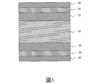
- FIG. 3 a filament having a structure in which a base material 10 is sequentially covered with an infrared reflection film 20, a visible light absorption film 30, and a visible light antireflection film 40 will be described.
- the high melting point material constituting the substrate is preferably a metal material having a melting point of 2000K or higher.
- HfC melting point 4160K
- TaC melting point 4150K
- ZrC melting point 3810K
- C melting point 3800K
- W melting point 3680K
- Re melting point 3453K
- Os melting point 3327K
- Ta melting point 3269K
- Of Mo molecular weight
- the shape of the substrate 10 may be any shape as long as it can be heated to a high temperature.
- the substrate 10 may have a linear shape, a rod shape, or a thin plate shape that can generate heat when supplied with current from a lead wire.
- the structure directly heated by methods other than electric current supply may be sufficient.
- the surface of the substrate is preferably mirror-polished.
- the surface of the substrate has a surface roughness (centerline average roughness Ra) of 1 ⁇ m or less, a maximum height (Rmax) of 10 ⁇ m or less, and a ten-point average roughness (Rz) of 10 ⁇ m or less.
- Ra centerline average roughness
- Rmax maximum height
- Rz ten-point average roughness
- at least one of the above is satisfied. This is because the emissivity of a metal material is generally related to the surface roughness, and as the surface roughness increases, the reflectance decreases as compared to a mirror-finished surface.
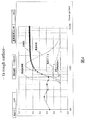
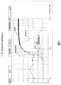
- FIG. 4 is a graph of the wavelength dependence of the reflectance before the Ta substrate 10 is mirror-finished (sand surface), and FIG. 5 is the wavelength dependence of the reflectance after the mirror polishing that satisfies the above-described surface roughness condition. Each graph is shown.
- the reflectance in the infrared region of the Ta base material after mirror polishing is improved by 10% or more compared to the reflectance before mirror polishing in FIG. Since the emission of long-wavelength infrared light decreases as the reflectivity increases, the luminous efficiency can be increased by mirror polishing the substrate 10. More specifically, as shown in FIGS.
- the Ta base material has a mirror surface reflectance (88%) compared to the sand surface reflectance (88%) in the infrared wavelength region of 1-10 ⁇ m. 98%) is improved by about 10%.
- the emissivity of the mirror-polished Ta base material 10 is reduced in the infrared wavelength region, as shown in FIGS. Therefore, when the visible light luminous efficiency is obtained in a temperature range of 2500 K, the visible light luminous efficiency of the mirror-polished Ta base 10 is compared with the visible light luminous efficiency 28.2 lm / W of the Ta base 10 on the sand surface. 52.2 lm / W, improved by 46%.
- the filament of the present invention is desired to be a high-temperature heat-resistant material having a reflectance as high as possible in the infrared wavelength region of 1-10 ⁇ m, it is desirable to mirror the surface of the substrate 10.
- the cause of the decrease in reflectance caused by the sand surface is multiple scattering and absorption of light caused by the sand surface structure.
- the infrared light reflection film 20 is disposed to increase the reflectance of the filament in the infrared light wavelength region by reflecting infrared light.
- the infrared light reflecting film 20 is a combination of a first layer 21 and a second layer 22 each made of a material that transmits infrared light, for example, a high heat resistant dielectric layer. Includes at least one pair.
- ⁇ of infrared light where the refractive index of the first layer 21 is n 1 , the thickness is d 1 , the refractive index of the second layer 22 is n 2 , and the thickness is d 2 , Formula (5) is satisfy
- the infrared light reflecting film 20 has a configuration in which a plurality of sets of two types of layers 21 and 22 are stacked as shown in FIG. .
- the center wavelength ⁇ of each set of reflections and reflecting infrared light of slightly different wavelengths in each of the stacked sets infrared light in a wide wavelength range as a whole of the infrared light reflection film 20 can be obtained.
- some sets of the plurality of sets may have the same center wavelength.
- two sets may be configured to reflect the same center wavelength.
- the first layer 21 is an MgO layer
- the second layer 22 is an SiC layer.
- Radiation from a black body at a temperature of 2500 K has a peak at an infrared wavelength of about 1200 nm. Therefore, by selecting a wavelength around this peak and enhancing reflection in this wavelength band, the luminous efficiency can be improved. it can.
- the first layer 21 and the second layer 22 are made of SiO 2 , MgO, ZrO 2 , Y 2 O 3 , 6H—SiC (hexagonal SiC), GaN, 3C—SiC (cubic SiC), HfO.
- the present invention is limited to this configuration.
- the combination of the materials of the first layer 21 and the second layer 22 may be different for each set.
- the difference in refractive index between the first layer 21 and the second layer 22 is preferably 0.1 or more because good reflectance characteristics can be obtained.
- the greater the difference in refractive index the wider the wavelength range that can be reflected by one set of the first layer 21 and the second layer 22, and the total number of thin film stacks can be reduced. It is desirable.
- a visible light absorbing film 30 is disposed on the infrared light reflecting film 20.
- the visible light absorbing film 30 is a film that is transparent to infrared light and has a high visible light absorptance, and absorbs visible light, thereby reducing the reflectance in the visible light wavelength region of the filament.
- the visible light absorbing film 30 is made of a material transparent to the infrared light region, for example, a material obtained by adding metal fine particles to a high heat resistant dielectric, or a material obtained by adding impurities to a material transparent to the infrared light region. .
- visible light can be absorbed by the action of local light absorption by the metal fine particles.
- a typical example of utilizing the localized light absorption effect by metal fine particles is a stained glass of a church. Since the absorption wavelength and absorption amount in the visible light region can be controlled in accordance with the type and particle size of the metal dispersed in the glass, various absorption bands can be formed like stained glass. For example, by changing the particle size of Au fine particles from 2 nm to 5 nm, the stained glass color can be changed from pink to deep green. This is due to a change in transmitted light (complementary color) due to the local resonance absorption effect of the. That is, when the particle size is small, short wavelength light is absorbed, and as the particle size increases, long wavelength light is absorbed. Absorption in which metal fine particles are added to a material transparent in the infrared region is also based on this principle.
- the particle size of the metal fine particles is desirably 2 nm or more and 5 ⁇ m or less.
- the amount of metal fine particles added is preferably 0.0001% or more and 10% or less.
- the metal fine particles desirably have a melting point of 2000 K or higher, which is the temperature at which the filament emits light.
- a material obtained by adding impurities to a transparent material in the infrared light region can absorb visible light with the same physical effect as the phosphor material. That is, the absorption reflects the energy level created by the atoms (ions) added to the transparent material in the infrared light region.
- the absorption reflects the energy level created by the atoms (ions) added to the transparent material in the infrared light region.
- an element added to a material transparent in the infrared light region is dispersed atomically (ionic) in contrast to the above-described example of the metal fine particles. It is necessary to be.
- the impurity concentration is preferably 0.0001% or more and 10% or less.
- the visible light absorption film 30 a SiC film to which metal fine particles or impurities are added can be used.
- the film thickness of the visible light absorbing film 30 is designed so that the required transmittance can be obtained.
- the thickness d necessary for setting the transmittance to 0.35 is 200 nm.
- a method for forming the visible light absorbing film 30 to which the metal fine particles are added a method of co-evaporating when forming a transparent dielectric (SiC) film on the infrared light constituting the film 30 by vapor deposition or the above infrared
- SiC transparent dielectric
- a method of ion implantation after coating a transparent dielectric film on light can be used.
- SiC and a metal fine particle material Ta are prepared, and the metal fine particle material is mixed in SiC at a ratio of 0.0001% to 10%, The mixed material is heated with an electron beam and simultaneously deposited on the substrate. Thereafter, a method of firing and growing metal fine crystal crystals in a transparent dielectric is used.
- SiC is prepared as a deposition source, an SiC film is formed, Ta metal ions, which are fine metal particle materials, are implanted using an ion implantation apparatus, and then fired to form a transparent dielectric. A method of growing crystals of metal fine particles in the inside is used.
- a visible light antireflection film 40 is disposed on the visible light absorbing film 30.
- the visible light antireflection film 40 is a film that acts to reduce the reflectance of visible light.
- the visible light antireflection film 40 is transparent to visible light, visible light reflected by the surface of the visible light antireflection film 40, and the lower surface (visible light absorbing film 30) that passes through the visible light antireflection film 40.
- the visible light reflectivity of the filament is reduced by canceling the visible light reflected at the interface between the filament and the visible light.
- the film thickness of the visible light antireflection film is designed to an appropriate value by calculation according to the refractive index, or by experiment or simulation.
- the film thickness is such that the optical path length for visible light ( ⁇ / n 0, where n 0 is the refractive index of the visible light antireflection film) is about 1 ⁇ 4 wavelength.
- the film thickness is designed by experiment or simulation, for example, by varying the film thickness, obtaining the film thickness dependence of the reflectance of the filament, and obtaining the film thickness with the lowest reflectivity with respect to the wavelength of the entire visible light Is used.
- the visible light antireflection film 40 is formed of a dielectric film having a melting point of 2000K or higher.
- a dielectric film having a melting point of 2000K or higher for example, any one of a metal oxide film, a nitride film, a carbide film, and a boride film having a melting point of 2000K or higher is used.
- the visible light antireflection film 40 for example, an MgO film is coated to about 80 nm.
- the optical film thickness of the MgO thin film becomes a quarter of this wavelength at a wavelength of 550 nm, the reflectance at a wavelength of 550 nm can be reduced by optical interference.
- the method for forming the infrared reflection film 20 and the visible light antireflection film 40 various methods such as an electron beam evaporation method, a sputtering method, and a CVD method can be used. After the film formation, it is preferable to perform an annealing treatment in the temperature range of 1500 ° C. to 2500 ° C. in order to improve the adhesion with the interface of the substrate 10 and the film quality (crystallinity, optical characteristics, etc.).
- the filament of the present invention suppresses the reflectance in the visible light region to be low by covering the base material 10 with the infrared light reflection film 20, the visible light absorption film 30, and the visible light antireflection film 40 in this order. It is possible to obtain a reflection characteristic in which the reflectance in the infrared light region is increased.
- the substrate is made of Ta
- the infrared light reflection film 20 is made of various combinations of nine types of materials for the first layer 21 and the second layer 22 described later. A filament changed to is produced.
- the visible light absorbing film 30 is made of SiC added with metal fine particles of Ta (particle size: 3 nm) at a concentration of 0.1%.
- the film thickness of the visible light absorbing film 30 is approximately 200 nm.
- an MgO film is used, and the film thickness is 80 nm.
- the substrate 10 is manufactured by a known process such as sintering or drawing of a metal material.
- the base is formed in a desired shape such as a wire, a bar, or a thin plate.
- a substrate manufactured by a process such as sintering or drawing is polished with a plurality of kinds of diamond abrasive grains, the center line average roughness Ra is 1 ⁇ m or less, the maximum height (Rmax) is 10 ⁇ m or less, and the ten-point average roughness ( Rz) is processed into a mirror surface of 10 ⁇ m or less.
- the infrared light reflection film 20 is composed of the second layer 22 / the first layer 21 in which two sets of the same film structure are alternately formed using a SiC / MgO material. It is set as the structure (52 layers in total with a single layer) which laminated
- the central wavelength ⁇ of each set is designed so as to reflect infrared light having a wavelength of 700 nm to 10 ⁇ m with a total of 52 layers.
- the second layer 22 / first layer 21 is made of SiC / ZrO 2 , SiC / Y 2 O 3 , SiC / HfO 2 , SiC / Lu 2 O 3 , SiC / Yb 2 O 3. , SiC / SiO 2 , HfO 2 / SiO 2 , Lu 2 O 3 / SiO 2 respectively.
- the number of layers is the same as in the first embodiment.
- FIG. 7 shows the reflection characteristics (the reflectance at 550 nm and the reflectance at 1 ⁇ m) obtained by the infrared light reflecting films 20 of the first to ninth embodiments, and the wavelength at which the reflectance becomes 50% (Cut-off wavelength). Is shown.
- the filament provided with the infrared light reflecting film 20, the visible light absorbing film 30, and the visible light antireflection layer 40 on the mirror-polished Ta substrate 10 of each of the first to ninth embodiments was obtained by simulation.
- the visible light luminous efficiency (2500K) is shown.
- the visible light beam efficiencies of the filaments of Embodiments 1 to 9 are as high as 75.4 to 113.0 lm / W, and the visible light beam efficiency of the mirror-polished Ta10 substrate is 52.2 lm. It is higher than / W.
- the filaments of Embodiments 1 to 9 can improve the visible light luminous efficiency.
- FIG. 8 shows the reflectance and emissivity of the filament of the first embodiment.
- the infrared light reflecting film (SiC / MgO) 20 by providing the infrared light reflecting film (SiC / MgO) 20, the visible light absorbing film 30, and the visible light antireflection layer 40 on the mirror-polished Ta substrate 10 as in the first embodiment.
- the reflection characteristic changes sharply from approximately 0.1 to approximately 1 at a wavelength of 600 to 700 nm, the reflectance in the visible light region is as low as 0 to 0.1, and the infrared light region is It can be confirmed that a filament close to 1 is obtained in a wide range of reflectance. Therefore, it can be seen that the emissivity (2500 K) in the infrared light region can be reduced, and the high visible light luminous efficiency of 103.2 lm / W as described above can be obtained.
- FIG. 9 shows a cut-away cross-sectional view of an incandescent bulb using the filament of this embodiment.
- the incandescent lamp 1 includes a translucent airtight container 2, a filament 3 disposed inside the translucent airtight container 2, and a pair of lead wires that are electrically connected to both ends of the filament 3 and support the filament 3. 4 and 5.
- the translucent airtight container 2 is constituted by, for example, a glass bulb.
- the inside of the translucent airtight container 2 is in a high vacuum state of 10 ⁇ 1 to 10 ⁇ 6 Pa.
- a base 9 is joined to the sealing portion of the translucent airtight container 2.
- the base 9 includes a side electrode 6, a center electrode 7, and an insulating portion 8 that insulates the side electrode 6 from the center electrode 7.
- the end portion of the lead wire 4 is electrically connected to the side electrode 6, and the end portion of the lead wire 5 is electrically connected to the center electrode 7.
- the filament 3 has a structure in which a wire-shaped filament is wound in a spiral shape.
- the filament 3 includes the infrared reflection film 20, the visible light absorption film 30, and the visible light antireflection film 40 on the base, the reflectance in the infrared wavelength region is high and the reflectance in the visible light region is low. .
- high visible light luminous efficiency luminous efficiency
- the reflectance of the filament surface is improved by mechanical polishing.
- the present invention is not limited to mechanical polishing, and other methods can be used as long as the reflectance of the filament surface can be improved. It is. For example, wet or dry etching, a method of contacting a smooth die during drawing, forging or rolling can be employed.
- the filament of the present invention is used as a filament of an incandescent bulb, but it can also be used other than an incandescent bulb.
- the structure of the visible light absorption film 30 and the visible light antireflection film 40 is designed for heaters by redesigning the film thickness, material, and impurity addition concentration to shift from the visible region to the gold infrared region. It can be employed as an electric wire, a welding wire, a thermionic emission electron source (X-ray tube, electron microscope, etc.) and the like. Also in this case, since the filament can be efficiently heated to a high temperature with a small amount of input power due to the suppression effect of infrared light radiation (particularly suppression of long-wavelength infrared radiation), energy efficiency can be improved. .
Landscapes
- Engineering & Computer Science (AREA)
- Manufacturing & Machinery (AREA)
- Optical Elements Other Than Lenses (AREA)
- Optical Filters (AREA)
Priority Applications (1)
| Application Number | Priority Date | Filing Date | Title |
|---|---|---|---|
| US14/368,783 US9214330B2 (en) | 2011-12-26 | 2012-12-20 | Light source device and filament |
Applications Claiming Priority (2)
| Application Number | Priority Date | Filing Date | Title |
|---|---|---|---|
| JP2011-284068 | 2011-12-26 | ||
| JP2011284068A JP2013134875A (ja) | 2011-12-26 | 2011-12-26 | 白熱電球、および、フィラメント |
Publications (1)
| Publication Number | Publication Date |
|---|---|
| WO2013099759A1 true WO2013099759A1 (ja) | 2013-07-04 |
Family
ID=48697248
Family Applications (1)
| Application Number | Title | Priority Date | Filing Date |
|---|---|---|---|
| PCT/JP2012/083088 Ceased WO2013099759A1 (ja) | 2011-12-26 | 2012-12-20 | 光源装置、および、フィラメント |
Country Status (3)
| Country | Link |
|---|---|
| US (1) | US9214330B2 (enExample) |
| JP (1) | JP2013134875A (enExample) |
| WO (1) | WO2013099759A1 (enExample) |
Cited By (2)
| Publication number | Priority date | Publication date | Assignee | Title |
|---|---|---|---|---|
| WO2016028743A1 (en) * | 2014-08-22 | 2016-02-25 | Ut-Battelle, Llc | Infrared signal generation from ac induction field heating of graphite foam |
| US10284021B2 (en) | 2017-08-14 | 2019-05-07 | Ut-Battelle, Llc | Lighting system with induction power supply |
Families Citing this family (8)
| Publication number | Priority date | Publication date | Assignee | Title |
|---|---|---|---|---|
| JP6189682B2 (ja) * | 2013-08-29 | 2017-08-30 | スタンレー電気株式会社 | 白熱電球およびフィラメント |
| JP6253313B2 (ja) * | 2013-08-30 | 2017-12-27 | スタンレー電気株式会社 | フィラメント、および、それを用いた光源 |
| JP6302651B2 (ja) * | 2013-11-28 | 2018-03-28 | スタンレー電気株式会社 | 白熱電球およびフィラメント |
| JP6371075B2 (ja) * | 2014-02-21 | 2018-08-08 | スタンレー電気株式会社 | フィラメント |
| US9739501B2 (en) | 2014-08-22 | 2017-08-22 | Ut-Battelle, Llc | AC induction field heating of graphite foam |
| US11131502B2 (en) | 2017-08-14 | 2021-09-28 | Ut-Battelle, Llc | Heating system with induction power supply and electromagnetic acoustic transducer with induction power supply |
| WO2019113020A1 (en) * | 2017-12-04 | 2019-06-13 | Rensselaer Polytechnic Institute | Membrane-based selective surface-integrated water desalination system |
| TWI825187B (zh) * | 2018-10-09 | 2023-12-11 | 日商東京威力科創股份有限公司 | 氮化物半導體膜之形成方法 |
Citations (9)
| Publication number | Priority date | Publication date | Assignee | Title |
|---|---|---|---|---|
| JPS5572357A (en) * | 1978-11-24 | 1980-05-31 | Kiyoshi Hajikano | Filament |
| JPS56145652A (en) * | 1980-04-11 | 1981-11-12 | Rikuun Denki Kk | Bulb filament |
| JPH10289689A (ja) * | 1997-04-11 | 1998-10-27 | Sony Corp | ランプ電極の構造 |
| JP2000215858A (ja) * | 1999-01-26 | 2000-08-04 | Stanley Electric Co Ltd | 波長選択性反射膜付電球 |
| JP2000260398A (ja) * | 1999-03-10 | 2000-09-22 | Stanley Electric Co Ltd | 赤外線反射膜付き白熱電球 |
| JP2003168399A (ja) * | 2001-12-03 | 2003-06-13 | Ushio Inc | 白熱電球 |
| JP2006520074A (ja) * | 2003-03-06 | 2006-08-31 | チ・エレ・エッフェ・ソシエタ・コンソルティーレ・ペル・アチオニ | 白熱光源用の高性能エミッタ |
| JP2010272435A (ja) * | 2009-05-25 | 2010-12-02 | Toshiba Lighting & Technology Corp | 高圧放電ランプおよび照明装置 |
| JP2011124206A (ja) * | 2009-11-11 | 2011-06-23 | Stanley Electric Co Ltd | 可視光源 |
Family Cites Families (20)
| Publication number | Priority date | Publication date | Assignee | Title |
|---|---|---|---|---|
| US3973155A (en) * | 1975-01-31 | 1976-08-03 | Westinghouse Electric Corporation | Incandescent source of visible radiations |
| US4361598A (en) * | 1979-08-10 | 1982-11-30 | Westinghouse Electric Corp. | Polymerized solutions for depositing optical oxide coatings |
| JPS5958752A (ja) | 1982-09-28 | 1984-04-04 | 東芝ライテック株式会社 | 白熱電球 |
| JPS60253146A (ja) | 1984-05-29 | 1985-12-13 | 東芝ライテック株式会社 | ハロゲン電球 |
| JPS62501109A (ja) | 1984-10-23 | 1987-04-30 | デユロ テスト コ−ポレ−シヨン | 透明熱反射鏡およびそれを使用した電球 |
| JPS6210854A (ja) | 1985-06-26 | 1987-01-19 | スタンレー電気株式会社 | 高効率白熱電球 |
| JPH062167A (ja) | 1992-06-19 | 1994-01-11 | Matsushita Electric Works Ltd | 微細穴を有する金属体の製造方法およびランプ用発光体の製造方法 |
| JPH065263A (ja) | 1992-06-19 | 1994-01-14 | Matsushita Electric Works Ltd | 微細穴を有する金属体の製造方法およびランプ用発光体の製造方法 |
| US5955839A (en) | 1997-03-26 | 1999-09-21 | Quantum Vision, Inc. | Incandescent microcavity lightsource having filament spaced from reflector at node of wave emitted |
| JP2000123795A (ja) | 1998-10-09 | 2000-04-28 | Stanley Electric Co Ltd | 赤外線反射膜付白熱電球 |
| JP2002222638A (ja) * | 2001-01-26 | 2002-08-09 | Oshino Denki Seisakusho:Kk | ガス等のセンサー・濃度検知器などに用いる赤外線放射光源 |
| GB0216931D0 (en) * | 2002-07-20 | 2002-08-28 | Bae Systems Plc | Incandescent lighting |
| ITTO20030167A1 (it) * | 2003-03-06 | 2004-09-07 | Fiat Ricerche | Procedimento per la realizzazione di emettitori nano-strutturati per sorgenti di luce ad incandescenza. |
| JP2006205332A (ja) | 2005-01-31 | 2006-08-10 | Towa Corp | 微細構造体、その製造方法、その製造に使用されるマスター型、及び発光機構 |
| US7851985B2 (en) | 2006-03-31 | 2010-12-14 | General Electric Company | Article incorporating a high temperature ceramic composite for selective emission |
| US7965026B2 (en) * | 2009-06-25 | 2011-06-21 | General Electric Company | Lamp with IR suppressing composite |
| WO2011057410A1 (en) * | 2009-11-12 | 2011-05-19 | Opalux Incorporated | Photonic crystal incandescent light source |
| JP5506514B2 (ja) * | 2010-04-07 | 2014-05-28 | スタンレー電気株式会社 | 赤外光源 |
| US9070851B2 (en) * | 2010-09-24 | 2015-06-30 | Seoul Semiconductor Co., Ltd. | Wafer-level light emitting diode package and method of fabricating the same |
| TWI447441B (zh) * | 2010-11-08 | 2014-08-01 | Ind Tech Res Inst | 紅外光阻隔多層膜結構 |
-
2011
- 2011-12-26 JP JP2011284068A patent/JP2013134875A/ja active Pending
-
2012
- 2012-12-20 WO PCT/JP2012/083088 patent/WO2013099759A1/ja not_active Ceased
- 2012-12-20 US US14/368,783 patent/US9214330B2/en not_active Expired - Fee Related
Patent Citations (9)
| Publication number | Priority date | Publication date | Assignee | Title |
|---|---|---|---|---|
| JPS5572357A (en) * | 1978-11-24 | 1980-05-31 | Kiyoshi Hajikano | Filament |
| JPS56145652A (en) * | 1980-04-11 | 1981-11-12 | Rikuun Denki Kk | Bulb filament |
| JPH10289689A (ja) * | 1997-04-11 | 1998-10-27 | Sony Corp | ランプ電極の構造 |
| JP2000215858A (ja) * | 1999-01-26 | 2000-08-04 | Stanley Electric Co Ltd | 波長選択性反射膜付電球 |
| JP2000260398A (ja) * | 1999-03-10 | 2000-09-22 | Stanley Electric Co Ltd | 赤外線反射膜付き白熱電球 |
| JP2003168399A (ja) * | 2001-12-03 | 2003-06-13 | Ushio Inc | 白熱電球 |
| JP2006520074A (ja) * | 2003-03-06 | 2006-08-31 | チ・エレ・エッフェ・ソシエタ・コンソルティーレ・ペル・アチオニ | 白熱光源用の高性能エミッタ |
| JP2010272435A (ja) * | 2009-05-25 | 2010-12-02 | Toshiba Lighting & Technology Corp | 高圧放電ランプおよび照明装置 |
| JP2011124206A (ja) * | 2009-11-11 | 2011-06-23 | Stanley Electric Co Ltd | 可視光源 |
Cited By (3)
| Publication number | Priority date | Publication date | Assignee | Title |
|---|---|---|---|---|
| WO2016028743A1 (en) * | 2014-08-22 | 2016-02-25 | Ut-Battelle, Llc | Infrared signal generation from ac induction field heating of graphite foam |
| US9906078B2 (en) | 2014-08-22 | 2018-02-27 | Ut-Battelle, Llc | Infrared signal generation from AC induction field heating of graphite foam |
| US10284021B2 (en) | 2017-08-14 | 2019-05-07 | Ut-Battelle, Llc | Lighting system with induction power supply |
Also Published As
| Publication number | Publication date |
|---|---|
| JP2013134875A (ja) | 2013-07-08 |
| US9214330B2 (en) | 2015-12-15 |
| US20140346944A1 (en) | 2014-11-27 |
Similar Documents
| Publication | Publication Date | Title |
|---|---|---|
| WO2013099759A1 (ja) | 光源装置、および、フィラメント | |
| JP6223186B2 (ja) | 光源装置、および、フィラメント | |
| JP5689934B2 (ja) | 光源 | |
| US8267547B2 (en) | Incandescent illumination system incorporating an infrared-reflective shroud | |
| JP5964581B2 (ja) | 白熱電球 | |
| JP6153734B2 (ja) | 光源装置 | |
| JP2015050001A (ja) | 近赤外ヒーター | |
| JP6134194B2 (ja) | フィラメント、光源装置、および、フィラメントの製造方法 | |
| JP6253313B2 (ja) | フィラメント、および、それを用いた光源 | |
| JP6239839B2 (ja) | 光源装置、および、フィラメント | |
| JP2016015260A (ja) | フィラメント、それを用いた光源、および、フィラメントの製造方法 | |
| JP6255189B2 (ja) | 発光体、光源装置、熱放射装置、熱電子放出装置および白熱電球 | |
| JP6189682B2 (ja) | 白熱電球およびフィラメント | |
| JP2014112477A (ja) | 光源装置およびフィラメント | |
| JP6302651B2 (ja) | 白熱電球およびフィラメント | |
| JP6708439B2 (ja) | 発光体、フィラメント、フィラメントを用いた装置、および、白熱電球 | |
| JP6625902B2 (ja) | 発光体、フィラメント、フィラメントを用いた装置、および、白熱電球 | |
| JP2015156314A (ja) | フィラメント、それを用いた光源およびヒーター | |
| WO2012088343A1 (en) | Incandescent illumination system incorporation an infrared-reflective shroud | |
| JP2017157333A (ja) | 発光体、フィラメント、フィラメントを用いた装置、および、白熱電球 |
Legal Events
| Date | Code | Title | Description |
|---|---|---|---|
| 121 | Ep: the epo has been informed by wipo that ep was designated in this application |
Ref document number: 12862447 Country of ref document: EP Kind code of ref document: A1 |
|
| WWE | Wipo information: entry into national phase |
Ref document number: 14368783 Country of ref document: US |
|
| NENP | Non-entry into the national phase |
Ref country code: DE |
|
| 122 | Ep: pct application non-entry in european phase |
Ref document number: 12862447 Country of ref document: EP Kind code of ref document: A1 |