WO2013099759A1 - Light source device and filament - Google Patents
Light source device and filament Download PDFInfo
- Publication number
- WO2013099759A1 WO2013099759A1 PCT/JP2012/083088 JP2012083088W WO2013099759A1 WO 2013099759 A1 WO2013099759 A1 WO 2013099759A1 JP 2012083088 W JP2012083088 W JP 2012083088W WO 2013099759 A1 WO2013099759 A1 WO 2013099759A1
- Authority
- WO
- WIPO (PCT)
- Prior art keywords
- source device
- light source
- visible light
- filament
- light
- Prior art date
Links
Images


Classifications
-
- H—ELECTRICITY
- H01—ELECTRIC ELEMENTS
- H01K—ELECTRIC INCANDESCENT LAMPS
- H01K1/00—Details
- H01K1/26—Screens; Filters
-
- H—ELECTRICITY
- H01—ELECTRIC ELEMENTS
- H01K—ELECTRIC INCANDESCENT LAMPS
- H01K1/00—Details
- H01K1/02—Incandescent bodies
- H01K1/04—Incandescent bodies characterised by the material thereof
-
- H—ELECTRICITY
- H01—ELECTRIC ELEMENTS
- H01K—ELECTRIC INCANDESCENT LAMPS
- H01K1/00—Details
- H01K1/02—Incandescent bodies
- H01K1/04—Incandescent bodies characterised by the material thereof
- H01K1/10—Bodies of metal or carbon combined with other substance
-
- H—ELECTRICITY
- H01—ELECTRIC ELEMENTS
- H01K—ELECTRIC INCANDESCENT LAMPS
- H01K3/00—Apparatus or processes adapted to the manufacture, installing, removal, or maintenance of incandescent lamps or parts thereof
- H01K3/02—Manufacture of incandescent bodies
Definitions
- the present invention relates to a light source filament with improved energy utilization efficiency, and more particularly to a light source device using the filament, particularly an incandescent bulb, near infrared rays, and a thermionic emission source.
- Incandescent light bulbs are widely used that emit light by flowing current through a tungsten filament or the like.
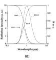
- An incandescent bulb has a radiation spectrum with excellent color rendering properties close to that of sunlight, and the conversion efficiency from the power of the incandescent bulb to light is 80% or more, but the wavelength component of the emitted light is as shown in FIG.
- the infrared radiation component is 90% or more (in the case of 3000K in FIG. 1).
- the conversion efficiency from the electric power of the incandescent bulb to visible light is as low as about 15 lm / W.
- the fluorescent lamp has a conversion efficiency from electric power to visible light of about 90 lm / W, which is larger than the incandescent bulb.
- the incandescent bulb is excellent in color rendering, but has a larger environmental load than the fluorescent lamp.
- Patent Documents 1 and 2 have a configuration in which an inert gas or a halogen gas is sealed inside a light bulb, whereby the evaporated filament material is halogenated and returned to the filament (halogen cycle) to increase the filament temperature. Proposed. These are generally called halogen lamps. Thereby, the effect of the increase in the power conversion efficiency to visible light and the extension of a filament lifetime is acquired. In this configuration, it is important to control the components of the sealed gas and the pressure in order to increase the efficiency and extend the life.
- Patent Documents 3-5 disclose a configuration in which an infrared reflecting coating is applied to the surface of a bulb glass so that infrared light emitted from the filament is reflected, returned to the filament, and absorbed. High efficiency is achieved by reheating the filament with infrared light reabsorbed by the filament.
- Patent Documents 6 to 9 propose a configuration in which a fine structure is produced in the filament itself, and the infrared radiation is suppressed and the ratio of visible light radiation is increased by the physical effect of the fine structure.
- JP-A-60-253146 Japanese Patent Laid-Open No. 62-10854 JP 59-58752 A JP-T 62-501109 JP 2000-123795 A JP 2001-519079 Japanese Patent Laid-Open No. 6-5263 JP-A-6-2167 JP 2006-205332 A
- Patent Documents 1 and 2 can achieve a life extension effect, but it is difficult to greatly improve the conversion efficiency, and the current efficiency is about 20 lm / W. is there.
- the technique of reflecting infrared radiation with an infrared reflecting coat and reabsorbing the filament is efficient because the reflectance of infrared light by the filament is as high as 70%. It does n’t happen well. Further, the infrared light reflected by the infrared reflective coating is absorbed by other parts other than the filament, such as the filament holding part and the base, and is not used for heating the filament. For this reason, it is difficult to greatly improve the conversion efficiency by this technology. Currently, the efficiency is about 20 lm / W.
- a technique for suppressing infrared radiation with a fine structure as in Patent Documents 6-9 is a report showing a radiation enhancement and suppression effect with respect to the wavelength of the extreme part of the infrared radiation spectrum as in Non-Patent Document 1.
- a fine microfabrication technique such as electron beam lithography is used for producing a fine structure, a light source using this is very expensive.
- the fine structure portion is melted and destroyed at a heating temperature of about 1000 ° C.
- An object of the present invention is to provide a light source device including a filament with high efficiency for converting electric power into visible light.
- a translucent airtight container a filament disposed in the translucent airtight container, and a lead wire for supplying a current to the filament
- the filament has a base formed of a metal material and a visible light absorption film covering the base, and the visible light absorption film is transparent in the infrared region.
- a featured light source device is provided.
- the light source device includes a translucent airtight container, a filament disposed in the translucent airtight container, and a lead wire for supplying a current to the filament,
- the filament includes a base formed of a metal material, and an infrared light reflection film covering the base.
- a light source device is provided.
- the infrared light radiation can be suppressed and the visible light radiation can be enhanced by the filament having a high reflectance in the infrared wavelength region and a low reflectance in the visible light wavelength region, the visible light luminous efficiency is improved.
- a light source device having a high level can be obtained.
- the graph which shows the wavelength dependence of the radiation energy of the conventional tungsten filament The graph which shows the relationship between the reflectance of the filament of this invention, an emissivity, and an emission spectrum. Sectional drawing of the filament of this embodiment.
- the filament of the present invention has a low reflectance close to 0% in the visible light region and a reflectance close to 100% in the infrared light region, as shown by the solid line in FIG. Specifically, it is desirable that the reflectance in the visible light region having a wavelength of 700 nm or less is a low reflectance of 20% or less, and the reflectance in the infrared light region is a high reflectance of 90% or more. Further, in the wavelength region between them, it is desirable that the reflectance monotonously increases from the short wavelength side to the long wavelength side as shown in FIG. This filament emits visible light with high efficiency when heated by current supply or the like. The principle will be described below based on Kirchhoff's law in blackbody radiation.
- Equation 1 The energy loss with respect to the input energy of the material (here, the filament) under conditions without natural convection heat transfer (for example, in a vacuum) is given by the following equation (1) in an equilibrium state.
- P (total) is the total input energy
- P (conduction) is the energy lost through the lead that supplies current to the filament
- P (radiation) is the temperature at which the filament is heated It is the energy lost by radiating light.
- the energy lost through the lead wire is only about 5%, and the remaining 95% or more is lost to the outside by light radiation. Almost all the power can be converted into light.
- the proportion of the visible light component is only about 10%, and most of it is the infrared radiated light component. Don't be.
- Equation (4) ⁇ ( ⁇ 0 ) has an emissivity of 0 from a long wavelength to a wavelength ⁇ 0 of visible light, and an emissivity of 1 in a region shorter than a certain wavelength ⁇ 0. It is a function that shows some step function behavior.
- the obtained radiation spectrum has a shape obtained by convolving the step function emissivity and the blackbody radiation spectrum, and the calculation result is a spectrum indicated by a broken line in FIG.
- the physical meaning of equation (4) is that the radiation loss is suppressed in the low temperature region where the input energy to the filament is small, and the P (radiation) term of equation (4) is 0, so the energy loss is Only the P (conduction), and the filament temperature rises very efficiently.
- the filament temperature is a high temperature
- the peak wavelength of black-body radiation spectrum is a temperature region as shorter than lambda 0, visible radiation as radiation spectrum that shows an energy input to the filament by a broken line in FIG. 2 As you come to lose.
- ⁇ ( ⁇ 0 ) in the equation (4) has an emissivity of 0 from a long wavelength to a wavelength ⁇ 0 where visible light is present as described above, and in the region of a shorter wavelength than the certain wavelength ⁇ 0 Is a material that is 1.
- a material has a reflectivity of 0 at a wavelength ⁇ 0 or less and a reflectivity of 1 in a wavelength region longer than the wavelength ⁇ 0 as shown by a solid line in FIG. 2 according to Kirchhoff's law of Equation (3). It becomes.
- the present invention provides a filament having a reflectance in the visible light region having a wavelength ⁇ 0 or less close to 0 and having a reflectance close to 1 in a longer wavelength region than the wavelength ⁇ 0 .
- the reflectance in the visible light region having a wavelength ⁇ 0 or less is a low reflectance of 20% or less
- the reflectance in a predetermined infrared light region having a wavelength longer than the wavelength ⁇ 0 is 90%.
- the visible light region having a wavelength ⁇ 0 or less is preferably 380 nm or less at a wavelength of 750 nm or less, and more preferably 380 nm or more at a wavelength of 700 nm or less.
- the predetermined infrared light region having a reflectance of 90% or more is preferably an infrared light region having a wavelength of 4000 nm or more, and when the reflectance is 90% or more in an infrared light region having a wavelength of 1000 nm or more. Since further improvement in luminous efficiency can be expected, it is more preferable. As long as the reflectance in the visible light region is 20% or less, the reflectance in a wavelength region shorter than the visible light region may exceed 20%.
- the reflectance changes from 20% or less to 90% or more between the visible light region where the reflectance is 20% or less and the infrared light region where the reflectance is 90% or more.
- the reflectance of this region may be less than 90%. Therefore, the reflectance in the wavelength region of the wavelength of 750 nm or more and 4000 nm or less may be greater than 20% and less than 90%.
- a conventional filament for a light source such as an incandescent bulb has a high temperature of 2000K to 3000K.
- the filament for light sources which shows the wavelength dependence of the above-mentioned reflectance at the high temperature of 2000K or more is provided.
- the inventors investigated conventional techniques that may obtain a material (filament) having the reflectance as described above, and found that the following methods (a) to (d) are known. I understood. However, when a detailed investigation is made, these materials cannot withstand temperatures of 1000 ° C. or higher, and reflect at the above-described reflection characteristics (wavelength ⁇ 0 700 nm or less in the visible light region) at temperatures of 2000 K or higher. It has been found that a reflectance of 20% or less and a reflectance of 90% or more in the infrared light region cannot be achieved. (a) A method of coating a chromium film, a nickel film, or the like on a substrate using a method such as electroplating. (For example, see G.
- the inventors use a high melting point material (melting point 2000K or higher) having a high infrared wavelength reflectivity as a filament base, a visible light absorbing film that reduces the reflectivity in the visible light region, and a red that increases the reflectivity of infrared light. At least one of the external light reflecting films is coated.
- a high melting point material melting point 2000K or higher
- a visible light absorbing film that reduces the reflectivity in the visible light region
- a red that increases the reflectivity of infrared light.
- At least one of the external light reflecting films is coated.
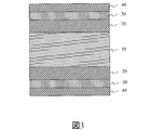
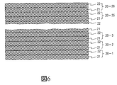
- FIG. 3 a filament having a structure in which a base material 10 is sequentially covered with an infrared reflection film 20, a visible light absorption film 30, and a visible light antireflection film 40 will be described.
- the high melting point material constituting the substrate is preferably a metal material having a melting point of 2000K or higher.
- HfC melting point 4160K
- TaC melting point 4150K
- ZrC melting point 3810K
- C melting point 3800K
- W melting point 3680K
- Re melting point 3453K
- Os melting point 3327K
- Ta melting point 3269K
- Of Mo molecular weight
- the shape of the substrate 10 may be any shape as long as it can be heated to a high temperature.
- the substrate 10 may have a linear shape, a rod shape, or a thin plate shape that can generate heat when supplied with current from a lead wire.
- the structure directly heated by methods other than electric current supply may be sufficient.
- the surface of the substrate is preferably mirror-polished.
- the surface of the substrate has a surface roughness (centerline average roughness Ra) of 1 ⁇ m or less, a maximum height (Rmax) of 10 ⁇ m or less, and a ten-point average roughness (Rz) of 10 ⁇ m or less.
- Ra centerline average roughness
- Rmax maximum height
- Rz ten-point average roughness
- at least one of the above is satisfied. This is because the emissivity of a metal material is generally related to the surface roughness, and as the surface roughness increases, the reflectance decreases as compared to a mirror-finished surface.
- FIG. 4 is a graph of the wavelength dependence of the reflectance before the Ta substrate 10 is mirror-finished (sand surface), and FIG. 5 is the wavelength dependence of the reflectance after the mirror polishing that satisfies the above-described surface roughness condition. Each graph is shown.
- the reflectance in the infrared region of the Ta base material after mirror polishing is improved by 10% or more compared to the reflectance before mirror polishing in FIG. Since the emission of long-wavelength infrared light decreases as the reflectivity increases, the luminous efficiency can be increased by mirror polishing the substrate 10. More specifically, as shown in FIGS.
- the Ta base material has a mirror surface reflectance (88%) compared to the sand surface reflectance (88%) in the infrared wavelength region of 1-10 ⁇ m. 98%) is improved by about 10%.
- the emissivity of the mirror-polished Ta base material 10 is reduced in the infrared wavelength region, as shown in FIGS. Therefore, when the visible light luminous efficiency is obtained in a temperature range of 2500 K, the visible light luminous efficiency of the mirror-polished Ta base 10 is compared with the visible light luminous efficiency 28.2 lm / W of the Ta base 10 on the sand surface. 52.2 lm / W, improved by 46%.
- the filament of the present invention is desired to be a high-temperature heat-resistant material having a reflectance as high as possible in the infrared wavelength region of 1-10 ⁇ m, it is desirable to mirror the surface of the substrate 10.
- the cause of the decrease in reflectance caused by the sand surface is multiple scattering and absorption of light caused by the sand surface structure.
- the infrared light reflection film 20 is disposed to increase the reflectance of the filament in the infrared light wavelength region by reflecting infrared light.
- the infrared light reflecting film 20 is a combination of a first layer 21 and a second layer 22 each made of a material that transmits infrared light, for example, a high heat resistant dielectric layer. Includes at least one pair.
- ⁇ of infrared light where the refractive index of the first layer 21 is n 1 , the thickness is d 1 , the refractive index of the second layer 22 is n 2 , and the thickness is d 2 , Formula (5) is satisfy
- the infrared light reflecting film 20 has a configuration in which a plurality of sets of two types of layers 21 and 22 are stacked as shown in FIG. .
- the center wavelength ⁇ of each set of reflections and reflecting infrared light of slightly different wavelengths in each of the stacked sets infrared light in a wide wavelength range as a whole of the infrared light reflection film 20 can be obtained.
- some sets of the plurality of sets may have the same center wavelength.
- two sets may be configured to reflect the same center wavelength.
- the first layer 21 is an MgO layer
- the second layer 22 is an SiC layer.
- Radiation from a black body at a temperature of 2500 K has a peak at an infrared wavelength of about 1200 nm. Therefore, by selecting a wavelength around this peak and enhancing reflection in this wavelength band, the luminous efficiency can be improved. it can.
- the first layer 21 and the second layer 22 are made of SiO 2 , MgO, ZrO 2 , Y 2 O 3 , 6H—SiC (hexagonal SiC), GaN, 3C—SiC (cubic SiC), HfO.
- the present invention is limited to this configuration.
- the combination of the materials of the first layer 21 and the second layer 22 may be different for each set.
- the difference in refractive index between the first layer 21 and the second layer 22 is preferably 0.1 or more because good reflectance characteristics can be obtained.
- the greater the difference in refractive index the wider the wavelength range that can be reflected by one set of the first layer 21 and the second layer 22, and the total number of thin film stacks can be reduced. It is desirable.
- a visible light absorbing film 30 is disposed on the infrared light reflecting film 20.
- the visible light absorbing film 30 is a film that is transparent to infrared light and has a high visible light absorptance, and absorbs visible light, thereby reducing the reflectance in the visible light wavelength region of the filament.
- the visible light absorbing film 30 is made of a material transparent to the infrared light region, for example, a material obtained by adding metal fine particles to a high heat resistant dielectric, or a material obtained by adding impurities to a material transparent to the infrared light region. .
- visible light can be absorbed by the action of local light absorption by the metal fine particles.
- a typical example of utilizing the localized light absorption effect by metal fine particles is a stained glass of a church. Since the absorption wavelength and absorption amount in the visible light region can be controlled in accordance with the type and particle size of the metal dispersed in the glass, various absorption bands can be formed like stained glass. For example, by changing the particle size of Au fine particles from 2 nm to 5 nm, the stained glass color can be changed from pink to deep green. This is due to a change in transmitted light (complementary color) due to the local resonance absorption effect of the. That is, when the particle size is small, short wavelength light is absorbed, and as the particle size increases, long wavelength light is absorbed. Absorption in which metal fine particles are added to a material transparent in the infrared region is also based on this principle.
- the particle size of the metal fine particles is desirably 2 nm or more and 5 ⁇ m or less.
- the amount of metal fine particles added is preferably 0.0001% or more and 10% or less.
- the metal fine particles desirably have a melting point of 2000 K or higher, which is the temperature at which the filament emits light.
- a material obtained by adding impurities to a transparent material in the infrared light region can absorb visible light with the same physical effect as the phosphor material. That is, the absorption reflects the energy level created by the atoms (ions) added to the transparent material in the infrared light region.
- the absorption reflects the energy level created by the atoms (ions) added to the transparent material in the infrared light region.
- an element added to a material transparent in the infrared light region is dispersed atomically (ionic) in contrast to the above-described example of the metal fine particles. It is necessary to be.
- the impurity concentration is preferably 0.0001% or more and 10% or less.
- the visible light absorption film 30 a SiC film to which metal fine particles or impurities are added can be used.
- the film thickness of the visible light absorbing film 30 is designed so that the required transmittance can be obtained.
- the thickness d necessary for setting the transmittance to 0.35 is 200 nm.
- a method for forming the visible light absorbing film 30 to which the metal fine particles are added a method of co-evaporating when forming a transparent dielectric (SiC) film on the infrared light constituting the film 30 by vapor deposition or the above infrared
- SiC transparent dielectric
- a method of ion implantation after coating a transparent dielectric film on light can be used.
- SiC and a metal fine particle material Ta are prepared, and the metal fine particle material is mixed in SiC at a ratio of 0.0001% to 10%, The mixed material is heated with an electron beam and simultaneously deposited on the substrate. Thereafter, a method of firing and growing metal fine crystal crystals in a transparent dielectric is used.
- SiC is prepared as a deposition source, an SiC film is formed, Ta metal ions, which are fine metal particle materials, are implanted using an ion implantation apparatus, and then fired to form a transparent dielectric. A method of growing crystals of metal fine particles in the inside is used.
- a visible light antireflection film 40 is disposed on the visible light absorbing film 30.
- the visible light antireflection film 40 is a film that acts to reduce the reflectance of visible light.
- the visible light antireflection film 40 is transparent to visible light, visible light reflected by the surface of the visible light antireflection film 40, and the lower surface (visible light absorbing film 30) that passes through the visible light antireflection film 40.
- the visible light reflectivity of the filament is reduced by canceling the visible light reflected at the interface between the filament and the visible light.
- the film thickness of the visible light antireflection film is designed to an appropriate value by calculation according to the refractive index, or by experiment or simulation.
- the film thickness is such that the optical path length for visible light ( ⁇ / n 0, where n 0 is the refractive index of the visible light antireflection film) is about 1 ⁇ 4 wavelength.
- the film thickness is designed by experiment or simulation, for example, by varying the film thickness, obtaining the film thickness dependence of the reflectance of the filament, and obtaining the film thickness with the lowest reflectivity with respect to the wavelength of the entire visible light Is used.
- the visible light antireflection film 40 is formed of a dielectric film having a melting point of 2000K or higher.
- a dielectric film having a melting point of 2000K or higher for example, any one of a metal oxide film, a nitride film, a carbide film, and a boride film having a melting point of 2000K or higher is used.
- the visible light antireflection film 40 for example, an MgO film is coated to about 80 nm.
- the optical film thickness of the MgO thin film becomes a quarter of this wavelength at a wavelength of 550 nm, the reflectance at a wavelength of 550 nm can be reduced by optical interference.
- the method for forming the infrared reflection film 20 and the visible light antireflection film 40 various methods such as an electron beam evaporation method, a sputtering method, and a CVD method can be used. After the film formation, it is preferable to perform an annealing treatment in the temperature range of 1500 ° C. to 2500 ° C. in order to improve the adhesion with the interface of the substrate 10 and the film quality (crystallinity, optical characteristics, etc.).
- the filament of the present invention suppresses the reflectance in the visible light region to be low by covering the base material 10 with the infrared light reflection film 20, the visible light absorption film 30, and the visible light antireflection film 40 in this order. It is possible to obtain a reflection characteristic in which the reflectance in the infrared light region is increased.
- the substrate is made of Ta
- the infrared light reflection film 20 is made of various combinations of nine types of materials for the first layer 21 and the second layer 22 described later. A filament changed to is produced.
- the visible light absorbing film 30 is made of SiC added with metal fine particles of Ta (particle size: 3 nm) at a concentration of 0.1%.
- the film thickness of the visible light absorbing film 30 is approximately 200 nm.
- an MgO film is used, and the film thickness is 80 nm.
- the substrate 10 is manufactured by a known process such as sintering or drawing of a metal material.
- the base is formed in a desired shape such as a wire, a bar, or a thin plate.
- a substrate manufactured by a process such as sintering or drawing is polished with a plurality of kinds of diamond abrasive grains, the center line average roughness Ra is 1 ⁇ m or less, the maximum height (Rmax) is 10 ⁇ m or less, and the ten-point average roughness ( Rz) is processed into a mirror surface of 10 ⁇ m or less.
- the infrared light reflection film 20 is composed of the second layer 22 / the first layer 21 in which two sets of the same film structure are alternately formed using a SiC / MgO material. It is set as the structure (52 layers in total with a single layer) which laminated
- the central wavelength ⁇ of each set is designed so as to reflect infrared light having a wavelength of 700 nm to 10 ⁇ m with a total of 52 layers.
- the second layer 22 / first layer 21 is made of SiC / ZrO 2 , SiC / Y 2 O 3 , SiC / HfO 2 , SiC / Lu 2 O 3 , SiC / Yb 2 O 3. , SiC / SiO 2 , HfO 2 / SiO 2 , Lu 2 O 3 / SiO 2 respectively.
- the number of layers is the same as in the first embodiment.
- FIG. 7 shows the reflection characteristics (the reflectance at 550 nm and the reflectance at 1 ⁇ m) obtained by the infrared light reflecting films 20 of the first to ninth embodiments, and the wavelength at which the reflectance becomes 50% (Cut-off wavelength). Is shown.
- the filament provided with the infrared light reflecting film 20, the visible light absorbing film 30, and the visible light antireflection layer 40 on the mirror-polished Ta substrate 10 of each of the first to ninth embodiments was obtained by simulation.
- the visible light luminous efficiency (2500K) is shown.
- the visible light beam efficiencies of the filaments of Embodiments 1 to 9 are as high as 75.4 to 113.0 lm / W, and the visible light beam efficiency of the mirror-polished Ta10 substrate is 52.2 lm. It is higher than / W.
- the filaments of Embodiments 1 to 9 can improve the visible light luminous efficiency.
- FIG. 8 shows the reflectance and emissivity of the filament of the first embodiment.
- the infrared light reflecting film (SiC / MgO) 20 by providing the infrared light reflecting film (SiC / MgO) 20, the visible light absorbing film 30, and the visible light antireflection layer 40 on the mirror-polished Ta substrate 10 as in the first embodiment.
- the reflection characteristic changes sharply from approximately 0.1 to approximately 1 at a wavelength of 600 to 700 nm, the reflectance in the visible light region is as low as 0 to 0.1, and the infrared light region is It can be confirmed that a filament close to 1 is obtained in a wide range of reflectance. Therefore, it can be seen that the emissivity (2500 K) in the infrared light region can be reduced, and the high visible light luminous efficiency of 103.2 lm / W as described above can be obtained.
- FIG. 9 shows a cut-away cross-sectional view of an incandescent bulb using the filament of this embodiment.
- the incandescent lamp 1 includes a translucent airtight container 2, a filament 3 disposed inside the translucent airtight container 2, and a pair of lead wires that are electrically connected to both ends of the filament 3 and support the filament 3. 4 and 5.
- the translucent airtight container 2 is constituted by, for example, a glass bulb.
- the inside of the translucent airtight container 2 is in a high vacuum state of 10 ⁇ 1 to 10 ⁇ 6 Pa.
- a base 9 is joined to the sealing portion of the translucent airtight container 2.
- the base 9 includes a side electrode 6, a center electrode 7, and an insulating portion 8 that insulates the side electrode 6 from the center electrode 7.
- the end portion of the lead wire 4 is electrically connected to the side electrode 6, and the end portion of the lead wire 5 is electrically connected to the center electrode 7.
- the filament 3 has a structure in which a wire-shaped filament is wound in a spiral shape.
- the filament 3 includes the infrared reflection film 20, the visible light absorption film 30, and the visible light antireflection film 40 on the base, the reflectance in the infrared wavelength region is high and the reflectance in the visible light region is low. .
- high visible light luminous efficiency luminous efficiency
- the reflectance of the filament surface is improved by mechanical polishing.
- the present invention is not limited to mechanical polishing, and other methods can be used as long as the reflectance of the filament surface can be improved. It is. For example, wet or dry etching, a method of contacting a smooth die during drawing, forging or rolling can be employed.
- the filament of the present invention is used as a filament of an incandescent bulb, but it can also be used other than an incandescent bulb.
- the structure of the visible light absorption film 30 and the visible light antireflection film 40 is designed for heaters by redesigning the film thickness, material, and impurity addition concentration to shift from the visible region to the gold infrared region. It can be employed as an electric wire, a welding wire, a thermionic emission electron source (X-ray tube, electron microscope, etc.) and the like. Also in this case, since the filament can be efficiently heated to a high temperature with a small amount of input power due to the suppression effect of infrared light radiation (particularly suppression of long-wavelength infrared radiation), energy efficiency can be improved. .
Abstract
Provided is a light source device which is provided with a filament that has a high efficiency for converting electrical power into visible light.
A light source device of the present invention comprises: a light transmitting airtight container; a filament that is arranged within the light transmitting airtight container; and a lead wire for supplying an electric current to the filament. The filament comprises: a base that is formed of a metal material; and a visible light absorbing film that covers the base. The visible light absorbing film is transparent in the infrared region. As a result of this configuration, the reflectance of visible light is decreased and the reflectance of infrared light is increased, so that radiation of infrared light is suppressed and the luminous flux efficiency of visible light is able to be increased.
Description
本発明は、エネルギー利用効率を改善した光源用フィラメントに関し、特に、フィラメントを用いた光源装置、特に白熱電球、近赤外線ならびに熱電子放出源に関する。
The present invention relates to a light source filament with improved energy utilization efficiency, and more particularly to a light source device using the filament, particularly an incandescent bulb, near infrared rays, and a thermionic emission source.
タングステンフィラメント等に電流を流すことにより、フィラメントを加熱して発光させる白熱電球が広く用いられている。白熱電球は、太陽光に近い演色性に優れた放射スペクトルが得られ、白熱電球の電力から光への変換効率は80%以上になるが、放射光の波長成分は、図1に示すように赤外放射光成分が90%以上である(図1の3000Kの場合)。このため、白熱電球の電力から可視光への変換効率は、凡そ15 lm/Wと低い値になる。一方、蛍光灯は、電力から可視光への変換効率が約90 lm/Wであり、白熱電球よりも大きい。このように、白熱電球は演色性に優れているが、蛍光灯と比較して環境負荷が大きい。
Incandescent light bulbs are widely used that emit light by flowing current through a tungsten filament or the like. An incandescent bulb has a radiation spectrum with excellent color rendering properties close to that of sunlight, and the conversion efficiency from the power of the incandescent bulb to light is 80% or more, but the wavelength component of the emitted light is as shown in FIG. The infrared radiation component is 90% or more (in the case of 3000K in FIG. 1). For this reason, the conversion efficiency from the electric power of the incandescent bulb to visible light is as low as about 15 lm / W. On the other hand, the fluorescent lamp has a conversion efficiency from electric power to visible light of about 90 lm / W, which is larger than the incandescent bulb. As described above, the incandescent bulb is excellent in color rendering, but has a larger environmental load than the fluorescent lamp.
白熱電球を高効率化・高輝度化・長寿命化する試みとして、様々な提案がなされている。例えば、特許文献1および2には、電球内部に不活性ガスやハロゲンガスを封入することにより、蒸発したフィラメント材料をハロゲン化してフィラメントに帰還させ(ハロゲンサイクル)、フィラメント温度をより高くする構成が提案されている。一般的にこれらはハロゲンランプと呼ばれている。これにより、可視光への電力変換効率の上昇およびフィラメント寿命の延長の効果が得られる。この構成では、高効率化並びに長寿命化のために、封入ガスの成分並びに圧力の制御が重要となる。
Various proposals have been made as attempts to increase the efficiency, brightness, and life of incandescent bulbs. For example, Patent Documents 1 and 2 have a configuration in which an inert gas or a halogen gas is sealed inside a light bulb, whereby the evaporated filament material is halogenated and returned to the filament (halogen cycle) to increase the filament temperature. Proposed. These are generally called halogen lamps. Thereby, the effect of the increase in the power conversion efficiency to visible light and the extension of a filament lifetime is acquired. In this configuration, it is important to control the components of the sealed gas and the pressure in order to increase the efficiency and extend the life.
特許文献3-5には、電球ガラスの表面に赤外線反射コートを施し、フィラメントから放射された赤外光を反射して、フィラメントに戻し、吸収させる構成が開示されている。フィラメントに再吸収させた赤外光によってフィラメントを再加熱し、高効率化を図っている。
Patent Documents 3-5 disclose a configuration in which an infrared reflecting coating is applied to the surface of a bulb glass so that infrared light emitted from the filament is reflected, returned to the filament, and absorbed. High efficiency is achieved by reheating the filament with infrared light reabsorbed by the filament.
特許文献6-9には、フィラメント自体に微細構造体を作製し、その微細構造体の物理的効果により、赤外放射を抑制し、可視光放射の割合を高めるという構成が提案されている。
Patent Documents 6 to 9 propose a configuration in which a fine structure is produced in the filament itself, and the infrared radiation is suppressed and the ratio of visible light radiation is increased by the physical effect of the fine structure.
しかしながら、特許文献1、2のようにハロゲンサイクルを利用する技術は、寿命延伸効果を図ることはできるが、変換効率を大きく改善することは困難であり、現状、20 lm/W程度の効率である。
However, the technologies using the halogen cycle as described in Patent Documents 1 and 2 can achieve a life extension effect, but it is difficult to greatly improve the conversion efficiency, and the current efficiency is about 20 lm / W. is there.
また、特許文献3-5のように、赤外放射を赤外線反射コートで反射して、フィラメントに再吸収させる技術は、フィラメントによる赤外光の反射率が70%と高いために再吸収が効率良く起こらない。また、赤外線反射コートで反射された赤外光が、フィラメント以外の他の部分、例えばフィラメント保持部分並びに口金等に吸収され、フィラメントの加熱に利用されない。このため、本技術により、変換効率を大きく改善することは困難である。現状、20 lm/W程度の効率となる。
In addition, as in Patent Documents 3-5, the technique of reflecting infrared radiation with an infrared reflecting coat and reabsorbing the filament is efficient because the reflectance of infrared light by the filament is as high as 70%. It does n’t happen well. Further, the infrared light reflected by the infrared reflective coating is absorbed by other parts other than the filament, such as the filament holding part and the base, and is not used for heating the filament. For this reason, it is difficult to greatly improve the conversion efficiency by this technology. Currently, the efficiency is about 20 lm / W.
特許文献6-9のように微細構造により赤外放射光の抑制効果を図る技術は、非特許文献1のように赤外放射スペクトルの極一部分の波長に対して放射増強並びに抑制効果を示す報告は存在するものの、広範囲な赤外光全体に亘って赤外放射光の抑制を図ることは非常に困難である。これは、ある波長が抑制されると、別の波長は増強される性質のためである。このため、本技術を利用して大幅な効率改善を図ることは難しいと考えられている。また、微細構造作製に際して、電子ビームリソグラフィー等の高度な微細加工技術を利用するため、これを使用した光源は非常に高価なものとなる。更に、高温耐熱部材であるW基体上に微細構造を作り込んでも1000℃程度の加熱温度で微細構造部分が溶融並びに破壊してしまうという問題も存在する。
A technique for suppressing infrared radiation with a fine structure as in Patent Documents 6-9 is a report showing a radiation enhancement and suppression effect with respect to the wavelength of the extreme part of the infrared radiation spectrum as in Non-Patent Document 1. However, it is very difficult to suppress infrared radiation over a wide range of infrared light. This is because when one wavelength is suppressed, another wavelength is enhanced. For this reason, it is considered difficult to achieve significant efficiency improvements using this technology. In addition, since a fine microfabrication technique such as electron beam lithography is used for producing a fine structure, a light source using this is very expensive. Furthermore, there is a problem that even if a fine structure is formed on a W substrate which is a high temperature heat-resistant member, the fine structure portion is melted and destroyed at a heating temperature of about 1000 ° C.
本発明の目的は、電力を可視光に変換する効率が高いフィラメントを備えた光源装置を提供することにある。
An object of the present invention is to provide a light source device including a filament with high efficiency for converting electric power into visible light.
上記目的を達成するために、本発明の第1の態様によれば、透光性気密容器と、当該透光性気密容器内に配置されたフィラメントと、フィラメントに電流を供給するためのリード線とを有する光源装置であって、フィラメントは、金属材料により形成された基体と、前記基体を覆う可視光吸収膜とを有し、可視光吸収膜は、赤外光領域では透明であることを特徴とする光源装置が提供される。
To achieve the above object, according to the first aspect of the present invention, a translucent airtight container, a filament disposed in the translucent airtight container, and a lead wire for supplying a current to the filament The filament has a base formed of a metal material and a visible light absorption film covering the base, and the visible light absorption film is transparent in the infrared region. A featured light source device is provided.
また、第2の態様によれば、透光性気密容器と、当該透光性気密容器内に配置されたフィラメントと、フィラメントに電流を供給するためのリード線とを有する光源装置であって、フィラメントは、金属材料により形成された基体と、前記基体を覆う赤外光反射膜とを有することを特徴とする光源装置が提供される。
Further, according to the second aspect, the light source device includes a translucent airtight container, a filament disposed in the translucent airtight container, and a lead wire for supplying a current to the filament, The filament includes a base formed of a metal material, and an infrared light reflection film covering the base. A light source device is provided.
本発明によれば、赤外波長領域の反射率が高く、可視光波長領域の反射率が低いフィラメントにより、赤外光放射を抑制し、可視光放射を高めることができるため、可視光光束効率の高い光源装置が得られる。
According to the present invention, since the infrared light radiation can be suppressed and the visible light radiation can be enhanced by the filament having a high reflectance in the infrared wavelength region and a low reflectance in the visible light wavelength region, the visible light luminous efficiency is improved. A light source device having a high level can be obtained.
本発明の光源用フィラメントの原理について図面を用いて説明する。
The principle of the light source filament of the present invention will be described with reference to the drawings.
本発明のフィラメントは、図2に実線で示したように、可視光領域で、0%に近い低反射率を有し、赤外光領域で100%に近い反射率を有する。具体的には、波長700nm以下の可視光領域の反射率が20%以下の低反射率であり、赤外光領域の反射率が90%以上の高反射率であることが望ましい。また、その間の波長領域は、図2のように短波長側から長波長側に向かって、反射率が単調増加していることが望ましい。このフィラメントが、電流供給等により加熱されることによって高効率に可視光を発する。その原理を、黒体放射におけるキルヒホッフの法則に基づいて、以下説明する。
The filament of the present invention has a low reflectance close to 0% in the visible light region and a reflectance close to 100% in the infrared light region, as shown by the solid line in FIG. Specifically, it is desirable that the reflectance in the visible light region having a wavelength of 700 nm or less is a low reflectance of 20% or less, and the reflectance in the infrared light region is a high reflectance of 90% or more. Further, in the wavelength region between them, it is desirable that the reflectance monotonously increases from the short wavelength side to the long wavelength side as shown in FIG. This filament emits visible light with high efficiency when heated by current supply or the like. The principle will be described below based on Kirchhoff's law in blackbody radiation.
自然対流熱伝達の無い条件下(例えば真空中)における材料(ここではフィラメント)の入力エネルギーに対するエネルギー損失は平衡状態では以下の式(1)で与えられる。
(数1)
P(total)=P(conduction)+P(radiation) ・・・(1) The energy loss with respect to the input energy of the material (here, the filament) under conditions without natural convection heat transfer (for example, in a vacuum) is given by the following equation (1) in an equilibrium state.
(Equation 1)
P (total) = P (conduction) + P (radiation) (1)
ここで、P(total)は、全入力エネルギー、P(conduction)は、フィラメントに電流を供給するリード線を経て損失されるエネルギー、P(radiation)は、フィラメントが、加熱された温度で外部空間に光を放射して損失するエネルギーである。フィラメントは、その温度が2500K以上の高温になると、リード線を経て損失されるエネルギーはわずか5%程度になり、残りの95%以上のエネルギーは、光放射によって外部にエネルギー損失されるため、入力電力の殆ど全てのエネルギーを光に変えることができる。しかしながら、従来の一般的なフィラメントから放射される放射光の内、可視光成分の割合はわずか10%程度で、大部分が赤外放射光成分であるため、そのままでは効率の良い可視光源とはならない。
Where P (total) is the total input energy, P (conduction) is the energy lost through the lead that supplies current to the filament, and P (radiation) is the temperature at which the filament is heated It is the energy lost by radiating light. When the filament is heated to a high temperature of 2500 K or more, the energy lost through the lead wire is only about 5%, and the remaining 95% or more is lost to the outside by light radiation. Almost all the power can be converted into light. However, of the radiated light emitted from the conventional general filament, the proportion of the visible light component is only about 10%, and most of it is the infrared radiated light component. Don't be.
上記式(1)におけるP(radiation)の項は一般的に、下記式(2)で記述することができる。

式(2)においては、ε(λ)は、各波長における放射率、αλ-5/(exp(β/λT)-1)の項は、プランクの放射則を示す。α=3.747×108 Wμm4/m2、β=1.4387×104 μmK、である。また、ε(λ)は、キルヒホッフの法則によって反射率R(λ)と式(3)の関係にある。
(数3)
ε(λ)=1-R(λ) ・・・(3) In general, the term of P (radiation) in the above formula (1) can be described by the following formula (2).
In equation (2), ε (λ) represents the emissivity at each wavelength, and the term αλ -5 / (exp (β / λT) -1) represents Planck's radiation law. α = 3.747 × 10 8 W μm 4 / m 2 and β = 1.4387 × 10 4 μmK. Further, ε (λ) has a relationship of the reflectance R (λ) and the equation (3) according to Kirchhoff's law.
(Equation 3)
ε (λ) = 1−R (λ) (3)
(数3)
ε(λ)=1-R(λ) ・・・(3) In general, the term of P (radiation) in the above formula (1) can be described by the following formula (2).
(Equation 3)
ε (λ) = 1−R (λ) (3)
式(2)と式(3)を関連付けて議論すると、仮に反射率が全ての波長に亘って1である材料は、式(3)よりε(λ)=0となり、ひいては、式(2)における積分値が0となるため放射による損失が起こらなくなる。この物理的意味は、P(total)=P(conduction)となるため、少量の入力エネルギーでも光放射による損失が無く、フィラメントが非常に高い温度まで達することを意味している。一方、反射率が全ての波長に亘って0である材料は、完全黒体とよばれ、式(3)よりε(λ)=1となる。この結果、式(2)における積分値は最大となり、ひいては、放射による損失量が最大となる。通常の材料は、放射率ε(λ)が0< ε(λ)<1の間に存在し、かつ、その波長依存性は、劇的に変化することは無い(波長λ、温度Tに対する緩慢な依存性は存在する)。そのため、赤外から可視光領域における光放射は、図2の2点鎖線で示すように略可視から赤外領域に亘って広いスペクトルを有する。なお、図2では、議論を簡略化するため全波長領域でε(λ)=1として黒体放射スペクトルをプロットしている。
When the equations (2) and (3) are discussed in association, a material whose reflectance is 1 over all wavelengths is ε (λ) = 0 from the equation (3), and hence the equation (2). Since the integral value at becomes zero, no loss due to radiation occurs. This physical meaning means that since P (total) = P (conduction), there is no loss due to light emission even with a small amount of input energy, and the filament reaches a very high temperature. On the other hand, a material having a reflectance of 0 over all wavelengths is called a complete black body, and ε (λ) = 1 from equation (3). As a result, the integral value in equation (2) is maximized, and hence the amount of loss due to radiation is maximized. A normal material exists when the emissivity ε (λ) is between 0 <ε (λ) <1, and its wavelength dependence does not change dramatically (wavelength λ, slow with respect to temperature T). There is a major dependency). Therefore, the light emission in the infrared to visible light region has a broad spectrum from substantially visible to the infrared region as shown by a two-dot chain line in FIG. In FIG. 2, the black body radiation spectrum is plotted with ε (λ) = 1 in the entire wavelength region in order to simplify the discussion.
一方、図2に一点鎖線で示すように赤外光領域で略0%の放射率を有し、700nm以下の可視光領域で、略100%の放射率を有する材料を、真空中で加熱した熱放射は、以下の式(4)で表現出来る。

On the other hand, a material having an emissivity of approximately 0% in the infrared light region and an emissivity of approximately 100% in the visible light region of 700 nm or less as shown in FIG. 2 by heating in a vacuum. Thermal radiation can be expressed by the following equation (4).
式(4)において、θ(λ-λ0) は、長波長から可視光のある波長λ0までは放射率が0であり、ある波長λ0よりも短波長の領域では放射率が1である階段関数的振る舞いを示す関数である。得られる放射スペクトルは階段関数的な放射率と黒体放射スペクトルを畳み込んだ形状となり、計算の結果は、図2の破線で示すスペクトルとなる。即ち、式(4)の物理的意味は、フィラメントへの入力エネルギーの小さい低温領域では輻射損失が抑えられており、式(4)のP(radiation)の項が0となるため、エネルギー損失がP(conduction)のみとなり、非常に効率良くフィラメント温度が上昇する。一方、フィラメント温度が高温になり、黒体放射スペクトルのピーク波長がλ0より短くなるような温度領域になると、フィラメントに入力したエネルギーを図2の破線で示した放射スペクトルのように可視光放射として損失するようになる。
In Equation (4), θ (λ−λ 0 ) has an emissivity of 0 from a long wavelength to a wavelength λ 0 of visible light, and an emissivity of 1 in a region shorter than a certain wavelength λ 0. It is a function that shows some step function behavior. The obtained radiation spectrum has a shape obtained by convolving the step function emissivity and the blackbody radiation spectrum, and the calculation result is a spectrum indicated by a broken line in FIG. In other words, the physical meaning of equation (4) is that the radiation loss is suppressed in the low temperature region where the input energy to the filament is small, and the P (radiation) term of equation (4) is 0, so the energy loss is Only the P (conduction), and the filament temperature rises very efficiently. On the other hand, the filament temperature is a high temperature, the peak wavelength of black-body radiation spectrum is a temperature region as shorter than lambda 0, visible radiation as radiation spectrum that shows an energy input to the filament by a broken line in FIG. 2 As you come to lose.
式(4)におけるθ(λ-λ0)は、上述のように長波長から可視光のある波長λ0までは放射率が0であり、ある波長λ0よりも短波長の領域では放射率が1である材料である。このような材料は、式(3)のキルヒホッフの法則により、図2に実線で示したように、波長λ0以下で反射率が0で、波長λ0よりも長波長領域で反射率が1となる。そこで本発明は、波長λ0以下の可視光域の反射率が0に近く、波長λ0よりも長波長領域で1に近い反射率を有するフィラメントを提供する。具体的には、本発明では、波長λ0以下の可視光域の反射率が20%以下の低反射率であり、波長λ0よりも長波長の所定の赤外光領域の反射率が90%以上の高反射率のフィラメントを提供する。波長λ0以下の可視光域とは、波長750nm以下で380nm以上であることが好ましく、波長700nm以下で380nm以上であることがより好ましい。反射率が90%以上の所定の赤外光領域とは、波長4000nm以上の赤外光領域であることが好ましく、波長1000nm以上の赤外光領域で反射率が90%以上である場合には更なる光束効率の向上を期待することが出来るため、より好ましい。なお、可視光域の反射率が20%以下であれば、可視光域よりも短い波長領域での反射率が20%を超えていても構わない。また、反射率が20%以下の可視光域と反射率が90%以上になる赤外光領域との間には、反射率が20%以下から90%以上まで変化する領域が存在するため、この領域の反射率が90%未満であっても構わない。そのため、波長750nm以上波長4000nm以下の波長領域は、反射率が20%より大きく90%未満であっても構わない。
Θ (λ−λ 0 ) in the equation (4) has an emissivity of 0 from a long wavelength to a wavelength λ 0 where visible light is present as described above, and in the region of a shorter wavelength than the certain wavelength λ 0 Is a material that is 1. Such a material has a reflectivity of 0 at a wavelength λ 0 or less and a reflectivity of 1 in a wavelength region longer than the wavelength λ 0 as shown by a solid line in FIG. 2 according to Kirchhoff's law of Equation (3). It becomes. Therefore, the present invention provides a filament having a reflectance in the visible light region having a wavelength λ 0 or less close to 0 and having a reflectance close to 1 in a longer wavelength region than the wavelength λ 0 . Specifically, in the present invention, the reflectance in the visible light region having a wavelength λ 0 or less is a low reflectance of 20% or less, and the reflectance in a predetermined infrared light region having a wavelength longer than the wavelength λ 0 is 90%. Provide filaments with a high reflectivity of over%. The visible light region having a wavelength λ 0 or less is preferably 380 nm or less at a wavelength of 750 nm or less, and more preferably 380 nm or more at a wavelength of 700 nm or less. The predetermined infrared light region having a reflectance of 90% or more is preferably an infrared light region having a wavelength of 4000 nm or more, and when the reflectance is 90% or more in an infrared light region having a wavelength of 1000 nm or more. Since further improvement in luminous efficiency can be expected, it is more preferable. As long as the reflectance in the visible light region is 20% or less, the reflectance in a wavelength region shorter than the visible light region may exceed 20%. In addition, there is a region where the reflectance changes from 20% or less to 90% or more between the visible light region where the reflectance is 20% or less and the infrared light region where the reflectance is 90% or more. The reflectance of this region may be less than 90%. Therefore, the reflectance in the wavelength region of the wavelength of 750 nm or more and 4000 nm or less may be greater than 20% and less than 90%.
また、従来の白熱電球等の光源用フィラメントは、2000K~3000Kの高温になることが知られている。本発明では、2000K以上の高温で上述の反射率の波長依存性を示す光源用フィラメントを提供する。
In addition, it is known that a conventional filament for a light source such as an incandescent bulb has a high temperature of 2000K to 3000K. In this invention, the filament for light sources which shows the wavelength dependence of the above-mentioned reflectance at the high temperature of 2000K or more is provided.
発明者らは、上記のような反射率を有する材料(フィラメント)を得られる可能性のある従来の技術を調査したところ、以下の(a)~(d)のような手法が公知であることがわかった。しかしながら、詳細に調査を行ってみると、これらの材料は、1000℃以上の温度には耐えられず、2000K以上の温度では、上述の反射特性(波長λ0=700nm以下の可視光域で反射率20%以下、赤外光領域で反射率90%以上)を達成できないことがわかった。
(a)基体上に電気メッキ等の手法を利用してクロム膜、ニッケル膜等を被覆する手法。(例えば、G. Zajac、 et al. J. Appl. Phys. 51、 5544 (1980).参照)
(b)アルミを陽極酸化して、表面上に多孔質ナノ構造を作製して、孔径、孔深さを制御して反射率を制御する手法。(例えば、A. Anderson、 et al. J. Appl. Phys. 51、 754 (1980).参照)
(c)誘電体中に金属微粒子を含んだ複合薄膜を形成する方法。複合薄膜の作製方法として、Cu、Cr、Co、Au、等の金属、またはPbS、CdS等の半導体を、酸化物またはフッ化物等の誘電体と同時に、蒸着、スパッター、またはイオン注入する。(例えば、J. C. C. Fan and S. A. Spura、 Appl. Phys. Lett. 30、 511 (1977).)
(d)金属または半導体表面にフォトニック結晶構造を作製し反射率を制御する手法。(例えば、F. Kusunoki et al.、 Jpn. J. Appl. Phys. 43、 8A、 5253 (2004).) The inventors investigated conventional techniques that may obtain a material (filament) having the reflectance as described above, and found that the following methods (a) to (d) are known. I understood. However, when a detailed investigation is made, these materials cannot withstand temperatures of 1000 ° C. or higher, and reflect at the above-described reflection characteristics (wavelength λ 0 = 700 nm or less in the visible light region) at temperatures of 2000 K or higher. It has been found that a reflectance of 20% or less and a reflectance of 90% or more in the infrared light region cannot be achieved.
(a) A method of coating a chromium film, a nickel film, or the like on a substrate using a method such as electroplating. (For example, see G. Zajac, et al. J. Appl. Phys. 51, 5544 (1980).)
(b) A method of controlling the reflectance by anodizing aluminum to produce a porous nanostructure on the surface and controlling the pore diameter and depth. (See, for example, A. Anderson, et al. J. Appl. Phys. 51, 754 (1980).)
(c) A method of forming a composite thin film containing metal fine particles in a dielectric. As a method for manufacturing a composite thin film, a metal such as Cu, Cr, Co, Au, or a semiconductor such as PbS or CdS is vapor-deposited, sputtered, or ion-implanted simultaneously with a dielectric such as oxide or fluoride. (For example, J. C. C. Fan and S. A. Spura, Appl. Phys. Lett. 30, 511 (1977).)
(d) A method of controlling the reflectance by producing a photonic crystal structure on the surface of a metal or semiconductor. (For example, F. Kusunoki et al., Jpn. J. Appl. Phys. 43, 8A, 5253 (2004).)
発明者らは、赤外波長の反射率が高い高融点材料(融点2000K以上)をフィラメントの基体とし、可視光域の反射率を低下させる可視光吸収膜および赤外光の反射率を高める赤外光反射膜の少なくとも一方で被覆する。
The inventors use a high melting point material (melting point 2000K or higher) having a high infrared wavelength reflectivity as a filament base, a visible light absorbing film that reduces the reflectivity in the visible light region, and a red that increases the reflectivity of infrared light. At least one of the external light reflecting films is coated.
以下、一実施形態として、図3に示すように、基材10を、赤外線反射膜20、可視光吸収膜30、可視光反射防止膜40により順に被覆した構造のフィラメントについて説明する。
Hereinafter, as an embodiment, as shown in FIG. 3, a filament having a structure in which a base material 10 is sequentially covered with an infrared reflection film 20, a visible light absorption film 30, and a visible light antireflection film 40 will be described.
(基体10の設計)
基体を構成する高融点材料としては、融点2000K以上の金属材料であることが好ましい。例えば、HfC(融点4160K)、TaC(融点4150K)、ZrC(融点3810K)、C(融点3800K)、W(融点3680K)、Re(融点3453K)、Os(融点3327K)、Ta(融点3269K)、Mo(融点2890K)、Nb(融点2741K)、Ir(融点2683K)、Ru(融点2583K)、Rh(融点2239K)、V(融点2160K)、Cr(融点2130K)、およびZr(融点2125K)、のいずれか、または、これらのうちのいずれかを含有する合金を用いることができる。 (Design of substrate 10)
The high melting point material constituting the substrate is preferably a metal material having a melting point of 2000K or higher. For example, HfC (melting point 4160K), TaC (melting point 4150K), ZrC (melting point 3810K), C (melting point 3800K), W (melting point 3680K), Re (melting point 3453K), Os (melting point 3327K), Ta (melting point 3269K), Of Mo (melting point 2890K), Nb (melting point 2741K), Ir (melting point 2683K), Ru (melting point 2583K), Rh (melting point 2239K), V (melting point 2160K), Cr (melting point 2130K), and Zr (melting point 2125K) Either or an alloy containing any of these can be used.
基材10の形状は、高温に加熱できる形状であればどのような形状でもよく、例えばリード線から電流の供給を受けて発熱することができる線状、棒状、薄板状にすることができる。また、電流供給以外の方法により直接加熱される構造であってもよい。
The shape of the substrate 10 may be any shape as long as it can be heated to a high temperature. For example, the substrate 10 may have a linear shape, a rod shape, or a thin plate shape that can generate heat when supplied with current from a lead wire. Moreover, the structure directly heated by methods other than electric current supply may be sufficient.
基体の表面は、鏡面研磨されていることが望ましい。具体的には、例えば、基体の表面は、表面粗さ(中心線平均粗さRa)が1μm以下、最大高さ(Rmax)が10μm以下、および、十点平均粗さ(Rz)が10μm以下、のうちの少なくも1つを満たすことが好ましい。その理由は、一般的に、金属材料の放射率は表面粗度と関連し、表面粗さが大きくなると鏡面状態の表面と比較して反射率が低下するためである。
The surface of the substrate is preferably mirror-polished. Specifically, for example, the surface of the substrate has a surface roughness (centerline average roughness Ra) of 1 μm or less, a maximum height (Rmax) of 10 μm or less, and a ten-point average roughness (Rz) of 10 μm or less. Preferably, at least one of the above is satisfied. This is because the emissivity of a metal material is generally related to the surface roughness, and as the surface roughness increases, the reflectance decreases as compared to a mirror-finished surface.
図4に、Ta基材10を鏡面加工する前(砂面)の反射率の波長依存性のグラフを、図5に上述の表面粗さ条件を満たす鏡面研磨加工後の反射率の波長依存性のグラフをそれぞれ示す。図5に示すように、鏡面研磨加工後のTa基材の赤外光領域における反射率は、図4の鏡面研磨前の反射率と比較して、10%以上向上している。反射率が高いほど、長波長赤外光の放出は低減するため、基材10に鏡面研磨を施すことにより、光束効率を高めることができる。さらに具体的には、図4、図5に示すようにTa基材においては、1-10 μmの赤外波長領域で、砂面の反射率(88%)と比較して鏡面の反射率(98%)は、10%程度向上している。また、被覆しないTa基材10の放射率の波長依存性を求めると図4、図5に示すように、鏡面研磨したTa基材10の放射率が、赤外波長領域において低減する。よって、可視光光束効率を2500Kの温度領域において求めると、砂面のTa基材10の可視光光束効率28.2 lm/Wと比較し、鏡面研磨したTa基材10の可視光光束効率は52.2 lm/Wであり、46%も向上する。
FIG. 4 is a graph of the wavelength dependence of the reflectance before the Ta substrate 10 is mirror-finished (sand surface), and FIG. 5 is the wavelength dependence of the reflectance after the mirror polishing that satisfies the above-described surface roughness condition. Each graph is shown. As shown in FIG. 5, the reflectance in the infrared region of the Ta base material after mirror polishing is improved by 10% or more compared to the reflectance before mirror polishing in FIG. Since the emission of long-wavelength infrared light decreases as the reflectivity increases, the luminous efficiency can be increased by mirror polishing the substrate 10. More specifically, as shown in FIGS. 4 and 5, the Ta base material has a mirror surface reflectance (88%) compared to the sand surface reflectance (88%) in the infrared wavelength region of 1-10 μm. 98%) is improved by about 10%. Further, when the wavelength dependence of the emissivity of the Ta base material 10 that is not coated is obtained, the emissivity of the mirror-polished Ta base material 10 is reduced in the infrared wavelength region, as shown in FIGS. Therefore, when the visible light luminous efficiency is obtained in a temperature range of 2500 K, the visible light luminous efficiency of the mirror-polished Ta base 10 is compared with the visible light luminous efficiency 28.2 lm / W of the Ta base 10 on the sand surface. 52.2 lm / W, improved by 46%.
このように、本発明のフィラメントは、1-10 μmの赤外波長領域で反射率を極力高めた高温耐熱材料が望まれるため、基材10の表面を鏡面加工することが望ましい。なお、砂面によって生じる反射率低下の原因は、砂面構造によって生じる光の多重散乱ならびに吸収である。
Thus, since the filament of the present invention is desired to be a high-temperature heat-resistant material having a reflectance as high as possible in the infrared wavelength region of 1-10 μm, it is desirable to mirror the surface of the substrate 10. The cause of the decrease in reflectance caused by the sand surface is multiple scattering and absorption of light caused by the sand surface structure.
(赤外光反射膜20の設計)
赤外光反射膜20は、赤外光を反射することにより、フィラメントの赤外光波長域の反射率を高めるために配置されている。図6のように、赤外光反射膜20は、いずれも赤外光を透過する材料、例えば高耐熱性誘電体層でそれぞれ構成された第1の層21および第2の層22の組を少なくともひと組含む。第1の層21の屈折率をn1、厚さをd1、第2の層22の屈折率をn2、厚さをd2とする、赤外光の所定の波長λに対して、式(5)を満たす。
(数5)
n1・d1=n2・d2=λ/4 ・・・(5)
このように屈折率の異なる2種類の層21、22を積層することにより、光の干渉を利用して、所定の波長λ1を中心波長とする所定の波長範囲の赤外光の反射率を高めることができる。 (Design of infrared light reflection film 20)
The infraredlight reflection film 20 is disposed to increase the reflectance of the filament in the infrared light wavelength region by reflecting infrared light. As shown in FIG. 6, the infrared light reflecting film 20 is a combination of a first layer 21 and a second layer 22 each made of a material that transmits infrared light, for example, a high heat resistant dielectric layer. Includes at least one pair. For a predetermined wavelength λ of infrared light, where the refractive index of the first layer 21 is n 1 , the thickness is d 1 , the refractive index of the second layer 22 is n 2 , and the thickness is d 2 , Formula (5) is satisfy | filled.
(Equation 5)
n 1 · d 1 = n 2 · d 2 = λ / 4 (5)
By laminating the two types of layers 21 and 22 having different refractive indexes in this way, the reflectance of infrared light in a predetermined wavelength range having a predetermined wavelength λ 1 as a central wavelength can be obtained using light interference. Can be increased.
赤外光反射膜20は、赤外光を反射することにより、フィラメントの赤外光波長域の反射率を高めるために配置されている。図6のように、赤外光反射膜20は、いずれも赤外光を透過する材料、例えば高耐熱性誘電体層でそれぞれ構成された第1の層21および第2の層22の組を少なくともひと組含む。第1の層21の屈折率をn1、厚さをd1、第2の層22の屈折率をn2、厚さをd2とする、赤外光の所定の波長λに対して、式(5)を満たす。
(数5)
n1・d1=n2・d2=λ/4 ・・・(5)
このように屈折率の異なる2種類の層21、22を積層することにより、光の干渉を利用して、所定の波長λ1を中心波長とする所定の波長範囲の赤外光の反射率を高めることができる。 (Design of infrared light reflection film 20)
The infrared
(Equation 5)
n 1 · d 1 = n 2 · d 2 = λ / 4 (5)
By laminating the two types of
また、本実施形態では、広い波長範囲の赤外光を反射するため、図6のように、赤外光反射膜20は、2種類の層21、22の組を複数組積層した構成としている。それぞれの組の反射の中心波長λを異ならせ、積層された各組でそれぞれ少しずつ異なる波長の赤外光を反射させることにより、赤外光反射膜20全体として広い波長範囲の赤外光を反射することができる。第1の層21と第2の層22の屈折率差が大きいほど、反射できる波長幅が大きくなるため、反射したい波長幅に応じて第1の層21と第2の層22の材料を選択する。なお、層21、22の組を複数組積層した場合、すべての組の中心波長を必ずしも異ならせる必要はなく、複数の組全体で所望の波長帯域の赤外光を反射できればよい。よって、複数の組のうちのいくつかの組の中心波長が同一であってもよく、例えば、2組づつ同一の中心波長を反射するように構成してもよい。
In the present embodiment, in order to reflect infrared light in a wide wavelength range, the infrared light reflecting film 20 has a configuration in which a plurality of sets of two types of layers 21 and 22 are stacked as shown in FIG. . By varying the center wavelength λ of each set of reflections and reflecting infrared light of slightly different wavelengths in each of the stacked sets, infrared light in a wide wavelength range as a whole of the infrared light reflection film 20 can be obtained. Can be reflected. The greater the difference in refractive index between the first layer 21 and the second layer 22, the larger the wavelength width that can be reflected. Therefore, the material of the first layer 21 and the second layer 22 is selected according to the wavelength width to be reflected. To do. When a plurality of sets of layers 21 and 22 are stacked, it is not always necessary to make the center wavelengths of all the sets different, and it is only necessary to reflect infrared light in a desired wavelength band in the plurality of sets as a whole. Therefore, some sets of the plurality of sets may have the same center wavelength. For example, two sets may be configured to reflect the same center wavelength.
例えば、第1の層21をMgO層とし、第2の層22をSiC層とする。2500 Kの温度における黒体からの放射は、1200nm程度の赤外波長においてピークを有するので、このピーク周辺の波長を選択し、この波長帯における反射を高めることにより、光束効率を向上させることができる。第1の層21および第2の層22の組の数を26組(組20-1~組20-26)、合計52層積層し、例えば、MgO層21の膜厚を156nmから94nmまで、SiC層22の膜厚を116nmから70nmまで組ごとに徐々に異なる値に設計することにより、中心波長λ1~λ26=700nm~10μmの範囲で良好な赤外線反射特性を得ることができる。
For example, the first layer 21 is an MgO layer, and the second layer 22 is an SiC layer. Radiation from a black body at a temperature of 2500 K has a peak at an infrared wavelength of about 1200 nm. Therefore, by selecting a wavelength around this peak and enhancing reflection in this wavelength band, the luminous efficiency can be improved. it can. The number of sets of the first layer 21 and the second layer 22 is 26 sets (set 20-1 to set 20-26), for a total of 52 layers, for example, the film thickness of the MgO layer 21 is from 156 nm to 94 nm, By designing the film thickness of the SiC layer 22 to gradually different values for each set from 116 nm to 70 nm, good infrared reflection characteristics can be obtained in the range of the central wavelengths λ 1 to λ 26 = 700 nm to 10 μm.
上記第1の層21および第2の層22は、SiO2、MgO、ZrO2、Y2O3、6H-SiC(六方晶のSiC)、GaN、3C-SiC(立方晶のSiC)、HfO2、Lu2O3、Yb2O3、グラファイト、ダイヤモンド、CrZrB2、MoB、Mo2BC、MoTiB4、Mo2TiB2、Mo2ZrB2、MoZr2B4、NbB、Nb3B4、NbTiB4、NdB6、SiB3、Ta3B4、TiWB2、W2B、WB、WB2、YB4およびZrB12、のうちのいずれかの材料、もしくは、これらの材料を含有する混晶材料で構成することができる。
The first layer 21 and the second layer 22 are made of SiO 2 , MgO, ZrO 2 , Y 2 O 3 , 6H—SiC (hexagonal SiC), GaN, 3C—SiC (cubic SiC), HfO. 2 , Lu 2 O 3 , Yb 2 O 3 , graphite, diamond, CrZrB 2 , MoB, Mo 2 BC, MoTiB 4 , Mo 2 TiB 2 , Mo 2 ZrB 2 , MoZr 2 B 4 , NbB, Nb 3 B 4 , NbTiB 4 , NdB 6 , SiB 3 , Ta 3 B 4 , TiWB 2 , W 2 B, WB, WB 2 , YB 4 and ZrB 12 , or a mixed crystal containing these materials Can be composed of materials.
なお、ここでは、第1の層21と第2の層22を構成する材料の組み合わせが、各組20-1~20-26において同じである場合について説明したが、本発明はこの構成に限定されるものではなく、組ごとに、第1の層21と第2の層22の材料の組み合わせを異ならせることももちろん可能である。
Here, the case where the combination of materials constituting the first layer 21 and the second layer 22 is the same in each of the groups 20-1 to 20-26 has been described, but the present invention is limited to this configuration. Of course, the combination of the materials of the first layer 21 and the second layer 22 may be different for each set.
第1の層21と第2の層22の屈折率差は、0.1以上の場合、良好な反射率特性を得ることができるため好ましい。屈折率差が大きいほど、1組の第1の層21と第2の層22で反射できる波長範囲が広くなり、薄膜積層の総数を少なくできるため、特に屈折率差が0.3以上であることが望ましい。
The difference in refractive index between the first layer 21 and the second layer 22 is preferably 0.1 or more because good reflectance characteristics can be obtained. The greater the difference in refractive index, the wider the wavelength range that can be reflected by one set of the first layer 21 and the second layer 22, and the total number of thin film stacks can be reduced. It is desirable.
第1の層21と第2の層22の組の積層は、積層の総数が3層から200層において良好な反射率特性を得ることができる。200層以上になると、応力などによりクラック、はがれを生じ、良好な反射率特性を維持することが難しくなるため、これらを防止する成膜手法を採用することが望ましい。
As for the lamination of the set of the first layer 21 and the second layer 22, good reflectance characteristics can be obtained when the total number of laminations is from 3 to 200 layers. When the number of layers is 200 or more, cracks and peeling occur due to stress and the like, and it becomes difficult to maintain good reflectance characteristics. Therefore, it is desirable to employ a film formation technique for preventing these.
(可視光吸収膜30の設計)
上記赤外光反射膜20の上には、可視光吸収膜30が配置されている。可視光吸収膜30は、赤外光に対しては透明であって、可視光の吸収率が高い膜であり、可視光を吸収することで、フィラメントの可視光波長域の反射率を低下させる作用をする。 (Design of visible light absorbing film 30)
A visiblelight absorbing film 30 is disposed on the infrared light reflecting film 20. The visible light absorbing film 30 is a film that is transparent to infrared light and has a high visible light absorptance, and absorbs visible light, thereby reducing the reflectance in the visible light wavelength region of the filament. Works.
上記赤外光反射膜20の上には、可視光吸収膜30が配置されている。可視光吸収膜30は、赤外光に対しては透明であって、可視光の吸収率が高い膜であり、可視光を吸収することで、フィラメントの可視光波長域の反射率を低下させる作用をする。 (Design of visible light absorbing film 30)
A visible
可視光吸収膜30は、赤外光領域に透明な材料、例えば高耐熱性誘電体に金属微粒子を添加した材料もしくは、赤外光領域に透明な材料に不純物を添加した材料によって構成されている。
The visible light absorbing film 30 is made of a material transparent to the infrared light region, for example, a material obtained by adding metal fine particles to a high heat resistant dielectric, or a material obtained by adding impurities to a material transparent to the infrared light region. .
前者の金属微粒子を添加した材料の場合、金属微粒子による局在光吸収の作用により、可視光を吸収することができる。金属微粒子による局在光吸収効果を利用した代表的な例としては教会のステンドグラスが挙げられる。ガラス中に分散させる金属の種類並びに粒径に応じて、可視光領域の吸収波長並びに吸収量を制御出来るため、ステンドグラスのように種々の吸収帯を形成することが可能となる。例えば、Auの微粒子の粒径を2nmから5nmに変化させることによって、ステンドグラスの色をピンクから深緑に変化させることが可能となるが、これは、物理的には、金属微粒子表面で起こる光の局在共鳴吸収効果による透過光変化(補色)に起因する。即ち、粒子サイズが小さい場合は短波長の光を吸収し、粒子サイズが大きくなるにつれて長波長の光を吸収する。赤外光領域に透明な材料に金属微粒子添加した吸収も本原理に基づく。
In the case of the material to which the former metal fine particles are added, visible light can be absorbed by the action of local light absorption by the metal fine particles. A typical example of utilizing the localized light absorption effect by metal fine particles is a stained glass of a church. Since the absorption wavelength and absorption amount in the visible light region can be controlled in accordance with the type and particle size of the metal dispersed in the glass, various absorption bands can be formed like stained glass. For example, by changing the particle size of Au fine particles from 2 nm to 5 nm, the stained glass color can be changed from pink to deep green. This is due to a change in transmitted light (complementary color) due to the local resonance absorption effect of the. That is, when the particle size is small, short wavelength light is absorbed, and as the particle size increases, long wavelength light is absorbed. Absorption in which metal fine particles are added to a material transparent in the infrared region is also based on this principle.
金属微粒子の粒径は、2nm以上5μm以下であることが望ましい。金属微粒子の添加量としては、0.0001%以上10%以下が好ましい。金属微粒子は、フィラメントを発光させる際の温度である2000K以上の融点を有することが望ましく、一例としては、W、Ta、Mo、Au、Ag、Cu、Al、Ti、Ni、Co、Cr、Si、V、Mn、Fe、Nb、Ru、Pt、Pd、Hf、Y、Zr、Re、Os、および、Ir、のいずれかの微粒子、もしくは、これらの金属を含有する合金金属の微粒子であることが望ましい。
The particle size of the metal fine particles is desirably 2 nm or more and 5 μm or less. The amount of metal fine particles added is preferably 0.0001% or more and 10% or less. The metal fine particles desirably have a melting point of 2000 K or higher, which is the temperature at which the filament emits light. For example, W, Ta, Mo, Au, Ag, Cu, Al, Ti, Ni, Co, Cr, Si V, Mn, Fe, Nb, Ru, Pt, Pd, Hf, Y, Zr, Re, Os, and Ir fine particles, or alloy metal fine particles containing these metals Is desirable.
後者の赤外光領域に透明な材料に不純物を添加した材料の場合、蛍光体材料と同様な物理的効果で可視光を吸収することができる。これは、即ち、赤外光領域に透明な材料に添加された原子(イオン)が作り出すエネルギー準位を反映した吸収となる。代表的な作用として、遷移金属を利用した光吸収、並びに希土類金属を利用した光吸収、の物理的過程がある。この作用により可視光を吸収させるための条件としては、赤外光領域に透明な材料に添加された元素が、上記の金属微粒子の例とは対照的に原子的(イオン的)に分散していることが必要である。具体的には、不純物は、Ce、Eu、Mn、Ti、Sn、Tb、Au、Ag、Cu、Al、Ni、W、Pb、As、Tm、Ho、Er、Dy、Pr等を用いることができる。不純物の添加濃度としては、0.0001%以上10%以下が好ましい。
In the latter case, a material obtained by adding impurities to a transparent material in the infrared light region can absorb visible light with the same physical effect as the phosphor material. That is, the absorption reflects the energy level created by the atoms (ions) added to the transparent material in the infrared light region. As a typical action, there is a physical process of light absorption using a transition metal and light absorption using a rare earth metal. As a condition for absorbing visible light by this action, an element added to a material transparent in the infrared light region is dispersed atomically (ionic) in contrast to the above-described example of the metal fine particles. It is necessary to be. Specifically, Ce, Eu, Mn, Ti, Sn, Tb, Au, Ag, Cu, Al, Ni, W, Pb, As, Tm, Ho, Er, Dy, Pr, or the like is used as the impurity. it can. The impurity concentration is preferably 0.0001% or more and 10% or less.
可視光吸収膜30を構成する赤外光領域に透明な材料としては、SiO2、MgO、ZrO2、Y2O3、6H-SiC(六方晶のSiC)、GaN、3C-SiC(立方晶のSiC)、HfO2、Lu2O3、Yb2O3、グラファイト、ダイヤモンド、CrZrB2、MoB、Mo2BC、MoTiB4、Mo2TiB2、Mo2ZrB2、MoZr2B4、NbB、Nb3B4、NbTiB4、NdB6、SiB3、Ta3B4、TiWB2、W2B、WB、WB2、YB4およびZrB12、のうちのいずれかの材料、もしくは、これらの材料を含有する材料を用いることができる。
As a material transparent to the infrared light region constituting the visible light absorbing film 30, SiO 2 , MgO, ZrO 2 , Y 2 O 3 , 6H—SiC (hexagonal SiC), GaN, 3C—SiC (cubic crystal) SiC), HfO 2 , Lu 2 O 3 , Yb 2 O 3 , graphite, diamond, CrZrB 2 , MoB, Mo 2 BC, MoTiB 4 , Mo 2 TiB 2 , Mo 2 ZrB 2 , MoZr 2 B 4 , NbB, Nb 3 B 4 , NbTiB 4 , NdB 6 , SiB 3 , Ta 3 B 4 , TiWB 2 , W 2 B, WB, WB 2 , YB 4 and ZrB 12 , or these materials Can be used.
例えば、可視光吸収膜30としては、金属微粒子もしくは不純物を添加したSiC膜を使用することができる。この可視光吸収膜30の厚さは、可視光の反射が0.05以下となるように設計することが望ましい。可視光吸収膜30をコーティングしていないTa基材10の550nmの波長における反射率は0.4程度なので、可視光吸収膜30の透過率を0.35以下とすれば、可視光が可視光吸収膜を往復する間に吸収されることにより、基材10の反射率を、0.4×0.35×0.35=0.049まで低下させることができ、可視光吸収膜30でコーティグしたTa基材10の反射率を0.05以下にすることができるからである。
For example, as the visible light absorption film 30, a SiC film to which metal fine particles or impurities are added can be used. The thickness of the visible light absorbing film 30 is preferably designed so that the reflection of visible light is 0.05 or less. Since the reflectance at a wavelength of 550 nm of the Ta substrate 10 not coated with the visible light absorbing film 30 is about 0.4, if the transmittance of the visible light absorbing film 30 is 0.35 or less, the visible light is visible light. By being absorbed while reciprocating through the absorption film, the reflectance of the substrate 10 can be reduced to 0.4 × 0.35 × 0.35 = 0.049. This is because the reflectance of the Ta base material 10 can be made 0.05 or less.
なお、可視光吸収膜30の消衰係数をkとすると、可視光吸収膜30の透過率を0.35にするために必要な可視光吸収膜30の厚さdは、以下の式(6)で表される。

よって、必要な透過率が得られるように、可視光吸収膜30の膜厚を設計する。例えば、可視光吸収膜30の550nmの波長における消衰係数kが0.1である場合、透過率を0.35にするために必要な厚さdは、200nmとなる。
When the extinction coefficient of the visible light absorbing film 30 is k, the thickness d of the visible light absorbing film 30 necessary for setting the transmittance of the visible light absorbing film 30 to 0.35 is expressed by the following equation (6). ).
Therefore, the film thickness of the visible light absorbing film 30 is designed so that the required transmittance can be obtained. For example, when the extinction coefficient k of the visible light absorbing film 30 at a wavelength of 550 nm is 0.1, the thickness d necessary for setting the transmittance to 0.35 is 200 nm.
金属微粒子を添加した可視光吸収膜30の形成方法としては、膜30を構成する赤外光に透明な誘電体(SiC)を蒸着により成膜する際に共蒸着する方法、あるいは、上記赤外光に透明な誘電体の膜をコーティングした後にイオン注入する方法を用いることができる。具体的には、前者の方法の場合、例えば、蒸着源として、SiCと、金属微粒子材料Taをそれぞれ用意し、金属微粒子材料をSiC中に0.0001%以上10%以下の割合で混合させ、その混合材料を電子ビームで加熱して、基材上に同時に蒸着する。その後、焼成して透明な誘電体中に金属微粒子の結晶を成長させる方法を用いる。後者の方法の場合、蒸着源として、SiCを用意し、SiC膜を形成した後、金属微粒子材料であるTa金属イオンを、イオン注入装置を利用して打ち込み、その後、焼成して透明な誘電体中中に金属微粒子の結晶を成長させる方法を用いる。
As a method for forming the visible light absorbing film 30 to which the metal fine particles are added, a method of co-evaporating when forming a transparent dielectric (SiC) film on the infrared light constituting the film 30 by vapor deposition or the above infrared A method of ion implantation after coating a transparent dielectric film on light can be used. Specifically, in the case of the former method, for example, as an evaporation source, SiC and a metal fine particle material Ta are prepared, and the metal fine particle material is mixed in SiC at a ratio of 0.0001% to 10%, The mixed material is heated with an electron beam and simultaneously deposited on the substrate. Thereafter, a method of firing and growing metal fine crystal crystals in a transparent dielectric is used. In the case of the latter method, SiC is prepared as a deposition source, an SiC film is formed, Ta metal ions, which are fine metal particle materials, are implanted using an ion implantation apparatus, and then fired to form a transparent dielectric. A method of growing crystals of metal fine particles in the inside is used.
(可視光反射防止膜40の設計)
可視光吸収膜30の上には、可視光反射防止膜40が配置されている。可視光反射防止膜40は、可視光の反射率を低下させる作用をする膜である。 (Design of visible light antireflection film 40)
A visible lightantireflection film 40 is disposed on the visible light absorbing film 30. The visible light antireflection film 40 is a film that acts to reduce the reflectance of visible light.
可視光吸収膜30の上には、可視光反射防止膜40が配置されている。可視光反射防止膜40は、可視光の反射率を低下させる作用をする膜である。 (Design of visible light antireflection film 40)
A visible light
可視光反射防止膜40は、可視光に対して透明であり、可視光反射防止膜40の表面で反射される可視光と、可視光反射防止膜40を透過して下面(可視光吸収膜30との界面)で反射される可視光とを打ち消し合わせることにより、フィラメントの可視光反射率を低下させる。
The visible light antireflection film 40 is transparent to visible light, visible light reflected by the surface of the visible light antireflection film 40, and the lower surface (visible light absorbing film 30) that passes through the visible light antireflection film 40. The visible light reflectivity of the filament is reduced by canceling the visible light reflected at the interface between the filament and the visible light.
可視光反射防止膜の膜厚は、その屈折率に応じて計算により、または実験またはシミュレーションにより、適切な値に設計されている。計算により設計する場合には、例えば、可視光に対する光学的光路長(λ/n0、ただし、n0は、可視光反射防止膜の屈折率)が1/4波長程度になるように膜厚を設計する。実験またはシミュレーションにより設計する場合には、例えば、膜厚を種々変えて、フィラメントの反射率の膜厚依存性を求め、可視光全体の波長に対して反射率が最も低くなる膜厚を求める方法を用いる。
The film thickness of the visible light antireflection film is designed to an appropriate value by calculation according to the refractive index, or by experiment or simulation. When designing by calculation, for example, the film thickness is such that the optical path length for visible light (λ / n 0, where n 0 is the refractive index of the visible light antireflection film) is about ¼ wavelength. To design. When designing by experiment or simulation, for example, by varying the film thickness, obtaining the film thickness dependence of the reflectance of the filament, and obtaining the film thickness with the lowest reflectivity with respect to the wavelength of the entire visible light Is used.
可視光反射防止膜40は、2000K以上の融点を有する誘電体膜により形成する。例えば2000K以上の融点を有する金属の酸化物膜、窒化物膜、炭化物膜、および、ホウ化物膜のいずれかを用いる。具体的には、SiO2、MgO、ZrO2、Y2O3、6H-SiC(六方晶のSiC)、GaN、3C-SiC(立方晶のSiC)、HfO2、Lu2O3、Yb2O3、グラファイト、ダイヤモンド、CrZrB2、MoB、Mo2BC、MoTiB4、Mo2TiB2、Mo2ZrB2、MoZr2B4、NbB、Nb3B4、NbTiB4、NdB6、SiB3、Ta3B4、TiWB2、W2B、WB、WB2、YB4およびZrB12、のうちのいずれかの単層膜、もしくは、これらの材料の単層膜を複数種類積層した多層膜を用いることができる。
The visible light antireflection film 40 is formed of a dielectric film having a melting point of 2000K or higher. For example, any one of a metal oxide film, a nitride film, a carbide film, and a boride film having a melting point of 2000K or higher is used. Specifically, SiO 2 , MgO, ZrO 2 , Y 2 O 3 , 6H—SiC (hexagonal SiC), GaN, 3C—SiC (cubic SiC), HfO 2 , Lu 2 O 3 , Yb 2 O 3 , graphite, diamond, CrZrB 2 , MoB, Mo 2 BC, MoTiB 4 , Mo 2 TiB 2 , Mo 2 ZrB 2 , MoZr 2 B 4 , NbB, Nb 3 B 4 , NbTiB 4 , NdB 6 , SiB 3 , A single layer film of Ta 3 B 4 , TiWB 2 , W 2 B, WB, WB 2 , YB 4 and ZrB 12 , or a multilayer film in which a plurality of single layer films of these materials are stacked. Can be used.
具体的には、可視光反射防止膜40として、例えば、MgO膜を80nm程度コーティングする。これにより、550nmの波長においてMgO薄膜の光学膜厚が、この波長の1/4となるため、光学干渉により、550nm波長の反射率を低下させることができる。さらに、反射率の低い波長範囲を広くするために、MgO、SiC薄膜の多層膜で構成することも可能である。
Specifically, as the visible light antireflection film 40, for example, an MgO film is coated to about 80 nm. Thereby, since the optical film thickness of the MgO thin film becomes a quarter of this wavelength at a wavelength of 550 nm, the reflectance at a wavelength of 550 nm can be reduced by optical interference. Furthermore, in order to widen the wavelength range with low reflectivity, it is also possible to configure with a multilayer film of MgO and SiC thin films.
上述の赤外反射膜20および可視光反射防止膜40の成膜方法としては、電子ビーム蒸着法、スパッター法、CVD法、等種々の手法を用いることが可能である。成膜後、基材10界面との密着性並びに膜質(結晶性、光学的特性等)を高めるために1500℃~2500℃の温度範囲でアニーリング処理を行うことが好ましい。
As the method for forming the infrared reflection film 20 and the visible light antireflection film 40, various methods such as an electron beam evaporation method, a sputtering method, and a CVD method can be used. After the film formation, it is preferable to perform an annealing treatment in the temperature range of 1500 ° C. to 2500 ° C. in order to improve the adhesion with the interface of the substrate 10 and the film quality (crystallinity, optical characteristics, etc.).
このように本発明のフィラメントは、基材10を赤外光反射膜20、可視光吸収膜30、可視光反射防止膜40で順に被覆することによって、可視光域の反射率を低く抑制し、赤外光領域の反射率を高めた反射特性を得ることができる。
Thus, the filament of the present invention suppresses the reflectance in the visible light region to be low by covering the base material 10 with the infrared light reflection film 20, the visible light absorption film 30, and the visible light antireflection film 40 in this order. It is possible to obtain a reflection characteristic in which the reflectance in the infrared light region is increased.
<具体的な実施形態>
以下の具体的な実施形態1~9として、いずれも基体をTaで構成し、赤外光反射膜20を第1の層21と第2の層22の材料を後述する9種類の組み合わせに種々に変更したフィラメントを作製する。 <Specific Embodiment>
Asspecific embodiments 1 to 9 below, the substrate is made of Ta, and the infrared light reflection film 20 is made of various combinations of nine types of materials for the first layer 21 and the second layer 22 described later. A filament changed to is produced.
以下の具体的な実施形態1~9として、いずれも基体をTaで構成し、赤外光反射膜20を第1の層21と第2の層22の材料を後述する9種類の組み合わせに種々に変更したフィラメントを作製する。 <Specific Embodiment>
As
いずれの実施形態においても可視光吸収膜30は、SiCにTaの金属微粒子(粒径 3nm)を0.1%の濃度で添加したものを用いる。可視光吸収膜30の膜厚は、およそ200nmである。また、可視光反射防止膜40としては、MgO膜を用い、膜厚は80nmとする。
In any of the embodiments, the visible light absorbing film 30 is made of SiC added with metal fine particles of Ta (particle size: 3 nm) at a concentration of 0.1%. The film thickness of the visible light absorbing film 30 is approximately 200 nm. Further, as the visible light antireflection film 40, an MgO film is used, and the film thickness is 80 nm.
基体10は、材料金属の焼結や線引き等の公知の工程により作製される。基体の形状は、線材、棒材、薄板等所望の形状に形成する。
The substrate 10 is manufactured by a known process such as sintering or drawing of a metal material. The base is formed in a desired shape such as a wire, a bar, or a thin plate.
焼結や線引き等の工程により製造された基体を、複数種類のダイヤモンド研磨粒により研磨し、中心線平均粗さRaを1μm以下、最大高さ(Rmax)が10μm以下、十点平均粗さ(Rz)が10μm以下の鏡面に加工する。
A substrate manufactured by a process such as sintering or drawing is polished with a plurality of kinds of diamond abrasive grains, the center line average roughness Ra is 1 μm or less, the maximum height (Rmax) is 10 μm or less, and the ten-point average roughness ( Rz) is processed into a mirror surface of 10 μm or less.
赤外光反射膜20は、実施形態1では、図7に示すように、第2の層22/第1の層21を、SiC/MgO材料を用いて、交互に、同じ膜構造を2組づつ、総積層組数13層(組)を積層した構造(単層で合計52層)とする。合計52層で波長700nm~10μmの赤外光を反射するように各組の中心波長λを設計する。
In the first embodiment, as shown in FIG. 7, the infrared light reflection film 20 is composed of the second layer 22 / the first layer 21 in which two sets of the same film structure are alternately formed using a SiC / MgO material. It is set as the structure (52 layers in total with a single layer) which laminated | stacked 13 layers (group) of the total lamination | stacking group one by one. The central wavelength λ of each set is designed so as to reflect infrared light having a wavelength of 700 nm to 10 μm with a total of 52 layers.
実施形態2~9では、第2の層22/第1の層21を、SiC/ZrO2、SiC/Y2O3、SiC/HfO2、SiC/Lu2O3、SiC/Yb2O3、SiC/SiO2、HfO2/SiO2、Lu2O3/SiO2にそれぞれ変更する。積層数は、実施形態1と同じである。
In the second to ninth embodiments, the second layer 22 / first layer 21 is made of SiC / ZrO 2 , SiC / Y 2 O 3 , SiC / HfO 2 , SiC / Lu 2 O 3 , SiC / Yb 2 O 3. , SiC / SiO 2 , HfO 2 / SiO 2 , Lu 2 O 3 / SiO 2 respectively. The number of layers is the same as in the first embodiment.
図7に各実施形態1~9の赤外光反射膜20により、得られる反射特性(550nmにおける反射率、1μmにおける反射率)、ならびに、反射率が50%となる波長(Cut-off波長)を示している。
FIG. 7 shows the reflection characteristics (the reflectance at 550 nm and the reflectance at 1 μm) obtained by the infrared light reflecting films 20 of the first to ninth embodiments, and the wavelength at which the reflectance becomes 50% (Cut-off wavelength). Is shown.
また、図7には、各実施形態1~9の鏡面研磨Ta基体10上に赤外光反射膜20と可視光吸収膜30と可視光反射防止層40を備えたフィラメントについて、シミュレーションにより求めた可視光光束効率(2500K)を示している。図7のように、各実施形態1~9のフィラメントの可視光光束効率は、75.4~113.0 lm/Wと高い値を示し、鏡面研磨Ta10基体の可視光光束効率52.2 lm/Wよりも増大している。このように、本実施形態1~9のフィラメントは、可視光光束効率を向上させることができる。
Further, in FIG. 7, the filament provided with the infrared light reflecting film 20, the visible light absorbing film 30, and the visible light antireflection layer 40 on the mirror-polished Ta substrate 10 of each of the first to ninth embodiments was obtained by simulation. The visible light luminous efficiency (2500K) is shown. As shown in FIG. 7, the visible light beam efficiencies of the filaments of Embodiments 1 to 9 are as high as 75.4 to 113.0 lm / W, and the visible light beam efficiency of the mirror-polished Ta10 substrate is 52.2 lm. It is higher than / W. Thus, the filaments of Embodiments 1 to 9 can improve the visible light luminous efficiency.
また、図8には、上記実施形態1のフィラメントの反射率と放射率を示す。図8から明らかなように、本実施形態1のように鏡面研磨Ta基体10上に赤外光反射膜(SiC/MgO)20と可視光吸収膜30と可視光反射防止層40を備えることにより、波長600~700nmで反射率がほぼ0.1からほぼ1まで急峻に変化する反射特性を有し、可視光領域の反射率は、0~0.1と非常に低く、赤外光領域は反射率が広い範囲で1に近いフィラメントが得られていることが確認できる。よって、赤外光領域の放射率(2500K)を小さく抑制でき、上述したような高い可視光光束効率103.2 lm/Wが得られることが分かる。
FIG. 8 shows the reflectance and emissivity of the filament of the first embodiment. As is apparent from FIG. 8, by providing the infrared light reflecting film (SiC / MgO) 20, the visible light absorbing film 30, and the visible light antireflection layer 40 on the mirror-polished Ta substrate 10 as in the first embodiment. The reflection characteristic changes sharply from approximately 0.1 to approximately 1 at a wavelength of 600 to 700 nm, the reflectance in the visible light region is as low as 0 to 0.1, and the infrared light region is It can be confirmed that a filament close to 1 is obtained in a wide range of reflectance. Therefore, it can be seen that the emissivity (2500 K) in the infrared light region can be reduced, and the high visible light luminous efficiency of 103.2 lm / W as described above can be obtained.
<光源装置の具体的な実施形態>
上記実施形態フィラメントを用いた光源装置(白熱電球)について説明する。 <Specific Embodiment of Light Source Device>
The light source device (incandescent light bulb) using the above embodiment filament will be described.
上記実施形態フィラメントを用いた光源装置(白熱電球)について説明する。 <Specific Embodiment of Light Source Device>
The light source device (incandescent light bulb) using the above embodiment filament will be described.
図9に、本実施形態のフィラメントを用いた白熱電球の切り欠き断面図を示す。白熱電球1は、透光性気密容器2と、透光性気密容器2の内部に配置されたフィラメント3と、フィラメント3の両端に電気的に接続されると共にフィラメント3を支持する一対のリード線4、5とを備えて構成される。透光性気密容器2は、例えばガラスバルブにより構成される。透光性気密容器2の内部は、10-1~10-6Paの高真空状態となっている。なお、透光性気密容器2の内部に106~10-1PaのO2、H2、ハロゲンガス、不活性ガス、並びにこれらの混合ガスを導入することによって、従来のハロゲンランプと同様に、フィラメント上に成膜された可視光反射防止膜の昇華並びに劣化を抑制し、寿命の延伸効果を期待することが可能となる。
FIG. 9 shows a cut-away cross-sectional view of an incandescent bulb using the filament of this embodiment. The incandescent lamp 1 includes a translucent airtight container 2, a filament 3 disposed inside the translucent airtight container 2, and a pair of lead wires that are electrically connected to both ends of the filament 3 and support the filament 3. 4 and 5. The translucent airtight container 2 is constituted by, for example, a glass bulb. The inside of the translucent airtight container 2 is in a high vacuum state of 10 −1 to 10 −6 Pa. In addition, by introducing 10 6 to 10 −1 Pa of O 2 , H 2 , halogen gas, inert gas, and mixed gas thereof into the inside of the light-transmitting hermetic vessel 2, the same as in the conventional halogen lamp. In addition, sublimation and deterioration of the visible light antireflection film formed on the filament can be suppressed, and a life extending effect can be expected.
透光性気密容器2の封止部には、口金9が接合されている。口金9は、側面電極6と、中心電極7と、側面電極6と中心電極7とを絶縁する絶縁部8とを備える。リード線4の端部は、側面電極6に電気的に接続され、リード線5の端部は、中心電極7に電気的に接続されている。
A base 9 is joined to the sealing portion of the translucent airtight container 2. The base 9 includes a side electrode 6, a center electrode 7, and an insulating portion 8 that insulates the side electrode 6 from the center electrode 7. The end portion of the lead wire 4 is electrically connected to the side electrode 6, and the end portion of the lead wire 5 is electrically connected to the center electrode 7.
フィラメント3は、ここでは、線材形状のフィラメントをらせん状に巻き回した構造である。
Here, the filament 3 has a structure in which a wire-shaped filament is wound in a spiral shape.
フィラメント3は、基体上に、赤外反射膜20、可視光吸収膜30、可視光反射防止膜40を備えているため、赤外波長領域の反射率が高く、可視光領域の反射率が低い。この構成により、高い可視光光束効率(光束効率)を実現できる。よって、本発明では、フィラメントの表面に可視光反射防止膜を備えるという簡単な構成で、赤外域の放射を抑制することができ、結果的に入力電力に対する可視光の可視光変換効率を高めることができる。これにより、安価で効率のよい省エネ型照明用電球を提供することができる。
Since the filament 3 includes the infrared reflection film 20, the visible light absorption film 30, and the visible light antireflection film 40 on the base, the reflectance in the infrared wavelength region is high and the reflectance in the visible light region is low. . With this configuration, high visible light luminous efficiency (luminous efficiency) can be realized. Therefore, in the present invention, it is possible to suppress the radiation in the infrared region with a simple configuration of providing a visible light antireflection film on the surface of the filament, and consequently increase the visible light conversion efficiency of visible light with respect to input power. Can do. Thereby, an inexpensive and efficient energy saving type lighting bulb can be provided.
なお、上述の実施形態では、機械研磨加工によりフィラメント表面の反射率を向上させたが、機械研磨加工に限らず、フィラメント表面の反射率を向上させることができれば他の方法を用いることももちろん可能である。例えば、湿式や乾式のエッチングや、線引き時や鍛造や圧延時に滑らかな型に接触させる方法等を採用できる。
In the above-described embodiment, the reflectance of the filament surface is improved by mechanical polishing. However, the present invention is not limited to mechanical polishing, and other methods can be used as long as the reflectance of the filament surface can be improved. It is. For example, wet or dry etching, a method of contacting a smooth die during drawing, forging or rolling can be employed.
上述の実施形態では、本発明のフィラメントを白熱電球のフィラメントとして用いることを説明したが、白熱電球以外に用いることも可能である。例えば、可視光吸収膜30、可視光反射防止膜40の構成を、その膜厚、材料、不純物添加濃度を再設計して可視域から金赤外領域にシフトさせるようにすることによって、ヒーター用電線、溶接加工用電線、熱電子放出電子源(X線管や電子顕微鏡等)等として採用することができる。この場合も、赤外光放射の抑制作用(特に長波長赤外放射の抑制)により、少量の入力電力で、効率よく高温にフィラメントを加熱することができるため、エネルギー効率を向上させることができる。
In the above-described embodiment, it has been described that the filament of the present invention is used as a filament of an incandescent bulb, but it can also be used other than an incandescent bulb. For example, the structure of the visible light absorption film 30 and the visible light antireflection film 40 is designed for heaters by redesigning the film thickness, material, and impurity addition concentration to shift from the visible region to the gold infrared region. It can be employed as an electric wire, a welding wire, a thermionic emission electron source (X-ray tube, electron microscope, etc.) and the like. Also in this case, since the filament can be efficiently heated to a high temperature with a small amount of input power due to the suppression effect of infrared light radiation (particularly suppression of long-wavelength infrared radiation), energy efficiency can be improved. .
1…白熱電球、2…透光性気密容器、3…フィラメント、4…リード線、5…リード線、6…側面電極、7…中心電極、8…絶縁部、9…口金
DESCRIPTION OF SYMBOLS 1 ... Incandescent light bulb, 2 ... Translucent airtight container, 3 ... Filament, 4 ... Lead wire, 5 ... Lead wire, 6 ... Side electrode, 7 ... Center electrode, 8 ... Insulation part, 9 ... Base
Claims (23)
- 透光性気密容器と、当該透光性気密容器内に配置されたフィラメントと、前記フィラメントに電流を供給するためのリード線とを有する光源装置であって、
前記フィラメントは、金属材料により形成された基体と、前記基体を覆う可視光吸収膜とを有し、前記可視光吸収膜は、赤外光領域では透明であることを特徴とする光源装置。 A light source device having a translucent airtight container, a filament disposed in the translucent airtight container, and a lead wire for supplying a current to the filament,
The filament has a base formed of a metal material and a visible light absorption film covering the base, and the visible light absorption film is transparent in an infrared light region. - 請求項1に記載の光源装置において、前記可視光吸収膜は、赤外光領域に透明な材料に金属微粒子を添加した材料によって構成されていることを特徴とする光源装置。 2. The light source device according to claim 1, wherein the visible light absorbing film is made of a material in which metal fine particles are added to a transparent material in an infrared light region.
- 請求項1に記載の光源装置において、前記可視光吸収膜は、赤外光領域に透明な材料に不純物を添加した材料によって構成されていることを特徴とする光源装置。 2. The light source device according to claim 1, wherein the visible light absorption film is made of a material obtained by adding an impurity to a transparent material in an infrared light region.
- 請求項2に記載の光源装置において、前記金属微粒子の粒径は、2nm以上5μm以下であることを特徴とする光源装置。 3. The light source device according to claim 2, wherein a particle diameter of the metal fine particles is 2 nm or more and 5 μm or less.
- 請求項2または4に記載の光源装置において、前記金属微粒子は、W、Ta、Mo、Au、Ag、Cu、Al、Ti、Ni、Co、Cr、Si、V、Mn、Fe、Nb、Ru、Pt、Pd、Hf、Y、Zr、Re、OsおよびIrのうちのいずれかを含有する金属の微粒子であることを特徴とする光源装置。 5. The light source device according to claim 2, wherein the metal fine particles include W, Ta, Mo, Au, Ag, Cu, Al, Ti, Ni, Co, Cr, Si, V, Mn, Fe, Nb, and Ru. , Pt, Pd, Hf, Y, Zr, Re, Os, and Ir.
- 請求項3に記載の光源装置において、前記不純物は、Ce、Eu、Mn、Ti、Sn、Tb、Au、Ag、Cu、Al、Ni、W、Pb、As、Tm、Ho、Er、DyおよびPrのうちのいずれかであることを特徴とする光源装置。 4. The light source device according to claim 3, wherein the impurities include Ce, Eu, Mn, Ti, Sn, Tb, Au, Ag, Cu, Al, Ni, W, Pb, As, Tm, Ho, Er, Dy, and the like. A light source device characterized by being any one of Pr.
- 請求項2ないし6のいずれか1項に記載の光源装置において、前記可視光吸収膜を構成する前記赤外光領域に透明な材料は、SiO2、MgO、ZrO2、Y2O3、6H-SiC(六方晶のSiC)、GaN、3C-SiC(立方晶のSiC)、HfO2、Lu2O3、Yb2O3、グラファイト、ダイヤモンド、CrZrB2、MoB、Mo2BC、MoTiB4、Mo2TiB2、Mo2ZrB2、MoZr2B4、NbB、Nb3B4、NbTiB4、NdB6、SiB3、Ta3B4、TiWB2、W2B、WB、WB2、YB4およびZrB12のうちのいずれかを含有することを特徴とする光源装置。 7. The light source device according to claim 2, wherein a material transparent to the infrared light region constituting the visible light absorbing film is SiO 2 , MgO, ZrO 2 , Y 2 O 3 , 6H. -SiC (hexagonal SiC), GaN, 3C-SiC (cubic SiC), HfO 2 , Lu 2 O 3 , Yb 2 O 3 , graphite, diamond, CrZrB 2 , MoB, Mo 2 BC, MoTiB 4 , Mo 2 TiB 2 , Mo 2 ZrB 2 , MoZr 2 B 4 , NbB, Nb 3 B 4 , NbTiB 4 , NdB 6 , SiB 3 , Ta 3 B 4 , TiWB 2 , W 2 B, WB, WB 2 , YB 4 and a light source device characterized by containing any of the ZrB 12.
- 請求項1ないし7のいずれか1項に記載の光源装置において、前記フィラメントは、赤外光反射膜をさらに備えることを特徴とする光源装置。 The light source device according to any one of claims 1 to 7, wherein the filament further includes an infrared light reflection film.
- 請求項8に記載の光源装置において、前記赤外光反射膜は、前記可視光吸収膜と前記基体との間に配置されていることを特徴とする光源装置。 9. The light source device according to claim 8, wherein the infrared light reflection film is disposed between the visible light absorption film and the substrate.
- 透光性気密容器と、当該透光性気密容器内に配置されたフィラメントと、前記フィラメントに電流を供給するためのリード線とを有する光源装置であって、
前記フィラメントは、金属材料により形成された基体と、前記基体を覆う赤外光反射膜とを有することを特徴とする光源装置。 A light source device having a translucent airtight container, a filament disposed in the translucent airtight container, and a lead wire for supplying a current to the filament,
The filament has a base formed of a metal material and an infrared light reflection film covering the base. - 請求項8、9および10のいずれか1項に記載の光源装置において、前記赤外光反射膜は、赤外光を透過する材料でそれぞれ構成され、かつ、積層された第1および第2の層の組を含み、前記第1の層は、屈折率n1、厚さd1、前記第2の層は、屈折率n2、厚さd2である場合、赤外光の所定の波長λ1に対して
n1・d1=n2・d2=λ1/4
の関係を満たし、前記所定の波長λ1の赤外光を反射することを特徴とする光源装置。 11. The light source device according to claim 8, wherein the infrared light reflection film is made of a material that transmits infrared light, and is laminated. When the first layer has a refractive index n 1 and a thickness d 1 , and the second layer has a refractive index n 2 and a thickness d 2 , a predetermined wavelength of infrared light is included. λ 1 n 1 · d 1 = n 2 · d 2 = λ 1/4 with respect to
The light source device is characterized in that the infrared light having the predetermined wavelength λ 1 is reflected. - 請求項11に記載の光源装置において、前記赤外光反射膜は、前記第1および第2の層の組を複数組積層した構造であり、各組は、反射する前記赤外光の所定の波長が異なることを特徴とする光源装置。 12. The light source device according to claim 11, wherein the infrared light reflection film has a structure in which a plurality of sets of the first and second layers are stacked, and each set includes a predetermined number of the infrared lights to be reflected. A light source device having different wavelengths.
- 請求項11または12に記載の光源装置において、前記赤外光反射膜の前記第1および第2の層は、それぞれ、SiO2、MgO、ZrO2、Y2O3、6H-SiC(六方晶のSiC)、GaN、3C-SiC(立方晶のSiC)、HfO2、Lu2O3、Yb2O3、グラファイト、ダイヤモンド、CrZrB2、MoB、Mo2BC、MoTiB4、Mo2TiB2、Mo2ZrB2、MoZr2B4、NbB、Nb3B4、NbTiB4、NdB6、SiB3、Ta3B4、TiWB2、W2B、WB、WB2、YB4およびZrB12のうちのいずれかを含有する材料により構成されていることを特徴とする光源装置。 13. The light source device according to claim 11, wherein the first and second layers of the infrared light reflecting film are SiO 2 , MgO, ZrO 2 , Y 2 O 3 , 6H—SiC (hexagonal crystal), respectively. SiC), GaN, 3C—SiC (cubic SiC), HfO 2 , Lu 2 O 3 , Yb 2 O 3 , graphite, diamond, CrZrB 2 , MoB, Mo 2 BC, MoTiB 4 , Mo 2 TiB 2 , Of Mo 2 ZrB 2 , MoZr 2 B 4 , NbB, Nb 3 B 4 , NbTiB 4 , NdB 6 , SiB 3 , Ta 3 B 4 , TiWB 2 , W 2 B, WB, WB 2 , YB 4 and ZrB 12 It is comprised with the material containing any of these, The light source device characterized by the above-mentioned.
- 請求項1ないし13のいずれか1項に記載の光源装置において、前記フィラメントは、可視光反射率を低下させる可視光反射防止膜をさらに備えることを特徴とする光源装置。 The light source device according to any one of claims 1 to 13, wherein the filament further includes a visible light antireflection film for reducing visible light reflectance.
- 請求項14に記載の光源装置において、前記可視光反射防止膜は、可視光に対して透明な材料により構成された層を1以上含み、この層は、所定の可視光波長に対する光学膜厚が、当該可視光波長の1/4であることを特徴とする光源装置。 15. The light source device according to claim 14, wherein the visible light antireflection film includes one or more layers made of a material transparent to visible light, and this layer has an optical film thickness with respect to a predetermined visible light wavelength. A light source device having a quarter of the visible light wavelength.
- 請求項14または15に記載の光源装置において、前記可視光反射防止膜は、前記可視光に対して透明な材料により構成された層を複数積層した多層膜であることを特徴とする光源装置。 16. The light source device according to claim 14, wherein the visible light antireflection film is a multilayer film in which a plurality of layers made of a material transparent to the visible light are stacked.
- 請求項14ないし16のいずれか1項に記載の光源装置において、前記可視光反射防止膜を構成する前記可視光に対して透明な材料の層は、SiO2、MgO、ZrO2、Y2O3、6H-SiC(六方晶のSiC)、GaN、3C-SiC(立方晶のSiC)、HfO2、Lu2O3、Yb2O3、グラファイト、ダイヤモンド、CrZrB2、MoB、Mo2BC、MoTiB4、Mo2TiB2、Mo2ZrB2、MoZr2B4、NbB、Nb3B4、NbTiB4、NdB6、SiB3、Ta3B4、TiWB2、W2B、WB、WB2、YB4およびZrB12のうちのいずれかで形成された層を含むことを特徴とする光源装置。 17. The light source device according to claim 14, wherein the layer of material that is transparent to visible light that constitutes the visible light antireflection film is made of SiO 2 , MgO, ZrO 2 , Y 2 O. 3, 6H-SiC (SiC hexagonal), GaN, 3C-SiC (cubic SiC), HfO 2, Lu2O 3 , Yb 2 O 3, graphite, diamond, CrZrB 2, MoB, Mo 2 BC, MoTiB 4 , Mo 2 TiB 2 , Mo 2 ZrB 2 , MoZr 2 B 4 , NbB, Nb 3 B 4 , NbTiB 4 , NdB 6 , SiB 3 , Ta 3 B 4 , TiWB 2 , W 2 B, WB, WB 2 , YB A light source device comprising a layer formed of any one of 4 and ZrB 12 .
- 請求項14ないし17のいずれか1項に記載の光源装置において、前記可視光反射防止膜は、前記フィラメントの最表面に配置されていることを特徴とする光源装置。 The light source device according to any one of claims 14 to 17, wherein the visible light antireflection film is disposed on an outermost surface of the filament.
- 請求項1ないし18のいずれか1項に記載の光源装置において、前記フィラメントの前記基体は、表面が鏡面に研磨加工されていることを特徴とする光源装置。 The light source device according to any one of claims 1 to 18, wherein the base of the filament has a mirror polished surface.
- 請求項1ないし19のいずれか1項に記載の光源装置において、前記基体は、HfC、TaC、ZrC、C、W、Re、Os、Ta、Mo、Nb、Ir、Ru、Rh、V、Cr、およびZrのうちのいずれかを含有することを特徴とする光源装置。 20. The light source device according to claim 1, wherein the base is HfC, TaC, ZrC, C, W, Re, Os, Ta, Mo, Nb, Ir, Ru, Rh, V, Cr , And any one of Zr.
- 請求項19に記載の光源装置において、前記基体の表面粗さは、中心線平均粗さRaが1μm以下、最大高さRmaxが10μm以下、および、十点平均粗さRzが10μm以下、のうちの少なくとも1つを満たすことを特徴とする光源装置。 20. The light source device according to claim 19, wherein the surface roughness of the substrate includes a center line average roughness Ra of 1 μm or less, a maximum height Rmax of 10 μm or less, and a ten-point average roughness Rz of 10 μm or less. A light source device satisfying at least one of the following.
- 金属材料により形成された基体と、前記基体を覆う可視光吸収膜とを有し、前記可視光吸収膜は、赤外光領域では透明であることを特徴とするフィラメント。 A filament comprising a base formed of a metal material and a visible light absorbing film covering the base, wherein the visible light absorbing film is transparent in an infrared light region.
- 金属材料により形成された基体と、前記基体を覆う赤外光反射膜とを有することを特徴とするフィラメント。 A filament comprising a base formed of a metal material and an infrared light reflection film covering the base.
Priority Applications (1)
| Application Number | Priority Date | Filing Date | Title |
|---|---|---|---|
| US14/368,783 US9214330B2 (en) | 2011-12-26 | 2012-12-20 | Light source device and filament |
Applications Claiming Priority (2)
| Application Number | Priority Date | Filing Date | Title |
|---|---|---|---|
| JP2011284068A JP2013134875A (en) | 2011-12-26 | 2011-12-26 | Filament lamp and filament |
| JP2011-284068 | 2011-12-26 |
Publications (1)
| Publication Number | Publication Date |
|---|---|
| WO2013099759A1 true WO2013099759A1 (en) | 2013-07-04 |
Family
ID=48697248
Family Applications (1)
| Application Number | Title | Priority Date | Filing Date |
|---|---|---|---|
| PCT/JP2012/083088 WO2013099759A1 (en) | 2011-12-26 | 2012-12-20 | Light source device and filament |
Country Status (3)
| Country | Link |
|---|---|
| US (1) | US9214330B2 (en) |
| JP (1) | JP2013134875A (en) |
| WO (1) | WO2013099759A1 (en) |
Cited By (2)
| Publication number | Priority date | Publication date | Assignee | Title |
|---|---|---|---|---|
| WO2016028743A1 (en) * | 2014-08-22 | 2016-02-25 | Ut-Battelle, Llc | Infrared signal generation from ac induction field heating of graphite foam |
| US10284021B2 (en) | 2017-08-14 | 2019-05-07 | Ut-Battelle, Llc | Lighting system with induction power supply |
Families Citing this family (8)
| Publication number | Priority date | Publication date | Assignee | Title |
|---|---|---|---|---|
| JP6189682B2 (en) * | 2013-08-29 | 2017-08-30 | スタンレー電気株式会社 | Incandescent bulb and filament |
| JP6253313B2 (en) * | 2013-08-30 | 2017-12-27 | スタンレー電気株式会社 | Filament and light source using the same |
| JP6302651B2 (en) * | 2013-11-28 | 2018-03-28 | スタンレー電気株式会社 | Incandescent bulb and filament |
| JP6371075B2 (en) * | 2014-02-21 | 2018-08-08 | スタンレー電気株式会社 | filament |
| US9739501B2 (en) | 2014-08-22 | 2017-08-22 | Ut-Battelle, Llc | AC induction field heating of graphite foam |
| US11131502B2 (en) | 2017-08-14 | 2021-09-28 | Ut-Battelle, Llc | Heating system with induction power supply and electromagnetic acoustic transducer with induction power supply |
| WO2019113020A1 (en) * | 2017-12-04 | 2019-06-13 | Rensselaer Polytechnic Institute | Membrane-based selective surface-integrated water desalination system |
| TWI825187B (en) * | 2018-10-09 | 2023-12-11 | 日商東京威力科創股份有限公司 | Method for forming nitride semiconductor film |
Citations (9)
| Publication number | Priority date | Publication date | Assignee | Title |
|---|---|---|---|---|
| JPS5572357A (en) * | 1978-11-24 | 1980-05-31 | Kiyoshi Hajikano | Filament |
| JPS56145652A (en) * | 1980-04-11 | 1981-11-12 | Rikuun Denki Kk | Bulb filament |
| JPH10289689A (en) * | 1997-04-11 | 1998-10-27 | Sony Corp | Lamp electrode structure |
| JP2000215858A (en) * | 1999-01-26 | 2000-08-04 | Stanley Electric Co Ltd | Electric bulb with wavelength-selective reflecting film |
| JP2000260398A (en) * | 1999-03-10 | 2000-09-22 | Stanley Electric Co Ltd | Incandescent lamp with infrared ray reflecting film |
| JP2003168399A (en) * | 2001-12-03 | 2003-06-13 | Ushio Inc | Incandescent lamp |
| JP2006520074A (en) * | 2003-03-06 | 2006-08-31 | チ・エレ・エッフェ・ソシエタ・コンソルティーレ・ペル・アチオニ | High performance emitter for incandescent light sources |
| JP2010272435A (en) * | 2009-05-25 | 2010-12-02 | Toshiba Lighting & Technology Corp | High-voltage discharge lamp and lighting device |
| JP2011124206A (en) * | 2009-11-11 | 2011-06-23 | Stanley Electric Co Ltd | Visible light source |
Family Cites Families (20)
| Publication number | Priority date | Publication date | Assignee | Title |
|---|---|---|---|---|
| US3973155A (en) * | 1975-01-31 | 1976-08-03 | Westinghouse Electric Corporation | Incandescent source of visible radiations |
| US4361598A (en) * | 1979-08-10 | 1982-11-30 | Westinghouse Electric Corp. | Polymerized solutions for depositing optical oxide coatings |
| JPS5958752A (en) | 1982-09-28 | 1984-04-04 | 東芝ライテック株式会社 | Incandescent bulb |
| JPS60253146A (en) | 1984-05-29 | 1985-12-13 | 東芝ライテック株式会社 | Halogen bulb |
| WO1986002775A1 (en) | 1984-10-23 | 1986-05-09 | Duro-Test Corporation | Variable index film for transparent heat mirrors |
| JPS6210854A (en) | 1985-06-26 | 1987-01-19 | スタンレー電気株式会社 | High efficiency incandescent lamp |
| JPH065263A (en) | 1992-06-19 | 1994-01-14 | Matsushita Electric Works Ltd | Manufacture of metallic body with minute hole and manufacture of emitter for lamp |
| JPH062167A (en) | 1992-06-19 | 1994-01-11 | Matsushita Electric Works Ltd | Production of metallic body having fine pore and production of light emitting body for lamp |
| US5955839A (en) | 1997-03-26 | 1999-09-21 | Quantum Vision, Inc. | Incandescent microcavity lightsource having filament spaced from reflector at node of wave emitted |
| JP2000123795A (en) | 1998-10-09 | 2000-04-28 | Stanley Electric Co Ltd | Incandescent lamp having infrared reflecting film |
| JP2002222638A (en) * | 2001-01-26 | 2002-08-09 | Oshino Denki Seisakusho:Kk | Infrared light emitting light source used for sensor, concentration detector, or the like, of such as gas |
| GB0216931D0 (en) * | 2002-07-20 | 2002-08-28 | Bae Systems Plc | Incandescent lighting |
| ITTO20030167A1 (en) * | 2003-03-06 | 2004-09-07 | Fiat Ricerche | PROCEDURE FOR THE CREATION OF NANO-STRUCTURED EMITTERS FOR INCANDESCENT LIGHT SOURCES. |
| JP2006205332A (en) | 2005-01-31 | 2006-08-10 | Towa Corp | Microstructure, its manufacturing method, master pattern used for its manufacture and light emitting mechanism |
| US7851985B2 (en) | 2006-03-31 | 2010-12-14 | General Electric Company | Article incorporating a high temperature ceramic composite for selective emission |
| US7965026B2 (en) * | 2009-06-25 | 2011-06-21 | General Electric Company | Lamp with IR suppressing composite |
| WO2011057410A1 (en) * | 2009-11-12 | 2011-05-19 | Opalux Incorporated | Photonic crystal incandescent light source |
| JP5506514B2 (en) * | 2010-04-07 | 2014-05-28 | スタンレー電気株式会社 | Infrared light source |
| US9070851B2 (en) * | 2010-09-24 | 2015-06-30 | Seoul Semiconductor Co., Ltd. | Wafer-level light emitting diode package and method of fabricating the same |
| TWI447441B (en) * | 2010-11-08 | 2014-08-01 | Ind Tech Res Inst | Multilayered infrared light reflective structure |
-
2011
- 2011-12-26 JP JP2011284068A patent/JP2013134875A/en active Pending
-
2012
- 2012-12-20 US US14/368,783 patent/US9214330B2/en not_active Expired - Fee Related
- 2012-12-20 WO PCT/JP2012/083088 patent/WO2013099759A1/en active Application Filing
Patent Citations (9)
| Publication number | Priority date | Publication date | Assignee | Title |
|---|---|---|---|---|
| JPS5572357A (en) * | 1978-11-24 | 1980-05-31 | Kiyoshi Hajikano | Filament |
| JPS56145652A (en) * | 1980-04-11 | 1981-11-12 | Rikuun Denki Kk | Bulb filament |
| JPH10289689A (en) * | 1997-04-11 | 1998-10-27 | Sony Corp | Lamp electrode structure |
| JP2000215858A (en) * | 1999-01-26 | 2000-08-04 | Stanley Electric Co Ltd | Electric bulb with wavelength-selective reflecting film |
| JP2000260398A (en) * | 1999-03-10 | 2000-09-22 | Stanley Electric Co Ltd | Incandescent lamp with infrared ray reflecting film |
| JP2003168399A (en) * | 2001-12-03 | 2003-06-13 | Ushio Inc | Incandescent lamp |
| JP2006520074A (en) * | 2003-03-06 | 2006-08-31 | チ・エレ・エッフェ・ソシエタ・コンソルティーレ・ペル・アチオニ | High performance emitter for incandescent light sources |
| JP2010272435A (en) * | 2009-05-25 | 2010-12-02 | Toshiba Lighting & Technology Corp | High-voltage discharge lamp and lighting device |
| JP2011124206A (en) * | 2009-11-11 | 2011-06-23 | Stanley Electric Co Ltd | Visible light source |
Cited By (3)
| Publication number | Priority date | Publication date | Assignee | Title |
|---|---|---|---|---|
| WO2016028743A1 (en) * | 2014-08-22 | 2016-02-25 | Ut-Battelle, Llc | Infrared signal generation from ac induction field heating of graphite foam |
| US9906078B2 (en) | 2014-08-22 | 2018-02-27 | Ut-Battelle, Llc | Infrared signal generation from AC induction field heating of graphite foam |
| US10284021B2 (en) | 2017-08-14 | 2019-05-07 | Ut-Battelle, Llc | Lighting system with induction power supply |
Also Published As
| Publication number | Publication date |
|---|---|
| US9214330B2 (en) | 2015-12-15 |
| US20140346944A1 (en) | 2014-11-27 |
| JP2013134875A (en) | 2013-07-08 |
Similar Documents
| Publication | Publication Date | Title |
|---|---|---|
| WO2013099759A1 (en) | Light source device and filament | |
| JP6223186B2 (en) | Light source device and filament | |
| JP5689934B2 (en) | light source | |
| US8267547B2 (en) | Incandescent illumination system incorporating an infrared-reflective shroud | |
| WO2013099760A1 (en) | Light source device and filament | |
| JP6153734B2 (en) | Light source device | |
| JP2015050001A (en) | Near-infrared heater | |
| JP6239839B2 (en) | Light source device and filament | |
| JP6134194B2 (en) | Filament, light source device, and method for manufacturing filament | |
| JP6253313B2 (en) | Filament and light source using the same | |
| JP6189682B2 (en) | Incandescent bulb and filament | |
| JP2016015260A (en) | Filament, light source using the same, and method for manufacturing filament | |
| JP6255189B2 (en) | Luminescent body, light source device, thermal radiation device, thermionic emission device, and incandescent bulb | |
| JP2014112477A (en) | Light source device and filament | |
| JP6302651B2 (en) | Incandescent bulb and filament | |
| JP6708439B2 (en) | Light emitter, filament, device using filament, and incandescent lamp | |
| JP6625902B2 (en) | Light-emitting body, filament, device using filament, and incandescent lamp | |
| JP2015156314A (en) | Filament, light source employing the same, and heater | |
| WO2012088343A1 (en) | Incandescent illumination system incorporation an infrared-reflective shroud | |
| JP2017157333A (en) | Luminous body, filament, device including filament, and incandescent light bulb |
Legal Events
| Date | Code | Title | Description |
|---|---|---|---|
| 121 | Ep: the epo has been informed by wipo that ep was designated in this application |
Ref document number: 12862447 Country of ref document: EP Kind code of ref document: A1 |
|
| WWE | Wipo information: entry into national phase |
Ref document number: 14368783 Country of ref document: US |
|
| NENP | Non-entry into the national phase |
Ref country code: DE |
|
| 122 | Ep: pct application non-entry in european phase |
Ref document number: 12862447 Country of ref document: EP Kind code of ref document: A1 |