WO2013099193A1 - Led装置用封止剤、led装置、及びled装置の製造方法 - Google Patents
Led装置用封止剤、led装置、及びled装置の製造方法 Download PDFInfo
- Publication number
- WO2013099193A1 WO2013099193A1 PCT/JP2012/008216 JP2012008216W WO2013099193A1 WO 2013099193 A1 WO2013099193 A1 WO 2013099193A1 JP 2012008216 W JP2012008216 W JP 2012008216W WO 2013099193 A1 WO2013099193 A1 WO 2013099193A1
- Authority
- WO
- WIPO (PCT)
- Prior art keywords
- led device
- layer
- light
- led
- sealant
- Prior art date
Links
Images


Classifications
-
- H—ELECTRICITY
- H01—ELECTRIC ELEMENTS
- H01L—SEMICONDUCTOR DEVICES NOT COVERED BY CLASS H10
- H01L33/00—Semiconductor devices with at least one potential-jump barrier or surface barrier specially adapted for light emission; Processes or apparatus specially adapted for the manufacture or treatment thereof or of parts thereof; Details thereof
- H01L33/48—Semiconductor devices with at least one potential-jump barrier or surface barrier specially adapted for light emission; Processes or apparatus specially adapted for the manufacture or treatment thereof or of parts thereof; Details thereof characterised by the semiconductor body packages
- H01L33/52—Encapsulations
- H01L33/56—Materials, e.g. epoxy or silicone resin
-
- C—CHEMISTRY; METALLURGY
- C09—DYES; PAINTS; POLISHES; NATURAL RESINS; ADHESIVES; COMPOSITIONS NOT OTHERWISE PROVIDED FOR; APPLICATIONS OF MATERIALS NOT OTHERWISE PROVIDED FOR
- C09K—MATERIALS FOR MISCELLANEOUS APPLICATIONS, NOT PROVIDED FOR ELSEWHERE
- C09K3/00—Materials not provided for elsewhere
- C09K3/10—Materials in mouldable or extrudable form for sealing or packing joints or covers
- C09K3/1006—Materials in mouldable or extrudable form for sealing or packing joints or covers characterised by the chemical nature of one of its constituents
- C09K3/1018—Macromolecular compounds having one or more carbon-to-silicon linkages
-
- H—ELECTRICITY
- H01—ELECTRIC ELEMENTS
- H01L—SEMICONDUCTOR DEVICES NOT COVERED BY CLASS H10
- H01L33/00—Semiconductor devices with at least one potential-jump barrier or surface barrier specially adapted for light emission; Processes or apparatus specially adapted for the manufacture or treatment thereof or of parts thereof; Details thereof
- H01L33/005—Processes
-
- H—ELECTRICITY
- H01—ELECTRIC ELEMENTS
- H01L—SEMICONDUCTOR DEVICES NOT COVERED BY CLASS H10
- H01L33/00—Semiconductor devices with at least one potential-jump barrier or surface barrier specially adapted for light emission; Processes or apparatus specially adapted for the manufacture or treatment thereof or of parts thereof; Details thereof
- H01L33/48—Semiconductor devices with at least one potential-jump barrier or surface barrier specially adapted for light emission; Processes or apparatus specially adapted for the manufacture or treatment thereof or of parts thereof; Details thereof characterised by the semiconductor body packages
- H01L33/50—Wavelength conversion elements
- H01L33/501—Wavelength conversion elements characterised by the materials, e.g. binder
- H01L33/502—Wavelength conversion materials
-
- H—ELECTRICITY
- H01—ELECTRIC ELEMENTS
- H01L—SEMICONDUCTOR DEVICES NOT COVERED BY CLASS H10
- H01L2224/00—Indexing scheme for arrangements for connecting or disconnecting semiconductor or solid-state bodies and methods related thereto as covered by H01L24/00
- H01L2224/01—Means for bonding being attached to, or being formed on, the surface to be connected, e.g. chip-to-package, die-attach, "first-level" interconnects; Manufacturing methods related thereto
- H01L2224/10—Bump connectors; Manufacturing methods related thereto
- H01L2224/12—Structure, shape, material or disposition of the bump connectors prior to the connecting process
- H01L2224/13—Structure, shape, material or disposition of the bump connectors prior to the connecting process of an individual bump connector
-
- H—ELECTRICITY
- H01—ELECTRIC ELEMENTS
- H01L—SEMICONDUCTOR DEVICES NOT COVERED BY CLASS H10
- H01L2224/00—Indexing scheme for arrangements for connecting or disconnecting semiconductor or solid-state bodies and methods related thereto as covered by H01L24/00
- H01L2224/01—Means for bonding being attached to, or being formed on, the surface to be connected, e.g. chip-to-package, die-attach, "first-level" interconnects; Manufacturing methods related thereto
- H01L2224/42—Wire connectors; Manufacturing methods related thereto
- H01L2224/47—Structure, shape, material or disposition of the wire connectors after the connecting process
- H01L2224/48—Structure, shape, material or disposition of the wire connectors after the connecting process of an individual wire connector
- H01L2224/4805—Shape
- H01L2224/4809—Loop shape
- H01L2224/48091—Arched
-
- H—ELECTRICITY
- H01—ELECTRIC ELEMENTS
- H01L—SEMICONDUCTOR DEVICES NOT COVERED BY CLASS H10
- H01L2224/00—Indexing scheme for arrangements for connecting or disconnecting semiconductor or solid-state bodies and methods related thereto as covered by H01L24/00
- H01L2224/80—Methods for connecting semiconductor or other solid state bodies using means for bonding being attached to, or being formed on, the surface to be connected
- H01L2224/85—Methods for connecting semiconductor or other solid state bodies using means for bonding being attached to, or being formed on, the surface to be connected using a wire connector
- H01L2224/85909—Post-treatment of the connector or wire bonding area
- H01L2224/8592—Applying permanent coating, e.g. protective coating
-
- H—ELECTRICITY
- H01—ELECTRIC ELEMENTS
- H01L—SEMICONDUCTOR DEVICES NOT COVERED BY CLASS H10
- H01L2924/00—Indexing scheme for arrangements or methods for connecting or disconnecting semiconductor or solid-state bodies as covered by H01L24/00
- H01L2924/15—Details of package parts other than the semiconductor or other solid state devices to be connected
- H01L2924/181—Encapsulation
-
- H—ELECTRICITY
- H01—ELECTRIC ELEMENTS
- H01L—SEMICONDUCTOR DEVICES NOT COVERED BY CLASS H10
- H01L2933/00—Details relating to devices covered by the group H01L33/00 but not provided for in its subgroups
- H01L2933/0008—Processes
- H01L2933/0033—Processes relating to semiconductor body packages
- H01L2933/0041—Processes relating to semiconductor body packages relating to wavelength conversion elements
-
- H—ELECTRICITY
- H01—ELECTRIC ELEMENTS
- H01L—SEMICONDUCTOR DEVICES NOT COVERED BY CLASS H10
- H01L2933/00—Details relating to devices covered by the group H01L33/00 but not provided for in its subgroups
- H01L2933/0008—Processes
- H01L2933/0033—Processes relating to semiconductor body packages
- H01L2933/005—Processes relating to semiconductor body packages relating to encapsulations
-
- H—ELECTRICITY
- H01—ELECTRIC ELEMENTS
- H01L—SEMICONDUCTOR DEVICES NOT COVERED BY CLASS H10
- H01L2933/00—Details relating to devices covered by the group H01L33/00 but not provided for in its subgroups
- H01L2933/0091—Scattering means in or on the semiconductor body or semiconductor body package
Definitions
- the present invention relates to an LED device sealant for sealing an LED element, an LED device, and a method for manufacturing the LED device.
- a phosphor such as a YAG phosphor has been placed in the vicinity of a gallium nitride (GaN) blue LED (Light Emitting Diode) chip, and has received blue light and blue light emitted from the blue LED chip.
- GaN gallium nitride
- An LED device that obtains white light by mixing yellow light emitted from a phosphor is widely used.
- various phosphors are arranged in the vicinity of the blue LED chip, and the blue light emitted from the blue LED chip and the red light and green light emitted from the phosphor receiving the blue light are mixed to obtain white light.
- Equipment has also been developed.
- White LED devices have a variety of uses, for example, there is a demand as an alternative to fluorescent lamps and incandescent lamps.
- Such an illuminating device has a configuration in which a plurality of white LED devices are combined, and how to increase the light extraction efficiency of each white LED device is important in realizing cost reduction and long life. come.
- a method of sealing the LED chip and its mounting portion with a transparent resin layer (wavelength conversion layer) in which a phosphor is dispersed is generally used (see, for example, Patent Document 1).
- the white LED device having such a structure has a large refractive index difference between the LED chip and the sealing resin. For this reason, when light emitted from the LED chip enters the transparent resin layer, interface reflection is likely to occur, and there is a problem that the light extraction efficiency (external quantum efficiency) is significantly reduced.
- Patent Document 2 an uneven structure is provided on the surface of the transparent resin layer. According to this technique, light from the inside of the LED chip is scattered, dispersed, and diffracted, and the light extraction efficiency is increased. However, since reflection occurs at the interface between the LED chip and the transparent resin layer, the light extraction efficiency is not sufficient.
- Patent Document 1 and Patent Document 2 have high gas permeability. Therefore, the metal reflector on which the LED chip is mounted corrodes with time and the reflection efficiency decreases; there is also a problem that the light extraction efficiency from the LED device decreases.
- the silicone resin is excellent in heat resistance and ultraviolet light resistance.
- phenyl silicone resin has low gas permeability compared to methyl silicone resin and the like. Therefore, it has been studied to coat LED chips with phenyl silicone resin.
- the resistance to sulfur gas is not yet sufficient, and it has not been applicable to outdoor lighting devices that require high resistance to sulfur gas.
- the phenyl silicone resin is not sufficient in adhesion, transparency, and light resistance.
- Patent Document 3 an LED device in which an LED chip and a metal reflector are covered with an inorganic material layer and a transparent resin layer is laminated thereon has been proposed (Patent Document 3).
- the metal reflector since the metal reflector is covered with an inorganic material layer having low gas permeability, the metal reflector is unlikely to corrode.
- the refractive index decreases in the order of the light source, the inorganic material layer, the transparent resin layer, and the atmosphere, reflection at the interface of each layer is reduced.
- Patent Documents 4 and 5 describe a technique for covering an LED chip or the like with a tetrafunctional alkoxysilane.
- Patent Documents 6 to 8 describe techniques for forming a sealing material containing siloxane by a sol-gel method.
- Patent Document 9 or 10 describes a technique for forming a sealing material made of polymetalloxane by a sol-gel reaction of a metal alkoxide.
- Patent Document 3 has a problem that the adhesion between the inorganic material layer and the transparent resin layer is not sufficient; when a load is generated due to a temperature change, the inorganic material layer and the transparent resin layer peel off. This is because the linear expansion coefficients of the inorganic material layer and the transparent resin layer are different. Further, the LED device of Patent Document 3 has a problem that the gas barrier property is not sufficient, and the light extraction efficiency is lowered with time. Since the inorganic material layer is formed from sol-gel glass, cracks are likely to occur in the inorganic material layer, and it is assumed that the gas barrier properties deteriorate with time.
- the sealing materials of the above-mentioned Patent Documents 4 and 5 are hydrolyzed tetrafunctional alkoxysilanes; usually, an incomplete glass body containing 10% by mass or more of silanol is obtained. Therefore, the resistance to sulfide gas of the sealing material is not sufficient.
- tetrafunctional alkoxysilanes have a large amount of components desorbed during dehydration and dealcoholization condensation, and essentially have a large shrinkage during curing.
- the polysiloxane composed of tetrafunctional alkoxysilane is cured from the surface portion, after the hard gel body is formed, the internal solvent is released to the outside and large shrinkage occurs. As a result, it is difficult to have sufficient resistance to sulfide gas.
- the phosphor material functions as an aggregate of layers. Therefore, if no phosphor is added, a glass-like sealing material that is transparent and free from cracks cannot be obtained. Furthermore, the technique described in Patent Document 7 also includes an inorganic light scattering agent in the sealing material. In this case as well, when the inorganic light scattering agent is not included, the glass-like sealing is transparent and has no cracks. It is difficult to obtain a stop material.
- Patent Document 9 or 10 a sealing material made of polymetalloxane is obtained by sol-gel reaction of a silane alkoxide alone or a mixture of a silane alkoxide and titanium alkoxide, zirconia alkoxide or the like as a metal alkoxide.
- the solution comprising the alkoxide has poor storage stability, and further, due to its high reactivity, cracks are likely to occur during film formation.
- molten glass is not realistic because the handling temperature is as high as 350 ° C. or higher and the LED element may be damaged.
- an object of the present invention is to provide an LED device sealant that is excellent in sulfur gas resistance and that can form a layer that does not crack or peel even after long-term use, and an LED device using the same. The purpose is to do.
- Another object of the present invention is to provide an LED device having a light-transmitting layer that does not peel even when a load due to temperature occurs.
- the present inventors have conducted intensive studies, and as a result, a specific polysiloxane obtained by polymerizing a trifunctional monomethylsilane compound and a tetrafunctional silane compound, and an organic compound containing a group 4 or group 13 metal element. It has been found that by using a sealant for an LED device comprising a metal compound and a solvent, the resistance of the cured film to sulfide gas is increased and cracks are less likely to occur in the cured film.
- a light-transmitting layer composed of a cured film of a composition for a light-transmitting layer containing polysiloxane, metal oxide fine particles, and an organic solvent is disposed between the LED element and the wavelength conversion layer, the light-transmitting layer and the wavelength
- the light-transmitting layer and the wavelength It has been found that not only the adhesion to the conversion layer is increased, but also the light-transmitting layer is hardly cracked and the gas barrier property of the LED device is improved over a long period of time. Furthermore, it has also been found that the light extraction from the LED device is enhanced by disposing the light transmitting layer.
- an organic metal monomer is applied onto the LED element to form a primer layer, and a light-transmitting layer is formed thereon, whereby the LED element and the light-transmitting layer are firmly laminated via the primer layer, and the LED It has been found that the heat resistance and gas barrier properties of the apparatus are improved.
- the present invention provides the following sealant for an LED device.
- An organometallic compound comprising 100 parts by mass of a polysiloxane having a mass average molecular weight of 1000 to 3000 obtained by polymerizing a trifunctional monomethylsilane compound and a tetrafunctional silane compound, and a metal alkoxide or metal chelate containing a group 4 or group 13 metal element
- a sealant for an LED device comprising 5 parts by mass to 100 parts by mass and a solvent.
- the present invention provides the following first LED device and manufacturing method thereof.
- An LED device having an LED element that emits light of a specific wavelength and a sealing layer made of a cured film of the sealing agent for an LED device according to any one of [1] to [7].
- the LED according to [8] further including a wavelength conversion layer that includes a resin and phosphor particles on the sealing layer and converts light having a specific wavelength from the LED element into light having another specific wavelength.
- An LED device comprising a step of applying a sealing agent for an LED device according to any one of [1] to [7] on an LED element, and curing it at 100 ° C. or more to form a sealing layer. Manufacturing method.
- the present invention provides the following second LED device.
- An LED element that emits light of a specific wavelength, a light-transmitting layer that covers the LED element, and a light having a specific wavelength from the LED element that is disposed in contact with the light-transmitting layer
- a composition for a light-transmitting layer comprising a polysiloxane obtained by polymerizing a monomer containing a tetrafunctional silane compound, metal oxide fine particles, and a solvent.
- An LED device made of a cured film.
- metal oxide fine particles according to [11], wherein the metal oxide fine particles are oxides of one or more metal elements selected from the group consisting of zirconium, titanium, tin, cerium, tantalum, niobium, and zinc.
- LED device [13] The LED device according to [11] or [12], wherein the concentration of the metal oxide fine particles with respect to the solid content of the light-transmitting layer composition is 10% by mass or more and 60% by mass or less.
- the LED device according to any one of [11] to [13], wherein the metal oxide fine particles have an average primary particle size of 5 nm to 100 nm.
- the polysiloxane is a polymer of a monomer composed of a trifunctional monomethylsilane compound and a tetrafunctional silane compound, and a polymerization molar ratio of the trifunctional monomethylsilane compound to the tetrafunctional silane compound is 3: 7.
- the composition for light transmissive layer contains water as the solvent, and the amount of water added is 3% by mass to 15% by mass with respect to the total amount of the composition for light transmissive layer.
- the present invention provides the following second LED device manufacturing method.
- An LED element that emits light of a specific wavelength, a light-transmitting layer that covers the LED element, and a light having a specific wavelength from the LED element that is disposed in contact with the light-transmitting layer.
- a method for manufacturing an LED device having a wavelength conversion layer that converts light having a wavelength comprising: a polysiloxane obtained by polymerizing a monomer containing a tetrafunctional silane compound; metal oxide fine particles; and a composition for a light-transmitting layer containing a solvent.
- the manufacturing method of an LED device which has the process of apply
- the present invention provides the following third LED device.
- An LED element that emits light of a specific wavelength a primer layer that covers the LED element, a light-transmitting layer that is disposed in contact with the primer layer, the light-transmitting layer, and A composition for a primer layer, comprising: a wavelength conversion layer that converts light of a specific wavelength from an LED element into light of another specific wavelength, and an organometallic monomer having a reactive functional group and a solvent.
- a primer layer is formed by coating and drying on the composition, and a composition for a light-transmitting layer containing a polysiloxane obtained by polymerizing a monomer containing a tetrafunctional silane compound and a solvent is applied and fired on the primer layer.
- the LED device which formed the said translucent layer.
- the LED device according to [20], wherein the organometallic monomer is a monomer containing any one of silicon, titanium, or zirconium, or two or more metal elements.
- the number of the reactive functional groups of the organometallic monomer is 3 or 4.
- the polysiloxane is a polymer of a monomer composed of a trifunctional monomethylsilane compound and a tetrafunctional silane compound, and a polymerization molar ratio of the trifunctional monomethylsilane compound to the tetrafunctional silane compound is 3: 7.
- the composition for light transmissive layer contains water as the solvent, and the amount of water added is 3 to 15% by mass based on the total amount of the composition for light transmissive layer.
- [26] The LED device according to any one of [20] to [25], wherein the composition for a light transmissive layer contains metal oxide fine particles.
- the light transmitting layer has a thickness of 0.5 to 10 ⁇ m.
- the wavelength conversion layer is a layer in which phosphor particles are dispersed in a transparent resin.
- the present invention provides the following third LED device manufacturing method.
- An LED element that emits light of a specific wavelength a primer layer that covers the LED element, a light-transmitting layer that is disposed in contact with the primer layer, the light-transmitting layer, and A method for manufacturing an LED device having a wavelength conversion layer for converting light of a specific wavelength from an LED element into light of another specific wavelength, for a primer layer including an organometallic monomer having a reactive functional group and a solvent
- the cured film of the sealant for an LED device of the present invention is excellent in adhesion to an LED element (for example, a metal reflector, a package, etc.) and has high resistance to sulfur gas.
- the sealing agent for LED devices of this invention has few shrinkages at the time of hardening, and a crack is hard to generate
- the light-transmitting layer of the second LED device of the present invention has very high adhesion with the wavelength conversion layer and is excellent in light transmittance. Moreover, it is hard to produce a crack in a translucent layer, and there is little possibility that gas barrier property will fall with time. Therefore, the LED device of the present invention has a high resistance to sulfide gas over a long period of time.
- the metal in the primer layer forms a strong metalloxane bond with the hydroxyl group present on the metal part of the LED element and the package surface, the polysiloxane compound of the light transmitting layer, and the like. Therefore, the LED device of the present invention does not have delamination or the like even when a load due to temperature change is applied, and has high heat resistance and gas barrier properties.
- the LED device sealant of the present invention is used for forming a layer for sealing an LED element.
- the cured film (sealing layer) of the sealant for an LED device of the present invention has good adhesion to the LED element and also has high resistance to sulfur gas. Further, even when the cured film is a thick film, it is excellent in transparency, light resistance and heat resistance, and does not cause cracks even when used for a long time. Furthermore, when the cured film is included in the LED device, the light extraction efficiency of the LED device increases.
- the mechanism for obtaining such characteristics can be considered as follows.
- a general film made only of polysiloxane cannot be sufficiently bonded to the metal portion (metal electrode or metal reflector) of the LED element, the hydroxyl group on the surface of the resin package, or the like, and has low adhesion to these members.
- the sealant for an LED device of the present invention contains a metal (organometallic compound) having a higher reactivity than Si and having many reactive sites. Therefore, a strong metalloxane bond is formed between polysiloxane or the hydroxyl group of each member of the LED element and the metal. Thereby, it is considered that good adhesion can be obtained and excellent sulfur gas resistance is developed.
- the organometallic compound contained in the sealant for LED device of the present invention forms nano-sized clusters in the cured film. It is considered that excellent resistance to sulfurization gas can be obtained by oxidizing the hydrogen sulfide gas having high metal corrosivity by the photocatalytic effect and changing the cluster to sulfur dioxide gas having low corrosivity.
- the LED device encapsulant of the present invention includes polysiloxane having a certain degree of cross-linking to which a trifunctional monomethylsilane compound and a tetrafunctional silane compound are polymerized. Therefore, it is excellent in light resistance and heat resistance, and excellent in light extraction properties. On the other hand, since a methyl group derived from trifunctional monomethylsilane remains in the polysiloxane, it is considered that a certain degree of flexibility can be imparted to the polysiloxane and the crack resistance of the cured film is improved.
- the sealant for LED device of the present invention includes (1) a case where phosphor particles are not contained (referred to as “binder-type sealant”) and a case where (2) phosphor-containing particles are contained (“phosphor-containing” It is broadly classified as “sealant”.
- Binder-type sealant contains polysiloxane, an organometallic compound, and a solvent, and if necessary, contains inorganic fine particles.
- the polysiloxane contained in the binder-type sealant is a polymer of a trifunctional monomethylsilane compound and a tetrafunctional silane compound.
- the trifunctional monomethylsilane compound includes a compound represented by the following general formula (I). CH 3 Si (OR 1 ) 3 (I)
- each R 1 independently represents an alkyl group or a phenyl group, preferably an alkyl group having 1 to 5 carbon atoms, or a phenyl group.
- trifunctional monomethylsilane compound examples include methyltrimethoxysilane, methyltriethoxysilane, methyltripropoxysilane, methyltripentyloxysilane, methylmonomethoxydiethoxysilane, methylmonomethoxydipropoxysilane, and methylmonomethoxy. Dipentyloxysilane, methylmonomethoxydiphenyloxysilane, methylmethoxyethoxypropoxysilane, methylmonomethoxymonoethoxymonobutoxysilane and the like are included. Among these, methyltrimethoxysilane and methyltriethoxysilane are preferable, and methyltrimethoxysilane is more preferable.
- each R 2 independently represents an alkyl group or a phenyl group, preferably an alkyl group having 1 to 5 carbon atoms, or a phenyl group.
- tetrafunctional silane compounds include tetramethoxysilane, tetraethoxysilane, terapropoxysilane, tetrabutoxysilane, tetrapentyloxysilane, tetraphenyloxysilane, trimethoxymonoethoxysilane, dimethoxydiethoxysilane, triethoxymono.
- the polysiloxane may be any one obtained by polymerizing the trifunctional monomethylsilane compound and the tetrafunctional silane compound, and the polymerization ratio is not particularly limited. Among them, polysiloxane polymerized at a molar ratio of 3: 7 to 7: 3 is preferable, and polysiloxane polymerized at 4: 6 to 6: 4 is more preferable.
- the molar ratio of the tetrafunctional silane compound is excessive, the degree of cross-linking of the polysiloxane becomes large when forming a cured film. Therefore, the shrinkage amount of the cured film increases and cracks are likely to occur.
- the molar ratio of the trifunctional monomethylsilane compound is excessive, the amount of methyl groups (organic groups) derived from the trifunctional monomethylsiloxane in the cured film increases. As a result, liquid repellency is likely to occur when the binder-type sealant is applied. In addition, since the degree of crosslinking of the polysiloxane is reduced, the resistance to sulfur gas tends to be reduced.
- the mass average molecular weight of the polysiloxane is 1000 to 3000, preferably 1200 to 2700, and more preferably 1500 to 2000.
- the mass average molecular weight is less than 1000, the viscosity is low and liquid repellency or the like is likely to occur.
- the mass average molecular weight exceeds 3000, the viscosity increases and it may be difficult to form a uniform film. Moreover, the embeddability of the LED element may be poor.
- the mass average molecular weight is a value (polystyrene conversion) measured by gel permeation chromatography.
- Polysiloxane is prepared by hydrolyzing the above-mentioned trifunctional monomethylsilane compound and tetrafunctional silane compound in the presence of an acid catalyst, water, and an organic solvent, followed by a condensation reaction.
- the mass average molecular weight of the obtained polysiloxane is adjusted by reaction conditions (particularly reaction time) and the like.
- a trifunctional monomethylsilane compound and a tetrafunctional silane compound may be preliminarily mixed in the above molar ratio and polymerized randomly.
- the polymer may be polymerized in blocks, such as by polymerizing only the tetrafunctional silane compound.
- the acid catalyst added during the polymerization of the trifunctional monomethylsilane compound and the tetrafunctional silane compound may be any compound that hydrolyzes the silane compound in the presence of water, and may be either an organic acid or an inorganic acid.
- Examples of inorganic acids include sulfuric acid, phosphoric acid, nitric acid, hydrochloric acid, etc. Among them, phosphoric acid and nitric acid are preferable.
- Examples of organic acids include formic acid, oxalic acid, fumaric acid, maleic acid, glacial acetic acid, acetic anhydride, propionic acid, n-butyric acid and other carboxylic acid residues, and organic sulfonic acid and other sulfur-containing acid residues. The compound which has is included.
- Examples of the organic acid include organic sulfonic acid or esterified products thereof (organic sulfate ester, organic sulfite ester) and the like.
- an organic sulfonic acid represented by the following general formula (III) is particularly preferable.
- R 3 —SO 3 H (III) (In general formula (III), R 3 is a hydrocarbon group which may have a substituent.)
- the hydrocarbon group represented by R 3 may be a linear, branched, or cyclic hydrocarbon group having 1 to 20 carbon atoms.
- the hydrocarbon may be a saturated hydrocarbon or an unsaturated hydrocarbon.
- it may have a substituent such as a halogen atom such as a fluorine atom, a sulfonic acid group, a carboxyl group, a hydroxyl group, an amino group, or a cyano group.
- examples of the cyclic hydrocarbon group represented by R 3 include an aromatic hydrocarbon group such as a phenyl group, a naphthyl group, or an anthryl group, and particularly preferably a phenyl group.
- the aromatic hydrocarbon group may have a linear, branched, or cyclic saturated or unsaturated hydrocarbon group having 1 to 20 carbon atoms as a substituent.
- the organic sulfonic acid represented by the general formula (III) is preferably nonafluorobutanesulfonic acid, methanesulfonic acid, trifluoromethanesulfonic acid, dodecylbenzenesulfonic acid or a mixture thereof.
- the amount of the acid catalyst to be mixed at the time of preparing the polysiloxane is preferably such that the concentration of the acid catalyst in the system in which the hydrolysis reaction of the silane compound is performed is 1 to 1000 ppm, more preferably in the range of 5 to 800 ppm.
- the film quality and storage stability of polysiloxane vary depending on the amount of water mixed during preparation of polysiloxane. Therefore, the water addition rate is adjusted according to the target film quality and the like.
- the water addition rate is the ratio (%) of the number of moles of water molecules to be added to the number of moles of alkoxy groups of the silane compound added to the reaction system for preparing the polysiloxane.
- the water addition rate is preferably 50 to 200%, more preferably 75 to 180%.
- the water addition rate is 50% or more, the film quality of the cured film of the binder-type sealant is stabilized. Further, when the water addition rate is 200% or less, the storage stability of the binder-type sealant becomes good.
- solvents used in the preparation of polysiloxanes include monohydric alcohols such as methanol, ethanol, propanol and n-butanol; alkyl carboxylic acids such as methyl-3-methoxypropionate and ethyl-3-ethoxypropionate Esters; polyhydric alcohols such as ethylene glycol, diethylene glycol, propylene glycol, glycerin, trimethylolpropane, hexanetriol; ethylene glycol monomethyl ether, ethylene glycol monoethyl ether, ethylene glycol monopropyl ether, ethylene glycol monobutyl ether, diethylene glycol monomethyl ether, Diethylene glycol monoethyl ether, diethylene glycol monopropyl ether, diethylene glycol monobutyl Ethers, propylene glycol monomethyl ether, propylene glycol monoethyl ether, propylene glycol monopropyl ether, monoethers of polyhydric alcohols such
- Esters such as acetone, methyl ethyl ketone, methyl isoamyl ketone; ethylene glycol dimethyl ether, ethylene glycol diethyl ether, ethylene glycol dipropyl ether, ethylene glycol dibutyl ether, propylene glycol dimethyl ether, propylene glycol diethyl ether, diethylene glycol dimethyl ether, diethylene glycol diethyl ether , Diethylene Polyhydric alcohols ethers all hydroxyl groups of polyhydric alcohols such as call methyl ethyl ether was alkyletherified; and the like. These may be used alone or in combination of two or more.
- the binder-type sealant includes an organometallic compound composed of a metal alkoxide or metal chelate containing a group 4 or group 13 metal element. As described above, the metal in the organometallic compound forms a metalloxane bond with polysiloxane or the hydroxyl group on the surface of each member of the LED element. Part of the organometallic compound forms a nano-sized cluster composed of siloxane bonds in the cured film of the binder-type sealant.
- the organometallic compound is preferably a compound represented by the following general formula (IV).
- M m + X n Y mn (IV)
- M represents a group 4 or group 13 metal element.
- m represents the valence of M and represents 3 or 4.
- n represents the number of X groups and is an integer of 2 or more and 4 or less. However, m ⁇ n.
- the metal element represented by M is preferably aluminum, zirconium or titanium, and particularly preferably zirconium.
- Zirconium metal alkoxides or metal chelates do not have an absorption wavelength in the emission wavelength region of general LED elements (particularly blue light (wavelength 420 nm to 485 nm)). Therefore, the cured film containing the zirconium-based metal element transmits the light emitted from the LED element without absorbing it. As a result, the light extraction performance of the LED device is improved.
- X represents a reactive functional group.
- the reactive functional group refers to a group that is hydrolyzed with water in a binder-type sealant to generate a hydroxyl group rich in reactivity.
- Examples of the reactive functional group include a lower alkoxy group having 1 to 5 carbon atoms, an acetoxy group, a butanoxime group, a chloro group, and the like. These reactive functional groups may be of only one type or two or more types.
- the reactive functional group is preferably a lower alkoxy group having 1 to 5 carbon atoms, more preferably a methoxy group or an ethoxy group, since the component liberated after the reaction is neutral. These are highly reactive and can be easily removed because the liberated solvent is light boiling.
- X when X is an acetoxy group or a chloro group, acetic acid and hydrochloric acid are liberated by the hydrolysis reaction. In this case, the acid component may be removed after the reaction.
- Y represents a monovalent organic group.
- the monovalent organic group represented by Y include groups known as monovalent organic groups of so-called silane coupling agents. Specifically, the aliphatic group, alicyclic group, aromatic group, alicyclic group having 1 to 1000 carbon atoms, preferably 500 or less, more preferably 100 or less, further preferably 50 or less, and particularly preferably 6 or less. Represents an aromatic group. These may have atoms or atomic groups such as O, N, and S as a linking group.
- the monovalent group represented by Y is preferably a methyl group from the viewpoint that the light resistance and heat resistance of the cured film of the binder-type sealant are improved.
- the organic group represented by Y in the general formula (IV) may have a substituent.
- Substituents are, for example, atoms such as F, Cl, Br, I; vinyl group, methacryloxy group, acryloxy group, styryl group, mercapto group, epoxy group, epoxycyclohexyl group, glycidoxy group, amino group, cyano group, nitro group
- an organic functional group such as a sulfonic acid group, a carboxy group, a hydroxy group, an acyl group, an alkoxy group, an imino group, and a phenyl group.
- organometallic compound represented by the general formula (IV) include the following compounds.
- metal alkoxide or metal chelate containing aluminum element include aluminum triisopropoxide, aluminum tri-n-butoxide, aluminum tri-t-butoxide, aluminum triethoxide and the like.
- metal alkoxides or metal chelates containing elemental zirconium examples include zirconium tetramethoxide, zirconium tetraethoxide, zirconium tetra n-propoxide, zirconium tetra i-propoxide, zirconium tetra n-butoxide, zirconium tetra i-butoxide, Zirconium tetra-t-butoxide, zirconium dimethacrylate dibutoxide, dibutoxyzirconium bis (ethylacetoacetate) and the like.
- metal alkoxides or metal chelates containing elemental titanium include titanium tetraisopropoxide, titanium tetra n-butoxide, titanium tetra i-butoxide, titanium methacrylate triisopropoxide, titanium tetramethoxypropoxide, titanium tetra n-propoxy. , Titanium tetraethoxide, titanium lactate, titanium bis (ethylhexoxy) bis (2-ethyl-3-hydroxyhexoxide), titanium acetylacetonate, and the like.
- the compounds exemplified above are some of the commercially available organometallic compounds that are readily available, and are listed in the coupling agent and related products list in Chapter 9 of “Optimum Utilization Technology for Coupling Agents” published by the Science and Technology Research Institute.
- the compounds shown can also be applied to the present invention as the organometallic compounds.
- the binder-type sealant preferably contains 5 to 100 parts by weight, more preferably 8 to 40 parts by weight, and more preferably 10 to 15 parts by weight, based on 100 parts by weight of the polysiloxane. More preferably, it is included.
- the amount of the organometallic compound is less than 5 parts by mass, the effect of adding the organometallic compound cannot be obtained. On the other hand, if it exceeds 100 parts by mass, the storage stability of the binder-type sealant decreases.
- the binder type sealant contains a solvent.
- the solvent may be an aqueous solvent in which water and an organic solvent excellent in water compatibility are combined; or an organic solvent having low water compatibility and not containing water.
- Examples of the organic solvent having excellent compatibility with water include alcohols such as methanol, ethanol, propanol, and butanol.
- the binder-type sealant of the present invention preferably contains an aqueous solvent; that is, water.
- the amount of water contained in the binder-type sealant is preferably 10 to 120 parts by mass, more preferably 80 to 100 parts by mass with respect to 100 parts by mass of the polysiloxane described above.
- water is contained in an amount of 10 parts by mass or more with respect to 100 parts by mass of the polysiloxane, the polysiloxane can be sufficiently hydrolyzed, and the moisture and heat resistance of the cured film is increased.
- hydrolysis or the like may occur during storage of the binder-type sealant.
- the solvent for the binder-type sealant includes an organic solvent having a boiling point of 150 ° C. or higher, such as ethylene glycol or propylene glycol.
- an organic solvent having a boiling point of 150 ° C. or higher is contained, the storage stability of the binder-type sealant is improved.
- an organic solvent having a boiling point of 150 ° C. or higher is included, the binder-type sealant is stable even in the coating apparatus.
- the boiling point of the solvent is 250 ° C. or less, the drying property of the binder-type sealant is enhanced.
- the binder-type sealant may contain inorganic fine particles.
- inorganic fine particles When inorganic fine particles are contained, the viscosity of the binder-type sealant is increased, and the strength of the cured film is further improved. Further, when inorganic fine particles having a high refractive index are contained, the light extraction efficiency of the cured film of the binder-type sealant is increased.
- inorganic fine particles include fine oxide particles such as zirconium oxide, silicon oxide, titanium oxide and zinc oxide, and fine fluoride particles such as magnesium fluoride.
- the average particle diameter of the inorganic fine particles is preferably 1 nm or more and 50 ⁇ m or less.
- the average particle diameter of the inorganic fine particles is measured, for example, by a Coulter counter method. When the average particle size is in the above range, the viscosity of the binder-type sealant tends to increase, and the strength of the cured film tends to increase.
- the inorganic fine particles are preferably porous and preferably have a specific surface area of 200 m 2 / g or more. If the inorganic fine particles are porous, the solvent enters the porous voids, and the viscosity of the binder-type sealant is effectively increased. However, the viscosity of the binder-type sealant is not simply determined by the amount of porous inorganic fine particles, but varies depending on the ratio of the inorganic fine particles and the solvent, the amount of other components, and the like.
- the amount of inorganic fine particles in the binder-type sealant is preferably such that the amount of inorganic fine particles in the cured product of the binder-type sealant is 0.5% by mass or more and 50% by mass or less, more preferably 1 to 40. % By mass.
- the amount of the inorganic fine particles is less than 0.5% by mass, the above-described thickening effect and the effect of improving the strength of the cured film cannot be obtained. Moreover, when it exceeds 50 mass%, the intensity
- the surface of the inorganic fine particles may be treated with a silane coupling agent or a titanium coupling agent. By the surface treatment, compatibility between the inorganic fine particles and the polysiloxane or the solvent is increased.
- the pH of the binder type sealant is preferably 1 to 4. When the pH is less than 1 or exceeds 4, the polysiloxane or the organometallic compound may react and precipitates may be generated during storage. In order to adjust the pH of the binder-type sealant, a pH adjuster such as nitric acid may be included as necessary.
- the viscosity of the binder type sealant is preferably 10 to 1000 cP, more preferably 12 to 800 cP, and still more preferably 20 to 600 cP.
- the viscosity of the binder-type sealant is preferably 10 to 1000 cP, more preferably 12 to 800 cP, and still more preferably 20 to 600 cP.
- the viscosity of the binder-type sealant is too low, the binder-type sealant flows when the binder-type sealant is applied, and the sealing layer cannot be applied to the target region.
- the viscosity of a binder type sealing agent is too high, application
- the embeddability of the LED element may be poor.
- the viscosity can be adjusted by the amount of the inorganic fine particles described above.
- the binder type sealant is prepared by mixing polysiloxane, an organometallic compound, inorganic fine particles, and the like in a solvent.
- the mixed liquid can be prepared by an arbitrary method. For example, the mixed liquid is stirred by a stirring mill, a blade kneading stirring apparatus, a thin film swirl type dispersing machine, or the like.
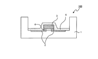
- the binder-type sealant is used for forming the sealing layer 6 of the LED device 100 shown in FIG. 3, for example.
- the wavelength conversion layer 8 that converts the wavelength of light emitted from the LED chip 3 is further provided on the sealing layer 6.
- the sealing layer 6 has a function of sealing the LED element package 1, the metal part 2, the LED chip 3, and the like.
- the sealing layer 6 is formed by applying a binder-type sealant so as to cover the LED element package 1, the metal part 2, the LED chip 3, and the like, and drying and curing it.
- the binder-type sealant is also used for forming the sealing layer 6 of the LED device 100 shown in FIG. 1 or FIG.
- the sealing layer 6 has not only a sealing function for the LED chip 3 and the metal part 2 but also a wavelength conversion function for converting the wavelength of light emitted from the LED chip 3.
- phosphor particles are arranged in advance on a glass substrate 9 for protecting the package 1, the metal part 2, and the LED chip 3; It is formed into a film by applying a binder-type sealant to, drying and curing.
- the phosphor-containing sealant contains polysiloxane, organometallic compound, solvent, and phosphor particles, and if necessary, tabular particles, inorganic fine particles, and the like. .
- the polysiloxane contained in the phosphor-containing sealant can be the same as the polysiloxane contained in the binder-type sealant.
- the amount of polysiloxane contained in the phosphor-containing sealant is preferably such that the amount of polysiloxane in the cured product of the phosphor-containing sealant is 3% by mass or more and 35% by mass or less, and 10% by mass or more and 30% by mass. % Is preferred.
- the polysiloxane functions as a binder in the cured product of the phosphor-containing sealant, if the amount of the binder is less than 3% by mass, a cured film having sufficient coating strength cannot be obtained. On the other hand, when the amount of polysiloxane exceeds 35% by mass, the content of phosphor particles, tabular particles and the like is relatively lowered, and the viscosity of the phosphor-containing encapsulant is likely to be lowered.
- Organometallic compound contained in the phosphor-containing sealant can be the same as the organometallic compound contained in the binder-type sealant.
- the amount of the organometallic compound relative to the amount of polysiloxane can be the same as that of the binder-type sealant described above.
- the solvent contained in the phosphor-containing encapsulant is an aqueous solvent in which water and an organic solvent excellent in water compatibility are combined; or an organic solvent having low water compatibility. Any non-aqueous solvent containing no water may be used. However, when the phosphor particles contained in the phosphor-containing sealant are easily deteriorated by water, a non-aqueous solvent is preferable.
- an aqueous solvent is preferable as described above.
- hydrolysis of polysiloxane is promoted.
- the viscosity of the phosphor-containing sealant increases because the tabular grains described later are swollen. At this time, if impurities are contained in water, swelling of tabular grains and the like may be inhibited. Therefore, it is desirable that the water contained in the phosphor-containing sealant does not contain impurities.
- the phosphor particles may be anything that is excited by the wavelength (excitation wavelength) of light emitted from the LED element (LED chip) and emits fluorescence having a wavelength different from the excitation wavelength.
- the phosphor particles that emit yellow fluorescence include YAG (yttrium, aluminum, garnet) phosphors.
- the YAG phosphor can convert blue light (wavelength 420 nm to 485 nm) emitted from the blue LED element into yellow light (wavelength 550 nm to 650 nm).
- the phosphor particles are, for example, 1) mixing a suitable amount of fluoride such as ammonium fluoride as a flux into a mixed raw material having a predetermined composition and pressurizing it to form a molded body; 2) filling the obtained molded body in a crucible; It can be obtained by baking for 2 to 5 hours in the temperature range of 1350 to 1450 ° C. in air.
- fluoride such as ammonium fluoride
- the mixed raw material having a predetermined composition can be obtained by sufficiently mixing oxides of Y, Gd, Ce, Sm, Al, La, Ga, or compounds that easily become oxides at high temperatures in a stoichiometric ratio.
- the mixed raw material having a predetermined composition includes a coprecipitation oxide obtained by coprecipitation with oxalic acid in a solution in which a rare earth element of Y, Gd, Ce, and Sm is dissolved in acid at a stoichiometric ratio, and aluminum oxide. It is obtained by mixing gallium oxide.
- the kind of the phosphor is not limited to the YAG phosphor, and may be another phosphor such as a non-garnet phosphor that does not contain Ce.
- the average particle diameter of the phosphor particles is preferably 1 ⁇ m or more and 50 ⁇ m or less, and more preferably 10 ⁇ m or less.
- the particle diameter of the phosphor particles is too large, a gap generated at the interface between the phosphor particles and polysiloxane becomes large. Thereby, the intensity
- the average particle diameter of the phosphor particles is measured, for example, by a Coulter counter method.
- the amount of phosphor particles contained in the phosphor-containing encapsulant is preferably such that the amount of phosphor particles in the cured film of the phosphor-containing encapsulant is 60 to 95% by mass. Basically, the higher the concentration of the phosphor particles in the cured film of the phosphor-containing sealant, the better. As the concentration of the phosphor particles increases, the binder content decreases, and the distribution of the phosphor particles in the cured film tends to be uniform. Moreover, if the density
- the concentration of the phosphor particles in the cured film of the phosphor-containing sealant is high, the phosphor particles are brought into close contact with each other, so that the strength of the cured film of the phosphor-containing sealant is increased. Furthermore, when the concentration of the phosphor particles in the cured film is high, the heat generated by the phosphor particles is easily dissipated.
- the concentration of the phosphor particles in the cured film of the phosphor-containing encapsulant is too high (greater than 95% by mass), the binder (polysiloxane) content ratio is extremely reduced, and the phosphor particles There are cases where they cannot be bound together.
- the concentration of the phosphor particles in the cured film is determined from the amount of phosphor particles added to the phosphor-containing sealant.
- the phosphor-containing sealant may contain tabular grains together with the phosphor grains.
- grains When flat particle
- the tabular grains form a card house in the phosphor-containing sealant. Therefore, when tabular grains are included, the viscosity of the phosphor-containing sealant is greatly increased.
- a typical example of the tabular particles contained in the phosphor-containing sealant is layered clay mineral fine particles.
- the main component of the layered clay mineral fine particles is a layered silicate mineral, preferably a swellable clay mineral having a mica structure, a kaolinite structure, a smectite structure, etc., and a swellable clay mineral having a smectite structure rich in swelling properties. More preferred. Since the layered clay mineral fine particles have a flat plate shape, the film strength of the cured film of the phosphor-containing sealant tends to increase.
- the amount of tabular grains is preferably such that the amount of tabular grains in the cured film of the phosphor-containing encapsulant is 0.5% by mass or more and 20% by mass or less, and 0.5% by mass or more and 10% by mass or less. Is more preferred. If the content of tabular grains in the cured film is less than 0.5% by mass, the effect of adding tabular grains cannot be sufficiently obtained. On the other hand, when the content of the layered silicate mineral exceeds 20% by mass, the strength of the phosphor-containing sealant is lowered.
- the surface of the layered clay mineral fine particles may be modified (surface treatment) with an ammonium salt or the like in consideration of compatibility with the solvent.
- the phosphor-containing sealant may contain inorganic fine particles.
- the inorganic fine particles enter the gaps between the phosphor particles, and the strength of the cured film of the phosphor-containing sealant is increased. Further, when the inorganic fine particles are porous, the solvent enters the porous voids, and the viscosity of the phosphor-containing sealing agent is effectively increased.
- the specific surface area of the inorganic fine particles is preferably 200 m 2 / g or more.
- inorganic fine particles include fine oxide particles such as zirconium oxide, silicon oxide, titanium oxide, and zinc oxide, and fine fluoride particles such as magnesium fluoride.
- the average particle size of the inorganic fine particles contained in the phosphor-containing sealant is preferably 1 nm or more and 50 ⁇ m or less, more preferably 1 nm to 10 ⁇ m, and further preferably 1 nm to 100 nm in consideration of the respective effects described above.
- the average particle diameter of the inorganic fine particles is measured, for example, by a Coulter counter method.
- the amount of the inorganic fine particles contained in the phosphor-containing sealant is preferably such that the amount of the inorganic fine particles is 0.5% by mass or more and 50% by mass or less in the cured product of the phosphor-containing sealant. ⁇ 40% by weight.
- the amount of the inorganic fine particles is less than 0.5% by mass, the gap between the phosphor particles cannot be filled with the inorganic fine particles, and the above-described thickening effect and film strength improving effect cannot be obtained.
- the amount of the inorganic fine particles is less than 0.5% by weight, the phosphor particle component is relatively increased, so that the handling property at the time of applying the phosphor-containing sealant is lowered. Therefore, it becomes difficult to form a layer with uniform chromaticity.
- the amount of the inorganic fine particles exceeds 50% by mass, the inorganic fine particles excessively scatter the excitation light of the LED element, so that the light extraction efficiency of the LED device is lowered.
- the surface of the inorganic fine particles may be treated with a silane coupling agent or a titanium coupling agent.
- the surface treatment increases the compatibility between the inorganic fine particles and the polysiloxane.
- the pH of the phosphor-containing sealant is preferably 1 to 4. When the pH is less than 1 or exceeds 4, polysiloxane or an organometallic compound tends to react during storage, and precipitation or the like may occur.
- a pH adjuster such as nitric acid may be added as necessary.
- the viscosity of the phosphor-containing sealant is preferably 10 to 1000 cP, more preferably 12 to 800 cP, and still more preferably 20 to 600 cP.
- the viscosity of the phosphor-containing sealant is preferably 10 to 1000 cP, more preferably 12 to 800 cP, and still more preferably 20 to 600 cP.
- the viscosity of the phosphor-containing sealant is too low, the phosphor-containing sealant flows at the time of application, and the sealing layer cannot be applied to the target region.
- the viscosity of the phosphor-containing encapsulant is too high, it may be difficult to apply the phosphor-containing encapsulant, and the embeddability of the LED element may be poor.
- the viscosity is adjusted by the amount of the inorganic fine particles and the amount of tabular particles.
- the phosphor-containing sealant contains phosphor particles, polysiloxane, organometallic compound, and if necessary, inorganic fine particles, tabular particles, etc. Prepare by mixing.
- each component is not particularly limited.
- water is used as a part of the solvent, 1) premix the tabular grains (which have been subjected to lipophilic surface treatment) in a dispersion solvent other than water, and then A mode in which polysiloxane, organometallic compound, phosphor particles, inorganic fine particles, and water are added to and mixed with, and 2) Preliminary mixing of tabular particles (lipophilic surface-treated) and water, Thereafter, it is preferable to stir the polysiloxane, the organometallic compound, the phosphor particles, and the inorganic oxide together with a dispersion solvent other than water.
- the viscosity tends to increase.
- the stirring of the mixed liquid can be performed by, for example, a stirring mill, a blade kneading stirring device, a thin film swirling disperser, or the like. By adjusting the stirring conditions, it is possible to suppress sedimentation of the phosphor particles in the phosphor-containing sealant.
- the phosphor-containing sealant is used for forming the sealing layer 6 of the LED device 100 shown in FIG. 1 or FIG.
- the sealing layer 6 has not only a sealing function for the LED chip 3, the metal part 2, etc., but also a wavelength conversion function for converting the wavelength of light emitted from the LED chip 3.
- the sealing layer 6 is coated with a phosphor-containing sealing agent so as to cover the LED element package 1, the metal part 2, the glass substrate 9 protecting the LED chip 3, etc., and then dried and cured. A film is formed.
- LED device The LED device of the present invention includes the following three modes. All of the LED devices are excellent in resistance to sulfide gas, and cracks and peeling do not easily occur even when used for a long time.
- An LED device having an LED element and a sealing layer for sealing the LED element, wherein the sealing layer is made of a cured film of the above-described sealing agent for LED device.
- LED element and An LED device having a light-transmitting layer covering the light-transmitting layer and a wavelength conversion layer disposed so as to be in contact with the light-transmitting layer, the light-transmitting layer including polysiloxane, metal oxide fine particles, and a solvent LED device comprising cured film of composition for light transmissive layer (3) LED element, primer layer covering the LED element, light transmissive layer disposed in contact with the primer layer, and disposed on the light transmissive layer LED device having a wavelength conversion layer
- a 1st LED device has an LED element and the sealing layer which coat
- the said sealing layer consists of a cured film of the sealing agent for LED devices mentioned above.
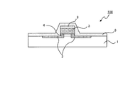
- the first LED device may have a structure having an LED element including a package (LED substrate) 1 and an LED chip 3 and a sealing layer 6 covering the LED element as shown in FIGS. 1 to 3, for example.
- a wavelength conversion layer 8 for converting the light emitted from the LED chip 3 into light of another specific wavelength may be included.
- the LED element includes a package (LED substrate) 1, a metal part 2, an LED chip 3 arranged in the package 1, a metal part 2, and an LED.
- a protruding electrode 4 for connecting the chip 3 is provided.
- a glass substrate 9 that covers the LED chip 3 may be included.
- Package 1 is, for example, liquid crystal polymer or ceramic, but the material is not particularly limited as long as it has insulation and heat resistance. Further, the shape thereof is not particularly limited, and may be a flat plate shape as shown in FIG. 1 or a shape having a recess as shown in FIGS.
- the LED chip 3 is, for example, a blue LED.
- blue LED configurations include an n-GaN compound semiconductor layer (cladding layer), an InGaN compound semiconductor layer (light emitting layer), and a p-GaN compound semiconductor layer (cladding layer) stacked on the LED substrate 1. ) And a transparent electrode layer.
- the LED chip 3 has a surface of, for example, 200 to 300 ⁇ m ⁇ 200 to 300 ⁇ m, and the height of the LED chip 3 is about 50 to 200 ⁇ m.
- the metal part 2 is a wiring made of a metal such as silver, and may function as a reflecting plate that reflects light emitted from the LED chip 3.
- the metal part 2 may be connected to the LED chip via the protruding electrode 4 or may be connected via a metal wire.
- a mode in which the metal part 2 and the LED chip 3 are connected via the protruding electrode 4 is referred to as a flip chip type, and a mode in which the metal part 2 and the LED chip 3 are connected through a metal wire is referred to as a wire bonding type.
- the glass substrate 9 covering the light emitting surface of the LED chip 3 is disposed for the purpose of protecting the LED chip.
- the thickness of the glass substrate is usually 200 to 2000 ⁇ m.
- the sealing layer 6 is made of a cured film of the above-described sealing agent for LED devices.
- the sealing layer 6 may include (i) phosphor particles, and (ii) may not include phosphor particles.
- the wavelength conversion site for the sealing layer 6 to convert the wavelength of the emitted light of the LED chip Serves as a function.
- the sealing layer containing the phosphor particles is referred to as a “wavelength conversion type sealing layer”.
- the thickness of the wavelength conversion type sealing layer 6 is not particularly limited because it is set according to the amount of phosphor required by the LED device. However, the thickness of the wavelength conversion type sealing layer 6 is preferably 150 ⁇ m or less, and more preferably 100 ⁇ m or less. When the thickness of the wavelength conversion type sealing layer 6 exceeds 150 ⁇ m, the concentration of the phosphor particles in the wavelength conversion type sealing layer 6 becomes excessively low, the phosphor particles are not uniformly dispersed, and the film strength is low. There is.
- the lower limit of the thickness of the wavelength conversion type sealing layer 6 is not particularly limited, but is usually 15 ⁇ m or more, preferably 20 ⁇ m or more.
- the phosphor particles and the inorganic fine particles contained in the wavelength conversion type sealing layer 6 have a smaller particle size than the thickness of the wavelength conversion type sealing layer 6.
- the thickness of the wavelength conversion type sealing layer 6 means the maximum thickness of the layer disposed on the upper surface of the glass substrate 9 or the upper surface of the light emitting surface of the LED chip 3 (see FIGS. 1 and 2). Moreover, the thickness of the wavelength conversion type sealing layer 6 disposed on the glass substrate 9 or the upper surface of the light emitting surface of the LED chip 3 means the maximum thickness. The layer thickness is measured using a laser holo gauge.
- the wavelength conversion type sealing layer 6 is formed by applying the above phosphor-containing sealant (one liquid type) and applying the above binder type sealant and phosphor dispersion, respectively. Thus, it is roughly classified into a method (two-component type).
- the phosphor-containing sealant is applied so as to cover at least the metal part (metal wiring) 2, the side surface of the LED chip 3 arranged in the package 1, and the glass substrate 9 of the LED element.
- the application means is not particularly limited, and examples thereof include blade application, spin coat application, dispenser application, and spray application.
- spray coating is preferable because a thin coating film can be easily formed, and thus a thin ceramic layer can be easily formed.
- the polysiloxane and the organometallic compound are dried and cured by heating the coating film to 100 ° C. or higher, preferably 150 to 300 ° C. If the heating temperature is less than 100 ° C., water and the like generated during the dehydration condensation of the silane compound cannot be sufficiently removed, and the light resistance of the coating film may be lowered.
- the wavelength conversion type sealing layer 6 may be covered with a protective layer or the like.
- the protective layer is formed by a spray device or a dispenser device.
- the wavelength conversion type sealing layer 6 is formed in a two-pack type, 1) a step of applying a phosphor dispersion liquid and arranging phosphor particles so as to cover the above-described LED element, and 2) a phosphor dispersion The above-described binder-type sealant is applied and cured so as to cover the LED element to which the liquid is applied. According to this method, the wavelength conversion type sealing layer 6 including the phosphor-containing particles therein is formed.
- a phosphor dispersion liquid is applied and phosphor particles are arranged so as to cover the LED element described above.
- the phosphor dispersion liquid may be a dispersion liquid in which phosphor particles and tabular particles are dispersed in a solvent.
- the phosphor dispersion liquid may further contain inorganic fine particles. That is, it can be the same as the phosphor-containing sealant except that the polysiloxane and the organometallic compound are not included.
- the solvent of the phosphor dispersion liquid preferably contains alcohols.
- the alcohol may be a monohydric alcohol such as methanol, ethanol, propanol, or butanol, or a dihydric or higher polyhydric alcohol. Two or more alcohols may be combined. When a divalent or higher alcohol is contained, the viscosity of the phosphor dispersion liquid is likely to increase, and sedimentation of the phosphor particles as a dispersoid is suppressed.
- the dihydric or higher polyhydric alcohol is not particularly limited; examples thereof include ethylene glycol, propylene glycol, diethylene glycol, glycerin, 1,3-butanediol, 1,4-butanediol, and preferably ethylene glycol Propylene glycol, 1,3-butanediol, 1,4-butanediol, and the like.
- the phosphor dispersion is prepared in the same manner as the phosphor-containing sealant described above. For example, it can be obtained by mixing phosphor particles in a solvent and then mixing tabular particles or inorganic fine particles.
- the above-mentioned one-component phosphor-containing sealant contains a solvent, phosphor particles, polysiloxane, organometallic compound, inorganic fine particles, tabular particles, etc., and causes a chemical reaction over time after the liquid is prepared.
- the viscosity may increase with time.
- a phosphor dispersion liquid that does not contain a binder-type sealant such as polysiloxane or an organometallic compound does not cause such a chemical reaction and becomes a stable liquid with a long pot life.
- the phosphor dispersion liquid is applied so as to cover at least the metal part (metal wiring) 2, the side surface of the LED chip 3 arranged in the package 1, and the glass substrate 9 of the LED element.
- the application means is not particularly limited, and examples thereof include blade application, spin coat application, dispenser application, and spray application. In particular, spray coating is preferable because a thin coating film can be easily formed. After application of the phosphor dispersion liquid, the coating film is dried as necessary.
- the binder-type sealant described above is applied so as to cover the LED element to which the phosphor dispersion liquid has been applied.
- the method for applying the binder sealant is not particularly limited, and may be blade coating, spin coating coating, dispenser coating, spray coating, or the like. In particular, spray coating is preferable because a thin coating film can be easily formed.
- the polysiloxane and the organometallic compound are dried and cured by heating the coating film to 100 ° C. or higher, preferably 150 to 300 ° C. If the heating temperature is less than 100 ° C., the organic components and the like generated during the dehydration condensation of the silane compound cannot be sufficiently removed, and the light resistance of the coating film may be lowered.
- the phosphor dispersion liquid and the binder type sealing agent may be alternately and repeatedly applied to the LED element. Further, after the wavelength conversion type sealing layer 6 is formed, the wavelength conversion type sealing layer 6 may be covered with a protective layer or the like.
- the sealing layer 6 contains a metal element derived from an organometallic compound, the refractive index of the sealing layer 6 tends to fall between the refractive index of the LED chip surface and the refractive index of the wavelength conversion layer 8. . As a result, the interface reflection caused by the difference in refractive index of each layer is reduced, and the light extraction efficiency is increased as compared with the case where only the wavelength conversion layer 8 is provided.
- the thickness of the sealing layer 6 is not particularly limited, but is preferably 4 ⁇ m or less, and more preferably 2 ⁇ m or less. Since the sealing layer 6 does not contain particles having a size of 10 ⁇ m or more, it is preferably set to the above value or less from the viewpoint of crack resistance. On the other hand, the lower limit of the thickness of the sealing layer 6 is not particularly limited, but is usually 0.3 ⁇ m or more, preferably 1 ⁇ m or more.
- the particle size of the inorganic fine particles contained in the sealing layer 6 is smaller than the thickness of the sealing layer 6.
- the thickness of the sealing layer 6 means the maximum thickness of the layer disposed on the upper surface of the LED chip 3.
- the layer thickness is measured using a laser holo gauge.
- the sealing layer 6 is formed by applying the binder-type sealant described above.
- the binder-type sealant is used for the metal part (metal wiring) 2 of the LED element, the LED chip 3 disposed in the package 1, and the protruding electrode 4 that connects the metal part 2 and the LED chip 3. Then, it is applied so as to cover the light emitting surface of the LED chip 3.
- the application means is not particularly limited, and may be blade coating, spin coating coating, dispenser coating, spray coating, or the like. In particular, spray coating is preferable because a thin coating film can be easily formed.
- the polysiloxane and the organometallic compound are dried and cured by heating the coating film to 100 ° C. or higher, preferably 150 to 300 ° C. If the heating temperature is less than 100 ° C., water and the like generated during the dehydration condensation of the silane compound cannot be sufficiently removed, and the light resistance of the coating film may be lowered.
- the wavelength conversion layer 8 is a layer for converting the emission wavelength of the LED chip, and is laminated on the above-described sealing layer 6 (sealing layer not including phosphor particles).
- the wavelength conversion layer 8 is a layer in which phosphor particles are dispersed in a transparent resin.
- the phosphor particles contained in the wavelength conversion layer 8 may be the same as the phosphor particles contained in the aforementioned LED device sealant (phosphor-containing sealant).
- the transparent resin contained in the wavelength conversion layer 8 can be a transparent thermosetting resin. Specific examples include silicone resins and epoxy resins, with silicone resins being particularly preferred.
- the film thickness of the wavelength conversion layer 8 is not particularly limited because it is set according to the amount of phosphor required by the LED device.
- the thickness of the wavelength conversion layer 8 is usually preferably 25 ⁇ m to 5 mm, more preferably 1 to 3 mm. If the thickness of the wavelength conversion layer 8 exceeds the upper limit value, the concentration of the phosphor particles in the wavelength conversion layer 8 is usually excessively low, so that the phosphor particles may not be uniformly dispersed.
- the concentration of the phosphor particles in the wavelength conversion layer is preferably 5 to 15% by mass, more preferably 9 to 11% by mass.
- the wavelength conversion layer 8 is formed by dispersing phosphor particles in a liquid transparent resin (thermosetting resin) and applying the dispersion onto the sealing layer 6 using an injection device such as a dispenser. Thereafter, this dispersion may be cured by heating.
- a liquid transparent resin thermosetting resin
- the second LED device has an LED element, a translucent layer 7, and a wavelength conversion layer 8.
- the light transmissive layer 7 is a cured film of the composition for light transmissive layer containing polysiloxane, metal oxide fine particles, and a solvent.
- the LED element includes a package (LED substrate) 1, a metal part 2, an LED chip 3 arranged in the package 1, a metal part 2, and an LED.
- Metal wiring or protruding electrodes 4 for connecting the chip 3 are provided.
- a glass substrate (not shown) for covering the LED chip 3 may be included.
- the LED elements in the second LED device may be the same as the LED elements in the first LED device.
- the translucent layer 7 is a cured film of a composition for translucent layer containing polysiloxane, metal oxide fine particles, and a solvent, and covers the LED element described above. Covering the LED element means covering at least the light emitting surface of the LED chip 3 and the metal part 2. For example, as shown in FIG. 4, the LED package 1 and the metal wiring 4 may not be completely covered.
- the metal part 2 By covering the metal part 2 with the light-transmitting layer 7, corrosion of the metal part 2 over time can be prevented, and the light extraction efficiency can be maintained well over a long period of time. Moreover, when the light-transmitting layer 7 is provided on the light emitting surface of the LED chip 3, the light from the LED chip 3 is scattered, and the light extraction efficiency is increased.
- the thickness of the light transmitting layer 7 is preferably 0.5 to 10 ⁇ m, more preferably 0.8 to 5 ⁇ m, and further preferably 1 to 2 ⁇ m. When the thickness of the light transmitting layer is 0.5 ⁇ m or less, it is difficult to form a film with a uniform thickness, and when the thickness of the light transmitting layer is 10 ⁇ m or more, the strength of the light transmitting layer 7 may not be sufficient.
- the thickness of the translucent layer 7 means the maximum thickness of the layer arrange
- composition for a light-transmitting layer for forming a light-transmitting layer contains polysiloxane, metal oxide fine particles, and a solvent, and includes a metal alkoxide, a metal chelate, and various additives as necessary.
- the polysiloxane may be a polymer of a monomer containing a tetrafunctional silane compound.
- the monomer may include not only a tetrafunctional silane compound but also a trifunctional silane compound or a bifunctional silane compound.
- the amount of the tetrafunctional silane compound contained in the monomer is preferably 20 to 80% by mass, more preferably 30 to 70% by mass. If the content of the tetrafunctional silane compound is excessive, the degree of crosslinking of the polysiloxane increases, and shrinkage occurs during film formation, and cracks are likely to occur.
- the amount of the tetrafunctional silane compound is excessively small, a large amount of organic groups derived from the trifunctional silane compound or the bifunctional silane compound will remain in the light transmitting layer 7. As a result, the wettability of the composition for forming the wavelength conversion layer 8 is lowered, and the adhesion between the light transmitting layer 7 and the wavelength conversion layer 8 is lowered.
- the monomer preferably includes a tetrafunctional silane compound and a trifunctional silane compound, and particularly preferably includes a tetrafunctional silane compound and a trifunctional monomethylsilane compound.
- the polysiloxane is preferably a polymer of monomers composed of a tetrafunctional silane compound and a trifunctional monomethylsilane compound. These polymerization ratios are not particularly limited, but the polymerization molar ratio is preferably 3: 7 to 7: 3, more preferably 4: 6 to 6: 4.
- the tetrafunctional silane compound contained in the monomer may be the same as the tetrafunctional silane compound contained in the preparation of the polysiloxane of the LED device sealant described above.
- the trifunctional silane compound contained in the monomer may be the trifunctional monomethylsilane contained in the preparation of the polysiloxane of the aforementioned LED device sealant, or the following compound.
- trifunctional silane compounds other than trifunctional monomethylsilane include trimethoxysilane, triethoxysilane, tripropoxysilane, tripentyloxysilane, triphenyloxysilane, dimethoxymonoethoxysilane, diethoxymonomethoxysilane, dipropoxy Monomethoxysilane, dipropoxymonoethoxysilane, dipentyloxylmonomethoxysilane, dipentyloxymonoethoxysilane, dipentyloxymonopropoxysilane, diphenyloxylmonomethoxysilane, diphenyloxymonoethoxysilane, diphenyloxymonopropoxysilane, methoxyethoxypropoxysilane , Monopropoxydimethoxysilane, monopropoxydiethoxysilane, monobutoxydimethoxysilane, monopentyloxy Monohydrosilane compounds such as ethoxysilane and
- each R 4 independently represents an alkyl group or a phenyl group, preferably an alkyl group having 1 to 5 carbon atoms or a phenyl group.
- R 5 each independently represents a hydrogen atom or an alkyl group.
- bifunctional silane compound examples include dimethoxysilane, diethoxysilane, dipropoxysilane, dipentyloxysilane, diphenyloxysilane, methoxyethoxysilane, methoxypropoxysilane, methoxypentyloxysilane, methoxyphenyloxysilane, and ethoxypropoxysilane.
- the mass average molecular weight of the polysiloxane is preferably 1000 to 3000, more preferably 1200 to 2700, and still more preferably 1500 to 2000.
- the mass average molecular weight is less than 1000, the viscosity is low, and liquid repellency or the like is likely to occur during the formation of the light transmitting layer.
- the mass average molecular weight exceeds 3000, the viscosity becomes high, and it may be difficult to form a uniform film, or the embedding property of the LED element may be poor.
- the mass average molecular weight is a value (polystyrene conversion) measured by gel permeation chromatography.
- the polysiloxane is obtained by hydrolyzing and condensing a monomer containing a tetrafunctional silane compound, a trifunctional silane compound, or the like in the presence of an acid catalyst, water, or an organic solvent; It can be the same as the preparation method of polysiloxane contained in
- the composition for a light-transmitting layer contains metal oxide fine particles.
- a cured film of the composition for light transmissive layer that is, when metal oxide fine particles are contained in the light transmissive layer 7, irregularities are generated on the surface of the light transmissive layer 7, and anchors are formed between the light transmissive layer 7 and the wavelength conversion layer 8. The effect appears. Further, due to the unevenness, the wettability of the composition for forming the wavelength conversion layer 8 is improved, and the adhesion between the translucent layer 7 and the wavelength conversion layer 8 is increased.
- the metal oxide fine particles when included in the translucent layer 7, the metal oxide fine particles scatter the light from the LED chip 3, so that the light extraction efficiency from the LED device 100 is increased. Furthermore, the film strength of the translucent layer 7 is also improved. Moreover, when the metal oxide fine particles are contained in the composition for the light transmissive layer, the stress generated in the film at the time of polycondensation or drying of the polysiloxane is relieved, and the light transmissive layer 7 is hardly cracked.
- the type of metal oxide fine particles is not particularly limited, but is preferably particles having a high refractive index.
- the refractive index of the light transmitting layer 7 is increased.
- the refractive index changes gradually from the LED element side in the order of the LED element, the translucent layer 7, the wavelength conversion layer 8, and the atmosphere; since reflection at the interface of each layer is suppressed, Increases light extraction efficiency.
- the metal oxide fine particles are preferably oxide fine particles containing at least one metal selected from the group consisting of zirconium, titanium, tin, cerium, tantalum, niobium and zinc. These may contain only 1 type and may contain 2 or more types. These metal oxide fine particles have a high refractive index. As a result, the refractive index of the translucent layer 7 tends to fall between the refractive index of the surface of the LED chip 3 and the refractive index of the wavelength conversion layer 8. Among these, the metal oxide fine particles are preferably zirconium oxide fine particles because the refractive index is particularly high and the effect of improving the refractive index of the translucent layer 7 is high.
- the average primary particle size of the metal oxide fine particles is preferably 5 to 100 nm, more preferably 5 to 80 nm, and further preferably 5 to 50 nm.
- the average primary particle size of the metal oxide fine particles is measured by a Coulter counter method.
- the metal oxide fine particles are preferably porous, and the specific surface area is preferably 200 m 2 / g or more.
- the solvent enters the porous voids, and the viscosity of the composition for light transmissive layer is effectively increased.
- the viscosity of the light-transmitting layer composition is not simply determined by the amount of the metal oxide fine particles, but also varies depending on the ratio of the metal oxide fine particles and the solvent, the amount of other components, and the like.
- the amount of the metal oxide fine particles in the light transmissive layer composition is preferably 10 to 60% by weight, more preferably 15 to 45% by weight, based on the total solid content of the light transmissive layer composition. More preferably, it is 20 to 30% by mass. If the amount of the metal oxide fine particles is too small, the above-described anchor effect, light scattering effect, refractive index lowering effect and the like cannot be obtained sufficiently. On the other hand, if the amount is too large, the amount of polysiloxane is relatively reduced, and the strength of the light-transmitting layer may be reduced.
- the surface of the metal oxide fine particles may be treated with a silane coupling agent or a titanium coupling agent. By the surface treatment, the compatibility between the metal oxide fine particles and the polysiloxane is increased.
- the solvent contained in the light-transmitting layer composition is not particularly limited.
- the solvent may be an aqueous solvent combining water and an organic solvent excellent in water compatibility; or an organic solvent having low water compatibility and not containing water.
- Examples of the organic solvent having excellent compatibility with water include alcohols such as methanol, ethanol, propanol, and butanol.
- the solvent is preferably an aqueous solvent, and the solvent preferably contains water.
- the amount of water is preferably 3 to 15% by mass, more preferably 5 to 10% by mass, with respect to the total amount of the light-transmitting layer composition. Further, the amount is preferably 10 to 120 parts by weight, more preferably 80 to 100 parts by weight with respect to 100 parts by weight of the above-mentioned polysiloxane. If the amount of water is too small, the polysiloxane is not sufficiently hydrolyzed during the formation of the light transmissive layer, and the moisture and heat resistance of the light transmissive layer is not sufficiently increased. On the other hand, when the amount of water is excessive, hydrolysis may occur during storage of the composition for light transmissive layer, and gelation or the like may occur.
- the solvent preferably contains an organic solvent having a boiling point of 150 ° C. or higher, such as ethylene glycol or propylene glycol.
- an organic solvent having a boiling point of 150 ° C. or higher is contained, the storage stability of the light-transmitting layer composition is increased, and the light-transmitting layer composition can be stably applied from a coating apparatus.
- the boiling point of the solvent is 250 ° C. or lower, the drying property of the composition for light transmissive layer is enhanced.
- the light-transmitting layer composition may contain an organometallic compound comprising a metal alkoxide or metal chelate containing a metal element other than Si element.
- the organometallic compound forms a metalloxane bond with the above-described polysiloxane, a hydroxyl group present on the surface of the LED element or the wavelength conversion layer, and the like at the time of forming the light transmitting layer.
- the metalloxane bond is very strong. Therefore, when an organometallic compound is contained, the adhesiveness of the translucent layer 7 and LED element, and the translucent layer 7 and the wavelength conversion layer 8 increases.
- a part of the organometallic compound forms a nano-sized cluster composed of a metalloxane bond in the light transmitting layer 7. Due to the photocatalytic effect of this cluster, it is possible to oxidize a highly corrosive sulfide gas or the like existing in the vicinity of the LED device 100 and change it to a less corrosive sulfur dioxide gas or the like.
- the metal element contained in the organometallic compound is preferably a group 4 or group 13 metal element other than the Si element.
- the organometallic compound may be the same as the organometallic compound contained in the aforementioned LED device sealant.
- the light-transmitting layer composition is prepared by adding polysiloxane, metal oxide fine particles, organometallic compounds, various additives, and the like to a solvent. It is manufactured by stirring this mixed solution.
- the order of addition of each component is not particularly limited.
- the mixed liquid is stirred by, for example, a stirring mill, a blade kneading stirring device, a thin film swirling disperser, or the like. By adjusting the stirring conditions, settling of the metal oxide fine particles is suppressed.
- the translucent layer 7 is formed by arranging the above-described translucent layer composition on at least the metal portion (metal wiring) 2 and the package 1 of the above-described LED element.
- the LED chip 3 is applied and formed so as to cover the light emitting surface.
- the application means is not particularly limited, and may be blade coating, spin coating coating, dispenser coating, spray coating, or the like. In particular, spray coating is preferable because it easily forms a thin coating film and easily forms a thin light-transmitting layer.
- the polysiloxane is dried and cured by heating the coating film to 100 ° C. or higher, preferably 150 to 300 ° C. If the heating temperature is less than 100 ° C., the organic components and the like generated during dehydration condensation cannot be sufficiently removed, and the light resistance and the like of the translucent layer 7 may be reduced.
- the wavelength conversion layer 8 is a layer that converts light with a specific wavelength emitted from the LED chip 3 into light with another specific wavelength.
- the wavelength conversion layer 8 may be a layer in which phosphor particles are dispersed in a transparent resin.
- the wavelength conversion layer 8 can be the same as the wavelength conversion layer of the first LED device described above.
- the third LED device has an LED element, a primer layer 5, a translucent layer 7, and a wavelength conversion layer 8.
- the LED element includes a package (LED substrate) 1, a metal part 2, an LED chip 3 arranged in the package 1, a metal part 2, and an LED.
- Metal wiring or protruding electrodes 4 for connecting the chip 3 are provided.
- a glass substrate (not shown) for covering the LED chip 3 may be included.
- the LED element in the third LED device may be the same as the LED element in the first LED device.
- the primer layer 5 covers the LED element, and a light transmitting layer 7 described later is laminated on the primer layer 5. Covering the LED element means to cover at least the light emitting surface of the LED chip 3 and the metal part 2 as shown in FIG. 6, and the package 1 and the wiring 4 may not be completely covered. . However, it is preferable that the primer layer 5 covers a part of the package 1.
- the primer layer 5 is a cured film of a composition for a primer layer containing an organometallic monomer having a reactive functional group and a solvent; the primer layer 5 has a function of improving the binding property between the LED element and the light transmitting layer 7. Fulfill.
- the metal of the organometallic monomer contained in the primer layer 5 forms a metalloxane bond with the hydroxyl group present on the surface of the LED chip 3 or the metal part 2 and the polysiloxane contained in the translucent layer, respectively. .
- the LED chip 3 and the metal part 2 and the translucent layer 7 are firmly bonded via the primer layer 5, and even if a load due to temperature occurs, it is difficult to peel between them.
- the thickness of the primer layer 5 is not particularly limited, but is preferably thinner than the wavelength emitted from the LED chip 3 (for example, blue light (420 nm to 485 nm)), more preferably 10 to 120 nm, still more preferably 20 to 90 nm. .
- the thickness of the primer layer 5 means the maximum thickness of the primer layer 5 disposed on the LED chip 3.
- the thickness of the primer layer 5 is measured by a laser holo gauge.
- the primer layer 5 preferably contains 10 at% to 35 at%, and preferably 20 at% to 30 at%, of the metal element derived from the organometallic monomer on the surface thereof with respect to all elements present on the surface.
- the amount of the metal element is 10 at% or more, the metal element sufficiently contributes to the above-described metalloxane bond, and the binding property between the LED element and the translucent layer 7 is increased.
- the amount of metal element is measured by X-ray electron spectroscopy or the like.
- the primer layer 5 is formed by applying and drying a primer layer composition containing an organometallic monomer and a solvent on the LED element.
- This composition for primer layers contains an organometallic monomer and a solvent, and if necessary, various additives such as a stabilizer.
- Organometallic monomer is a monomer having a metal element and a reactive functional group, and is a compound that forms a metalloxane bond by hydrolysis and polycondensation reaction.
- the reactive functional group refers to a group that is hydrolyzed with water to generate a hydroxyl group rich in reactivity.
- the organometallic monomer is preferably a metal alkoxide or metal chelate (organometallic compound) represented by the following general formula (VI).
- M represents a metal element.
- M represents the valence of M and represents 2-4.
- n represents the number of X groups and is an integer of 2 or more and 4 or less.
- m ⁇ n.
- metal element represented by M silane, titanium, or zirconium is preferable, and zirconium is particularly preferable.
- a film made of a metalloxane polymer of zirconium does not have an absorption wavelength in a light emission wavelength region (particularly blue light (wavelength 420 nm to 485 nm)) of a general LED chip. That is, since the primer layer 5 containing a zirconium-based metal element transmits light emitted from the LED element without absorbing it, the light extraction performance is improved.
- X represents a reactive functional group.
- the number of reactive functional groups (n) of the organometallic monomer is 2 to 4 as described above, and preferably 3 or 4.
- the metal in the organometallic monomer forms a dense metalloxane bond with the hydroxyl group present on the surface of the LED chip 3 or the metal part 2 and the polysiloxane contained in the translucent layer. It is easy to form and the binding property between the LED element and the translucent layer 7 is increased.
- Examples of the reactive functional group represented by X include a lower alkoxy group having 1 to 5 carbon atoms, an acetoxy group, a butanoxime group, and a chloro group.
- the plurality of Xs may all be the same reactive functional group or may be a combination of a plurality of types.
- a lower alkoxy group having 1 to 5 carbon atoms is preferable because a component liberated after the reaction is neutral, and a methoxy group or an ethoxy group is more preferable.
- These are highly reactive and can be easily removed because the liberated components (methanol or ethanol) are light boiling.
- Y represents a monovalent organic group.
- the monovalent organic group include groups known as monovalent organic groups of so-called silane coupling agents.
- These may have atoms or atomic groups such as O, N, and S as a linking group.
- a methyl group is preferable from the viewpoint that the light resistance and heat resistance of the primer layer can be improved.
- the organic group may have a substituent.
- substituents include halogen atoms such as F, Cl, Br, and I; vinyl group, methacryloxy group, acryloxy group, styryl group, mercapto group, epoxy group, epoxycyclohexyl group, glycidoxy group, amino group, cyano group, Examples thereof include organic functional groups such as nitro group, sulfonic acid group, carboxy group, hydroxy group, acyl group, alkoxy group, imino group, and phenyl group.
- organometallic monomer may be the same compounds as the specific examples of the organometallic compound contained in the aforementioned LED device sealant.
- the solvent included in the primer layer composition may be any solvent that can dissolve or uniformly disperse the organometallic monomer.
- examples include monohydric alcohols such as methanol, ethanol, propanol and n-butanol; alkyl carboxylic acid esters such as methyl-3-methoxypropionate and ethyl-3-ethoxypropionate; ethylene glycol, diethylene glycol, propylene Polyhydric alcohols such as glycol, glycerin, trimethylolpropane, hexanetriol; ethylene glycol monomethyl ether, ethylene glycol monoethyl ether, ethylene glycol monopropyl ether, ethylene glycol monobutyl ether, diethylene glycol monomethyl ether, diethylene glycol monoethyl ether, diethylene glycol monopropyl Ether, diethylene glycol monobutyl ether, propylene glycol monome Monoethers of polyhydric alcohols such as ether, propylene glycol and al
- the amount of the solvent is preferably 200 to 1500 parts by mass, more preferably 300 to 1200 parts by mass, and further preferably 500 to 900 parts by mass with respect to 100 parts by mass of the organometallic monomer.
- the amount of the solvent is excessive, it takes time to dry the primer layer composition when it is applied and dried.
- the amount of the solvent is too small, the viscosity of the primer layer composition increases, and the primer layer composition may not be applied uniformly.
- the primer layer composition is obtained by adding the above-mentioned organometallic monomer, various additives and the like to a solvent to obtain a mixed solution, which is stirred.
- the order of addition of each component is not particularly limited.
- the mixed liquid is stirred using, for example, a stirring mill, a blade kneading stirring device, a thin-film swirling disperser, or the like.
- the primer layer is composed of the above-described primer layer composition and at least the metal portion (metal wiring) 2 of the above-described LED element and the LED chip disposed in the package 1. 3 is applied so as to cover the light emitting surface 3.
- the application means is not particularly limited, and may be blade coating, spin coating coating, dispenser coating, spray coating, or the like. In particular, spray coating is preferable because a thin primer layer 5 can be easily formed.
- the application amount of the primer layer composition is preferably such that the amount of the organometallic monomer is 0.3 to 3.0 ⁇ l per 1 mm 2 , more preferably 0.5 to 1.0 ⁇ l.
- the primer layer can be formed uniformly on the light emitting surface of the metal part 2 or the LED chip 3.
- the solvent is dried. Drying may be performed at room temperature, but is preferably performed at 60 to 90 ° C, more preferably 70 to 80 ° C. If it is the said temperature range, a solvent will dry efficiently.
- the translucent layer 7 is preferably formed on at least the LED chip 3 and the metal part 2 of the LED element via the primer layer 5.
- the translucent layer 7 functions to prevent corrosion of the metal part 2 and to protect the LED chip 3 from external impacts and the like.
- the thickness of the light transmitting layer is preferably 0.5 to 10 ⁇ m, more preferably 0.8 to 5 ⁇ m, and further preferably 1 to 2 ⁇ m.
- the thickness of the light transmissive layer means the maximum thickness of the light transmissive layer disposed on the LED chip 3. The thickness of the layer can be measured using a laser holo gauge.
- the translucent layer 7 is formed by applying and baking a composition for translucent layer containing polysiloxane and a solvent on the primer layer 5 described above.
- the application means is not particularly limited, and examples thereof include blade application, spin coat application, dispenser application, and spray application.
- spray coating is preferable because a thin coating film can be easily formed, and thus a thin light-transmitting layer can be easily formed.
- the polysiloxane is dried and cured by heating the coating film to 100 ° C. or higher, preferably 150 to 300 ° C. If the heating temperature is less than 100 ° C., water and the like generated during dehydration condensation cannot be sufficiently removed, and the light resistance and the like of the translucent layer may be reduced.
- the composition for the light transmissive layer contains polysiloxane and a solvent, and if necessary, contains metal oxide fine particles, organometallic compounds, various additives, and the like.
- the polysiloxane, metal oxide fine particles, organometallic compound, etc. contained in the composition for light transmissive layer are polysiloxane, metal oxide fine particles, organometallic compound, etc. contained in the composition for light transmissive layer of the second LED device. It can be the same. Moreover, the content and preparation method may be the same.
- the wavelength conversion layer 8 is a layer that converts light having a specific wavelength emitted from the LED chip 3 into light having another specific wavelength.
- the wavelength conversion layer 8 may be a layer in which phosphor particles are dispersed in a transparent resin.
- the wavelength conversion layer 8 can be the same as the wavelength conversion layer of the first LED device described above.
- the LED device described above is further provided with other optical components (such as a lens) to form various optical members.
- other optical components such as a lens
- the LED device of the present invention is excellent in sulfur gas resistance, light resistance, heat resistance, and the like, it is suitable for lighting for vehicles, lighting for outdoor use, and the like.
- Example of first LED device ⁇ Evaluation of liquid repellency>
- the LED device sealant was applied to the LED chip with a wet film thickness of 8 ⁇ m by a spray device (TS-MSP-400, manufactured by Taitec Solutions). At this time, whether or not liquid droplets were formed on the light emitting surface of the LED chip, the silver reflector, and the resin package was evaluated according to the following criteria.
- ⁇ ⁇ Drops are not generated on the light emitting surface and the silver reflector, but droplets with a contact angle of less than 40 ° are generated on the resin package: ⁇ -Droplets with a contact angle of 40 ° or more are generated on the light emitting surface, the silver reflector, and the resin package.
- the center line average roughness Ra value of the coating film is less than 200 nm:
- the center line average roughness Ra value of the coating film is 200 nm or more and less than 250 nm: ⁇
- the center line average roughness Ra value of the coating film is 250 nm or more: x
- the ratio of the total luminous flux to the initial ratio (total luminous flux after exposure to sulfurized gas / total luminous flux before exposure to sulfurized gas x 100) is 96% or more:
- the ratio of the total luminous flux to the initial ratio (total luminous flux value after exposure to sulfurized gas / total luminous flux value before sulfurized gas exposure ⁇ 100) is 92% or more and less than 96%:
- ⁇ -The total luminous flux to initial ratio (total luminous flux value after exposure to sulfurized gas / total luminous flux value before sulfurized gas exposure x 100) is less than 92%:
- ⁇ Crack resistance evaluation> The appearance of the sealing layer of each LED device thus produced was observed with a scanning electron microscope SEM (VE7800, manufactured by Keyence) at a magnification of 1000 times. About each, the crack tolerance evaluation was performed on the following reference
- ⁇ Pot life evaluation> The LED device sealant was allowed to stand at room temperature for 3 weeks. Thereafter, precipitates were evaluated with a dynamic light scattering particle size measuring instrument (Desla nano S, manufactured by Beckman Coulter, Inc.), and pot life was evaluated according to the following criteria. -There is no generation of fine particles in the LED device sealant: ⁇ -Fine particles or gelled products having a particle size of 100 nm to 500 nm are generated in the LED device sealant: ⁇ -Particles or gelled products having a particle size exceeding 500 nm are generated in the LED device sealant: X
- the average transmittance decrease from 300 nm to 500 nm of the treated sample is less than 1.0%: -The average transmittance reduction of the treated sample from 300 nm to 500 nm is 1.0% or more and less than 1.5%: ⁇ -The average transmittance decrease from 300 nm to 500 nm of the treated sample is 1.5% or more: x
- ⁇ Heat and heat resistance evaluation> The produced LED device was allowed to stand at a temperature of 60 ° C. and a relative humidity of 90% RH for 1000 hours. For each LED device, the total luminous flux was measured before and after the test, and the moisture and heat resistance was evaluated according to the following criteria.
- the ratio of the total luminous flux to the initial ratio is 96% or more: ⁇ -Total luminous flux to initial ratio (total luminous flux value after test / total luminous flux value before test x 100) is 92% or more and less than 96%: ⁇ -Total luminous flux to initial ratio (total luminous flux value after test / total luminous flux value before test x 100) is less than 92%: x
- the light extraction property of the produced LED device was measured using a spectral radiance meter (CS-1000, manufactured by Konica Minolta Sensing). As a measurement condition, an electric current of 10 mA was applied, and evaluation was performed with a relative value when the total luminous flux value of an LED device having no sealing layer was 1.0.
- the relative value is 1.1 or more: The relative value is 1.03 to 1.09: ⁇ The relative value is 0.98 to 1.02: ⁇ The relative value is 0.97 or less: ⁇
- the obtained fired product was pulverized, washed, separated, and dried to obtain yellow phosphor particles having an average particle diameter of about 10 ⁇ m.
- the emission wavelength of excitation light with a wavelength of 465 nm was measured, it had a peak wavelength at a wavelength of approximately 570 nm.
- LED devices 1-1 to 1-60 A method for manufacturing LED devices (LED devices 1-1 to 1-60) having the configuration shown in FIG. 1 will be described below.
- Example 1 ⁇ Production of LED device 1-1> 47.3 g of methyltrimethoxysilane, 13.1 g of tetramethoxysilane, 40.0 g of methanol, and 40.0 g of acetone were mixed and stirred. Thereto, 54.6 g of water and 4.7 ⁇ L of 60% nitric acid were added, and the mixture was further stirred for 3 hours. Thereafter, it was aged at 26 ° C. for 2 days.
- the obtained composition is diluted with methanol so that the polysiloxane solid content value becomes 10%, and the polyfunctionality of trifunctional monomethylsilane compound: tetrafunctional silane compound is 8: 2, and the pH is 4.
- a solution was obtained.
- 0.57 g of acetylacetone (manufactured by Kanto Chemical Co., Inc.) as a stabilizer and 3.0C of ZC580 (manufactured by Matsumoto Fine Chemical Co., Ltd.) as a Zr chelate are added to 20.0 g of the polysiloxane solution and stirred.
- a chelate-containing sealant for LED device (binder-type sealant) was obtained.
- phosphor particles prepared by the above-described method 0.05 g of MK-100 (synthetic mica, manufactured by Co-op Chemical), RX300 (average particle diameter of primary particles 7 nm, specific surface area 300 m 2 / g, Nippon Aerosil Co., Ltd.) (0.05 g) and propylene glycol (1.5 g) were mixed to prepare a phosphor dispersion (two-component type).
- the prepared phosphor dispersion liquid was spray-coated on an LED element (LED chip) having the configuration shown in FIG. 1 and dried at 50 ° C. for 1 hour to place phosphor particles on the LED element.
- one blue LED chip (cuboid: 200 ⁇ m ⁇ 300 ⁇ m ⁇ 100 ⁇ m) is flip-chip mounted in the center of a flat package, and a glass substrate (200 ⁇ m ⁇ 300 ⁇ m ⁇ 500 ⁇ m) is arranged on the LED chip.
- An LED chip mounting package was obtained.
- the above-mentioned encapsulant for LED device (binder type encapsulant) containing the Zr group rate was spray-coated on the phosphor particles arranged by the aforementioned method. Thereafter, the LED device 1-1 having a 20 ⁇ m-thick sealing layer (wavelength conversion type sealing layer) containing phosphor particles is obtained by firing at 150 ° C. for 1 hour and providing the phosphor-containing sealing layer 6. It was.
- Example 2 ⁇ Production of LED device 1-2> The LED device 1-1 and the LED device 1-1 were prepared except that the liquid agitation time of the mixed solution of methyltrimethoxysilane, tetramethoxysilane, methanol, acetone, water, and nitric acid when preparing the sealant for the LED device was 6 hours. Similarly, LED device 1-2 was obtained.
- LED device 1-3 was obtained in the same manner as LED device 1-1 except that the amount of methyltrimethoxysilane added was 41.3 g and the amount of tetramethoxysilane added was 19.8 g.
- Example 4 ⁇ Production of LED device 1-4> The LED device 1-3 and the LED device 1-3 were prepared except that the stirring time of the mixed solution of methyltrimethoxysilane, tetramethoxysilane, methanol, acetone, water, and nitric acid was 6 hours when preparing the sealant for the LED device. Similarly, LED device 1-4 was obtained.
- Example 5 Provide of LED device 1-5> An LED device 1-5 was obtained in the same manner as the LED device 1 except that the addition amount of methyltrimethoxysilane was 29.4 g and the addition amount of tetramethoxysilane was 32.9 g.
- Example 6 Provide of LED device 1-6> Except that the stirring time of the mixed solution of methyltrimethoxysilane, tetramethoxysilane, methanol, acetone, water, and nitric acid when preparing the sealant for the LED device was 4.5 hours, the LED device 1- LED device 1-6 was obtained in the same manner as in Example 5.
- Example 7 ⁇ Production of LED device 1-7> LED device 1-5, except that the stirring time of the mixed solution of methyltrimethoxysilane, tetramethoxysilane, methanol, acetone, water, and nitric acid when preparing the sealant for LED device was 6 hours Similarly, LED device 1-7 was obtained.
- Example 8 ⁇ Production of LED device 1-8> An LED device 1-8 was obtained in the same manner as the LED device 1-1 except that the addition amount of methyltrimethoxysilane was 17.7 g and the addition amount of tetramethoxysilane was 46.1 g.
- Example 9 Provide of LED device 1-9> LED device 1-8, except that the stirring time of the mixed solution of methyltrimethoxysilane, tetramethoxysilane, methanol, acetone, water, and nitric acid when preparing the sealant for LED device was 6 hours Similarly, LED device 1-9 was obtained.
- Example 10 ⁇ Production of LED device 1-10> An LED device 1-10 was obtained in the same manner as the LED device 1-1 except that the addition amount of methyltrimethoxysilane was 11.7 g and the addition amount of tetramethoxysilane was 52.8 g.
- Example 11 ⁇ Production of LED device 1-11> LED device 1-10, except that the stirring time of the mixed solution of methyltrimethoxysilane, tetramethoxysilane, methanol, acetone, water, and nitric acid when preparing the sealant for LED device was 6 hours Similarly, LED device 1-11 was obtained.
- Comparative Example 1 ⁇ Production of LED device 1-12> An LED device 1-12 was obtained in the same manner as the LED device 1-1 except that the amount of methyltrimethoxysilane added was 29.4 g and that 26.0 g of dimethoxydimethylsilane was added instead of tetramethoxysilane.
- LED device 1-13 Comparative Example 2 ⁇ Production of LED device 1-13> LED device 1-12, except that the stirring time of the mixed solution of methyltrimethoxysilane, dimethoxydimethylsilane, methanol, acetone, water, and nitric acid was 6 hours when preparing the sealant for LED device Similarly, LED device 1-13 was obtained.
- Comparative Example 3 ⁇ Production of LED device 1-14> Except that the stirring time of the mixed solution of methyltrimethoxysilane, dimethoxydimethylsilane, methanol, acetone, water and nitric acid when preparing the sealant for the LED device was 0.5 hour, the LED device 1- LED device 1-14 was obtained in the same manner as in Example 12.
- Comparative Example 4 ⁇ Production of LED device 1-15> Same as LED device 1-12, except that the stirring time of the mixed solution of methyltrimethoxysilane, dimethoxydimethylsilane, methanol, acetone, water and nitric acid when preparing the sealant for LED device was 8 hours LED device 1-15 was obtained.
- LED device 1-16 was obtained in the same manner as LED device 1-1 except that tetramethoxysilane was not added and 59.0 g of methyltrimethoxysilane was used when preparing the polysiloxane solution.
- the LED device is the same as the LED device 1-16 except that the stirring time of the mixed solution of methyltrimethoxysilane, methanol, acetone, water, and nitric acid when preparing the sealant for the LED device is set to 6 hours. 1-17 was obtained.
- Comparative Example 7 ⁇ Production of LED device 1-18> Similar to the LED device 1-16 except that the stirring time of the mixed solution of methyltrimethoxysilane, methanol, acetone, water and nitric acid when preparing the sealant for the LED device was 0.5 hour, LED device 1-18 was obtained.
- Comparative Example 8 ⁇ Production of LED device 1-19>
- the LED device is the same as the LED device 1-16 except that the stirring time of the mixed solution of methyltrimethoxysilane, methanol, acetone, water and nitric acid when preparing the sealant for the LED device is 8 hours. 1-19 was obtained.
- Comparative Example 9 ⁇ Production of LED device 1-20> Except that the stirring time of the mixed solution of methyltrimethoxysilane, tetramethoxysilane, methanol, acetone, water, and nitric acid when preparing the sealant for the LED device was 0.5 hour, the LED device 1- As in Example 1, LED device 1-20 was obtained.
- Comparative Example 10 ⁇ Production of LED device 1-21>
- the LED device 1-1 and the LED device 1-1 were prepared except that the stirring time of the mixed solution of methyltrimethoxysilane, tetramethoxysilane, methanol, acetone, water, and nitric acid was 8 hours when preparing the sealant for the LED device. Similarly, LED device 1-21 was obtained.
- Comparative Example 11 ⁇ Production of LED device 1-22> LED device 1-3 except that the stirring time of the mixed solution of methyltrimethoxysilane, tetramethoxysilane, methanol, acetone, water, and nitric acid when preparing the sealant for LED device was 0.5 hour. LED device 1-22 was obtained in the same manner as above.
- Comparative Example 12 ⁇ Production of LED device 1-23> Same as LED device 1-3, except that the stirring time of the mixed solution of methyltrimethoxysilane, tetramethoxysilane, methanol, acetone, water, and nitric acid when preparing the sealant for LED device was 8 hours LED device 1-23 was obtained.
- Comparative Example 13 ⁇ Production of LED device 1-24> Except that the stirring time of the mixed solution of methyltrimethoxysilane, tetramethoxysilane, methanol, acetone, water, and nitric acid when preparing the sealant for the LED device was 0.5 hour, the LED device 1- LED device 1-24 was obtained in the same manner as in Example 5.
- Comparative Example 14 ⁇ Production of LED device 1-25> LED device 1-5, except that the stirring time of the mixed solution of methyltrimethoxysilane, tetramethoxysilane, methanol, acetone, water, and nitric acid when preparing the sealant for LED device was 8 hours. Similarly, LED device 1-25 was obtained.
- Comparative Example 15 ⁇ Production of LED device 1-26> Except that the stirring time of the mixed solution of methyltrimethoxysilane, tetramethoxysilane, methanol, acetone, water, and nitric acid when preparing the sealant for the LED device was 0.5 hour, the LED device 1- LED device 1-26 was obtained in the same manner as in Example 8.
- Comparative Example 16 ⁇ Production of LED device 1-27> Except that the stirring time of the mixed solution of methyltrimethoxysilane, tetramethoxysilane, methanol, acetone, water, and nitric acid when preparing the sealant for the LED device was 0.5 hour, the LED device 1- LED device 1-27 was obtained in the same manner as in Example 8.
- Comparative Example 17 ⁇ Production of LED device 1-28> LED device 1-10, except that the stirring time of the mixed solution of methyltrimethoxysilane, tetramethoxysilane, methanol, acetone, water, and nitric acid when preparing the sealant for LED device was 0.5 hour LED device 1-28 was obtained in the same manner as above.
- Comparative Example 18 ⁇ Production of LED device 1-29> Same as LED device 1-10, except that the stirring time of the mixed solution of methyltrimethoxysilane, tetramethoxysilane, methanol, acetone, water, and nitric acid when preparing the sealant for LED device was 8 hours LED device 1-29 was obtained.
- Comparative Example 19 ⁇ Production of LED device 1-30> An LED device 1-30 was obtained in the same manner as the LED device 1-1 except that methyltrimethoxysilane was not added and 65.9 g of tetramethoxysilane was added when preparing the LED device sealant.
- the LED device 1-30 is the same as the LED device 1-30, except that the stirring time of the mixed solution of tetramethoxysilane, methanol, acetone, water and nitric acid is 6 hours when preparing the sealant for the LED device. 31 was obtained.
- Comparative Example 21 ⁇ Production of LED device 1-32> In the same manner as the LED device 1-30, except that the stirring time of the mixed solution of tetramethoxysilane, methanol, acetone, water, and nitric acid was set to 0.5 hour when preparing the sealant for the LED device. Device 1-32 was obtained.
- the LED device 1 is the same as the LED device 1-30 except that the stirring time of the mixed solution of tetramethoxysilane, methanol, acetone, water, and nitric acid is 8 hours when preparing the sealant for the LED device. -33 was obtained.
- LED device 1-34 was obtained in the same manner as LED device 1-6 except that the amount of Zr chelate ZC580 (manufactured by Matsumoto Fine Chemical Co., Ltd.) was changed to 0.14 g.
- LED device 1-35 was obtained in the same manner as LED device 1-6 except that the amount of Zr chelate ZC580 (manufactured by Matsumoto Fine Chemical Co., Ltd.) was 2.85 g.
- LED device 1-36 was obtained in the same manner as LED device 1-6 except that 0.1 g of Ti alkoxide TA25 (manufactured by Matsumoto Fine Chemical Co.) was added instead of Zr chelate ZC580 (manufactured by Matsumoto Fine Chemical Co., Ltd.).
- LED device 1-37 was obtained in the same manner as LED device 1-6 except that 0.4 g of Ti alkoxide TA25 (manufactured by Matsumoto Fine Chemical Co.) was added instead of Zr chelate ZC580 (manufactured by Matsumoto Fine Chemical Co., Ltd.).
- LED device 1-38 was obtained in the same manner as LED device 1-6 except that 2.0 g of Ti alkoxide TA25 (manufactured by Matsumoto Fine Chemical Co.) was added instead of Zr chelate ZC580 (manufactured by Matsumoto Fine Chemical Co., Ltd.).
- LED device 1-39 was obtained in the same manner as LED device 1-6, except that 0.1 g of Al alkoxide ALR15GB (manufactured by Koyo Chemical Co., Ltd.) was added instead of Zr chelate ZC580 (manufactured by Matsumoto Fine Chemical Co., Ltd.).
- Example 18 ⁇ Production of LED device 1-40> An LED device 1-40 was obtained in the same manner as the LED device 1-6 except that 0.4 g of Al alkoxide ALR15GB (manufactured by Koyo Chemical Co., Ltd.) was added instead of Zr chelate ZC580 (manufactured by Matsumoto Fine Chemical Co., Ltd.).
- LED device 1-41 was obtained in the same manner as LED device 1-6, except that 2.0 g of Al alkoxide ALR15GB (manufactured by Kojundo Chemical Co., Ltd.) was added instead of Zr chelate ZC580 (manufactured by Matsumoto Fine Chemical Co., Ltd.).
- LED device 1-42 was obtained in the same manner as LED device 1-6, except that Zr chelate ZC580 (manufactured by Matsumoto Fine Chemical Co., Ltd.) was not added.
- LED device 1-43 was obtained in the same manner as LED device 1-6, except that the amount of Zr chelate ZC580 (manufactured by Matsumoto Fine Chemical Co., Ltd.) was changed to 4.28 g.
- LED device 1-44 was obtained in the same manner as LED device 1-6 except that 3.0 g of Ti alkoxide TA25 (manufactured by Matsumoto Fine Chemical Co.) was added instead of Zr chelate ZC580 (manufactured by Matsumoto Fine Chemical Co., Ltd.).
- LED device 1-45 was obtained in the same manner as LED device 1-6, except that 3.0 g of Al alkoxide ALR15GB (manufactured by Koyo Chemical Co., Ltd.) was added instead of Zr chelate ZC580 (manufactured by Matsumoto Fine Chemical Co., Ltd.).
- Example 20 ⁇ Production of LED device 1-46> An LED device 1-46 was obtained in the same manner as the LED device 1-6 except that 0.2 g of pure water was added to the LED device sealant.
- Example 21 Provide of LED device 1-47> An LED device 1-47 was obtained in the same manner as the LED device 1-6 except that 1.2 g of pure water was added to the LED device sealant.
- Example 22 ⁇ Production of LED device 1-48> An LED device 1-48 was obtained in the same manner as the LED device 1-6 except that 2.4 g of pure water was added to the sealant for the LED device.
- LED device 1 is the same as LED device 1-47 except that nitric acid is added to the sealant for the LED device until the pH measured with a pH meter (YK-21PH, manufactured by Sato Corporation) becomes 0.8. -49 was obtained.
- LED device 1 is the same as LED device 1-47 except that nitric acid is added to the LED device sealant until the pH measured by a pH meter (YK-21PH, manufactured by Sato Corporation) reaches 1.0. -50 was obtained.
- LED device 1 is the same as LED device 1-47 except that nitric acid is added to the sealant for the LED device until the pH measured with a pH meter (YK-21PH, manufactured by Sato Corporation) is 4.0. -51 was obtained.
- LED device 1 is the same as LED device 1-47 except that nitric acid is added to the sealant for the LED device until the pH measured by a pH meter (YK-21PH, manufactured by Sato Corporation) is 5.0. -52 was obtained.
- LED device 1-53 was obtained in the same manner as LED device 1-49, except that 2.0 g of a slurry (SZR-M, manufactured by Sakai Chemical Co., Ltd.) in which ZrO 2 fine particles were dispersed was added to the LED device sealant.
- SZR-M a slurry in which ZrO 2 fine particles were dispersed
- Example 28 ⁇ Production of LED device 1-54> An LED device 1-54 was obtained in the same manner as the LED device 1-50, except that 2.0 g of a slurry (SZR-M, manufactured by Sakai Chemical Co., Ltd.) in which ZrO 2 fine particles were dispersed was added to the sealant for the LED device. .
- SZR-M a slurry in which ZrO 2 fine particles were dispersed
- Example 29 ⁇ Production of LED device 1-55> An LED device 1-55 was obtained in the same manner as the LED device 1-51 except that 2.0 g of a slurry (SZR-M, manufactured by Sakai Chemical Co., Ltd.) in which ZrO 2 fine particles were dispersed was added to the sealant for the LED device. .
- SZR-M a slurry in which ZrO 2 fine particles were dispersed
- Example 30 ⁇ Production of LED device 1-56> An LED device 1-56 was obtained in the same manner as the LED device 1-52, except that 2.0 g of a slurry (SZR-M, manufactured by Sakai Chemical Co., Ltd.) in which ZrO 2 fine particles were dispersed was added to the sealant for the LED device. .
- SZR-M a slurry in which ZrO 2 fine particles were dispersed
- LED device 1-57 was obtained in the same manner as LED device 1-49, except that the firing temperature of the LED device sealant was changed to 80 ° C.
- LED device 1-58 was obtained in the same manner as LED device 1-50, except that the firing temperature of the LED device sealant was 100 ° C.
- LED device 1-59 was obtained in the same manner as LED device 1-53, except that the firing temperature of the LED device sealant was changed to 80 ° C.
- Example 34 Provide of LED device 1-60> An LED device 1-60 was obtained in the same manner as the LED device 1-54 except that the firing temperature of the sealant for the LED device was 100 ° C.
- Table 1 shows the evaluation results of the LED devices of Examples 1 to 11 and Comparative Examples 1 to 22.
- Examples 1 to 11 each including a cured film of polysiloxane having a weight average molecular weight of 1000 to 3000 obtained by polymerizing a trifunctional monomethylsilane compound and a tetrafunctional silane compound, all of them are sealed for LED devices.
- the repellency of the stopping agent was hardly observed, and the smoothness of the film was also good.
- a polysiloxane obtained by polymerizing a trifunctional monomethylsilane compound and a tetrafunctional silane compound is used, if the mass average molecular weight is less than 1000, the coating film shape cannot be maintained at the uneven portion. Liquid repelling occurred in Comparative Examples 9, 11, 13, 15, and 17.
- Comparative Examples 19 to 22 in which only four functional components were used as the silane compound constituting the polysiloxane no liquid repellency was observed, but the film was poor in flexibility and cracks occurred.
- Table 2 shows the evaluation results of the LED devices of Examples 6 and 12 to 19 and Comparative Examples 23 to 26.
- the light extraction efficiency is excellent when a Zr chelate having no absorption in the wavelength region (wavelength 420 nm to 485 nm) of the emitted light of the LED element is used (Examples 6, 12, and 13). It was.
- Table 3 shows the evaluation results of the LED devices of Examples 6 and 20-22.
- Example 20 and 21 containing 10 to 100 parts by mass of water with respect to 100 parts by mass of polysiloxane, the polysiloxane and the organometallic compound undergo a hydrolysis reaction before condensation. Therefore, a denser film was formed and moisture and heat resistance was improved as compared with Example 6 containing no water.
- Example 22 containing more than 100 parts by mass of water with respect to 100 parts by mass of polysiloxane, the hydrolysis reaction with water was fast and the storage stability was lowered.
- Table 4 shows the evaluation results of the LED devices of Examples 23 to 30.
- Table 5 shows the evaluation results of the LED devices of Examples 25, 29, and 31 to 34.
- LED devices 2-1 to 2-60 A method for manufacturing LED devices (LED devices 2-1 to 2-60) having the configuration shown in FIG. 2 will be described below.
- LED element (LED chip) having a package 1 (LED substrate) having a recess having the configuration shown in FIG. 2 was prepared.
- one blue LED chip (in the shape of a rectangular parallelepiped: 200 ⁇ m ⁇ 300 ⁇ m ⁇ 100 ⁇ m) is flip-chip mounted in the center of a housing portion of a circular package (opening diameter 3 mm, bottom surface diameter 2 mm, wall surface angle 60 °)
- a chip mounting package was prepared.
- an LED device sealant similar to the LED devices 1-1 to 1-60 described above is used, and a sealing layer is formed under the same conditions. 2-60 was obtained.
- LED devices 3-1 to 3-60 A method for manufacturing the LED device (LED devices 3-1 to 3-60) having the configuration shown in FIG. 3 will be described below.
- LED element LED chip
- package LED substrate
- recess having the configuration shown in FIG. 3
- one blue LED chip in the shape of a rectangular parallelepiped: 200 ⁇ m ⁇ 300 ⁇ m ⁇ 100 ⁇ m
- one blue LED chip is flip-chip mounted in the center of a housing portion of a circular package (opening diameter 3 mm, bottom surface diameter 2 mm, wall surface angle 60 °)
- a chip mounting package was prepared.
- the same LED device sealant as the LED devices 1-1 to 1-60 described above was used, and a 1.5 ⁇ m thick sealant was used. A stop layer 6 was formed.
- a silicone resin (OE6630, manufactured by Toray Dow Co., Ltd.) in which 10% by mass of the phosphor prepared by the above-described method is dispersed is dropped on the sealing layer 6 with a dispenser, and baked at 150 ° C. for 1 hour. Conversion layer 8 was formed, and LED devices 3-1 to 3-60 were produced. The thickness of the wavelength conversion layer 8 was 2.5 mm.
- the LED devices 2-1 to 2-60 and the LED devices 3-1 to 3-60 were evaluated in the same manner as the LED devices 1-1 to 1-60. As a result, the same results as those of the LED devices 1-1 to 1-60 were obtained.
- Example of second LED device ⁇ Adhesion evaluation> About the LED device produced by the Example and the comparative example, the heat shock test was done using the heat shock tester (TSA-42EL, the product made by Espec). In the test, the LED device was stored at ⁇ 40 ° C. for 30 minutes and then stored at 100 ° C. for 30 minutes as one cycle, and this was repeated. A current was passed through the sample after the test to confirm whether it was lit. Non-lighting occurred due to peeling between the light-transmitting layer and the wavelength conversion layer.
- TSA-42EL the heat shock tester
- the ratio of the total luminous flux to the initial ratio (total luminous flux after exposure to sulfurized gas / total luminous flux before exposure to sulfurized gas x 100) is 96% or more:
- the ratio of the total luminous flux to the initial ratio (total luminous flux value after exposure to sulfurized gas / total luminous flux value before sulfurized gas exposure ⁇ 100) is 92% or more and less than 96%:
- ⁇ -The total luminous flux to initial ratio (total luminous flux value after exposure to sulfurized gas / total luminous flux value before sulfurized gas exposure x 100) is less than 92%:
- ⁇ Crack resistance evaluation> About each LED apparatus, after forming the light transmission layer and before forming the wavelength conversion layer, the appearance was observed with a scanning electron microscope SEM (VE7800, manufactured by Keyence Corporation) at a magnification of 1000 times. About each, the crack tolerance evaluation was performed on the following reference
- the light extraction property of the produced LED device was measured using a spectral radiance meter (CS-1000, manufactured by Konica Minolta Sensing). As a measurement condition, an electric current of 10 mA was applied, and evaluation was performed with a relative value when the total luminous flux value of an LED device having no light-transmitting layer was 1.0.
- the relative value is 1.1 or more: The relative value is 1.03 to 1.09: ⁇ The relative value is 0.98 to 1.02: ⁇ The relative value is 0.97 or less: ⁇
- ⁇ Pot life evaluation> The composition for translucent layer was left still at room temperature for 3 weeks. Thereafter, precipitates were evaluated with a dynamic light scattering particle size measuring instrument (Desla nano S, manufactured by Beckman Coulter, Inc.), and pot life was evaluated according to the following criteria.
- ⁇ Heat and heat resistance evaluation> The produced LED device was allowed to stand at a temperature of 60 ° C. and a relative humidity of 90% RH for 1000 hours. For each LED device, the total luminous flux was measured before and after the test, and the moisture and heat resistance was evaluated according to the following criteria.
- the ratio of the total luminous flux to the initial ratio is 96% or more: ⁇ -Total luminous flux to initial ratio (total luminous flux value after test / total luminous flux value before test x 100) is 92% or more and less than 96%: ⁇ -Total luminous flux to initial ratio (total luminous flux value after test / total luminous flux value before test x 100) is less than 92%: x
- As the phosphor material 7.41 g of Y 2 O 3 , 4.01 g of Gd 2 O 3 , 0.63 g of CeO 2 , and 7.77 g of Al 2 O 3 were sufficiently mixed.
- An appropriate amount of ammonium fluoride was mixed as a flux to this and filled in an aluminum crucible.
- the packing is fired at a temperature range of 1350 to 1450 ° C. for 2 to 5 hours in a reducing atmosphere in which hydrogen-containing nitrogen gas is circulated to obtain a fired product ((Y 0.72 Gd 0.24 ) 3 Al 5 O 12 : Ce 0.04 ).
- the obtained fired product was pulverized, washed, separated, and dried to obtain yellow phosphor particles having an average particle diameter of about 10 ⁇ m.
- the emission wavelength of excitation light with a wavelength of 465 nm was measured, it had a peak wavelength at a wavelength of approximately 570 nm.
- Example 1 Production of LED device 1
- Tetramethoxysilane 36.0 g, methyltrimethoxysilane 10.7 g, dimethoxydimethylsilane 9.48 g, methanol 37.5 g, and acetone 37.5 g were mixed and stirred. Furthermore, 51.1 g of water and 4.4 ⁇ L of 60% nitric acid were added, and the mixture was further stirred for 3 hours. Thereafter, it was aged at 26 ° C. for 2 days.
- the light-transmitting layer composition was spray-coated on the LED element and baked at 150 ° C. for 1 hour to form a light-transmitting layer having a thickness of 1.5 ⁇ m.
- the LED element is an LED chip in which one blue LED chip (in a rectangular parallelepiped shape: 200 ⁇ m ⁇ 300 ⁇ m ⁇ 100 ⁇ m) is flip-chip mounted in the center of a housing portion of a circular package (opening diameter 3 mm, bottom surface diameter 2 mm, wall surface angle 60 °). It was a mounting package.
- a silicone resin (OE6630, manufactured by Toray Dow Co., Ltd.) in which 10% by mass of the phosphor was dispersed was applied on the light-transmitting layer by a dispenser and baked at 150 ° C. for 1 hour to form a wavelength conversion layer.
- the thickness of the wavelength conversion layer was 2.5 mm.
- Example 2 Production of LED device 2
- An LED device 2 was produced in the same manner as in Example 1 except that the ZrO 2 dispersion was changed to 3.0 g of ZnO dispersion (CIK Nanotech Co., Ltd.) in which ZnO fine particles were dispersed.
- the particle diameter of the ZnO fine particles was 52 nm, and the concentration of the ZnO fine particles with respect to the solid content of the light-transmitting layer composition was 45% by mass.
- Example 3 Production of LED device 3
- An LED device 3 was produced in the same manner as in Example 1 except that the ZrO 2 dispersion was changed to 3.0 g of SiO 2 dispersion (CIK Nanotech Co., Ltd.) in which SiO 2 fine particles were dispersed.
- the particle diameter of the SiO 2 fine particles was 30 nm, and the concentration of the SiO 2 fine particles with respect to the solid content of the light-transmitting layer composition was 45% by mass.
- Table 6 shows the evaluation results of the LED devices of Examples 1 to 3 and Comparative Examples 1 and 2.
- the light extraction performance was very good (Example 1). This is because, by adding zirconium oxide having a high refractive index, the refractive index of the light-transmitting layer becomes an intermediate refractive index between the refractive index of the LED chip surface and the refractive index of the wavelength conversion layer, and the reflection generated at the interface of each layer. It was speculated that this could be greatly reduced.
- Example 4 Production of LED device 6
- An LED device 6 was produced in the same manner as in Example 1 except that the ZrO 2 dispersion was added so that the concentration of the ZrO 2 fine particles was 5% by mass with respect to the solid content of the composition for light transmitting layer. .
- Example 5 Production of LED device 7
- An LED device 7 was produced in the same manner as in Example 1 except that the ZrO 2 dispersion was added so that the concentration of the ZrO 2 fine particles was 10% by mass with respect to the solid content of the composition for light transmitting layer. .
- Example 6 Production of LED device 8
- An LED device 8 was produced in the same manner as in Example 1 except that the ZrO 2 dispersion was added so that the concentration of the ZrO 2 fine particles was 30% by mass with respect to the solid content of the composition for light transmissive layer. .
- Example 7 Production of LED device 9
- the LED device 9 was produced in the same manner as the LED device 1 except that the ZrO 2 dispersion was added so that the concentration of the ZrO 2 fine particles was 60% by mass with respect to the solid content of the composition for light transmitting layer. .
- Example 8 Production of LED device 10.
- the LED device 10 was produced in the same manner as the LED device 1 except that the ZrO 2 dispersion was added so that the concentration of the ZrO 2 fine particles was 80% by mass with respect to the solid content of the composition for light transmitting layer. .
- Table 7 shows the evaluation results of the LED devices of Examples 4 to 8 and Comparative Examples 1 and 3.
- the zirconium oxide dispersion is a zirconium oxide dispersion (manufactured by Sakai Chemical Co., Ltd.) in which zirconium oxide (ZrO 2 ) having an average primary particle size of 5 nm is dispersed, and the concentration of zirconium oxide fine particles with respect to the solid content of the composition for the light-transmitting layer
- An LED device 12 was produced in the same manner as in Example 1 except that the amount was 30% by mass.
- Example 10 Production of LED device 13
- Zirconium oxide dispersion, and zirconium oxide having an average primary particle diameter of 10nm zirconium oxide (ZrO 2) are dispersed (ZrO 2) dispersion (TECNAN Co.), relative to the solid content of the light transmitting layer composition of zirconium oxide fine particles
- ZrO 2 zirconium oxide having an average primary particle diameter of 10nm zirconium oxide (ZrO 2) are dispersed (ZrO 2) dispersion (TECNAN Co.), relative to the solid content of the light transmitting layer composition of zirconium oxide fine particles
- An LED device 13 was produced in the same manner as in Example 1 except that the concentration was 30% by mass.
- the zirconium oxide dispersion is a zirconium oxide (ZrO 2 ) dispersion in which zirconium oxide (ZrO 2 ) having an average primary particle size of 20 nm is dispersed (manufactured by CIK Nanotech Co., Ltd.).
- An LED device 14 was produced in the same manner as in Example 1 except that the concentration relative to the minute was 30% by mass.
- Example 12 Production of LED device 15
- Solid zirconium oxide dispersion, and zirconium oxide having an average primary particle diameter 50nm zirconium oxide (ZrO 2) are dispersed (ZrO 2) dispersion liquid (manufactured by CIK Nanotech Co.), light transmitting layer composition of zirconium oxide fine particles
- ZrO 2 dispersed (ZrO 2) dispersion liquid (manufactured by CIK Nanotech Co.), light transmitting layer composition of zirconium oxide fine particles
- An LED device 15 was produced in the same manner as in Example 1 except that the concentration relative to the minute was 30% by mass.
- Example 13 Production of LED device 16
- Solid zirconium oxide dispersion, and zirconium oxide having an average primary particle diameter 200nm zirconium oxide (ZrO 2) are dispersed (ZrO 2) dispersion liquid (manufactured by CIK Nanotech Co.), light transmitting layer composition of zirconium oxide fine particles
- ZrO 2 dispersion liquid manufactured by CIK Nanotech Co.
- the LED device 16 was produced in the same manner as in Example 1 except that the concentration relative to the minute was 30% by mass.
- Table 8 shows the evaluation results of the LED devices of Examples 9 to 13.
- Example 14 Production of LED device 17
- methyltrimethoxysilane, 13.1 g of tetramethoxysilane, 40.0 g of methanol, and 40.0 g of acetone were mixed and stirred. Further, 54.6 g of water and 4.7 ⁇ L of 60% nitric acid were added, and the mixture was further stirred for 3 hours.
- a zirconium oxide (ZrO 2 ) dispersion liquid manufactured by Sakai Chemical Co., Ltd.
- the concentration of zirconium oxide with respect to the solid content of the light-transmitting layer composition was 30% by mass.
- An LED device 17 was produced in the same manner as in Example 1 except that the addition was performed.
- Example 15 Production of LED device 18
- An LED device 18 was produced in the same manner as in Example 14 except that 17.7 g of methyltrimethoxysilane and 46.1 g of tetramethoxysilane were added.
- Example 16 Production of LED device 19
- An LED device 19 was produced in the same manner as in Example 14 except that 29.4 g of methyltrimethoxysilane and 32.9 g of tetramethoxysilane were added.
- Example 17 Production of LED device 20
- An LED device 20 was produced in the same manner as in Example 14 except that 41.3 g of methyltrimethoxysilane and 19.8 g of tetramethoxysilane were added.
- Example 18 Production of LED device 21
- An LED device 21 was produced in the same manner as in Example 14 except that 47.3 g of methyltrimethoxysilane and 13.1 g of tetramethoxysilane were added.
- Example 19 Production of LED device 23
- An LED device 23 was produced in the same manner as in Example 14 except that methyltrimethoxysilane was not added and 65.9 g of tetramethoxysilane was added.
- LED device 24 was fabricated in the same manner as in Example 14 except that 29.4 g of methyltrimethoxysilane and 26.0 g of dimethoxydimethylsilane were added without adding tetramethoxysilane.
- Table 9 shows the evaluation results of the LED devices of Examples 14 to 19 and Comparative Examples 4 and 5.
- Example 20 Production of LED device 25
- 10% by mass of acetylacetone (manufactured by Kanto Chemical Co., Ltd.) as a stabilizer is added to the light transmitting layer composition based on the total amount of the light transmitting layer composition
- ZC-580 (manufactured by Matsumoto Fine Chemical Co., Ltd.) is used as the Zr chelate.
- Example 15 10% by mass of acetylacetone (manufactured by Kanto Chemical Co., Ltd.) as a stabilizer is added to the light transmitting layer composition based on the total amount of the light transmitting layer composition
- ZC-580 manufactured by Matsumoto Fine Chemical Co., Ltd.
- Example 21 Production of LED device 26 Except that Zr chelate was not added, Al alkoxide; ALR15GB (manufactured by High-Purity Chemical Co., Ltd.) was added so that the solid content was 10% by mass with respect to the solid content of the composition for translucent layer. In the same manner as in Example 20, an LED device 26 was produced.
- Example 22 Production of LED device 27 Except that Zr chelate was not added, Ti alkoxide; TA25 (manufactured by Matsumoto Fine Chemical Co., Ltd.) was added so that the solid content was 10% by mass with respect to the solid content of the composition for translucent layer. In the same manner as in Example 20, an LED device 27 was produced.
- Table 10 shows the evaluation results of the LED devices of Examples 15 and 20-22.
- Example 23 Production of LED device 28
- An LED device 28 was produced in the same manner as in Example 20 except that pure water was added in an amount of 3% by mass with respect to the total amount of the polysiloxane solution.
- Example 24 Production of LED device 29
- An LED device 29 was produced in the same manner as in Example 20 except that pure water was added in an amount of 10% by mass with respect to the total amount of the polysiloxane solution.
- Example 25 Production of LED device 30
- An LED device 30 was produced in the same manner as in Example 20 except that pure water was added in an amount of 15% by mass with respect to the total amount of the polysiloxane solution.
- Example 26 Production of LED device 31
- An LED device 31 was produced in the same manner as in Example 20 except that pure water was added in an amount of 25% by mass with respect to the total amount of the polysiloxane solution.
- Table 11 shows the evaluation results of the LED devices of Examples 20 and 23 to 26.
- Example of third LED device ⁇ Adhesion evaluation> About the LED device produced by the Example and the comparative example, the heat shock test was done using the heat shock tester (TSA-42EL, the product made by Espec). In the test, the LED device was stored at ⁇ 40 ° C. for 30 minutes and then stored at 100 ° C. for 30 minutes as one cycle, and this was repeated. A current was passed through the sample after the test to confirm whether it was lit. Non-lighting occurs due to peeling at the interface between the LED chip and the light-transmitting layer or at the interface between the primer layer and the light-transmitting layer.
- TSA-42EL the heat shock tester
- the ratio of the total luminous flux to the initial ratio (total luminous flux after exposure to sulfurized gas / total luminous flux before exposure to sulfurized gas x 100) is 98% or more:
- the ratio of the total luminous flux to the initial ratio (total luminous flux after exposure to sulfurized gas / total luminous flux before exposure to sulfurized gas ⁇ 100) is 96% or more and less than 98%:
- the ratio of the total luminous flux to the initial ratio (total luminous flux value after exposure to sulfurized gas / total luminous flux value before sulfurized gas exposure ⁇ 100) is 92% or more and less than 96%:
- ⁇ -The total luminous flux to initial ratio (total luminous flux value after exposure to sulfurized gas / total luminous flux value before sulfurized gas exposure x 100) is less than 92%:
- ⁇ Crack resistance evaluation> In each example or comparative example, after forming the light-transmitting layer and before forming the wavelength conversion layer, the appearance was observed with a scanning electron microscope SEM (VE7800, manufactured by Keyence) at an enlargement magnification of 1000 times. About each, the crack tolerance evaluation was performed on the following reference
- the primer layer composition was applied on a slide glass and dried at 70 ° C. for 30 minutes. At this time, the thickness of the primer layer after drying was 1 ⁇ m, and the amount of the metal element derived from the organometallic monomer present on the surface of the primer layer was 30 at% with respect to all the elements present on the surface of the primer layer.
- permeability before and behind processing for 150 hours by a metal halide lamp light resistance tester (M6T, Suga Test Instruments Co., Ltd.) for 100 hours was measured, and the light resistance evaluation was performed on the following reference
- the average transmittance decrease from 300 nm to 500 nm of the treated sample is less than 1.0%: -The average transmittance reduction of the treated sample from 300 nm to 500 nm is 1.0% or more and less than 1.5%: ⁇ -The average transmittance decrease from 300 nm to 500 nm of the treated sample is 1.5% or more: x
- ⁇ Pot life evaluation> The composition for translucent layer was left still at room temperature for 3 weeks. Thereafter, precipitates were evaluated with a dynamic light scattering particle size measuring instrument (Desla nano S, manufactured by Beckman Coulter, Inc.), and pot life was evaluated according to the following criteria.
- ⁇ Heat and heat resistance evaluation> The produced LED device was allowed to stand at a temperature of 60 ° C. and a relative humidity of 90% RH for 1000 hours. For each LED device, the total luminous flux was measured before and after the test, and the moisture and heat resistance was evaluated according to the following criteria.
- the ratio of the total luminous flux to the initial ratio is 96% or more: ⁇ -Total luminous flux to initial ratio (total luminous flux value after test / total luminous flux value before test x 100) is 92% or more and less than 96%: ⁇ -Total luminous flux to initial ratio (total luminous flux value after test / total luminous flux value before test x 100) is less than 92%: x
- the light extraction property of the produced LED device was measured using a spectral radiance meter (CS-1000, manufactured by Konica Minolta Sensing). As a measurement condition, a current of 10 mA was applied, and the evaluation was performed with a relative value when the total luminous flux value of an LED device without a primer layer was 1.0.
- the relative value is 1.1 or more: The relative value is 1.03 to 1.09: ⁇ The relative value is 0.98 to 1.02: ⁇ The relative value is 0.97 or less: ⁇
- Example 1 Production of LED device 1
- Al alkoxide ARR15GB (manufactured by Koyo Chemical Co., Ltd.)
- stabilizer acetylacetone
- 2-propanol 4.0 g A primer layer composition was prepared.
- composition for translucent layer Tetramethoxysilane 36.0g, methyltrimethoxysilane 10.7g, dimethoxydimethylsilane 9.48g, methanol 37.5g, and acetone 37.5g were mixed and stirred. Furthermore, 51.1 g of water and 4.4 ⁇ L of 60% nitric acid were added, and the mixture was further stirred for 3 hours. Thereafter, the solution was aged at 26 ° C. for 2 days. The obtained composition was diluted with methanol so that the solid content of the polysiloxane was 10% by mass to obtain a composition for a light-transmitting layer.
- the polysiloxane in the light transmitting layer composition is a compound obtained by polymerizing a quaternary silane compound, a trifunctional silane compound, and a bifunctional silane compound at a polymerization ratio of 6: 2: 2.
- phosphor particles The method for preparing phosphor particles is described below.
- As the phosphor material 7.41 g of Y 2 O 3 , 4.01 g of Gd 2 O 3 , 0.63 g of CeO 2 , and 7.77 g of Al 2 O 3 were sufficiently mixed.
- An appropriate amount of ammonium fluoride was mixed as a flux to this and filled in an aluminum crucible.
- the packing is fired at a temperature range of 1350 to 1450 ° C. for 2 to 5 hours in a reducing atmosphere in which hydrogen-containing nitrogen gas is circulated to obtain a fired product ((Y 0.72 Gd 0.24 ) 3 Al 5 O 12 : Ce 0.04 ).
- the obtained fired product was pulverized, washed, separated, and dried to obtain yellow phosphor particles having an average particle diameter of about 10 ⁇ m.
- the emission wavelength of excitation light with a wavelength of 465 nm was measured, it had a peak wavelength at a wavelength of approximately 570 nm.
- the LED element was prepared and the primer layer composition was spray-coated so that the LED chip of this LED element and a metal part might be coat
- the thickness of the primer layer was 0.1 ⁇ m, and the amount of the metal element derived from the organometallic monomer present on the surface of the primer layer was 30 at% with respect to all the elements present on the surface of the primer layer.
- the LED element was flip-chip mounted with one blue LED chip (cuboid: 200 ⁇ m ⁇ 300 ⁇ m ⁇ 100 ⁇ m) in the center of the accommodating portion of the circular package (opening diameter 3 mm, bottom diameter 2 mm, wall surface angle 60 °). It was set as the LED chip mounting package.
- the composition for light transmissive layer was spray-coated on the primer layer. Then, it baked at 150 degreeC for 1 hour, and formed the translucent layer. The thickness of the light transmissive layer was 1.5 ⁇ m.
- a silicone resin (OE6630, manufactured by Toray Dow Co., Ltd.) in which 10% by mass of phosphor particles were dispersed was applied with a dispenser, and baked at 150 ° C. for 1 hour to form a wavelength conversion layer.
- the thickness of the wavelength conversion layer was 2.5 mm.
- Example 2 Production of LED device 2
- Example 1 except that 0.5 g of Si alkoxide (dimethoxydimethylsilane (D1052, manufactured by Tokyo Chemical Industry Co., Ltd.)) and 4.5 g of 2-propanol were mixed and stirred to prepare a primer layer composition. Then, the LED device 2 was produced.
- Si alkoxide diimethoxydimethylsilane (D1052, manufactured by Tokyo Chemical Industry Co., Ltd.)
- 2-propanol 2-propanol
- Example 3 Production of LED device 3
- Ti chelate titanium acetylacetonate (TC-100, manufactured by Matsumoto Fine Chemical)
- stabilizer acetylacetone
- 2-propanol a primer layer
- An LED device 3 was produced in the same manner as in Example 1 except that the composition was prepared.
- Example 4 Production of LED device 4
- Zr chelate dibutoxyzirconium bisethylacetoacetate (ZC-580, manufactured by Matsumoto Fine Chemical Co.)
- stabilizer acetylacetone
- 2-propanol 2-propanol
- Example 5 Production of LED device 5
- Si alkoxide diimethoxydimethylsilane (D1052, manufactured by Tokyo Chemical Industry Co., Ltd.)
- Ti chelate titanium acetylacetonate (TC-100, manufactured by Matsumoto Fine Chemical Co.)
- stabilizer acetylacetone
- Example 6 Production of LED device 6) 0.25 g of Si alkoxide (dimethoxydimethylsilane (D1052, manufactured by Tokyo Chemical Industry Co., Ltd.)), 0.36 g of Zr chelate (dibutoxyzirconium bisethylacetoacetate (ZC-580, manufactured by Matsumoto Fine Chemical Co.)), and stabilizer LED device 6 was produced in the same manner as in Example 1 except that 0.5 g of (acetylacetone) and 3.89 g of 2-propanol were mixed and stirred to prepare a primer layer composition.
- Si alkoxide diimethoxydimethylsilane (D1052, manufactured by Tokyo Chemical Industry Co., Ltd.)
- Zr chelate dibutoxyzirconium bisethylacetoacetate (ZC-580, manufactured by Matsumoto Fine Chemical Co.
- Table 12 shows the evaluation results of the LED devices of Examples 1 to 6 and Comparative Example 1.
- Ti and Zr do not have an absorption wavelength in the emission wavelength range of the LED chip (particularly blue light (wavelength 420 nm to 485 nm)). Therefore, it is presumed that the light-transmitting layer containing a zirconium-based metal element transmits light emitted from the LED element without absorbing it. In addition, when the primer layer was not formed, the reason why the light extraction performance was poor is presumed to be that the adhesion between the light-transmitting layer and the LED chip or the like was low, and peeling occurred at these interfaces.
- Example 7 Production of LED device 8
- 0.59 g of tetrafunctional Zr alkoxide tetranormal butoxyzirconium (ZA-65, manufactured by Matsumoto Fine Chemical Co.)
- 0.5 g of stabilizer acetylacetone
- 2-propanol a compound that stabilizes 2-propanol
- An LED device 8 was produced in the same manner as in Example 1 except that the primer layer composition was prepared.
- Example 8 Production of LED device 9
- tetrafunctional Zr alkoxide tetranormal butoxyzirconium (ZA-65, manufactured by Matsumoto Fine Chemical)
- trifunctional Zr chelate zirconium tributoxymonoacetylacetonate (ZC-540, manufactured by Matsumoto Fine Chemical)
- 0.56 g, 0.5 g of stabilizer (acetylacetone), and 7.24 g of 2-propanol were mixed and stirred to prepare a primer layer composition.
- LED device 10 Trifunctional Zr chelate (zirconium tributoxy monoacetylacetonate (ZC-540, manufactured by Matsumoto Fine Chemicals)) 1.1 g, stabilizer (acetylacetone) 0.9 g, and 2-propanol 9.1 g were mixed.
- LED device 10 was produced in the same manner as in Example 1 except that the composition for the primer layer was prepared by stirring.
- Table 13 shows the evaluation results of the LED devices of Examples 4 and 7-9.
- Example 10 Production of LED device 11
- 47.3 g of methyltrimethoxysilane, 13.1 g of tetramethoxysilane, 40.0 g of methanol, and 40.0 g of acetone were mixed and stirred. Thereafter, 54.6 g of water and 4.7 ⁇ L of 60% nitric acid were added, and the mixture was further stirred for 3 hours.
- the obtained composition was diluted with methanol so that the solid content concentration of the polysiloxane was 10% by mass to obtain a light-transmitting layer composition.
- the polysiloxane in the composition for light transmissive layer is a compound obtained by polymerizing a trifunctional silane compound and a tetrafunctional silane compound at a ratio of 2: 8.
- An LED device 11 was produced in the same manner as in Example 7 except that the light transmissive layer was formed by forming the light transmissive layer composition.
- Example 11 Production of LED device 12
- An LED device 12 was produced in the same manner as in Example 10 except that the amount of methyltrimethoxysilane was 17.7 g and the amount of tetramethoxysilane was 46.1 g.
- LED device 13 was produced in the same manner as in Example 10, except that the amount of methyltrimethoxysilane was 29.4 g and the amount of tetramethoxysilane was 32.9 g.
- Example 13 Production of LED device 14
- An LED device 14 was produced in the same manner as in Example 10 except that the amount of methyltrimethoxysilane was 41.3 and the amount of tetramethoxysilane was 19.8 g.
- Example 14 Production of LED device 15
- An LED device 15 was produced in the same manner as in Example 10 except that the amount of methyltrimethoxysilane was 47.3 and the amount of tetramethoxysilane was 13.1 g.
- LED device 17 was produced in the same manner as in Example 10 except that tetramethoxysilane was not added, and 29.4 g of methyltrimethoxysilane and 26.0 g of dimethoxydimethylsilane were added.
- Example 15 Production of LED device 18
- An LED device 18 was produced in the same manner as in Example 10 except that methyltrimethoxysilane was not added and 65.9 g of tetramethoxysilane was added.
- Table 14 shows the evaluation results of the LED devices of Examples 10 to 15 and Comparative Examples 2 and 3.
- Example 16 Production of LED device 19
- An LED device 19 was produced in the same manner as in Example 11 except that pure water was added to the light transmissive layer composition in an amount of 3% by mass with respect to the total amount of the light transmissive layer composition.
- Example 17 Production of LED device 20
- the LED device 20 was produced in the same manner as in Example 11 except that pure water was added to the light transmissive layer composition in an amount of 10% by mass with respect to the total amount of the light transmissive layer composition.
- Example 18 Production of LED device 21
- An LED device 21 was produced in the same manner as in Example 11 except that pure water was added to the light transmissive layer composition in an amount of 15% by mass based on the total amount of the light transmissive layer composition.
- Example 19 Production of LED device 22
- An LED device 22 was produced in the same manner as in Example 11 except that pure water was added to the light transmissive layer composition in an amount of 25% by mass based on the total amount of the light transmissive layer composition.
- Table 15 shows the evaluation results of the LED devices of Examples 11 and 16-19.
- Example 20 Production of LED device 23
- a ZrO 2 dispersion manufactured by Sakai Chemical Co., Ltd.
- zirconium oxide (ZrO 2 ) fine particles are dispersed in the composition for light transmissive layer
- the amount of zirconium oxide is 20 with respect to the total solid content of the composition for light transmissive layer.
- An LED device 23 was produced in the same manner as in Example 17 except that an amount of mass% was added.
- Table 16 shows the evaluation results of the LED devices of Examples 17 and 20.
- the sealing film for an LED element formed with the sealing agent for an LED device of the present invention is excellent in resistance to sulfur gas, heat resistance, and light resistance. Therefore, it is useful as a sealing film for LED elements in semiconductor LED devices such as lighting.
Abstract
Description
さらに、特許文献9または10には、金属アルコキシドのゾルゲル反応により、ポリメタロキサンからなる封止材を形成する技術が記載されている。
[1]3官能モノメチルシラン化合物及び4官能シラン化合物を重合した質量平均分子量1000~3000のポリシロキサン100質量部と、4族または13族の金属元素を含む金属アルコキシドまたは金属キレートからなる有機金属化合物5質量部~100質量部と、溶媒とを含む、LED装置用封止剤。
[3]前記有機金属化合物がZrを含む、[1]または[2]に記載のLED装置用封止剤。
[4]前記溶媒として水を含み、水の添加量が、前記ポリシロキサン100質量部に対して、10~120質量部である[1]~[3]のいずれかに記載のLED装置用封止剤。
[6]pHが1~4である、[1]~[5]のいずれかに記載のLED装置用封止剤。
[7]蛍光体粒子をさらに含有する、[1]~[6]のいずれかに記載のLED装置用封止剤。
[8]特定波長の光を出射するLED素子と、[1]~[7]のいずれかに記載のLED装置用封止剤の硬化膜からなる封止層とを有するLED装置。
[9]前記封止層上に、樹脂及び蛍光体粒子を含み、前記LED素子からの特定波長の光を他の特定波長の光に変換する波長変換層をさらに有する[8]に記載のLED装置。
[10]LED素子上に、[1]~[7]のいずれかに記載のLED装置用封止剤を塗布し、100℃以上で硬化させて封止層を形成する工程を含む、LED装置の製造方法。
[11]特定波長の光を出射するLED素子と、前記LED素子を被覆する透光層と、前記透光層と接するように配置され、かつ前記LED素子からの特定波長の光を、他の特定波長の光に変換する波長変換層とを有し、前記透光層が、4官能シラン化合物を含むモノマーを重合したポリシロキサン、金属酸化物微粒子、及び溶媒を含む透光層用組成物の硬化膜からなる、LED装置。
[12]前記金属酸化物微粒子は、ジルコニウム、チタン、スズ、セリウム、タンタル、ニオブ、及び亜鉛の群から選択される1種または2種以上の金属元素の酸化物である、[11]に記載のLED装置。
[13]前記透光層用組成物の固形分に対する、前記金属酸化物微粒子の濃度が10質量%以上60質量%以下である、[11]または[12]に記載のLED装置。
[14]前記金属酸化物微粒子の平均一次粒径が5nm~100nmである、[11]~[13]のいずれかに記載のLED装置。
[16]前記透光層用組成物は、Si元素以外の金属元素を含む金属アルコキシドまたは金属キレートからなる有機金属化合物を含有する、[11]~[15]のいずれかに記載のLED装置。
[17]前記透光層用組成物は、前記溶媒として水を含み、かつ前記水の添加量が、前記透光層用組成物全量に対して3質量%~15質量%である、[11]~[16]のいずれかに記載のLED装置。
[18]前記透光層の厚みが、0.5~10μmである、[11]~[17]のいずれかに記載のLED装置。
[19]特定波長の光を出射するLED素子と、前記LED素子を被覆する透光層と、前記透光層と接するように配置され、かつ前記LED素子からの特定波長の光を他の特定波長の光に変換する波長変換層とを有するLED装置の製造方法であって、4官能シラン化合物を含むモノマーを重合したポリシロキサン、金属酸化物微粒子、及び溶媒を含む透光層用組成物を塗布し、硬化させて透光層を形成する工程を有する、LED装置の製造方法。
[20]特定波長の光を出射するLED素子と、前記LED素子を被覆するプライマー層と、前記プライマー層と接するように配置された透光層と、前記透光層上に配置され、かつ前記LED素子からの特定波長の光を、他の特定波長の光に変換する波長変換層とを有し、反応性官能基を有する有機金属モノマー及び溶媒を含むプライマー層用組成物を、前記LED素子上に塗布・乾燥して前記プライマー層を形成し、4官能シラン化合物を含むモノマーを重合したポリシロキサン及び溶媒を含有する透光層用組成物を、前記プライマー層上に、塗布・焼成して前記透光層を形成したLED装置。
[22]前記有機金属モノマーの前記反応性官能基の数が3または4である、[20]または[21]に記載のLED装置。
[23]前記プライマー層の表面に、前記有機金属モノマー由来の金属元素を、前記表面に存在する元素全体に対して、10at%~35at%含む、[20]~[22]のいずれかに記載のLED装置。
[24]前記ポリシロキサンは、3官能モノメチルシラン化合物及び4官能シラン化合物からなるモノマーの重合体であり、前記3官能モノメチルシラン化合物と、前記4官能シラン化合物との重合モル比率が、3:7~7:3である、[20]~[23]のいずれかに記載のLED装置。
[26]前記透光層用組成物は、金属酸化物微粒子を含有する、[20]~[25]のいずれかに記載のLED装置。
[27]前記透光層の厚みが、0.5~10μmである、[20]~[26]のいずれかに記載のLED装置。
[28]前記波長変換層は、蛍光体粒子が透明樹脂中に分散された層である、[20]~[27]のいずれかに記載のLED装置。
[29]特定波長の光を出射するLED素子と、前記LED素子を被覆するプライマー層と、前記プライマー層と接するように配置された透光層と、前記透光層上に配置され、かつ前記LED素子からの特定波長の光を、他の特定波長の光に変換する波長変換層とを有するLED装置の製造方法であって、反応性官能基を有する有機金属モノマー及び溶媒を含むプライマー層用組成物を、前記LED素子上に塗布・乾燥して前記プライマー層を形成する工程と、4官能シラン化合物を含むモノマーを重合したポリシロキサン及び溶媒を含有する透光層用組成物を、前記プライマー層上に、塗布・焼成して前記透光層を形成する工程とを有するLED装置の製造方法。
本発明のLED装置用封止剤は、LED素子を封止する層の成膜に使用される。本発明のLED装置用封止剤の硬化膜(封止層)は、LED素子との密着性が良好であり、さらに硫化ガスに対する耐性も高い。また当該硬化膜は、厚膜とした場合にも透明性、耐光性、耐熱成に優れ、かつ長期間使用してもクラックを生じることがない。さらにLED装置に当該硬化膜が含まれると、LED装置の光取り出し効率が高まる。
バインダ型封止剤には、ポリシロキサン、有機金属化合物、及び溶媒が含まれ、必要に応じて無機微粒子等が含まれる。
バインダ型封止剤に含まれるポリシロキサンは、3官能モノメチルシラン化合物と、4官能シラン化合物との重合体である。
3官能モノメチルシラン化合物には、下記一般式(I)で表される化合物が含まれる。
CH3Si(OR1)3 …(I)
上記一般式(I)中、R1は、それぞれ独立にアルキル基またはフェニル基を表し、好ましくは炭素数1~5のアルキル基、またはフェニル基を表す。
Si(OR2)4 …(II)
上記一般式(II)中、R2はそれぞれ独立にアルキル基またはフェニル基を表し、好ましくは炭素数1~5のアルキル基、またはフェニル基を表す。
ポリシロキサンは、上記3官能モノメチルシラン化合物及び4官能シラン化合物を、酸触媒、水、有機溶媒の存在下で加水分解し、縮合反応させて調製される。得られるポリシロキサンの質量平均分子量は、反応条件(特に反応時間)等で調整される。
R3-SO3H …(III)
(一般式(III)中、R3は、置換基を有していてもよい炭化水素基である。)
バインダ型封止剤には、4族または13族の金属元素を含む金属アルコキシドまたは金属キレートからなる有機金属化合物が含まれる。前述のように、有機金属化合物中の金属は、ポリシロキサンや、LED素子の各部材表面の水酸基と、メタロキサン結合を形成する。また有機金属化合物の一部は、バインダ型封止剤の硬化膜中で、シロキサン結合からなるナノサイズのクラスタを形成する。
Mm+XnYm-n …(IV)
一般式(IV)中、Mは4族または13族の金属元素を表す。また一般式(IV)中、mはMの価数を表し、3または4を表す。一般式(IV)中、nはX基の数を表し、2以上4以下の整数である。但し、m≧nである。
バインダ型封止剤には、溶媒が含まれる。溶媒は、水と、水との相溶性に優れた有機溶媒を組み合わせた水性溶媒;もしくは、水との相溶性が低い有機溶媒であって、水を含有しない非水性溶媒でありうる。水との相溶性に優れた有機溶媒の例には、例えばメタノール、エタノール、プロパノール、ブタノールなどのアルコール類が含まれる。
バインダ型封止剤には、無機微粒子が含まれてもよい。無機微粒子が含まれると、バインダ型封止剤の粘度が高まり、さらに硬化膜の強度が向上する。さらに、屈折率の高い無機微粒子が含まれると、バインダ型封止剤の硬化膜の光取り出し効率が高まる。
バインダ型封止剤のpHは、1~4であることが好ましい。pHが1未満もしくは4を超えると、ポリシロキサンもしくは有機金属化合物が反応してしまい、保存時に沈殿物等が生じる場合がある。バインダ型封止剤のpH調整のため、必要に応じて、例えば硝酸等、pH調整剤等が含まれてもよい。
バインダ型封止剤は、溶媒に、ポリシロキサンや有機金属化合物、無機微粒子等を混合して調製する。混合液の調製は、任意の方法で行うことができ、例えば、撹拌ミル、ブレード混練撹拌装置、薄膜旋回型分散機などで攪拌する。
バインダ型封止剤は、例えば図3に示されるLED装置100の封止層6の成膜に用いられる。図3に示される構成のLED装置100では、封止層6上にさらに、LEDチップ3から出射する光の波長を変換する波長変換層8を有する。当該LED装置100において、封止層6は、LED素子のパッケージ1、メタル部2、LEDチップ3等を封止する機能を担う。当該封止層6は、LED素子のパッケージ1、メタル部2、LEDチップ3等を被覆するように、バインダ型封止剤を塗布し、これを乾燥・硬化させることで成膜される。
蛍光体含有封止剤には、ポリシロキサン、有機金属化合物、溶媒、及び蛍光体粒子が含まれ、必要に応じて平板状粒子、及び無機微粒子等が含まれる。
蛍光体含有封止剤に含まれるポリシロキサンは、前述のバインダ型封止剤に含まれるポリシロキサンと同様でありうる。蛍光体含有封止剤に含まれるポリシロキサンの量は、蛍光体含有封止剤の硬化物中のポリシロキサン量が3質量%以上35質量%以下となる量が好ましく、10質量%以上30質量%以下となる量が好ましい。
蛍光体含有封止剤に含まれる有機金属化合物は、前述のバインダ型封止剤に含まれる有機金属化合物と同様でありうる。またポリシロキサンの量に対する、有機金属化合物の量も前述のバインダ型封止剤と同様でありうる。
蛍光体含有封止剤に含まれる溶媒は、水と、水との相溶性に優れた有機溶媒を組み合わせた水性溶媒;もしくは、水との相溶性が低い有機溶媒であって、水を含有しない非水性溶媒のいずれであってもよい。ただし、蛍光体含有封止剤に含まれる蛍光体粒子が、水によって劣化しやすい場合には、非水性溶媒が好ましい。
蛍光体粒子は、LED素子(LEDチップ)からの出射光の波長(励起波長)により励起されて、励起波長と異なる波長の蛍光を出射するものであればよい。例えば、LEDチップから青色光が出射する場合、蛍光体含有封止剤の硬化膜に黄色の蛍光を発する蛍光体粒子が含まれると、LED装置から出射する光が白色となる。黄色の蛍光を発する蛍光体粒子の例には、YAG(イットリウム・アルミニウム・ガーネット)蛍光体が挙げられる。YAG蛍光体は、青色LED素子から出射される青色光(波長420nm~485nm)を黄色光(波長550nm~650nm)に変換することができる。
蛍光体含有封止剤には、上記蛍光体粒子と共に、平板状粒子が含まれてもよい。蛍光体含有封止剤に平板状粒子が含まれると、蛍光体含有封止剤の粘度が高まり、該封止剤中での蛍光体粒子の沈降が抑制される。平板状粒子は、蛍光体含有封止剤中においてカードハウスを形成する。そのため、平板状粒子が含まれると、蛍光体含有封止剤の粘度が大幅に高まる。
蛍光体含有封止剤には、無機微粒子が含まれてもよい。無機微粒子が含まれることで、無機微粒子が蛍光体粒子同士の隙間に入り込み、蛍光体含有封止剤の硬化膜の強度が高まる。また無機微粒子が多孔質である場合には、多孔質の空隙部に溶媒が入り込み、蛍光体含有封止剤の粘度が効果的に高まる。無機微粒子の比表面積は200m2/g以上であることが好ましい。
蛍光体含有封止剤のpHは1~4であることが好ましい。pHが1未満もしくは4を超えると、保存中にポリシロキサンや有機金属化合物が反応しやすくなり、沈殿等が生じる場合がある。蛍光体含有封止剤のpH調整のため、必要に応じて、例えば硝酸等、pH調整剤等を添加してもよい。
蛍光体含有封止剤は、溶媒に、蛍光体粒子、ポリシロキサン、有機金属化合物、及び必要に応じて、無機微粒子、平板状粒子等を混合して調製する。
蛍光体含有封止剤は、図1または図2に示されるLED装置100の封止層6の成膜に用いられる。当該LED装置100では、封止層6が、LEDチップ3やメタル部2等の封止機能だけでなく、LEDチップ3から出射する光の波長を変換する波長変換機能も担う。当該封止層6は、LED素子のパッケージ1、メタル部2、LEDチップ3を保護するガラス基板9等を被覆するように、蛍光体含有封止剤を塗布し、これを乾燥・硬化して成膜される。
本発明のLED装置には、以下の3つの態様が含まれる。いずれのLED装置も、硫化ガス耐性に優れ、長期間使用してもクラックや剥離が生じ難い。
(1)LED素子と、これを封止する封止層と、を有するLED装置であって、封止層が前述のLED装置用封止剤の硬化膜からなるLED装置
(2)LED素子と、これを被覆する透光層と、当該透光層に接するように配置された波長変換層と、を有するLED装置であって、透光層がポリシロキサン、金属酸化物微粒子、及び溶媒を含む透光層用組成物の硬化膜からなるLED装置
(3)LED素子と、これを被覆するプライマー層と、当該プライマー層に接するように配置された透光層と、透光層上に配置された波長変換層と、を有するLED装置
第一のLED装置は、LED素子と、これを被覆する封止層とを有し、当該封止層が前述のLED装置用封止剤の硬化膜からなる。第一のLED装置は、例えば、図1~3に示されるように、パッケージ(LED基板)1やLEDチップ3を含むLED素子と、これを覆う封止層6とを有する構造であればよく;例えば図3に示されるように、LEDチップ3からの出射光を、他の特定波長の光に変換するための波長変換層8が含まれてもよい。
LED素子は、図1~3に示されるように、パッケージ(LED基板)1と、メタル部2と、パッケージ1に配置されたLEDチップ3と、メタル部2とLEDチップ3とを接続する突起電極4とを有する。また、図1に示されるように、LEDチップ3を被覆するガラス基板9が含まれてもよい。
封止層6は、前述のLED装置用封止剤の硬化膜からなる。封止層6には、(i)蛍光体粒子が含まれてもよく、(ii)蛍光体粒子が含まれなくてもよい。
封止層6に蛍光体粒子が含まれると、封止層6がLEDチップの出射光を波長変換するための波長変換部位としての機能を果たす。以下、蛍光体粒子が含まれる封止層を「波長変換型封止層」と称する。
波長変換型封止層6を1液型で形成する場合には、前述のLED素子上に、前述の蛍光体含有封止剤を塗布し、これを硬化させる。
波長変換型封止層6を2液型で形成する場合、1)前述のLED素子を被覆するように、蛍光体分散液を塗布して蛍光体粒子を配置する工程と、2)蛍光体分散液を塗布したLED素子を被覆するように、前述のバインダ型封止剤を塗布し、硬化させる工程とを行う。当該方法によれば、内部に蛍光体含有粒子を含む波長変換型封止層6が成膜される。
波長変換型封止層6を2液型で形成する場合、まず、前述のLED素子を被覆するように、蛍光体分散液を塗布して蛍光体粒子を配置する。
蛍光体分散液は、蛍光体粒子と、平板状粒子とを溶媒に分散させた分散液等でありうる。蛍光体分散液には、さらに無機微粒子等が含まれてもよい。つまりポリシロキサン及び有機金属化合物が含まれないこと以外は、蛍光体含有封止剤と同様でありうる。
蛍光体分散液を塗布したLED素子を被覆するように、前述のバインダ型封止剤を塗布する。バインダ型封止剤の塗布方法は特に限定されず、ブレード塗布、スピンコート塗布、ディスペンサー塗布、スプレー塗布などでありうる。特に、スプレー塗布は薄い塗布膜を成膜しやすいために好ましい。
封止層6に、蛍光体粒子が含まれない場合、図3に示されるように、封止層6上にさらに後述の波長変換層8が形成される。LED素子と波長変換層8との間に封止層6が含まれると、LED装置100からの光取り出し効率が高まる。これは以下の理由による。
波長変換層8は、LEDチップの発光波長を変換するための層であり、前述の封止層6(蛍光体粒子を含まない封止層)上に積層される。波長変換層8は、透明樹脂中に蛍光体粒子が分散された層である。波長変換層8に含まれる蛍光体粒子は、前述のLED装置用封止剤(蛍光体含有封止剤)に含まれる蛍光体粒子と同様でありうる。波長変換層8に含まれる透明樹脂は、透明の熱硬化性樹脂でありうる。具体的には、シリコーン樹脂、エポキシ樹脂等が挙げられ、特にシリコーン樹脂が好ましい。
第二のLED装置は、図4及び図5に示されるように、LED素子と、透光層7と、波長変換層8とを有する。透光層7は、ポリシロキサン、金属酸化物微粒子、及び溶媒を含む透光層用組成物の硬化膜である。
LED素子は、図4及び5に示されるように、パッケージ(LED基板)1と、メタル部2と、パッケージ1に配置されたLEDチップ3と、メタル部2とLEDチップ3とを接続する金属配線もしくは突起電極4とを有する。また、LEDチップ3を被覆するガラス基板(図示せず)が含まれてもよい。第二のLED装置におけるLED素子は、第一のLED装置のLED素子と同様でありうる。
透光層7は、ポリシロキサン、金属酸化物微粒子、及び溶媒を含む透光層用組成物の硬化膜であり、前述のLED素子を被覆する。LED素子を被覆するとは、LEDチップ3の発光面とメタル部2とを、少なくとも被覆することをいう。例えば図4に示されるように、LEDパッケージ1や、金属配線4を完全に被覆していなくともよい。
ポリシロキサンは、4官能シラン化合物を含むモノマーの重合体でありうる。モノマーには、4官能シラン化合物だけでなく、3官能シラン化合物や2官能シラン化合物が含まれてもよい。モノマー中に含まれる4官能シラン化合物の量は、20~80質量%であることが好ましく、より好ましくは30~70質量%である。4官能シラン化合物の含有量が過剰であると、ポリシロキサンの架橋度が大きくなり、成膜時に収縮が生じてクラックが発生しやすくなる。一方、4官能シラン化合物の量が過剰に少ないと、透光層7中に、3官能シラン化合物や2官能シラン化合物由来の有機基が多量に残存することとなる。その結果、波長変換層8を成膜するための組成物の濡れ性が低下し、透光層7と波長変換層8との密着性が低下する。
R5 2Si(OR4)2 …(V)
上記一般式(V)中、R4は、それぞれ独立にアルキル基またはフェニル基を表し、好ましくは炭素数1~5のアルキル基、またはフェニル基を表す。また、R5は、それぞれ独立に、水素原子またはアルキル基を表す。
透光層用組成物には、金属酸化物微粒子が含まれる。透光層用組成物の硬化膜;すなわち透光層7内に金属酸化物微粒子が含まれると、透光層7表面に凹凸が生じ、透光層7と波長変換層8との間にアンカー効果が発現する。またこの凹凸により、波長変換層8を形成するための組成物の濡れ性が良好となり、透光層7と波長変換層8との密着性が高まる。
透光層用組成物に含まれる溶媒は特に制限されない。溶媒は水と、水との相溶性に優れた有機溶媒を組み合わせた水性溶媒;もしくは、水との相溶性が低い有機溶媒であって、水を含有しない非水性溶媒でありうる。水との相溶性に優れた有機溶媒の例にはメタノール、エタノール、プロパノール、ブタノールなどのアルコール類がある。
透光層用組成物には、Si元素以外の金属元素を含む金属アルコキシドまたは金属キレートからなる有機金属化合物が含まれてもよい。有機金属化合物は、透光層成膜時に、前述のポリシロキサンや、LED素子や波長変換層の表面に存在する水酸基と、メタロキサン結合を形成する。当該メタロキサン結合は非常に強固である。そのため、有機金属化合物が含まれると、透光層7とLED素子、並びに透光層7と波長変換層8との密着性が高まる。
透光層用組成物は、溶媒に、ポリシロキサン、金属酸化物微粒子、有機金属化合物、各種添加剤等を添加して混合液とし、この混合液を攪拌することで製造される。各成分の添加の順序は特に制限されない。
透光層7は、前述の透光層用組成物を、前述のLED素子の、少なくともメタル部(メタル配線)2と、パッケージ1に配置されたLEDチップ3の発光面とを覆うように塗布して形成される。塗布の手段は特に制限されず、ブレード塗布、スピンコート塗布、ディスペンサー塗布、スプレー塗布などでありうる。特に、スプレー塗布は薄い塗布膜を成膜しやすく、薄い透光層を形成しやすいために好ましい。
波長変換層8は、LEDチップ3から出射する特定波長の光を、他の特定波長の光に変換する層である。波長変換層8は、透明樹脂中に蛍光体粒子が分散された層でありうる。波長変換層8は、前述の第一のLED装置の波長変換層と同様でありうる。
第三のLED装置は、図6及び図7に示されるように、LED素子と、プライマー層5と、透光層7と、波長変換層8とを有する。
LED素子は、図6及び7に示されるように、パッケージ(LED基板)1と、メタル部2と、パッケージ1に配置されたLEDチップ3と、メタル部2とLEDチップ3とを接続する金属配線もしくは突起電極4とを有する。また、LEDチップ3を被覆するガラス基板(図示せず)が含まれてもよい。第三のLED装置におけるLED素子は、第一のLED装置のLED素子と同様でありうる。
プライマー層5は、LED素子を被覆し、このプライマー層5上には、後述の透光層7が積層される。LED素子を被覆するとは、図6に示されるように、LEDチップ3の発光面と、メタル部2とを少なくとも被覆することをいい、パッケージ1や、配線4を完全に被覆していなくともよい。ただし、プライマー層5が、パッケージ1の一部も被覆することが好ましい。
有機金属モノマーは、金属元素と、反応性官能基とを有するモノマーであり、加水分解・重縮合反応してメタロキサン結合を形成する化合物である。ここで、反応性官能基とは、水で加水分解されて、反応性に富む水酸基を生成する基をいう。
Mm+XnYm-n (VI)
一般式(VI)中、Mは金属元素を表す。またmはMの価数を表し、2~4を表す。nはX基の数を表し、2以上4以下の整数である。但し、m≧nである。
プライマー層用組成物に含まれる溶媒は、前述の有機金属モノマーを溶解、もしくは均一に分散可能なものであればよい。その例には、メタノール、エタノール、プロパノール、n-ブタノール等の一価アルコール;メチル-3-メトキシプロピオネート、エチル-3-エトキシプロピオネート等のアルキルカルボン酸エステル;エチレングリコール、ジエチレングリコール、プロピレングリコール、グリセリン、トリメチロールプロパン、ヘキサントリオール等の多価アルコール;エチレングリコールモノメチルエーテル、エチレングリコールモノエチルエーテル、エチレングリコールモノプロピルエーテル、エチレングリコールモノブチルエーテル、ジエチレングリコールモノメチルエーテル、ジエチレングリコールモノエチルエーテル、ジエチレングリコールモノプロピルエーテル、ジエチレングリコールモノブチルエーテル、プロピレングリコールモノメチルエーテル、プロピレングリコールモノエチルエーテル、プロピレングリコールモノプロピルエーテル、プロピレングリコールモノブチルエーテル等の多価アルコールのモノエーテル類、あるいはこれらのモノアセテート類;酢酸メチル、酢酸エチル、酢酸ブチル等のエステル類;アセトン、メチルエチルケトン、メチルイソアミルケトン等のケトン類;エチレングリコールジメチルエーテル、エチレングリコールジエチルエーテル、エチレングリコールジプロピルエーテル、エチレングリコールジブチルエーテル、プロピレングリコールジメチルエーテル、プロピレングリコールジエチルエーテル、ジエチレングリコールジメチルエーテル、ジエチレングリコールジエチルエーテル、ジエチレングリコールメチルエチルエーテル等の多価アルコールの水酸基をすべてアルキルエーテル化した多価アルコールエーテル類;等が含まれる。これらは1種単独で含まれてもよく、また2種以上が含まれてもよい。
プライマー層用組成物は、溶媒に、前述の有機金属モノマー、各種添加剤等を添加して混合液とし、これを攪拌して得られる。各成分の添加の順序は特に制限されない。混合液は、例えば、撹拌ミル、ブレード混練撹拌装置、薄膜旋回型分散機などを用いて攪拌する。
プライマー層は、前述のプライマー層用組成物を、前述のLED素子の、少なくともメタル部(メタル配線)2と、パッケージ1に配置されたLEDチップ3の発光面とを覆うように塗布して形成する。塗布の手段は特に制限されず、ブレード塗布、スピンコート塗布、ディスペンサー塗布、スプレー塗布などでありうる。特に、スプレー塗布は薄いプライマー層5を形成しやすいために好ましい。
透光層7は、プライマー層5を介して、少なくともLED素子のLEDチップ3及びメタル部2上に形成されていることが好ましい。透光層7は、メタル部2の腐食を防止する機能、及びLEDチップ3を外部の衝撃等から保護する機能を果たす。
波長変換層8は、LEDチップ3から出射する特定波長の光を、他の特定波長の光に変換する層である。波長変換層8は、透明樹脂中に蛍光体粒子が分散された層でありうる。波長変換層8は、前述の第一のLED装置の波長変換層と同様でありうる。
前述のLED装置には、さらに他の光学部品(レンズなど)が設けられて各種光学部材とされる。特に、本発明のLED装置は、硫化ガス耐性や、耐光性、耐熱性等に優れることから、車輌用の照明や、屋外で使用する照明用途等に好適である。
<液はじき評価>
LED装置用封止剤をスプレー装置(TS-MSP-400,タイテック ソリューションズ社製)により、LEDチップ上にウエット膜厚8μmで塗布した。この際、LEDチップの発光面、銀反射板、及び樹脂パッケージの上に、それぞれ液はじきによる液滴ができるかを下記の基準で評価した。
・発光面、銀反射板、及び樹脂パッケージの上に、いずれも液滴の発生無し:○
・発光面及び銀反射板上には液滴の発生が無いが、樹脂パッケージ上に接触角40°未満の液滴が発生:△
・発光面、銀反射板、及び樹脂パッケージの上に、いずれも接触角40°以上の液滴が発生:×
アセトン洗浄したスライドガラス上に、LED装置用封止剤をスプレー装置(TS-MSP-400,タイテック ソリューションズ社製)にて塗布し、150℃で1時間焼成した。塗膜の表面形状を、光干渉型表面形状評価機(WYKO NT9000,Veeco社製)で測定し、下記の基準で膜平滑性を評価した。
・塗膜の中心線平均粗さRa値が200nm未満である:○
・塗膜の中心線平均粗さRa値が200nm以上250nm未満である:△
・塗膜の中心線平均粗さRa値が250nm以上である:×
JIS規格のガス暴露試験(JIS C 60068-2-43)に基づき、硫化水素ガス15ppmとした雰囲気(温度25℃、相対湿度75%RH)に、作製したLED装置を1000時間暴露した。各LED装置について、暴露の前後で全光束測定を行い、下記の基準で硫化ガス耐性評価を行った。
・全光束対初期比(硫化ガス暴露後全光束値/硫化ガス暴露前全光束値×100)が96%以上である:○
・全光束対初期比(硫化ガス暴露後全光束値/硫化ガス暴露前全光束値×100)が92%以上96%未満である:△
・全光束対初期比(硫化ガス暴露後全光束値/硫化ガス暴露前全光束値×100)が92%未満である:×
作製した各LED装置の封止層を、走査型電子顕微鏡SEM(VE7800,Keyence社製)にて、拡大倍率1000倍で外観観察した。それぞれについて、下記の基準でクラック耐性評価を行った。
・封止層に10μm以上の長さの亀裂が無い:○
・封止層に10μm以上の長さの亀裂が1本以上5本未満有る:△
・封止層に10μm以上の長さの亀裂が5本以上有る:×
LED装置用封止剤を室温下で3週間静置した。その後、動的光散乱粒径測定機(Desla nano S,ベックマンコールター社製)で析出物評価を行い、下記の基準でポットライフ評価を行った。
・LED装置用封止剤に、微粒子の発生が無い:○
・LED装置用封止剤に、粒径100nm以上500nm以下の微粒子またはゲル化物が発生している:△
・LED装置用封止剤に、粒径500nmを超える粒子またはゲル化物が発生している:×
LED装置用封止剤を、スライドガラス上に塗布し、焼成を行った。この際、焼成後の膜厚が1.5μm厚となるように積層を行った。当該スライドガラスについて、メタルハライドランプ耐光性試験機(M6T,スガ試験機社製)で150mW、100時間処理する前後の透過率を測定し、下記の基準で耐光性評価を行った。
・処理後サンプルの300nmから500nmの平均透過率低下が1.0%未満:○
・処理後サンプルの300nmから500nmの平均透過率低下が1.0%以上、1.5%未満:△
・処理後サンプルの300nmから500nmの平均透過率低下が1.5%以上:×
温度60℃、相対湿度90%RHに、作製したLED装置を1000時間静置した。各LED装置について、試験の前後で全光束測定を行い、下記の基準で耐湿熱性評価を行った。
・全光束対初期比(試験後全光束値/試験前全光束値×100)が96%以上である:○
・全光束対初期比(試験後全光束値/試験前全光束値×100)が92%以上96%未満である:△
・全光束対初期比(試験後全光束値/試験前全光束値×100)が92%未満である:×
作製したLED装置の光取り出し性を、分光放射輝度計(CS-1000,コニカミノルタセンシング社製)を用いて測定した。測定条件としては10mAの電流を印加し、封止層を有さないLED装置の全光束値を1.0とした時の相対値で評価した。
・相対値が1.1以上である:◎
・相対値が1.03~1.09である:○
・相対値が0.98~1.02である:△
・相対値が0.97以下である:×
以下に、蛍光体の調製方法を示す。
蛍光体原料として、Y2O37.41g、Gd2O34.01g、CeO20.63g、及びAl2O37.77gを十分に混合した。これにフラックスとしてフッ化アンモニウムを適量混合し、アルミ製の坩堝に充填した。当該充填物を、水素含有窒素ガスを流通させた還元雰囲気中において、1350~1450℃の温度範囲で2~5時間焼成して焼成品((Y0.72Gd0.24)3Al5O12:Ce0.04)を得た。
下記に図1に示す構成を有するLED装置(LED装置1-1~1-60)の製造方法を示す。
・実施例1<LED装置1-1の作製>
メチルトリメトキシシラン47.3g、テトラメトキシシラン13.1g、メタノール40.0g、及びアセトン40.0gを混合し、撹拌した。そこに、水54.6g及び60%硝酸4.7μLを加え、さらに3時間撹拌した。その後、26℃で2日間熟成させた。得られた組成物をポリシロキサン固形分値が10%となるようにメタノールで希釈し、3官能モノメチルシラン化合物:4官能シラン化合物の重合モルが8:2であり、かつpHが4のポリシロキサン溶液を得た。
続いて、前記ポリシロキサン溶液20.0gに、安定化剤としてアセチルアセトン(関東化学社製)3.0gと、ZrキレートとしてZC580(松本ファインケミカル社製)とを0.57g添加して撹拌し、Zrキレート含有のLED装置用封止剤(バインダ型封止剤)を得た。
LED装置用封止剤を調製する際のメチルトリメトキシシラン、テトラメトキシシラン、メタノール、アセトン、水、及び硝酸の混合液の液攪拌時間を、6時間とした以外は、LED装置1-1と同様にLED装置1-2を得た。
メチルトリメトキシシランの添加量を41.3gとし、テトラメトキシシランの添加量を19.8gとした以外は、LED装置1-1と同様に、LED装置1-3を得た。
LED装置用封止剤を調製する際の、メチルトリメトキシシラン、テトラメトキシシラン、メタノール、アセトン、水、及び硝酸の混合液の攪拌時間を、6時間とした以外は、LED装置1-3と同様にLED装置1-4を得た。
メチルトリメトキシシランの添加量を29.4g、テトラメトキシシランの添加量を32.9gとした以外は、LED装置1-と同様に、LED装置1-5を得た。
LED装置用封止剤を調製する際の、メチルトリメトキシシラン、テトラメトキシシラン、メタノール、アセトン、水、及び硝酸の混合液の攪拌時間を、4.5時間とした以外は、LED装置1-5と同様にLED装置1-6を得た。
LED装置用封止剤を調製する際の、メチルトリメトキシシラン、テトラメトキシシラン、メタノール、アセトン、水、及び硝酸の混合液の攪拌時間を、6時間とした以外は、LED装置1-5と同様にLED装置1-7を得た。
メチルトリメトキシシランの添加量を17.7g、テトラメトキシシランの添加量を46.1gとした以外は、LED装置1-1と同様に、LED装置1-8を得た。
LED装置用封止剤を調製する際の、メチルトリメトキシシラン、テトラメトキシシラン、メタノール、アセトン、水、及び硝酸の混合液の攪拌時間を、6時間とした以外は、LED装置1-8と同様にLED装置1-9を得た。
メチルトリメトキシシランの添加量を11.7g、テトラメトキシシランの添加量を52.8gとした以外は、LED装置1-1と同様に、LED装置1-10を得た。
LED装置用封止剤を調製する際の、メチルトリメトキシシラン、テトラメトキシシラン、メタノール、アセトン、水、及び硝酸の混合液の攪拌時間を、6時間とした以外は、LED装置1-10と同様にLED装置1-11を得た。
メチルトリメトキシシランの添加量を29.4gとし、テトラメトキシシランの代わりにジメトキシジメチルシランを26.0g添加した以外は、LED装置1-1と同様にLED装置1-12を得た。
LED装置用封止剤を調製する際の、メチルトリメトキシシラン、ジメトキシジメチルシラン、メタノール、アセトン、水、及び硝酸の混合液の攪拌時間を、6時間とした以外は、LED装置1-12と同様にLED装置1-13を得た。
LED装置用封止剤を調製する際の、メチルトリメトキシシラン、ジメトキシジメチルシラン、メタノール、アセトン、水、及び硝酸の混合液の攪拌時間を、0.5時間とした以外は、LED装置1-12と同様にLED装置1-14を得た。
LED装置用封止剤を調製する際の、メチルトリメトキシシラン、ジメトキシジメチルシラン、メタノール、アセトン、水、及び硝酸の混合液の攪拌時間を8時間とした以外は、LED装置1-12と同様にLED装置1-15を得た。
ポリシロキサン溶液を調製する際に、テトラメトキシシランを添加せず、メチルトリメトキシシランを59.0gとした以外は、LED装置1-1と同様にLED装置1-16を得た。
LED装置用封止剤を調製する際のメチルトリメトキシシラン、メタノール、アセトン、水、及び硝酸の混合液の攪拌時間を、6時間とした以外は、LED装置1-16と同様に、LED装置1-17を得た。
LED装置用封止剤を調製する際のメチルトリメトキシシラン、メタノール、アセトン、水、及び硝酸の混合液の攪拌時間を、0.5時間とした以外は、LED装置1-16と同様に、LED装置1-18を得た。
LED装置用封止剤を調製する際のメチルトリメトキシシラン、メタノール、アセトン、水、及び硝酸の混合液の攪拌時間を、8時間とした以外は、LED装置1-16と同様に、LED装置1-19を得た。
LED装置用封止剤を調製する際の、メチルトリメトキシシラン、テトラメトキシシラン、メタノール、アセトン、水、及び硝酸の混合液の攪拌時間を、0.5時間とした以外は、LED装置1-1と同様に、LED装置1-20を得た。
LED装置用封止剤を調製する際の、メチルトリメトキシシラン、テトラメトキシシラン、メタノール、アセトン、水、及び硝酸の混合液の攪拌時間を、8時間とした以外は、LED装置1-1と同様に、LED装置1-21を得た。
LED装置用封止剤を調製する際の、メチルトリメトキシシラン、テトラメトキシシラン、メタノール、アセトン、水、及び硝酸の混合液の攪拌時間を0.5時間とした以外は、LED装置1-3と同様にLED装置1-22を得た。
LED装置用封止剤を調製する際の、メチルトリメトキシシラン、テトラメトキシシラン、メタノール、アセトン、水、及び硝酸の混合液の攪拌時間を8時間とした以外は、LED装置1-3と同様にLED装置1-23を得た。
LED装置用封止剤を調製する際の、メチルトリメトキシシラン、テトラメトキシシラン、メタノール、アセトン、水、及び硝酸の混合液の攪拌時間を、0.5時間とした以外は、LED装置1-5と同様にLED装置1-24を得た。
LED装置用封止剤を調製する際の、メチルトリメトキシシラン、テトラメトキシシラン、メタノール、アセトン、水、及び硝酸の混合液の攪拌時間を、8時間とした以外は、LED装置1-5と同様にLED装置1-25を得た。
LED装置用封止剤を調製する際の、メチルトリメトキシシラン、テトラメトキシシラン、メタノール、アセトン、水、及び硝酸の混合液の攪拌時間を、0.5時間とした以外は、LED装置1-8と同様にLED装置1-26を得た。
LED装置用封止剤を調製する際の、メチルトリメトキシシラン、テトラメトキシシラン、メタノール、アセトン、水、及び硝酸の混合液の攪拌時間を、0.5時間とした以外は、LED装置1-8と同様にLED装置1-27を得た。
LED装置用封止剤を調製する際の、メチルトリメトキシシラン、テトラメトキシシラン、メタノール、アセトン、水、及び硝酸の混合液の攪拌時間を0.5時間とした以外は、LED装置1-10と同様にLED装置1-28を得た。
LED装置用封止剤を調製する際の、メチルトリメトキシシラン、テトラメトキシシラン、メタノール、アセトン、水、及び硝酸の混合液の攪拌時間を8時間とした以外は、LED装置1-10と同様にLED装置1-29を得た。
LED装置用封止剤を調製する際に、メチルトリメトキシシランを添加せず、テトラメトキシシランを65.9g添加した以外は、LED装置1-1と同様にLED装置1-30を得た。
LED装置用封止剤を調製する際の、テトラメトキシシラン、メタノール、アセトン、水、及び硝酸の混合液の攪拌時間を6時間とした以外は、LED装置1-30と同様にLED装置1-31を得た。
LED装置用封止剤を調製する際の、テトラメトキシシラン、メタノール、アセトン、水、及び硝酸の混合液の攪拌時間を0.5時間とした以外は、LED装置1-30と同様に、LED装置1-32を得た。
LED装置用封止剤を調製する際の、テトラメトキシシラン、メタノール、アセトン、水、及び硝酸の混合液の攪拌時間を8時間とした以外は、LED装置1-30と同様に、LED装置1-33を得た。
ZrキレートZC580(松本ファインケミカル社製)の添加量を0.14gとした以外は、LED装置1-6と同様に、LED装置1-34を得た。
ZrキレートZC580(松本ファインケミカル社製)の添加量を2.85gとした以外は、LED装置1-6と同様に、LED装置1-35を得た。
ZrキレートZC580(松本ファインケミカル社製)の代わりに、TiアルコキシドTA25(松本ファインケミカル社製)を0.1g添加した以外は、LED装置1-6と同様にLED装置1-36を得た。
ZrキレートZC580(松本ファインケミカル社製)の代わりに、TiアルコキシドTA25(松本ファインケミカル社製)を0.4g添加した以外は、LED装置1-6と同様にLED装置1-37を得た。
ZrキレートZC580(松本ファインケミカル社製)の代わりに、TiアルコキシドTA25(松本ファインケミカル社製)を2.0g添加した以外は、LED装置1-6と同様にLED装置1-38を得た。
ZrキレートZC580(松本ファインケミカル社製)の代わりに、AlアルコキシドALR15GB(高純度化学社製)を0.1g添加した以外は、LED装置1-6と同様にLED装置1-39を得た。
ZrキレートZC580(松本ファインケミカル社製)の代わりに、AlアルコキシドALR15GB(高純度化学社製)を0.4g添加した以外は、LED装置1-6と同様に、LED装置1-40を得た。
ZrキレートZC580(松本ファインケミカル社製)の代わりに、AlアルコキシドのALR15GB(高純度化学社製)を2.0g添加した以外は、LED装置1-6と同様にLED装置1-41を得た。
ZrキレートZC580(松本ファインケミカル社製)を添加しなかった以外は、LED装置1-6と同様に、LED装置1-42を得た。
ZrキレートZC580(松本ファインケミカル社製)の添加量を4.28gとした以外は、LED装置1-6と同様に、LED装置1-43を得た。
ZrキレートZC580(松本ファインケミカル社製)の代わりに、TiアルコキシドTA25(松本ファインケミカル社製)を3.0g添加した以外は、LED装置1-6と同様に、LED装置1-44を得た。
ZrキレートZC580(松本ファインケミカル社製)の代わりに、AlアルコキシドALR15GB(高純度化学社製)を3.0g添加した以外は、LED装置1-6と同様にLED装置1-45を得た。
LED装置用封止剤に純水を0.2g添加した以外は、LED装置1-6と同様にLED装置1-46を得た。
LED装置用封止剤に純水を1.2g添加した以外は、LED装置1-6と同様にLED装置1-47を得た。
LED装置用封止剤に純水を2.4g添加した以外は、LED装置1-6と同様に、LED装置1-48を得た。
pHメーター(YK-21PH,佐藤商事社製)で測定するpHが0.8になるまで、LED装置用封止剤に硝酸を添加した以外は、LED装置1-47と同様に、LED装置1-49を得た。
pHメーター(YK-21PH,佐藤商事社製)で測定するpHが1.0になるまで、LED装置用封止剤に硝酸を添加した以外は、LED装置1-47と同様に、LED装置1-50を得た。
pHメーター(YK-21PH,佐藤商事社製)で測定するpHが4.0になるまで、LED装置用封止剤に硝酸を添加した以外は、LED装置1-47と同様に、LED装置1-51を得た。
pHメーター(YK-21PH,佐藤商事社製)で測定するpHが5.0になるまで、LED装置用封止剤に硝酸を添加した以外は、LED装置1-47と同様に、LED装置1-52を得た。
LED装置用封止剤にZrO2微粒子が分散したスラリー(SZR-M,堺化学社製)を2.0g添加した以外は、LED装置1-49と同様にLED装置1-53を得た。
LED装置用封止剤にZrO2微粒子が分散したスラリー(SZR-M,堺化学社製)を2.0g添加した以外は、LED装置1-50と同様に、LED装置1-54を得た。
LED装置用封止剤にZrO2微粒子が分散したスラリー(SZR-M,堺化学社製)を2.0g添加した以外は、LED装置1-51と同様に、LED装置1-55を得た。
LED装置用封止剤にZrO2微粒子が分散したスラリー(SZR-M,堺化学社製)を2.0g添加した以外は、LED装置1-52と同様に、LED装置1-56を得た。
LED装置用封止剤の焼成温度を80℃とした以外は、LED装置1-49と同様に、LED装置1-57を得た。
LED装置用封止剤の焼成温度を100℃とした以外は、LED装置1-50と同様に、LED装置1-58を得た。
LED装置用封止剤の焼成温度を80℃とした以外は、LED装置1-53と同様に、LED装置1-59を得た。
LED装置用封止剤の焼成温度を100℃とした以外は、LED装置1-54と同様に、LED装置1-60を得た。

一方、3官能モノメチルシラン化合物および4官能シラン化合物を重合させたポリシロキサンを用いた場合であっても、その質量平均分子量が1000未満である場合には、凹凸部で塗膜形状を維持できずに液はじきが発生した(比較例9、11、13、15、及び17)。これは、LED装置用封止剤の粘度が低すぎるため、十分に膜が形成できなかったことによる。
一方、そのポリシロキサンの質量平均分子量が3000以上である場合には、液ハジキはないものの、LED装置用封止剤をスプレーで噴霧した際に、液滴が大きくなりすぎ、良好な膜平滑性を得ることができなかった(比較例10、12、14、16、及び18)。

また、添加する有機金属化合物としては、LED素子の出射光の波長領域(波長420nm~485nm)に吸収がないZrキレートを用いた場合(実施例6、12、及び13)の光取り出し効率が優れていた。


また、LED装置用封止剤のpHが1~4である場合(実施例24、25、28、及び29)では、ポットライフが良好であった。これに対し、LED装置用封止剤のpHが1より低い実施例23及び27では、一部ゲル化物が発生した。また、LED装置用封止剤のpHが4を超える実施例26及び30でも、一部ゲル化物が発生した。

<LED装置2-1~2-60の作製>
図2に示す構成の、凹部を有するパッケージ1(LED基板)を有するLED素子(LEDチップ)を準備した。具体的には、円形パッケージ(開口径3mm、底面直径2mm、壁面角度60°)の収容部の中央に、1つの青色LEDチップ(直方体状;200μm×300μm×100μm)をフリップチップ実装した、LEDチップ実装パッケージを用意した。当該LEDチップ実装パッケージ上に、前述のLED装置1-1~1-60とそれぞれ同様のLED装置用封止剤を使用し、かつ同条件で封止層を形成し、LED装置2-1~2-60を得た。
<LED装置3-1~3-60作製>
LED装置2-1~2-60と同様に、図3に示す構成の、凹部を有するパッケージ(LED基板)を有するLED素子(LEDチップ)を準備した。具体的には、円形パッケージ(開口径3mm、底面直径2mm、壁面角度60°)の収容部の中央に、1つの青色LEDチップ(直方体状;200μm×300μm×100μm)をフリップチップ実装した、LEDチップ実装パッケージを用意した。
<密着性評価>
実施例及び比較例で作製したLED装置について、ヒートショック試験器(TSA-42EL,エスペック社製)を用い、ヒートショック試験を行った。試験は、LED装置を、-40℃にて30分保存後、100℃にて30分保存する工程を1サイクルとし、これを繰返し行った。試験後のサンプルに電流を流して、点灯するかを確認した。不点灯は、透光層と波長変換層との剥離によって生じた。
・1200サイクル実施後、点灯する:◎
・1000サイクル実施後には点灯するが、1200サイクル未満で不点灯発生:○
・700サイクル実施後には点灯するが、1000サイクル未満で不点灯発生:△
・350サイクル実施後には点灯するが、700サイクル未満で不点灯発生:×
JIS規格のガス暴露試験(JIS C 60068-2-43)に基づき、硫化水素ガス15ppmとした雰囲気(温度25℃、相対湿度75%RH)に、作製したLED装置を1000時間暴露した。各LED装置について、暴露の前後で全光束測定を行い、下記の基準で腐食耐性評価を行った。
・全光束対初期比(硫化ガス暴露後全光束値/硫化ガス暴露前全光束値×100)が96%以上である:○
・全光束対初期比(硫化ガス暴露後全光束値/硫化ガス暴露前全光束値×100)が92%以上96%未満である:△
・全光束対初期比(硫化ガス暴露後全光束値/硫化ガス暴露前全光束値×100)が92%未満である:×
各LED装置について、透光層を形成後、波長変換層形成前に、走査型電子顕微鏡SEM(VE7800,Keyence社製)にて、拡大倍率1000倍で外観観察した。それぞれについて、下記の基準でクラック耐性評価を行った。
・透光層に10μm以上の長さの亀裂が無い:○
・透光層に10μm以上の長さの亀裂が1本以上5本未満有る:△
・透光層に10μm以上の長さの亀裂が5本以上有る:×
作製したLED装置の光取り出し性を、分光放射輝度計(CS-1000,コニカミノルタセンシング社製)を用いて測定した。測定条件としては10mAの電流を印加し、透光層を有さないLED装置の全光束値を1.0とした時の相対値で評価した。
・相対値が1.1以上である:◎
・相対値が1.03~1.09である:○
・相対値が0.98~1.02である:△
・相対値が0.97以下である:×
透光層用組成物を室温下で3週間静置した。その後、動的光散乱粒径測定機(Desla nano S,ベックマンコールター社製)で析出物評価を行い、下記の基準でポットライフ評価を行った。
・透光層用組成物に、微粒子の発生が無い:○
・透光層用組成物に、粒径100nm以上500nm以下の微粒子またはゲル化物が発生している:△
・透光層用組成物に、粒径500nmを超える粒子またはゲル化物が発生している:×
温度60℃、相対湿度90%RHに、作製したLED装置を1000時間静置した。各LED装置について、試験の前後で全光束測定を行い、下記の基準で耐湿熱性評価を行った。
・全光束対初期比(試験後全光束値/試験前全光束値×100)が96%以上である:○
・全光束対初期比(試験後全光束値/試験前全光束値×100)が92%以上96%未満である:△
・全光束対初期比(試験後全光束値/試験前全光束値×100)が92%未満である:×
以下に、蛍光体粒子の調製方法を示す。
蛍光体原料として、Y2O37.41g、Gd2O34.01g、CeO20.63g、及びAl2O37.77gを十分に混合した。これにフラックスとしてフッ化アンモニウムを適量混合し、アルミ製の坩堝に充填した。当該充填物を、水素含有窒素ガスを流通させた還元雰囲気中において、1350~1450℃の温度範囲で2~5時間焼成して焼成品((Y0.72Gd0.24)3Al5O12:Ce0.04)を得た。
(実施例1:LED装置1の作製)
テトラメトキシシラン36.0g、メチルトリメトキシシラン10.7g、ジメトキシジメチルシラン9.48g、メタノール37.5g、及びアセトン37.5gを混合、撹拌した。さらに、水51.1g、60%硝酸4.4μLを加え、さらに3時間撹拌した。その後、26℃で2日間熟成させた。得られた組成物をポリシロキサン固形分値が10%となるようにメタノールで希釈し、4官能成分:3官能成分:2官能成分=6:2:2のポリシロキサンを含むポリシロキサン溶液を得た。続いて、前記ポリシロキサン溶液20.0gに、平均一次粒径が5nmの酸化ジルコニウム(ZrO2)微粒子が分散したZrO2分散液(堺化学株式会社製)を3.0g添加し、透光層用組成物とした。透光層用組成物の固形分に対する、酸化ジルコニウムの濃度は、45質量%とした。
ZrO2分散液を、ZnO微粒子が分散したZnO分散液(CIKナノテック株式会社製)3.0gとした以外は、実施例1と同様にして、LED装置2を作製した。ZnO微粒子の粒径は52nmであり、透光層用組成物の固形分に対する、ZnO微粒子の濃度は、45質量%とした。
ZrO2分散液を、SiO2微粒子が分散したSiO2分散液(CIKナノテック株式会社製)3.0gとした以外は、実施例1と同様にして、LED装置3を作製した。SiO2微粒子の粒径は30nmであり、透光層用組成物の固形分に対する、SiO2微粒子の濃度は、45質量%とした。
ZrO2分散液を添加しないこと以外は実施例1と同様にして、LED装置4を作製した。
透光層を形成しないこと以外は実施例1と同様にして、LED装置5を作製した。

また、透光層を形成しない場合(比較例2)には、LED発光素子から波長変換層にかけて屈折率が緩やかに変化しないため光取り出し性が悪かった。また、バリア性がないため腐食耐性も非常に低かった。
ZrO2微粒子の濃度が、透光層用組成物の固形分に対して5質量%になるよう、ZrO2分散液を添加した以外は、実施例1と同様にして、LED装置6を作製した。
ZrO2微粒子の濃度が、透光層用組成物の固形分に対して10質量%になるよう、ZrO2分散液を添加した以外は、実施例1と同様にして、LED装置7を作製した。
ZrO2微粒子の濃度が、透光層用組成物の固形分に対して30質量%になるよう、ZrO2分散液を添加した以外は、実施例1と同様にして、LED装置8を作製した。
ZrO2微粒子の濃度が、透光層用組成物の固形分に対して60質量%になるよう、ZrO2分散液を添加した以外は、LED装置1と同様にして、LED装置9を作製した。
ZrO2微粒子の濃度が、透光層用組成物の固形分に対して80質量%になるよう、ZrO2分散液を添加した以外は、LED装置1と同様にして、LED装置10を作製した。
ポリシロキサン溶液を、NN120-20(パーハイドロポリシラザン20質量%、キシレン80質量%,AZエレクトロニックマテリアルズ社製)とし、ZrO2微粒子の濃度を、透光層用組成物の固形分に対して、10質量%とした以外は、LED装置1と同様にして、LED装置11を作製した。

酸化ジルコニウム分散液を、平均一次粒径5nmの酸化ジルコニウム(ZrO2)が分散した酸化ジルコニウム分散液(堺化学株式会社製)とし、酸化ジルコニウム微粒子の透光層用組成物の固形分に対する濃度を30質量%とした以外は、実施例1と同様にして、LED装置12を作製した。
酸化ジルコニウム分散液を、平均一次粒径10nmの酸化ジルコニウム(ZrO2)が分散した酸化ジルコニウム(ZrO2)分散液(TECNAN社製)とし、酸化ジルコニウム微粒子の透光層用組成物の固形分に対する濃度を30質量%とした以外は、実施例1と同様にして、LED装置13を作製した。
酸化ジルコニウム分散液を、平均一次粒径20nmの酸化ジルコニウム(ZrO2)が分散した酸化ジルコニウム(ZrO2)分散液(CIKナノテック株式会社製)とし、酸化ジルコニウム微粒子の透光層用組成物の固形分に対する濃度を30質量%とした以外は、実施例1と同様にして、LED装置14を作製した。
酸化ジルコニウム分散液を、平均一次粒径50nmの酸化ジルコニウム(ZrO2)が分散した酸化ジルコニウム(ZrO2)分散液(CIKナノテック株式会社製)とし、酸化ジルコニウム微粒子の透光層用組成物の固形分に対する濃度を30質量%とした以外は、実施例1と同様にして、LED装置15を作製した。
酸化ジルコニウム分散液を、平均一次粒径200nmの酸化ジルコニウム(ZrO2)が分散した酸化ジルコニウム(ZrO2)分散液(CIKナノテック株式会社製)とし、酸化ジルコニウム微粒子の透光層用組成物の固形分に対する濃度を30質量%とした以外は、実施例1と同様にして、LED装置16を作製した。

LED装置1の作製手順と同様に、メチルトリメトキシシラン47.3g、テトラメトキシシラン13.1g、メタノール40.0g、アセトン40.0gを混合、撹拌した。さらに、水54.6g、60%硝酸4.7μLを加え、さらに3時間撹拌した。得られた組成物をポリシロキサン固形分値が10%となるようにメタノールで希釈し、3官能成分:4官能成分=2:8のポリシロキサンを含むポリシロキサン溶液を得た。続いて前記ポリシロキサン溶液に、平均一次粒径5nmの酸化ジルコニウム(ZrO2)分散液(堺化学株式会社製)を、酸化ジルコニウムの透光層用組成物の固形分に対する濃度が30質量%となるように添加した以外は、実施例1と同様にして、LED装置17を作製した。
添加するメチルトリメトキシシランを17.7g、テトラメトキシシランを46.1gとした以外は、実施例14と同様にして、LED装置18を作製した。
添加するメチルトリメトキシシランを29.4g、テトラメトキシシランを32.9gとした以外は、実施例14と同様にして、LED装置19を作製した。
添加するメチルトリメトキシシランを41.3g、テトラメトキシシランを19.8gとした以外は、実施例14と同様にして、LED装置20を作製した。
添加するメチルトリメトキシシランを47.3g、テトラメトキシシランを13.1gとした以外は、実施例14と同様にして、LED装置21を作製した。
テトラメトキシシランを添加せず、メチルトリメトキシシランを59.0g添加した以外は、実施例14と同様にして、LED装置22を作製した。
メチルトリメトキシシランを添加せず、テトラメトキシシランを65.9g添加した以外は、実施例14と同様にして、LED装置23を作製した。
テトラメトキシシランを添加せず、メチルトリメトキシシランを29.4g、ジメトキシジメチルシランを26.0g添加した以外は、実施例14と同様にして、LED装置24を作製した。

前記透光層用組成物に、安定化剤としてアセチルアセトン(関東化学社製)を透光層用組成物の全量に対して10質量%添加し、ZrキレートとしてZC-580(マツモトファインケミカル社製)を、その固形分量が、透光層用組成物の固形分に対して10質量%となるように添加した以外は、実施例15と同様にして、LED装置25を作製した。
Zrキレートを添加せず、Alアルコキシド;ALR15GB(高純度化学社製)を、その固形分量が、透光層用組成物の固形分に対して10質量%となるように添加した以外は、実施例20と同様にして、LED装置26を作製した。
Zrキレートを添加せず、Tiアルコキシド;TA25(マツモトファインケミカル社製)を、その固形分量が、透光層用組成物の固形分に対して10質量%となるように添加した以外は、実施例20と同様にして、LED装置27を作製した。

純水を、ポリシロキサン溶液全量に対して3質量%となる量添加した以外は、実施例20と同様にして、LED装置28を作製した。
純水を、ポリシロキサン溶液全量に対して10質量%となる量添加した以外は、実施例20と同様にして、LED装置29を作製した。
純水を、ポリシロキサン溶液全量に対して15質量%となる量添加した以外は、実施例20と同様にして、LED装置30を作製した。
純水を、ポリシロキサン溶液全量に対して25質量%となる量添加した以外は、実施例20と同様にして、LED装置31を作製した。

<密着性評価>
実施例及び比較例で作製したLED装置について、ヒートショック試験器(TSA-42EL,エスペック社製)を用い、ヒートショック試験を行った。試験は、LED装置を、-40℃にて30分保存後、100℃にて30分保存する工程を1サイクルとし、これを繰返し行った。試験後のサンプルに電流を流して、点灯するかを確認した。不点灯は、LEDチップと透光層との界面、もしくはプライマー層と透光層との界面での剥離によって生じる。
・1200サイクル実施後、点灯する:◎
・1000サイクル実施後には点灯するが、1200サイクル未満で不点灯発生:○
・700サイクル実施後には点灯するが、1000サイクル未満で不点灯発生:△
・350サイクル実施後には点灯するが、700サイクル未満で不点灯発生:×
JIS規格のガス暴露試験(JIS C 60068-2-43)に基づき、硫化水素ガス15ppmとした雰囲気(温度25℃、相対湿度75%RH)に、作製したLED装置を1000時間暴露した。各LED装置について、暴露の前後で全光束測定を行い、下記の基準で腐食耐性評価を行った。
・全光束対初期比(硫化ガス暴露後全光束値/硫化ガス暴露前全光束値×100)が98%以上である:◎
・全光束対初期比(硫化ガス暴露後全光束値/硫化ガス暴露前全光束値×100)が96%以上98%未満である:○
・全光束対初期比(硫化ガス暴露後全光束値/硫化ガス暴露前全光束値×100)が92%以上96%未満である:△
・全光束対初期比(硫化ガス暴露後全光束値/硫化ガス暴露前全光束値×100)が92%未満である:×
各実施例または比較例において、透光層を形成後、波長変換層形成前に、走査型電子顕微鏡SEM(VE7800,Keyence社製)、拡大倍率1000倍で外観観察した。それぞれについて、下記の基準でクラック耐性評価を行った。
・透光層に5μm以上の長さの亀裂が無い:◎
・透光層に10μm以上の長さの亀裂が無い:○
・透光層に10μm以上の長さの亀裂が1本以上5本未満有る:△
・透光層に10μm以上の長さの亀裂が5本以上有る:×
プライマー層用組成物を、スライドガラス上に塗布し、70℃で30分乾燥させた。この際、乾燥後のプライマー層の厚みを1μmとし、プライマー層表面に存在する有機金属モノマー由来の金属元素の量を、プライマー層表面に存在する全元素に対して30at%とした。当該スライドガラスについて、メタルハライドランプ耐光性試験機(M6T,スガ試験機社製)で150mW、100時間処理する前後の透過率を測定し、下記の基準で耐光性評価を行った。
・処理後サンプルの300nmから500nmの平均透過率低下が1.0%未満:○
・処理後サンプルの300nmから500nmの平均透過率低下が1.0%以上、1.5%未満:△
・処理後サンプルの300nmから500nmの平均透過率低下が1.5%以上:×
透光層用組成物を室温下で3週間静置した。その後、動的光散乱粒径測定機(Desla nano S,ベックマンコールター社製)で析出物評価を行い、下記の基準でポットライフ評価を行った。
・透光層用組成物に、微粒子の発生が無い:○
・透光層用組成物に、粒径100nm以上500nm以下の微粒子またはゲル化物が発 生している:△
・透光層用組成物に、粒径500nmを超える粒子またはゲル化物が発生している:×
温度60℃、相対湿度90%RHに、作製したLED装置を1000時間静置した。各LED装置について、試験の前後で全光束測定を行い、下記の基準で耐湿熱性評価を行った。
・全光束対初期比(試験後全光束値/試験前全光束値×100)が96%以上である:○
・全光束対初期比(試験後全光束値/試験前全光束値×100)が92%以上96%未満である:△
・全光束対初期比(試験後全光束値/試験前全光束値×100)が92%未満である:×
作製したLED装置の光取り出し性を、分光放射輝度計(CS-1000,コニカミノルタセンシング社製)を用いて測定した。測定条件としては10mAの電流を印加し、プライマー層を有さないLED装置の全光束値を1.0とした時の相対値で評価した。
・相対値が1.1以上である:◎
・相対値が1.03~1.09である:○
・相対値が0.98~1.02である:△
・相対値が0.97以下である:×
(実施例1:LED装置1の作製)
・プライマー層用組成物の調製
Alアルコキシド(ALR15GB(高純度化学社製))0.5gと、安定化剤(アセチルアセトン)0.5gと、2-プロパノール4.0gとを混合・攪拌して、プライマー層用組成物を調製した。
テトラメトキシシラン36.0g、メチルトリメトキシシラン10.7g、ジメトキシジメチルシラン9.48g、メタノール37.5g、及びアセトン37.5gを混合・撹拌した。さらに、水51.1g、60%硝酸4.4μLを加え、さらに3時間撹拌した。その後、当該溶液を26℃で2日間熟成させた。得られた組成物をポリシロキサンの固形分量が10質量%となるようにメタノールで希釈し、透光層用組成物とした。当該透光層用組成物中のポリシロキサンは、4官シラン化合物、3官能シラン化合物、2官能シラン化合物を、6:2:2の重合比で重合した化合物である。
以下に、蛍光体粒子の調製方法を示す。
蛍光体原料として、Y2O37.41g、Gd2O34.01g、CeO20.63g、及びAl2O37.77gを十分に混合した。これにフラックスとしてフッ化アンモニウムを適量混合し、アルミ製の坩堝に充填した。当該充填物を、水素含有窒素ガスを流通させた還元雰囲気中において、1350~1450℃の温度範囲で2~5時間焼成して焼成品((Y0.72Gd0.24)3Al5O12:Ce0.04)を得た。
LED素子を準備し、このLED素子のLEDチップ、及びメタル部を被覆するように、プライマー層用組成物をスプレー塗布した。その後、70℃で30分間乾燥させ、プライマー層を形成した。プライマー層の厚みは、0.1μm、プライマー層表面に存在する有機金属モノマー由来の金属元素の量を、プライマー層表面に存在する全元素に対して30at%とした。また、LED素子は、円形パッケージ(開口径3mm、底面直径2mm、壁面角度60°)の収容部の中央に、1つの青色LEDチップ(直方体状;200μm×300μm×100μm)をフリップチップ実装した、LEDチップ実装パッケージとした。
続いて、透光層用組成物を、プライマー層上にスプレー塗布した。その後、150℃で1時間焼成し、透光層を形成した。透光層の厚みは、1.5μmとした。
この透光層上に、蛍光体粒子を10質量%分散させたシリコーン樹脂(OE6630,東レダウ社製)をディスペンサで塗布し、これを150℃で1時間焼成し、波長変換層を形成した。波長変換層の厚みは2.5mmとした。
Siアルコキシド(ジメトキシジメチルシラン(D1052,東京化成工業社製))0.5gと、2-プロパノール4.5gとを混合・撹拌し、プライマー層用組成物を調製した以外は、実施例1と同様に、LED装置2を作製した。
Tiキレート(チタンアセチルアセトネート(TC-100,マツモトファインケミカル社製))0.71gと、安定化剤(アセチルアセトン)0.5gと、2-プロパノール3.8gとを混合・攪拌し、プライマー層用組成物を調製した以外は、実施例1と同様に、LED装置3を作製した。
Zrキレート(ジブトキシジルコニウムビスエチルアセトアセテート(ZC-580,マツモトファインケミカル社製))0.71gと、安定化剤(アセチルアセトン)0.5gと、2-プロパノール3.8gとを混合・攪拌し、プライマー層用組成物を調製した以外は、実施例1と同様に、LED装置4を作製した。
Siアルコキシド(ジメトキシジメチルシラン(D1052,東京化成工業社製))0.25gと、Tiキレート(チタンアセチルアセトネート(TC-100,マツモトファインケミカル社製))0.36gと、安定化剤(アセチルアセトン)0.5gと、2-プロパノール3.89gとを混合・攪拌し、プライマー層用組成物を調製した以外は、実施例1と同様に、LED装置5を作製した。
Siアルコキシド(ジメトキシジメチルシラン(D1052,東京化成工業社製))0.25gと、Zrキレート(ジブトキシジルコニウムビスエチルアセトアセテート(ZC-580,マツモトファインケミカル社製))0.36gと、安定化剤(アセチルアセトン)0.5gと、2-プロパノール3.89gとを混合・攪拌し、プライマー層用組成物を調製した以外は、実施例1と同様に、LED装置6を作製した。
プライマー層を形成しなかった以外は、実施例1と同様に、LED装置7を作製した。

4官能のZrアルコキシド(テトラノルマルブトキシジルコニウム(ZA-65,マツモトファインケミカル社製))0.59gと、安定化剤(アセチルアセトン)0.5gと、2-プロパノール3.9gとを混合・攪拌し、プライマー層用組成物を調製した以外は、実施例1と同様に、LED装置8を作製した。
4官能のZrアルコキシド(テトラノルマルブトキシジルコニウム(ZA-65,マツモトファインケミカル社製))0.3gと、3官能のZrキレート(ジルコニウムトリブトキシモノアセチルアセトネート(ZC-540,マツモトファインケミカル社製))0.56gと、安定化剤(アセチルアセトン)0.5gと、2-プロパノール7.24gとを混合・攪拌し、プライマー層用組成物を調製した以外は、実施例1と同様に、LED装置9を作製した。
3官能のZrキレート(ジルコニウムトリブトキシモノアセチルアセトネート(ZC-540,マツモトファインケミカル社製))1.1gと、安定化剤(アセチルアセトン)0.9gと、2-プロパノール9.1gとを混合・攪拌し、プライマー層用組成物を調製した以外は、実施例1と同様に、LED装置10を作製した。

メチルトリメトキシシラン47.3gと、テトラメトキシシラン13.1gと、メタノール40.0gと、アセトン40.0gとを混合し、撹拌した。その後、水54.6gと、60%硝酸4.7μLとを加え、さらに3時間撹拌した。得られた組成物をポリシロキサンの固形分濃度が10質量%となるようにメタノールで希釈し、透光層用組成物とした。この透光層用組成物中のポリシロキサンは、3官能シラン化合物と4官能シラン化合物とを、2:8の比で重合した化合物である。
上記透光層用組成物を成膜して透光層を形成した以外は、実施例7と同様にLED装置11を作製した。
メチルトリメトキシシランの量を17.7gとし、テトラメトキシシランの量を46.1gとした以外は、実施例10と同様にLED装置12を作製した。
メチルトリメトキシシランの量を29.4gとし、テトラメトキシシランの量を32.9gとした以外は、実施例10と同様にLED装置13を作製した。
メチルトリメトキシシランの量を41.3とし、テトラメトキシシランの量を19.8gとした以外は、実施例10と同様にLED装置14を作製した。
メチルトリメトキシシランの量を47.3とし、テトラメトキシシランの量を13.1gとした以外は、実施例10と同様にLED装置15を作製した。
テトラメトキシシランを添加せず、メチルトリメトキシシランの量を59.0gとした以外は、実施例10と同様にLED装置16を作製した。
テトラメトキシシランを添加せず、メチルトリメトキシシランを29.4g、ジメトキシジメチルシランを26.0g添加した以外は、実施例10と同様にLED装置17を作製した。
メチルトリメトキシシランを添加せず、テトラメトキシシランを65.9g添加した以外は、実施例10と同様にLED装置18を作製した。

透光層用組成物に、純水を、透光層用組成物全量に対して3質量%となる量添加した以外は、実施例11と同様にして、LED装置19を作製した。
透光層用組成物に、純水を、透光層用組成物全量に対して10質量%となる量添加した以外は、実施例11と同様にして、LED装置20を作製した。
透光層用組成物に、純水を、透光層用組成物全量に対して15質量%となる量添加した以外は、実施例11と同様にして、LED装置21を作製した。
透光層用組成物に、純水を、透光層用組成物全量に対して25質量%となる量添加した以外は、実施例11と同様にして、LED装置22を作製した。

透光層用組成物に、酸化ジルコニウム(ZrO2)微粒子が分散したZrO2分散液(堺化学株式会社製)を、透光層用組成物の固形分全量に対して酸化ジルコニウムの量が20質量%となる量添加した以外は、実施例17と同様にして、LED装置23を作製した。

2 メタル部
3 LEDチップ
4 突起電極または金属配線
5 プライマー層
6 封止層
7 透光層
8 波長変換層
100 LED装置
Claims (29)
- 3官能モノメチルシラン化合物及び4官能シラン化合物を重合した質量平均分子量1000~3000のポリシロキサン100質量部と、
4族または13族の金属元素を含む金属アルコキシドまたは金属キレートからなる有機金属化合物5質量部~100質量部と、
溶媒とを含む、LED装置用封止剤。 - 前記ポリシロキサンは、3官能モノメチルシラン化合物及び4官能シラン化合物をモル比率3:7~7:3で重合した重合体である、請求項1に記載のLED装置用封止剤。
- 前記有機金属化合物がZrを含む、請求項1に記載のLED装置用封止剤。
- 前記溶媒として水を含み、
水の添加量が、前記ポリシロキサン100質量部に対して、10~120質量部である、請求項1に記載のLED装置用封止剤。 - 無機微粒子をさらに含有する、請求項1に記載のLED装置用封止剤。
- pHが1~4である、請求項1に記載のLED装置用封止剤。
- 蛍光体粒子を含有する、請求項1に記載のLED装置用封止剤。
- 特定波長の光を出射するLED素子と、請求項1に記載のLED装置用封止剤の硬化膜からなる封止層とを有するLED装置。
- 前記封止層上に、樹脂及び蛍光体粒子を含み、前記LED素子からの特定波長の光を他の特定波長の光に変換する波長変換層をさらに有する、請求項8に記載のLED装置。
- LED素子上に、請求項1~7のいずれか一項に記載のLED装置用封止剤を塗布し、100℃以上で硬化させて封止層を形成する工程を含む、LED装置の製造方法。
- 特定波長の光を出射するLED素子と、前記LED素子を被覆する透光層と、前記透光層と接するように配置され、かつ前記LED素子からの特定波長の光を、他の特定波長の光に変換する波長変換層とを有し、
前記透光層が、4官能シラン化合物を含むモノマーを重合したポリシロキサン、金属酸化物微粒子、及び溶媒を含む透光層用組成物の硬化膜からなる、LED装置。 - 前記金属酸化物微粒子は、ジルコニウム、チタン、スズ、セリウム、タンタル、ニオブ、及び亜鉛の群から選択される1種または2種以上の金属元素の酸化物である、請求項11に記載のLED装置。
- 前記透光層用組成物の固形分に対する、前記金属酸化物微粒子の濃度が10質量%以上60質量%以下である、請求項11に記載のLED装置。
- 前記金属酸化物微粒子の平均一次粒径が5nm~100nmである、請求項11に記載のLED装置。
- 前記ポリシロキサンは、3官能モノメチルシラン化合物及び4官能シラン化合物からなるモノマーの重合体であり、
前記3官能モノメチルシラン化合物と、前記4官能シラン化合物との重合モル比率が、3:7~7:3である、請求項11に記載のLED装置。 - 前記透光層用組成物は、Si元素以外の金属元素を含む金属アルコキシドまたは金属キレートからなる有機金属化合物を含有する、請求項11に記載のLED装置。
- 前記透光層用組成物は、前記溶媒として水を含み、かつ前記水の添加量が、前記透光層用組成物全量に対して3質量%~15質量%である、請求項11に記載のLED装置。
- 前記透光層の厚みが、0.5~10μmである、請求項11に記載のLED装置。
- 特定波長の光を出射するLED素子と、前記LED素子を被覆する透光層と、前記透光層と接するように配置され、かつ前記LED素子からの特定波長の光を他の特定波長の光に変換する波長変換層とを有するLED装置の製造方法であって、
4官能シラン化合物を含むモノマーを重合したポリシロキサン、金属酸化物微粒子、及び溶媒を含む透光層用組成物を塗布し、硬化させて透光層を形成する工程を有する、LED装置の製造方法。 - 特定波長の光を出射するLED素子と、前記LED素子を被覆するプライマー層と、前記プライマー層と接するように配置された透光層と、前記透光層上に配置され、かつ前記LED素子からの特定波長の光を、他の特定波長の光に変換する波長変換層とを有し、
反応性官能基を有する有機金属モノマー及び溶媒を含むプライマー層用組成物を、前記LED素子上に塗布・乾燥して前記プライマー層を形成し、
4官能シラン化合物を含むモノマーを重合したポリシロキサン及び溶媒を含有する透光層用組成物を、前記プライマー層上に、塗布・焼成して前記透光層を形成したLED装置。 - 前記有機金属モノマーが、ケイ素、チタン、またはジルコニウムのいずれか1種、または2種以上の金属元素を含むモノマーである、請求項20に記載のLED装置。
- 前記有機金属モノマーの前記反応性官能基の数が3または4である、請求項20に記載のLED装置。
- 前記プライマー層の表面に、前記有機金属モノマー由来の金属元素を、前記表面に存在する元素全体に対して、10at%~35at%含む、請求項20に記載のLED装置。
- 前記ポリシロキサンは、3官能モノメチルシラン化合物及び4官能シラン化合物からなるモノマーの重合体であり、
前記3官能モノメチルシラン化合物と、前記4官能シラン化合物との重合モル比率が、3:7~7:3である、請求項20に記載のLED装置。 - 前記透光層用組成物は、前記溶媒として水を含み、かつ前記水の添加量が、前記透光層用組成物全量に対して3~15質量%である、請求項20に記載のLED装置。
- 前記透光層用組成物は、金属酸化物微粒子を含有する、請求項20に記載のLED装置。
- 前記透光層の厚みが、0.5~10μmである、請求項20に記載のLED装置。
- 前記波長変換層は、蛍光体粒子が透明樹脂中に分散された層である、請求項20に記載のLED装置。
- 特定波長の光を出射するLED素子と、前記LED素子を被覆するプライマー層と、前記プライマー層と接するように配置された透光層と、前記透光層上に配置され、かつ前記LED素子からの特定波長の光を、他の特定波長の光に変換する波長変換層とを有するLED装置の製造方法であって、
反応性官能基を有する有機金属モノマー及び溶媒を含むプライマー層用組成物を、前記LED素子上に塗布・乾燥して前記プライマー層を形成する工程と、
4官能シラン化合物を含むモノマーを重合したポリシロキサン及び溶媒を含有する透光層用組成物を、前記プライマー層上に、塗布・焼成して前記透光層を形成する工程とを有するLED装置の製造方法。
Priority Applications (2)
| Application Number | Priority Date | Filing Date | Title |
|---|---|---|---|
| EP12861320.5A EP2800154A4 (en) | 2011-12-26 | 2012-12-21 | SEALING AGENT FOR LED DEVICE, LED DEVICE, AND METHOD FOR PRODUCING LED DEVICE |
| US14/367,559 US20150221837A1 (en) | 2011-12-26 | 2012-12-21 | Sealant for led device, led device, and method for producing led device |
Applications Claiming Priority (6)
| Application Number | Priority Date | Filing Date | Title |
|---|---|---|---|
| JP2011283561 | 2011-12-26 | ||
| JP2011-283561 | 2011-12-26 | ||
| JP2011-283566 | 2011-12-26 | ||
| JP2011283566 | 2011-12-26 | ||
| JP2012-043623 | 2012-02-29 | ||
| JP2012043623 | 2012-02-29 |
Publications (1)
| Publication Number | Publication Date |
|---|---|
| WO2013099193A1 true WO2013099193A1 (ja) | 2013-07-04 |
Family
ID=48696735
Family Applications (1)
| Application Number | Title | Priority Date | Filing Date |
|---|---|---|---|
| PCT/JP2012/008216 WO2013099193A1 (ja) | 2011-12-26 | 2012-12-21 | Led装置用封止剤、led装置、及びled装置の製造方法 |
Country Status (4)
| Country | Link |
|---|---|
| US (1) | US20150221837A1 (ja) |
| EP (1) | EP2800154A4 (ja) |
| JP (1) | JPWO2013099193A1 (ja) |
| WO (1) | WO2013099193A1 (ja) |
Cited By (10)
| Publication number | Priority date | Publication date | Assignee | Title |
|---|---|---|---|---|
| WO2015011925A1 (ja) * | 2013-07-24 | 2015-01-29 | コニカミノルタ株式会社 | Led装置の製造方法 |
| WO2015011929A1 (ja) * | 2013-07-26 | 2015-01-29 | コニカミノルタ株式会社 | 発光装置 |
| WO2015025526A1 (ja) * | 2013-08-23 | 2015-02-26 | コニカミノルタ株式会社 | Led装置及びその製造方法 |
| US20150179903A1 (en) * | 2012-06-11 | 2015-06-25 | Cree, Inc. | Led package with multiple element light source and encapsulant having curved and/or planar surfaces |
| JP2015122396A (ja) * | 2013-12-24 | 2015-07-02 | 日亜化学工業株式会社 | 配線基板及び発光装置 |
| WO2017122691A1 (ja) * | 2016-01-15 | 2017-07-20 | 株式会社ダイセル | 反射防止材 |
| JP2018032692A (ja) * | 2016-08-23 | 2018-03-01 | パナソニックIpマネジメント株式会社 | 発光装置、及び、照明装置 |
| KR20190038473A (ko) * | 2016-08-05 | 2019-04-08 | 니폰 덴키 가라스 가부시키가이샤 | 파장 변환 부재 및 그 제조 방법 |
| WO2019130725A1 (ja) * | 2017-12-26 | 2019-07-04 | 日機装株式会社 | 半導体発光装置 |
| US10431568B2 (en) | 2014-12-18 | 2019-10-01 | Cree, Inc. | Light emitting diodes, components and related methods |
Families Citing this family (4)
| Publication number | Priority date | Publication date | Assignee | Title |
|---|---|---|---|---|
| US10147853B2 (en) | 2011-03-18 | 2018-12-04 | Cree, Inc. | Encapsulant with index matched thixotropic agent |
| JPWO2013180259A1 (ja) | 2012-05-31 | 2016-01-21 | コニカミノルタ株式会社 | 発光装置用封止材、及びこれを用いた発光装置、並びに発光装置の製造方法 |
| US10424702B2 (en) | 2012-06-11 | 2019-09-24 | Cree, Inc. | Compact LED package with reflectivity layer |
| US10011720B2 (en) * | 2014-07-28 | 2018-07-03 | Sumitomo Chemical Company, Limited | Silicone-based encapsulating material composition and semiconductor light-emitting device |
Citations (12)
| Publication number | Priority date | Publication date | Assignee | Title |
|---|---|---|---|---|
| JP2002033517A (ja) | 2000-05-09 | 2002-01-31 | Nichia Chem Ind Ltd | 発光素子とその製造方法 |
| JP2002076445A (ja) | 2000-09-01 | 2002-03-15 | Sanken Electric Co Ltd | 半導体発光装置 |
| JP3275308B2 (ja) | 1999-04-13 | 2002-04-15 | サンケン電気株式会社 | 半導体発光装置及びその製法 |
| JP2002203989A (ja) | 2000-12-21 | 2002-07-19 | Lumileds Lighting Us Llc | 発光装置及びその製造方法 |
| JP2002314142A (ja) | 2001-04-09 | 2002-10-25 | Toyoda Gosei Co Ltd | 発光装置 |
| JP2003197976A (ja) | 2001-12-27 | 2003-07-11 | Okaya Electric Ind Co Ltd | 発光ダイオード |
| JP2004231947A (ja) | 2003-01-10 | 2004-08-19 | Tsuchiya Co Ltd | 蛍光体層形成用液 |
| JP2007324256A (ja) | 2006-05-31 | 2007-12-13 | Toyoda Gosei Co Ltd | Led装置 |
| JP2008115332A (ja) * | 2006-11-07 | 2008-05-22 | Mitsubishi Chemicals Corp | 蛍光体含有組成物、発光装置、照明装置および画像表示装置 |
| JP2010182970A (ja) | 2009-02-06 | 2010-08-19 | Seiko Instruments Inc | 発光デバイスの製造方法 |
| WO2010150861A1 (ja) * | 2009-06-24 | 2010-12-29 | 旭化成イーマテリアルズ株式会社 | ポリシロキサン縮合反応物 |
| JP2011166148A (ja) | 2010-02-12 | 2011-08-25 | Lg Innotek Co Ltd | 発光素子、発光素子の製造方法、及び発光素子パッケージ |
Family Cites Families (8)
| Publication number | Priority date | Publication date | Assignee | Title |
|---|---|---|---|---|
| EP1615260A3 (en) * | 2004-07-09 | 2009-09-16 | JSR Corporation | Organic silicon-oxide-based film, composition and method for forming the same, and semiconductor device |
| US20090093579A1 (en) * | 2006-03-16 | 2009-04-09 | Jsr Corporation | Oxide particle-containing polysiloxane composition and method for producing same |
| KR100983464B1 (ko) * | 2006-04-18 | 2010-09-27 | 호덴 세이미츠 카코 켄쿄쇼 컴퍼니 리미티드 | 아연 표면을 갖는 금속 부재용 비크롬 방청 표면 처리제 및이러한 방청 피막으로 피복된 아연 표면을 갖는 금속 부재 |
| TWI404791B (zh) * | 2006-08-22 | 2013-08-11 | Mitsubishi Chem Corp | A semiconductor light emitting device, a lighting device, and an image display device |
| JP5194563B2 (ja) * | 2007-05-28 | 2013-05-08 | 信越化学工業株式会社 | 耐擦傷性コーティング組成物、及び被覆物品 |
| EP2085411A3 (en) * | 2008-01-22 | 2009-08-26 | JSR Corporation | Metal-coating material, method for protecting metal, and light emitting device |
| US9128235B2 (en) * | 2008-08-11 | 2015-09-08 | Greenlux Finland Oy | Optical light diffuser component having a substrate with optical structures and optical coatings and a method for manufacturing the same |
| JP5108825B2 (ja) * | 2009-04-24 | 2012-12-26 | 信越化学工業株式会社 | 光半導体装置用シリコーン樹脂組成物及び光半導体装置 |
-
2012
- 2012-12-21 JP JP2013551229A patent/JPWO2013099193A1/ja active Pending
- 2012-12-21 WO PCT/JP2012/008216 patent/WO2013099193A1/ja active Application Filing
- 2012-12-21 EP EP12861320.5A patent/EP2800154A4/en not_active Withdrawn
- 2012-12-21 US US14/367,559 patent/US20150221837A1/en not_active Abandoned
Patent Citations (12)
| Publication number | Priority date | Publication date | Assignee | Title |
|---|---|---|---|---|
| JP3275308B2 (ja) | 1999-04-13 | 2002-04-15 | サンケン電気株式会社 | 半導体発光装置及びその製法 |
| JP2002033517A (ja) | 2000-05-09 | 2002-01-31 | Nichia Chem Ind Ltd | 発光素子とその製造方法 |
| JP2002076445A (ja) | 2000-09-01 | 2002-03-15 | Sanken Electric Co Ltd | 半導体発光装置 |
| JP2002203989A (ja) | 2000-12-21 | 2002-07-19 | Lumileds Lighting Us Llc | 発光装置及びその製造方法 |
| JP2002314142A (ja) | 2001-04-09 | 2002-10-25 | Toyoda Gosei Co Ltd | 発光装置 |
| JP2003197976A (ja) | 2001-12-27 | 2003-07-11 | Okaya Electric Ind Co Ltd | 発光ダイオード |
| JP2004231947A (ja) | 2003-01-10 | 2004-08-19 | Tsuchiya Co Ltd | 蛍光体層形成用液 |
| JP2007324256A (ja) | 2006-05-31 | 2007-12-13 | Toyoda Gosei Co Ltd | Led装置 |
| JP2008115332A (ja) * | 2006-11-07 | 2008-05-22 | Mitsubishi Chemicals Corp | 蛍光体含有組成物、発光装置、照明装置および画像表示装置 |
| JP2010182970A (ja) | 2009-02-06 | 2010-08-19 | Seiko Instruments Inc | 発光デバイスの製造方法 |
| WO2010150861A1 (ja) * | 2009-06-24 | 2010-12-29 | 旭化成イーマテリアルズ株式会社 | ポリシロキサン縮合反応物 |
| JP2011166148A (ja) | 2010-02-12 | 2011-08-25 | Lg Innotek Co Ltd | 発光素子、発光素子の製造方法、及び発光素子パッケージ |
Non-Patent Citations (2)
| Title |
|---|
| "Technology of Optimal Use of Coupling Agent", NATIONAL INSTITUTE OF ADVANCED SCIENCE AND TECHNOLOGY |
| See also references of EP2800154A4 * |
Cited By (18)
| Publication number | Priority date | Publication date | Assignee | Title |
|---|---|---|---|---|
| US20150179903A1 (en) * | 2012-06-11 | 2015-06-25 | Cree, Inc. | Led package with multiple element light source and encapsulant having curved and/or planar surfaces |
| WO2015011925A1 (ja) * | 2013-07-24 | 2015-01-29 | コニカミノルタ株式会社 | Led装置の製造方法 |
| WO2015011929A1 (ja) * | 2013-07-26 | 2015-01-29 | コニカミノルタ株式会社 | 発光装置 |
| WO2015025526A1 (ja) * | 2013-08-23 | 2015-02-26 | コニカミノルタ株式会社 | Led装置及びその製造方法 |
| US10069054B2 (en) | 2013-12-24 | 2018-09-04 | Nichia Corporation | Wiring substrate and light emitting device |
| JP2015122396A (ja) * | 2013-12-24 | 2015-07-02 | 日亜化学工業株式会社 | 配線基板及び発光装置 |
| US9680078B2 (en) | 2013-12-24 | 2017-06-13 | Nichia Corporation | Wiring substrate and light emitting device |
| US10431568B2 (en) | 2014-12-18 | 2019-10-01 | Cree, Inc. | Light emitting diodes, components and related methods |
| TWI739790B (zh) * | 2016-01-15 | 2021-09-21 | 日商大賽璐股份有限公司 | 防止反射之材料 |
| JPWO2017122691A1 (ja) * | 2016-01-15 | 2018-11-01 | 株式会社ダイセル | 反射防止材 |
| WO2017122691A1 (ja) * | 2016-01-15 | 2017-07-20 | 株式会社ダイセル | 反射防止材 |
| JP7127989B2 (ja) | 2016-01-15 | 2022-08-30 | 株式会社ダイセル | 反射防止材 |
| KR20190038473A (ko) * | 2016-08-05 | 2019-04-08 | 니폰 덴키 가라스 가부시키가이샤 | 파장 변환 부재 및 그 제조 방법 |
| KR102315746B1 (ko) | 2016-08-05 | 2021-10-20 | 니폰 덴키 가라스 가부시키가이샤 | 파장 변환 부재 및 그 제조 방법 |
| JP2018032692A (ja) * | 2016-08-23 | 2018-03-01 | パナソニックIpマネジメント株式会社 | 発光装置、及び、照明装置 |
| WO2019130725A1 (ja) * | 2017-12-26 | 2019-07-04 | 日機装株式会社 | 半導体発光装置 |
| JP2019114741A (ja) * | 2017-12-26 | 2019-07-11 | 日機装株式会社 | 半導体発光装置 |
| JP7053252B2 (ja) | 2017-12-26 | 2022-04-12 | 日機装株式会社 | 半導体発光装置 |
Also Published As
| Publication number | Publication date |
|---|---|
| EP2800154A1 (en) | 2014-11-05 |
| US20150221837A1 (en) | 2015-08-06 |
| JPWO2013099193A1 (ja) | 2015-04-30 |
| EP2800154A4 (en) | 2015-06-10 |
Similar Documents
| Publication | Publication Date | Title |
|---|---|---|
| WO2013099193A1 (ja) | Led装置用封止剤、led装置、及びled装置の製造方法 | |
| US9708492B2 (en) | LED device and coating liquid used for production of same | |
| WO2014104295A1 (ja) | 発光装置 | |
| WO2013180259A1 (ja) | 発光装置用封止材、及びこれを用いた発光装置、並びに発光装置の製造方法 | |
| WO2014103326A1 (ja) | 塗布液、及びその硬化物からなる反射層を備えるled装置 | |
| JP2014122296A (ja) | 発光装置用封止材前駆体溶液、これを用いた発光装置用封止材、led装置、並びにled装置の製造方法 | |
| JP2014130871A (ja) | 発光装置 | |
| JP2014135400A (ja) | 発光装置及び波長変換素子 | |
| WO2014030342A1 (ja) | Led装置及びその製造方法 | |
| JP2014130903A (ja) | 半導体発光装置及びその製造方法 | |
| JP2016154179A (ja) | 発光装置、及びその製造方法 | |
| WO2014091762A1 (ja) | Led装置用封止剤、及びこれを用いたled装置 | |
| JP5910340B2 (ja) | Led装置、及びその製造方法 | |
| WO2013180258A1 (ja) | 発光装置用封止材、及びこれを用いた発光装置、並びに発光装置の製造方法 | |
| JP2014127495A (ja) | Led装置、及びその製造方法 | |
| WO2014103330A1 (ja) | 蛍光体分散液、led装置およびその製造方法 | |
| JP2014041955A (ja) | Led装置、及びその製造方法 | |
| WO2016024604A1 (ja) | 無機微粒子含有ポリシルセスキオキサン組成物およびその製造方法、ならびに発光装置およびその製造方法 | |
| JP2014160713A (ja) | Led装置の製造方法 | |
| JP2016181535A (ja) | 発光装置、および発光装置製造用の塗布液 | |
| WO2015049865A1 (ja) | 発光素子用封止剤及びled装置 | |
| WO2013105514A1 (ja) | Led装置 | |
| WO2016047745A1 (ja) | 塗布液、それを用いたled装置の製造方法およびled装置 | |
| WO2013187067A1 (ja) | Led装置、及びその製造方法 | |
| WO2014087629A1 (ja) | ディスペンサー塗布用透光性セラミック材料、及びこれを用いたled装置の製造方法 |
Legal Events
| Date | Code | Title | Description |
|---|---|---|---|
| 121 | Ep: the epo has been informed by wipo that ep was designated in this application |
Ref document number: 12861320 Country of ref document: EP Kind code of ref document: A1 |
|
| ENP | Entry into the national phase |
Ref document number: 2013551229 Country of ref document: JP Kind code of ref document: A |
|
| WWE | Wipo information: entry into national phase |
Ref document number: 14367559 Country of ref document: US |
|
| NENP | Non-entry into the national phase |
Ref country code: DE |
|
| WWE | Wipo information: entry into national phase |
Ref document number: 2012861320 Country of ref document: EP |