WO2013089254A1 - 多層硬質皮膜およびその製造方法 - Google Patents
多層硬質皮膜およびその製造方法 Download PDFInfo
- Publication number
- WO2013089254A1 WO2013089254A1 PCT/JP2012/082575 JP2012082575W WO2013089254A1 WO 2013089254 A1 WO2013089254 A1 WO 2013089254A1 JP 2012082575 W JP2012082575 W JP 2012082575W WO 2013089254 A1 WO2013089254 A1 WO 2013089254A1
- Authority
- WO
- WIPO (PCT)
- Prior art keywords
- layer
- hard coating
- multilayer hard
- multilayer
- substrate
- Prior art date
- Legal status (The legal status is an assumption and is not a legal conclusion. Google has not performed a legal analysis and makes no representation as to the accuracy of the status listed.)
- Ceased
Links
Images


Classifications
-
- C—CHEMISTRY; METALLURGY
- C23—COATING METALLIC MATERIAL; COATING MATERIAL WITH METALLIC MATERIAL; CHEMICAL SURFACE TREATMENT; DIFFUSION TREATMENT OF METALLIC MATERIAL; COATING BY VACUUM EVAPORATION, BY SPUTTERING, BY ION IMPLANTATION OR BY CHEMICAL VAPOUR DEPOSITION, IN GENERAL; INHIBITING CORROSION OF METALLIC MATERIAL OR INCRUSTATION IN GENERAL
- C23C—COATING METALLIC MATERIAL; COATING MATERIAL WITH METALLIC MATERIAL; SURFACE TREATMENT OF METALLIC MATERIAL BY DIFFUSION INTO THE SURFACE, BY CHEMICAL CONVERSION OR SUBSTITUTION; COATING BY VACUUM EVAPORATION, BY SPUTTERING, BY ION IMPLANTATION OR BY CHEMICAL VAPOUR DEPOSITION, IN GENERAL
- C23C14/00—Coating by vacuum evaporation, by sputtering or by ion implantation of the coating forming material
- C23C14/06—Coating by vacuum evaporation, by sputtering or by ion implantation of the coating forming material characterised by the coating material
- C23C14/0664—Carbonitrides
-
- C—CHEMISTRY; METALLURGY
- C23—COATING METALLIC MATERIAL; COATING MATERIAL WITH METALLIC MATERIAL; CHEMICAL SURFACE TREATMENT; DIFFUSION TREATMENT OF METALLIC MATERIAL; COATING BY VACUUM EVAPORATION, BY SPUTTERING, BY ION IMPLANTATION OR BY CHEMICAL VAPOUR DEPOSITION, IN GENERAL; INHIBITING CORROSION OF METALLIC MATERIAL OR INCRUSTATION IN GENERAL
- C23C—COATING METALLIC MATERIAL; COATING MATERIAL WITH METALLIC MATERIAL; SURFACE TREATMENT OF METALLIC MATERIAL BY DIFFUSION INTO THE SURFACE, BY CHEMICAL CONVERSION OR SUBSTITUTION; COATING BY VACUUM EVAPORATION, BY SPUTTERING, BY ION IMPLANTATION OR BY CHEMICAL VAPOUR DEPOSITION, IN GENERAL
- C23C14/00—Coating by vacuum evaporation, by sputtering or by ion implantation of the coating forming material
- C23C14/06—Coating by vacuum evaporation, by sputtering or by ion implantation of the coating forming material characterised by the coating material
-
- C—CHEMISTRY; METALLURGY
- C23—COATING METALLIC MATERIAL; COATING MATERIAL WITH METALLIC MATERIAL; CHEMICAL SURFACE TREATMENT; DIFFUSION TREATMENT OF METALLIC MATERIAL; COATING BY VACUUM EVAPORATION, BY SPUTTERING, BY ION IMPLANTATION OR BY CHEMICAL VAPOUR DEPOSITION, IN GENERAL; INHIBITING CORROSION OF METALLIC MATERIAL OR INCRUSTATION IN GENERAL
- C23C—COATING METALLIC MATERIAL; COATING MATERIAL WITH METALLIC MATERIAL; SURFACE TREATMENT OF METALLIC MATERIAL BY DIFFUSION INTO THE SURFACE, BY CHEMICAL CONVERSION OR SUBSTITUTION; COATING BY VACUUM EVAPORATION, BY SPUTTERING, BY ION IMPLANTATION OR BY CHEMICAL VAPOUR DEPOSITION, IN GENERAL
- C23C14/00—Coating by vacuum evaporation, by sputtering or by ion implantation of the coating forming material
- C23C14/22—Coating by vacuum evaporation, by sputtering or by ion implantation of the coating forming material characterised by the process of coating
- C23C14/24—Vacuum evaporation
- C23C14/32—Vacuum evaporation by explosion; by evaporation and subsequent ionisation of the vapours, e.g. ion-plating
- C23C14/325—Electric arc evaporation
-
- C—CHEMISTRY; METALLURGY
- C23—COATING METALLIC MATERIAL; COATING MATERIAL WITH METALLIC MATERIAL; CHEMICAL SURFACE TREATMENT; DIFFUSION TREATMENT OF METALLIC MATERIAL; COATING BY VACUUM EVAPORATION, BY SPUTTERING, BY ION IMPLANTATION OR BY CHEMICAL VAPOUR DEPOSITION, IN GENERAL; INHIBITING CORROSION OF METALLIC MATERIAL OR INCRUSTATION IN GENERAL
- C23C—COATING METALLIC MATERIAL; COATING MATERIAL WITH METALLIC MATERIAL; SURFACE TREATMENT OF METALLIC MATERIAL BY DIFFUSION INTO THE SURFACE, BY CHEMICAL CONVERSION OR SUBSTITUTION; COATING BY VACUUM EVAPORATION, BY SPUTTERING, BY ION IMPLANTATION OR BY CHEMICAL VAPOUR DEPOSITION, IN GENERAL
- C23C14/00—Coating by vacuum evaporation, by sputtering or by ion implantation of the coating forming material
- C23C14/22—Coating by vacuum evaporation, by sputtering or by ion implantation of the coating forming material characterised by the process of coating
- C23C14/34—Sputtering
-
- C—CHEMISTRY; METALLURGY
- C23—COATING METALLIC MATERIAL; COATING MATERIAL WITH METALLIC MATERIAL; CHEMICAL SURFACE TREATMENT; DIFFUSION TREATMENT OF METALLIC MATERIAL; COATING BY VACUUM EVAPORATION, BY SPUTTERING, BY ION IMPLANTATION OR BY CHEMICAL VAPOUR DEPOSITION, IN GENERAL; INHIBITING CORROSION OF METALLIC MATERIAL OR INCRUSTATION IN GENERAL
- C23C—COATING METALLIC MATERIAL; COATING MATERIAL WITH METALLIC MATERIAL; SURFACE TREATMENT OF METALLIC MATERIAL BY DIFFUSION INTO THE SURFACE, BY CHEMICAL CONVERSION OR SUBSTITUTION; COATING BY VACUUM EVAPORATION, BY SPUTTERING, BY ION IMPLANTATION OR BY CHEMICAL VAPOUR DEPOSITION, IN GENERAL
- C23C28/00—Coating for obtaining at least two superposed coatings either by methods not provided for in a single one of groups C23C2/00 - C23C26/00 or by combinations of methods provided for in subclasses C23C and C25C or C25D
- C23C28/04—Coating for obtaining at least two superposed coatings either by methods not provided for in a single one of groups C23C2/00 - C23C26/00 or by combinations of methods provided for in subclasses C23C and C25C or C25D only coatings of inorganic non-metallic material
- C23C28/042—Coating for obtaining at least two superposed coatings either by methods not provided for in a single one of groups C23C2/00 - C23C26/00 or by combinations of methods provided for in subclasses C23C and C25C or C25D only coatings of inorganic non-metallic material including a refractory ceramic layer, e.g. refractory metal oxides, ZrO2, rare earth oxides
-
- C—CHEMISTRY; METALLURGY
- C23—COATING METALLIC MATERIAL; COATING MATERIAL WITH METALLIC MATERIAL; CHEMICAL SURFACE TREATMENT; DIFFUSION TREATMENT OF METALLIC MATERIAL; COATING BY VACUUM EVAPORATION, BY SPUTTERING, BY ION IMPLANTATION OR BY CHEMICAL VAPOUR DEPOSITION, IN GENERAL; INHIBITING CORROSION OF METALLIC MATERIAL OR INCRUSTATION IN GENERAL
- C23C—COATING METALLIC MATERIAL; COATING MATERIAL WITH METALLIC MATERIAL; SURFACE TREATMENT OF METALLIC MATERIAL BY DIFFUSION INTO THE SURFACE, BY CHEMICAL CONVERSION OR SUBSTITUTION; COATING BY VACUUM EVAPORATION, BY SPUTTERING, BY ION IMPLANTATION OR BY CHEMICAL VAPOUR DEPOSITION, IN GENERAL
- C23C28/00—Coating for obtaining at least two superposed coatings either by methods not provided for in a single one of groups C23C2/00 - C23C26/00 or by combinations of methods provided for in subclasses C23C and C25C or C25D
- C23C28/04—Coating for obtaining at least two superposed coatings either by methods not provided for in a single one of groups C23C2/00 - C23C26/00 or by combinations of methods provided for in subclasses C23C and C25C or C25D only coatings of inorganic non-metallic material
- C23C28/044—Coating for obtaining at least two superposed coatings either by methods not provided for in a single one of groups C23C2/00 - C23C26/00 or by combinations of methods provided for in subclasses C23C and C25C or C25D only coatings of inorganic non-metallic material coatings specially adapted for cutting tools or wear applications
-
- C—CHEMISTRY; METALLURGY
- C23—COATING METALLIC MATERIAL; COATING MATERIAL WITH METALLIC MATERIAL; CHEMICAL SURFACE TREATMENT; DIFFUSION TREATMENT OF METALLIC MATERIAL; COATING BY VACUUM EVAPORATION, BY SPUTTERING, BY ION IMPLANTATION OR BY CHEMICAL VAPOUR DEPOSITION, IN GENERAL; INHIBITING CORROSION OF METALLIC MATERIAL OR INCRUSTATION IN GENERAL
- C23C—COATING METALLIC MATERIAL; COATING MATERIAL WITH METALLIC MATERIAL; SURFACE TREATMENT OF METALLIC MATERIAL BY DIFFUSION INTO THE SURFACE, BY CHEMICAL CONVERSION OR SUBSTITUTION; COATING BY VACUUM EVAPORATION, BY SPUTTERING, BY ION IMPLANTATION OR BY CHEMICAL VAPOUR DEPOSITION, IN GENERAL
- C23C28/00—Coating for obtaining at least two superposed coatings either by methods not provided for in a single one of groups C23C2/00 - C23C26/00 or by combinations of methods provided for in subclasses C23C and C25C or C25D
- C23C28/40—Coatings including alternating layers following a pattern, a periodic or defined repetition
- C23C28/42—Coatings including alternating layers following a pattern, a periodic or defined repetition characterized by the composition of the alternating layers
-
- C—CHEMISTRY; METALLURGY
- C23—COATING METALLIC MATERIAL; COATING MATERIAL WITH METALLIC MATERIAL; CHEMICAL SURFACE TREATMENT; DIFFUSION TREATMENT OF METALLIC MATERIAL; COATING BY VACUUM EVAPORATION, BY SPUTTERING, BY ION IMPLANTATION OR BY CHEMICAL VAPOUR DEPOSITION, IN GENERAL; INHIBITING CORROSION OF METALLIC MATERIAL OR INCRUSTATION IN GENERAL
- C23C—COATING METALLIC MATERIAL; COATING MATERIAL WITH METALLIC MATERIAL; SURFACE TREATMENT OF METALLIC MATERIAL BY DIFFUSION INTO THE SURFACE, BY CHEMICAL CONVERSION OR SUBSTITUTION; COATING BY VACUUM EVAPORATION, BY SPUTTERING, BY ION IMPLANTATION OR BY CHEMICAL VAPOUR DEPOSITION, IN GENERAL
- C23C28/00—Coating for obtaining at least two superposed coatings either by methods not provided for in a single one of groups C23C2/00 - C23C26/00 or by combinations of methods provided for in subclasses C23C and C25C or C25D
- C23C28/40—Coatings including alternating layers following a pattern, a periodic or defined repetition
- C23C28/44—Coatings including alternating layers following a pattern, a periodic or defined repetition characterized by a measurable physical property of the alternating layer or system, e.g. thickness, density, hardness
-
- Y—GENERAL TAGGING OF NEW TECHNOLOGICAL DEVELOPMENTS; GENERAL TAGGING OF CROSS-SECTIONAL TECHNOLOGIES SPANNING OVER SEVERAL SECTIONS OF THE IPC; TECHNICAL SUBJECTS COVERED BY FORMER USPC CROSS-REFERENCE ART COLLECTIONS [XRACs] AND DIGESTS
- Y10—TECHNICAL SUBJECTS COVERED BY FORMER USPC
- Y10T—TECHNICAL SUBJECTS COVERED BY FORMER US CLASSIFICATION
- Y10T428/00—Stock material or miscellaneous articles
- Y10T428/24—Structurally defined web or sheet [e.g., overall dimension, etc.]
- Y10T428/24942—Structurally defined web or sheet [e.g., overall dimension, etc.] including components having same physical characteristic in differing degree
- Y10T428/2495—Thickness [relative or absolute]
- Y10T428/24967—Absolute thicknesses specified
- Y10T428/24975—No layer or component greater than 5 mils thick
Definitions
- the present invention relates to a sliding tool that slides against other members, such as a metal mold for molding, a tool such as a punch, and machine parts that require wear resistance, and a cutting tool used in a metal cutting process.
- the present invention relates to a multilayer hard coating including at least a layer of Ti 1-x Si x (B p C q N r ) formed on the surface of a substrate and a method for producing the same.
- a film (film coated) using a material such as TiB 2 , B 4 C, or SiC ) Is generally formed. Since the films formed using these materials are all extremely hard ( ⁇ 40 GPa), they are called hard films and multilayer hard films (in particular, the above-described multi-layered film is referred to as such). It is.
- the film having a multilayer including one layer of TiB 2 , B 4 C and / or SiC formed on the substrate is a multilayer hard film.
- Patent Documents 1 to 5 describe techniques for forming a hard film or a multilayer hard film with at least one layer of TiB 2 , B 4 C, and SiC.
- Patent Document 1 a TiB 2 layer, a two-phase mixed layer of TiB 2 and TiN phases, and a TiAlN layer are sequentially laminated on the surface of a tool base made of a cubic boron nitride-based ultrahigh pressure sintered material. It is described that a multilayer hard film is formed.
- Patent Document 2 discloses a hard coating including at least one TiB 2 layer having a fibrous microstructure in which fibrous grains having a predetermined diameter and length are oriented perpendicular to the surface of a cutting tool. It describes that it is formed on the surface of the substrate.
- Patent Document 3 a multilayer hard coating is formed by sequentially laminating a BCN layer, a B 4 C layer, and a TiAlN layer on the surface of a tool base made of a cubic boron nitride-based ultrahigh pressure sintered material. The effect is described.
- Patent Document 4 describes that a hard film made of SiC is formed on the surface of a base material.
- Patent Documents 1 to 5 have high hardness and wear resistance, and are improved in other characteristics of the laminated hard film.
- the difference in hardness between the hard coating and the base material deteriorates the adhesion of the hard coating to the base material, and the multilayer hard coating peels off from the surface of the base material.
- Patent Document 1 improves the adhesion of the hard film to the base material by using a cubic boron nitride-based ultrahigh pressure sintered material, and extends the life of the sliding member. I am trying. Further, in Patent Document 3, the adhesion is further improved by forming a BCN layer between the surface of the tool base made of cubic boron nitride-based ultrahigh pressure sintered material and the B 4 C layer. Longer life is achieved. In Patent Document 5, adhesion is improved by including TiB 2 , B 4 C, SiC, or the like in the hard coating, and the life of the sliding member is extended.
- JP 2010-228032 A Japanese Patent No. 4184491 JP 2010-207922 A JP 2007-090483 A Japanese Patent No. 3914687
- the TiB 2 layer and the B 4 C layer described in Patent Documents 1 to 5 are excellent in hardness, they have a drawback that the oxidation resistance is not so high. Therefore, the member covered with the TiB 2 layer or the B 4 C layer is deteriorated by oxidation due to the high temperature during sliding, and the life of the member (for example, tool life for a cutting tool or the like) is sufficient. There is a problem that it cannot be achieved.
- the SiC layers disclosed in Patent Documents 4 and 5 are excellent in hardness and oxidation resistance, but have a drawback of low adhesion to the substrate. Therefore, there is a problem that the life of the member cannot be extended.
- This invention is made
- the “base material” is defined as a base material of a cutting tool used in a sliding member or a metal cutting process.
- a “sliding member” is defined as a mechanical part such as a jig, mold, die and punch.
- a “member” is defined as a substrate coated with a multilayer hard coating.
- a multi-layer structure is formed by laminating the A layer having high hardness and excellent oxidation resistance and the B layer having a crystallinity that is low when deposited and having a structure close to amorphous.
- a hard film multilayer hard film
- crystal growth of the A layer is interrupted at the interface of the B layer having a structure close to amorphous. Therefore, the crystal grain size of the A layer is difficult to increase, and the crystal grains are refined. Since the A layer in which the crystal grains are miniaturized has higher hardness, the hardness of the multilayer hard coating also becomes higher. Therefore, by laminating the A layer and the B layer a plurality of times, it is possible to reliably improve the wear resistance and oxidation resistance as a multilayer hard coating, and to extend the life of the member.
- each said layer B the Ti 1-agb B a C g N b, the Si 1-cd C c N d and the B 1-ef C If it is formed of at least one of e N f, each of 2nm or 50nm or less the thickness of the B layer, preferably, a 2nm or 20nm or less, and, 100 nm and the thicknesses of the a layer The following is preferable.
- the B layer contains a predetermined amount of nitrogen (N), it can have excellent lubricity and adhesion with the A layer and high hardness. Moreover, since it has A layer with predetermined thickness, the crystal grain of B layer is refined
- N nitrogen
- the B layer when each of the B layers is formed of at least one of the TiB 2 , the SiC, and the B 4 C, the B layer Each layer has a thickness of at least 50 nm, the thickness of the A layer is at least 100 nm, and the A layer and the B layer are alternately laminated on the surface one or more times in this order. Is preferred.
- the A layer is excellent in oxidation resistance and has a sufficiently high hardness although not as high as the B layer.
- the A layer since the A layer has good adhesion between the B layer and the base material, the A layer having a thickness of a predetermined value or more is interposed between the B layer and the base material, thereby Adhesion can be improved.
- the B layer is extremely hard and has excellent wear resistance.
- the A layer and the B layer are laminated a plurality of times, and the total thickness is set to a predetermined value or more (at least 500 nm), thereby reliably improving the wear resistance and oxidation resistance as a multilayer hard coating. Can be made. As a result, the lifetime of the member can be extended.
- At least one of the B layers further contains nitrogen.
- the lubricity is improved and the life of the member can be extended.
- one A layer is disposed on the surface, and one B layer is disposed on the A layer.
- the lamination interface becomes small. Therefore, the adhesiveness is hardly lowered and the life of the member can be extended.
- the multilayer hard coating according to (1) is an A layer that is the lowermost layer of the multilayer hard coating in which the base material, the A layer, and the B layer are alternately and repeatedly laminated in this order one or more times.
- M 1-y Al y ( B a C b N c O d) [ However, 0.05 ⁇ y ⁇ 0.8,0 ⁇ a ⁇ 0.2,0 ⁇ b ⁇ 0.4, 0.5 ⁇ c ⁇ 1, 0 ⁇ d ⁇ 0.2, and M is one or more elements selected from Group 4A elements, Group 5A elements, Group 6A elements, Si and Y in the periodic table] A stratum is formed.
- the combination relating to the composition of the underlayer is AlCr (CN), TiAl (CN), TiCrAl (CN), AlCrSi (CN), TiAlSi (CN) or TiCrAlSi. (CN) is preferred.
- the base layer described in (8) or (9) was formed on the surface of the base material, the surface of the base material, the A layer and the B layer were alternately and repeatedly laminated in this order once or more. Adhesiveness with A layer used as the lowest layer in a multilayer hard coat can further be improved. As a result, the life of the substrate can be further extended.
- the base material is a cutting tool, and (11) any one of (1) to (9) In the multilayer hard coating described, the base material is a sliding member.
- the multilayer hard coating according to any one of (1) to (9) includes the A layer and the B layer alternately.
- the wear resistance and oxidation resistance as a multilayer hard film can be improved more reliably.
- the A layer can improve the adhesion between the B layer and the base material, and in any case, the life of the member can be further increased.
- the multilayer hard film according to (8) or (9) includes the base layer, the A layer, and the B layer.
- the adhesion between the base material and the A layer can be further improved by the underlayer.
- the lifetime of the member can be extended.
- At least one of the B layers is formed of at least one of the group consisting of TiBN, SiCN, and BCN.
- the multilayer hard coating is such that one or more B layers are selected from one or more of the group consisting of TiBN, SiCN, BCN and / or one or more B layers are TiB 2 , SiC.
- B 4 C can be selected from one or more of the group consisting of:
- the B layer is extremely hard and excellent in wear resistance, and when N is contained, the lubricity is also excellent, so that the life of the member can be extended.
- a vacuum arc evaporation source to which a target for forming the A layer is attached and a target for forming the B layer are attached.
- a film forming apparatus having a sputtering evaporation source in the same chamber the substrate is rotated so as to pass a plurality of times in front of the vacuum arc evaporation source and the sputtering evaporation source in the chamber, and the vacuum arc It is preferable that the evaporation source and the sputtering evaporation source are simultaneously discharged and the A layer and the B layer are laminated on the surface of the base material a plurality of times.
- a layer forming step for forming A layer Ti 1-agb B a C g N b [where 0.05 ⁇ a ⁇ 0.5, 0.25 ⁇ b ⁇ 0.6, 0 ⁇ g ⁇ 0.5], Si 1-cd C c N d [where 0.2 ⁇ c ⁇ 0.5, 0.25 ⁇ d ⁇ 0.5], B 1 -ef C e N f [ however, consists of 0.03 ⁇ e ⁇ 0.25,0.3 ⁇ f ⁇ 0.55], TiB 2, SiC and B 4 C And a B layer forming step of forming at least one B layer selected from
- the multilayer hard coating described in (1) above can be formed on the surface of the substrate.
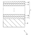
- FIG. 1 is a cross-sectional view of a member 10 such as a cutting tool or a sliding member, for example, and a multilayer hard coating 1 according to the present embodiment is formed on the surface of a base material 2 of the member 10.
- a multilayer hard coating 1 according to the present embodiment is formed on the surface of a base material 2 of the member 10.
- the multilayer hard coating 1 according to this embodiment one or more A layers 11 and one or more B layers 12 are alternately laminated on the surface of the base material 2.
- the atomic ratio X of Si (silicon) in Ti 1-x Si x (B p C q N r ) is set to 0.05 as described above. It is necessary to set to ⁇ 0.4.
- the atomic ratio X of Si in Ti 1-x Si x (B p C q N r ) is less than 0.05, the oxidation resistance is lowered, and the life of the member 10 is not extended.
- the atomic ratio X of Si in Ti 1-x Si x (B p C q N r ) exceeds 0.4, it becomes amorphous and the hardness of the A layer 11 decreases, so that the life of the member 10 is extended. Absent.
- the atomic ratio X of Si in Ti 1-x Si x (B p C q N r ) is preferably 0.1 to 0.3.
- the A layer 11 necessarily contains nitrogen (N), and may optionally contain B (boron) and C (carbon).
- the atomic ratio p of B is 0.3 or less, preferably 0.2 or less, and the atomic ratio q of C is 0.6 or less, preferably 0.4 or less. If both the atomic ratios p and q of B and C are less than this, sufficient hardness can be maintained.
- the thickness of the A layer 11 is preferably as follows in proportion to the thickness of the B layer 12.
- Each of the B layers 12 is Ti 1-agb B a C g N b [where 0.05 ⁇ a ⁇ 0.5, 0.25 ⁇ b ⁇ 0.6, 0 ⁇ g ⁇ 0.5], Si 1-cd C c N d [where 0.2 ⁇ c ⁇ 0.5, 0.25 ⁇ d ⁇ 0.5] and B 1-ef C e N f [where 0.03 ⁇ e ⁇ 0. 25, 0.3 ⁇ f ⁇ 0.55], and when each thickness of the B layer 12 is 2 nm or more and 50 nm or less, each thickness of the A layer 11 is 100 nm or less. Is preferred.
- each of the B layers 12 is made of at least one selected from TiB 2 , SiC and B 4 C
- the thickness of each of the B layers 12 is at least 50 nm.
- the thickness of the A layer 11 is at least 100 nm, and the A layer 11 and the B layer 12 are alternately and repeatedly laminated in this order one or more times on the surface of the substrate 2.
- the A layer 11 can exhibit the effect of increasing the hardness (crystal grain refining effect) by crystal grains being refined by the B layer 12 as will be described later.
- the thickness of the A layer 11 is preferably 100 nm or less as described above.
- the A layer 11 is 10 to 50 nm and 10 to 20 nm.
- the A layer 11 can improve the adhesion between the base material 2 and the B layer 12. Therefore, it is preferable that the lowermost layer of the multilayer hard coating 1 forms the A layer 11 between the surface of the substrate 2 and the lowermost B layer 12 closest to the substrate 2.
- the B layer 12 is one or more selected from the options described as the first embodiment, the B layer 12 is appropriately selected in addition to one selected from these. It can be composed of two types, and all three types.
- the combination relating to the composition is SiCN and TiBN, the case of SiCN and TiBCN, the case of TiBN and BCN, and the case of TiBCN.
- the case of BCN and BCN the case of BCN and SiCN can be mentioned.
- the B layer 12 constituting the multilayer hard coating 1 includes two types of B layers 12, they can be formed by two types of SiCN, TiBCN and BCN, respectively.
- the B layer 12 constituting the multilayer hard coating 1 is For example, a SiCN B layer 12 and a TiBN B layer 12 may be used.
- the multilayer hard coating 1 is laminated on the surface of the base 2 by TiSi (BCN) (A layer 11) / TiBN (B layer 12) / TiSi (BCN) (A layer 11) / SiCN (B layer 12). )become that way.
- the structure in the case where the B layer 12 composed of at least three types of multilayer hard coating 1 is formed on the surface of the substrate 2 is TiSi (BCN) (A layer 11) / TiBN (B layer 12) / TiSi ( BCN) (A layer 11) / SiCN (B layer 12) / TiSi (BCN) (A layer 11) / BCN (B layer 12).
- TiBN and TiBCN are not high in hardness, but boron and nitrogen in the B layer 12 improve lubricity and reduce hardness. To do. However, sufficiently high hardness can be obtained by forming a multilayer structure with the B layer 12 of TiBN or TiBCN having a film thickness of 2 nm to 50 nm, preferably 2 nm to 20 nm and the A layer 11 made of TiSi (BCN). Can do.
- the atomic ratio a of B in Ti 1 -agb B a C g N b is 0.05 to 0.5, preferably 0.2 to 0.4, an excellent lubricating action can be obtained. Life can be extended.
- the atomic ratio a of B in Ti 1-agb B a C g N b is less than 0.05, a lubricating action cannot be obtained, and the hardness also decreases. Therefore, the lifetime of the member 10 is not extended.
- the atomic ratio a of B in Ti 1-agb B a C g N b exceeds 0.5, the hardness decreases. Therefore, the lifetime of the member 10 is not extended.
- the atomic ratio b of N in Ti 1-agb B a C g N b is 0.25 to 0.6, preferably 0.3 to 0.6, an excellent lubricating action can be obtained.
- the atomic ratio b of N in Ti 1 -agb B a C g N b is less than 0.25, a lubricating action cannot be obtained, and the hardness also decreases. Therefore, the lifetime of the member 10 is not extended.
- the atomic ratio b of N in Ti 1-agb B a C g N b exceeds 0.6, the hardness decreases, so the life of the member 10 is not improved.
- Ti 1-agb B a C g N b in the C atomic ratio g is 0.5 or less, it is possible to obtain a high hardness.
- the atomic ratio g of C in Ti 1 -agb B a C g N b exceeds 0.5, unreacted C that is not bonded to a metal element or B precipitates in the B layer 12, and B The hardness of the layer 12 decreases. Therefore, the lifetime of the member 10 is not extended.
- SiCN contains Si and N, so has high affinity with TiSi (BCN) of the A layer 11 and excellent adhesion.
- High hardness can be obtained when the atomic ratio g of C in Si 1 -cd C c N d is 0.2 to 0.5. In both cases where the atomic ratio g of C in Si 1 -cd C c N d is less than 0.2 and exceeds 0.5, the hardness decreases. Therefore, the lifetime of the member 10 is not extended.
- the atomic ratio d of N in Si 1 -cd C c N d is 0.25 to 0.5, preferably 0.3 to 0.5, a lubricating action and high hardness can be obtained.
- the atomic ratio d of N in Si 1-cd C c N d is less than 0.25 and more than 0.5, the hardness decreases. Therefore, the lifetime of the member 10 is not extended.
- the hardness of BCN is not high, but B and N in the BCN layer improve lubricity.
- a sufficiently high hardness can be obtained by forming the A layer 11 containing TiSi (BCN) and the BCN B layer 12 having a thickness of 2 nm to 50 nm, more preferably 2 nm to 20 nm.
- B 1-ef C e N C atomic ratio e of f is 0.03-0.25, and more preferably is 0.1 to 0.25 can be obtained a high hardness. Hardness decreases in any of the case where B 1-ef C e N f in C atomic ratio e exceeds a case and 0.25 of less than 0.03.
- B 1-ef C e N atomic ratio f of N at f 0.3 to 0.55 and more preferably is 0.4 to 0.5 can be obtained lubricating action.
- Hardness decreases in any of the case where B 1-ef C e N f in N atomic ratio f exceeds if and 0.55 of less than 0.3.
- B 1-ef C e N atomic ratio f of N at f is preferably 0.05 to 0.2.
- the thickness of the B layer 12 in the first embodiment described above is 2 nm to 50 nm, more preferably 2 nm to 20 nm.
- the hardness of the A layer 11 can be increased due to the effect of crystal grain refinement.
- the thickness of the B layer 12 is less than 2 nm, the adjacent A layer 11 cannot be controlled well, and the crystal grains of the A layer 12 are not sufficiently refined. Therefore, the hardness of the A layer 12 is lowered, and the hardness of the multilayer hard coating 1 is also lowered accordingly. Therefore, the life of the member 10 may not be extended.
- the thickness of the B layer 12 is 2 nm or more and 20 nm or less, more preferably 5 nm or more and 10 nm or less.
- the plurality of A layers 11 and B layers 12 in the first embodiment are alternately stacked with the respective thicknesses described above.
- the number of repetitions of the A layer 11 and the B layer 12 may be, for example, 5 times or more, but may be 15 times or more, 263 times or more.
- the composition of each A layer 11 constituting the lamination of the multilayer hard coating 1 in the first and / or second embodiment is the same as or different from that of the other laminated A layers 11, and the first and / or second
- Each composition of B layer 12 which constitutes lamination of multilayer hard coat 1 in an embodiment is the same as or different from other laminated B layers 12.
- the multilayer hard coating 1 in the first and / or second embodiment has a structure of A / B1 / A / B2 / A / B3 in addition to A / B / A / B.
- A means A layer
- B means B layer
- B1, B2, and B3 mean B layers having different compositions.
- the composition is different from each of the B layers 12.
- each multilayer hard coating 1 according to the present embodiment includes a structure of A / B1 ′ / B2 ′ / B3 ′ / A.
- B1 ′, B2 ′, and B3 ′ mean layers having compositions different from the above-described composition range of the B layer 12, and the total thicknesses of the B1 ′, B2 ′, and B3 ′ layers are the respective B layers. Within the above range of 12 film thicknesses.
- the A layer 11 can improve the adhesion between the base material 2 and the B layer 12.
- the thickness of the A layer 11 is at least 100 nm. If the thickness of each A layer 11 is less than 100 nm in the second embodiment, the desired effect of the A layer 11 is lost, and the advantages of the multilayer film in adhesion, oxidation resistance and hardness to the substrate 2 are I can't get it.
- the thickness of the A layer 11 is preferably 3000 nm or less.
- the effect of improving the adhesion between the base material 2 and the B layer 12 by the A layer 11 exhibited in the case of the second embodiment is that the A layer 11 is the lowermost layer of the multilayer hard coating 1, that is, the base material 2. It is formed between the surface and the lowermost B layer 12.
- the extremely hard B layer 12 is directly formed on the surface of the substrate 2, so that the adhesion is not improved.
- the B layer 12 is at least one selected from the options of TiB 2 , SiC, and B 4 C described as in the case of the second embodiment, and has a thickness of at least 50 nm. That is, the B layer 12 may be composed of one kind selected from the materials described in the second embodiment, two kinds selected appropriately, or all three kinds. it can. In addition, as a case where the B layer 12 includes two types selected from the options described as the case of the second embodiment, for example, a combination of SiC and TiB 2, a combination of SiC and B 4 C, TiB 2 and B 4 C combinations can be mentioned.
- the B layer 12 can optionally contain nitrogen (N) at least in part.
- the B layer 12 can be arbitrarily formed by using one or more of TiBN, SiCN, BCN, TiB 2 , SiC, and B 4 C.
- the amount of N is 0.5 or less, preferably 0.3 or less, more preferably 0.2 or less in terms of atomic ratio. When the amount of N exceeds 0.5 in atomic ratio, the hardness is lowered and the life of the member 10 is not extended.
- the structure of the multilayer hard coating 1 in which the B layer 12 composed of two types of SiC and TiB 2 is formed is as follows: TiSiN (A layer 11) / TiB 2 (B layer 12) / TiSiN (A Layer 11) / SiC (B layer 12). Further, when the B layer 12 composed of all three types is formed, the structure of TiSiN (A layer 11) / TiB 2 (B layer 12) / TiSiN (A layer 11) / SiC (B Layer 12) / TiSiN (A layer 11) / B 4 C (B layer 12).
- the B layer 12 made of at least one selected from TiBN, SiCN, BCN, TiB 2 , SiC, and B 4 C has extremely high hardness ( ⁇ 40 GPa). Therefore, the wear resistance of the member 10 can be improved by forming the B layer 12.
- the thickness is preferably at least 50 nm as described above. If the thickness of the B layer 12 of the second embodiment is less than 50 nm, the wear resistance of the member 10 may not be improved. Note that the thickness of the B layer 12 is preferably 3000 nm or less.
- the A layer 11 and the B layer 12 in the second embodiment are laminated on the surface of the base material 2 by alternately repeating these layers one or more times in this order.
- the number of repetitions of the lamination of the A layer 11 and the B layer 12 may be one or more, for example, 2 times (total 4 layers), 4 times (total 8 layers), 7 times (total 14 layers) And so on.
- the multilayer hard coating 1 is formed on the surface of the substrate 2 with one A layer 11 and one B layer 12.
- the multilayer hard coating 1 is configured as in the third embodiment shown in FIG. 2, high adhesion to the substrate 2 can be achieved as shown in the examples described later while having a simple configuration. The life of the member 20 can be extended.
- the thickness of the A layer 11 is at least 500 nm.
- the thickness of the B layer 12 is preferably at least 100 nm. Since both high adhesion and oxidation resistance can be reliably obtained, the life of the member 20 can be extended.
- the combination of the A layer 11 and the B layer 12 is a B layer 12 containing SiC or SiCN. If it does in this way, affinity with TiSi (BCN) of A layer 11 will become high with Si contained in B layer 12, and adhesiveness can be raised more.
- the total thickness of the laminated A layer 11 and B layer 12 is 500 nm or more from the viewpoint of extending the life of the member 10.
- the total thickness of the laminated A layer 11 and B layer 12 is less than 500 nm, the portion exhibiting wear resistance becomes thin, and the life of the member 10 is not extended.
- the upper limit of the total thickness of the laminated A layer 11 and B layer 12 is preferably about 5000 nm.
- the base material 2 of the member 30 and the member 40 and the A layer 11 which is the lowest layer of the A layer 11 and the B layer 12 of the multilayer hard coating 1 A predetermined underlayer 13 is preferably formed between them.
- FIG. 3 an example in which the number of repetitions of the lamination of the A layer 11 and the B layer 12 formed on the surface of the substrate 2 is plural is shown.
- 5th Embodiment shown in FIG. 4 what formed A layer 11 and B layer 12 one each on the surface of the base material 2 like the example of FIG. 2 is shown.
- Ti titanium
- Zr zirconium
- Hf hafnium
- examples of the 5A group element include V (vanadium), Nb (niobium), and Ta (tantalum).
- examples of the 6A group element include Cr (chromium), Mo (molybdenum), and W (tungsten).
- the underlayer 13 Preferred examples of such a combination relating to the composition of the underlayer 13 include AlCr (CN), TiAl (CN), TiCrAl (CN), AlCrSi (CN), TiAlSi (CN), and TiCrAlSi (CN). Needless to say, the underlayer 13 selected from these is configured with the above-described atomic ratio.
- the underlayer 13 that can be used in the present invention is not limited thereto.
- a combination of TiAlN, TiN, AlCrN, TiCrAlN, TiAlSiN, AlCrSiN, TiCrAlSiN, NbAlN, or HfAlN may be used.
- M 1-y Al Al in y atomic ratio y from 0.05 to 0.8 (aluminum), preferably 0.1 to A value of 0.6 is preferable.
- M 1-y Al y atomic ratio y of Al in exceeds of less than 0.05 and 0.8 and if the atomic ratio y of Al in the M 1-y Al y is within the numerical range mentioned above In comparison, the hardness and oxidation resistance are slightly inferior, so the effect of extending the life is reduced. Therefore, when the atomic ratio y of Al (aluminum) in the underlayer 13 is in the range of 0.05 to 0.8, there is an effect of extending the life of the member 30 and the member 40.
- M 1-y Al y (B a C b N c O d) are those based on nitride of M for the atomic ratio c of N and 0.5 to 1, optionally B , C, O can be contained.
- the atomic ratio a of B can be 0 to 0.2
- the atomic ratio b of C can be 0 to 0.4
- the atomic ratio d of O (oxygen) can be 0 to 0.2. be able to.
- the thickness of the underlayer 13 is approximately 50 nm or more, it has an effect of improving adhesion, but is preferably 100 nm or more, and more preferably 500 nm or more.
- the thickness of the underlayer 13 is preferably 2000 nm or less.
- the multilayer hard coating 1 described above can be suitably formed by a PVD (Physical Vapor Deposition) method such as sputtering, vapor deposition, arc ion plating, ion beam deposition, or a PVD method in which these are appropriately combined.
- PVD Physical Vapor Deposition
- the B layer forming step (not shown) for forming the A layer 11 consisting of> 0, p + q +
- the multilayer hard coating 1 can be suitably formed by the film forming apparatus 100 shown in FIG.
- the film forming apparatus 100 is an apparatus in which the arc ion plating and sputtering described above are combined.
- the film forming apparatus 100 includes a vacuum arc evaporation source 101 with a target for forming the A layer 11 and a sputtering evaporation source 102 with a target for forming the B layer 12 in the same chamber 103.
- the vacuum arc evaporation source 101 and the sputtering evaporation source 102 are simultaneously discharged while rotating the substrate 2 in the chamber 103, and the A layer 11 and the B layer 12 are laminated on the surface of the substrate 2.
- the substrate 2 can be rotated by being attached to a stage 105 that is rotatably provided in the chamber 103.
- the vacuum arc evaporation source 101 can be suitably used as long as it is a cathode discharge type arc ion plating evaporation source.
- the sputtering evaporation source 102 is also called an unbalanced magnetron sputtering evaporation source, and for example, UBMS 202 manufactured by Kobe Steel can be suitably used.
- the film forming apparatus 100 including two vacuum arc evaporation sources 101 and two sputtering evaporation sources 102 is shown, but three of each may be provided and arranged alternately.
- the adhesion between the A layer 11 and the B layer 12 can be increased. Further, while the substrate 2 is rotated, the vacuum arc evaporation source 101 is discharged to form the A layer 11, and then the discharge of the vacuum arc evaporation source 101 is stopped, the sputtering evaporation source 102 is discharged, and the B layer 12 is discharged. By forming, the A layer 11 and the B layer 12 can be laminated. Note that when the A layer 11 and the B layer 12 are formed, the vacuum arc evaporation source 101 and the sputtering evaporation source 102 may be simultaneously discharged.
- the film forming apparatus 100 includes a vacuum pump (not shown), a gas supply mechanism 104, a stage 105, the heater 106, the bias power source 107, and the sputtering power source 108. And an arc power source 109.
- gases such as Ar, N 2 , and CH 4 are supplied from the gas supply mechanism 104 into the chamber 103 according to the film forming process to be performed.
- MFC1 to MFC4 shown in FIG. 5 are mass flow meters.
- the inside of the chamber 103 is adjusted to a required degree of vacuum by a vacuum pump (not shown).
- the substrate 2 for forming the A layer 11 and the B layer 12 is attached to the stage 105.
- the substrate 2 attached to the stage 105 is heated by the heater 106.
- One sputtering evaporation source 102 is attached with at least one selected from TiB 2 , SiC and B 4 C as a target for forming the B layer 12.
- the other sputtering evaporation source 102 is attached with the same target or a different target selected from the above options.
- a target for forming the A layer 11 and a target for the underlayer 13 are attached to the vacuum arc evaporation source 101 in preparation for forming the underlayer 13.
- one vacuum arc evaporation source 101 has a target made of any one of Ti 0.8 Si 0.2 , Ti 0.95 Si 0.05 , Ti 0.9 Si 0.1 , Ti 0.7 Si 0.3 , Ti 0.6 Si 0.4 and Ti 0.7 Si 0.2 B 0.1. It is attached.
- the other vacuum arc evaporation source 101 includes Ti 0.5 Al 0.5 , Ti, Ti 0.9 Al 0.1 , Ti 0.1 Al 0.9 , Al 0.5 Cr 0.5 , Ti 0.2 Cr 0.2 Al 0.6 , Ti 0.5 Al 0.47 Si 0.03 , A target made of any one of Al 0.45 Cr 0.5 Si 0.05 , Ti 0.2 Cr 0.2 Al 0.55 Si 0.05 , Nb 0.5 Al 0.5 , Hf 0.7 Al 0.3 and (Ti 0.5 Al 0.5 ) C is attached.
- a bias voltage is applied to the stage 105 by the bias power source 107. This bias voltage is applied to the substrate 2 attached to the stage 105.
- the potential of the sputtering evaporation source 102 is controlled by the sputtering power source 108 so that atoms, ions, or clusters are generated from the sputtering evaporation source 102.
- the electric potential of the vacuum arc evaporation source 101 is controlled by the arc power source 109 so that atoms, ions, or clusters are generated from the vacuum arc evaporation source 101.
- the film forming apparatus 100 further includes a filament type ion source 110, a heating AC power source 111 used for AC heating of the ion source 110, and a discharge source for causing the ion source 110 to discharge.
- a filament type ion source 110 used for AC heating of the ion source 110
- a discharge source for causing the ion source 110 to discharge.
- the DC power source 112 is provided, the multilayer hard coating 1 can be formed without using the ion source 110.
- the introduction of C and N into these layers decomposes gases such as N 2 and CH 4 supplied from the gas supply mechanism 104. Is done by doing.
- the multilayer hard coating 1 according to the present invention is a sliding member or a cutting tool that slides on other members, such as jigs and molds for molding, jigs and tools that require wear resistance, and machine parts.
- it When formed on the surface of the base material 2, it has excellent adhesion to the base material 2 and may be excellent in hardness and oxidation resistance.
- 40 can be extended in service life.
- Example A In Example A, first, various films described below were formed on the surface of the substrate.
- the substrate used was a mirror-finished cemented carbide substrate (JIS-P type) and a cemented carbide insert (ADCT 1505 PDFR-HM grade IC28 manufactured by ISCAR).
- the film formed on the former substrate was used for evaluating the hardness, and the film formed on the latter substrate was used for evaluating the tool life.
- the formation of a film on the surface of the substrate is performed by using a plurality of arc ion plating evaporation sources (diameter 100 mm ⁇ ; hereinafter referred to as “AIP evaporation sources”) and a plurality of sputtering evaporation sources (diameter 6 inches ⁇ ; hereinafter referred to as “SP evaporation sources”). ”). Nos. 1 to 3 in Tables 1 to 3 are included in the AIP evaporation source of this film forming apparatus. A base layer target and / or an A layer target is attached in the combinations shown in A1 to A73, and Nos. 1 to 3 in Tables 1 to 3 are attached to the SP evaporation source. A target for the B layer was attached in the combinations shown in A1 to A73. In forming the film, the AIP evaporation source for forming the A layer and the sputter evaporation source for forming the B layer were adjusted alternately.
- the base layer, the A layer, and the B layer were formed with the thickness (nm) shown in Tables 4 to 6, the number of repetitions of the A layer and the B layer, and the total thickness (nm) of the A layer and the B layer.
- “-” In Tables 1 to 3 indicates that no target is attached, and “-” in Tables 4 to 6 indicates that no layer is formed.
- No. A48, A66, A72, and A73 formed a film using a film forming apparatus provided with three sputtering evaporation sources.
- the underlayer was formed, or the A layer and the B layer were alternately formed as shown in Tables 4 to 6 without forming the underlayer.
- the underlayer was formed by performing arc discharge at a current value of 150 A in the presence of N 2 gas (with a smaller amount of CH 4 gas being introduced in No. A62). Then, Ar gas and nitrogen gas were introduced into the chamber at a flow rate ratio of 1: 1 (in the case of No. A15 to A17, a smaller amount of CH 4 gas was introduced), the inside of the chamber was set to 4 Pa, and then attached to the stage While rotating the substrate, arc discharge was performed for a short time to form a thin A layer, and sputter discharge was performed at 2 kW to form a thin B layer.
- the number of repetitions and the thickness of each layer were controlled by changing the rotation speed of the substrate to about 1 to 10 rpm or changing the input power to each evaporation source.
- the hardness was evaluated using a cemented carbide substrate on which a film was formed under the conditions described in A1 to A73.
- a tool life was evaluated using a cemented carbide insert formed with a film under the conditions described in A1 to A73.
- Hardness was measured with a Vickers hardness meter (load 0.25 N).
- the tool life is determined by a composite effect due to various factors such as the hardness and oxidation resistance of the film, the adhesion between the substrate and the film, and the strength of the substrate. Therefore, the tool life was evaluated by a cutting test.
- the cutting test was performed by attaching a cemented carbide insert with a coating to an end mill and dry turning the work material under the following conditions.
- the conditions for dry turning are as follows. ⁇ Conditions for dry turning> Work Material: AISI 316 Cutting speed: 180 m / minute feed: 0.14 mm / blade depth cutting: 4.5 mm Lubrication: Dry
- Table 7 shows the evaluation of hardness and tool life.
- no. Relative values are shown when a cemented carbide insert with a film formed under the conditions of A1 is used as a standard sample and the tool life is 100%. That is, the higher the relative value, the longer the life.
- A49 ⁇ A51, A53, A55 ⁇ A66, A68 ⁇ A71, A73 is, M 1-y Al y ( B a C b N c O d) [ However, 0.05 ⁇ y ⁇ 0.8,0 ⁇ a ⁇ 0.2, 0 ⁇ b ⁇ 0.4, 0.5 ⁇ c ⁇ 1, 0 ⁇ d ⁇ 0.2, M is selected from 4A group element, 5A group element, 6A group element, Si and Y in the periodic table Therefore, the hardness and tool life were even better.
- No. A1 to A6, A12, A21, A22, A25, A26, A28, A29, A32 to A34, A36, A37, A39, A40, A42, A43, A45, A67 satisfy at least one of the requirements of the present invention.
- the result was poor hardness and / or tool life.
- the atomic ratio of B in TiBN forming the B layer is less than 0.2.
- A28 had a low hardness and a short tool life because the atomic ratio of B in TiBN forming the B layer exceeded 0.5.
- the atomic ratio of N in TiBN forming the B layer is less than 0.25.
- A33 had a low hardness and a short tool life because the atomic ratio of N in TiBN forming the B layer exceeded 0.6.
- No. A32 had a low hardness and a short tool life because the atomic ratio of C in TiBCN forming the B layer exceeded 0.5.
- the atomic ratio of C in SiCN forming the B layer is less than 0.2.
- A36 had a low hardness and a short tool life because the atomic ratio of C in SiCN forming the B layer exceeded 0.5.
- No. In A37 the atomic ratio of N in SiCN forming the B layer is less than 0.25.
- A39 had a low hardness and a short tool life because the atomic ratio of N in SiCN forming the B layer exceeded 0.5.
- No. A40 does not contain C in the BCN forming the B layer (the atomic ratio of C is 0).
- A42 had a low hardness and a short tool life because the atomic ratio of C in the BCN forming the B layer exceeded 0.25.
- No. In A43 the atomic ratio of N in BCN forming the B layer is less than 0.3.
- A45 had a low hardness and a short tool life because the atomic ratio of N in the BCN forming the B layer exceeded 0.55.
- No. A67 had a short tool life because the total thickness of the A layer and the B layer was less than 500 nm.
- Example B In Example B, first, various films described below were formed on the surface of the substrate.
- the substrate used was a mirror-finished cemented carbide substrate (JIS-P type) and a cemented carbide insert (ADCT 1505 PDFR-HM grade IC28 manufactured by ISCAR).
- the film formed on the former base material was used for evaluating adhesion, and the film formed on the latter base material was used for evaluating tool life.
- Formation of the film on the surface of the substrate was performed using a film forming apparatus having a plurality of AIP evaporation sources and a plurality of SP evaporation sources, as in Example A. Nos. In Tables 8 and 9 are included in the AIP evaporation source of this film forming apparatus.
- the base layer target and / or the A layer target were attached in the combinations shown in B1 to B60, and Nos. In Tables 8 and 9 were attached to the SP evaporation source.
- B layer targets were attached in combinations shown in B1 to B60.
- the base layer, the A layer, and the B layer were formed with the thickness (nm) shown in Tables 10 and 11, the number of repetitions of the A layer and the B layer, and the total thickness (nm) of the A layer and the B layer. “-” In Tables 8 and 9 indicates that no target is attached, and “-” in Tables 10 and 11 indicates that no layer is formed.
- the base layer was formed, or the A layer and the B layer were formed as shown in Tables 10 and 11 without forming the base layer.
- the underlayer and the A layer were formed by performing arc discharge at a current value of 150 A in the presence of N 2 gas (in the case of No. B14 or No. B15, a smaller amount of CH 4 gas was introduced).
- the B layer was formed by stopping the arc discharge after forming the A layer, reducing the pressure to 0.6 Pa while introducing Ar gas into the chamber, and performing sputtering. When the A layer and the B layer were each two or more layers, the formation of the A layer and the formation of the B layer were repeated.
- the adhesion was evaluated using a cemented carbide substrate on which a film was formed under the conditions described in B1 to B60.
- the tool life was evaluated using a cemented carbide insert formed with a film under the conditions described in B1 to B60.
- the adhesion was evaluated by a scratch test.
- the scratch test was performed by moving a 200 ⁇ m R diamond indenter on a cemented carbide substrate on which a film was formed under the conditions of a load increasing rate of 100 N / min and an indenter moving rate of 10 mm / min.
- the critical load value As the critical load value, the scratch portion was observed with an optical microscope after the scratch test, and the portion where the film was damaged was adopted as the critical load. In Table 12, this is described as adhesion (N).
- the tool life is determined by a composite effect due to various factors such as the hardness and oxidation resistance of the film, the adhesion between the substrate and the film, and the strength of the substrate. Therefore, the tool life was evaluated by a cutting test.
- the cutting test was performed by attaching a cemented carbide insert with a coating to an end mill and dry turning the work material under the following conditions.
- the conditions for dry turning are as follows. ⁇ Conditions for dry turning> Work Material: AISI 316 Cutting speed: 200 m / minute feed: 0.14 mm / blade depth cutting: 4.5 mm Lubrication: Dry
- Table 12 shows the evaluation of adhesion (adhesion force) and tool life.
- adhesion force adhesion force
- tool life 100%. That is, the higher the relative value, the longer the life.
- B33 ⁇ B35, B37, B39 ⁇ B55 is, M 1-y Al y ( B a C b N c O d) [ However, 0.05 ⁇ y ⁇ 0.8,0 ⁇ a ⁇ 0.2,0 ⁇ b ⁇ 0.4, 0.5 ⁇ c ⁇ 1, 0 ⁇ d ⁇ 0.2, M is one or more elements selected from Group 4A elements, Group 5A elements, Group 6A elements, Si and Y] Since it was an underlayer, adhesion and tool life were even better.
- the thickness of the B layer was less than 50 nm. Compared with B1, the adhesion was low and the tool life was short.
- the total thickness of the A layer and the B layer was less than 500 nm. Compared with B1, the adhesion was low and the tool life was short.
- the A layer and the B layer were interchanged to form a film (that is, a SiC layer was formed at the position of the A layer, and a Ti 0.8 Si 0.2 N layer was formed at the position of the B layer). Compared with B1, the adhesion was low and the tool life was short.
- No. B58 has a large amount of N contained in the B layer. Compared with B1, the adhesion was low and the tool life was short.
Landscapes
- Chemical & Material Sciences (AREA)
- Engineering & Computer Science (AREA)
- Organic Chemistry (AREA)
- Materials Engineering (AREA)
- Mechanical Engineering (AREA)
- Metallurgy (AREA)
- Chemical Kinetics & Catalysis (AREA)
- Inorganic Chemistry (AREA)
- Ceramic Engineering (AREA)
- Cutting Tools, Boring Holders, And Turrets (AREA)
- Physical Vapour Deposition (AREA)
- Drilling Tools (AREA)
- Laminated Bodies (AREA)
Priority Applications (6)
| Application Number | Priority Date | Filing Date | Title |
|---|---|---|---|
| EP12857851.5A EP2792765B1 (en) | 2011-12-15 | 2012-12-14 | Multilayer hard film and method for producing same |
| KR1020147015483A KR101625774B1 (ko) | 2011-12-15 | 2012-12-14 | 다층 경질 피막 및 그 제조 방법 |
| US14/365,436 US9340863B2 (en) | 2011-12-15 | 2012-12-14 | Multilayer hard film and method for producing same |
| CN201280061985.8A CN104126025B (zh) | 2011-12-15 | 2012-12-14 | 多层硬质皮膜及其制备方法 |
| IN4404CHN2014 IN2014CN04404A (enExample) | 2011-12-15 | 2012-12-14 | |
| IL233105A IL233105B (en) | 2011-12-15 | 2014-06-12 | Multilayer rigid film and method for its production |
Applications Claiming Priority (4)
| Application Number | Priority Date | Filing Date | Title |
|---|---|---|---|
| JP2011274956A JP5681093B2 (ja) | 2011-12-15 | 2011-12-15 | 多層硬質皮膜 |
| JP2011-274960 | 2011-12-15 | ||
| JP2011-274956 | 2011-12-15 | ||
| JP2011274960A JP5681094B2 (ja) | 2011-12-15 | 2011-12-15 | 積層硬質皮膜 |
Publications (1)
| Publication Number | Publication Date |
|---|---|
| WO2013089254A1 true WO2013089254A1 (ja) | 2013-06-20 |
Family
ID=48612693
Family Applications (1)
| Application Number | Title | Priority Date | Filing Date |
|---|---|---|---|
| PCT/JP2012/082575 Ceased WO2013089254A1 (ja) | 2011-12-15 | 2012-12-14 | 多層硬質皮膜およびその製造方法 |
Country Status (7)
| Country | Link |
|---|---|
| US (1) | US9340863B2 (enExample) |
| EP (1) | EP2792765B1 (enExample) |
| KR (1) | KR101625774B1 (enExample) |
| CN (1) | CN104126025B (enExample) |
| IL (1) | IL233105B (enExample) |
| IN (1) | IN2014CN04404A (enExample) |
| WO (1) | WO2013089254A1 (enExample) |
Cited By (1)
| Publication number | Priority date | Publication date | Assignee | Title |
|---|---|---|---|---|
| EP3165630A4 (en) * | 2014-07-01 | 2018-01-03 | Kabushiki Kaisha Kobe Seiko Sho (Kobe Steel, Ltd.) | Hard coating film |
Families Citing this family (7)
| Publication number | Priority date | Publication date | Assignee | Title |
|---|---|---|---|---|
| JP6131145B2 (ja) | 2013-08-06 | 2017-05-17 | 株式会社神戸製鋼所 | 成膜装置 |
| DE102013019691A1 (de) * | 2013-11-26 | 2015-05-28 | Oerlikon Trading Ag, Trübbach | Hartstoffschicht zur Reduzierung eines Wärmeeintrags in das beschichtete Substrat |
| RU2631572C1 (ru) * | 2016-04-11 | 2017-09-25 | Общество с ограниченной ответственностью "Научно-производственное предприятие "Уралавиаспецтехнология" | Способ нанесения многослойного ионно-плазменного покрытия на поверхность гравюры штампа из жаропрочной стали |
| JP6934772B2 (ja) * | 2017-08-21 | 2021-09-15 | シチズン時計株式会社 | 黒色部材、黒色部材の製造方法および黒色部材を含む時計 |
| GB201802468D0 (en) | 2018-02-15 | 2018-04-04 | Rolls Royce Plc | Coated substrate |
| CN109023263A (zh) * | 2018-08-03 | 2018-12-18 | 河北工程大学 | TiAl/TiAlN/TiCrAlN复合涂层及其制备方法 |
| CN110857465B (zh) * | 2018-08-22 | 2021-11-19 | 赣州澳克泰工具技术有限公司 | 刀具及其制造方法 |
Citations (8)
| Publication number | Priority date | Publication date | Assignee | Title |
|---|---|---|---|---|
| JP2007090483A (ja) | 2005-09-28 | 2007-04-12 | Sumitomo Metal Ind Ltd | 切削工具及びその製造方法 |
| JP3914687B2 (ja) | 2000-04-11 | 2007-05-16 | 住友電工ハードメタル株式会社 | 切削工具とその製造方法 |
| JP2007152542A (ja) * | 2005-11-08 | 2007-06-21 | Mitsubishi Materials Corp | 高硬度鋼の重切削加工で硬質被覆層がすぐれた耐チッピング性を発揮する表面被覆立方晶窒化ほう素基超高圧焼結材料製切削工具 |
| JP2007152544A (ja) * | 2005-11-08 | 2007-06-21 | Mitsubishi Materials Corp | 高硬度鋼の高速切削加工で硬質被覆層がすぐれた耐摩耗性を発揮する表面被覆立方晶窒化ほう素基超高圧焼結材料製切削工具 |
| JP4184691B2 (ja) | 2001-03-28 | 2008-11-19 | セコ ツールズ アクティエボラーグ | 切削工具インサート |
| JP2010207922A (ja) | 2009-03-06 | 2010-09-24 | Mitsubishi Materials Corp | 表面被覆立方晶窒化ほう素基超高圧焼結材料製切削工具 |
| JP2010215966A (ja) * | 2009-03-17 | 2010-09-30 | Smc Corp | 溶損防止用被覆部材 |
| JP2010228032A (ja) | 2009-03-26 | 2010-10-14 | Mitsubishi Materials Corp | 表面被覆立方晶窒化ほう素基超高圧焼結材料製切削工具 |
Family Cites Families (16)
| Publication number | Priority date | Publication date | Assignee | Title |
|---|---|---|---|---|
| JPH04184691A (ja) | 1990-11-20 | 1992-07-01 | Nec Corp | シングルチップマイクロコンピュータ |
| CN100419117C (zh) | 2004-02-02 | 2008-09-17 | 株式会社神户制钢所 | 硬质叠层被膜、其制造方法及成膜装置 |
| WO2006009121A1 (ja) * | 2004-07-23 | 2006-01-26 | Sumitomo Electric Hardmetal Corp. | 圧縮応力の強度分布を有する被膜を備えた表面被覆切削工具 |
| SE0402180D0 (sv) | 2004-09-10 | 2004-09-10 | Sandvik Ab | Deposition of Ti1-xAlxN using Bipolar Pulsed Dual Magnetron Sputtering |
| US7348074B2 (en) * | 2005-04-01 | 2008-03-25 | Oc Oerlikon Balzers Ag | Multilayer hard coating for tools |
| JP4380622B2 (ja) * | 2005-11-04 | 2009-12-09 | 日立ツール株式会社 | 多層皮膜被覆部材及びその製造方法 |
| EP1783245B1 (de) * | 2005-11-04 | 2018-01-24 | Oerlikon Surface Solutions AG, Pfäffikon | Werkzeug oder verschleissteil sowie ein pvd-beschichtungsverfahren zum aufbringen einer oberflächenschicht auf einem werkzeug oder verschleissteil |
| CN100558552C (zh) | 2006-08-09 | 2009-11-11 | 株式会社神户制钢所 | 硬质皮膜及硬质皮膜被覆材 |
| JP4699978B2 (ja) * | 2006-08-09 | 2011-06-15 | 株式会社神戸製鋼所 | 硬質皮膜被覆材 |
| CN102066617B (zh) * | 2008-04-18 | 2014-04-02 | 山特维克知识产权股份有限公司 | 涂层切削工具和其制造方法 |
| JP5297388B2 (ja) * | 2008-04-30 | 2013-09-25 | 住友電気工業株式会社 | 表面被覆切削工具 |
| EP2149624B1 (en) * | 2008-07-31 | 2012-08-08 | Sulzer Metaplas GmbH | Multilayer film-coated member and method for producing it |
| EP2149620B1 (en) * | 2008-07-31 | 2020-04-29 | Oerlikon Surface Solutions AG, Pfäffikon | Multilayer film-coated member and method for producing it |
| JP4900839B2 (ja) * | 2008-07-31 | 2012-03-21 | 日立ツール株式会社 | 多層皮膜被覆部材及びその製造方法 |
| US8911867B2 (en) * | 2009-06-18 | 2014-12-16 | Oerlikon Metaplas Gmbh | Protective coating, a coated member having a protective coating as well as method for producing a protective coating |
| CN102758188A (zh) * | 2011-04-28 | 2012-10-31 | 鸿富锦精密工业(深圳)有限公司 | 镀膜件及其制造方法 |
-
2012
- 2012-12-14 CN CN201280061985.8A patent/CN104126025B/zh not_active Expired - Fee Related
- 2012-12-14 IN IN4404CHN2014 patent/IN2014CN04404A/en unknown
- 2012-12-14 KR KR1020147015483A patent/KR101625774B1/ko not_active Expired - Fee Related
- 2012-12-14 WO PCT/JP2012/082575 patent/WO2013089254A1/ja not_active Ceased
- 2012-12-14 EP EP12857851.5A patent/EP2792765B1/en not_active Not-in-force
- 2012-12-14 US US14/365,436 patent/US9340863B2/en not_active Expired - Fee Related
-
2014
- 2014-06-12 IL IL233105A patent/IL233105B/en active IP Right Grant
Patent Citations (8)
| Publication number | Priority date | Publication date | Assignee | Title |
|---|---|---|---|---|
| JP3914687B2 (ja) | 2000-04-11 | 2007-05-16 | 住友電工ハードメタル株式会社 | 切削工具とその製造方法 |
| JP4184691B2 (ja) | 2001-03-28 | 2008-11-19 | セコ ツールズ アクティエボラーグ | 切削工具インサート |
| JP2007090483A (ja) | 2005-09-28 | 2007-04-12 | Sumitomo Metal Ind Ltd | 切削工具及びその製造方法 |
| JP2007152542A (ja) * | 2005-11-08 | 2007-06-21 | Mitsubishi Materials Corp | 高硬度鋼の重切削加工で硬質被覆層がすぐれた耐チッピング性を発揮する表面被覆立方晶窒化ほう素基超高圧焼結材料製切削工具 |
| JP2007152544A (ja) * | 2005-11-08 | 2007-06-21 | Mitsubishi Materials Corp | 高硬度鋼の高速切削加工で硬質被覆層がすぐれた耐摩耗性を発揮する表面被覆立方晶窒化ほう素基超高圧焼結材料製切削工具 |
| JP2010207922A (ja) | 2009-03-06 | 2010-09-24 | Mitsubishi Materials Corp | 表面被覆立方晶窒化ほう素基超高圧焼結材料製切削工具 |
| JP2010215966A (ja) * | 2009-03-17 | 2010-09-30 | Smc Corp | 溶損防止用被覆部材 |
| JP2010228032A (ja) | 2009-03-26 | 2010-10-14 | Mitsubishi Materials Corp | 表面被覆立方晶窒化ほう素基超高圧焼結材料製切削工具 |
Non-Patent Citations (1)
| Title |
|---|
| See also references of EP2792765A4 |
Cited By (1)
| Publication number | Priority date | Publication date | Assignee | Title |
|---|---|---|---|---|
| EP3165630A4 (en) * | 2014-07-01 | 2018-01-03 | Kabushiki Kaisha Kobe Seiko Sho (Kobe Steel, Ltd.) | Hard coating film |
Also Published As
| Publication number | Publication date |
|---|---|
| CN104126025B (zh) | 2016-08-24 |
| IL233105B (en) | 2018-10-31 |
| US9340863B2 (en) | 2016-05-17 |
| EP2792765B1 (en) | 2018-09-12 |
| IN2014CN04404A (enExample) | 2015-09-04 |
| EP2792765A1 (en) | 2014-10-22 |
| CN104126025A (zh) | 2014-10-29 |
| KR20140090667A (ko) | 2014-07-17 |
| KR101625774B1 (ko) | 2016-05-30 |
| EP2792765A4 (en) | 2015-11-11 |
| US20140363648A1 (en) | 2014-12-11 |
| IL233105A0 (en) | 2014-07-31 |
Similar Documents
| Publication | Publication Date | Title |
|---|---|---|
| KR101625774B1 (ko) | 다층 경질 피막 및 그 제조 방법 | |
| CN104540624B (zh) | 被覆工具 | |
| JP6854241B2 (ja) | 多層pvdコーティングを有する切削工具 | |
| CN105473261B (zh) | 表面被覆工具及其制造方法 | |
| CN100419117C (zh) | 硬质叠层被膜、其制造方法及成膜装置 | |
| CN107848040A (zh) | 表面被覆切削工具及其制造方法 | |
| US10982313B2 (en) | Coated body and method for production of the body | |
| CN111511490A (zh) | 包覆切削工具 | |
| CN101254674B (zh) | 硬质叠层被膜 | |
| KR20140047688A (ko) | 고성능 공구용 나노층 코팅 | |
| JP5395454B2 (ja) | 表面被覆切削工具 | |
| TW201823489A (zh) | 硬質被膜及硬質被膜被覆構件 | |
| JP6491031B2 (ja) | 積層型硬質皮膜および切削工具 | |
| CN112368094A (zh) | 表面被覆切削工具及其制造方法 | |
| JP3460288B2 (ja) | 耐摩耗性に優れた表面被覆部材 | |
| CN101012545A (zh) | 硬质保护膜及其形成方法 | |
| TW201716609A (zh) | 硬質被膜及硬質被膜被覆構件 | |
| JP5681093B2 (ja) | 多層硬質皮膜 | |
| JP5416429B2 (ja) | 表面被覆切削工具 | |
| JP5681094B2 (ja) | 積層硬質皮膜 | |
| JPH07205361A (ja) | 耐摩耗性に優れた表面被覆部材 | |
| JP5651712B2 (ja) | 硬質積層被膜 | |
| JP5734318B2 (ja) | 硬質積層被膜 | |
| WO2014115846A1 (ja) | 耐摩耗性に優れた積層皮膜 | |
| JP6099225B2 (ja) | 硬質潤滑被膜および硬質潤滑被膜被覆工具 |
Legal Events
| Date | Code | Title | Description |
|---|---|---|---|
| 121 | Ep: the epo has been informed by wipo that ep was designated in this application |
Ref document number: 12857851 Country of ref document: EP Kind code of ref document: A1 |
|
| ENP | Entry into the national phase |
Ref document number: 20147015483 Country of ref document: KR Kind code of ref document: A |
|
| WWE | Wipo information: entry into national phase |
Ref document number: 233105 Country of ref document: IL |
|
| WWE | Wipo information: entry into national phase |
Ref document number: 14365436 Country of ref document: US Ref document number: 2012857851 Country of ref document: EP |
|
| NENP | Non-entry into the national phase |
Ref country code: DE |