EP2792765B1 - Multilayer hard film and method for producing same - Google Patents
Multilayer hard film and method for producing same Download PDFInfo
- Publication number
- EP2792765B1 EP2792765B1 EP12857851.5A EP12857851A EP2792765B1 EP 2792765 B1 EP2792765 B1 EP 2792765B1 EP 12857851 A EP12857851 A EP 12857851A EP 2792765 B1 EP2792765 B1 EP 2792765B1
- Authority
- EP
- European Patent Office
- Prior art keywords
- layer
- sic
- hard film
- multilayer hard
- substrate
- Prior art date
- Legal status (The legal status is an assumption and is not a legal conclusion. Google has not performed a legal analysis and makes no representation as to the accuracy of the status listed.)
- Not-in-force
Links
- 238000004519 manufacturing process Methods 0.000 title description 6
- 239000000758 substrate Substances 0.000 claims description 107
- 229910033181 TiB2 Inorganic materials 0.000 claims description 72
- QYEXBYZXHDUPRC-UHFFFAOYSA-N B#[Ti]#B Chemical compound B#[Ti]#B QYEXBYZXHDUPRC-UHFFFAOYSA-N 0.000 claims description 69
- 239000013077 target material Substances 0.000 claims description 39
- 230000008020 evaporation Effects 0.000 claims description 32
- 238000001704 evaporation Methods 0.000 claims description 32
- 238000004544 sputter deposition Methods 0.000 claims description 26
- 238000005520 cutting process Methods 0.000 claims description 21
- 238000009834 vaporization Methods 0.000 claims description 20
- 230000008016 vaporization Effects 0.000 claims description 20
- 229910010060 TiBN Inorganic materials 0.000 claims description 18
- IJGRMHOSHXDMSA-UHFFFAOYSA-N Atomic nitrogen Chemical compound N#N IJGRMHOSHXDMSA-UHFFFAOYSA-N 0.000 claims description 14
- 238000000034 method Methods 0.000 claims description 14
- 229910052751 metal Inorganic materials 0.000 claims description 11
- 239000002184 metal Substances 0.000 claims description 11
- 229910052757 nitrogen Inorganic materials 0.000 claims description 8
- 229910052710 silicon Inorganic materials 0.000 claims description 7
- 229910052727 yttrium Inorganic materials 0.000 claims description 6
- 229910010038 TiAl Inorganic materials 0.000 claims description 3
- 239000010410 layer Substances 0.000 description 419
- 239000010936 titanium Substances 0.000 description 237
- 230000003647 oxidation Effects 0.000 description 20
- 238000007254 oxidation reaction Methods 0.000 description 20
- 239000011651 chromium Substances 0.000 description 17
- 230000015572 biosynthetic process Effects 0.000 description 15
- 230000000694 effects Effects 0.000 description 15
- 239000007789 gas Substances 0.000 description 13
- 239000000463 material Substances 0.000 description 13
- 239000000203 mixture Substances 0.000 description 11
- 229910008484 TiSi Inorganic materials 0.000 description 9
- 239000013078 crystal Substances 0.000 description 9
- 150000002500 ions Chemical class 0.000 description 8
- 230000001965 increasing effect Effects 0.000 description 6
- 229910008482 TiSiN Inorganic materials 0.000 description 5
- 238000010276 construction Methods 0.000 description 5
- 238000011156 evaluation Methods 0.000 description 5
- QRXWMOHMRWLFEY-UHFFFAOYSA-N isoniazide Chemical compound NNC(=O)C1=CC=NC=C1 QRXWMOHMRWLFEY-UHFFFAOYSA-N 0.000 description 5
- XKRFYHLGVUSROY-UHFFFAOYSA-N Argon Chemical compound [Ar] XKRFYHLGVUSROY-UHFFFAOYSA-N 0.000 description 4
- 239000011247 coating layer Substances 0.000 description 4
- 238000010891 electric arc Methods 0.000 description 4
- 239000010955 niobium Substances 0.000 description 4
- 150000004767 nitrides Chemical class 0.000 description 4
- 229910052582 BN Inorganic materials 0.000 description 3
- PZNSFCLAULLKQX-UHFFFAOYSA-N Boron nitride Chemical compound N#B PZNSFCLAULLKQX-UHFFFAOYSA-N 0.000 description 3
- 229910010037 TiAlN Inorganic materials 0.000 description 3
- 239000000956 alloy Substances 0.000 description 3
- 229910045601 alloy Inorganic materials 0.000 description 3
- 229910052799 carbon Inorganic materials 0.000 description 3
- 229910052760 oxygen Inorganic materials 0.000 description 3
- 230000000737 periodic effect Effects 0.000 description 3
- ZOXJGFHDIHLPTG-UHFFFAOYSA-N Boron Chemical compound [B] ZOXJGFHDIHLPTG-UHFFFAOYSA-N 0.000 description 2
- ATJFFYVFTNAWJD-UHFFFAOYSA-N Tin Chemical compound [Sn] ATJFFYVFTNAWJD-UHFFFAOYSA-N 0.000 description 2
- 229910052786 argon Inorganic materials 0.000 description 2
- 229910052796 boron Inorganic materials 0.000 description 2
- 239000013338 boron nitride-based material Substances 0.000 description 2
- 238000004140 cleaning Methods 0.000 description 2
- 239000002131 composite material Substances 0.000 description 2
- 238000010438 heat treatment Methods 0.000 description 2
- 238000005461 lubrication Methods 0.000 description 2
- 238000000465 moulding Methods 0.000 description 2
- 239000012299 nitrogen atmosphere Substances 0.000 description 2
- 238000005240 physical vapour deposition Methods 0.000 description 2
- 239000002356 single layer Substances 0.000 description 2
- OKTJSMMVPCPJKN-UHFFFAOYSA-N Carbon Chemical compound [C] OKTJSMMVPCPJKN-UHFFFAOYSA-N 0.000 description 1
- VYZAMTAEIAYCRO-UHFFFAOYSA-N Chromium Chemical compound [Cr] VYZAMTAEIAYCRO-UHFFFAOYSA-N 0.000 description 1
- ZOKXTWBITQBERF-UHFFFAOYSA-N Molybdenum Chemical compound [Mo] ZOKXTWBITQBERF-UHFFFAOYSA-N 0.000 description 1
- 101100023111 Schizosaccharomyces pombe (strain 972 / ATCC 24843) mfc1 gene Proteins 0.000 description 1
- -1 SiCN and TiBCN Inorganic materials 0.000 description 1
- 229910004205 SiNX Inorganic materials 0.000 description 1
- 229910000831 Steel Inorganic materials 0.000 description 1
- RTAQQCXQSZGOHL-UHFFFAOYSA-N Titanium Chemical compound [Ti] RTAQQCXQSZGOHL-UHFFFAOYSA-N 0.000 description 1
- QCWXUUIWCKQGHC-UHFFFAOYSA-N Zirconium Chemical compound [Zr] QCWXUUIWCKQGHC-UHFFFAOYSA-N 0.000 description 1
- 229910052782 aluminium Inorganic materials 0.000 description 1
- XAGFODPZIPBFFR-UHFFFAOYSA-N aluminium Chemical compound [Al] XAGFODPZIPBFFR-UHFFFAOYSA-N 0.000 description 1
- PNEYBMLMFCGWSK-UHFFFAOYSA-N aluminium oxide Inorganic materials [O-2].[O-2].[O-2].[Al+3].[Al+3] PNEYBMLMFCGWSK-UHFFFAOYSA-N 0.000 description 1
- QVGXLLKOCUKJST-UHFFFAOYSA-N atomic oxygen Chemical compound [O] QVGXLLKOCUKJST-UHFFFAOYSA-N 0.000 description 1
- 229910052804 chromium Inorganic materials 0.000 description 1
- 229910052593 corundum Inorganic materials 0.000 description 1
- 238000000354 decomposition reaction Methods 0.000 description 1
- 230000003247 decreasing effect Effects 0.000 description 1
- 238000000151 deposition Methods 0.000 description 1
- 230000008021 deposition Effects 0.000 description 1
- 238000010586 diagram Methods 0.000 description 1
- 229910003460 diamond Inorganic materials 0.000 description 1
- 239000010432 diamond Substances 0.000 description 1
- 230000005611 electricity Effects 0.000 description 1
- 230000002708 enhancing effect Effects 0.000 description 1
- 229910052735 hafnium Inorganic materials 0.000 description 1
- VBJZVLUMGGDVMO-UHFFFAOYSA-N hafnium atom Chemical compound [Hf] VBJZVLUMGGDVMO-UHFFFAOYSA-N 0.000 description 1
- 238000010348 incorporation Methods 0.000 description 1
- 238000007737 ion beam deposition Methods 0.000 description 1
- 238000007733 ion plating Methods 0.000 description 1
- 238000001755 magnetron sputter deposition Methods 0.000 description 1
- 238000005555 metalworking Methods 0.000 description 1
- 229910052750 molybdenum Inorganic materials 0.000 description 1
- 239000011733 molybdenum Substances 0.000 description 1
- 229910052758 niobium Inorganic materials 0.000 description 1
- GUCVJGMIXFAOAE-UHFFFAOYSA-N niobium atom Chemical compound [Nb] GUCVJGMIXFAOAE-UHFFFAOYSA-N 0.000 description 1
- 230000003287 optical effect Effects 0.000 description 1
- 239000001301 oxygen Substances 0.000 description 1
- 239000002245 particle Substances 0.000 description 1
- 239000010703 silicon Substances 0.000 description 1
- 239000010959 steel Substances 0.000 description 1
- 229910052715 tantalum Inorganic materials 0.000 description 1
- GUVRBAGPIYLISA-UHFFFAOYSA-N tantalum atom Chemical compound [Ta] GUVRBAGPIYLISA-UHFFFAOYSA-N 0.000 description 1
- 229910052719 titanium Inorganic materials 0.000 description 1
- WFKWXMTUELFFGS-UHFFFAOYSA-N tungsten Chemical compound [W] WFKWXMTUELFFGS-UHFFFAOYSA-N 0.000 description 1
- 229910052721 tungsten Inorganic materials 0.000 description 1
- 239000010937 tungsten Substances 0.000 description 1
- 229910052720 vanadium Inorganic materials 0.000 description 1
- LEONUFNNVUYDNQ-UHFFFAOYSA-N vanadium atom Chemical compound [V] LEONUFNNVUYDNQ-UHFFFAOYSA-N 0.000 description 1
- 229910001845 yogo sapphire Inorganic materials 0.000 description 1
- VWQVUPCCIRVNHF-UHFFFAOYSA-N yttrium atom Chemical compound [Y] VWQVUPCCIRVNHF-UHFFFAOYSA-N 0.000 description 1
- 229910052726 zirconium Inorganic materials 0.000 description 1
Images
Classifications
-
- C—CHEMISTRY; METALLURGY
- C23—COATING METALLIC MATERIAL; COATING MATERIAL WITH METALLIC MATERIAL; CHEMICAL SURFACE TREATMENT; DIFFUSION TREATMENT OF METALLIC MATERIAL; COATING BY VACUUM EVAPORATION, BY SPUTTERING, BY ION IMPLANTATION OR BY CHEMICAL VAPOUR DEPOSITION, IN GENERAL; INHIBITING CORROSION OF METALLIC MATERIAL OR INCRUSTATION IN GENERAL
- C23C—COATING METALLIC MATERIAL; COATING MATERIAL WITH METALLIC MATERIAL; SURFACE TREATMENT OF METALLIC MATERIAL BY DIFFUSION INTO THE SURFACE, BY CHEMICAL CONVERSION OR SUBSTITUTION; COATING BY VACUUM EVAPORATION, BY SPUTTERING, BY ION IMPLANTATION OR BY CHEMICAL VAPOUR DEPOSITION, IN GENERAL
- C23C14/00—Coating by vacuum evaporation, by sputtering or by ion implantation of the coating forming material
- C23C14/06—Coating by vacuum evaporation, by sputtering or by ion implantation of the coating forming material characterised by the coating material
- C23C14/0664—Carbonitrides
-
- C—CHEMISTRY; METALLURGY
- C23—COATING METALLIC MATERIAL; COATING MATERIAL WITH METALLIC MATERIAL; CHEMICAL SURFACE TREATMENT; DIFFUSION TREATMENT OF METALLIC MATERIAL; COATING BY VACUUM EVAPORATION, BY SPUTTERING, BY ION IMPLANTATION OR BY CHEMICAL VAPOUR DEPOSITION, IN GENERAL; INHIBITING CORROSION OF METALLIC MATERIAL OR INCRUSTATION IN GENERAL
- C23C—COATING METALLIC MATERIAL; COATING MATERIAL WITH METALLIC MATERIAL; SURFACE TREATMENT OF METALLIC MATERIAL BY DIFFUSION INTO THE SURFACE, BY CHEMICAL CONVERSION OR SUBSTITUTION; COATING BY VACUUM EVAPORATION, BY SPUTTERING, BY ION IMPLANTATION OR BY CHEMICAL VAPOUR DEPOSITION, IN GENERAL
- C23C14/00—Coating by vacuum evaporation, by sputtering or by ion implantation of the coating forming material
- C23C14/06—Coating by vacuum evaporation, by sputtering or by ion implantation of the coating forming material characterised by the coating material
-
- C—CHEMISTRY; METALLURGY
- C23—COATING METALLIC MATERIAL; COATING MATERIAL WITH METALLIC MATERIAL; CHEMICAL SURFACE TREATMENT; DIFFUSION TREATMENT OF METALLIC MATERIAL; COATING BY VACUUM EVAPORATION, BY SPUTTERING, BY ION IMPLANTATION OR BY CHEMICAL VAPOUR DEPOSITION, IN GENERAL; INHIBITING CORROSION OF METALLIC MATERIAL OR INCRUSTATION IN GENERAL
- C23C—COATING METALLIC MATERIAL; COATING MATERIAL WITH METALLIC MATERIAL; SURFACE TREATMENT OF METALLIC MATERIAL BY DIFFUSION INTO THE SURFACE, BY CHEMICAL CONVERSION OR SUBSTITUTION; COATING BY VACUUM EVAPORATION, BY SPUTTERING, BY ION IMPLANTATION OR BY CHEMICAL VAPOUR DEPOSITION, IN GENERAL
- C23C14/00—Coating by vacuum evaporation, by sputtering or by ion implantation of the coating forming material
- C23C14/22—Coating by vacuum evaporation, by sputtering or by ion implantation of the coating forming material characterised by the process of coating
- C23C14/24—Vacuum evaporation
- C23C14/32—Vacuum evaporation by explosion; by evaporation and subsequent ionisation of the vapours, e.g. ion-plating
- C23C14/325—Electric arc evaporation
-
- C—CHEMISTRY; METALLURGY
- C23—COATING METALLIC MATERIAL; COATING MATERIAL WITH METALLIC MATERIAL; CHEMICAL SURFACE TREATMENT; DIFFUSION TREATMENT OF METALLIC MATERIAL; COATING BY VACUUM EVAPORATION, BY SPUTTERING, BY ION IMPLANTATION OR BY CHEMICAL VAPOUR DEPOSITION, IN GENERAL; INHIBITING CORROSION OF METALLIC MATERIAL OR INCRUSTATION IN GENERAL
- C23C—COATING METALLIC MATERIAL; COATING MATERIAL WITH METALLIC MATERIAL; SURFACE TREATMENT OF METALLIC MATERIAL BY DIFFUSION INTO THE SURFACE, BY CHEMICAL CONVERSION OR SUBSTITUTION; COATING BY VACUUM EVAPORATION, BY SPUTTERING, BY ION IMPLANTATION OR BY CHEMICAL VAPOUR DEPOSITION, IN GENERAL
- C23C14/00—Coating by vacuum evaporation, by sputtering or by ion implantation of the coating forming material
- C23C14/22—Coating by vacuum evaporation, by sputtering or by ion implantation of the coating forming material characterised by the process of coating
- C23C14/34—Sputtering
-
- C—CHEMISTRY; METALLURGY
- C23—COATING METALLIC MATERIAL; COATING MATERIAL WITH METALLIC MATERIAL; CHEMICAL SURFACE TREATMENT; DIFFUSION TREATMENT OF METALLIC MATERIAL; COATING BY VACUUM EVAPORATION, BY SPUTTERING, BY ION IMPLANTATION OR BY CHEMICAL VAPOUR DEPOSITION, IN GENERAL; INHIBITING CORROSION OF METALLIC MATERIAL OR INCRUSTATION IN GENERAL
- C23C—COATING METALLIC MATERIAL; COATING MATERIAL WITH METALLIC MATERIAL; SURFACE TREATMENT OF METALLIC MATERIAL BY DIFFUSION INTO THE SURFACE, BY CHEMICAL CONVERSION OR SUBSTITUTION; COATING BY VACUUM EVAPORATION, BY SPUTTERING, BY ION IMPLANTATION OR BY CHEMICAL VAPOUR DEPOSITION, IN GENERAL
- C23C28/00—Coating for obtaining at least two superposed coatings either by methods not provided for in a single one of groups C23C2/00 - C23C26/00 or by combinations of methods provided for in subclasses C23C and C25C or C25D
- C23C28/04—Coating for obtaining at least two superposed coatings either by methods not provided for in a single one of groups C23C2/00 - C23C26/00 or by combinations of methods provided for in subclasses C23C and C25C or C25D only coatings of inorganic non-metallic material
- C23C28/042—Coating for obtaining at least two superposed coatings either by methods not provided for in a single one of groups C23C2/00 - C23C26/00 or by combinations of methods provided for in subclasses C23C and C25C or C25D only coatings of inorganic non-metallic material including a refractory ceramic layer, e.g. refractory metal oxides, ZrO2, rare earth oxides
-
- C—CHEMISTRY; METALLURGY
- C23—COATING METALLIC MATERIAL; COATING MATERIAL WITH METALLIC MATERIAL; CHEMICAL SURFACE TREATMENT; DIFFUSION TREATMENT OF METALLIC MATERIAL; COATING BY VACUUM EVAPORATION, BY SPUTTERING, BY ION IMPLANTATION OR BY CHEMICAL VAPOUR DEPOSITION, IN GENERAL; INHIBITING CORROSION OF METALLIC MATERIAL OR INCRUSTATION IN GENERAL
- C23C—COATING METALLIC MATERIAL; COATING MATERIAL WITH METALLIC MATERIAL; SURFACE TREATMENT OF METALLIC MATERIAL BY DIFFUSION INTO THE SURFACE, BY CHEMICAL CONVERSION OR SUBSTITUTION; COATING BY VACUUM EVAPORATION, BY SPUTTERING, BY ION IMPLANTATION OR BY CHEMICAL VAPOUR DEPOSITION, IN GENERAL
- C23C28/00—Coating for obtaining at least two superposed coatings either by methods not provided for in a single one of groups C23C2/00 - C23C26/00 or by combinations of methods provided for in subclasses C23C and C25C or C25D
- C23C28/04—Coating for obtaining at least two superposed coatings either by methods not provided for in a single one of groups C23C2/00 - C23C26/00 or by combinations of methods provided for in subclasses C23C and C25C or C25D only coatings of inorganic non-metallic material
- C23C28/044—Coating for obtaining at least two superposed coatings either by methods not provided for in a single one of groups C23C2/00 - C23C26/00 or by combinations of methods provided for in subclasses C23C and C25C or C25D only coatings of inorganic non-metallic material coatings specially adapted for cutting tools or wear applications
-
- C—CHEMISTRY; METALLURGY
- C23—COATING METALLIC MATERIAL; COATING MATERIAL WITH METALLIC MATERIAL; CHEMICAL SURFACE TREATMENT; DIFFUSION TREATMENT OF METALLIC MATERIAL; COATING BY VACUUM EVAPORATION, BY SPUTTERING, BY ION IMPLANTATION OR BY CHEMICAL VAPOUR DEPOSITION, IN GENERAL; INHIBITING CORROSION OF METALLIC MATERIAL OR INCRUSTATION IN GENERAL
- C23C—COATING METALLIC MATERIAL; COATING MATERIAL WITH METALLIC MATERIAL; SURFACE TREATMENT OF METALLIC MATERIAL BY DIFFUSION INTO THE SURFACE, BY CHEMICAL CONVERSION OR SUBSTITUTION; COATING BY VACUUM EVAPORATION, BY SPUTTERING, BY ION IMPLANTATION OR BY CHEMICAL VAPOUR DEPOSITION, IN GENERAL
- C23C28/00—Coating for obtaining at least two superposed coatings either by methods not provided for in a single one of groups C23C2/00 - C23C26/00 or by combinations of methods provided for in subclasses C23C and C25C or C25D
- C23C28/40—Coatings including alternating layers following a pattern, a periodic or defined repetition
- C23C28/42—Coatings including alternating layers following a pattern, a periodic or defined repetition characterized by the composition of the alternating layers
-
- C—CHEMISTRY; METALLURGY
- C23—COATING METALLIC MATERIAL; COATING MATERIAL WITH METALLIC MATERIAL; CHEMICAL SURFACE TREATMENT; DIFFUSION TREATMENT OF METALLIC MATERIAL; COATING BY VACUUM EVAPORATION, BY SPUTTERING, BY ION IMPLANTATION OR BY CHEMICAL VAPOUR DEPOSITION, IN GENERAL; INHIBITING CORROSION OF METALLIC MATERIAL OR INCRUSTATION IN GENERAL
- C23C—COATING METALLIC MATERIAL; COATING MATERIAL WITH METALLIC MATERIAL; SURFACE TREATMENT OF METALLIC MATERIAL BY DIFFUSION INTO THE SURFACE, BY CHEMICAL CONVERSION OR SUBSTITUTION; COATING BY VACUUM EVAPORATION, BY SPUTTERING, BY ION IMPLANTATION OR BY CHEMICAL VAPOUR DEPOSITION, IN GENERAL
- C23C28/00—Coating for obtaining at least two superposed coatings either by methods not provided for in a single one of groups C23C2/00 - C23C26/00 or by combinations of methods provided for in subclasses C23C and C25C or C25D
- C23C28/40—Coatings including alternating layers following a pattern, a periodic or defined repetition
- C23C28/44—Coatings including alternating layers following a pattern, a periodic or defined repetition characterized by a measurable physical property of the alternating layer or system, e.g. thickness, density, hardness
-
- Y—GENERAL TAGGING OF NEW TECHNOLOGICAL DEVELOPMENTS; GENERAL TAGGING OF CROSS-SECTIONAL TECHNOLOGIES SPANNING OVER SEVERAL SECTIONS OF THE IPC; TECHNICAL SUBJECTS COVERED BY FORMER USPC CROSS-REFERENCE ART COLLECTIONS [XRACs] AND DIGESTS
- Y10—TECHNICAL SUBJECTS COVERED BY FORMER USPC
- Y10T—TECHNICAL SUBJECTS COVERED BY FORMER US CLASSIFICATION
- Y10T428/00—Stock material or miscellaneous articles
- Y10T428/24—Structurally defined web or sheet [e.g., overall dimension, etc.]
- Y10T428/24942—Structurally defined web or sheet [e.g., overall dimension, etc.] including components having same physical characteristic in differing degree
- Y10T428/2495—Thickness [relative or absolute]
- Y10T428/24967—Absolute thicknesses specified
- Y10T428/24975—No layer or component greater than 5 mils thick
Definitions
- the present invention relates to a multilayer hard film including at least one layer of Ti 1-x Si x (B p C q N r ) formed on a surface of a substrate of a slide member over which other member slides or a cutting tool for use in metal cutting processes.
- the slide member includes, for example, a jig, and a mechanical component such as a die for molding and a punch each requiring wear resistance.
- the present invention relates to a method for producing the multilayer hard film.
- layers (or films) stacked of, for example, TiB 2 , B 4 C, SiC and the like are commonly formed on a surface of a substrate of a slide member or a metal cutting tool. Since a film made of a material such as TiB2, B 4 C and SiC has extremely high hardness (approximately 40 GPa), such a film formed on the surface of the slide member or of the metal cutting tool is called, for example, a hard film.
- a film formed by stacking a plurality of layers made of the above materials is particularly called a multilayer hard film.
- various techniques of forming a hard film or a multilayer hard film using at least one layer made of TiB 2 , B 4 C, SiC, and the like are disclosed in Patent Literatures 1 - 6.
- Patent Literature 1 discloses formation of a multilayer hard film made by stacking a TiB 2 layer, a two-phase mixed layer of TiB 2 and TiN phases, and a TiAlN layer in this order on a surface of a tool base formed of a cubic boron nitride-based material sintered under an ultrahigh pressure.
- Patent Literature 2 discloses formation of a hard film on a surface of a base, where the hard film contains at least one TiB 2 sublayer having a fibrous microstructure in which fibrous particles having a predetermined diameter and a predetermined length are oriented in the direction perpendicular to the surface of the base.
- Patent Literature 3 discloses formation of a multilayer hard film made by stacking a BCN layer, a B 4 C layer, and a TiAlN layer in this order on a surface of a tool base formed of a cubic boron nitride-based material sintered under an ultrahigh pressure.
- Patent Literature 4 discloses formation of a hard film made of SiC on a surface of a base.
- the main component of the hard film is a nitride or a carbonitride of at least one kind of element selected from the Group 4A, Group 5A and Group 6A elements and Al.
- Patent Literature 6 discloses a surface-coated cutting tool which is made of cubic boron nitride-based ultra high pressure sintered material, and has a hard coated layer showing excellent wear resistance in high speed cutting of high hardness steel.
- Patent Literatures 1 - 6 have high hardness and the wear resistance as well as other preferable properties via improvement of a stacked film.
- the difference in hardness between the substrate and the hard film leads to poor adhesion of the hard film to the substrate, which frequently terminates in the hard film peeling off the surface of the substrate. This results in a major drawback of a shortened lifetime of the cutting tool.
- Patent Literature 1 an attempt is made to improve the adhesion of hard films to substrates and to elongate the lifetime of the slide member by using the cubic boron nitride-based ultra high pressure-sintered material. Additionally, in Patent Literature 3, an additional attempt is made to further improve the adhesion of the film to the surface of the base which constitutes the tool and is formed of the cubic boron nitride-based ultra high pressure-sintered material, and elongate the lifetime of the base constituting the tool by forming the BCN layer between the B 4 C layer and the surface of the base (as a slide member) constituting the tool. Further, in Patent Literature 5, an attempt is made to improve the adhesion of the hard film and to elongate the lifetime of the slide member by including TiB 2 , B 4 C, SiC, and the like in the hard film.
- an object of the present invention is to provide a multilayer hard film which sufficiently elongates a lifetime of a substrate included in a slide member or a metal working cutting tool.
- the above mentioned method allows the multilayer hard coating layer described in section (i) to be formed on the surface of the substrate.
- the multilayer hard film capable of elongating the lifetime of the member.
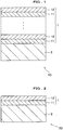
- a multilayer hard film is provided by the present invention, and first and second embodiments will be shown in FIG. 1 .
- FIG. 1 schematically shows a cross-section of a member 10 such as a metal cutting tool or a slide member.
- a multilayer hard film 1 of the first and second embodiments is formed on a surface of a substrate 2 included in the member 10.
- a layer 11 (layer A) and a layer 12 (layer B) are alternately stacked one over the other to form a stack including the plurality of layers 11 and 12 over the surface of the substrate 2.
- Layer 11 will be referred to as layer A 11 and layer 12 will be referred to as layer B12.
- each layer A 11 is needed to have high hardness and high oxidation resistance.
- the atomic ratio "x" of Si (silicon) in Ti 1-x Si x (B p C q N r ) should be set in 0.05 to 0.4. If the atomic ratio "x" of Si in Ti 1-x Si x (B p C q N r ) is less than 0.05, the oxidation resistance is too low to elongate the lifetime of the member 10. Further, if the atomic ratio "x" of Si in Ti 1-x Si x (B p C q N r ) exceeds 0.4, the layer A 11 becomes amorphous and thereby decreasing the hardness of the layer A 11.
- the atomic ratio "x" of Si in Ti 1-x Si x (B p C q N r ) is set in 0.1 to 0.3.
- the layer A 11 must contain N (nitrogen), and optionally may contain B (boron) and/or C (carbon).
- B boron
- C carbon
- the atomic ratio "p" of B is 0.3 or less, and more preferably 0.2 or less.
- the atomic ratio "q" of C is 0.6 or less, and more preferably 0.4 or less.
- a thickness of the layer A 11 is set as proportional to a thickness of the layer B 12.
- the respective layers B 12 are formed of at least one of Ti 1-a-g-b B a C g N b , Si 1-c-d C c N d , and B 1-e-f C e N f with a thickness of 2 nm to 50 nm, where 0.05 ⁇ a ⁇ 0.5, 0.25 ⁇ b ⁇ 0.6, 0.2 ⁇ c ⁇ 0.5, 0.25 ⁇ d ⁇ 0.5, 0.03 ⁇ e ⁇ 0.25, 0.3 ⁇ f ⁇ 0.55 and 0 ⁇ g ⁇ 0.5, it is preferable that each thickness of the layers A is set in 100 nm or less.
- a thickness of the respective layers B 12 is set as at least 50 nm, and a thickness of the respective layers 11 A is set as at least 100 nm. Further, the layer 11 A and the layer B 12 are alternately stacked one over the other in this order one or more times to form the stack on the surface of the substrate 2.
- layer A 11 is formed on the near amorphous layer B 12. Consequently, layer B 12 has micronization effect on the crystal grains in each layer A 11 and thus increasing the hardness of each layer A 11 (referred to as "micronization effect").
- the thickness of each layer A 11 should preferably be 100 nm or less as mentioned above in order to maintain a ratio between the total thickness of the layers A 11 and the total thickness of the layers B 12 at a predetermined value.
- each layer 11 A is preferably set in 10 nm to 50 nm, and more preferably 10 nm to 20 nm.
- the formation of the layer A 11 can improve the adhesion of the layer B 12 to the substrate 2. Therefore, it is preferable that the undermost layer of the multilayer hard film 1 be formed of the layer A 11 between the surface of the substrate 2 and the undermost layer B 12 located closest to the substrate 2.
- each layer B 12 is formed of one or more components selected from the group as described above. Therefore, each layer B 12 may be formed of one component, two components appropriately selected from the group, or all the three components therefrom.
- the layer B 12 when the layer B 12 is formed of two components selected from the group as described in the first embodiment, such a combination includes: SiCN and TiBN, SiCN and TiBCN, TiBN and BCN, TiBCN and BCN, or BCN and SiCN.
- the layers B 12 constructing the multilayer hard film 1 include two types of layers B 12, such layers B may be respectively formed of two components selected from the group of SiCN, TiBCN and BCN.
- the layers B 12 constructing the multilayer hard film 1 may be formed of a layer B 12 made of SiCN and a layer 12 B made of TiBN.
- the stack of the multilayer hard film 1 may be constructed by a pair of layer A 11 of TiSi(BCN) and a layer B 12 of TiBN, a pair of layer A 11 of TiSi(BCN) and a layer B 12 of SiCN in this order over the surface of the substrate 2.
- the stack may be formed by a pair of layer A 11 of TiSi(BCN) and a layer B 12 of TiBN, a pair of a layer A 11 of TiSi(BCN) and a layer B 12 of SiCN, pair of a layer A 11 of TiSi(BCN) and a layer B 12 of BCN in this order over the surface of the substrate 2.
- TiBN and TiBCN constituting the layer B 12 actually TiBN and TiBCN do not have high hardness.
- boron and nitrogen elements included in such a layer B 12 improve lubricity, while such elements decrease the hardness. Nonetheless, it is possible to make a film sufficiently hard, if a multilayer structure of the film is formed via alternately stacking a layer B 12 made of TiBN or TiBCN having a thickness from 2 nm to 50 nm, preferably from 2 nm to 20 nm, and a layer 11 A made of TiSi(BCN) one another.
- the atomic ratio "a" of B in Ti 1-a-g-b B a C g N b is 0.2 to 0.5, preferably 0.2 to 0.4, it is possible to achieve excellent lubricity, which allows increase in the lifetime of the member 10.
- the atomic ratio "a" of B in Ti 1-a-g-b B a C g N b is less than 0.05, satisfactory lubricity is not achieved and the hardness becomes lower, which results in decrease in the lifetime of the member 10.
- the atomic ratio "a" of B in Ti 1-a-g-b B a C g N b exceeds 0.5, the hardness becomes lower, which results in decrease in the lifetime of the member 10.
- the atomic ratio "b" of N in Ti 1-a-g-b B a C g N b is 0.25 to 0.6, preferably 0.3 to 0.6, it is possible to achieve excellent lubricity.
- the atomic ratio "b" of N in Ti 1-a-g-b B a C g N b is less than 0.25, satisfactory lubricity is not achieved and the hardness becomes lower, which results in decrease in the lifetime of the member 10.
- the atomic ratio "b" of N in Ti 1-a-g-b B a C g N b exceeds 0.6, the hardness becomes lower, which results in no improvement for the lifetime of the member 10.
- SiCN contains Si and N. Therefore, SiCN has high affinity for TiSi(BCN) constructing the layer A 11 and excellent adhesion to the layer A 11.
- the atomic ratio "c" of C in Si 1-c-d C c N d is 0.2 to 0.5, it is possible to achieve high hardness. In contrast, if the atomic ratio "c" of C in Si 1-c-d C c N d is out of the range from 0.2 to 0.5, the hardness becomes lower, which results in no elongation in the lifetime of the member 10.
- the atomic ratio "d" of N in Si 1-c-d C c N d is 0.25 to 0.5, preferably 0.3 to 0.5, it is possible to achieve satisfactory lubricity and high hardness.
- the atomic ratio "d" of N in Si 1-c-d C c N d is out of the range from 0.25 to 0.5, the hardness becomes lower, whereby the lifetime of the member 10 is not to be elongated.
- BCN does not have high hardness, while a B element and an N element in the BCN layer improve lubricity. Nevertheless, it is possible to achieve sufficiently high hardness by alternately stacking the layer B 12 made of BCN having a thickness of 2 nm to 50 nm, preferably 2 nm to 20 nm, and the layer A 11 including TiSi (BCN) one another.
- the atomic ratio "f" of N in B 1-e-f C e N f is 0.3 to 0.55, preferably 0.4 to 0.5, it is possible to achieve satisfactory lubricity.
- the atomic ratio "f" of N in B 1-e-f C e N f is out of the range from 0.3 to 0.55, the hardness becomes lower, and the lubricity can become insufficient. This results in no elongation in the lifetime of the member 10.
- each layer B 12 in the first embodiment is 2 nm to 50 nm, preferably 2 nm to 20 nm, as mentioned hereinbefore. Formation of each layer B 12 with the thickness in the above range allows the hardness of the layer A to be high as a result of the micronization effect of the crystal grains in the layer A 11. If the thickness of each layer B 12 falls below 2 nm, the crystal growth in the layer A 11 adjacent to the layer B is not sufficiently controlled, whereby the crystal grains in the layer A 11 is not sufficiently micronized. Therefore, the hardness of the layer A 11 becomes lower, and accordingly the hardness of the multilayer hard film 1 also becomes lower. Consequently, the lifetime of the member 10 is not elongated.
- each layer B 12 exceeds 50 nm, the total ratio of the layers B thickness to the layers A thickness in the stack becomes larger, leading to decrease in the adhesion and oxidation resistance of the multilayer hard film 1. This is likely to result in no elongation of the lifetime of the member 10. It is preferable that the thickness of each layer B 12 be 2 nm to 20 nm, more preferably 5 nm to 10 nm.
- the plurality of layers A 11 and layers B 12 in the first embodiment respectively having the thicknesses explained above form a stack by alternately stacking the layers A 11 and the layers B 12 one over the other.
- the number of repetitions of forming a pair of a layer A 11 and a layer B 12 (i.e., the number of pairs of a layer A 11 and a layer B 12) in the multilayer hard film 1 may be, for example, five or more. That is, the number of pairs may be 15 or more, or 263 or more.
- the composition of the respective layers A 11 constructing the stack of the multilayer hard film 1 may be the same or different each other in the stack.
- the composition of the respective layers B 12 constructing the stack of the multilayer hard film 1 according to the first and/or second embodiment may be the same or different each other in the stack.
- the multilayer hard film 1 according to the first and/or second embodiments may have the structure of A/B/A/B, or A/B1/A/B2/A/B3, where A denotes a layer A, B denotes a layer B , and B1, B2 and B3 denote layers B respectively having different compositions.
- the composition of B1, B2 and B3 is different from the composition of each layer B 12.
- each multilayer hard film 1 may include the structure of A/B1'/B2'/B3'/A, where B1', B2' and B3' denote layers respectively having a different range of composition from the range of composition of the layer B 12 defined above. Furthermore, the total thickness of the layers B1', B2' and B3' is within the aforementioned range of the thickness of the B layers 12.
- the layers A 11 improve the adhesion of the layers B 12 to the substrate 2.
- the thickness of the respective layers A is set in at least 100 nm in order to maintain a ratio of the total thicknesses between the layers A 11 and the layers B 12 in the stack. If the thickness of each layer A 11 is less than 100 nm in the second embodiment, desired effect of the layers A 11 in the stack is diluted, which prevents the excellent effect of a multilayer film on the hardness, oxidation resistance and adhesion to the substrate from being exerted.
- the thickness of each layer A 11 be 3000 nm or less.
- the effect of improving the adhesion of the layer B 12 to the substrate 2 via the layer A 11 in the second embodiment is exerted by forming a layer A 11 as the bottom layer of the multilayer hard film 1, that is, as the layer located between the undermost layer of the layers B 12 and the substrate 2. If such a layer A 11 is not formed directly on the surface of the substrate 2 in the second embodiment, an extremely hard layer B 12 is to be formed directly on the surface of the substrate 2. This results in no improvement of the adhesion of the layer B 12.
- Each layer B 12 of the second embodiment is formed of at least one selected from TiB 2 , SiC, and B 4 C and has a thickness of at least 50 nm. That is, each layer B 12 may be formed by using one, appropriately selected two, or all of the materials described in the second embodiment.
- the layer B 12 is formed of two components selected as in the second embodiment, such two components include the combination of SiC and TiB 2 , SiC and B 4 C, or TiB 2 and B 4 C.
- the layers B 12 may optionally and at least partially contain nitrogen (N).
- the layers B 12 may optionally be formed by using one or more components selected from TiBN, SiCN, BCN, TiB 2 , SiC, and B 4 C.
- the atomic ratio of N may be 0.5 or less, preferably 0.3 or less, and more preferably 0.2 or less. If the atomic ratio of N is more than 0.5, the hardness becomes lower, resulting in no elongation of the lifetime of the member 10.
- the stack may be constructed on the surface of the substrate, by stacking a layer A 11 of TiSiN / a layer B 12 of TiB 2 / a layer A 11 of TiSiN / a layer B 12 of SiC in this order.
- the stack may be constructed on the surface of the substrate 2 by stacking a layer A 11 of TiSiN / a layer B 12 of TiB 2 / a layer A 11 of TiSiN / a layer B 12 of SiC / a layer A 11 of TiSiN / a layer B 12 of B 4 C in this order.
- the layer B 12 formed of at least one selected from TiBN, SiCN, BCN, TiB 2 , SiC and B 4 C has extremely high hardness (around 40 GPa). Therefore, it is possible to improve the wear resistance of the member 10 by forming the layer B 12.
- the thickness of each layer B 12 of the second embodiment be at least 50 nm. If the thickness of each layer B 12 is less than 50 nm, the wear resistance of the member 10 is likely not to be improved.
- the thickness of each B layer is 3000 nm or less.
- a stack of the second embodiment is formed by alternately stacking a layer A 11 and a layer B 12 one or more times in this order over the surface of the substrate 2.
- the number of pairs of the layer A 11 and the layer B 12 is at least one. For example, two times (or total of four layers), four times (or total of eight layers), or seven times (or total of fourteen layers) may be applicable.
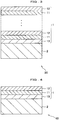
- FIG. 2 A third embodiment of the present invention is illustrated in FIG. 2 .
- the multilayer hard film 1 is stacked formed of a single pair of layers A 11 and B 12 over the surface of the substrate 2.
- the multilayer hard film 1 in the third embodiment has a structure as illustrated in FIG. 2 , such a simple structure is capable of realizing high adhesion to the substrate 2, and elongating a lifetime of the member 20, as indicated later by Examples.
- the thickness of the layer A 11 is preferably at least 500 nm, and the thickness of the layer B 12 is preferably at least 100 nm.
- the multilayer hard film 1 of FIG. 2 reliably achieves both high adhesion and high oxidation resistance, which allows the lifetime of the member 20 to be elongated.
- a combination of the layer A 11 and the layer B 12 includes a layer B 12 containing SiC or SiCN.
- a layer B 12 enables the affinity to TiSi(BCN) in the layer A 11 to be enhanced due to Si contained in the layer B 12, whereby the adhesion is further improved.
- the total thickness of the stack formed of the layer A 11 and the layer B 12 in the multilayer hard film 1 is set in 500 nm or more, in view of the elongation of the lifetime of the member 10. If the total thickness of the stacked layers A 11 and B 12 is less than 500 nm, an total thickness of the layers exerting the wear resistant effect becomes too thin to elongate the lifetime of the member 10. The desired effect of elongating the lifetime of the members 10 and 20 is further enhanced as the total thickness of the stack formed of the layers A 11 and B 12 increases. Nevertheless, this effect diminishes, if the total thickness of the stack is beyond approximately 10 ⁇ m. Accordingly, it is preferable that the upper limit of the total thickness of the stacked layers A 11 and B 12 be approximately 5000 nm.
- a predetermined underlying layer 13 is formed between the undermost layer A 11 of the multilayer hard film 1 and the substrate 2 in the member 30 or the member 40 as respectively illustrated in FIGS. 3 and 4 .
- shown is a stack formed by alternately stacking a layer A 11 and a layer B 12 multi times over the surface of the substrate 2.
- shown is a stack formed of only a pair of layers A 11 and B 12 over the surface of the substrate 2 similarly as shown in FIG. 2 .
- the underlying layer 13 may be formed of M 1-y Al y (B a C b N c O d ), wherein 0.05 ⁇ y ⁇ 0.8, 0 ⁇ a ⁇ 0.2, 0 ⁇ b ⁇ 0.4, 0.5 ⁇ c ⁇ 1, 0 ⁇ d ⁇ 0.2, and M is at least one element selected from Si, Y (yttrium), the Group 4A elements, the Group 5A elements, and the Group 6A elements of the Periodic Table.
- the Group 4A elements include Ti (titanium), Zr (zirconium), and Hf (hafnium).
- the Group 5A elements include V (vanadium), Nb (niobium), and Ta (tantalum).
- the Group 6A elements include Cr (chromium), Mo (molybdenum), and W (tungsten).
- composition of the underlying layer 13 include AlCr(CN), TiAl(CN), TiCrAl(CN), AlCrSi(CN), TiAlSi(CN), and TiCrAlSi(CN) or the like. Note the underlying layer 13 selected from the above examples is obviously formed with the atomic ratio as defined hereinbefore.
- composition of the underlying layer 13 is not limited to the above preferable examples, and may include, for example, one or a combination of TiAlN, TiN, AlCrN, TiCrAlN, TiAlSiN, AlCrSiN, TiCrAlSiN, NbAlN, and HfAlN.
- the atomic ratio "y" of Al (aluminum) in M 1-y Al y be 0.05 to 0.8, preferably 0.1 to 0.6. If the atomic ratio "y" of Al in M 1-y Al y is outside of the range of from 0.05 to 0.8, the hardness and oxidation resistance is less than M 1-y Al y having the atomic ratio "y" within the above preferable range. This results in little elongation of the lifetime of the member. Therefore, when the atomic ratio "y" of Al in the underlying layer 13 is 0.05 to 0.8, the effect of elongating the lifetime of a member 30 or 40 can be obtained.
- the underlying layer 13 made of M 1-y Al y (B a C b N c O d ) basically includes a nitride of the element M, where the atomic ratio "c" of N is 0.5 to 1.
- the underlying layer 13 can optionally further contain B, C and O, where the atomic ratio "a” of B may be 0 to 0.2, the atomic ratio "b” of C is 0 to 0.4, and the atomic ratio "d” of O (oxygen) is 0 to 0.2. If the atomic ratios of B, C and O are respectively set in the above defined ranges, the adhesion between the undermost layer and the substrate 2 increases, thereby enhancing the adhesion between the multilayer hard film 1 and the substrate 2.
- the underlying layer 13 is effective in improving the adhesion as long as the thickness of the underlying layer 13 is 50 nm or more.
- the thickness of the underlying layer 13 is 100 nm or more, and more preferably 500 nm or more. It is preferable that the thickness of the underlying layer 13 be 2000 nm or less.
- the multilayer hard film 1 explained hereinbefore can be preferably formed by a PVD (Physical Vapor Deposition) method including sputtering, deposition, vacuum arc vaporization , ion-beam deposition etc. or the combination thereof.
- PVD Physical Vapor Deposition
- the method for producing the multilayer hard film 1 of the present embodiment includes the steps of: forming a layer A (not shown), where the layer A 11 is made of Ti 1-x Si x (B p C q N r ) and 0.05 ⁇ x ⁇ 0.4, p ⁇ 0, q ⁇ 0, r>0; forming a layer B (not shown), where the layer B 12 is made of at least one selected from Ti 1-a-g-b B a C g N b ) wherein 0.05 ⁇ a 0.5, 0.25 ⁇ b ⁇ 0.6, 0 ⁇ g ⁇ 0.5; Si 1-c-d C c N d , (wherein 0.2 ⁇ c ⁇ 0.5, 0.25 ⁇ d ⁇ 0.5), Si 1-e-f C e N f , (wherein 0.03 ⁇ e ⁇ 0.25, 0.3 ⁇ f ⁇ 0.55), TiB 2 , SiC and B 4 C: and alternately stacking a layer A 11 and a layer B 12 one another over the surface of the substrate 2. Note the detailed explanation of the layers A 11 and B12 has
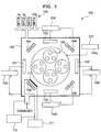
- the multilayer hard film 1 can be preferably formed by a film-formation system 100 illustrated in FIG. 5 .
- the film-formation system 100 is a composite apparatus made by combining the above mentioned vacuum arc vaporization apparatus and sputtering apparatus.
- the film-formation system 100 is provided with a vacuum arc vaporization source 101 equipped with a target material forming a layer A 11, and a sputtering evaporation source 102 equipped with a target material forming a layer B 12, all of which are inside a chamber 103.
- the film-formation system 100 conducts the steps of: rotating the substrate 2 inside the chamber 103, simultaneously making the vacuum arc vaporization source 101 and the sputtering evaporation source 102 discharge electricity at the same timing, thereby alternately stacking the layer A 11 and the layer B 12 one another over the surface of the substrate 2.
- the substrate 2 can be rotated by being on a platform 105 which is rotatable inside the chamber 103.
- the sputtering evaporation source 102 is called an unbalanced magnetron sputtering evaporation source and, for example, UBMS 202 (Kobe Seiko Sho) can be preferably used.
- the film-formation system 100 has a pair of vacuum arc vaporization sources 101 and a pair of sputtering evaporation sources 102.
- the arrangement is not limited to the above example, and it is possible to arrange three sets of the sources 101 and 102 to be alternately located.
- the adhesion between the layer A 11 and the layer B 12 can be increased.
- the discharge of the vacuum arc vaporization sources 101 is terminated.
- the layer B 12 is formed by discharge of the sputtering evaporation source 102.
- This process allows the layers A 11 and B 12 to be alternately stacked. Note the discharge of the vacuum arc vaporization sources 101 and the sputtering evaporation sources 102 may be simultaneously performed when the layer A 11 and the layer B 12 are formed.
- the film-formation system 100 is provided with a vacuum pump (not shown), a gas supply mechanism 104, a platform 105, a heater 106, a bias power supply 107, sputtering power supplies 108, and arc power supplies 109.
- the gas supply mechanism 104 supplies gas such as Ar, N2, or CH 4 to the chamber 103 in the film-formation system 100 corresponding to a film-formation process thus executed.
- Note MFC1 - MFC4 in FIG. 5 are mass flow meters.
- the vacuum pump (not shown) controls a vacuum level inside the chamber 103 at a necessary degree.
- the substrates 2, on which a stack of the layers A 11 and B layers 12 is to be formed, are placed on the platform 105, and then heated by the heaters 106.
- One or more target materials selected from the group of, for example, TiB 2 , SiC and B 4 C are set in one of the sputtering evaporation sources 102 for forming the layer B 12, and the same or the different target materials selected from the above group are set in the other sputtering evaporation source 102.
- a target material for forming the layer A 11 or a target material for forming the underlying layer 13 in the case where the underlying layer 13 is formed is set in the vacuum arc vaporization sources 101.
- a target material selected from any one of Ti 0.8 Si 0.2 , Ti 0.95 Si 0.05 , Ti 0.9 Si 0.1 , Ti 0.7 Si 0.3 , Ti 0.6 Si 0.4 , and Ti 0.7 Si 0.2 B 0.1 is set in one of the arc-ion-plating evaporation sources 101.
- the bias power supply 107 applies a bias voltage to the platform 105, so that the bias voltage is applied to the substrates 2 placed on the platform 105.
- the sputtering power supplies 108 control the potentials of the sputtering evaporation sources 102 so that atoms, ions, or clusters are generated from the sputtering evaporation sources 102.
- the arc power supplies 109 control the potentials of the vacuum arc vaporization sources 101 so that atoms, ions, or clusters are generated from the vacuum arc vaporization sources 101.
- the film-formation system 100 is further provided with a filament-type ion source 110, an AC (Alternating Current) power supply 111 for heating the filament-type ion source 110, and a DC (Direct Current) power supply 112 for discharge of the ion source 110.
- a filament-type ion source 110 for heating the filament-type ion source 110
- a DC (Direct Current) power supply 112 for discharge of the ion source 110.
- C and/or N element can be introduced into the above described layers by decomposition of gas such as N 2 or CH 4 supplied from the gas supply mechanism 104.
- the multilayer hard film 1 is formed on a surface of a substrate 2 of the members included in slide members over which other members are to slide, , for example, jigs, tools, mechanical components such as dies for molding and punches and metal cutting tools each requiring the wear resistance.
- a multilayer hard film 1 is excellent in the adhesion to the substrate 2, the hardness, and the oxidation resistance. Accordingly, the integrated effects of the thickness of the stacked layers A and layers B in the multilayer hard film, the thickness of the multilayer hard film, the composition of the underlying layer combined with the thickness of the underlying layer enable the lifetime of the members 10, 20, 30 and 40 to be elongated.
- Example A various films that are described below were formed on surfaces of substrates.
- Some of the substrates were made of a mirror-finished alloy with ultrahardness (JIS-P series), and other substrates were made of an insert of an ultrahard alloy (ADCT 1505 PDFR-HM grade IC28, ISCAR Ltd.).
- a film formed on the former substrate was used for evaluation of the hardness, and a film formed on the latter substrate was used for evaluation of the tool lifetime.
- the films were formed on the surfaces of the substrates by a film-formation system including a plurality of vacuum arc vaporization sources (having diameters of 100 mm ⁇ ; referred to as "AIP evaporation sources” hereinafter) and a plurality of evaporation sources for sputtering (having diameters of 6 inches ⁇ ; referred to as "SP evaporation sources” hereinafter).
- AIP evaporation sources having diameters of 100 mm ⁇
- SP evaporation sources a plurality of evaporation sources for sputtering
- Target materials for forming the underlying layer and /or target materials for forming the layer A were attached to the AIP evaporation sources of the film-formation system by combining materials shown by the conditions of Nos. A1 - A73 in Tables 1-3.
- target materials for forming the layer B were attached to the SP evaporation sources of the film-formation system by combining materials shown by the conditions of Nos. A1 - A73 in Tables 1-3. Note the AIP evaporation source for forming the layer A and the sputtering evaporation source for forming the layer B were alternately arranged one another so as to form the multilayer hard films.
- the underlying layer and the layers A and B were formed in the conditions of the thicknesses (nm), the number of stacked layers A and B, and the total thickness of the layers A and b thus stacked, as indicated in Tables 4 - 6.
- the mark of "-" in Tables 1 - 3 means that target materials were not attached, and the mark of "-" in Tables 4 - 6 means that no layers were formed.
- the films were formed by the film-formation system having three sputtering evaporation sources under the conditions of Nos. A48, A66, A72 and A73. [Table 1] No.
- the layers in each of the films were formed in the following process.
- a chamber was evacuated to the vacuum of 1 x 10 -3 Pa or lower, and then the substrate was heated to 500°C. Thereafter, Ar (argon) ion sputter cleaning was performed. Then, N 2 gas was introduced into the chamber to set the pressure inside the chamber at 4 Pa.
- Ar argon
- a layer A was formed with a thin thickness via conducting an arc discharge in a short period as rotating substrates placed on the platform.
- a layer B was formed with a thin thickness via conducting a sputtering discharge with the power of 2 kW in a short period.
- the number of pairs of layers A and B and each thickness of the respective layers were controlled, for example, by varying the rotation speed of the substrates from approximately 1 - 10 rpm or varying the electric power inputted into the respective evaporation sources.
- the hardness was measured by using a Vickers hardness tester with the load of 0.25 N.
- the tool lifetimes depend on combination of various factors including: the hardness and the oxidation resistance of each film; the thickness of each film, the overall thickness of the multilayer hard film, the adhesion of the multilayer hard film to the substrate; and the strength of the substrate. Therefore, the tool lifetimes were evaluated by a cutting test. In the cutting test, each of the ultrahard alloy-made inserts with the films was held to an end mill, and then dry-turning of a workpiece material was performed under the following conditions:
- Workpiece Material AISI 316; Cutting Speed: 180 m/min; Feed: 0.14 mm/tooth; Depth of Cut: 4.5 mm; and Lubrication Test: dry.
- Table 7 indicates the results of the hardness test and the cutting test.
- the ultrahard alloy-made insert with a film formed under the condition of No. A1 was used as a reference specimen.
- the tool lifetime of the reference specimen was defined as 100%, and each tool lifetime of the test samples was indicated as a relative value to the tool lifetime of the reference specimen. Accordingly, the data in Table 7 indicate that the higher the relative value becomes, the longer the tool lifetime becomes. [Table 7] No.
- each of the test samples prepared under the conditions of Nos. A7 - A11, A13 - A20, A23, A24, A27, A30, A31, A35, A38, A41, A44, A46 - A66, and A68 - A73 satisfied the criteria of the present invention, thereby to have the higher hardness and longer tool lifetime than the reference specimen, that is, a conventional example made under the condition of No. A1.
- the underlying layer formed on the surface of the substrate under the conditions of Nos. A49 - A66, A68 - A71, and A7 enables the test samples to exhibit highly superior results in the hardness and the tool lifetime.
- A49 - A51, A53, A55 - A71, and A73 are formed of the aforementioned composition M 1-y Al y (B a C b N c O d ), where 0.05 ⁇ y ⁇ 0.8, 0 ⁇ a ⁇ 0.2, 0 ⁇ b ⁇ 0.4, 0.5 ⁇ c ⁇ 1, 0 ⁇ d ⁇ 0.2, and M is one or more selected from Si, Y, the Group 4A elements, the Group 5A elements, and the Group 6A elements of the Periodic Table. Accordingly, this construction led to the superior hardness and elongation of the tool lifetime.
- test samples made under the conditions of Nos. A1 - A6, A12, A21, A22, A25, A26, A28, A29, A32- A34, A36, A37, A39, A40, A42, A43, A45, and A67 do not fulfill at least one of the criteria of the present invention,. This drawback led to the poor hardness and/or tool lifetime.
- test samples made under the conditions of Nos. A2 - A4 included only layers B without forming layers A. Thus, this led to the equal or lower hardness, and shorter tool lifetimes.
- a test sample made under the condition of A12 had layers A in which the atomic ratio of Si was greater than 0.4. Thus, this led to the lower hardness and shorter tool lifetime.
- a test sample made under the condition of A21 had layers A each of which thickness was more than 100 nm. Thus, this led to the lower hardness and shorter tool lifetime.
- a test sample made under the condition of A22 had layers B each of which thickness was less than 2 nm. Thus, this led to the shorter tool lifetime than that made under the condition of A1.
- a test sample made under the condition of A25 had layers B each of which thickness was more than 20 nm. Thus, this led to the lower hardness and shorter tool lifetime.
- a test sample made under the condition of A26 had layers B formed of TiBN in which the atomic ratio of B was less than 0.2, and a test sample made under the condition of A28 had layers B formed of TiBN in which the atomic ratio of B was more than 0.5. Thus, both samples had the lower hardness and shorter tool lifetimes.
- a test sample made under the condition of A29 had layers B formed of TiBN in which the atomic ratio of N was less than 0.25, and a test sample made under the condition of A33 had layers B formed of TiBN in which the atomic ratio of N was more than 0.6. Accordingly, both samples had the lower hardness and shorter tool lifetimes.
- a test sample made under the condition of A32 had layers B formed of TiBCN in which the atomic ratio of C was more than 0.5. Thus, the sample had the lower hardness and shorter tool lifetime.
- a test sample made under the condition of A34 had layers B formed of SiCN in which the atomic ratio of C was less than 0.2, and a test sample made under the condition of A36 had layers B formed of SiCN in which the atomic ratio of C was more than 0.5. Accordingly, both samples had the lower hardness and shorter tool lifetimes.
- a test sample made under the condition of A37 had layers B formed of SiCN in which the atomic ratio of N was less than 0.25, and a test sample made under the condition of A39 had layers B formed of SiCN in which the atomic ratio of N was more than 0.5. Accordingly, both samples had the lower hardness and shorter tool lifetimes.
- a test sample made under the condition of A43 had layers B formed of BCN in which the atomic ratio of N was less than 0.3, and a test sample made under the condition of A45 had layers B formed of BCN in which the atomic ratio of N was more than 0.55. Accordingly, both samples had the lower hardness and shorter tool lifetimes.
- a test sample made under the condition of A67 had layers A and B of which total thickness was less than 500 nm. Accordingly, this led to the lower shorter tool lifetime.
- Example B various films were formed on surfaces of substrates as explained hereinafter.
- substrates used were a mirror-finished substrate made of an ultrahard alloy (JIS-P type), and an ultrahard alloy-made insert (ISCAR Ltd., ADCT 1505 PDFR-HM grade IC28).
- the films formed on the former substrate was used for evaluation of the adhesion strength, and the films formed on the latter substrate were used for evaluation of the tool lifetime.
- a film-formation system containing a plurality of AIP evaporation sources and a plurality of SP evaporation sources was used in the formation of films on the surface of the substrates as in Example A.
- target materials for forming the underlying layers and/or layers A under the conditions Nos. B1 - B60 shown in Tables 8 and 9 were attached to the AIP evaporation sources in the film-formation system. Further, target materials for forming layers B under the conditions of Nos. B1 - B60 in Tables 8 and 9 were attached to the SP evaporation sources in the film-formation system.
- the above mentioned layers were formed in the following method.
- the method included the steps of: introducing a cleaned substrate into the film-formation system; reducing the pressure inside a chamber to be 1 x 10 -3 Pa or lower, and heating the substrate up to 500°C. Thereafter, the method further included the additional steps of: conducting the sputter cleaning in use of Ar (argon) ion; and introducing N 2 gas into the chamber so as to adjust the pressure inside the chamber to be 4Pa.
- Ar argon
- the layers A and B were formed with or without forming the underlying layer as shown in Tables 10 and 11.
- the underlying layer and each of the layers A were formed by conducting an arc discharge with the current of 150 A under N 2 atmosphere (Note a small amount of CH 4 gas was additionally introduced under the conditions of Nos. B14 and B15).
- a layer A was formed, the arc discharge was stopped. Then, a layer B was formed by reducing the pressure to 0.6 Pa with introducing Ar gas into the chamber, and conducting a sputtering process. Thus a pair of layers A and B is formed. The formation of the pairs of layers A and B were repeatedly conducted in this order.
- the adhesion performance of the test samples were evaluated by ultrahard alloy-made substrates with films formed under the conditions of Nos. B1-B60. Further, the lifetimes as a tool (or tool lifetimes) of the test samples were evaluated by ultrahard alloy-made inserts with films formed under the conditions of Nos. B1-B60.
- the adhesion was evaluated by a scratch test. Each scratch test was conducted by sliding a diamond indenter having a tip radius of 200 ⁇ mR was slid on the ultrahard hard alloy-made substrate having the film under the conditions of a load increasing rate of 100 N/min, and a moving speed of 10 mm/min.
- tool lifetimes are influenced by combination of various factors including the hardness and the oxidation resistance of each film, the thickness of each film, the overall thickness of the multilayer hard film, the adhesion property of the multilayer hard film to the substrate, and the strength of the substrate. Therefore, the tool lifetime was evaluated by a cutting test. Each cutting test was conducted by the steps of: fixing an ultrahard alloy-made insert with a film to an end mill, and dry-turning a workpiece material under the following conditions:
- Workpiece Material AISI 316; Cutting Speed: 200 m/min; Feed: 0.14 mm/tooth; Depth of Cut: 4.5 mm; and Lubrication Test dry.
- Table 12 indicates the results of evaluation of the adhesion and the total lifetime of the test samples. Note in the Table 12, an ultrahard alloy-made insert with a film formed under the conditions of No. B1 is used as a reference specimen. The lifetime of the reference specimen is defined as 100%, and a lifetime of each test sample is shown in a percentage relative to the lifetime of the reference specimen. Herein, the data in the table indicate that the higher the percentage becomes, the longer the lifetime becomes. [Table 12] No.
- test samples prepared under the conditions of Nos B7 - B11, B13 - B15, B17, B19, B21 - B25, B27 - B57, B59 and B60 satisfied the criteria of the present invention. Accordingly, the above listed test samples had higher adhesion (that is, excellent in the adhesion property) between the substrate and the film (or multilayer hard film) and longer tool lifetimes than those of the reference specimen having no layers A and B (that is, conventional example) made under the conditions of No. B1.
- the underlying layers were formed of M 1-y Al y (B a C b N c O d ), where 0.05 ⁇ y ⁇ 0.8, 0 ⁇ a ⁇ 0.2, 0 ⁇ b ⁇ 0.4, 0.5 ⁇ c ⁇ 1, 0 ⁇ d ⁇ 0.2, and M was one or more selected from Si, Y, the Group 4A elements, the Group 5A elements, and the Group 6A elements, under the conditions of Nos. B33 - B35, B37, and B39 - B55. That construction led to the further superior results in the adhesion and tool lifetimes.
- test samples made under the conditions of Nos. B1 - B6, B12, B16, B18, B20, B26 and B58 did not fulfill at least one of the criteria of the present invention. Consequently, this resulted in the lower adhesion and/or shorter lifetimes of the above listed test samples than those of the reference specimen made under the conditions of No. B1.
- test samples had lower adhesion and shorter tool lifetimes than the reference specimen made under the conditions of No. B1.
- test sample made under conditions of B5 was prepared without forming a layer A, which resulted in the lower adhesion and shorter tool lifetime thereof than those of the reference specimen made under the conditions of No. B1.
- test sample made under conditions of No.B12 had layers A containing Si at the atomic ratio greater than 0.4, which resulted in the shorter tool lifetime thereof than that of the reference specimen made under the conditions of No. B1.
- the test sample made under conditions of No.B16 had layers A each having a thickness less than 100 nm, which resulted in the lower adhesion and shorter tool lifetime thereof than those of the reference specimen made under the conditions of No. B1.
- the test sample made under conditions of No.B18 had layers B each having a thickness less than 50 nm, which resulted in the lower adhesion and shorter tool lifetime thereof than those of the reference specimen made under the conditions of No. B1.
- the test sample made under conditions of No.B20 had layers A and B having a total thickness less than 500 nm, which resulted in the lower adhesion and shorter tool lifetime of thereof than those of the reference specimen made under the conditions of No. B1.
- the test sample made under conditions of No.B26 was formed with a film by replacing the layer A with the layer B. That is, the SiC layer was formed at the position of the layer A ,and Ti 0.6 Si 0.2 N layer was formed at the position of the layer B. That construction resulted in the lower adhesion and shorter tool lifetime thereof than those of the reference specimen made under the conditions of No. B1.
- test sample made under conditions of No.B58 had layers B containing more amount of N, which resulted in the lower adhesion and shorter tool lifetime of thereof than those of the reference specimen made under the conditions of No. B1
Landscapes
- Chemical & Material Sciences (AREA)
- Engineering & Computer Science (AREA)
- Organic Chemistry (AREA)
- Materials Engineering (AREA)
- Mechanical Engineering (AREA)
- Metallurgy (AREA)
- Chemical Kinetics & Catalysis (AREA)
- Inorganic Chemistry (AREA)
- Ceramic Engineering (AREA)
- Physical Vapour Deposition (AREA)
- Cutting Tools, Boring Holders, And Turrets (AREA)
- Drilling Tools (AREA)
- Laminated Bodies (AREA)
Applications Claiming Priority (3)
| Application Number | Priority Date | Filing Date | Title |
|---|---|---|---|
| JP2011274956A JP5681093B2 (ja) | 2011-12-15 | 2011-12-15 | 多層硬質皮膜 |
| JP2011274960A JP5681094B2 (ja) | 2011-12-15 | 2011-12-15 | 積層硬質皮膜 |
| PCT/JP2012/082575 WO2013089254A1 (ja) | 2011-12-15 | 2012-12-14 | 多層硬質皮膜およびその製造方法 |
Publications (3)
| Publication Number | Publication Date |
|---|---|
| EP2792765A1 EP2792765A1 (en) | 2014-10-22 |
| EP2792765A4 EP2792765A4 (en) | 2015-11-11 |
| EP2792765B1 true EP2792765B1 (en) | 2018-09-12 |
Family
ID=48612693
Family Applications (1)
| Application Number | Title | Priority Date | Filing Date |
|---|---|---|---|
| EP12857851.5A Not-in-force EP2792765B1 (en) | 2011-12-15 | 2012-12-14 | Multilayer hard film and method for producing same |
Country Status (7)
| Country | Link |
|---|---|
| US (1) | US9340863B2 (enExample) |
| EP (1) | EP2792765B1 (enExample) |
| KR (1) | KR101625774B1 (enExample) |
| CN (1) | CN104126025B (enExample) |
| IL (1) | IL233105B (enExample) |
| IN (1) | IN2014CN04404A (enExample) |
| WO (1) | WO2013089254A1 (enExample) |
Families Citing this family (8)
| Publication number | Priority date | Publication date | Assignee | Title |
|---|---|---|---|---|
| JP6131145B2 (ja) | 2013-08-06 | 2017-05-17 | 株式会社神戸製鋼所 | 成膜装置 |
| DE102013019691A1 (de) * | 2013-11-26 | 2015-05-28 | Oerlikon Trading Ag, Trübbach | Hartstoffschicht zur Reduzierung eines Wärmeeintrags in das beschichtete Substrat |
| JP6163141B2 (ja) * | 2014-07-01 | 2017-07-12 | 株式会社神戸製鋼所 | 硬質皮膜 |
| RU2631572C1 (ru) * | 2016-04-11 | 2017-09-25 | Общество с ограниченной ответственностью "Научно-производственное предприятие "Уралавиаспецтехнология" | Способ нанесения многослойного ионно-плазменного покрытия на поверхность гравюры штампа из жаропрочной стали |
| JP6934772B2 (ja) * | 2017-08-21 | 2021-09-15 | シチズン時計株式会社 | 黒色部材、黒色部材の製造方法および黒色部材を含む時計 |
| GB201802468D0 (en) | 2018-02-15 | 2018-04-04 | Rolls Royce Plc | Coated substrate |
| CN109023263A (zh) * | 2018-08-03 | 2018-12-18 | 河北工程大学 | TiAl/TiAlN/TiCrAlN复合涂层及其制备方法 |
| CN110857465B (zh) * | 2018-08-22 | 2021-11-19 | 赣州澳克泰工具技术有限公司 | 刀具及其制造方法 |
Family Cites Families (24)
| Publication number | Priority date | Publication date | Assignee | Title |
|---|---|---|---|---|
| JPH04184691A (ja) | 1990-11-20 | 1992-07-01 | Nec Corp | シングルチップマイクロコンピュータ |
| JP3914687B2 (ja) | 2000-04-11 | 2007-05-16 | 住友電工ハードメタル株式会社 | 切削工具とその製造方法 |
| SE522722C2 (sv) | 2001-03-28 | 2004-03-02 | Seco Tools Ab | Skärverktyg belagt med titandiborid |
| CN100419117C (zh) * | 2004-02-02 | 2008-09-17 | 株式会社神户制钢所 | 硬质叠层被膜、其制造方法及成膜装置 |
| US7758950B2 (en) * | 2004-07-23 | 2010-07-20 | Sumitomo Electric Hardmetal Corp. | Surface-coated cutting tool with coated film having strength distribution of compressive stress |
| SE0402180D0 (sv) | 2004-09-10 | 2004-09-10 | Sandvik Ab | Deposition of Ti1-xAlxN using Bipolar Pulsed Dual Magnetron Sputtering |
| US7348074B2 (en) | 2005-04-01 | 2008-03-25 | Oc Oerlikon Balzers Ag | Multilayer hard coating for tools |
| JP4817044B2 (ja) | 2005-09-28 | 2011-11-16 | 住友金属工業株式会社 | 切削工具の製造方法 |
| JP4380622B2 (ja) * | 2005-11-04 | 2009-12-09 | 日立ツール株式会社 | 多層皮膜被覆部材及びその製造方法 |
| EP2256229A1 (de) * | 2005-11-04 | 2010-12-01 | Sulzer Metaplas GmbH | Schichtsystem zur Bildung einer Oberflächenschicht auf einer Oberfläche eines Substrats, Beschichtungsverfahren und Substrat mit einem Schichtsystem |
| JP4883475B2 (ja) | 2005-11-08 | 2012-02-22 | 三菱マテリアル株式会社 | 高硬度鋼の高速切削加工で硬質被覆層がすぐれた耐摩耗性を発揮する表面被覆立方晶窒化ほう素基超高圧焼結材料製切削工具 |
| JP4883473B2 (ja) * | 2005-11-08 | 2012-02-22 | 三菱マテリアル株式会社 | 高硬度鋼の重切削加工で硬質被覆層がすぐれた耐チッピング性を発揮する表面被覆立方晶窒化ほう素基超高圧焼結材料製切削工具 |
| JP4699978B2 (ja) * | 2006-08-09 | 2011-06-15 | 株式会社神戸製鋼所 | 硬質皮膜被覆材 |
| CN100558552C (zh) | 2006-08-09 | 2009-11-11 | 株式会社神户制钢所 | 硬质皮膜及硬质皮膜被覆材 |
| US8507110B2 (en) * | 2008-04-18 | 2013-08-13 | Sandvik Intellectual Property Ab | Coated cutting tool and a method of making thereof |
| WO2009133814A1 (ja) * | 2008-04-30 | 2009-11-05 | 住友電気工業株式会社 | 表面被覆切削工具 |
| JP4900839B2 (ja) * | 2008-07-31 | 2012-03-21 | 日立ツール株式会社 | 多層皮膜被覆部材及びその製造方法 |
| EP2149624B1 (en) * | 2008-07-31 | 2012-08-08 | Sulzer Metaplas GmbH | Multilayer film-coated member and method for producing it |
| EP2149620B1 (en) * | 2008-07-31 | 2020-04-29 | Oerlikon Surface Solutions AG, Pfäffikon | Multilayer film-coated member and method for producing it |
| JP5246596B2 (ja) | 2009-03-06 | 2013-07-24 | 三菱マテリアル株式会社 | 表面被覆立方晶窒化ほう素基超高圧焼結材料製切削工具 |
| JP5156971B2 (ja) * | 2009-03-17 | 2013-03-06 | Smc株式会社 | 溶損防止用被覆部材 |
| JP5293330B2 (ja) | 2009-03-26 | 2013-09-18 | 三菱マテリアル株式会社 | 表面被覆立方晶窒化ほう素基超高圧焼結材料製切削工具 |
| JP5667176B2 (ja) * | 2009-06-18 | 2015-02-12 | スルザー メタプラス ゲーエムベーハー | 保護コーティング、保護コーティングを有するコーティング部材、並びに保護コーティングを製造するための方法 |
| CN102758188A (zh) * | 2011-04-28 | 2012-10-31 | 鸿富锦精密工业(深圳)有限公司 | 镀膜件及其制造方法 |
-
2012
- 2012-12-14 CN CN201280061985.8A patent/CN104126025B/zh not_active Expired - Fee Related
- 2012-12-14 KR KR1020147015483A patent/KR101625774B1/ko not_active Expired - Fee Related
- 2012-12-14 WO PCT/JP2012/082575 patent/WO2013089254A1/ja not_active Ceased
- 2012-12-14 US US14/365,436 patent/US9340863B2/en not_active Expired - Fee Related
- 2012-12-14 EP EP12857851.5A patent/EP2792765B1/en not_active Not-in-force
- 2012-12-14 IN IN4404CHN2014 patent/IN2014CN04404A/en unknown
-
2014
- 2014-06-12 IL IL233105A patent/IL233105B/en active IP Right Grant
Non-Patent Citations (1)
| Title |
|---|
| None * |
Also Published As
| Publication number | Publication date |
|---|---|
| KR20140090667A (ko) | 2014-07-17 |
| KR101625774B1 (ko) | 2016-05-30 |
| EP2792765A1 (en) | 2014-10-22 |
| US9340863B2 (en) | 2016-05-17 |
| IL233105B (en) | 2018-10-31 |
| US20140363648A1 (en) | 2014-12-11 |
| CN104126025A (zh) | 2014-10-29 |
| EP2792765A4 (en) | 2015-11-11 |
| IL233105A0 (en) | 2014-07-31 |
| IN2014CN04404A (enExample) | 2015-09-04 |
| CN104126025B (zh) | 2016-08-24 |
| WO2013089254A1 (ja) | 2013-06-20 |
Similar Documents
| Publication | Publication Date | Title |
|---|---|---|
| US9340863B2 (en) | Multilayer hard film and method for producing same | |
| CA2880949C (en) | Coated tool | |
| US10640864B2 (en) | Coated tool | |
| JP6705565B2 (ja) | 被覆切削工具 | |
| US10265775B2 (en) | Coated tool | |
| EP3173169B1 (en) | Coated cutting tool | |
| TWI658161B (zh) | 硬質被膜及硬質被膜被覆構件 | |
| US8460803B2 (en) | Hard coating layer and method for forming the same | |
| EP2336383A1 (en) | Multilayered coated cutting tool | |
| US20180347027A1 (en) | Multilayer nitride hard coatings | |
| EP3763465B1 (en) | Surface-coated cutting tool and method for producing same | |
| EP3763466B1 (en) | Surface-coated cutting tool and method for producing same | |
| EP2060655A1 (en) | Hard coating and method for forming hard coating | |
| CN100509224C (zh) | 具有压缩应力的强度分布的有涂膜的表面涂敷切削工具 | |
| EP3109341A1 (en) | Hard coating film and method of forming same | |
| JP5681093B2 (ja) | 多層硬質皮膜 | |
| JP2017505856A (ja) | コートされた基材への入熱を減少させるための硬質材料層 | |
| JP5681094B2 (ja) | 積層硬質皮膜 | |
| CN103339283B (zh) | 硬质层叠被膜 | |
| CN103339284B (zh) | 硬质层叠被膜 | |
| CN100446901C (zh) | 具有压缩应力的强度分布的有涂膜的表面涂敷切削工具 | |
| EP3330402A1 (en) | Hard coating and hard coating-covered member |
Legal Events
| Date | Code | Title | Description |
|---|---|---|---|
| PUAI | Public reference made under article 153(3) epc to a published international application that has entered the european phase |
Free format text: ORIGINAL CODE: 0009012 |
|
| 17P | Request for examination filed |
Effective date: 20140618 |
|
| AK | Designated contracting states |
Kind code of ref document: A1 Designated state(s): AL AT BE BG CH CY CZ DE DK EE ES FI FR GB GR HR HU IE IS IT LI LT LU LV MC MK MT NL NO PL PT RO RS SE SI SK SM TR |
|
| DAX | Request for extension of the european patent (deleted) | ||
| RA4 | Supplementary search report drawn up and despatched (corrected) |
Effective date: 20151012 |
|
| RIC1 | Information provided on ipc code assigned before grant |
Ipc: B23B 27/14 20060101ALI20151006BHEP Ipc: C23C 28/04 20060101ALI20151006BHEP Ipc: C23C 14/06 20060101AFI20151006BHEP Ipc: B23C 5/16 20060101ALI20151006BHEP |
|
| RIC1 | Information provided on ipc code assigned before grant |
Ipc: C23C 28/00 20060101ALI20180125BHEP Ipc: B23C 5/16 20060101ALI20180125BHEP Ipc: B23B 27/14 20060101ALI20180125BHEP Ipc: C23C 28/04 20060101ALI20180125BHEP Ipc: C23C 14/06 20060101AFI20180125BHEP |
|
| GRAJ | Information related to disapproval of communication of intention to grant by the applicant or resumption of examination proceedings by the epo deleted |
Free format text: ORIGINAL CODE: EPIDOSDIGR1 |
|
| GRAP | Despatch of communication of intention to grant a patent |
Free format text: ORIGINAL CODE: EPIDOSNIGR1 |
|
| INTG | Intention to grant announced |
Effective date: 20180328 |
|
| GRAS | Grant fee paid |
Free format text: ORIGINAL CODE: EPIDOSNIGR3 |
|
| GRAA | (expected) grant |
Free format text: ORIGINAL CODE: 0009210 |
|
| AK | Designated contracting states |
Kind code of ref document: B1 Designated state(s): AL AT BE BG CH CY CZ DE DK EE ES FI FR GB GR HR HU IE IS IT LI LT LU LV MC MK MT NL NO PL PT RO RS SE SI SK SM TR |
|
| REG | Reference to a national code |
Ref country code: GB Ref legal event code: FG4D |
|
| REG | Reference to a national code |
Ref country code: CH Ref legal event code: EP |
|
| REG | Reference to a national code |
Ref country code: IE Ref legal event code: FG4D |
|
| REG | Reference to a national code |
Ref country code: DE Ref legal event code: R096 Ref document number: 602012051118 Country of ref document: DE |
|
| REG | Reference to a national code |
Ref country code: AT Ref legal event code: REF Ref document number: 1040681 Country of ref document: AT Kind code of ref document: T Effective date: 20181015 |
|
| REG | Reference to a national code |
Ref country code: NL Ref legal event code: MP Effective date: 20180912 |
|
| REG | Reference to a national code |
Ref country code: LT Ref legal event code: MG4D |
|
| PG25 | Lapsed in a contracting state [announced via postgrant information from national office to epo] |
Ref country code: GR Free format text: LAPSE BECAUSE OF FAILURE TO SUBMIT A TRANSLATION OF THE DESCRIPTION OR TO PAY THE FEE WITHIN THE PRESCRIBED TIME-LIMIT Effective date: 20181213 Ref country code: BG Free format text: LAPSE BECAUSE OF FAILURE TO SUBMIT A TRANSLATION OF THE DESCRIPTION OR TO PAY THE FEE WITHIN THE PRESCRIBED TIME-LIMIT Effective date: 20181212 Ref country code: NO Free format text: LAPSE BECAUSE OF FAILURE TO SUBMIT A TRANSLATION OF THE DESCRIPTION OR TO PAY THE FEE WITHIN THE PRESCRIBED TIME-LIMIT Effective date: 20181212 Ref country code: LT Free format text: LAPSE BECAUSE OF FAILURE TO SUBMIT A TRANSLATION OF THE DESCRIPTION OR TO PAY THE FEE WITHIN THE PRESCRIBED TIME-LIMIT Effective date: 20180912 Ref country code: RS Free format text: LAPSE BECAUSE OF FAILURE TO SUBMIT A TRANSLATION OF THE DESCRIPTION OR TO PAY THE FEE WITHIN THE PRESCRIBED TIME-LIMIT Effective date: 20180912 Ref country code: FI Free format text: LAPSE BECAUSE OF FAILURE TO SUBMIT A TRANSLATION OF THE DESCRIPTION OR TO PAY THE FEE WITHIN THE PRESCRIBED TIME-LIMIT Effective date: 20180912 Ref country code: SE Free format text: LAPSE BECAUSE OF FAILURE TO SUBMIT A TRANSLATION OF THE DESCRIPTION OR TO PAY THE FEE WITHIN THE PRESCRIBED TIME-LIMIT Effective date: 20180912 |
|
| PG25 | Lapsed in a contracting state [announced via postgrant information from national office to epo] |
Ref country code: AL Free format text: LAPSE BECAUSE OF FAILURE TO SUBMIT A TRANSLATION OF THE DESCRIPTION OR TO PAY THE FEE WITHIN THE PRESCRIBED TIME-LIMIT Effective date: 20180912 Ref country code: LV Free format text: LAPSE BECAUSE OF FAILURE TO SUBMIT A TRANSLATION OF THE DESCRIPTION OR TO PAY THE FEE WITHIN THE PRESCRIBED TIME-LIMIT Effective date: 20180912 Ref country code: HR Free format text: LAPSE BECAUSE OF FAILURE TO SUBMIT A TRANSLATION OF THE DESCRIPTION OR TO PAY THE FEE WITHIN THE PRESCRIBED TIME-LIMIT Effective date: 20180912 |
|
| REG | Reference to a national code |
Ref country code: AT Ref legal event code: MK05 Ref document number: 1040681 Country of ref document: AT Kind code of ref document: T Effective date: 20180912 |
|
| PG25 | Lapsed in a contracting state [announced via postgrant information from national office to epo] |
Ref country code: PL Free format text: LAPSE BECAUSE OF FAILURE TO SUBMIT A TRANSLATION OF THE DESCRIPTION OR TO PAY THE FEE WITHIN THE PRESCRIBED TIME-LIMIT Effective date: 20180912 Ref country code: EE Free format text: LAPSE BECAUSE OF FAILURE TO SUBMIT A TRANSLATION OF THE DESCRIPTION OR TO PAY THE FEE WITHIN THE PRESCRIBED TIME-LIMIT Effective date: 20180912 Ref country code: IS Free format text: LAPSE BECAUSE OF FAILURE TO SUBMIT A TRANSLATION OF THE DESCRIPTION OR TO PAY THE FEE WITHIN THE PRESCRIBED TIME-LIMIT Effective date: 20190112 Ref country code: CZ Free format text: LAPSE BECAUSE OF FAILURE TO SUBMIT A TRANSLATION OF THE DESCRIPTION OR TO PAY THE FEE WITHIN THE PRESCRIBED TIME-LIMIT Effective date: 20180912 Ref country code: ES Free format text: LAPSE BECAUSE OF FAILURE TO SUBMIT A TRANSLATION OF THE DESCRIPTION OR TO PAY THE FEE WITHIN THE PRESCRIBED TIME-LIMIT Effective date: 20180912 Ref country code: IT Free format text: LAPSE BECAUSE OF FAILURE TO SUBMIT A TRANSLATION OF THE DESCRIPTION OR TO PAY THE FEE WITHIN THE PRESCRIBED TIME-LIMIT Effective date: 20180912 Ref country code: RO Free format text: LAPSE BECAUSE OF FAILURE TO SUBMIT A TRANSLATION OF THE DESCRIPTION OR TO PAY THE FEE WITHIN THE PRESCRIBED TIME-LIMIT Effective date: 20180912 Ref country code: NL Free format text: LAPSE BECAUSE OF FAILURE TO SUBMIT A TRANSLATION OF THE DESCRIPTION OR TO PAY THE FEE WITHIN THE PRESCRIBED TIME-LIMIT Effective date: 20180912 Ref country code: AT Free format text: LAPSE BECAUSE OF FAILURE TO SUBMIT A TRANSLATION OF THE DESCRIPTION OR TO PAY THE FEE WITHIN THE PRESCRIBED TIME-LIMIT Effective date: 20180912 |
|
| PGFP | Annual fee paid to national office [announced via postgrant information from national office to epo] |
Ref country code: DE Payment date: 20181218 Year of fee payment: 7 |
|
| PG25 | Lapsed in a contracting state [announced via postgrant information from national office to epo] |
Ref country code: SK Free format text: LAPSE BECAUSE OF FAILURE TO SUBMIT A TRANSLATION OF THE DESCRIPTION OR TO PAY THE FEE WITHIN THE PRESCRIBED TIME-LIMIT Effective date: 20180912 Ref country code: SM Free format text: LAPSE BECAUSE OF FAILURE TO SUBMIT A TRANSLATION OF THE DESCRIPTION OR TO PAY THE FEE WITHIN THE PRESCRIBED TIME-LIMIT Effective date: 20180912 Ref country code: PT Free format text: LAPSE BECAUSE OF FAILURE TO SUBMIT A TRANSLATION OF THE DESCRIPTION OR TO PAY THE FEE WITHIN THE PRESCRIBED TIME-LIMIT Effective date: 20190112 |
|
| REG | Reference to a national code |
Ref country code: DE Ref legal event code: R097 Ref document number: 602012051118 Country of ref document: DE |
|
| PLBE | No opposition filed within time limit |
Free format text: ORIGINAL CODE: 0009261 |
|
| STAA | Information on the status of an ep patent application or granted ep patent |
Free format text: STATUS: NO OPPOSITION FILED WITHIN TIME LIMIT |
|
| PG25 | Lapsed in a contracting state [announced via postgrant information from national office to epo] |
Ref country code: DK Free format text: LAPSE BECAUSE OF FAILURE TO SUBMIT A TRANSLATION OF THE DESCRIPTION OR TO PAY THE FEE WITHIN THE PRESCRIBED TIME-LIMIT Effective date: 20180912 |
|
| REG | Reference to a national code |
Ref country code: CH Ref legal event code: PL |
|
| 26N | No opposition filed |
Effective date: 20190613 |
|
| GBPC | Gb: european patent ceased through non-payment of renewal fee |
Effective date: 20181214 |
|
| PG25 | Lapsed in a contracting state [announced via postgrant information from national office to epo] |
Ref country code: SI Free format text: LAPSE BECAUSE OF FAILURE TO SUBMIT A TRANSLATION OF THE DESCRIPTION OR TO PAY THE FEE WITHIN THE PRESCRIBED TIME-LIMIT Effective date: 20180912 Ref country code: LU Free format text: LAPSE BECAUSE OF NON-PAYMENT OF DUE FEES Effective date: 20181214 Ref country code: MC Free format text: LAPSE BECAUSE OF FAILURE TO SUBMIT A TRANSLATION OF THE DESCRIPTION OR TO PAY THE FEE WITHIN THE PRESCRIBED TIME-LIMIT Effective date: 20180912 |
|
| REG | Reference to a national code |
Ref country code: IE Ref legal event code: MM4A |
|
| REG | Reference to a national code |
Ref country code: BE Ref legal event code: MM Effective date: 20181231 |
|
| PG25 | Lapsed in a contracting state [announced via postgrant information from national office to epo] |
Ref country code: IE Free format text: LAPSE BECAUSE OF NON-PAYMENT OF DUE FEES Effective date: 20181214 Ref country code: FR Free format text: LAPSE BECAUSE OF NON-PAYMENT OF DUE FEES Effective date: 20181231 |
|
| PG25 | Lapsed in a contracting state [announced via postgrant information from national office to epo] |
Ref country code: BE Free format text: LAPSE BECAUSE OF NON-PAYMENT OF DUE FEES Effective date: 20181231 |
|
| PG25 | Lapsed in a contracting state [announced via postgrant information from national office to epo] |
Ref country code: GB Free format text: LAPSE BECAUSE OF NON-PAYMENT OF DUE FEES Effective date: 20181214 Ref country code: CH Free format text: LAPSE BECAUSE OF NON-PAYMENT OF DUE FEES Effective date: 20181231 Ref country code: LI Free format text: LAPSE BECAUSE OF NON-PAYMENT OF DUE FEES Effective date: 20181231 |
|
| PG25 | Lapsed in a contracting state [announced via postgrant information from national office to epo] |
Ref country code: MT Free format text: LAPSE BECAUSE OF NON-PAYMENT OF DUE FEES Effective date: 20181214 |
|
| PG25 | Lapsed in a contracting state [announced via postgrant information from national office to epo] |
Ref country code: TR Free format text: LAPSE BECAUSE OF FAILURE TO SUBMIT A TRANSLATION OF THE DESCRIPTION OR TO PAY THE FEE WITHIN THE PRESCRIBED TIME-LIMIT Effective date: 20180912 |
|
| PG25 | Lapsed in a contracting state [announced via postgrant information from national office to epo] |
Ref country code: CY Free format text: LAPSE BECAUSE OF FAILURE TO SUBMIT A TRANSLATION OF THE DESCRIPTION OR TO PAY THE FEE WITHIN THE PRESCRIBED TIME-LIMIT Effective date: 20180912 Ref country code: MK Free format text: LAPSE BECAUSE OF NON-PAYMENT OF DUE FEES Effective date: 20180912 Ref country code: HU Free format text: LAPSE BECAUSE OF FAILURE TO SUBMIT A TRANSLATION OF THE DESCRIPTION OR TO PAY THE FEE WITHIN THE PRESCRIBED TIME-LIMIT; INVALID AB INITIO Effective date: 20121214 |
|
| REG | Reference to a national code |
Ref country code: DE Ref legal event code: R119 Ref document number: 602012051118 Country of ref document: DE |
|
| PG25 | Lapsed in a contracting state [announced via postgrant information from national office to epo] |
Ref country code: DE Free format text: LAPSE BECAUSE OF NON-PAYMENT OF DUE FEES Effective date: 20200701 |