WO2013080770A1 - 液晶表示装置及びその駆動方法 - Google Patents
液晶表示装置及びその駆動方法 Download PDFInfo
- Publication number
- WO2013080770A1 WO2013080770A1 PCT/JP2012/078989 JP2012078989W WO2013080770A1 WO 2013080770 A1 WO2013080770 A1 WO 2013080770A1 JP 2012078989 W JP2012078989 W JP 2012078989W WO 2013080770 A1 WO2013080770 A1 WO 2013080770A1
- Authority
- WO
- WIPO (PCT)
- Prior art keywords
- data
- unit
- subframe
- pixel
- liquid crystal
- Prior art date
- Legal status (The legal status is an assumption and is not a legal conclusion. Google has not performed a legal analysis and makes no representation as to the accuracy of the status listed.)
- Ceased
Links
Images


Classifications
-
- G—PHYSICS
- G09—EDUCATION; CRYPTOGRAPHY; DISPLAY; ADVERTISING; SEALS
- G09G—ARRANGEMENTS OR CIRCUITS FOR CONTROL OF INDICATING DEVICES USING STATIC MEANS TO PRESENT VARIABLE INFORMATION
- G09G3/00—Control arrangements or circuits, of interest only in connection with visual indicators other than cathode-ray tubes
- G09G3/20—Control arrangements or circuits, of interest only in connection with visual indicators other than cathode-ray tubes for presentation of an assembly of a number of characters, e.g. a page, by composing the assembly by combination of individual elements arranged in a matrix no fixed position being assigned to or needed to be assigned to the individual characters or partial characters
- G09G3/34—Control arrangements or circuits, of interest only in connection with visual indicators other than cathode-ray tubes for presentation of an assembly of a number of characters, e.g. a page, by composing the assembly by combination of individual elements arranged in a matrix no fixed position being assigned to or needed to be assigned to the individual characters or partial characters by control of light from an independent source
- G09G3/36—Control arrangements or circuits, of interest only in connection with visual indicators other than cathode-ray tubes for presentation of an assembly of a number of characters, e.g. a page, by composing the assembly by combination of individual elements arranged in a matrix no fixed position being assigned to or needed to be assigned to the individual characters or partial characters by control of light from an independent source using liquid crystals
- G09G3/3611—Control of matrices with row and column drivers
- G09G3/3648—Control of matrices with row and column drivers using an active matrix
-
- G—PHYSICS
- G02—OPTICS
- G02F—OPTICAL DEVICES OR ARRANGEMENTS FOR THE CONTROL OF LIGHT BY MODIFICATION OF THE OPTICAL PROPERTIES OF THE MEDIA OF THE ELEMENTS INVOLVED THEREIN; NON-LINEAR OPTICS; FREQUENCY-CHANGING OF LIGHT; OPTICAL LOGIC ELEMENTS; OPTICAL ANALOGUE/DIGITAL CONVERTERS
- G02F1/00—Devices or arrangements for the control of the intensity, colour, phase, polarisation or direction of light arriving from an independent light source, e.g. switching, gating or modulating; Non-linear optics
- G02F1/01—Devices or arrangements for the control of the intensity, colour, phase, polarisation or direction of light arriving from an independent light source, e.g. switching, gating or modulating; Non-linear optics for the control of the intensity, phase, polarisation or colour
- G02F1/13—Devices or arrangements for the control of the intensity, colour, phase, polarisation or direction of light arriving from an independent light source, e.g. switching, gating or modulating; Non-linear optics for the control of the intensity, phase, polarisation or colour based on liquid crystals, e.g. single liquid crystal display cells
- G02F1/133—Constructional arrangements; Operation of liquid crystal cells; Circuit arrangements
-
- G—PHYSICS
- G09—EDUCATION; CRYPTOGRAPHY; DISPLAY; ADVERTISING; SEALS
- G09G—ARRANGEMENTS OR CIRCUITS FOR CONTROL OF INDICATING DEVICES USING STATIC MEANS TO PRESENT VARIABLE INFORMATION
- G09G3/00—Control arrangements or circuits, of interest only in connection with visual indicators other than cathode-ray tubes
- G09G3/20—Control arrangements or circuits, of interest only in connection with visual indicators other than cathode-ray tubes for presentation of an assembly of a number of characters, e.g. a page, by composing the assembly by combination of individual elements arranged in a matrix no fixed position being assigned to or needed to be assigned to the individual characters or partial characters
- G09G3/2007—Display of intermediate tones
- G09G3/2018—Display of intermediate tones by time modulation using two or more time intervals
- G09G3/2022—Display of intermediate tones by time modulation using two or more time intervals using sub-frames
-
- G—PHYSICS
- G09—EDUCATION; CRYPTOGRAPHY; DISPLAY; ADVERTISING; SEALS
- G09G—ARRANGEMENTS OR CIRCUITS FOR CONTROL OF INDICATING DEVICES USING STATIC MEANS TO PRESENT VARIABLE INFORMATION
- G09G3/00—Control arrangements or circuits, of interest only in connection with visual indicators other than cathode-ray tubes
- G09G3/20—Control arrangements or circuits, of interest only in connection with visual indicators other than cathode-ray tubes for presentation of an assembly of a number of characters, e.g. a page, by composing the assembly by combination of individual elements arranged in a matrix no fixed position being assigned to or needed to be assigned to the individual characters or partial characters
- G09G3/2007—Display of intermediate tones
- G09G3/2059—Display of intermediate tones using error diffusion
-
- G—PHYSICS
- G09—EDUCATION; CRYPTOGRAPHY; DISPLAY; ADVERTISING; SEALS
- G09G—ARRANGEMENTS OR CIRCUITS FOR CONTROL OF INDICATING DEVICES USING STATIC MEANS TO PRESENT VARIABLE INFORMATION
- G09G2300/00—Aspects of the constitution of display devices
- G09G2300/08—Active matrix structure, i.e. with use of active elements, inclusive of non-linear two terminal elements, in the pixels together with light emitting or modulating elements
- G09G2300/0809—Several active elements per pixel in active matrix panels
- G09G2300/0814—Several active elements per pixel in active matrix panels used for selection purposes, e.g. logical AND for partial update
-
- G—PHYSICS
- G09—EDUCATION; CRYPTOGRAPHY; DISPLAY; ADVERTISING; SEALS
- G09G—ARRANGEMENTS OR CIRCUITS FOR CONTROL OF INDICATING DEVICES USING STATIC MEANS TO PRESENT VARIABLE INFORMATION
- G09G2320/00—Control of display operating conditions
- G09G2320/02—Improving the quality of display appearance
- G09G2320/0204—Compensation of DC component across the pixels in flat panels
-
- G—PHYSICS
- G09—EDUCATION; CRYPTOGRAPHY; DISPLAY; ADVERTISING; SEALS
- G09G—ARRANGEMENTS OR CIRCUITS FOR CONTROL OF INDICATING DEVICES USING STATIC MEANS TO PRESENT VARIABLE INFORMATION
- G09G2320/00—Control of display operating conditions
- G09G2320/04—Maintaining the quality of display appearance
- G09G2320/043—Preventing or counteracting the effects of ageing
- G09G2320/046—Dealing with screen burn-in prevention or compensation of the effects thereof
-
- G—PHYSICS
- G09—EDUCATION; CRYPTOGRAPHY; DISPLAY; ADVERTISING; SEALS
- G09G—ARRANGEMENTS OR CIRCUITS FOR CONTROL OF INDICATING DEVICES USING STATIC MEANS TO PRESENT VARIABLE INFORMATION
- G09G2330/00—Aspects of power supply; Aspects of display protection and defect management
- G09G2330/04—Display protection
-
- G—PHYSICS
- G09—EDUCATION; CRYPTOGRAPHY; DISPLAY; ADVERTISING; SEALS
- G09G—ARRANGEMENTS OR CIRCUITS FOR CONTROL OF INDICATING DEVICES USING STATIC MEANS TO PRESENT VARIABLE INFORMATION
- G09G3/00—Control arrangements or circuits, of interest only in connection with visual indicators other than cathode-ray tubes
- G09G3/20—Control arrangements or circuits, of interest only in connection with visual indicators other than cathode-ray tubes for presentation of an assembly of a number of characters, e.g. a page, by composing the assembly by combination of individual elements arranged in a matrix no fixed position being assigned to or needed to be assigned to the individual characters or partial characters
- G09G3/34—Control arrangements or circuits, of interest only in connection with visual indicators other than cathode-ray tubes for presentation of an assembly of a number of characters, e.g. a page, by composing the assembly by combination of individual elements arranged in a matrix no fixed position being assigned to or needed to be assigned to the individual characters or partial characters by control of light from an independent source
- G09G3/36—Control arrangements or circuits, of interest only in connection with visual indicators other than cathode-ray tubes for presentation of an assembly of a number of characters, e.g. a page, by composing the assembly by combination of individual elements arranged in a matrix no fixed position being assigned to or needed to be assigned to the individual characters or partial characters by control of light from an independent source using liquid crystals
- G09G3/3611—Control of matrices with row and column drivers
- G09G3/3614—Control of polarity reversal in general
-
- G—PHYSICS
- G09—EDUCATION; CRYPTOGRAPHY; DISPLAY; ADVERTISING; SEALS
- G09G—ARRANGEMENTS OR CIRCUITS FOR CONTROL OF INDICATING DEVICES USING STATIC MEANS TO PRESENT VARIABLE INFORMATION
- G09G3/00—Control arrangements or circuits, of interest only in connection with visual indicators other than cathode-ray tubes
- G09G3/20—Control arrangements or circuits, of interest only in connection with visual indicators other than cathode-ray tubes for presentation of an assembly of a number of characters, e.g. a page, by composing the assembly by combination of individual elements arranged in a matrix no fixed position being assigned to or needed to be assigned to the individual characters or partial characters
- G09G3/34—Control arrangements or circuits, of interest only in connection with visual indicators other than cathode-ray tubes for presentation of an assembly of a number of characters, e.g. a page, by composing the assembly by combination of individual elements arranged in a matrix no fixed position being assigned to or needed to be assigned to the individual characters or partial characters by control of light from an independent source
- G09G3/36—Control arrangements or circuits, of interest only in connection with visual indicators other than cathode-ray tubes for presentation of an assembly of a number of characters, e.g. a page, by composing the assembly by combination of individual elements arranged in a matrix no fixed position being assigned to or needed to be assigned to the individual characters or partial characters by control of light from an independent source using liquid crystals
- G09G3/3611—Control of matrices with row and column drivers
- G09G3/3648—Control of matrices with row and column drivers using an active matrix
- G09G3/3659—Control of matrices with row and column drivers using an active matrix the addressing of the pixel involving the control of two or more scan electrodes or two or more data electrodes, e.g. pixel voltage dependant on signal of two data electrodes
Definitions
- the present invention relates to a liquid crystal display device and a driving method thereof.
- the voltage value applied to the pixel is a continuous analog value.
- the effective voltage value applied to the pixel of the liquid crystal can be obtained by changing the time width of the applied voltage according to the luminance (gradation) of the image by setting the magnitude of the voltage applied to the pixel to binary. Be controlled.
- the digital drive method has a feature that it is hardly affected by external factors such as noise because only information “0” or “1” (subframe data) is applied to the pixel.
- DC balance driving polarity inversion driving
- TN Transmission Nematic
- VA Very Alignment
- DC balance driving polarity inversion driving
- one frame is divided into a plurality of subframes having a display period shorter than one frame period, and a combination of subframes selected from the plurality of subframes according to the gradation to be displayed.
- a pixel is driven (for example, refer to Patent Document 1).
- only “0” or “1” information is applied to the pixel, that is, only information indicating whether black is displayed or white is displayed. For this reason, it is necessary to generate gradation by temporal integration.
- one frame period is divided into a plurality of subframes, and periods that can be displayed in each subframe are “1”, “2”, “4”, “8”,
- the period is set to a ratio of “16”, “32”, “32”, “32”, “32”, “32”, “32”, “32”.
- the information [001001110000] is sequentially written into the pixels, so that the subframe of the display period “4” and the subframe of the display period “32” are displayed.
- Three are selected to express a gradation of 100/255.
- each pixel is configured by two sample and hold units connected in series, one voltage selection unit, and a liquid crystal display element. It has been.
- 1-bit data held in the previous sample hold unit is transferred to and held in the subsequent sample hold unit at the timing when the common signal is supplied via the common transfer signal line.
- One of the two types of voltages V0 and V1 is selected and applied to the pixel electrode of the liquid crystal display element by the voltage selection unit according to the stored data value.
- the liquid crystal display device including this pixel data can be transferred to the sample hold unit at the subsequent stage in a batch, and application to a stereoscopic image display device is also possible.
- a liquid crystal display device including a pixel having a structure in which a voltage selection unit is removed from a pixel configuration and two latches are arranged in series has been conventionally known (for example, see Patent Document 2). ).
- JP 2006-171651 A JP-T-2001-523847
- the conventional liquid crystal display device described in Patent Document 2 has a problem in the gradation generation method. For example, in order to perform display in each subframe described above, data is transferred as schematically shown in FIG. 15A, and the liquid crystal display element is driven during the period shown in FIG. The data transfer suspension period that is not used for transfer becomes longer. For this reason, the conventional liquid crystal display device described in Patent Document 2 has a problem that the efficiency is very low and, as a result, the cost becomes high.
- the data transfer suspension period can be shortened, but instead, there is a problem that a drive suspension period is required and the display becomes dark. Another problem is that it is difficult to reduce the size of the pixel as compared with the conventional liquid crystal display device described in Patent Document 2 because the voltage selection unit is included in the pixel.
- the present invention has been made in view of the above points, and an object of the present invention is to provide a liquid crystal display device which can easily reduce the size of a pixel and perform high-resolution display at low cost and a driving method thereof.
- the liquid crystal display device (30) of the present invention is arranged at each intersection where a plurality of column data lines (D) and a plurality of row selection lines (W) intersect and communicate with each other.
- An image display unit (46) composed of a plurality of pixels (20) each having a liquid crystal element (LC) connected in common to the signal line (T), and the video signal data supplied in the time direction or the spatial direction
- a dithering processing unit (35) for performing dithering processing and outputting data after dithering processing rounded to a predetermined number of bits, and a display period for each frame of the video signal data shorter than one frame period of the video signal data Therefore, the plurality of subframes having values corresponding to the respective pixel values of the dithered data based on the driving gradation table from the dithered data.
- a subframe data generation unit (36) that generates subframe data for each frame, a data inversion unit (42) that reverses the polarity of the subframe data for each subframe period, and a row selection signal for each horizontal scanning period.
- the plurality of row selection lines (W) are sequentially supplied, and the row selection signal is supplied to all of the plurality of row selection lines (W) in one frame period.
- All of the plurality of pixels (20) are sequentially selected for each pixel in a line unit, and the subframe data output from the data inversion unit (42) of each pixel in one line is set in the pixel unit in one line.
- the sub-frame output from the data inversion unit (42) is supplied to all the plurality of pixels (20) of the image display unit (46).
- the image display driver (40, 44, 45) for supplying a common signal to the common signal line (T) after the image data is supplied, and the polarity inversion operation by the data inversion unit (42),
- a common voltage selector (43) that alternately selects a high-level common voltage and a low-level common voltage for each subframe period and applies them to the common electrode (14) of the liquid crystal element (LC),
- Each of the plurality of pixels (20) includes a liquid crystal element (LC) in which a liquid crystal layer (13) is sealed between the common electrode (14) and the pixel electrode (12), and the row selection line (W).
- First holding means for holding (21, 22), and when the common signal is supplied via the common signal line (T), the subframe data held in the first holding means (21, 22) is transferred.
- the driving method of the liquid crystal display device (30) of the present invention is arranged at each intersection where a plurality of column data lines (D) and a plurality of row selection lines (W) intersect.
- the plurality of pixels (20) of the image display unit (46) including a plurality of pixels (20) commonly connected to the common signal line (T) are respectively connected to the common electrode (14) and the pixel electrode (12).
- the first holding means (2 , 22) transferring the sub-frame data held in the transfer means (23), holding the sub-frame data transferred by the transfer means (23), and applying a pixel voltage to the pixel electrode (12).
- the liquid crystal display device (30) having the second holding means (24) to be applied to the video signal data supplied is subjected to a dithering process in a time direction or a spatial direction to obtain a predetermined number of bits.
- the plurality of sub-frames Based on the drive gradation table from the post-ring processing data, the plurality of sub-frames having values corresponding to the pixel values of the post-dithering processing data.
- a subframe data generation step for generating subframe data for each frame, a data inversion step for inverting the polarity of the subframe data for each subframe period, and a row selection signal for each horizontal scanning period. Sequentially supplying the line (W) and supplying the row selection signal to all of the plurality of row selection lines (W) in one frame period, The pixels (20) are sequentially selected for each pixel in a line unit, and the subframe data processed in the polarity inversion step for each pixel (20) in one line is converted into the plurality of pixels in one line (20) unit.
- the image display unit driving step for supplying a common signal to the common signal line (T) and the high level common for each subframe period in synchronization with the polarity inversion operation by the polarity inversion step.
- a common voltage selection step of alternately selecting a voltage and a low-level common voltage and applying the same to the common electrode (14) of the liquid crystal element (LC) driven in the image display unit driving step. It is characterized by that.
- the present invention it is possible to perform efficient data transfer and driving without providing a data transfer pause period, and without requiring a drive pause period, and since no voltage selection unit is required, the size of the pixel can be reduced.
- the subframe data can be transferred and driven efficiently, and high-resolution or high-quality display can be performed with a low-cost configuration.
- FIG. 1 is a schematic configuration diagram of a projection display device using a reflective liquid crystal display element.
- FIG. 2 is a configuration diagram of one pixel of an embodiment of the liquid crystal display device of the present invention.
- FIG. 3 is an explanatory diagram showing an example of a method for setting Vdd and Vcom of the reflective liquid crystal display element according to the first embodiment of the present invention.
- FIG. 4 is a block diagram of an embodiment of the liquid crystal display device according to the first embodiment of the present invention.
- FIG. 5 is a diagram for explaining an example of gradation expression in the main block of FIG.
- FIG. 6 is a diagram showing an example of the drive gradation table in FIG.
- FIG. 7 is a diagram for explaining an example of the operation of the error diffusion unit in FIG.
- FIG. 1 is a schematic configuration diagram of a projection display device using a reflective liquid crystal display element.
- FIG. 2 is a configuration diagram of one pixel of an embodiment of the liquid crystal display device of the present invention.
- FIG. 3
- FIG. 8 is a block diagram of an example of the error diffusion unit in FIG.
- FIG. 9 is a block diagram of an example of the frame rate control unit in FIG.
- FIG. 10 is a diagram showing a frame control table used by the frame rate control unit in FIG.
- FIG. 11 is an explanatory diagram showing an example of a drive pattern of the liquid crystal display device according to the first embodiment of the present invention.
- FIG. 12 is a timing chart for explaining the operation of the liquid crystal display device of FIG.
- FIG. 13 is an explanatory diagram of a generation mechanism of a horizontal electric field in a reflective liquid crystal element.
- FIG. 14 is a diagram illustrating that the horizontal electric field is reduced by the frame rate control by the frame rate control unit in FIG. FIG.
- FIG. 15 is a diagram for explaining a long data transfer suspension period, which is a problem of the conventional liquid crystal display device.
- FIG. 16 is an explanatory diagram showing an example of a method for setting Vdd and Vcom of the reflective liquid crystal display device according to the second embodiment of the present invention.
- FIG. 17 is a block diagram of an embodiment of a liquid crystal display device according to the second embodiment of the present invention.
- FIG. 18 is a diagram for explaining an example of gradation expression in the main block of FIG.
- FIG. 19 is a diagram showing an example of the drive gradation table in FIG.
- FIG. 20 is a configuration diagram of an example of the error diffusion unit in FIG.
- FIG. 21 is a block diagram of an example of the frame rate control unit in FIG.
- FIG. 22 is a diagram showing an example of the drive table in FIG.
- FIG. 23 is a timing chart for explaining the operation of the liquid crystal display device of FIG.
- liquid crystal display device and a driving method thereof according to the first embodiment of the present invention will be described in detail with reference to the drawings.
- the present invention can also be applied to panel-type liquid crystal display devices such as LCDs, plasma display panel display devices (PDP), and digital light processing display devices (DLP) each having a display panel in which a plurality of pixels are arranged in a matrix. It is.
- a projection type display device provided with an active matrix type reflective liquid crystal display element as a display panel will be described as an example.
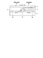
- FIG. 1 is a schematic configuration diagram of a projection display device using a reflective liquid crystal display element as an example of a liquid crystal display device.
- a projection display device 10 includes a reflective liquid crystal display element 11, a polarization beam splitter (hereinafter referred to as PBS) 16, and a projection lens 17.
- PBS polarization beam splitter
- the emitted light L2 emitted from the projection lens 17 is a screen. 18 is projected.
- the reflective liquid crystal display element 11 includes a plurality of pixel electrodes 12 having conductivity and light reflectivity, a liquid crystal layer 13, and a common electrode (transparent electrode) having conductivity and light transmittance common to the plurality of pixel electrodes 12. ) 14 and the pixel circuit 15.
- the plurality of pixel electrodes 12 are arranged in a two-dimensional matrix on the surface of a first substrate (not shown).
- FIG. 1 shows only one arbitrary pixel electrode among the plurality of pixel electrodes 12.
- the common electrode 14 is formed on the surface of a second substrate (not shown).
- the liquid crystal layer 13 is sealed in a space between substrates formed by separating the first substrate and the second substrate so that the pixel electrode 12 and the common electrode 14 face each other.
- Each surface of the pixel electrode 12 and the common electrode 14 is covered with an alignment film (not shown).
- incident light L1 from a backlight or the like emitted from an illumination optical system enters the PBS 16.
- the incident light L1 includes an S-polarized component and a P-polarized component whose planes of polarization are orthogonal to each other.
- the P-polarized light component is schematically shown by a line segment, and the S-polarized light component is shown by a circle.
- the PBS 16 has an optical characteristic of reflecting the S-polarized component of incident light and transmitting the P-polarized component. Accordingly, the PBS 16 reflects the S-polarized component of the incident light L 1 and makes it incident on the common electrode 14.
- the reflective liquid crystal display element 11 causes the S-polarized component incident on the common electrode 14 to be incident on the pixel electrode 12 and reflected through the liquid crystal layer 13, and the reflected light from the pixel electrode 12 passes through the liquid crystal layer 13 and the common electrode 14. Eject through.
- the S-polarized light component incident on the common electrode 14 is modulated according to the potential difference between the drive voltage corresponding to the voltage and the common voltage applied to the common electrode 14. As a result, part of the S-polarized component is converted to the P-polarized component, and light composed of the S-polarized component and the P-polarized component is emitted.
- the PBS 16 transmits the P-polarized component of the light emitted from the reflective liquid crystal display element 11 and enters the projection lens 17, and the S-polarized component reflects and enters the illumination optical system.
- the projection lens 17 projects the P-polarized component from the PBS 16 onto the screen 18 as the emitted light L2, and displays an image.
- the “output light intensity” described later refers to the illuminance of the emitted light L2 measured on the screen 18.
- FIG. 2 is a configuration diagram of one pixel of an embodiment of the liquid crystal display device according to the present invention.
- one pixel 20 of one embodiment of the liquid crystal display device according to the present invention includes a pixel circuit 15 and a liquid crystal element LC, and one column data line D and one row selection line W. It is arranged at the intersection.
- the liquid crystal element LC may have a known configuration. That is, the first substrate and the second substrate so that the pixel electrode 12 having light reflection characteristics formed on the first substrate and the common electrode 14 having light transmission characteristics formed on the second substrate face each other.
- the liquid crystal layer 13 is sealed in the space between the substrates formed by being spaced apart from each other. Note that one pixel 20 in FIG. 2 corresponds to one pixel of the reflective liquid crystal display element 11 shown in FIG.
- the pixel circuit 15 includes a first switching unit 21, a first sample hold unit 22, a second switching unit 23, and a second sample hold unit 24, as shown in FIG.
- the first switching unit 21 has an N-channel MOS field effect in which the drain is connected to the column data line D, the gate is connected to the row selection line W, and the source is connected to the input terminal of the first sample hold unit 22. It is comprised from the transistor (henceforth an NMOS transistor).
- the configuration comprising the first switching unit 21 and the first sample hold unit 22 is the first holding unit
- the second switching unit 23 is the transfer unit
- the second sample hold unit 24 is the second sample hold unit 24. 2 holding means.
- the first sample-and-hold unit 22 includes a flip-flop having an SRAM (Static Random Access Memory) structure, and is connected to the row selection line W and to the column data line D through the first switching unit 21. Yes.
- the first sample-and-hold unit 22 is connected to the sub data line D on the column data line D that is input through the first switching unit 21 when the pixel 20 is selected by a row selection signal applied through the row selection line W.
- Sample and hold frame data (pixel data voltage).
- the second switching unit 23 has a drain connected to the output terminal of the first sample hold unit 22, a gate connected to the common signal line T, and a source connected to the input terminal of the second sample hold unit 24. It consists of NMOS transistors. The second switching unit 23 is activated when an H-level transfer signal is applied via the common signal line T, and the subframe data (pixel data voltage) held in the first sample hold unit 22 is activated. ) Is transferred to the second sample hold unit 24.
- the second sample and hold unit 24 includes a flip-flop having an SRAM structure, samples and holds the subframe data (pixel data voltage) input through the second switching unit 23, and applies it to the pixel electrode 12 of the liquid crystal element LC. To do.
- the voltage applied to the pixel electrode 12 by the second sample hold unit 24 is Vss which is the ground voltage of the MOS transistor when the data to be held is “0”, and the MOS transistor when the data is “1”.
- the power supply voltage Vdd is Vdd.
- the value of the voltage of the common electrode 14 of the liquid crystal element LC is called a common voltage Vcom.
- FIG. 3 is an explanatory diagram showing an example of a method for setting Vdd and Vcom of the reflective liquid crystal display element 11.
- FIG. 3A is an example showing the relationship between the input voltage and the intensity (luminance) of the output light.
- the horizontal axis represents the input voltage, and shows the potential difference between the pixel electrode 12 and the common electrode 14, that is, the driving voltage of the liquid crystal layer 13.
- the vertical axis in FIG. 3A indicates the intensity of the output light emitted from the liquid crystal layer 13.
- the voltage when the intensity of the output light emitted from the liquid crystal layer 13 is the darkest is Vb (black voltage), and the voltage at which the intensity of the output light is saturated is Vw (white voltage).
- FIG. 3B is a diagram for explaining the operation at the time of polarity reversal during white / black driving.
- the power supply voltage Vdd of the pixel circuit is set to (Vw ⁇ Vb), and Vss is set to GND.
- ⁇ Vb is set to the low level VcomL of the common voltage Vcom
- Vw is set to the high level VcomH.
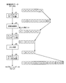
- FIG. 4 shows a block diagram of an embodiment of the liquid crystal display device according to the first embodiment of the present invention.
- the liquid crystal display device 30 of the present embodiment includes a lookup table unit 31, a dithering processing unit 35 including an error diffusion unit 32, a frame rate control unit 33, and a limiter unit 34, and a driving floor.
- a sub-frame data generation unit 36 including an adjustment table 37, a memory control unit 38, frame buffers 39A and 39B having a double buffer configuration, a drive control unit 40, a data transfer unit (not shown), a data inversion unit 42, And a common voltage selector 43.
- the liquid crystal display device 30 includes the reflective liquid crystal display element 11 shown in FIG.
- the reflective liquid crystal display element 11 includes a source driver 44, a gate driver 45, and an image display unit 46.
- the pixel 20 of the reflective liquid crystal display element 11 has a configuration in which the liquid crystal element LC is connected to the pixel circuit 15 as shown in FIG. 2, but FIG. 4 shows only the common electrode 14 and each pixel circuit.
- the pixel electrode 12 and the liquid crystal layer 13 connected every 15 are not shown.
- a configuration in which the source driver 44 and the gate driver 45 are added to the drive control unit 40 is an image display drive unit.
- the image display unit 46 is connected to each intersection where n + 1 column data lines D0 to Dn extending in the vertical direction of the screen intersect with m + 1 row selection lines W0 to Wm extending in the horizontal direction of the screen.
- Pixel circuit 15 formed. A total of (n + 1) ⁇ (m + 1) pixel circuits 15 are arranged in a matrix on the image display unit 46, and each has the configuration shown in FIG. Further, all the pixel circuits 15 constituting the image display unit 46 are connected to the liquid crystal element LC to constitute the pixel 20, and the common voltage Vcom is applied to the common electrode 14 of the liquid crystal element LC from the common voltage selection unit 43.
- the common signal line T is commonly connected.
- the source driver 44 repeats the development of the input sub-frame data for one row of pixels and outputs it to the column data lines D0 to Dn for one row of pixels in units of one horizontal scanning period (1H). .
- the gate driver 45 for example, from the row selection line at the highest position on the screen toward the row selection line at the lowest position on the screen.
- the row selection signal is switched and supplied one by one for every 1H, and the row selection signal is supplied to all the row selection lines W in one frame period.
- the row selection signal is synchronized with the switching period of the subframe data output from the source driver 44 to the column data lines D0 to Dn.
- a lookup table unit 31 receives N-bit video signal data as an input signal and converts it into (M + F + D) -bit data larger than N.
- M is the number of bits when the number of subframes in one frame period is expressed in binary
- F is the number of bits interpolated by the frame rate control unit 33
- D is the number of bits interpolated by the error diffusion unit 32. Show. M, F, and D are natural numbers.
- FIG. 5 shows an example in which the bit number N of the input video signal data is “8”.
- the bit number D to be interpolated by the error diffusion unit 32 is “4”, and the bit to be interpolated by the frame rate control unit 33.
- the number F is “2”. Further, when the number of subframes is expressed in binary, the number of bits M is “4”, and the drive gradation is 15 (not including black).
- the look-up table unit 31 has a function of realizing the liquid crystal display device 30 having an output characteristic of gamma 2.2 by converting input / output characteristics of the reflective liquid crystal display element 11.
- an arbitrary output characteristic for example, gamma 2.2
- the lookup table unit 31 has a lookup table of 256 ⁇ 10 bits (that is, “2 to the 8th power” gradation x (4 + 2 + 4) bits).
- the look-up table unit 31 converts the input 8-bit image data into 10-bit data and outputs it.
- the error diffusion unit 32 diffuses the information of the lower D bits of the video signal data converted into (M + F + D) bits by the lookup table unit 31 to peripheral pixels according to the error diffusion method, thereby obtaining (M + F) bit data. Convert to In the example of FIG. 5, the error diffusion unit 32 diffuses the information of the lower 4 bits of the 10-bit data converted by the lookup table unit 31 to the peripheral pixels, quantizes it into the upper 6-bit data, and outputs it. .
- the output data of the error diffusion unit 32 includes 1-bit carry bit in 6-bit data.
- the error diffusion method is a method of compensating for the lack of gradation by diffusing an error (display error) between a video signal to be displayed and an actual display value to surrounding pixels.
- the error diffusion unit 32 regards the value of the lower 4 bits of the target pixel of the video signal to be displayed as a display error, and displays the display error in the pixel on the right side of the target pixel as shown in FIG. 7/16 times the value, 3/16 times the display error in the lower left pixel, 5/16 times the display error in the lower pixel, and 1/16 times the display error in the lower right pixel Error diffusion is performed by adding the values of.
- the error diffusion unit 32 diffuses the display error of the pixel at a certain coordinate in the 10-bit video signal data to the peripheral pixels as described with reference to FIG. 7 and adds to the error diffused from the peripheral pixels. . That is, in FIG. 8, the input 10-bit video signal data is first added by the adder 322 with the error diffused from the peripheral pixels read from the error buffer 321.
- the addition unit 322 generates 11-bit data in which a carry bit of 1 bit is added to the 10-bit data after addition at the most significant position in consideration of carry when adding. Subsequently, the added video signal data output from the adder 322 is divided into upper 7 bits and lower 4 bits, the upper 7 bits are supplied to the adder 324, and the lower 4 bits are the threshold comparator 323. To be supplied.
- the divided lower 4 bits are shown below.
- the value on the right is a display error.
- the threshold comparison unit 323 supplies the display error corresponding to the divided lower 4 bits to the error buffer 321, diffuses the error to the surrounding pixels according to FIG. 7, and adds the display error to the previous display error and holds it. Let Further, the threshold comparison unit 323 performs threshold comparison on the divided lower 4 bits.
- the comparison unit 323 outputs “1” to the addition unit 324 and adds “1” to the divided upper 7-bit value.
- the adder 324 generates 7-bit data and outputs the data after error diffusion by the error diffusion unit 32.
- the frame rate control unit 33 includes a frame rate control table, and the video signal data after error diffusion converted to (M + F) +1 bits supplied from the error diffusion unit 32 is converted into M + 1 bit data according to the frame control method.
- the frame rate control method refers to j (j: j ⁇ 2, natural number) frame as one period for display of one pixel of the display element, and k (j: k> 0, j> k) of the period.
- ON display is performed and OFF display is performed in the remaining (j ⁇ k) frames to display pseudo gradations in the time direction, and at the same time, j is applied to a plurality of pixels of the display element.
- the frame rate control unit 33 specifies the position in the frame rate control table from the value of the lower F bits of the input video signal data after error diffusion, the pixel position information, and the frame count information, In addition to the upper (M + 1) bits of the error-diffused video signal data, the value (“1” or “0”, hereinafter referred to as “0/1”) is added to the value (M + 1) bits of data. Convert to
- the frame rate control unit 33 includes information on lower 2 bits of the 7-bit error diffused video signal data output from the error diffusion unit 32, position information of the target pixel in the display area, and the frame Based on the counter information, a value of 0/1 is derived from the frame rate control table and added to the upper 5-bit value separated from the input 7-bit error-diffused video signal data.
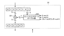
- the frame rate control unit 33 first divides the inputted 7-bit error diffused video signal data into upper 5 bits and lower 2 bits, and supplies the upper 5 bits of data to the adder 331.
- the lower 2 bits of data are supplied to the frame rate control table unit 332.
- the frame rate control table unit 332 determines which pixel is the target pixel when the lower 2 bits of the input video signal data after error diffusion of 7 bits and the display area are divided into 4 parts in the vertical direction and 4 parts in the horizontal direction.
- the position information (that is, the lower 2 bits of the X coordinate that is the coordinate data and the lower 2 bits of the Y coordinate) that is included in the divided range and the lower 2 bits of the frame counter, and a total of 8 bits, A value of “0” or “1” shown in the frame rate control table of FIG. 10 is specified.
- the lower 2 bits are (00, 11)
- the lower 2 bits “0” of the X coordinate and the Y coordinate in FIG. Is the value of the position of the lower 2 bits of “3”.
- the “lower 2 bits” in the vertical direction indicate the lower 2 bits of the input 7-bit data
- the “lower 2 bits” in the horizontal direction indicate the lower 2 bits of the frame counter.
- the adding unit 331 adds the value of “0” or “1” specified by the frame rate control table unit 332 to the upper 5 bits of the input video signal data after error diffusion of 7 bits, The 5-bit data after the addition is output as output data of the frame rate control unit 33.
- the limiter unit 34 shown in FIGS. 4 and 5 limits the value of the 5-bit data output from the frame rate control unit 33 to, for example, “15”, which is the maximum value of the drive gradation, and the 4 bits after the limitation.
- the data is output to the subframe data generation unit 36.
- the error diffusion unit 32, the frame rate control unit 33, and the limiter unit 34 constitute a dithering processing unit 35 as shown in FIG. 4, and are supplied from the lookup table unit 31 by the above operation.
- a so-called dithering process is performed on the 10-bit video signal data after the gradation interpolation to perform a visual psychological calculation in the time direction or the spatial direction to generate 4-bit data in which the gradation is interpolated. Thereby, improvement in image quality can be realized.
- the subframe data generation unit 36 shown in FIG. 4 uses a drive gradation table 37 described later, and converts the 4-bit data output from the limiter unit 34 to, for example, the maximum gradation “15” as shown in FIG. It is converted into 15-bit data as shown.
- This 15-bit data is 1 indicating whether or not the target pixel is displayed in a subframe assigned corresponding to the bit position among 15 subframes each having a display period obtained by dividing one frame period into 15 parts. This is data consisting of 15 bit subframe data.
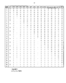
- FIG. 6 shows a specific example of the drive gradation table 37 used in the subframe data generation unit 36.
- the horizontal axis indicates the data value (the driving period when 1 and the blanking period when 0) in each of the subframes SF1 to SF15
- the vertical axis indicates the gradation.
- the gradation on the vertical axis indicates a gradation generated by the frame rate control unit 33 and limited by the limiter unit 34 to “15” which is the maximum value of the drive gradation.
- the drive gradation table 37 shown in FIG. 6 divides one frame of a video signal into 15 sub-frames SF1 to SF15 each having a display period shorter than one frame period, so that gradations 0 to 15 are divided.
- a driving gradation table 37 in the case of performing 16 gradation display is shown.
- SF1 to SF15 indicate the order of subframes in one frame.
- the drive gradation table 37 is set so that the number of subframes to be driven increases sequentially from SF1 as the gradation to be displayed increases. For example, when the gradation is “6”, driving is performed in 6 subframes from subframes SF1 to SF6, and is not driven in 8 subframes of subframes SF7 to SF14. When the gradation is “7”, driving is performed in 7 subframes from subframes SF1 to SF7, and is not driven in 7 subframes of subframes SF8 to SF14. Similarly, the number of subframes in the drive state increases as the number of gradations increases, and all subframes SF1 to SF15 are driven at the maximum gradation of “15”. In other words, as the number of gray levels increases, the number of subframes that are in the driving state increases backward in time.
- the subframe data generation unit 36 drives the 1-bit subframe data in each of the subframes SF1 to SF15 corresponding to the gradation indicated by the 4-bit data supplied from the dithering processing unit 35 as shown in FIG.
- the data is acquired using the gradation table 37 and a total of 15-bit data is output to the memory control unit 38.
- the subframe data generation unit 36 converts the 4-bit input data into a decimal number, and the gradation “ 6 ”is converted to 15-bit data [111111,000,000,000] in total indicating whether or not to drive each of SF1 to SF15 with reference to the drive gradation table 37 of FIG. “1” from the first bit of the 15-bit data to the sixth bit means driving by SF1 to SF6, and “0” from the seventh bit to the 15th bit is not driven by SF7 to SF15 Means that.
- the memory control unit 38 supplies, for example, 15 subframe data supplied from the subframe data generation unit 36 to the two frame buffers 39A and 39B.
- the frame buffers 39A and 39B have a double buffer structure.
- the subframe data stored in the other frame buffer is transferred via the data inversion unit 42. Is done.
- the subframe data of one frame buffer stored during the previous frame period is transferred via the data inversion unit 42, and the other frame buffer is transferred from the subframe data generation unit 36. Of subframe data is stored.
- the drive control unit 40 is supplied with the vertical synchronization signal VSYNC and the horizontal synchronization signal HSYNC of the video signal data supplied to the lookup table unit 31, and controls the processing timing and the like for each subframe in synchronization with these synchronization signals.
- the transfer instruction to the data inverting unit 42 and the control of the gate driver 45 are performed.
- the memory control unit 38 is instructed to receive the designated subframe data out of the subframe data read from the frame buffer 39A or 39B by the memory control unit 38. .
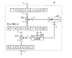
- the data inversion unit 42 follows the data inversion signal from the drive control unit 40, and when the data inversion signal is at a low level, the input subframe data is inverted in polarity (in the case of “0”, “1”, “1” "Is reversed to” 0 ") and transferred to the source driver 44.
- the source driver 44 Each time the source driver 44 receives 1-bit subframe data of pixels for one line in the same subframe from the data inversion unit 42, the source driver 44 supplies the column data lines D0 to Dn to the pixel circuit 15 of the corresponding pixel of the image display unit 46. Use to transfer at the same time.
- the gate driver 45 activates the row selection line Wy of the row y designated by the vertical start signal (VST) / vertical shift clock signal (VCK) from the drive control unit 40, and all the designated rows y are activated. (N + 1) pixels in the column are selected.
- the first switching unit 21 is activated and (n + 1) for one line inputted in parallel from the source driver 44 via the column data lines D0 to Dn. ) Out of the subframe data, the subframe data supplied via the connected column data line is sampled and held in the first sample hold unit 22 for each pixel.
- the common voltage selection unit 43 selects the low level VcomL during the period in which the polarity of the voltage applied to the liquid crystal element LC of the pixel 20 is + as described above, and the polarity is ⁇ . During the period, the common voltage Vcom of the high level VcomH is selected and output to the common electrode 14 of all the pixels 20.
- the above operation is repeated in units of one line, and driving is performed each time data transfer and hold of one subframe to the first sample hold unit 22 in the pixel circuits 15 of all the lines of the image display unit 46 are completed.
- the control unit 40 outputs a transfer signal to the common signal line T, and simultaneously activates the second switching units 23 in the pixel circuits 15 of all the lines. Further, the data of one subframe held in the first sample hold unit 22 is collectively transferred to the second sample hold unit 24 to be sampled and held.
- the subframe data held in the second sample hold unit 24 and applied to the pixel electrode 12 has a value of “1” or “0” depending on the gradation to be displayed in the pixel.
- FIG. 11 is an explanatory diagram showing an example of a drive pattern in the embodiment of the liquid crystal display device according to the present invention.
- FIG. 11 shows a drive pattern when the number of subframes in one frame period is fifteen.
- FIG. 11A shows the polarity inversion signal of the even frame
- FIG. 11F shows the polarity inversion signal of the odd frame.
- the polarity inversion signals supplied to the data inversion unit 42 and the common voltage selection unit 43 are inverted every subframe as shown in FIGS. 11A and 11F, and are divided between even frames and odd frames. The order is reversed.
- FIG. 11B shows the state of even-frame data written to the first sample-and-hold unit 22, and FIG. 11G shows the state of odd-frame data written to the first sample-and-hold unit 22.
- “SF1 +” indicates that the data of the first subframe is held in the first sample hold unit 22 without being inverted by the data inversion unit 42 for polarity + drive.
- “SF2-” in FIG. 11B indicates that the data of the second subframe is inverted by the data inverting unit 42 for polarity-driving and held in the first sample hold unit 22.
- FIG. 11B shows the state of even-frame data written to the first sample-and-hold unit 22
- FIG. 11G shows the state of odd-frame data written to the first sample-and-hold unit 22.
- “SF1 +” indicates that the data of the first subframe is held in the first sample hold unit 22 without being inverted by the data inversion unit 42 for polarity + drive.
- SF1- indicates that the data of the first subframe is inverted by the data inversion unit 42 for polarity-drive and held in the first sample hold unit 22.
- SF2 + indicates that the data of the second subframe is held in the first sample hold unit 22 without being inverted by the data inversion unit 42 for polarity + drive. Show. As can be seen from FIGS. 11B and 11G, the data of the first to fifteenth subframes SF1 to SF15 held in the first sample hold unit 22 for each subframe is inverted for each subframe. ing.
- FIG. 11C shows the state of even-numbered frame data written to the second sample-and-hold unit 24, and FIG. 11H shows the state of odd-numbered frame data written to the second sample-and-hold unit 24.
- the data of the first to fifteenth subframes SF1 to SF15 held in the second sample hold unit 24 for each subframe is the first sample hold unit.
- the data of the first to fifteenth subframes SF1 to SF15 held at 22 is held with a delay of one subframe.
- FIG. 11D shows the polarity of the common voltage Vcom when an even frame video signal is input
- FIG. 11I shows the polarity of the common voltage Vcom when an odd frame video signal is input
- “H” indicates that the common voltage Vcom is the high level VcomH
- “L” indicates that the common voltage Vcom is the low level VcomL.
- the polarity of the common voltage is synchronized with the polarity inversion signal. When the polarity inversion signal is low level, VcomH, and when the polarity inversion signal is high level, VcomL. In addition, the order of the even frame and the odd frame is reversed.
- VcomH is applied to the common electrode without inverting the data.
- VcomH is applied to the common electrode without inverting the data.
- the polarity inversion signal is at a high level
- VcomH is applied to the common electrode without inverting the data.
- the polarity inversion signal is at a low level
- the data is inverted and applied to the common electrode.
- a drive pattern for applying VcomL may be used.
- FIG. 11E shows a driving state of the liquid crystal element LC when an even frame image signal is displayed
- FIG. 11J shows a driving state of the liquid crystal element LC when an odd frame image signal is displayed
- “DC +” indicates a driving period in which the polarity of the liquid crystal applied voltage is driven as +
- “DC ⁇ ” indicates a driving period in which the polarity of the liquid crystal applied voltage is driven as ⁇ .
- the drive polarity is + when the common voltage is VcomL, and ⁇ when the common voltage is VcomH, and the order is reversed between the even frame and the odd frame. ing.
- the drive polarity is inverted for each subframe so that the liquid crystal element LC is AC driven. Furthermore, since the drive polarity is inverted for each frame, it is possible to further effectively prevent burn-in.
- the drive control unit 40 controls the memory control unit 38 via a data transfer unit (not shown) to perform subframes.
- the subframe data of the subframe SF1 is sequentially output from the buffer 39A or 39B in units of pixels, and a polarity inversion signal is generated and output to the data inversion unit 42 and the common voltage selection unit 43, respectively.
- the drive control unit 40 starts from the time T0 as shown in FIG. 12B as described with reference to FIG.
- a low-level polarity inversion signal is output.
- the memory control unit 38 receives the subframe data of the designated subframe SF1 from the frame buffer 39A or 39B, and transfers it to the data inversion unit 42. Since the polarity inversion signal supplied at this time is at a low level, the data inversion unit 42 outputs the subframe data of the subframe SF1 to the source driver 44 without data inversion.
- FIG. 12C shows 1-bit subframe data before inversion processing in a pixel at a certain coordinate (x, y) position output from a data transfer unit (not shown), and FIG. The sub-frame data of a pixel at a certain coordinate (x, y) position that is inverted by the data inversion processing unit 42 and supplied to the source driver 44 is shown.
- the subframe data SF1 to SF15 of the pixel at a certain coordinate (x, y) position output from the data transfer unit (not shown) is as shown in FIG. 12C within one frame period. Assuming that it changes as [111100000000000000], the polarity inversion signal is inverted every subframe as shown in FIG. 11B and is [01010101010].
- the pixel data transferred to the driver 44 is [1010010101010] as shown in FIG.
- the source driver 44 Each time the source driver 44 stores SF1 subframe data for one line, the source driver 44 simultaneously transfers to the pixel circuit 15 of the corresponding pixel of the image display unit 46 using the column data lines D0 to Dn. At this time, the gate driver 45 supplies a row selection signal to the row selection line Wy of the row y designated by the vertical start signal (VST) / vertical shift clock signal (VCK) from the drive control unit 40 to activate it, Select (n + 1) pixels in all columns of the specified row y.
- VST vertical start signal
- VK vertical shift clock signal
- the first switching unit 21 is activated and (n + 1) for one line inputted in parallel from the source driver 44 via the column data lines D0 to Dn.
- the sub-frame data supplied through the connected column data line is sampled among the sub-frame data of SF1 and held in the first sample hold unit 22 for each pixel.
- FIG. 12E shows a row selection signal supplied to a row selection line Wy of a certain designated row y at time T1
- FIG. 12G shows the pixel at a certain coordinate (x, y) position. Data held by the first sample hold unit 22 in the pixel circuit 15 is shown.
- FIG. 12I shows the data held in the second sample hold unit 24 in the pixel circuit 15 of the pixel at a certain coordinate (x, y) position.
- the subframe data of the subframe SF1 held in the second sample hold unit 24 is applied as a pixel voltage to the corresponding pixel electrode 12 connected to the pixel circuit 15 to drive the liquid crystal element LC.
- Vcom of high level VcomH Vw
- the second sample hold units 24 in all the pixel circuits 15 of the image display unit 46 store the last subframe of the previous frame.
- the data of SF15 is stored (here, explicitly set to “1”).
- the pixel electrode 12 in the pixel circuit 15 of a certain pixel corresponds to data having a value of “1” as shown in FIG.
- the drive control unit 40 controls the memory control unit 38 via a data transfer unit (not shown) in one subframe period from time T2 to time T3, and then transfers the next subframe from the frame buffer 39A or 39B.
- the sub-frame data of SF2 is sequentially output for each pixel, and a high-level polarity inversion signal is generated and output to the data inversion unit 42 and the common voltage selection unit 43 as shown in FIG.
- Data is written in units of one line to all the pixel circuits 15 of the image display unit 46.
- the drive control unit 40 outputs a high-level common transfer signal to the common signal line T as shown in FIG. 12 (H) at time T3, and all the pixel circuits 15 of the image display unit 46.
- the second switching units 23 in all the pixel circuits 15 of the image display unit 46 are simultaneously activated and are held by the first sample hold units 22 in all the pixel circuits 15 of the image display unit 46.
- the subframe data of the subframe SF2 is simultaneously transferred to the second sample hold unit 24 to be updated and held.
- the second sample hold unit 24 holds the subframe data of the subframe SF1 and the corresponding pixel electrode connected to the pixel circuit 15. 12 is applied as a pixel voltage.
- the drive control unit 40 controls the memory control unit 38 with the control signal CTL to transmit the subframe data of the next subframe SF3 from the frame buffer 39A or 39B.
- a low-level polarity inversion signal is generated and output to the data inversion unit 42 and the common voltage selection unit 43 as shown in FIG.
- the polarity-DC balance drive of subframe SF2 is performed. That is, in each pixel, the polarity of the voltage applied to the liquid crystal layer 13 is reversed between SF1 and SF2, but the same white display or black display is performed.
- the polarity negative DC balance driving and the polarity positive DC balance driving are alternately performed for each subframe.
- the liquid crystal layer 13 of the liquid crystal element LC in each pixel circuit 15 is AC driven by applying a voltage whose polarity is alternately inverted in subframe units, thereby preventing burn-in. Can do.
- the polarity-balanced DC balance driving period when the subframe data applied to the pixel electrode 12 is “0”, the white display period is set, and when the subframe data is “1”, the black display period is set. It becomes a period.
- the DC balance driving period of polarity + when the sub-frame data applied to the pixel electrode 12 is “0”, it is a black display period, and when it is “1”, it is a white display period.
- the period (from time T0 to time T2) is the data transfer period, and the drive period is the period from time T2 to time T3 with a delay of one subframe period. Therefore, the subframe data transfer period of all subframes from SF1 to SF15 is a period from time T0 to time T5, and the driving period is a period from time T2 to time T6.
- Time T6 is a time one subframe period after time T5. Looking at the voltage applied to the pixel liquid crystal in the period shown in FIG. 12L (from time T2 to time T6), subframes SF1 to SF4 are white display periods, and subframes SF5 to SF15 are black display periods. This matches the data before inversion processing shown in FIG.
- FIG. 13 is an explanatory diagram of a mechanism for generating a lateral electric field in the reflective liquid crystal element LC.
- the pixel electrode 12a of the reflective liquid crystal element LC of the pixel PA and the pixel electrode 12b of the reflective liquid crystal element LC of the pixel PB are formed on the silicon substrate 51.
- the PA and PB common electrodes 14 are spaced apart from each other.
- a liquid crystal layer 13 is sealed between the pixel electrodes 12 a and 12 b and the common electrode 14.
- the drive state (drive / blanking) often changes between adjacent pixels.
- the driving states of adjacent pixels PA and PB shown in FIG. 13 are different, the pixel PA is in a blanking state, and the pixel PB is in a driving state.
- the pixel voltage Vss is applied to the pixel electrode 12a of the pixel PA in the blanking state, and the pixel voltage Vdd is applied to the pixel electrode 12b of the pixel PB in the driving state.
- a potential difference is generated between the pixel electrode 12b of the pixel PB in the driving state and the common electrode 14, and an electric field 52 is generated in the liquid crystal layer 13, whereby the liquid crystal is rotated by a predetermined amount.
- a potential difference is also generated between the pixel electrode 12 a of the pixel PA in the blanking state and the pixel electrode 12 b of the pixel PB, and an electric field 53 is generated in the lateral direction with respect to the electric field 52.
- This phenomenon occurs similarly in the case of polarity-balanced DC balance driving.
- Such a lateral electric field 53 causes unintended confusion in the movement of the liquid crystal between pixels. The above phenomenon contributes to image quality degradation.
- the frame rate control by the frame rate control unit 33 can uniformly distribute the horizontal electric field as described with reference to FIG. Can be resolved.
- FIG. 14 illustrates the case where the value of the lower F bits of the input data ((M + F) bits) to the frame rate control unit 33 is “01”.
- the frame rate control unit 33 switches between four frame rate control tables (frames 0 to 3) for each frame.
- the driving state driving or blanking
- the driving state is changed to “0” from the pixel whose driving state is “1” (driving state) as described in FIG. ”(Blanking state)
- a horizontal electric field is generated in the direction of the pixel.
- the arrows in FIG. 14A are shown in FIG. 14A for frame 0, FIG. 14B for frame 1, FIG. 10C for frame 2, and FIG.
- a lateral electric field is generated in the direction shown.
- the frame rate control unit 33 determines the position in the frame rate control table from the lower F bit value of the (M + F) bit video signal data input as described above, the pixel position information, and the frame count information. Then, the value is added to the upper M bits of the input video signal data and converted to M bit data.
- the value obtained by specifying the position in the frame rate control table is an average of a total of four frames from frame 0 to frame 3, and the state of the transverse electric field in these four frames is superimposed. This is the value shown in FIG. As shown in FIG. 14E, in the average of four frames, the horizontal electric field between all the pixels is dispersed and cancels out. As described above, by using the frame rate control, it is possible to disperse and cancel the lateral electric field that is a cause of image quality degradation.
- the latch circuit can be configured as follows.
- the voltage selection unit necessary for the pixel of the liquid crystal display device can be eliminated, the number of transistors in the pixel circuit can be reduced as compared with the conventional liquid crystal display device, so that the pixel can be downsized and the cost can be reduced. can do.
- the subframe data can be transferred without a pause period of the subframe data, and a subframe of a certain subframe can be transferred.
- the frame data transfer period display based on the subframe data of the immediately preceding subframe is performed. Therefore, data can be transferred more efficiently than the conventional liquid crystal display device, and since there is no driving suspension period, it is possible to prevent the phenomenon that the display becomes dark due to the driving suspension period. Further, according to the liquid crystal display device 30 of the present embodiment, it is possible to improve image quality degradation due to a horizontal electric field by frame rate control.
- the polarity + DC balance drive and the polarity ⁇ DC balance drive are alternately performed for each subframe. At the same time, since the order is reversed every frame, burn-in can be sufficiently prevented.
- liquid crystal display device 30 of the present embodiment having the above features, it is possible to realize a stereoscopic image display device with high resolution and high brightness at low cost.
- FIG. 16 is an explanatory diagram of an example of a method for setting Vdd and Vcom of the reflective liquid crystal display element 11 in the second embodiment.
- FIG. 16A is an example showing the relationship between the input voltage and the intensity (luminance) of the output light.
- the horizontal axis represents the input voltage, and shows the potential difference between the pixel electrode 12 and the common electrode 14, that is, the driving voltage of the liquid crystal layer 13.
- the vertical axis in FIG. 16A indicates the intensity of output light emitted from the liquid crystal layer 13.
- the voltage when the intensity of the output light emitted from the liquid crystal layer 13 is the darkest is Vb (black voltage), and the voltage at which the intensity of the output light is saturated is Vw (white voltage).
- Vm intermediate voltage
- Vthreshold voltage for rewriting data to be sampled and held in the middle of Vw (white voltage) and Vb (black voltage).
- FIG. 16B is a diagram for explaining the operation at the time of polarity reversal during white / black driving.
- polarity inversion driving DC balance driving
- the second voltage VcomH (H) Vw is applied to the common voltage Vcom as the high level VcomH.
- FIG. 17C is a diagram for explaining the operation at the time of polarity reversal during intermediate / black driving.
- polarity inversion driving DC balance driving
- the configuration of the liquid crystal display device according to the second embodiment will be described. 17 the difference from the configuration of the liquid crystal display device according to the first embodiment shown in FIG. 4 is that the VcomH voltage selection unit 43a (high level common voltage selection) is added to the common voltage selection unit 43 that applies the common voltage Vcom. Part).
- a Vdd voltage selection unit 48 for applying the pixel voltage Vdd is provided.
- a drive table 41 for operating the drive control unit 40 is provided.
- a lookup table unit 31 receives N-bit video signal data as an input signal and converts it into (M + F + D) bit data larger than N.
- M is the number of bits when the drive gradation number is expressed in binary
- F is the number of bits to be interpolated by the frame rate control unit 33
- D is the number of bits to be interpolated by the error diffusion unit 32.
- M, F, and D are natural numbers.
- FIG. 18 shows an example in which the number of bits N of the input video signal data is “8” and the number of drive gradations is “31”.
- the number of bits D to be interpolated by the error diffusion unit 32 is “4” and the frame rate.
- the number of bits F to be interpolated by the control unit 33 is “2”.
- the bit number M when the drive gradation number is expressed in binary is “5”.
- the look-up table unit 31 is adjusted in advance so that the 11-bit output has an arbitrary output characteristic (for example, gamma 2.2).
- images of 29 drive gradations (not including black) in the drive gradation table 37 of FIG. 19 are projected onto the screen 18 in the projection display device 10 shown in FIG.
- the illuminance on the screen 18 is measured with an illuminometer or the like.
- the lookup table unit 31 has a lookup table of 256 ⁇ 11 bits (that is, “2 to the 8th power” gradation x (5 + 2 + 4) bits).
- the lookup table unit 31 converts the input 8-bit image data into 11-bit data and outputs it.
- the error diffusion unit 32 diffuses the information of the lower D bits of the video signal data converted into (M + F + D) bits by the lookup table unit 31 to peripheral pixels according to the error diffusion method, thereby obtaining (M + F) bit data. Convert to In the example of FIG. 18, the error diffusion unit 32 diffuses the lower 4 bits of the 11-bit data converted by the lookup table unit 31 to surrounding pixels, quantizes them into upper 7-bit data, and outputs the data. .
- the output data of the error diffusion unit 32 includes 1-bit carry bit in 7-bit data.
- the error diffusion unit 32 diffuses the display error of the pixel at a certain coordinate in the 11-bit video signal data to the peripheral pixels as described with reference to FIG. 7 and adds to the error diffused from the peripheral pixels. . That is, in FIG. 20, the input 11-bit video signal data is first added by the adder 322 with the error diffused from the peripheral pixels read from the error buffer 321.
- the addition unit 322 generates 12-bit data in which a carry bit of 1 bit is added to the 11-bit data after addition at the most significant position in consideration of carry when adding. In FIG. 20, the carry bit 0 is added to the 11-bit data after the adder 322 #. Subsequently, the added video signal data output from the adder 322 is divided into upper 8 bits and lower 4 bits, The upper 8 bits are supplied to the adder 324, and the lower 4 bits are supplied to the threshold comparator 323.
- the divided lower 4 bits are shown below.
- the value on the right is a display error.
- the threshold comparison unit 323 supplies the display error corresponding to the divided lower 4 bits to the error buffer 321, diffuses the error to surrounding pixels according to FIG. 7, and adds the display error to the previous display error and holds it. .
- the threshold comparison unit 323 performs a threshold comparison on the divided lower 4 bits value, and the divided lower 4 bits value is larger than “1000” (the 4-bit value in the above table is “ “1” is output to the adder 324, and “1” is added to the divided upper 8 bits.
- the adder 324 generates 8-bit data and outputs the data after error diffusion by the error diffusion unit 32.
- the frame rate control unit 33 includes information on lower 2 bits of the 8-bit error diffused video signal data output from the error diffusion unit 32, position information on the target pixel in the display area, and the frame. Based on the counter information, a value of 0/1 is derived from the frame rate control table and added to the upper 6-bit value separated from the input 8-bit error-diffused video signal data.
- the frame rate control unit 33 first divides the input 8-bit error-diffused video signal data into upper 6 bits and lower 2 bits, and supplies the upper 6 bits of data to the adder 331.
- the lower 2 bits of data are supplied to the frame rate control table unit 332.
- the adding unit 331 adds the value of “0” or “1” specified by the frame rate control table unit 332 to the upper 6 bits of the input video signal data after error diffusion of 8 bits, The 6-bit data after the addition is output as output data of the frame rate control unit 33.
- the limiter unit 34 shown in FIGS. 17 and 18 limits the value of the 6-bit data output from the frame rate control unit 33 to, for example, “31”, which is the maximum value of the drive gradation, and 5 bits after the limitation.
- the data is output to the subframe data generation unit 36.
- the error diffusion unit 32, the frame rate control unit 33, and the limiter unit 34 constitute a dithering processing unit 35 as shown in FIG. 17, and are supplied from the lookup table unit 31 by the above operation.
- a so-called dithering process is performed on the 11-bit video signal data after the gradation interpolation to perform a visual psychological calculation in the time direction or the spatial direction, thereby generating 5-bit data in which the gradation is interpolated. Thereby, improvement in image quality can be realized.
- the subframe data generation unit 36 shown in FIG. 17 uses the drive gradation table 37 to convert the 5-bit data output from the limiter unit 34 into, for example, 16 indicating the maximum gradation “31” as shown in FIG. Convert to bit data.
- This 16-bit data is 1 indicating whether or not the target pixel is displayed in the subframe assigned corresponding to the bit position among the 16 subframes each having a display period obtained by dividing one frame period into 16. This is data consisting of 16 bit subframe data.
- FIG. 19 shows a specific example of the drive gradation table 37 used in the subframe data generation unit 36.
- the horizontal axis indicates the data value (the driving period when 1 and the blanking period when 0) in each of the subframes SF1 to SF16
- the vertical axis indicates the gradation.
- the gradation on the vertical axis indicates a gradation generated by the frame rate control unit 33 and limited by the limiter unit 34 to “31” which is the maximum value of the drive gradation.
- the drive gradation table 37 shown in FIG. 19 divides one frame of a video signal into 16 sub-frames SF1 to SF16 each having a display period shorter than one frame period, so that gradations 0 to 31 are divided.
- a drive gradation table 37 for performing 32 gradation display is shown.
- SF1 to SF16 indicate the order of subframes in one frame.
- the drive gradation table 37 is divided into SF1 having a weight of “1” and SF2 to SF16 having a weight of “2”, and expresses gradation by a combination of subframes having different weights.
- SF2 to SF16 are set such that the number of subframes to be driven increases sequentially from SF2 as the gradation to be displayed increases. For example, when the gradation is “6”, driving is performed in 3 subframes from subframes SF2 to SF4, and is not driven in 13 subframes of subframes SF1 and SF5 to SF16.
- gradation When the gradation is “7”, driving is performed in 4 subframes from subframes SF1 to SF4, and is not driven in 12 subframes of subframes SF5 to SF16. In the maximum gradation “31”, all the subframes SF1 to SF16 are driven. In other words, as the number of gradations increases, SF1 is in a driving state only when the number of gradations is an odd number, and the subframes that are in a driving state after SF2 increase backward in time.
- the subframe data generation unit 36 drives the 1-bit subframe data in each of the subframes SF1 to SF16 corresponding to the gradation indicated by the 5-bit data supplied from the dithering processing unit 35 as shown in FIG. Acquired using the gradation table 37 and outputs a total of 16-bit data to the memory control unit 38.
- the subframe data generation unit 36 refers to the drive gradation table 37 of FIG. Converted to 16-bit data [1111,000,000,000,000] indicating whether or not to drive each of SF16. “1” from the first bit to the fourth bit of 16-bit data means driving by SF1 to SF4, and “0” from the fifth bit to the 16th bit is not driven by SF5 to SF15 Means that.
- the drive control unit 40 is supplied with the vertical synchronization signal VSYNC and the horizontal synchronization signal HSYNC of the video signal data supplied to the lookup table unit 31, and controls the processing timing and the like for each subframe in synchronization with these synchronization signals.
- the control signal CTL is sent to the memory control unit
- the data inversion signal is sent to the data inversion unit 42
- the polarity inversion signal is sent to the common voltage selection unit 43, the VcomH voltage selection unit 43a and the Vdd voltage selection unit 48.
- the white / intermediate voltage selection signal is controlled, and the source driver 44 and the gate driver 45 are controlled.
- the memory control unit 38 supplies, for example, 16 subframe data supplied from the subframe data generation unit 36 to the two frame buffers 39A and 39B.
- the frame buffers 39A and 39B have a double buffer structure.
- the subframe data stored in the other frame buffer is a control signal from the drive control unit 40.
- the data is transferred via the memory control unit 38 in accordance with CTL.
- the subframe data of one frame buffer stored during the previous frame period is transferred via the memory control unit 38 according to the control signal CTL from the drive control unit 40, and the other
- the frame buffer stores subframe data from the subframe data generation unit 36.
- the data inversion unit 42 inverts the subframe data transferred via the memory control unit 38 in accordance with the data inversion signal from the drive control unit 40, and inverts the input subframe data when the data inversion signal is at a high level. ("0" is inverted to "1", and "1" is inverted to "0") and supplied to the source driver 44.
- the source driver 44 Each time the source driver 44 receives 1-bit subframe data of pixels for one line in the same subframe from the data inversion unit 42, the source driver 44 supplies the column data lines D0 to Dn to the pixel circuit 15 of the corresponding pixel of the image display unit 46. Use to transfer at the same time.
- the gate driver 45 activates the row selection line Wy of the row y designated by the vertical start signal (VST) / vertical shift clock signal (VCK) from the drive control unit 40, and all the designated rows y are activated. (N + 1) pixels in the column are selected.
- the first switching unit 21 is activated and (n + 1) for one line inputted in parallel from the source driver 44 via the column data lines D0 to Dn. ) Out of the subframe data, the subframe data supplied via the connected column data line is sampled and held in the first sample hold unit 22 for each pixel.
- the VcomH voltage selection unit 43a and the Vdd voltage selection unit (power supply voltage selection unit) 48 follow the white / intermediate voltage selection signal from the drive control unit 40.
- the VcomH voltage selection unit 43a selects VcomHH.
- the output is VcomH
- the Vdd voltage selector 48 selects VddH (high level) and outputs it as Vdd.
- the VcomH voltage selection unit 43a selects VcomHL and outputs it as VcomH
- the Vdd voltage selection unit 48 selects VddL (low level) and outputs it as Vdd.
- the common voltage selection unit 43 selects the low level VcomL during the period in which the polarity of the voltage applied to the liquid crystal element LC of the pixel 20 is + as described above, and the polarity is ⁇ . During the period, the common voltage Vcom of the high level VcomH is selected and output to the common electrode 14 of all the pixels 20.
- FIG. 22 shows an example of the drive table 41 held in the drive control unit 40.
- FIG. 22 shows a driving table when the number of subframes in one frame period is 16, SF1 is weighted “1”, SF2 to SF16 are weighted “2”, and the refresh rate is 60 Hz and one frame period is 16.667 [ms].
- Show. 22A to 22F show drive tables for even frames
- FIGS. 22K to 22P show drive tables for odd frames.
- 22A and 22K show the driving subframe order, and the subframes driven in order from the top.
- 22B and 22L show subframe data read from the frame buffer 39A or 39B by the memory control unit 38 of FIG. 17 and transferred to the image display unit 46 via the data inversion unit 42. This is shown in order from SF1 to SF16.
- 22 (C) and 22 (M) show a driving period for each subframe, and 1041 [us] is set by dividing one frame period into 16 equal parts.
- 22D and 22N show data inversion signals output from the drive control unit 40 to the data inversion unit 42. The even frames are alternately set from “0” and the odd frames from “1”. Is done.
- 22E and 22O show the polarity inversion signal output from the drive control unit 40 to the common voltage selection unit 43, and a value delayed by one subframe period of the data inversion signal is set.
- the value of the last data inversion signal of the odd frame is set for the even frame
- the value of the last data inversion signal of the even frame is set for the odd frame.
- (F) and (P) in the figure represent white / intermediate voltage selection signals output from the drive control unit 40 to the VcomH voltage selection unit 43a and the Vdd voltage selection unit 48, and the driving order 2 in which SF1 is driven. Only “1” is set.
- FIGS. 22 (G) to (J) and (Q) to (T) are not information that is directly required for the drive table, but FIGS. 22 (G) and 22 (Q) actually show the liquid crystal.
- the sub-frames to be driven are shown.
- the SF 16 transferred at the end of the previous frame is driven at the top, and then SF1 to SF15 are driven in order.
- 22 (H) and (R) show the output of the common voltage selection unit 43
- FIGS. 22 (I) and (S) show the output of the VcomH voltage selection unit 43a
- FIGS. ) Represents the output of the Vdd voltage selection unit 48.
- the drive polarity is inverted for each subframe so that the liquid crystal element LC is AC driven. Furthermore, since the drive polarity is inverted for each frame, it is possible to further effectively prevent burn-in.
- the drive control unit 40 follows the data transfer unit (not shown) via the data transfer unit according to FIG. 22B. 38, the subframe data of the subframe SF1 is sequentially output in units of pixels from the subframe buffer 39A or 39B, and a data inversion signal is generated and output to the data inversion unit 42 according to FIG. 22E, a polarity inversion signal is generated and output to the common voltage selector 43, and a white / intermediate drive signal is generated according to FIG. 22F to generate a VcomH voltage selector 43a and a Vdd voltage selector 48. Output to.
- One subframe period (transfer period WC) from time T0 to time T2 a low-level data inversion signal, a polarity inversion signal, and a white / intermediate drive signal are output.
- the memory control unit 38 receives the subframe data of the designated subframe SF1 from the frame buffer 39A or 39B, and transfers it to the data inversion unit 42. Since the data inversion signal supplied at this time is at a low level, the data inversion unit 42 outputs the subframe data of the subframe SF1 to the source driver 44 as it is without inverting the data.
- FIG. 23E shows 1-bit subframe data before inversion processing in a pixel at a certain coordinate (x, y) position output from a data transfer unit (not shown), and FIG. The sub-frame data of a pixel at a certain coordinate (x, y) position that is inverted by the data inversion processing unit 42 and supplied to the source driver 44 is shown.
- subframe data SF1 to SF16 of a pixel at a certain coordinate (x, y) position output from a data transfer unit (not shown) is as shown in FIG. 23E within one frame period.
- the data inversion signal is inverted every subframe as shown in FIG. 11B and is [101010101010].
- the pixel data transferred to the driver 44 is [10101010100101] as shown in FIG.
- the source driver 44 Each time the source driver 44 stores SF1 subframe data for one line, the source driver 44 simultaneously transfers to the pixel circuit 15 of the corresponding pixel of the image display unit 46 using the column data lines D0 to Dn. At this time, the gate driver 45 supplies a row selection signal to the row selection line Wy of the row y designated by the vertical start signal (VST) / vertical shift clock signal (VCK) from the drive control unit 40 to activate it, Select (n + 1) pixels in all columns of the specified row y.
- VST vertical start signal
- VK vertical shift clock signal
- the first switching unit 21 is activated and (n + 1) for one line inputted in parallel from the source driver 44 via the column data lines D0 to Dn.
- the sub-frame data supplied through the connected column data line is sampled among the sub-frame data of SF1 and held in the first sample hold unit 22 for each pixel.
- FIG. 23 (G) shows a row selection signal supplied to a row selection line Wy of a specified row y at time T1
- FIG. 23 (J) shows a pixel at a certain coordinate (x, y) position. Data held by the first sample hold unit 22 in the pixel circuit 15 is shown.
- FIG. 23L shows data held in the second sample hold unit 24 in the pixel circuit 15 of the pixel at a certain coordinate (x, y) position.
- the subframe data of the subframe SF1 held in the second sample hold unit 24 is applied as a pixel voltage to the corresponding pixel electrode 12 connected to the pixel circuit 15 to drive the liquid crystal element LC.
- the drive control unit 40 controls the memory control unit 38 via a data transfer unit (not shown) in one subframe period from time T2 to time T3, and then transfers the next subframe from the frame buffer 39A or 39B.
- the sub-frame data of SF2 is sequentially output in units of pixels, and a high-level data inversion signal is generated and output to the data inversion unit 42 as shown in FIG. Since the data inversion signal supplied at this time is at a high level, the data inversion unit 42 inverts the subframe data of the subframe SF2 and outputs the data to the source driver 44. Further, as shown in FIG.
- a high-level white / intermediate drive signal is generated and output to the VcomH voltage selection unit 43a and the Vdd voltage selection unit 48. Further, as shown in FIG. 23C, a low-level polarity inversion signal is generated and output to the common voltage selection unit 43.
- Data is written in units of one line to all the pixel circuits 15 of the image display unit 46.
- the drive control unit 40 outputs a high-level common transfer signal to the common signal line T as shown in FIG. 23 (K) at time T3, and all the pixel circuits 15 of the image display unit 46.
- the second switching units 23 in all the pixel circuits 15 of the image display unit 46 are simultaneously activated and are held by the first sample hold units 22 in all the pixel circuits 15 of the image display unit 46.
- the subframe data of the subframe SF2 is simultaneously transferred to the second sample hold unit 24 to be updated and held.
- the second sample hold unit 24 holds the subframe data of the subframe SF1 and the corresponding pixel electrode connected to the pixel circuit 15. 12 is applied as a pixel voltage.
- VddL (low level) as shown in FIG. 23 (I) is applied to the sample hold unit 2 as a power supply voltage by the high level white / intermediate drive signal.
- the value “1” is stored as the subframe data of SF1 in the second sample hold unit 24 in a certain pixel circuit 15, and the pixel Assuming that the VddL (Vm ⁇ Vb) voltage corresponding to the data of the value “1” is applied to the electrode 12 as shown in FIG. 23 (L), the liquid crystal layer 13 of the pixel has the FIG. As shown in FIG. 16, since a positive voltage + Vm higher than the GND voltage is applied, the pixel performs intermediate display as described with reference to FIG. That is, during one subframe period from time T2 to immediately before time T3, DC balance driving of polarity + of subframe SF1 is performed as schematically shown as “SF1DC + driving” in FIG.
- the drive control unit 40 controls the memory control unit 38 with the control signal CTL to transmit the subframe data of the next subframe SF3 from the frame buffer 39A or 39B.
- a high-level polarity inversion signal is generated and output to the common voltage selection unit 43 as shown in FIG. 23C, and low-level data is output as shown in FIG.
- An inversion signal is generated and output to the data inversion unit 42.
- a low-level white / intermediate drive signal is generated and output to the VcomH voltage selection unit 43a and the Vdd voltage selection unit 48.
- the common voltage Vcom is applied to the common electrode 14.
- VddH (high level) as shown in FIG. 23I is applied to the sample hold unit 2 as a power supply voltage by the low level white / intermediate drive signal.
- the polarity-DC balance drive and the polarity + DC balance drive are alternately performed for each subframe.
- the liquid crystal layer 13 of the liquid crystal element LC in each pixel circuit 15 is AC driven by applying a voltage whose polarity is alternately inverted in subframe units, thereby preventing burn-in. Can do.
- the polarity-DC balance drive period when the subframe data applied to the pixel electrode 12 is “0”, the white display period is set, and when “1” is set, the black display period is set. It becomes a period.
- the DC balance driving period of polarity + when the sub-frame data applied to the pixel electrode 12 is “0”, it is a black display period, and when it is “1”, it is a white display period.
- the period (from time T0 to time T2) is the data transfer period, and the drive period is the period from time T2 to time T3 with a delay of one subframe period.
- the transfer period of subframe data of all subframes from SF1 to SF16 is a period from time T0 to time T5
- the drive period is a period from time T2 to time T6.
- Time T6 is a time one subframe period after time T5.
- subframe SF1 is an intermediate display
- SF2 to SF12 is a white display period
- subframes SF13 to SF16 is the black display period, which coincides with the data before inversion processing shown in FIG.
- the drive table 41 for operating the drive control unit 40 is provided, and the VcomH voltage selection unit 43a (high level common voltage selection unit) and Vdd operated by the drive control unit 40 are provided. Since the voltage selection unit 48 is provided, the driving gradation generated by the dithering processing unit 35 can be further doubled. For this reason, display with higher resolution or higher image quality can be performed at low cost.
- the liquid crystal display device and the driving method thereof according to the present invention, in particular, a liquid crystal display device that displays an image by dividing one frame into a plurality of subframes using a digitized video signal as an input signal and a driving method thereof.
- a liquid crystal display device that displays an image by dividing one frame into a plurality of subframes using a digitized video signal as an input signal and a driving method thereof.
Landscapes
- Engineering & Computer Science (AREA)
- Physics & Mathematics (AREA)
- General Physics & Mathematics (AREA)
- Theoretical Computer Science (AREA)
- Computer Hardware Design (AREA)
- Crystallography & Structural Chemistry (AREA)
- Chemical & Material Sciences (AREA)
- Nonlinear Science (AREA)
- Mathematical Physics (AREA)
- Optics & Photonics (AREA)
- Control Of Indicators Other Than Cathode Ray Tubes (AREA)
- Liquid Crystal (AREA)
- Liquid Crystal Display Device Control (AREA)
Priority Applications (1)
| Application Number | Priority Date | Filing Date | Title |
|---|---|---|---|
| US14/289,507 US9214123B2 (en) | 2011-11-30 | 2014-05-28 | Liquid crystal display device and method for driving the same |
Applications Claiming Priority (4)
| Application Number | Priority Date | Filing Date | Title |
|---|---|---|---|
| JP2011261771 | 2011-11-30 | ||
| JP2011-261771 | 2011-11-30 | ||
| JP2012-222847 | 2012-10-05 | ||
| JP2012222847A JP6111588B2 (ja) | 2011-11-30 | 2012-10-05 | 液晶表示装置及びその駆動方法 |
Related Child Applications (1)
| Application Number | Title | Priority Date | Filing Date |
|---|---|---|---|
| US14/289,507 Continuation US9214123B2 (en) | 2011-11-30 | 2014-05-28 | Liquid crystal display device and method for driving the same |
Publications (1)
| Publication Number | Publication Date |
|---|---|
| WO2013080770A1 true WO2013080770A1 (ja) | 2013-06-06 |
Family
ID=48535237
Family Applications (1)
| Application Number | Title | Priority Date | Filing Date |
|---|---|---|---|
| PCT/JP2012/078989 Ceased WO2013080770A1 (ja) | 2011-11-30 | 2012-11-08 | 液晶表示装置及びその駆動方法 |
Country Status (3)
| Country | Link |
|---|---|
| US (1) | US9214123B2 (https=) |
| JP (1) | JP6111588B2 (https=) |
| WO (1) | WO2013080770A1 (https=) |
Families Citing this family (8)
| Publication number | Priority date | Publication date | Assignee | Title |
|---|---|---|---|---|
| CN103119640A (zh) * | 2010-09-27 | 2013-05-22 | Jvc建伍株式会社 | 液晶显示装置、液晶显示元件的驱动装置以及驱动方法 |
| JP2015059979A (ja) * | 2013-09-17 | 2015-03-30 | 株式会社Jvcケンウッド | 画像表示素子 |
| JP6197583B2 (ja) * | 2013-10-31 | 2017-09-20 | 株式会社Jvcケンウッド | 液晶表示装置、駆動装置、及び駆動方法 |
| JP2017049516A (ja) * | 2015-09-04 | 2017-03-09 | 株式会社ジャパンディスプレイ | 液晶表示装置及び液晶表示方法 |
| WO2018000407A1 (en) * | 2016-07-01 | 2018-01-04 | Intel Corporation | Display controller with multiple common voltages corresponding to multiple refresh rates |
| JP6983674B2 (ja) * | 2018-01-19 | 2021-12-17 | 株式会社ジャパンディスプレイ | 表示装置及び液晶表示装置 |
| JP7087404B2 (ja) * | 2018-01-22 | 2022-06-21 | 株式会社Jvcケンウッド | 画像表示装置及びカメラ評価システム |
| CN117496879A (zh) * | 2023-06-27 | 2024-02-02 | 惠州华星光电显示有限公司 | 显示面板的驱动方法、像素驱动电路及显示面板 |
Citations (4)
| Publication number | Priority date | Publication date | Assignee | Title |
|---|---|---|---|---|
| JP2004191574A (ja) * | 2002-12-10 | 2004-07-08 | Seiko Epson Corp | 電気光学パネル、走査線駆動回路、データ線駆動回路、電子機器及び電気光学パネルの駆動方法 |
| JP2005025048A (ja) * | 2003-07-04 | 2005-01-27 | Victor Co Of Japan Ltd | 画像表示装置の駆動方法 |
| JP2010286738A (ja) * | 2009-06-12 | 2010-12-24 | Sharp Corp | 表示装置および電子機器 |
| JP2011215635A (ja) * | 2011-07-11 | 2011-10-27 | Sony Corp | 画像表示装置、電子機器、携帯機器及び画像表示方法 |
Family Cites Families (13)
| Publication number | Priority date | Publication date | Assignee | Title |
|---|---|---|---|---|
| US6288712B1 (en) | 1997-11-14 | 2001-09-11 | Aurora Systems, Inc. | System and method for reducing peak current and bandwidth requirements in a display driver circuit |
| JP3816673B2 (ja) * | 1998-07-28 | 2006-08-30 | 日本放送協会 | 立体画像の階調表示制御方法および装置 |
| JP2002169517A (ja) * | 2000-12-04 | 2002-06-14 | Matsushita Electric Ind Co Ltd | アクティブマトリックス型液晶表示装置の駆動方法及び駆動装置 |
| JP3870129B2 (ja) * | 2001-07-10 | 2007-01-17 | キヤノン株式会社 | 表示器の駆動方法及びそれを利用した表示装置 |
| JP4560275B2 (ja) * | 2003-04-04 | 2010-10-13 | 株式会社半導体エネルギー研究所 | アクティブマトリクス型表示装置とその駆動方法 |
| JP2005010202A (ja) * | 2003-06-16 | 2005-01-13 | Nec Corp | 液晶パネル、該液晶パネルを用いた液晶表示装置および該液晶表示装置を搭載した電子機器 |
| JP2005215584A (ja) * | 2004-02-02 | 2005-08-11 | Ricoh Co Ltd | 画像表示装置、交流化駆動方法 |
| JP4093197B2 (ja) * | 2004-03-23 | 2008-06-04 | セイコーエプソン株式会社 | 表示ドライバ及び電子機器 |
| JP4595524B2 (ja) | 2004-12-20 | 2010-12-08 | 日本ビクター株式会社 | 画像表示装置の駆動方法 |
| JP5121136B2 (ja) * | 2005-11-28 | 2013-01-16 | 株式会社ジャパンディスプレイウェスト | 画像表示装置、電子機器、携帯機器及び画像表示方法 |
| JP4877477B2 (ja) * | 2006-01-31 | 2012-02-15 | カシオ計算機株式会社 | 表示駆動装置及びその駆動制御方法 |
| JP2008176074A (ja) * | 2007-01-18 | 2008-07-31 | Hitachi Plasma Display Ltd | 画像表示装置及び画像表示装置の駆動方法 |
| JP2008225105A (ja) * | 2007-03-13 | 2008-09-25 | Victor Co Of Japan Ltd | 空間光変調器 |
-
2012
- 2012-10-05 JP JP2012222847A patent/JP6111588B2/ja active Active
- 2012-11-08 WO PCT/JP2012/078989 patent/WO2013080770A1/ja not_active Ceased
-
2014
- 2014-05-28 US US14/289,507 patent/US9214123B2/en active Active
Patent Citations (4)
| Publication number | Priority date | Publication date | Assignee | Title |
|---|---|---|---|---|
| JP2004191574A (ja) * | 2002-12-10 | 2004-07-08 | Seiko Epson Corp | 電気光学パネル、走査線駆動回路、データ線駆動回路、電子機器及び電気光学パネルの駆動方法 |
| JP2005025048A (ja) * | 2003-07-04 | 2005-01-27 | Victor Co Of Japan Ltd | 画像表示装置の駆動方法 |
| JP2010286738A (ja) * | 2009-06-12 | 2010-12-24 | Sharp Corp | 表示装置および電子機器 |
| JP2011215635A (ja) * | 2011-07-11 | 2011-10-27 | Sony Corp | 画像表示装置、電子機器、携帯機器及び画像表示方法 |
Also Published As
| Publication number | Publication date |
|---|---|
| US9214123B2 (en) | 2015-12-15 |
| JP2013137506A (ja) | 2013-07-11 |
| US20140267462A1 (en) | 2014-09-18 |
| JP6111588B2 (ja) | 2017-04-12 |
Similar Documents
| Publication | Publication Date | Title |
|---|---|---|
| JP6111588B2 (ja) | 液晶表示装置及びその駆動方法 | |
| KR100498542B1 (ko) | 액정표시장치의 신호구동회로 및 구동방법 | |
| US8988333B2 (en) | Liquid crystal display apparatus, and driving device and driving method of liquid crystal display element | |
| JP2013057853A (ja) | 表示装置、表示装置の駆動方法、及び、電子機器 | |
| CN101582231B (zh) | 电光学装置、驱动方法及电子设备 | |
| JP2014077996A (ja) | 映像表示装置 | |
| JP6200149B2 (ja) | 液晶表示装置、及びその駆動方法 | |
| JP2008165239A (ja) | 液晶表示装置及びその駆動方法 | |
| JP5110788B2 (ja) | 表示装置 | |
| JP5895446B2 (ja) | 液晶表示素子の駆動装置、液晶表示装置及び液晶表示素子の駆動方法 | |
| JP5824921B2 (ja) | 液晶表示装置、液晶表示素子の駆動装置及び駆動方法 | |
| JP2013015803A (ja) | 液晶表示装置及びその駆動方法 | |
| JP2012103356A (ja) | 液晶表示装置 | |
| JP6237415B2 (ja) | 映像表示装置 | |
| JP6197583B2 (ja) | 液晶表示装置、駆動装置、及び駆動方法 | |
| JP5375795B2 (ja) | 液晶表示装置、液晶表示素子の駆動装置及び駆動方法 | |
| JP6939379B2 (ja) | 表示装置の駆動装置、液晶表示装置、及び表示装置の駆動方法 | |
| JP5831325B2 (ja) | 液晶表示装置及びその駆動方法 | |
| JP2006017797A (ja) | 平面表示装置のデータ側駆動回路 | |
| JP2010271529A (ja) | 電気光学装置、その駆動方法および電子機器 | |
| JP5369484B2 (ja) | 電気光学装置、その駆動方法および電子機器 | |
| JP6340931B2 (ja) | 電気光学パネルの駆動方法、電気光学装置、及び電子機器 | |
| JP2014153449A (ja) | 液晶表示素子の駆動装置及び駆動方法 | |
| JP2015038558A (ja) | 駆動装置、表示装置、電子機器及び駆動方法 | |
| JP2020016765A (ja) | 映像表示装置 |
Legal Events
| Date | Code | Title | Description |
|---|---|---|---|
| 121 | Ep: the epo has been informed by wipo that ep was designated in this application |
Ref document number: 12854269 Country of ref document: EP Kind code of ref document: A1 |
|
| NENP | Non-entry into the national phase |
Ref country code: DE |
|
| 122 | Ep: pct application non-entry in european phase |
Ref document number: 12854269 Country of ref document: EP Kind code of ref document: A1 |