WO2013058044A1 - 強相関不揮発メモリー素子 - Google Patents
強相関不揮発メモリー素子 Download PDFInfo
- Publication number
- WO2013058044A1 WO2013058044A1 PCT/JP2012/073640 JP2012073640W WO2013058044A1 WO 2013058044 A1 WO2013058044 A1 WO 2013058044A1 JP 2012073640 W JP2012073640 W JP 2012073640W WO 2013058044 A1 WO2013058044 A1 WO 2013058044A1
- Authority
- WO
- WIPO (PCT)
- Prior art keywords
- strongly correlated
- channel layer
- layer
- nonvolatile memory
- phase
- Prior art date
- Legal status (The legal status is an assumption and is not a legal conclusion. Google has not performed a legal analysis and makes no representation as to the accuracy of the status listed.)
- Ceased
Links
Images





Classifications
-
- H—ELECTRICITY
- H10—SEMICONDUCTOR DEVICES; ELECTRIC SOLID-STATE DEVICES NOT OTHERWISE PROVIDED FOR
- H10D—INORGANIC ELECTRIC SEMICONDUCTOR DEVICES
- H10D30/00—Field-effect transistors [FET]
- H10D30/60—Insulated-gate field-effect transistors [IGFET]
- H10D30/67—Thin-film transistors [TFT]
- H10D30/6757—Thin-film transistors [TFT] characterised by the structure of the channel, e.g. transverse or longitudinal shape or doping profile
-
- G—PHYSICS
- G11—INFORMATION STORAGE
- G11C—STATIC STORES
- G11C11/00—Digital stores characterised by the use of particular electric or magnetic storage elements; Storage elements therefor
- G11C11/56—Digital stores characterised by the use of particular electric or magnetic storage elements; Storage elements therefor using storage elements with more than two stable states represented by steps, e.g. of voltage, current, phase, frequency
- G11C11/5685—Digital stores characterised by the use of particular electric or magnetic storage elements; Storage elements therefor using storage elements with more than two stable states represented by steps, e.g. of voltage, current, phase, frequency using storage elements comprising metal oxide memory material, e.g. perovskites
-
- G—PHYSICS
- G11—INFORMATION STORAGE
- G11C—STATIC STORES
- G11C13/00—Digital stores characterised by the use of storage elements not covered by groups G11C11/00, G11C23/00, or G11C25/00
- G11C13/0002—Digital stores characterised by the use of storage elements not covered by groups G11C11/00, G11C23/00, or G11C25/00 using resistive RAM [RRAM] elements
-
- G—PHYSICS
- G11—INFORMATION STORAGE
- G11C—STATIC STORES
- G11C13/00—Digital stores characterised by the use of storage elements not covered by groups G11C11/00, G11C23/00, or G11C25/00
- G11C13/0002—Digital stores characterised by the use of storage elements not covered by groups G11C11/00, G11C23/00, or G11C25/00 using resistive RAM [RRAM] elements
- G11C13/0007—Digital stores characterised by the use of storage elements not covered by groups G11C11/00, G11C23/00, or G11C25/00 using resistive RAM [RRAM] elements comprising metal oxide memory material, e.g. perovskites
-
- H—ELECTRICITY
- H10—SEMICONDUCTOR DEVICES; ELECTRIC SOLID-STATE DEVICES NOT OTHERWISE PROVIDED FOR
- H10B—ELECTRONIC MEMORY DEVICES
- H10B63/00—Resistance change memory devices, e.g. resistive RAM [ReRAM] devices
-
- H—ELECTRICITY
- H10—SEMICONDUCTOR DEVICES; ELECTRIC SOLID-STATE DEVICES NOT OTHERWISE PROVIDED FOR
- H10D—INORGANIC ELECTRIC SEMICONDUCTOR DEVICES
- H10D30/00—Field-effect transistors [FET]
- H10D30/60—Insulated-gate field-effect transistors [IGFET]
- H10D30/67—Thin-film transistors [TFT]
- H10D30/674—Thin-film transistors [TFT] characterised by the active materials
- H10D30/6755—Oxide semiconductors, e.g. zinc oxide, copper aluminium oxide or cadmium stannate
-
- H—ELECTRICITY
- H10—SEMICONDUCTOR DEVICES; ELECTRIC SOLID-STATE DEVICES NOT OTHERWISE PROVIDED FOR
- H10D—INORGANIC ELECTRIC SEMICONDUCTOR DEVICES
- H10D84/00—Integrated devices formed in or on semiconductor substrates that comprise only semiconducting layers, e.g. on Si wafers or on GaAs-on-Si wafers
- H10D84/80—Integrated devices formed in or on semiconductor substrates that comprise only semiconducting layers, e.g. on Si wafers or on GaAs-on-Si wafers characterised by the integration of at least one component covered by groups H10D12/00 or H10D30/00, e.g. integration of IGFETs
-
- H—ELECTRICITY
- H10—SEMICONDUCTOR DEVICES; ELECTRIC SOLID-STATE DEVICES NOT OTHERWISE PROVIDED FOR
- H10N—ELECTRIC SOLID-STATE DEVICES NOT OTHERWISE PROVIDED FOR
- H10N50/00—Galvanomagnetic devices
- H10N50/10—Magnetoresistive devices
-
- H—ELECTRICITY
- H10—SEMICONDUCTOR DEVICES; ELECTRIC SOLID-STATE DEVICES NOT OTHERWISE PROVIDED FOR
- H10N—ELECTRIC SOLID-STATE DEVICES NOT OTHERWISE PROVIDED FOR
- H10N70/00—Solid-state devices having no potential barriers, and specially adapted for rectifying, amplifying, oscillating or switching
- H10N70/20—Multistable switching devices, e.g. memristors
-
- H—ELECTRICITY
- H10—SEMICONDUCTOR DEVICES; ELECTRIC SOLID-STATE DEVICES NOT OTHERWISE PROVIDED FOR
- H10N—ELECTRIC SOLID-STATE DEVICES NOT OTHERWISE PROVIDED FOR
- H10N70/00—Solid-state devices having no potential barriers, and specially adapted for rectifying, amplifying, oscillating or switching
- H10N70/20—Multistable switching devices, e.g. memristors
- H10N70/231—Multistable switching devices, e.g. memristors based on solid-state phase change, e.g. between amorphous and crystalline phases, Ovshinsky effect
- H10N70/235—Multistable switching devices, e.g. memristors based on solid-state phase change, e.g. between amorphous and crystalline phases, Ovshinsky effect between different crystalline phases, e.g. cubic and hexagonal
-
- H—ELECTRICITY
- H10—SEMICONDUCTOR DEVICES; ELECTRIC SOLID-STATE DEVICES NOT OTHERWISE PROVIDED FOR
- H10N—ELECTRIC SOLID-STATE DEVICES NOT OTHERWISE PROVIDED FOR
- H10N70/00—Solid-state devices having no potential barriers, and specially adapted for rectifying, amplifying, oscillating or switching
- H10N70/20—Multistable switching devices, e.g. memristors
- H10N70/253—Multistable switching devices, e.g. memristors having three or more electrodes, e.g. transistor-like devices
-
- H—ELECTRICITY
- H10—SEMICONDUCTOR DEVICES; ELECTRIC SOLID-STATE DEVICES NOT OTHERWISE PROVIDED FOR
- H10N—ELECTRIC SOLID-STATE DEVICES NOT OTHERWISE PROVIDED FOR
- H10N70/00—Solid-state devices having no potential barriers, and specially adapted for rectifying, amplifying, oscillating or switching
- H10N70/801—Constructional details of multistable switching devices
- H10N70/881—Switching materials
- H10N70/883—Oxides or nitrides
- H10N70/8836—Complex metal oxides, e.g. perovskites, spinels
-
- G—PHYSICS
- G11—INFORMATION STORAGE
- G11C—STATIC STORES
- G11C2213/00—Indexing scheme relating to G11C13/00 for features not covered by this group
- G11C2213/50—Resistive cell structure aspects
- G11C2213/53—Structure wherein the resistive material being in a transistor, e.g. gate
Definitions
- the present invention relates to a strongly correlated nonvolatile memory element. More particularly, the present invention relates to a strongly correlated nonvolatile memory element that exhibits a nonvolatile memory function by electrical means.
- Perovskite-type manganese oxide (perovskite ⁇ ⁇ ⁇ ⁇ manganite) is a representative example of strongly correlated electron materials, and in that electron system, a charge-ordered phase in which 3d electrons of manganese (Mn) are aligned by the first-order phase transition. It is also known that an orbital-ordered phase in which the electron orbits align is expressed.
- the electronic phase In the charge alignment phase or the orbital alignment phase, carriers are localized, so that the electric resistance is high, and the electronic phase is an insulator phase.
- the magnetic properties of these electronic phases are antiferromagnetic phases due to double exchange interaction and superexchange interaction.
- the electronic state of the charge alignment phase or the orbital alignment phase should be regarded as a semiconductor. This is because, in the charge alignment phase and the orbital alignment phase, although carriers are localized, the electric resistance is lower than that of a so-called band insulator. However, by convention, the electronic phase of the charge alignment phase or the orbital alignment phase is expressed as an insulator phase.
- the spin is aligned and the electronic phase is a ferromagnetic phase.
- the sign of the temperature differential coefficient of resistivity is positive is expressed as a metal phase.
- the insulator phase is redefined as “the sign of the temperature differential coefficient of resistivity is negative”.
- a two-phase coexistence state in which a metal phase and an insulator phase coexist in a substance is also known.
- the electrical resistance value of a substance that takes a two-phase coexistence state is determined by the percolation of the metal phase in the substance. For example, the resistance becomes low if even one metal phase region is connected as a path between two electrodes provided through the material for measuring electric resistance, and if no such path exists, the resistance is reduced. Becomes higher.
- the apparent electric resistance value of the material is determined by the geometric structure of the path of the metal phase caused by such percolation ( Typically, it depends on length, thickness, and number). It is known that the electrical resistance value can take a value of 2 or more depending on the geometric structure of the path of the metal phase region in the two-phase coexistence state.
- any one of electronic phases such as a phase in which both charge alignment and orbital alignment are established (charge-orbital-ordered phase)
- charge-orbital-ordered phase It is disclosed that various switching phenomena are observed in a single crystal bulk material of the substance (Patent Document 1: Japanese Patent Laid-Open No. 8-133894
- Patent Document 2 Japanese Patent Laid-Open No. 10-2010). No. 2555481, Japanese Patent Laid-Open No. 10-261291).
- These switching phenomena are phenomena that occur in response to a stimulus such as a temperature change across a transition point, application of a magnetic field or electric field, and light irradiation.
- Non-patent Document 1 reports that the resistance of the channel layer decreases when a positive voltage is applied and increases when a negative voltage is applied.
- Nd which is a strongly correlated oxide thin film exhibiting a metal insulator transition, utilizing the fact that a primary transition in a single crystal thin film is possible on a (110) plane orientation substrate (Patent Document 4).
- Patent Document 4 A pn junction using a 0.5 Sr 0.5 MnO 3 thin film as a p layer and an Nb-doped SrTiO 3 (110) substrate as an n layer has been reported (Non-patent Document 2).
- Non-patent Document 3 Recently, a study of a three-terminal element using an NdNiO 3 thin film exhibiting a metal-insulator transition as a channel layer has also been reported (Non-patent Document 3).
- JP-A-8-133894 Japanese Patent Laid-Open No. 10-255481 JP-A-10-261291 Japanese Patent Laid-Open No. 2005-213078
- Non-Patent Document 1 the amount of change in resistance that occurs in the range of ⁇ 10 V voltage application is only about three times the ratio.
- Non-Patent Document 1 employs a ferroelectric as a gate insulator. Therefore, the lattice mismatch at the interface between the manganese oxide used for the channel layer and the ferroelectric material above the gate insulator is too large, and the generation of defects at the interface is inevitable. If such a defect is introduced, leakage current through the gate insulator will be generated or the ferroelectricity itself will deteriorate, so if you try to use a device that will be used for a long time, it will cause problems Is concerned.
- Non-Patent Document 1 utilizes the property of a gate insulator as a ferroelectric. That is, a ferroelectric gate insulator is indispensable for realizing non-volatility. Also in the pn junction disclosed in Non-Patent Document 2, the current density as expected from the resistance change of 5 digits or more that appears in the metal-insulator transition such as Nd 0.5 Sr 0.5 MnO 3 thin film or the like No significant change in capacitance has been observed and no non-volatility has been reported.
- Non-Patent Document 3 in the sample having a channel layer thickness of 5 nm, although the metal-insulator transition temperature is reduced by about 40K by applying the gate voltage of ⁇ 2.5 V, it is completely affected by the gate voltage. Transition to the metal phase has not been realized and no non-volatility has been reported. As described above, in the disclosures and reports so far, a non-volatile memory function using a large resistance change has not been achieved in a circuit element or element such as a field effect element using a strongly correlated oxide for a channel layer. .
- the present invention has been made to solve at least one of the above problems.
- the present invention contributes to the realization of a strongly correlated nonvolatile memory that exhibits a nonvolatile memory function using a large resistance change (switching) by electrical means.
- the inventor of the present application has come to consider that the nonvolatile memory function can be expressed by the properties of the channel layer itself without using the action of the gate insulator. This has led to the creation of a novel non-volatile memory device that has never existed before. It should be noted that throughout this application, for the purpose of identifying structures for non-volatile memory devices, for the purpose of facilitating understanding, for the structure of well-known field effect transistors (FETs) and thin film transistors (TFTs). It may be explained by commonly used terms.
- FETs field effect transistors
- TFTs thin film transistors
- a channel layer including a strongly correlated oxide thin film, a gate electrode, and at least a part of the surface or interface of the channel layer are formed.
- a strongly correlated nonvolatile memory device including a perovskite-type manganese oxide capable of phase transition between a metal phase and an insulator phase that is either a charge alignment phase or an orbital alignment phase.
- a strongly correlated nonvolatile memory device using an insulator-metal transition and a bistable region due to an external field exhibited by a perovskite-type manganese oxide exhibiting a charge alignment phase or an orbital alignment phase.
- the channel layer including the strongly correlated oxide thin film is referred to as “strongly correlated channel layer” as necessary.
- the strongly correlated nonvolatile memory element refers to an element that uses a strongly correlated oxide having a nonvolatile memory function.
- the channel layer, the gate insulator, and the gate electrode are formed in this order from the substrate.
- the gate electrode, the gate insulator, and the channel layer are formed in this order from the substrate.
- a strongly correlated nonvolatile memory element having a so-called top gate configuration or bottom gate configuration is provided.
- the channel layer includes a trigger layer of a first type of strongly correlated oxide and a tuning layer of a second type of strongly correlated oxide,
- the trigger layer and the tuning layer are stacked on each other.
- the trigger layer is sandwiched between the gate insulator and the tuning layer.
- the operating principle of the three-terminal element including the strongly correlated nonvolatile memory element includes the first operating principle described above that causes phase transition by doping carriers in the channel layer by an electric field. Therefore, the phase transition is facilitated by thinning the channel layer and increasing the carrier density. Here, carriers are accumulated on the gate insulator side by the action of the applied gate voltage. For this reason, by appropriately determining the film thickness of each layer in the embodiment employing the trigger layer and the tuning layer of the present invention, carrier doping by the gate electrode acts more effectively on the trigger layer to reduce the voltage threshold. It becomes possible to do.
- the channel layer thickness t the trigger layer thickness t1.
- t1 ⁇ t1c, t2 ⁇ t2c, and max () satisfy a relationship that is a function that returns the maximum value of the variable group.
- the plane orientation of the substrate is the (110) plane orientation or the (210) plane orientation.
- This mode enables the first order transition by the charge alignment phase and orbital alignment phase of perovskite-type manganese oxide even in a single crystal thin film, so that a channel layer with few lattice defects can be used, and a huge resistance change by switching Is obtained.
- the strongly correlated nonvolatile memory device of the present invention after the SET operation of applying a first polarity voltage having an absolute value equal to or higher than a certain threshold voltage to the gate electrode to reduce the resistance value of the channel layer, the source While maintaining the source / drain current flowing between the electrode and the drain to be equal to or higher than the threshold current, the voltage to the gate electrode is decreased to the absolute value below the threshold voltage or the application is stopped while maintaining the first polarity. By doing so, the resistance value of the channel layer is controlled to be lower than the value before the SET operation.
- a nonvolatile memory function for controlling the resistance value of the channel layer by the SET operation can be realized.
- the resistance value of the channel layer is set higher than the value before the RESET operation. It is controlled to become.
- ⁇ ⁇ According to this aspect, it is possible to perform a RESET operation by electrical means without performing heating or the like above the ordering temperature.
- a nonvolatile memory function for controlling the resistance value of the channel layer can be realized by the RESET operation.
- the absolute value of the voltage applied to the gate electrode is adjusted by adjusting the value of the source / drain current after the SET operation in a range equal to or higher than the threshold current.
- the resistance value of the channel layer after being lowered from the threshold voltage or stopped from being applied is controlled to 3 or more.
- the absolute value of the voltage applied to the gate electrode is adjusted by adjusting the value of the voltage applied to the gate electrode in the RESET operation in a voltage range in which the absolute value is equal to or greater than the threshold voltage. Is lowered below the threshold voltage, or the resistance value of the channel layer after the application is stopped is controlled to be three or more.
- a strongly correlated nonvolatile memory element is realized in which non-volatility is not required in the gate insulator because non-volatility is exhibited in the channel layer.
- a strongly correlated non-volatile memory element capable of performing multi-value non-volatile memory operation is realized by using a resistance change corresponding to a path change due to percolation in the tuning layer.
- FIG. 4 (a) is a typical magnetic field-temperature electron phase diagram seen in the perovskite manganese oxide showing the charge orbital alignment phase
- FIG. 4 (a) is a typical magnetic field-temperature electron phase diagram seen in the perovskite manganese oxide showing the charge orbital alignment phase
- FIG. 4 is a timing chart showing a SET operation in a time series according to an embodiment of the present invention, and shows a time series change of the gate voltage V g , the source / drain current I sd , and the source / drain resistance R SD .
- FIG. 6A shows a normal switching operation
- FIG. 6B shows a SET operation.
- it is explanatory drawing explaining the conduction state in the strong correlation channel layer 2 of 2 layer structure in each temperature.
- It is a schematic diagram which shows the mechanism of resistance change of the channel layer by the tuning layer in one embodiment of this invention, and has shown a mode that the external field intensity
- FIG. 9A shows an Nd 0.5 Sr 0.5 MnO 3 thin film (film thickness 80 nm) used as a tuning layer
- FIG. 9B shows Pr 0.5 Sr 0.5 MnO used as a trigger layer.
- 3 thin films film thickness 40 nm
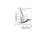
- 4 is a graph of temperature and magnetic field dependence of a resistance value of a channel layer of a strongly correlated nonvolatile memory element in an embodiment of the present invention.
- the trigger layer is a 3 nm thick thin film of Pr 0.5 Sr 0.5 MnO 3
- the tuning layer is a 3 nm thick thin film of Nd 0.5 Sr 0.5 MnO 3 . It is a graph of the electrical resistance in the magnetic sweep after cooling in the magnetic field of the strongly correlated non-volatile memory element in one embodiment of this invention. It is a graph of the electrical resistance in the magnetic sweep after cooling under the magnetic field of the strongly correlated non-volatile memory element in one embodiment of this invention.
- . 4 is a graph of a resistance value of a channel layer with respect to a gate voltage in an example of a strongly correlated nonvolatile memory device according to an embodiment of the present invention. It is a graph which shows the electrical resistance controlled by multiple values by SET operation
- FIG. 1 is a schematic cross-sectional view showing the configuration of a strongly correlated nonvolatile memory element as an example of this embodiment, and the structure of a strongly correlated nonvolatile memory element 100 having a top gate structure (hereinafter referred to as “strongly correlated nonvolatile memory 100”). Indicates.
- a channel layer 2 containing a strongly correlated oxide is formed on the upper surface of the substrate 1 in FIG.
- MOSFETs metal oxide semiconductor field effect transistors
- the inventor of the present application uses, for the channel layer 2, a strongly correlated oxide showing a charge orbital alignment phase or a charge orbital alignment phase in which the charge alignment phase or the orbital alignment phase is established at the same time in the element having the structure exemplified in the strongly correlated nonvolatile memory 100. Therefore, it was noted that switching can be performed by two kinds of physical mechanisms.
- the first physical mechanism for switching is an insulator-metal transition that can be generated in a strongly correlated oxide by an external field that is a perturbation such as a magnetic field, an electric field, an electric current, or light irradiation as described in the background art.
- the second physical mechanism is that an electric field is applied to a channel layer containing a strongly correlated oxide to dope carriers, and the action of the carriers causes a phase transition of the strongly correlated oxide.
- the switching operation of the strongly correlated oxide thin film employed as the channel layer in the present embodiment will be described with reference to FIG. With the structure similar to the field effect element such as the strongly correlated nonvolatile memory 100 in mind, the mechanism of switching and nonvolatile memory function realized in the strongly correlated oxide used for the channel layer will be described.
- FIG. 4A shows a typical magnetic field-temperature electron phase diagram (temperature magnetic field phase diagram) found in a perovskite manganese oxide showing a charge orbital alignment phase.
- a region 402 seen on the low magnetic field side represents a region that becomes an insulator phase generated by charge orbital alignment of strongly correlated oxides.
- a region 404 seen on the high magnetic field side shows a region that becomes a metal phase.
- a region 406 indicated by hatching between these regions indicates a region where the strongly correlated oxide takes a bistable state between the insulator phase and the metal phase by charge orbit alignment.
- the strongly correlated oxide in this region 406 becomes an insulator phase or a metal phase depending on the magnetic field application history. More specifically, when a magnetic field is applied while being fixed at a certain temperature T, the boundary BL starts from the region 402 and becomes a region 406 indicated by hatching. At this point, the strongly correlated oxide is in an insulating state, that is, an insulator phase due to the charge orbit alignment phase. When the magnetic field is increased subsequently, the boundary BH on the high magnetic field side of the region 406 is reached to become the metal phase of the region 404. When passing through this boundary BH, a huge resistance change accompanying switching from the insulator phase to the metal phase is observed in the strongly correlated oxide.
- the strongly correlated oxide metal phase is maintained in the region 404 and the region 406.
- the boundary BL on the low magnetic field side When reaching a certain magnetic field, that is, the boundary BL on the low magnetic field side, the metal phase generated in the strongly correlated oxide disappears.
- the appearance of the bistable state described above is caused by a magnetic field that is an example of the first physical mechanism. Nonvolatility is obtained by this bistable state.
- the boundary BL on the low magnetic field side reaches the temperature axis indicating the magnetic field 0. This indicates that at a temperature lower than this temperature, once the strongly correlated oxide is switched to the metal phase, the metal phase is maintained even after the magnetic field is subsequently removed and does not become an insulator phase.
- FIG. 4B is an explanatory diagram for explaining the carrier doping operation in the perovskite manganese oxide with reference to phase diagrams of temperature and hole amount.
- a phase diagram of an insulator phase and a metal phase there are two ordered phases showing the bistable state of a strongly correlated oxide, that is, a phase diagram of an insulator phase and a metal phase. Taking temperature (absolute temperature).
- the phase boundary BD1 between the insulator phase I and the metal phase M is a so-called double critical state in which two orders compete.
- switching is realized by injecting carriers by an electric field so as to cross the boundary between the insulator phase I and the metal phase M.
- white circles 412 and black circles 414 shown in FIG. 4B indicate a state in which switching is performed from the insulator phase I of the strongly correlated oxide channel layer indicated by the white circle 412 to the metal phase M indicated by the black circle 414. .
- the switching is caused by a decrease in the amount of holes by injecting carriers (electrons in this case) due to the field effect.
- the carrier injection is performed by using an electrode (gate electrode) for forming an electric field with respect to the channel layer and controlling the voltage (gate voltage) to the gate electrode.
- gate electrode an electrode
- the strongly correlated oxide in the channel layer returns to the insulator phase I indicated by the white circle 412 as the amount of holes in the channel layer decreases. For this reason, non-volatility cannot be obtained only by the second physical mechanism.
- FIGS. 4 (a) and 4 (b) the two physical mechanisms for switching shown in FIGS. 4 (a) and 4 (b). That is, when viewed from FIG. 4B, in addition to the temperature and the hole amount, an external field axis corresponding to the horizontal magnetic field in FIG. 4A is introduced.
- the amount of holes is a parameter for controlling the above-described second physical mechanism
- the external field is a parameter for controlling the first physical mechanism.
- the magnetic field shown in FIG. 4A may be used, but control by electric means in the memory element taking the form of a three-terminal element exemplified in the strongly correlated nonvolatile memory 100 is taken into consideration.
- a current flowing directly through the strongly correlated oxide is employed. This current is hereinafter referred to as “source / drain current”.
- FIG. 5 is an explanatory diagram for explaining the role of the source / drain current in particular in relation to the expression of the memory operation realized by the electric means by combining the two physical mechanisms shown in FIG.
- FIG. 5 shows the phase transition of the channel layer 2 in the SET operation with the temperature, hole amount, and current as axes, in particular, the transition between the insulator phase and the metal phase, and the bistable state due to these phases.
- 5A to 5E show (a) gate voltage V g > voltage threshold Vth, source / drain current I sd ⁇ current threshold Ith, and (b) V g > Vth, I sd >, respectively.
- FIG. 5 (a) is the same as FIG. 4 (b), and FIGS. 5 (b) to 5 (d) are phase diagrams showing the strongly correlated oxide in a state where the source / drain current flows.
- FIG. 5E is a phase diagram showing the strongly correlated oxide after the source-drain current is stopped by switching.
- a metal phase region is shown at a position corresponding to the value of the source / drain current.
- the gate voltage Vg is positive so that the carrier to be doped is an electron.
- the metal state is maintained as shown by the black circle 508 in FIG. Is done. This is because the strongly correlated oxide in the state in which the source / drain current flows is in the same bistable state as the region 406 in FIG. Further, even if the current supply is stopped thereafter and the black circle 508 returns to the current axial direction, the metal phase is maintained as indicated by the black circle 510 in FIG.
- the strongly correlated oxide nonvolatile memory element which is one embodiment of the present invention employs a configuration similar to the above-described three-terminal field effect element.
- the operation example described above with reference to FIG. 5 can correspond to an operation for reducing the electrical resistance of the channel layer, that is, a SET operation.
- the nonvolatile memory function can be realized even in the operation of increasing the resistance of the channel layer and returning it to the original state, that is, the RESET operation. Is possible.
- the phase voltage BD2 (FIG. 5 (e)) is set by setting the gate voltage to a voltage having the opposite polarity to the voltage used in the SET operation and then applying the gate voltage. Pass through and switch to insulator phase I (not shown).
- 6 (a) is a timing chart in the case where the source-drain current I s-d, was operated at conditions less than the current threshold value Ith for the SET operation.
- the carrier injection to the application of the gate voltage V g to the switching to the metal phase from the insulator phase As shown in FIG. 4 (b), the carrier injection to the application of the gate voltage V g to the switching to the metal phase from the insulator phase. Accordingly, the source / drain resistance R s-d, that is, the resistance of the strongly correlated oxide in the channel layer becomes a low resistance value R L.
- FIG. 6B is a timing chart showing this operation. As shown in FIG. 6 (b), in this operation, while more than the current threshold Ith that the source drain current I s-d, changing the gate voltage V g to more than Vth. Then the source drain resistance R s-d even if the gate voltage V g below Vth in is maintained at a low resistance value R L.
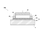
- FIG. 3 is a schematic cross-sectional view showing a configuration of a strongly correlated nonvolatile memory element as an example of the present embodiment, and includes a strongly correlated oxide tuning layer 21 (hereinafter referred to as “tuning layer 21”), and a strongly correlated oxide trigger.
- the structure of a strongly correlated nonvolatile memory element 300 (hereinafter referred to as “strongly correlated nonvolatile memory 300”) having a top gate structure having a channel layer 2 including two layers 22 (“trigger layer 22”) is shown.
- the thin film in order to stabilize the metal phase or realize the metal-insulator transition, the thin film needs to be made thick to some extent. This is because if the thickness of the strongly correlated oxide thin film is too thin, stable metal phase or metal-insulator transition cannot be realized. That is, only in a strongly correlated oxide thin film formed thicker than a critical value related to thickness (hereinafter referred to as “critical thickness”), a metal phase is realized or a metal-insulator transition is realized. In that sense, the critical film thickness can be said to be the lower limit value of the film thickness required for the metal phase to exist stably or for the metal-insulator transition to occur. Due to the phenomenon peculiar to the strongly correlated oxide, even if the channel layer 2 is made thin in order to improve the carrier density, the metal phase or the metal-insulator transition itself may disappear.
- critical thickness a critical value related to thickness
- FIG. 7 is an explanatory diagram for explaining a conduction state in the strongly correlated channel layer 2 having a two-layer structure at each temperature.
- a specific configuration for appropriately setting the thickness of each layer will be described.
- the thickness t1 of the trigger layer 22 of the strongly correlated oxide is made thinner than its critical film thickness t1c
- the thickness t2 of the tuning layer 21 of the strongly correlated oxide is made thinner than its critical film thickness t2c.
- the trigger layer 22 and the tuning layer 21 are single layers, they are thinner than the respective critical film thicknesses t1c and t2c, so that the metal-insulator transition or the metallic phase disappears.
- the inventor of the present application paid attention to the disappearance mechanism because the layer thickness is thin and the electronic state becomes two-dimensional.
- max (t1c, t2c) is a function that returns the maximum value of t1c and t2c that are variables of the function max ().
- this thickness condition is satisfied, first, consider the case where the trigger layer 22 exhibits a metal phase. At this time, the electronic state of the entire channel layer becomes three-dimensional. For this reason, the metal-insulator transition or the metal phase in the entire channel layer 2 is maintained. Next, consider the case where the trigger layer 22 becomes an insulator phase due to metal-insulator transition. At this time, the carrier inside the tuning layer 21 arranged in contact with the trigger layer 22 is not the thickness t of the channel layer 2 as a whole because the trigger layer 22 is an insulator phase, but the tuning of the strongly correlated oxide. Only the thickness t2 of the layer 21 is felt.
- the thickness t2 of the tuning layer 21 is smaller than the critical thickness t2c of the metal phase, the metal phase of the tuning layer 21 disappears, and as a result, the resistance value of the entire channel layer 2 increases.
- the resistance of the entire channel layer is governed by the metal-insulator transition of the trigger layer 22. That is, if the trigger layer 22 is a metal phase, the channel layer 2 is a metal phase having a low resistance value, and if the trigger layer 22 is an insulator phase, the channel layer 2 is an insulator phase having a high resistance value.
- FIGS. 7 in order from (a), in comparison with the track alignment temperature (Orbital ordering temperature) T OO, a temperature higher than the temperature T is T OO (7 (a)), T OO about (FIG. 7 (b)), and is an explanatory view schematically showing the state of movement of the internal conduction carriers in the channel layer 2 in each of a temperature lower than the T OO (Fig 7 (c)).
- T OO 7 (a)
- T OO about FIG. 7 (b)
- FIG. 7 (c) is an explanatory view schematically showing the state of movement of the internal conduction carriers in the channel layer 2 in each of a temperature lower than the T OO (Fig 7 (c)).
- FIG. 7A such as room temperature (300K).
- the strongly correlated oxide trigger layer exhibits a metal phase, the metal phase is maintained.
- T OO a 100K near the trigger layer 22 is a phase transition to the insulator phase of a metal insulator transition (FIG. 7 (b)).
- the conduction carriers in the tuning layer 21 disposed in contact with the trigger layer 22 “feel” only the thickness t 2 of the tuning layer 21. That is, the state of the conductive carrier is affected by a decrease in the thickness of the region where the conductive carrier itself can propagate.
- the thickness for the conductive carrier is not the thickness t of the entire channel layer 2 but the thickness t2 of the tuning layer 21.
- FIG. 7B shows a state in which the conduction carrier conducts only the tuning layer 21 in this state. That is, the conductive carriers in the trigger layer 22 are localized as shown by the white circles in the figure, whereas the conductive carriers in the tuning layer 21 have the channel layer 2 with a thickness of, for example, half. It becomes the same situation as. Thus, the film thickness that can be “feeled” by the conduction carriers in the channel layer 2 is switched from the thickness of the entire channel layer 2 to the thickness of only the tuning layer 21. When further cooled and the temperature falls below TOO , the metal phase of the tuning layer 21 disappears, and as a result, the resistance value of the entire channel layer 2 increases.
- FIG. 7C shows a state where the conductive carriers are localized in any layer in this state.
- FIG. 8 is a schematic diagram showing a mechanism of resistance change of the channel layer by the tuning layer, and the percolation of the metal phase in the tuning layer 21 when the external field strength increases in the order of (a) to (c). It shows the state of.
- a region 82 indicated by diagonal lines is a metal phase
- a white region 84 is an insulator phase.
- a typical channel layer 21 has a thickness of several nm. In this case, it is not necessary to consider the change in the film thickness direction, and the domain is considered to be uniform in the film thickness direction.
- the resistance is high when the region of the insulator phase is large. Then, when the external field strength such as the above-described source / drain current is increased, the insulator phase region 82 is reduced as shown in FIG. 8B, and the metal phase region 84 occupies that much. Will increase. When the external field strength is further increased, the insulator phase region 84 is hardly seen as shown in FIG.
- the ratio of the metal phase to the insulator phase in the tuning layer 21 changes according to the external field strength, and the degree of carrier localization also changes according to the state of the percolation path.
- the value of the electrical resistance of the tuning layer 21 can be realized not only as a binary value of low resistance and high resistance but as a value of 3 or more.
- the resistance value of the tuning layer 21 is determined by the geometrical structure (length, thickness, number) of the path by percolation between the source and drain. For this reason, the resistance value of the channel layer 2 as a whole can take a value of three or more according to the state of the tuning layer 21, that is, it can be multivalued.
- the switching operation is realized by an insulator-metal transition in the trigger layer 22. Further, by using percolation generated in the metal phase region 82 and the insulator phase region 84 in the tuning layer 21, the resistance value can be multivalued.
- the strongly correlated nonvolatile memory 100 is manufactured in a top gate structure.
- a gate electrode 41 is formed on the upper surface of the channel layer 2 in FIG.
- a drain electrode 42 and a source electrode 43 are formed so as to be in contact with the channel layer 2.
- the channel layer 2 can be grown epitaxially on the substrate 1. Thereby, a high-quality thin film can be produced as the channel layer 2.
- the substrate 1 is preferably (LaAlO 3 ) 0.3 (SrAl 0.5 Ta 0.5 O 3 ) 0.7 (hereinafter abbreviated as LSAT) or SrTiO 3 .
- LSAT laAlO 3
- the channel layer can be a perovskite-type manganese oxide capable of phase transition between the metal phase and the insulator phase that is either the charge alignment phase or the orbital alignment phase.
- a strongly correlated nonvolatile memory element having a bottom gate structure can be manufactured.
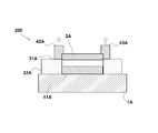
- 2 is a schematic cross-sectional view of a strongly correlated nonvolatile memory element 200 (hereinafter referred to as “strongly correlated nonvolatile memory 200”) having a bottom gate structure, which is another example of the strongly correlated nonvolatile memory element of the present embodiment.
- the gate electrode 41A is disposed on the substrate 1A side as viewed from the channel layer 2.
- the substrate A gate electrode 41A is formed as a conductive oxide thin film that can be epitaxially grown on the upper surface of FIG. 2 of FIG. 1A, and then a gate insulator 31A and a channel layer 2A of a strongly correlated oxide are stacked in this order.
- the gate electrode 41A, the gate insulator 31A, and the channel layer 2A are first formed with these three layers. Thereafter, the three layers are collectively etched by photolithography to pattern the in-plane shape of the substrate 1A and processed as shown in FIG. Then, after forming the insulating film 32A, the drain electrode 42A and the source electrode 43A are formed at any position in contact with the surface or interface of the channel layer 2. Thus, the structure of the strongly correlated nonvolatile memory 200 of FIG. 2 is formed.
- a channel layer 2 including a tuning layer 21 and a trigger layer 22 in this order from the substrate 1 side is formed on the upper surface of the substrate 1 in FIG.
- a gate electrode 41 is formed on the upper surface of the channel layer 2 in FIG. Further, a drain electrode 42 and a source electrode 43 are formed so as to be in contact with the channel layer 2. In FIG. 3, a drain electrode 42 and a source electrode 43 in contact with the trigger layer 22 are illustrated as an example. Then, by selecting a perovskite oxide as a material constituting the substrate 1 and the two layers (the tuning layer 21 and the trigger layer 22) included in the channel layer 2, the tuning layer 21 and the trigger layer 22 of the channel layer 2 are selected. Can be epitaxially grown on the substrate 1. Thereby, a high-quality thin film can be produced as the channel layer 2.
- the tuning layer 21 in the strongly correlated nonvolatile memory 300 shown in FIG. 3 will be described.
- the tuning layer 21 preferably employs an Nd 0.5 Sr 0.5 MnO 3 thin film when the substrate 1 is LSAT, and the substrate 1 is SrTiO 3. In the case of 3 , it is preferable to employ a Pr 0.5 Sr 0.5 MnO 3 thin film.
- the trigger layer 22 will be described.
- the trigger layer 22 is also preferably a Pr 0.5 Sr 0.5 MnO 3 thin film when the substrate 1 is LSAT, and the substrate 1 is SrTiO 3 . It is preferable to employ a Nd 0.5 Sr 0.5 MnO 3 thin film.
- the gate insulator 31, the gate electrode 41, the drain electrode 42, and the source electrode 43 do not need to be perovskite oxides, and a material that can be used can be selected as appropriate.
- the selected material are Pr 0.5 Sr 0.5 MnO 3 and Nd 0.5 Sr 0.5 MnO 3 when the substrate 1 is LSAT.
- the material examples are Nd 0.5 Sr 0.5 MnO 3 and Pr 0.5 Sr 0.5 MnO 3 , respectively.
- the materials employed in the strongly correlated nonvolatile memory element as an example of the present embodiment are Pr 0.5 Sr 0.5 MnO 3 as the trigger layer 22 and Nd 0.5 Sr 0.5 MnO 3 as the tuning layer 21.
- the substrate 1 is an LSAT (110) plane orientation substrate. None of the configuration of the manufacturing apparatus is illustrated.
- the channel layer 2 including a strongly correlated oxide thin film was produced using a laser ablation method.
- a polycrystalline material having each composition produced by forming into a cylindrical shape of ⁇ 20 mm ⁇ 5 mm by a solid phase reaction method was used as the target of each material.
- the vacuum chamber in which the LSAT (110) substrate was attached as the substrate 1 was evacuated to 3 ⁇ 10 ⁇ 9 Torr (4 ⁇ 10 ⁇ 7 Pa) or less. Thereafter, high purity oxygen gas was introduced at 1 mTorr (0.133 Pa), and the substrate was heated until it reached 900 ° C.
- the target was irradiated with a KrF excimer laser having a wavelength of 248 nm through the laser beam introduction port of the chamber.
- an Nd 0.5 Sr 0.5 MnO 3 thin film having a thickness of 11 atomic layers was formed as the tuning layer 21.
- a Pr 0.5 Sr 0.5 MnO 3 thin film having a thickness of 11 atomic layers was formed as a strongly correlated oxide layer for the trigger layer 22 in the same atmosphere.
- the thickness of one atomic layer corresponds to the interval (110) of the (110) plane.
- the thickness t1 of the strongly correlated oxide trigger layer 22 is 3 nm
- the thickness t2 of the tuning layer 21 is 3 nm
- the thickness t of the channel layer 2 is 6 nm.
- alumina oxide was formed as the gate insulator 31 by atomic layer deposition. Thereafter, a three-terminal strongly correlated non-volatile memory element shown in FIG. 1 was fabricated through photolithography, etching, and electrode fabrication processes.
- FIG. 9 is a graph of the temperature dependence of the volume resistivity ⁇ of each material.
- FIG. 9A is for Nd 0.5 Sr 0.5 MnO 3
- FIG. 9B is for Pr 0.5 Sr 0.5 MnO 3 .
- Each graph shows an external magnetic field as a parameter. As shown in FIG.
- the Pr 0.5 Sr 0.5 MnO 3 thin film exhibits sharp metal-insulator transition due to orbital order on the LSAT (110) substrate.
- the critical film thickness t1c in Pr 0.5 Sr 0.5 MnO 3 is about 5 nm.
- the Nd 0.5 Sr 0.5 MnO 3 thin film (film thickness is 80 nm) has a charge orbit alignment insulator phase and a metal phase on the LSAT (110) substrate as shown in the graph of FIG. Shows a two-phase coexistence state.
- FIG. 10 is a graph obtained by measuring the electrical resistance of the channel layer 2 of the strongly correlated nonvolatile memory 300 manufactured by the above-described process while changing the temperature and the magnetic field.
- the magnetic field which is one of the external fields having the same action as the gate voltage, is applied while keeping the gate voltage at 0V.
- the electrical resistance of the channel layer 2 increases rapidly at 100K, and the ratio of electrical resistance before and after the increase is 6 at the maximum. We confirmed that it could be more than digits.
- the channel layer 2 including the strongly correlated oxide trigger layer 22 and the strongly correlated oxide tuning layer 21 can be in an insulating state by metal-insulator transition in the strongly correlated oxide forming the trigger layer 22. is there.
- the metal phase of the tuning layer 21 disappears due to the influence of the metal-insulator transition in the strongly correlated oxide of the trigger layer 22.
- the resistance value changed according to the magnetic field strength. This indicates that the percolation path is generated between the electrodes by increasing the metal phase in the tuning layer 21 as the magnetic field strength increases. That is, the resistance value of the entire channel layer 2 is switched by the trigger layer 22 and the resistance value takes a value of three or more according to the percolation path in the tuning layer 21.
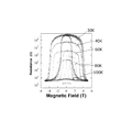
- FIG. 11 is a graph of the electric resistance of the strongly correlated nonvolatile memory 300 after cooling in the absence of a magnetic field.
- Each curve is a magnetic field at each temperature of 30K, 40K, 60K, 80K, and 100K in order from the side with the largest resistance change.
- the horizontal axis represents the sweep magnetic field indicated by the unit of magnetic flux density. At each temperature, it was confirmed that a bistable state was realized as in the temperature magnetic field phase diagram shown in FIG.
- the low resistance state that is, the metal phase generated by applying the 5T sweep magnetic field is substantially maintained even in the absence of a magnetic field. For this reason, it is fully conceivable that the metal phase can be maintained even in the absence of a magnetic field if the magnetic field strength is larger even at a temperature other than 100K.
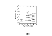
- FIG. 12 is a graph of electric resistance after cooling the strongly correlated nonvolatile memory 300 under a magnetic field. Each curve is a result obtained by performing a magnetic field sweep after applying a magnetic field cooling process in which 1.05T, 1.1T, 1.3T, 1.5T, and 2T magnetic fields (initial magnetic fields) are applied in order from the higher resistance side. Yes, the horizontal axis indicates the swept magnetic field in units of magnetic flux density.
- Each curve is obtained when the initial magnetic field is used as a starting point and the magnetic field is swept up to the opposite magnetic field with the same strength as the initial magnetic field and then returned to the initial magnetic field.
- the initial magnetic field is 1.05 T
- the electrical resistance increases when no magnetic field is applied, and a substantially constant value is maintained at the high electrical resistance in the subsequent magnetic field sweep. This is considered to correspond to the change of the percolation path.
- the initial magnetic field exceeds 1.05T, the resistance value decreases as the strength of the initial magnetic field increases, and any of the initial magnetic fields of 1.1T, 1.3T, 1.5T, and 2T In this case, the resistance value in the absence of a magnetic field at the time of sweep is kept almost constant. From this, it can be seen that the phase state that realizes a resistance value of three or more according to the percolation path in the tuning layer 21 is stable.
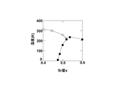
- the vertical axis in FIG. 13 is the temperature (K), and the horizontal axis is the Sr amount, that is, the hole doping amount x.
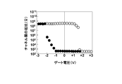
- FIG. 14 is a graph of the resistance value of the channel layer against the gate voltage in the embodiment of the strongly correlated nonvolatile memory 300.
- White circles and black circles indicate measured values of electrical resistance values when the gate voltage is increased to the positive polarity side (first polarity) and when the gate voltage is decreased to the negative polarity side (second polarity), respectively.
- the gate voltage is the potential of the gate electrode 41 when the source electrode 43 is based on 0V.
- the gate voltage is set and the electric resistance value between the source electrode 43 and the drain electrode 42 is measured, and the electric resistance value is shown as the resistance of the channel layer 2. Further, the measurement was performed by cooling the strongly correlated nonvolatile memory 300 to 30K.
- the absolute value was increased by increasing the gate voltage to the positive polarity side as shown in the characteristics of FIG. Then, a step-like behavior having a threshold value that the electric resistance value of the channel layer rapidly decreases in the vicinity of about 1.8 V was confirmed. Further, when the gate voltage was applied up to +3 V, the electrical resistance value of the channel layer showed a change of 5 digits or more from the state where the gate voltage was not applied.
- This operation is a SET operation in which the channel layer 2 is transitioned to a low resistance state (SET state) by making a metal phase.
- the gate voltage was applied to the negative polarity side. Then, as shown in FIG. 14, an increase in resistance value was observed after ⁇ 1V.
- the voltage was further applied to the negative side and the absolute value of the voltage was increased while maintaining the negative polarity, it returned to the initial high resistance state (OFF state) at ⁇ 2 V or more.
- This operation is a RESET operation in which the channel layer 2 is changed to the high resistance state (OFF state) by setting the channel layer 2 to the insulator phase. At that time, it was confirmed that a gentle behavior with a threshold value of -1 V and a high resistance state by the RESET operation were obtained.
- the SET operation and the RESET operation can be performed, and the low resistance state (SET state) and the high resistance state (OFF state) can be transited to each other. Met. Further, it was confirmed that in both the SET state and the OFF state, a nonvolatile memory function in which each state is maintained in a state where the gate voltage is 0 V and no current flows through the channel layer was confirmed.
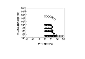
- FIG. 15 is a graph showing electrical resistance controlled to multiple values by the SET operation of the strongly correlated nonvolatile memory element 300.
- the gate voltage is lowered to 0 V which is lower than the threshold voltage of +1.8 V while supplying the source / drain currents of the above values. I let you. And after the voltage drop, the electrical resistance of the channel layer was measured.
- the resistance value of the channel layer changed at the time when the gate voltage was 0 V in accordance with each value of the source / drain current value.
- the resistance value of the channel layer changed to about 10 4 ⁇ , about 10 5 ⁇ , and about 10 6 ⁇ depending on the source / drain currents of 80 ⁇ A, 70 ⁇ A, and 60 ⁇ A, respectively. .
- These resistance values were maintained even when the source / drain current value was 0 A at that time.
- multi-value resistance control in which the resistance value of the channel layer is controlled to each value in the state where the gate voltage is 0 V is realized.
- the threshold current of the source / drain current was in the range of 40 ⁇ A or more and less than 60 ⁇ A. As described above, it was confirmed that a non-volatile memory function capable of performing a multi-value storing operation was developed.
- the physical mechanism of the non-volatile memory function of such multi-value storage operation is realized by making use of the characteristics of the above strongly correlated oxide thin film with the carrier amount as the Sr amount and the external field as the magnetic field. It is.
- the amount of carriers injected into the channel layer is controlled by the gate voltage. That is, the control as if the Sr amount was controlled in FIG. 13 was realized by the voltage applied to the gate electrode, and the control corresponding to the lateral movement in the electronic phase diagram of FIG. 4B or FIG. 5 was performed. Was confirmed.
- the phenomenon similar to the behavior of FIGS. 9 to 12 described based on the magnetic field as the external field is realized in the strongly correlated nonvolatile memory 300 by the source / drain current.
- the value of the source / drain current can be regarded as a kind of the external field having an action of maintaining the strongly correlated oxide thin film in the metal phase.
- the current value is clearly shown as an additional axial movement.
- the inventor of the present application indicates that the percolation described with reference to FIGS. 11 and 12 is likely to hold in the same manner even when the source / drain current acts as an external field. thinking. That is, a multi-level stable state is realized due to the formation state of the percolation path in the tuning layer controlled by the value of the source / drain current. And since it is possible to achieve both the above-described non-volatility and control of the source / drain current, it is considered that a multi-value non-volatile effect appears. Since the nonvolatile memory function controlled by such electrical means originates from the phase transition phenomenon of the strongly correlated electron system in the first place, the strong correlation employed as the material of the channel layer in this embodiment is used.
- FIG. 16 is a graph showing electrical resistance controlled to multiple values by the RESET operation of the strongly correlated nonvolatile memory element 300. For this measurement, first, set the gate voltage to 0 while flowing a current of 100 ⁇ A between the source and drain, once complete the SET operation, and then apply the gate voltage further to the negative side to determine the absolute value of the gate voltage. Increased.
- the ultimate voltage of the source and drain voltages is set to -1V, -1.25V, -1.5V, and -1.75V, and then the electrical resistance is measured until the gate voltage is raised to zero. did.
- the electrical resistance of the channel layer was maintained at a resistance value corresponding to the ultimate voltage value of the negative side gate. That is, by adjusting the absolute value of the gate voltage in a voltage range that is equal to or higher than the threshold voltage (1 V), the absolute value of the gate voltage is lowered below the threshold voltage or the resistance value of the channel layer after the application is stopped. Was confirmed to be controlled to 3 values or more. It was confirmed that the multi-value nonvolatile memory function corresponding to the applied voltage value as the reached voltage in the OFF state was realized by operating in this way.
- the multi-value storage operation by the RESET operation also has an advantage that the above-described control by the source / drain current as an external field is not required except for the SET operation performed first. Therefore, in the RESET operation, by adjusting the applied voltage value through the gate electrode 41, the resistance value of the channel layer 2 after stopping the application of the gate voltage is set to three or more without using the control of the source / drain current value. It is possible to control.
- the description of the present embodiment based on the above-described example is based on the strongly correlated nonvolatile memory 300 in which the trigger layer 22 and the tuning layer 21 are adopted as the channel layer 2.
- the configuration of the strongly correlated memory element according to the present embodiment is not necessarily limited to the configuration of the channel layer having such a configuration, and includes a strongly correlated memory element having an arbitrary specific structure that satisfies the detailed operation principle. It is a waste.
- the bistability described with reference to FIG. 4A is established even when a single channel layer is employed.
- the strongly correlated nonvolatile memories 100 and 200 described with reference to FIGS. 1 and 2 also exhibit a nonvolatile memory function originating from bistability, and more than three values originating from percolation. Value storage can be realized.
- the configuration of the channel layer 2 including the two layers of the tuning layer 21 and the trigger layer 22 has been described by taking only the top gate strongly correlated nonvolatile memory 300 (FIG. 3) as an example. This is because, in the strongly correlated nonvolatile memory 100 (FIG. 1), the channel layer 2 is formed by the first strongly correlated oxide trigger layer 22 and the second strongly correlated oxide tuning layer, and the gate insulation. The body 31 is configured to be sandwiched between the trigger layer 22 and the gate electrode 41. However, the channel layer 2 including two layers of the tuning layer 21 and the trigger layer 22 can also be employed in the strongly correlated nonvolatile memory 200 (FIG. 2) having a bottom gate configuration.
- the channel layer 2 is formed of the first type strongly correlated oxide trigger layer 22 and the second type strongly correlated oxide tuning layer, and the gate insulator 31 is formed with the trigger layer 22. It is also possible to configure so as to be sandwiched between the gate electrodes 41. In both the top gate configuration and the bottom gate configuration, the channel layer 2 can be controlled through the control of the trigger layer 22.
- the (110) plane orientation substrate is used.
- the single crystal thin film on the (210) plane orientation substrate can also undergo primary transition, the same applies to the case of using the (210) plane orientation substrate. It is possible to realize a strongly correlated oxide field effect element exhibiting a huge resistance change. Note that the materials, compositions, film thicknesses, formation methods, and the like of the thin film and the substrate exemplified in this embodiment are not limited to the above embodiments.
- the strongly correlated nonvolatile memory of the present invention can be used in any electrical / electronic device that uses an element that exhibits a nonvolatile switching function by electrical means.
Landscapes
- Engineering & Computer Science (AREA)
- Chemical & Material Sciences (AREA)
- Materials Engineering (AREA)
- Computer Hardware Design (AREA)
- Crystallography & Structural Chemistry (AREA)
- Semiconductor Memories (AREA)
- Mram Or Spin Memory Techniques (AREA)
- Hall/Mr Elements (AREA)
Abstract
Description
t=t1+t2≧max(t1c,t2c)
ただし、
t1<t1c、t2<t2c、max()は変数群の最大値を返す関数、なる関係を満たしていることが好ましい。
[1 動作原理]
[1-1 メモリー素子の概略構成]
図1は、本実施形態の一例の強相関不揮発メモリー素子の構成を示す概略断面図であり、トップゲート構造を有する強相関不揮発メモリー素子100(以下「強相関不揮発メモリー100」と記す)の構造を示す。図1における基板1の紙面の上方の面の上には強相関酸化物を含むチャネル層2が形成されている。なお、本出願全般において、トップゲート構造やチャネル層との用語を含むその他の用語は、従来の電界効果素子の代表的な構成である例えばシリコン用いるMOSFET(金属酸化物半導体電界効果トランジスター)と対比することにより、本願の説明の理解を容易にするためのみに記載されている。
本願の発明者は、強相関不揮発メモリー100に例示される構造の素子において、電荷整列相や軌道整列相あるいは両方が同時に成立する電荷軌道整列相を示す強相関酸化物をチャネル層2に用いることにより、2種類の物理的機構でスイッチングを行なわせうることに着目した。スイッチングのための第1の物理的機構は、背景技術で記載したように磁場、電場、電流、光照射などの摂動となる外場により強相関酸化物に生じさせうる絶縁体金属転移である。また、第2の物理的機構は、強相関酸化物を含むチャネル層内に電界を作用させてキャリアをドーピングし、そのキャリアの作用によって強相関酸化物の相転移を引き起こす、というものである。
第1の物理的機構を説明するために、図4(a)に、電荷軌道整列相を示すペロフスカイトマンガン酸化物に見られる典型的な磁場-温度電子相図(温度磁場相図)を示す。低磁場側に見られる領域402は強相関酸化物が電荷軌道整列することによって生じる絶縁体相となる領域を表している。これに対し、高磁場側に見られる領域404は金属相となる領域を示している。そして、これらに挟まれたハッチングで示す領域406は、強相関酸化物が電荷軌道整列による絶縁体相と金属相との間で双安定状態をとる領域を示している。すなわち、この領域406における強相関酸化物は、磁場印加履歴に応じて絶縁体相であったり金属相となったりする。より具体的には、ある温度Tに固定したまま磁場を印加してゆくと、領域402から出発して境界BLを過ぎ、ハッチングで示す領域406となる。この時点での強相関酸化物は電荷軌道整列相による絶縁状態すなわち絶縁体相となっている。続けて磁場を増大させると、領域406の高磁場側の境界BHに達して領域404の金属相となる。この境界BHを通過する際に、強相関酸化物には、それまでの絶縁体相から金属相へとスイッチングすることに伴う巨大な抵抗変化が観察される。逆に、同一温度で磁場を減少させていくと、領域404および領域406において強相関酸化物の金属相が維持される。そして、ある磁場つまり低磁場側の境界BLに達すると、強相関酸化物に生じていた金属相は消失してゆく。以上に述べた双安定状態の出現は、第1の物理的機構の一例である磁場によってもたらされている。この双安定状態により不揮発性が得られる。なお、図4(a)の温度磁場相図において、この低磁場側の境界BLが磁場0を示す温度軸に到達している。このことは、この温度より低温では、強相関酸化物が一旦、金属相へとスイッチングすると、その後に磁場をとりさった後でも金属相が維持され、絶縁体相とならないことを示している。
ここで、本願の発明者は、図4(a)および(b)に示したスイッチングのための二つの物理的機構を組み合わせることによって、不揮発性メモリーの動作が可能であることに気づいた。すなわち、図4(b)から見ると、温度とホール量に加え、図4(a)の横軸の磁場に相当する外場の軸を導入する。ホール量が上述した第2の物理的機構を制御するパラメータであり、外場が第1の物理的機構を制御するパラメータである。そしてその外場としては、図4(a)に示した磁場であってもよいが、強相関不揮発メモリー100に例示される3端子素子の形態をとるメモリー素子における電気的手段による制御を念頭におき、ここでは強相関酸化物に直接流す電流を採用する。この電流を以下「ソースドレイン電流」と呼ぶ。
次に、チャネル層2としてトリガー層とチューニング層の積層構造を採用する場合の強相関酸化物の転移現象について説明する。図3は、本実施形態の一例の強相関不揮発メモリー素子の構成を示す概略断面図であり、強相関酸化物のチューニング層21(以下、「チューニング層21」という)、強相関酸化物のトリガー層22(「トリガー層22」)の2層を備えるチャネル層2を有するトップゲート構造の強相関不揮発メモリー素子300(以下「強相関不揮発メモリー300」と記す)の構造を示す。一般に、強相関酸化物薄膜において、金属相を安定させたり、金属絶縁体転移が実現したりするためには、その薄膜はある程度厚く作製されている必要がある。強相関酸化物薄膜の膜厚があまりに薄いと安定した金属相や金属絶縁体転移が実現しないためである。すなわち、厚みに関する臨界値(以下「臨界膜厚(critical thickness)」という)より厚く形成されている強相関酸化物薄膜においてのみ、金属相が実現したり、金属絶縁体転移が実現したりする。その意味において、臨界膜厚とは、上記の金属相が安定に存在するため、または、金属絶縁体転移が発現するために必要となる膜厚の下限値ともいえる。この強相関酸化物特有の現象のために、キャリア密度の向上を狙ってチャネル層2を薄くしていっても、金属相や金属絶縁体転移自体が消失する場合がある。
続いてチューニング層内の金属相のパーコレーションについて図8に基づいて説明する。図8は、チューニング層によるチャネル層の抵抗変化のメカニズムを示す模式図であり、(a)から(c)の順に、外場強度が増大していった際のチューニング層21における金属相のパーコレーションの様子を示したものである。図中、斜線により示した領域82が金属相であり、白い領域84が絶縁体相を示している。本実施形態においては、典型的なチャネル層21の厚みは数nmとする。この場合、膜厚方向の変化は考慮する必要が無く、ドメインは膜厚方向に一様であると考えられる。まず、図8(a)に示すように絶縁体相の領域が大きい状態では抵抗は高い。そこから、上述したソースドレイン電流などのような外場強度を増加させると、図8(b)に示すように絶縁体相の領域82が縮小し、その分だけ金属相の領域84が占める割合が増加する。さらに外場強度を増加すると、図8(c)に示すように絶縁体相の領域84は殆どみられなくなる。
以下、本実施形態の強相関酸化物を用いる強相関不揮発メモリー素子を図面に基づいて説明する。本実施形態の強相関不揮発メモリー素子の構造を、典型的な二つの構成すなわちトップゲート構成とボトムゲート構成について説明する。さらに、チャネル層を2層の積層構造とする好ましい構造についても説明する。
再び図1を参照して、本実施形態の一例の強相関不揮発メモリー素子の構成について説明する。概略断面図として示されるように、強相関不揮発メモリー100はトップゲート構造に作製されている。チャネル層2の図1における上面には、ゲート絶縁体31を介してゲート電極41が形成されている。さらに、チャネル層2に接するように、ドレイン電極42およびソース電極43が形成されている。そして、基板1とチャネル層2とを構成する物質としてペロフスカイト型酸化物を選択することにより、チャネル層2を、基板1に対してエピタキシャルに成長させることが可能となる。これにより、チャネル層2として高品質な薄膜を作製することが可能となる。例えば、基板1としては(LaAlO3)0.3(SrAl0.5Ta0.5O3)0.7(以下、LSATと略記する)あるいはSrTiO3が好ましい。このように構成することにより、チャネル層を、金属相と、電荷整列相または軌道整列相のいずれかである絶縁体相との間において相転移可能なペロフスカイト型マンガン酸化物とすることができる。
図1に示した強相関不揮発メモリー100の変形として、本実施形態においては、ボトムゲート構造の強相関不揮発メモリー素子を作製することも可能である。図2は、本実施形態の強相関不揮発メモリー素子の別の例であるボトムゲート構造の強相関不揮発メモリー素子200((以下「強相関不揮発メモリー200」と記す)の概略断面図である。図2に示したように、強相関不揮発メモリー200においては、チャネル層2からみて基板1A側にゲート電極41Aが配置されている。この構造の電界効果素子200を作製するためには、まず、基板1Aの図2における紙面の上方の面の上に、エピタキシャル成長可能な導電性の酸化物薄膜としてゲート電極41Aを形成し、次いでゲート絶縁体31A、強相関酸化物のチャネル層2Aを、この順に積層する。これらの基板1Aと、チャネル層2Aと、チャネル層2Aおよび基板1Aの間に位置するゲート電極41Aおよびゲート絶縁体31Aとのすべてが、ペロフスカイト型酸化物により構成されていることにより、チャネル層2Aとして、基板1Aに対してエピタキシャルに成長する高品質な薄膜を作製することが可能となる。例えば、基板1AとしてはLSATあるいはSrTiO3が望ましい。ゲート電極41AとしてはLa1-xSrxMnO3薄膜(x=0.2~0.4)、ゲート絶縁体31Aとしては基板1Aと同種の物質、すなわち基板1AがLSATの場合はLSAT、基板1AがSrTiO3の場合はSrTiO3を選択することが好ましい。また、強相関酸化物のチャネル層2Aとしては基板1AがLSATである場合には、例えばPr0.5Sr0.5MnO3薄膜とすることが好ましく、また、基板1AがSrTiO3である場合には、Nd0.5Sr0.5MnO3薄膜とすることが好ましい。このように構成することにより、チャネル層を、金属相と、電荷整列相または軌道整列相のいずれかである絶縁体相との間において相転移可能なペロフスカイト型マンガン酸化物とすることができる。
再び図3を参照して、トップゲート構成の強相関不揮発メモリー素子300の構造について説明する。図3における基板1の紙面の上方の面の上には、チューニング層21と、トリガー層22とを、基板1側からこの順に含むチャネル層2が形成されている。
[3-1 素子作製例]
以下、本実施形態の強相関不揮発メモリー素子の作製方法を説明する。この説明は、図3に示した、チューニング層21、トリガー層22の2層を備えるチャネル層2を有するトップゲート構造の強相関不揮発メモリー300の一例の実施例を作製した具体的方法に基づくものである。以下に実施例を挙げて本発明をさらに具体的に説明する。以下の実施例に示す材料、使用量、割合、処理内容、処理手順等は本発明の趣旨を逸脱しない限り適宜変更することかできる。したがって、本発明の範囲は以下の具体例に限定されるものではない。
[3-2-1 磁場を外場とする場合の特性]
次に、上記実施例のチューニング層21として採用したNd0.5Sr0.5MnO3と、トリガー層22として採用したPr0.5Sr0.5MnO3とのより一般的な特性について説明する。図9は、各材料の体積抵抗率ρの温度依存性のグラフである。図9(a)は、Nd0.5Sr0.5MnO3、そして図9(b)はPr0.5Sr0.5MnO3のものである。各グラフは、外部磁場をパラメータとして示している。図9(b)に示すように、Pr0.5Sr0.5MnO3薄膜(膜厚は40nm)はLSAT(110)基板上においては軌道秩序によるシャープな金属絶縁体転移を示す。別途検討したところ、Pr0.5Sr0.5MnO3における臨界膜厚t1cは約5nmである。これに対し、Nd0.5Sr0.5MnO3薄膜(膜厚は80nm)は図9(a)のグラフに示すようにLSAT(110)基板上においては電荷軌道整列絶縁体相と金属相が混じった二相共存状態を示す。Nd0.5Sr0.5MnO3の臨界膜厚t2cは約5nm未満である。したがって、上記実施例におけるチャネル層2は、t=t1+t2≧max(t1c、t2c)、ただしt1<t1c、t2<t2cの条件を満たしている。
[3-2-2-1 チャネル層の磁場による相転移]
次に、強相関不揮発メモリー300の特性について説明する。図10は、上述した工程により作製した強相関不揮発メモリー300のチャネル層2の電気抵抗を、温度および磁場を変えながら測定したグラフである。ここでは、ゲート電圧を0Vに保ち、ゲート電圧と同様の作用を及ぼす外場の一つである磁場を印加している。図10に示すように、強相関不揮発メモリー300の温度を室温から冷却していくと、チャネル層2の電気抵抗が100Kにおいて急激に増大し、その増大前後での電気抵抗の比率は最大で6桁以上となりうることを確認した。すなわち、強相関酸化物のトリガー層22と強相関酸化物のチューニング層21を備えるチャネル層2は、トリガー層22をなす強相関酸化物における金属絶縁体転移により、絶縁状態とすることが可能である。このように、強相関酸化物のチューニング層21が存在しているにもかかわらず、トリガー層22の強相関酸化物における金属絶縁体転移の影響によってチューニング層21の金属相は消失している。このため、チャネル層2全体としてみても巨大な抵抗変化が得られることが確認された。さらに、磁場を印加し冷却すると磁場強度に応じて抵抗値が変化することを確認した。これはチューニング層21中の金属相が、磁場強度の増大に応じて増加することでパーコレーション経路が電極間で発生していることを示している。すなわちチャネル層2全体の抵抗値はトリガー層22によりスイッチングし、なおかつ、チューニング層21中のパーコレーション経路に応じてその抵抗値は3値以上の値をとるのである。
強相関不揮発メモリー300においてさらに無磁場下で所定の温度に冷却し、その後に磁場を掃引して印加しチャネル層2の電気抵抗を測定した。図11は、強相関不揮発メモリー300の無磁場下冷却後の電気抵抗のグラフであり、各曲線は、抵抗変化の大きい側から順に、30K、40K、60K、80K、および100Kの各温度で磁場を掃引して測定した結果であり、横軸は磁束密度の単位により示す掃引磁場である。各温度において、図4(a)に示した温度磁場相図のように双安定状態が実現することが確認された。特に100Kでは、5Tの掃引磁場の印加により生じた低抵抗状態すなわち金属相が無磁場下でもほぼ保たれている。このため、100K以外の温度においても磁場強度がより大きければ同様に金属相が無磁場下でも保たれることも十分考えられる。
また、外場によるパーコレーション状態の変化を調べるために300Kにて磁場を印加した後、5Kまで冷却し測定した磁場冷却(Field Cooling)処理における電気抵抗を調べた。図12は、強相関不揮発メモリー300の磁場下冷却後の電気抵抗のグラフである。各曲線は、抵抗の高い側から順に1.05T、1.1T、1.3T、1.5T、および2Tの磁場(初期磁場)を印加する磁場冷却処理後に磁場掃引を行なって測定した結果であり、横軸はその掃引された磁場を磁束密度の単位により示している。また、各曲線は初期磁場を出発点にして、初期磁場と同じ強度で逆向きの磁場まで磁場を掃引し、再び初期磁場に戻すような磁場履歴を経た場合のものである。初期磁場を1.05Tとした場合は、無磁場下になると電気抵抗が高くなり、その後の磁場掃引において、その高い電気抵抗にてほぼ一定の値を保っている。これはパーコレーション経路の変化に対応しているものと考えられる。初期磁場が1.05Tを超える場合には、初期磁場の強度を増大させるのに応じて抵抗値は低くなり、1.1T、1.3T、1.5T、および2Tのうちのいずれの初期磁場の場合も、掃引時の無磁場下における抵抗値がほぼ一定に保たれる。このことから、チューニング層21におけるパーコレーション経路に応じた3値以上の抵抗値を実現する相状態は安定であることがわかる。
[3-3-1 不揮発性メモリー機能]
続いて、電界効果による抵抗変化および不揮発性メモリー機能について説明する。図14は、強相関不揮発メモリー300の実施例においてゲート電圧に対するチャネル層の抵抗値のグラフである。白丸および黒丸は、それぞれ、ゲート電圧を正極性側(第1極性)に上昇させてゆく場合、および負極性側(第2極性)に低下させてゆく場合についての電気抵抗値の測定値を示している。なお、ゲート電圧は、ソース電極43を0Vの基準とした場合のゲート電極41の電位である。また、この測定においては、ゲート電圧を設定してソース電極43とドレイン電極42の間の電気抵抗値を測定し、その電気抵抗値をチャネル層2の抵抗として図示している。さらに測定は、強相関不揮発メモリー300を30Kに冷却して行なった。
[3-3-2-1 SET動作における多値メモリー動作]
さらに、図14と同様の動作条件において、ソース、ドレイン間に流す電流値(ソースドレイン電流値)のみ80μA、70μA、60μA、と変え同様の測定を行なった。図15は、強相関不揮発メモリー素子300のSET動作により多値に制御される電気抵抗を示すグラフである。この測定のためには、まず上記SET動作の途中の+3Vのゲート電圧を印加した状態において、上記各値のソースドレイン電流を流しながらゲート電圧を、+1.8Vの閾値電圧を下回る0Vへと低下させた。そしその電圧低下の後に、チャネル層の電気抵抗を測定した。その結果、図15に示すように、ソースドレイン電流値の各値に応じ、ゲート電圧が0Vの時点におけるチャネル層の抵抗値が変化することが観察された。具体的な数値に基づいて説明すると、80μA、70μA、60μAのそれぞれの値のソースドレイン電流に応じて、チャネル層の抵抗値が約104Ω、約105Ω、約106Ωと変化した。そして、これらの抵抗値はその時点でソースドレイン電流の値を0Aとしても維持された。このように、ゲート電圧を0Vとした状態において、チャネル層の抵抗値がそれぞれの値に制御される、多値の抵抗値制御が実現されることを確認した。なお、ソースドレイン電流値を40μA未満とした場合には、チャネル層の抵抗値は約108Ω程度となり、チャネル層の抵抗値の制御を行なうことはできなかった。このため、ソースドレイン電流の閾値電流は、40μA以上60μA未満の範囲にあったものと推測している。以上のようにして、多値の記憶動作を行ないうる不揮発性メモリー機能が発現することを確認した。
多値の不揮発性メモリー機能を実現する別の方法としてOFF状態の印加電圧値による制御を行なうこともできる。この際のチャネル層の電気抵抗の変化を測定した。図16は、強相関不揮発メモリー素子300のRESET動作により多値に制御される電気抵抗を示すグラフである。この測定のためには、まず、ソース、ドレイン間に100μAの電流を流しながらゲート電圧を0にしてSET動作を一旦完了してからゲート電圧をさらに負側へ印加し、ゲート電圧の絶対値を増大させた。そして、ソース、ドレイン電圧の到達電圧を-1V、-1.25V、-1.5V、-1.75Vの各電圧値として、その後にゲート電圧を上昇させて0に戻すまでの電気抵抗を測定した。図16に示すように、その戻す間および0Vの時点において、チャネル層の電気抵抗は、負側のゲートの到達電圧値に対応した抵抗値に維持された。つまり、ゲート電圧の絶対値を閾値電圧(1V)以上となる電圧範囲で調整することにより、ゲート電圧の絶対値をその閾値電圧より低下させるかまたはその印加を停止した後のチャネル層の抵抗値が3値以上に制御されることが確認された。このように動作させることによって、OFF状態の到達電圧としての印加電圧値に応じた多値の不揮発性メモリー機能が実現されることを確認した。
以上説明したように、本発明の強相関不揮発メモリー素子により巨大な抵抗変化を伴う不揮発性メモリー機能が実現される。特に、チューニング層、トリガー層の2層を備えるチャネル層を有する強相関不揮発メモリーにおいては多値の不揮発メモリー機能が実現される。
1、1A 基板
2、2A チャネル層
21 チューニング層
22 トリガー層
31、31A ゲート絶縁体
32、32A 絶縁膜
41、41A ゲート電極
42、42A ドレイン電極
43、43A ソース電極
402 領域(絶縁体相)
404 領域(金属相)
406 領域(双安定)
82 領域(金属相)
84 領域(絶縁体相)
Claims (11)
- 強相関酸化物薄膜を含むチャネル層と、
ゲート電極と、
該チャネル層の表面または界面の少なくとも一部に接して形成され、該チャネル層と該ゲート電極とにより挟まれているゲート絶縁体と、
前記チャネル層の少なくとも一部に接して形成されたソース電極およびドレイン電極と
を基板上に備えており、
前記チャネル層が、金属相と、電荷整列相または軌道整列相のいずれかである絶縁体相との間において相転移可能なペロフスカイト型マンガン酸化物を含んでいる
強相関不揮発メモリー素子。 - 前記チャネル層、前記ゲート絶縁体、および前記ゲート電極が、前記基板からこの順に形成されている
請求項1に記載の強相関不揮発メモリー素子。 - 前記ゲート電極、前記ゲート絶縁体、および前記チャネル層が、前記基板からこの順に形成されている
請求項1に記載の強相関不揮発メモリー素子。 - 前記チャネル層が、
第1種の強相関酸化物のトリガー層と、
第2種の強相関酸化物のチューニング層と
からなり、
前記トリガー層と前記チューニング層とが互いに積層して配置されている
請求項1乃至請求項3のいずれか1項に記載の強相関不揮発メモリー素子。 - 前記ゲート絶縁体と前記チューニング層とにより前記トリガー層が挟まれている
請求項4に記載の強相関不揮発メモリー素子。 - 前記チャネル層の厚さt、前記トリガー層の厚さt1、および前記チューニング層の厚さt2が、該トリガー層および該チューニング層のそれぞれの金属相のための臨界膜厚t1cおよびt2cに対し、
t=t1+t2≧max(t1c,t2c)
ただし、
t1<t1c、t2<t2c、
max()は変数群の最大値を返す関数
なる関係を満たしている
請求項4に記載の強相関不揮発メモリー素子。 - 前記基板の面方位が(110)面方位または(210)面方位である
請求項1乃至請求項3のいずれか1項に記載の強相関不揮発メモリー素子。 - 絶対値がある閾値電圧以上となる第1極性の電圧を前記ゲート電極に印加し前記チャネル層の抵抗値を低下させるSET動作の後に、前記ソース電極および前記ドレインの間に流すソースドレイン電流を閾値電流以上に維持したまま、前記ゲート電極への前記電圧を、前記第1極性のまま絶対値を前記閾値電圧より低下させるかまたはその印加を停止することにより、前記チャネル層の抵抗値が前記SET動作以前の値よりも低い値となるよう制御される
請求項1乃至請求項3のいずれか1項に記載の強相関不揮発メモリー素子。 - 絶対値がある閾値電圧以上となる第2極性の電圧を前記ゲート電極に印加し前記チャネル層の抵抗値を上昇させるRESET動作の後に、前記ゲート電極への前記電圧を、前記第2極性のまま絶対値を前記閾値電圧より低下させるかまたはその印加を停止することにより、前記チャネル層の抵抗値が前記RESET動作以前の値よりも高い値となるよう制御される
請求項1乃至請求項3のいずれか1項に記載の強相関不揮発メモリー素子。 - 前記SET動作の後の前記ソースドレイン電流の値を前記閾値電流以上の範囲において調整することより、前記ゲート電極に印加する電圧の絶対値を前記閾値電圧より低下させるかまたはその印加を停止した後のチャネル層の抵抗値が3値以上に制御される
請求項8に記載の強相関不揮発メモリー素子。 - 前記RESET動作における前記ゲート電極への印加電圧の値を、絶対値が前記閾値電圧以上となる電圧範囲において調整することより、前記ゲート電極に印加する電圧の絶対値を前記閾値電圧より低下させるかまたはその印加を停止した後のチャネル層の抵抗値が3値以上に制御される
請求項9に記載の強相関不揮発メモリー素子。
Priority Applications (2)
| Application Number | Priority Date | Filing Date | Title |
|---|---|---|---|
| KR1020147006863A KR20140082653A (ko) | 2011-10-19 | 2012-09-14 | 강상관 비휘발 메모리 소자 |
| US14/231,845 US8963221B2 (en) | 2011-10-19 | 2014-04-01 | Strongly correlated nonvolatile memory element |
Applications Claiming Priority (2)
| Application Number | Priority Date | Filing Date | Title |
|---|---|---|---|
| JP2011230068 | 2011-10-19 | ||
| JP2011-230068 | 2011-10-19 |
Related Child Applications (1)
| Application Number | Title | Priority Date | Filing Date |
|---|---|---|---|
| US14/231,845 Continuation US8963221B2 (en) | 2011-10-19 | 2014-04-01 | Strongly correlated nonvolatile memory element |
Publications (1)
| Publication Number | Publication Date |
|---|---|
| WO2013058044A1 true WO2013058044A1 (ja) | 2013-04-25 |
Family
ID=48140699
Family Applications (1)
| Application Number | Title | Priority Date | Filing Date |
|---|---|---|---|
| PCT/JP2012/073640 Ceased WO2013058044A1 (ja) | 2011-10-19 | 2012-09-14 | 強相関不揮発メモリー素子 |
Country Status (4)
| Country | Link |
|---|---|
| US (1) | US8963221B2 (ja) |
| JP (1) | JP5621940B2 (ja) |
| KR (1) | KR20140082653A (ja) |
| WO (1) | WO2013058044A1 (ja) |
Cited By (2)
| Publication number | Priority date | Publication date | Assignee | Title |
|---|---|---|---|---|
| JP2017017322A (ja) * | 2015-06-30 | 2017-01-19 | エイチジーエスティーネザーランドビーブイ | 調整可能なセルビット形状を有する不揮発性メモリ |
| JPWO2015075985A1 (ja) * | 2013-11-25 | 2017-03-16 | シャープ株式会社 | 半導体装置およびその書き込み方法 |
Families Citing this family (8)
| Publication number | Priority date | Publication date | Assignee | Title |
|---|---|---|---|---|
| US20170317141A1 (en) * | 2016-04-28 | 2017-11-02 | HGST Netherlands B.V. | Nonvolatile schottky barrier memory transistor |
| CN108666223B (zh) * | 2018-05-07 | 2021-06-15 | 华南理工大学 | 一种自对准底栅薄膜晶体管及其制备方法 |
| KR102154638B1 (ko) * | 2018-11-27 | 2020-09-11 | 브이메모리 주식회사 | 변동 저저항 라인 비휘발성 메모리 소자 및 이의 동작 방법 |
| KR102842040B1 (ko) * | 2021-02-22 | 2025-08-04 | 에스케이하이닉스 주식회사 | 가변 저항 채널층을 구비하는 전자 장치 |
| KR20220149368A (ko) * | 2021-04-30 | 2022-11-08 | 에스케이하이닉스 주식회사 | 가변 저항을 가지는 활성층을 포함하는 반도체 장치 |
| US11690306B2 (en) * | 2021-08-19 | 2023-06-27 | Globalfoundries Singapore Pte. Ltd. | Correlated electron resistive memory device and integration schemes |
| US12604479B2 (en) * | 2021-09-10 | 2026-04-14 | Intel Corporation | Two transistor capacitorless memory cell with stacked thin-film transistors |
| KR102810561B1 (ko) * | 2022-09-16 | 2025-05-23 | 한국과학기술원 | 반도체 소자 |
Citations (6)
| Publication number | Priority date | Publication date | Assignee | Title |
|---|---|---|---|---|
| JPH06151872A (ja) * | 1992-11-09 | 1994-05-31 | Mitsubishi Kasei Corp | Fet素子 |
| JP2001339110A (ja) * | 2000-03-14 | 2001-12-07 | Matsushita Electric Ind Co Ltd | 磁気制御素子とそれを用いた磁気部品及びメモリー装置 |
| WO2004023563A1 (ja) * | 2002-09-05 | 2004-03-18 | Japan Science And Technology Agency | 電界効果トランジスタ |
| WO2006101152A1 (ja) * | 2005-03-23 | 2006-09-28 | National Institute Of Advanced Industrial Science And Technology | 不揮発性メモリ素子 |
| WO2007026509A1 (ja) * | 2005-08-29 | 2007-03-08 | Sharp Kabushiki Kaisha | 可変抵抗素子及びその製造方法 |
| JP2011233551A (ja) * | 2010-04-23 | 2011-11-17 | Sharp Corp | 不揮発性可変抵抗素子、及び、不揮発性半導体記憶装置 |
Family Cites Families (11)
| Publication number | Priority date | Publication date | Assignee | Title |
|---|---|---|---|---|
| JP2685721B2 (ja) | 1994-11-04 | 1997-12-03 | 工業技術院長 | 無粒界型マンガン酸化物系結晶体及びスイッチング型磁気抵抗素子 |
| JP3030333B2 (ja) | 1997-03-14 | 2000-04-10 | 工業技術院長 | 電流及び電場誘起相転移を用いたスイッチング素子及びメモリー素子 |
| JP3012902B2 (ja) | 1997-03-18 | 2000-02-28 | 工業技術院長 | 光誘起相転移を用いたスイッチング素子及びメモリー素子 |
| JP3240310B2 (ja) * | 1998-11-19 | 2001-12-17 | 日本電気株式会社 | 磁気抵抗効果素子 |
| US6590268B2 (en) | 2000-03-14 | 2003-07-08 | Matsushita Electric Industrial Co., Ltd. | Magnetic control device, and magnetic component and memory apparatus using the same |
| JP4326968B2 (ja) * | 2002-03-26 | 2009-09-09 | 独立行政法人科学技術振興機構 | 半導体接合素子 |
| WO2005060657A2 (en) * | 2003-12-15 | 2005-07-07 | Yale University | Magnetoelectronic devices based on colossal magnetoresistive thin films |
| JP4230374B2 (ja) | 2004-01-28 | 2009-02-25 | シャープ株式会社 | ペロブスカイトマンガン酸化物薄膜及び該薄膜を備えてなるスイッチング素子、並びに該薄膜の製造方法 |
| US7718516B2 (en) * | 2006-03-23 | 2010-05-18 | The University Of Hong Kong | Method for epitaxial growth of (110)-oriented SrTiO3 thin films on silicon without template |
| JP5725036B2 (ja) * | 2010-12-09 | 2015-05-27 | 富士電機株式会社 | ペロフスカイト型マンガン酸化物薄膜およびその製造方法 |
| KR20130139856A (ko) * | 2011-03-14 | 2013-12-23 | 후지 덴키 가부시키가이샤 | 산화물 기판 및 그 제조 방법 |
-
2012
- 2012-09-14 WO PCT/JP2012/073640 patent/WO2013058044A1/ja not_active Ceased
- 2012-09-14 KR KR1020147006863A patent/KR20140082653A/ko not_active Withdrawn
- 2012-09-14 JP JP2013539576A patent/JP5621940B2/ja not_active Expired - Fee Related
-
2014
- 2014-04-01 US US14/231,845 patent/US8963221B2/en not_active Expired - Fee Related
Patent Citations (6)
| Publication number | Priority date | Publication date | Assignee | Title |
|---|---|---|---|---|
| JPH06151872A (ja) * | 1992-11-09 | 1994-05-31 | Mitsubishi Kasei Corp | Fet素子 |
| JP2001339110A (ja) * | 2000-03-14 | 2001-12-07 | Matsushita Electric Ind Co Ltd | 磁気制御素子とそれを用いた磁気部品及びメモリー装置 |
| WO2004023563A1 (ja) * | 2002-09-05 | 2004-03-18 | Japan Science And Technology Agency | 電界効果トランジスタ |
| WO2006101152A1 (ja) * | 2005-03-23 | 2006-09-28 | National Institute Of Advanced Industrial Science And Technology | 不揮発性メモリ素子 |
| WO2007026509A1 (ja) * | 2005-08-29 | 2007-03-08 | Sharp Kabushiki Kaisha | 可変抵抗素子及びその製造方法 |
| JP2011233551A (ja) * | 2010-04-23 | 2011-11-17 | Sharp Corp | 不揮発性可変抵抗素子、及び、不揮発性半導体記憶装置 |
Cited By (4)
| Publication number | Priority date | Publication date | Assignee | Title |
|---|---|---|---|---|
| JPWO2015075985A1 (ja) * | 2013-11-25 | 2017-03-16 | シャープ株式会社 | 半導体装置およびその書き込み方法 |
| JP2017017322A (ja) * | 2015-06-30 | 2017-01-19 | エイチジーエスティーネザーランドビーブイ | 調整可能なセルビット形状を有する不揮発性メモリ |
| KR101904602B1 (ko) * | 2015-06-30 | 2018-10-04 | 에이취지에스티 네덜란드 비.브이. | 조절 가능한 셀 비트 형상을 가지는 비휘발성 메모리 |
| US10229737B2 (en) | 2015-06-30 | 2019-03-12 | HGST Netherlands B.V. | Non-volatile memory with adjustable cell bit shape |
Also Published As
| Publication number | Publication date |
|---|---|
| KR20140082653A (ko) | 2014-07-02 |
| JP5621940B2 (ja) | 2014-11-12 |
| US8963221B2 (en) | 2015-02-24 |
| US20140209850A1 (en) | 2014-07-31 |
| JPWO2013058044A1 (ja) | 2015-04-02 |
Similar Documents
| Publication | Publication Date | Title |
|---|---|---|
| JP5621940B2 (ja) | 強相関不揮発メモリー素子 | |
| Fert et al. | Electrical control of magnetism by electric field and current-induced torques | |
| JP5598605B2 (ja) | 強相関酸化物電界効果素子 | |
| Vorotilov et al. | Ferroelectric memory | |
| JP4455558B2 (ja) | スピンmosfet | |
| US6878979B2 (en) | Spin switch and magnetic storage element using it | |
| US7807478B2 (en) | Nonvolatile memory device and fabrication method thereof | |
| JP5695807B2 (ja) | コヒーレントスピン電界効果トランジスタ | |
| US9130143B2 (en) | Magnetic memory and method for manufacturing the same | |
| KR101166801B1 (ko) | 스위칭소자 및 이를 구비한 반도체 메모리 장치 | |
| US8836000B1 (en) | Bottom-type perpendicular magnetic tunnel junction (pMTJ) element with thermally stable amorphous blocking layers | |
| KR101145331B1 (ko) | 저항 메모리 장치 | |
| US20150311305A1 (en) | Spin mosfet | |
| Li et al. | Nonvolatile memory device based on the ferroelectric metal/ferroelectric semiconductor junction | |
| CN1747059B (zh) | 磁膜结构及其制造方法、半导体器件及其运行方法 | |
| US20140339490A1 (en) | Resistive switching memory device having improved nonlinearity and method of fabricating the same | |
| JP4180456B2 (ja) | 磁性酸化物薄膜の製造方法 | |
| JP6736057B2 (ja) | トンネル磁気抵抗素子及びその製造方法並びに縦型電界効果型スピントランジスタ | |
| CN115884602B (zh) | 一种基于铁电/铁磁材料耦合的双模式电压调控mram存储单元及其调控方法、制备方法 | |
| Nguyen et al. | Electrical Spin-Flip Current Switching in Layered Diluted Magnetic Semiconductors for Ultralow-Power Spintronics | |
| US20250324913A1 (en) | Magnetic Device and Memory Cell | |
| Zhao et al. | Modulating antiferromagnetic La₀. ₃₅Sr₀. ₆₅ MnO₃ via low-voltage pulsing across a ferroelectric copolymer gate dielectric | |
| WO2012081694A1 (ja) | スピン伝導構造、メモリ素子、スピントランジスタ及びスピン伝導構造の形成方法 | |
| Ahn | Atomically Smooth Epitaxial Ferroelectric Thin Films for the Development of a Nonvolatile, Ultrahigh Density, Fast, Low Voltage, Radiation-Hard Memory |
Legal Events
| Date | Code | Title | Description |
|---|---|---|---|
| 121 | Ep: the epo has been informed by wipo that ep was designated in this application |
Ref document number: 12841257 Country of ref document: EP Kind code of ref document: A1 |
|
| ENP | Entry into the national phase |
Ref document number: 2013539576 Country of ref document: JP Kind code of ref document: A |
|
| ENP | Entry into the national phase |
Ref document number: 20147006863 Country of ref document: KR Kind code of ref document: A |
|
| NENP | Non-entry into the national phase |
Ref country code: DE |
|
| 122 | Ep: pct application non-entry in european phase |
Ref document number: 12841257 Country of ref document: EP Kind code of ref document: A1 |