WO2013018597A1 - 表示装置およびその駆動方法 - Google Patents
表示装置およびその駆動方法 Download PDFInfo
- Publication number
- WO2013018597A1 WO2013018597A1 PCT/JP2012/068759 JP2012068759W WO2013018597A1 WO 2013018597 A1 WO2013018597 A1 WO 2013018597A1 JP 2012068759 W JP2012068759 W JP 2012068759W WO 2013018597 A1 WO2013018597 A1 WO 2013018597A1
- Authority
- WO
- WIPO (PCT)
- Prior art keywords
- video signal
- selection
- period
- signal lines
- selection control
- Prior art date
Links
Images


Classifications
-
- G—PHYSICS
- G09—EDUCATION; CRYPTOGRAPHY; DISPLAY; ADVERTISING; SEALS
- G09G—ARRANGEMENTS OR CIRCUITS FOR CONTROL OF INDICATING DEVICES USING STATIC MEANS TO PRESENT VARIABLE INFORMATION
- G09G3/00—Control arrangements or circuits, of interest only in connection with visual indicators other than cathode-ray tubes
- G09G3/20—Control arrangements or circuits, of interest only in connection with visual indicators other than cathode-ray tubes for presentation of an assembly of a number of characters, e.g. a page, by composing the assembly by combination of individual elements arranged in a matrix no fixed position being assigned to or needed to be assigned to the individual characters or partial characters
- G09G3/34—Control arrangements or circuits, of interest only in connection with visual indicators other than cathode-ray tubes for presentation of an assembly of a number of characters, e.g. a page, by composing the assembly by combination of individual elements arranged in a matrix no fixed position being assigned to or needed to be assigned to the individual characters or partial characters by control of light from an independent source
- G09G3/36—Control arrangements or circuits, of interest only in connection with visual indicators other than cathode-ray tubes for presentation of an assembly of a number of characters, e.g. a page, by composing the assembly by combination of individual elements arranged in a matrix no fixed position being assigned to or needed to be assigned to the individual characters or partial characters by control of light from an independent source using liquid crystals
-
- G—PHYSICS
- G09—EDUCATION; CRYPTOGRAPHY; DISPLAY; ADVERTISING; SEALS
- G09G—ARRANGEMENTS OR CIRCUITS FOR CONTROL OF INDICATING DEVICES USING STATIC MEANS TO PRESENT VARIABLE INFORMATION
- G09G3/00—Control arrangements or circuits, of interest only in connection with visual indicators other than cathode-ray tubes
- G09G3/20—Control arrangements or circuits, of interest only in connection with visual indicators other than cathode-ray tubes for presentation of an assembly of a number of characters, e.g. a page, by composing the assembly by combination of individual elements arranged in a matrix no fixed position being assigned to or needed to be assigned to the individual characters or partial characters
- G09G3/34—Control arrangements or circuits, of interest only in connection with visual indicators other than cathode-ray tubes for presentation of an assembly of a number of characters, e.g. a page, by composing the assembly by combination of individual elements arranged in a matrix no fixed position being assigned to or needed to be assigned to the individual characters or partial characters by control of light from an independent source
- G09G3/36—Control arrangements or circuits, of interest only in connection with visual indicators other than cathode-ray tubes for presentation of an assembly of a number of characters, e.g. a page, by composing the assembly by combination of individual elements arranged in a matrix no fixed position being assigned to or needed to be assigned to the individual characters or partial characters by control of light from an independent source using liquid crystals
- G09G3/3611—Control of matrices with row and column drivers
- G09G3/3685—Details of drivers for data electrodes
- G09G3/3688—Details of drivers for data electrodes suitable for active matrices only
-
- G—PHYSICS
- G09—EDUCATION; CRYPTOGRAPHY; DISPLAY; ADVERTISING; SEALS
- G09G—ARRANGEMENTS OR CIRCUITS FOR CONTROL OF INDICATING DEVICES USING STATIC MEANS TO PRESENT VARIABLE INFORMATION
- G09G2300/00—Aspects of the constitution of display devices
- G09G2300/04—Structural and physical details of display devices
- G09G2300/0404—Matrix technologies
- G09G2300/0408—Integration of the drivers onto the display substrate
-
- G—PHYSICS
- G09—EDUCATION; CRYPTOGRAPHY; DISPLAY; ADVERTISING; SEALS
- G09G—ARRANGEMENTS OR CIRCUITS FOR CONTROL OF INDICATING DEVICES USING STATIC MEANS TO PRESENT VARIABLE INFORMATION
- G09G2300/00—Aspects of the constitution of display devices
- G09G2300/04—Structural and physical details of display devices
- G09G2300/0421—Structural details of the set of electrodes
- G09G2300/0426—Layout of electrodes and connections
-
- G—PHYSICS
- G09—EDUCATION; CRYPTOGRAPHY; DISPLAY; ADVERTISING; SEALS
- G09G—ARRANGEMENTS OR CIRCUITS FOR CONTROL OF INDICATING DEVICES USING STATIC MEANS TO PRESENT VARIABLE INFORMATION
- G09G2300/00—Aspects of the constitution of display devices
- G09G2300/04—Structural and physical details of display devices
- G09G2300/0439—Pixel structures
- G09G2300/0452—Details of colour pixel setup, e.g. pixel composed of a red, a blue and two green components
-
- G—PHYSICS
- G09—EDUCATION; CRYPTOGRAPHY; DISPLAY; ADVERTISING; SEALS
- G09G—ARRANGEMENTS OR CIRCUITS FOR CONTROL OF INDICATING DEVICES USING STATIC MEANS TO PRESENT VARIABLE INFORMATION
- G09G2310/00—Command of the display device
- G09G2310/02—Addressing, scanning or driving the display screen or processing steps related thereto
- G09G2310/0202—Addressing of scan or signal lines
- G09G2310/0213—Addressing of scan or signal lines controlling the sequence of the scanning lines with respect to the patterns to be displayed, e.g. to save power
-
- G—PHYSICS
- G09—EDUCATION; CRYPTOGRAPHY; DISPLAY; ADVERTISING; SEALS
- G09G—ARRANGEMENTS OR CIRCUITS FOR CONTROL OF INDICATING DEVICES USING STATIC MEANS TO PRESENT VARIABLE INFORMATION
- G09G2310/00—Command of the display device
- G09G2310/02—Addressing, scanning or driving the display screen or processing steps related thereto
- G09G2310/0202—Addressing of scan or signal lines
- G09G2310/0218—Addressing of scan or signal lines with collection of electrodes in groups for n-dimensional addressing
-
- G—PHYSICS
- G09—EDUCATION; CRYPTOGRAPHY; DISPLAY; ADVERTISING; SEALS
- G09G—ARRANGEMENTS OR CIRCUITS FOR CONTROL OF INDICATING DEVICES USING STATIC MEANS TO PRESENT VARIABLE INFORMATION
- G09G2310/00—Command of the display device
- G09G2310/02—Addressing, scanning or driving the display screen or processing steps related thereto
- G09G2310/0264—Details of driving circuits
- G09G2310/0297—Special arrangements with multiplexing or demultiplexing of display data in the drivers for data electrodes, in a pre-processing circuitry delivering display data to said drivers or in the matrix panel, e.g. multiplexing plural data signals to one D/A converter or demultiplexing the D/A converter output to multiple columns
-
- G—PHYSICS
- G09—EDUCATION; CRYPTOGRAPHY; DISPLAY; ADVERTISING; SEALS
- G09G—ARRANGEMENTS OR CIRCUITS FOR CONTROL OF INDICATING DEVICES USING STATIC MEANS TO PRESENT VARIABLE INFORMATION
- G09G2320/00—Control of display operating conditions
- G09G2320/02—Improving the quality of display appearance
- G09G2320/0219—Reducing feedthrough effects in active matrix panels, i.e. voltage changes on the scan electrode influencing the pixel voltage due to capacitive coupling
-
- G—PHYSICS
- G09—EDUCATION; CRYPTOGRAPHY; DISPLAY; ADVERTISING; SEALS
- G09G—ARRANGEMENTS OR CIRCUITS FOR CONTROL OF INDICATING DEVICES USING STATIC MEANS TO PRESENT VARIABLE INFORMATION
- G09G2330/00—Aspects of power supply; Aspects of display protection and defect management
- G09G2330/02—Details of power systems and of start or stop of display operation
- G09G2330/021—Power management, e.g. power saving
- G09G2330/023—Power management, e.g. power saving using energy recovery or conservation
-
- G—PHYSICS
- G09—EDUCATION; CRYPTOGRAPHY; DISPLAY; ADVERTISING; SEALS
- G09G—ARRANGEMENTS OR CIRCUITS FOR CONTROL OF INDICATING DEVICES USING STATIC MEANS TO PRESENT VARIABLE INFORMATION
- G09G3/00—Control arrangements or circuits, of interest only in connection with visual indicators other than cathode-ray tubes
- G09G3/20—Control arrangements or circuits, of interest only in connection with visual indicators other than cathode-ray tubes for presentation of an assembly of a number of characters, e.g. a page, by composing the assembly by combination of individual elements arranged in a matrix no fixed position being assigned to or needed to be assigned to the individual characters or partial characters
- G09G3/34—Control arrangements or circuits, of interest only in connection with visual indicators other than cathode-ray tubes for presentation of an assembly of a number of characters, e.g. a page, by composing the assembly by combination of individual elements arranged in a matrix no fixed position being assigned to or needed to be assigned to the individual characters or partial characters by control of light from an independent source
- G09G3/36—Control arrangements or circuits, of interest only in connection with visual indicators other than cathode-ray tubes for presentation of an assembly of a number of characters, e.g. a page, by composing the assembly by combination of individual elements arranged in a matrix no fixed position being assigned to or needed to be assigned to the individual characters or partial characters by control of light from an independent source using liquid crystals
- G09G3/3611—Control of matrices with row and column drivers
- G09G3/3614—Control of polarity reversal in general
Definitions
- the present invention relates to a display device and a driving method thereof, and in particular, to a display device that gives a video signal common to each set to each of the video signal lines in a group of a plurality of video signal lines as a unit, and driving thereof Regarding the method.
- SSD Source Shared Driving
- a driving method called SSD (Source Shared Driving) (hereinafter referred to as “SSD method”) is known as one of driving methods of a display device such as a liquid crystal display device.
- a source driver video signal line driving circuit
- a selection circuit composed of elements is connected.
- a predetermined number of thin film transistors among the plurality of thin film transistors is connected to each output terminal of the source driver.
- a plurality of source lines are connected to the plurality of thin film transistors in the selection circuit.
- the set having the predetermined number of source lines as a unit is connected to the output terminal of a common source driver through the predetermined number of thin film transistors.
- a video signal common to each set is supplied to the source driver, and the video signal is time-divided by a selection circuit and supplied to a plurality of source lines.
- Patent Document 1 discloses a liquid crystal display device that employs such an SSD method and in which the selection circuit is formed integrally with a liquid crystal panel.
- a liquid crystal display device in which a selection circuit is formed integrally with a liquid crystal panel (display unit) is referred to as a “selection circuit monolithic liquid crystal display device”.
- this selection circuit monolithic type liquid crystal display device it is possible to achieve a narrow frame and cost reduction.
- a-Si TFT a thin film transistor (hereinafter referred to as “a-Si TFT”) using amorphous silicon (a-Si) as a semiconductor layer is driven. It is adopted as an element.
- Patent Document 2 discloses a driving method of a display device in which a rest period T2 in which all gate lines are in a non-scanning state is provided after a scanning period T1 in which gate lines (scanning signal lines) are scanned.
- a clock signal or the like is not supplied to the gate driver (scanning signal line driving circuit), and the image is not rewritten.
- the gate driver scanning signal line driving circuit
- the driving frequency of the gate line as a whole becomes about 30 Hz. For this reason, power consumption can be reduced.
- an object of the present invention is to provide a display device adopting an SSD method (hereinafter referred to as “SSD display device”) and a driving method thereof with reduced power consumption.
- a first aspect of the present invention is a display device,
- a display unit including a plurality of video signal lines and a plurality of scanning signal lines intersecting with the plurality of video signal lines;
- a scanning period in which the plurality of scanning signal lines are sequentially selected and a pause period in which all of the plurality of scanning signal lines are in a non-selected state alternate with a frame period that includes the scanning period and the pause period as a cycle.
- a selection circuit formed integrally with the display unit and including a plurality of selection blocks;
- a video signal line driving circuit for providing a plurality of video signals to the plurality of selected blocks,
- a display control circuit that provides image data corresponding to the plurality of video signals to the video signal line driving circuit, and provides a plurality of selection control signals that periodically repeat on-level and off-level to each selection block;
- Each selection block receives the video signal received by the selection block on each video signal line in a video signal line set having the same number of adjacent video signal lines as the plurality of selection control signals.
- the display control circuit Based on time division, The display control circuit generates the plurality of selection control signals that cause the frequencies of the plurality of selection control signals in the pause period to be lower than the frequencies of the plurality of selection control signals in the scanning period.
- the display control circuit in the first aspect of the present invention, generates the plurality of selection control signals so that amplitudes of the plurality of selection control signals in the pause period are smaller than amplitudes of the plurality of selection control signals in the scanning period. To do.
- the pause period is longer than the scanning period.
- the video signal line driving circuit sets the potential of the video signal in the pause period to a fixed potential.
- Each selection block has a plurality of switching elements each having a first conduction terminal connected to a plurality of video signal lines in a video signal line set corresponding to the selection block,
- the video signal received by the selection block is given to the second conduction terminals of the plurality of switching elements in each selection block,
- the display control circuit supplies the plurality of selection control signals to the plurality of switching elements in each selection block.
- a sixth aspect of the present invention is the fifth aspect of the present invention,
- the display unit displays an image based on a plurality of primary colors;
- a plurality of video signal lines in each video signal line set respectively correspond to the plurality of primary colors.
- a seventh aspect of the present invention is the sixth aspect of the present invention,
- the plurality of primary colors are three primary colors;
- Each video signal line group consists of 3 video signal lines,
- Each selection block has three switching elements,
- the three video signal lines in each video signal line set correspond to the three primary colors, respectively.
- the display unit displays an image based on a plurality of primary colors;
- a plurality of video signal lines in each video signal line set respectively correspond to the same number of primary colors as the video signal lines among a predetermined number of primary colors larger than the number of video signal lines, and of the predetermined number of primary colors Respectively corresponding to the same number of other primary colors as the video signal lines.
- a ninth aspect of the present invention is the eighth aspect of the present invention.
- the plurality of primary colors are four primary colors;
- Each video signal line group consists of two video signal lines,
- Each selection block has two switching elements,
- the two video signal lines in each video signal line set respectively correspond to two of the four primary colors and correspond to the other two colors of the four primary colors.
- a tenth aspect of the present invention is the fifth aspect of the present invention,
- the display unit displays an image based on a plurality of primary colors;
- Each video signal line set includes video signal lines that are an integral multiple of the number of the plurality of primary colors.
- An eleventh aspect of the present invention is the tenth aspect of the present invention,
- the plurality of primary colors are three primary colors;
- Each video signal line group consists of 6 video signal lines,
- Each selection block has 6 switching elements,
- the three video signal lines in each video signal line set correspond to the three primary colors, respectively, and the other three video signal lines in the video signal line set correspond to the three primary colors, respectively.
- the selection circuit includes: A first selection circuit located on one side with respect to the display unit; The second selection circuit is located on the other side of the display unit.
- the selection circuit is realized using a thin film transistor in which a semiconductor layer is formed using an oxide semiconductor.
- a fourteenth aspect of the present invention provides any one of the first to twelfth aspects of the present invention,
- the selection circuit is realized by using a thin film transistor in which a semiconductor layer is formed of amorphous silicon.
- a fifteenth aspect of the present invention is a display unit including a plurality of video signal lines and a plurality of scanning signal lines orthogonal to the plurality of video signal lines, and scanning signal line driving for driving the plurality of scanning signal lines.
- a display device driving method comprising: a display control circuit that provides image data corresponding to the plurality of video signals, and a plurality of selection control signals that periodically repeat an on level and an off level to each selection block; A scanning period in which the plurality of scanning signal lines are sequentially selected and a pause period in which all of the plurality of scanning signal lines are in a non-selected state alternate with a frame period that includes the scanning period and the pause period as a cycle.
- Driving the plurality of scanning signal lines as shown in FIG.
- the video signal received by the selected block is time-divided based on the plurality of selection control signals to each video signal line in a video signal line group having the same number of adjacent video signal lines as the plurality of selection control signals. And give the steps And making the frequency of the plurality of selection control signals in the pause period lower than the frequency of the plurality of selection control signals in the scanning period.
- a sixteenth aspect of the present invention is the fifteenth aspect of the present invention, An amplitude of the plurality of selection control signals in the pause period is smaller than an amplitude of the plurality of selection control signals in the scanning period.
- the pause period is longer than the scanning period.
- the video signal potential in the pause period is a fixed potential.
- the display unit and the selection circuit are integrally formed, and the selection block in the selection circuit time-divides the video signal into the plurality of video signal lines in the video signal line set.
- one frame period includes the scanning period and the pause period.
- the frequencies of the plurality of selection control signals in the pause period are lower than the frequencies of the plurality of selection control signals in the scanning period. For this reason, the drive frequency of the selection circuit in the entire one frame period is reduced. Thereby, power consumption is reduced. Further, since the display portion and the selection circuit are integrally formed, the frame area is reduced and the cost of the selection circuit is reduced.
- the amplitudes of the plurality of selection control signals in the pause period are smaller than the amplitudes of the plurality of selection control signals in the scanning period. For this reason, further reduction in power consumption can be achieved.
- the pause period becomes longer than the scanning period. For this reason, further reduction in power consumption can be achieved.
- the same effect as that of the first aspect of the present invention can be achieved by setting the potential of the video signal to a fixed potential during the pause period.
- a selection block can be realized by a plurality of switching elements.
- the video signal is given to the video signal line set (a plurality of video signal lines) based on the plurality of control signals. For this reason, the influence of the noise etc. which a video signal line receives in an idle period is reduced. Thereby, the fall of display quality can be suppressed.
- the frequencies of the plurality of selection control signals in the pause period are lower than those in the scanning period, the load on the switching element is reduced. Therefore, the threshold fluctuation in the switching element is reduced, so that a decrease in reliability of the switching element can be suppressed.
- the same effect as that of the fifth aspect of the present invention can be achieved in a display device that displays an image based on a plurality of primary colors.
- image display based on the three primary colors can be performed.
- the eighth aspect of the present invention in a display device that displays an image based on a plurality of primary colors by associating a plurality of primary colors with one video signal line, the same effect as that of the fifth aspect of the present invention is obtained. Can play.
- image display based on the four primary colors can be performed by associating the two primary colors with one video signal line.
- image display based on the three primary colors can be performed.
- the size of the selection circuit in the direction in which the scanning signal line extends can be halved. This doubles the layout pitch in the direction in which the scanning signal lines extend. Thereby, for example, high definition of the display unit can be achieved.
- a selection circuit is realized using a thin film transistor in which a semiconductor layer is formed of an oxide semiconductor. Since the leakage current of the thin film transistor is sufficiently small, the frequency of the plurality of control signals in the pause period can be further reduced. For this reason, further reduction in power consumption can be achieved. In addition, since the on-state current of the thin film transistor in which the semiconductor layer is formed using an oxide semiconductor is sufficiently large, the size of the thin film transistor can be sufficiently reduced. Thereby, further narrowing of the frame can be achieved.
- a selection circuit is realized using a thin film transistor in which a semiconductor layer is formed of amorphous silicon. For this reason, further cost reduction can be achieved.
- the display device driving method can achieve the same effects as the first to fourth aspects of the present invention.
- FIG. 1 is a block diagram illustrating an overall configuration of a liquid crystal display device according to a first embodiment of the present invention. It is a block diagram which shows the structure of the source driver in the said 1st Embodiment. It is a block diagram for demonstrating the structure of the selection circuit in the said 1st Embodiment. It is a circuit diagram for demonstrating the correspondence of the selection block and source line in the said 1st Embodiment. It is a signal waveform diagram for demonstrating the detailed operation
- the gate terminal of the thin film transistor corresponds to the control terminal
- the drain terminal corresponds to the first conduction terminal
- the source terminal corresponds to the second conduction terminal.
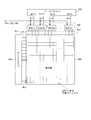
- FIG. 1 is a block diagram showing the overall configuration of an active matrix liquid crystal display device according to a first embodiment of the present invention.
- This liquid crystal display device includes a power source 100, a DC / DC converter 110, a display control circuit 200, a source driver (video signal line driving circuit) 300, a selection circuit (selection circuit) 400, and a gate driver (scanning signal line driving circuit) 500.
- a display unit 600 and a common electrode driving circuit 900 are provided.
- a plurality of source lines (video signal lines) are grouped in units of a predetermined number of source lines, and each group is connected to the source driver 300 via the selection circuit 400.
- This is a liquid crystal display device adopting a so-called SSD (Source Shared Driving) method.
- SSD Source Shared Driving
- the selection circuit 400 is formed on the liquid crystal display panel 700 including the display portion 600 using amorphous silicon, polycrystalline silicon, microcrystalline silicon, an oxide semiconductor (for example, IGZO) or the like. That is, in the liquid crystal display device according to this embodiment, the selection circuit 400 and the display unit 600 are formed on the same substrate (an array substrate that is one of the two substrates constituting the liquid crystal display panel). This is a selection circuit monolithic liquid crystal display device. Thereby, the frame area of the liquid crystal display device can be reduced.
- the source driver 300 and / or the gate driver 500 may also be formed over the liquid crystal display panel 700 using amorphous silicon, polycrystalline silicon, microcrystalline silicon, an oxide semiconductor, or the like. Specific implementation examples using these amorphous silicon and IGZO will be described later.
- the display unit 600 includes n source lines (video signal lines) SL1 to SLn, m gate lines (scanning signal lines) GL1 to GLm, source lines SL1 to SLn, and gate lines GL1 to GLm.
- M ⁇ n pixel forming portions provided corresponding to the respective intersections are formed.
- the m ⁇ n pixel forming portions are arranged in a matrix to constitute a pixel array.
- Each pixel forming portion includes a pixel thin film transistor 80 which is a switching element having a gate terminal connected to a gate line passing through a corresponding intersection and a source terminal connected to a source line passing through the intersection, and the pixel thin film transistor 80
- a pixel electrode connected to the drain terminal, a common electrode Ec which is a counter electrode provided in common to the plurality of pixel formation portions, and a pixel electrode provided in common to the plurality of pixel formation portions.
- the liquid crystal layer is sandwiched between the electrode Ec.
- a pixel capacitor Cp is constituted by a liquid crystal capacitor formed by the pixel electrode and the common electrode Ec.
- an auxiliary capacitor is provided in parallel with the liquid crystal capacitor in order to reliably hold the voltage in the pixel capacitor Cp.
- the auxiliary capacitor is not directly related to the present invention, its description and illustration are omitted.
- the pixel forming portion is configured as a set of three pixel forming portions corresponding to R, G, and B, respectively.
- One pixel is formed by this one set.
- the pixel formation portions corresponding to R, G, and B are referred to as “R pixel formation portion”, “G pixel formation portion”, and “B pixel formation portion”, respectively.
- the power supply 100 supplies a predetermined power supply voltage to the DC / DC converter 110, the display control circuit 200, and the common electrode drive circuit 900.
- the DC / DC converter 110 generates a predetermined DC voltage for operating the source driver 300 and the gate driver 500 from the power supply voltage and supplies it to the source driver 300 and the gate driver 500.
- the common electrode drive circuit 900 gives a predetermined potential Vcom to the common electrode Ec.
- the display control circuit 200 receives an image signal DAT and a timing signal group TG such as a horizontal synchronization signal and a vertical synchronization signal sent from the outside, and controls the digital video signal DV (image data) and image display on the display unit 600.
- the high level side potential of the selection control signal CT is Vdd potential, and the low level side potential is Vss potential.
- the selection control signal CT includes three-phase selection control signals CTr, CTg, and CTb. These selection control signals CTr, CTg, and CTb correspond to the R pixel forming portion, the G pixel forming portion, and the B pixel forming portion, respectively.
- the selection control signal CTr is referred to as an “R selection control signal”
- the selection control signal CTg is referred to as a “G selection control signal”
- the selection control signal CTb is referred to as a “B selection control signal”.
- the time when the high level potential changes to the low level potential from the time when each of the R selection control signal CTr, the G selection control signal CTg, and the B selection control signal CTb changes from the low level potential to the high level potential.
- the period up to is referred to as a “switching selection period” for convenience.
- the R selection control signal CTr, the G selection control signal CTg, and the B selection control signal CTb are out of phase with each other by one switching selection period, and each of them is only one switching selection period among the three switching selection periods. It becomes a high level potential (Vdd potential) (except for a rest period T2 described later).
- the three switching selection period corresponds to one horizontal scanning period.
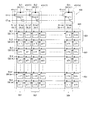
- the source driver 300 receives the digital video signal DV, the source start pulse signal SSP, the source clock signal SCK, and the latch strobe signal LS output from the display control circuit 200, and outputs video signals to the k output signal lines OL1 to OLk, respectively.
- SS (1) to SS (k) are given.
- k n / 3. A detailed description of this source driver will be described later.
- the selection circuit 400 includes an R selection control signal CTr, a G selection control signal CTg, and a B selection control signal CTb output from the display control circuit 200 and video signals SS (1) to SS output from the source driver 300. (K) is received, and these video signals SS (1) to SS (k) are time-divisionally applied to the source lines SL1 to SLn. A detailed description of the selection circuit 400 will be described later.
- the gate driver 500 supplies the high-level potential scanning signals GS (1) to GS (m) to the gate lines GL1 to GLm, respectively. Is repeated with one frame period as a cycle.
- the video signals SS (1) to SS (k) are applied in time division to the source lines SL1 to SLn, and the scanning signals GS (1) to GS (m) are applied to the gate lines GL1 to GLm, respectively.
- an image based on the image signal DAT sent from the outside is displayed on the display unit 600.
- FIG. 2 is a block diagram showing the configuration of the source driver 300 in this embodiment.
- the source driver 300 is connected to the shift register 310 having the number of stages equal to the number of the output signal lines OL1 to OLk, the sampling latch circuit 320 connected to the shift register 310, and the sampling latch circuit 320.
- an output circuit 330 connected to the output signal lines OL1 to OLk.
- the shift register 310 receives the source start pulse signal SSP and the source clock signal SCK output from the display control circuit 200. Based on the source start pulse signal SSP and the source clock signal SCK, the shift register 310 transmits a pulse included in the source start pulse signal SSP from the input end to the output end in each of the three switching selection periods in each horizontal scanning period. And sequentially transfer. In response to this transfer, sampling pulses are sequentially given to the sampling latch circuit 320.
- the sampling latch circuit 320 receives the digital video signal DV and the latch strobe signal LS output from the display control circuit 200 and the sampling pulse output from the shift register 310.
- the sampling latch circuit 320 holds the digital video signal DV at the timing of the sampling pulse, further latches it with the latch strobe signal LS, and holds it for each switching selection period (1/3 horizontal scanning period).
- the digital video signal DV held here is, for example, 8-bit data corresponding to each color.
- the held digital video signal DV is supplied to the output circuit 330.
- the output circuit 330 converts the digital video signal DV received from the sampling latch circuit 320 into an analog signal representing, for example, 256 gradations, and outputs the analog video signals to the output signal lines OL1 to OLk as video signals SS (1) to SS (k), respectively. Is done.
- these video signals SS (1) to SS (k) are R pixel forming portions in the first switching selection period (hereinafter referred to as “first switching selection period”) in each horizontal scanning period.
- first switching selection period hereinafter referred to as “second switching selection period”
- the potential corresponding to the G pixel formation portion and the third switching in each horizontal scanning period.
- the selection period hereinafter referred to as “third switching selection period”
- the potential corresponds to the B pixel formation portion.
- a level shift operation for shifting the potential of the video signal may be performed.
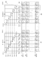
- FIG. 3 is a block diagram for explaining the configuration of the selection circuit 400 in the present embodiment.
- the selection circuit 400 includes k selection blocks 410 (1) to 410 (k).
- the display unit 600 is formed with an m-row ⁇ n-column pixel matrix as described above, and the selection block is provided so as to correspond to each column of these pixel matrices on a three-to-one basis.
- FIG. 4 is a circuit diagram for explaining the correspondence between the selection blocks 410 (1) to 410 (k) and the source lines SL1 to SLn in the present embodiment.
- the source lines SL1 to SLn are grouped into source line groups SG1 to SGk in units of three.
- the source line set SGj includes three source lines SL3j-2 to SL3j. These source line sets SG1 to SGk correspond to the selection blocks 410 (1) to 410 (k), respectively.
- a source line corresponding to R (hereinafter referred to as “R source line”) in the source line set SGj is represented by reference symbol SLrj, and a source line corresponding to G (hereinafter referred to as “G source line”).
- a source line corresponding to B (hereinafter referred to as a “B source line”) is represented by a symbol SLbj.
- the G pixel formation portion provided corresponding to is represented by reference symbol gij
- the B pixel formation portion provided corresponding to the intersection of the B source line SLbj and the gate line GLi is represented by reference symbol bij.
- Each selection block is composed of three thin film transistors as shown in FIG.
- the three thin film transistors in the selection block 410 (j) are referred to as an R thin film transistor 40r (j), a G thin film transistor 40g (j), and a B thin film transistor 40b (j), respectively.
- an R selection control signal CTr is applied to the gate terminal, an output signal line corresponding to the selected block including the R thin film transistor is connected to the source terminal, and the R signal is connected to the drain terminal.
- An R source line in a source line set corresponding to a selected block including a thin film transistor is connected.
- a G selection control signal CTg is given to the gate terminal, an output signal line corresponding to the selected block including the G thin film transistor is connected to the source terminal, and the G signal is connected to the drain terminal.
- the G source line in the source line set corresponding to the selected block including the thin film transistor is connected.
- the gate terminal is supplied with a B selection control signal CTb, the source terminal is connected to an output signal line corresponding to the selected block including the B thin film transistor, and the drain terminal is connected to the B thin film transistor.
- a source line for B in a source line set corresponding to a selected block including a thin film transistor is connected.
- the source terminal and the drain terminal of the thin film transistor are switched depending on the polarity of the video signal applied to the source terminal of each thin film transistor in the selected block.
- the terminal on the side to which the output signal line corresponding to the selected block is connected is used as the source terminal, and the source line corresponding to the selected block is used.
- the terminal on the side to which the source line in the set is connected will be described as the drain terminal.
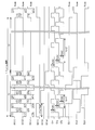
- FIG. 5 is a signal waveform diagram for explaining the detailed operation of the SSD liquid crystal display device according to this embodiment.
- one frame period is composed of a scanning period T1 and a pause period T2 provided after the scanning period T1.
- the scanning signals GS (1) to GS (m) are sequentially set to the high level potential based on the gate clock signal GCK.
- the suspension period T2 all of the m gate lines GL1 to GLm (scanning signals GS (1) to GS (m)) are at the low level potential.
- the respective frequencies (hereinafter referred to as “scanning period frequencies”) of the R selection control signal CTr, the G selection control signal CTg, and the B selection control signal CTb in the scanning period T1 are denoted by reference numeral fck1.
- the respective amplitudes (hereinafter referred to as “scanning period amplitude”) of the R selection control signal CTr, the G selection control signal CTg, and the B selection control signal CTb in the scanning period T1 are denoted by reference numeral Vck1.
- the video signal SS (j) has a potential corresponding to the R pixel forming portion rij in each of the first switching selection period to the third switching selection period in the i-th horizontal scanning period in the scanning period T1.
- the polarity of each video signal is inverted every switching selection period, the polarity of the video signal applied to the output signal lines adjacent to each other is inverted, and each frame period
- the polarity inversion drive is performed by inverting the polarity of each video signal, the present invention is not limited to this.
- the gate line GL1 is selected when the scanning signal GS (1) becomes a high level potential, the R pixel forming unit r1j, the G subpixel forming unit g1j, and the B pixel forming unit b1j can write video signals. It becomes a state.
- a period in which the gate line GL1 is in a selected state is referred to as a “first selection period”.
- the R selection control signal CTr is at a high level potential in the first switching selection period
- the R thin film transistor 40r (j) shown in FIG. 4 is turned on. Therefore, the video signal SS (j) having a potential corresponding to the R pixel formation portion r1j is given to the R source line SLrj.
- the potential of the R source line SLrj (the video signal SS (j) having a potential corresponding to the R pixel formation portion r1j) is written into the R pixel formation portion r1j. Note that in this first selection period, the odd-numbered R source lines SLrj change to positive polarity, and the even-numbered R source lines SLrj change to negative polarity.
- the G source line SLgj and the B source line SLbj maintain the potential (Vcom potential) in the preceding pause period T2.
- the G selection control signal CTg is at a high level potential
- the G thin film transistor 40g (j) shown in FIG. 4 is turned on. Therefore, the video signal SS (j) having a potential corresponding to the G pixel forming portion g1j is given to the G source line SLgj.
- the potential of the G source line SLgj (the video signal SS (j) having a potential corresponding to the G pixel formation portion g1j) is written into the G pixel formation portion g1j. Note that in this first selection period, the odd-numbered G source lines GLgj change to negative polarity, and the even-numbered G source lines SLgj change to positive polarity.
- the R source line SLrj and the B source line SLbj maintain the potential in the first switching selection period.
- the B selection control signal SPCkb is at a high level potential
- the B thin film transistor 40b (j) shown in FIG. 4 is turned on. Therefore, the video signal SS (j) having a potential corresponding to the B pixel formation portion b1j is supplied to the B source line SLbj.
- the potential of the B source line SLbj (the video signal SS (j) having a potential corresponding to the B pixel formation portion b1j) is written to the B pixel formation portion b1j. Note that in this first selection period, the odd-numbered B source lines GLbj change to positive polarity, and the even-numbered B source lines SLbj change to negative polarity.
- the R source line SLrj and the G source line SLgj maintain the potential in the second switching selection period.
- the pause period T2 is longer than the scanning period T1.
- the present invention is not limited to this, and the pause period T2 may be shorter than the scanning period T1.
- the R selection control signal CTr, the G selection control signal CTg, and the B selection control signal CTb have a period longer than the scanning period period tck1, and the first switching selection period.
- the second switching selection period and the third switching selection period each becomes a high level potential.
- the periods (hereinafter referred to as “pause period periods”) of the R selection control signal CTr, the G selection control signal CTg, and the B selection control signal CTb in the suspension period T2 are denoted by reference numeral tck2.
- pause period frequencies the respective frequencies (hereinafter referred to as “pause period frequencies”) of the R selection control signal CTr, the G selection control signal CTg, and the B selection control signal CTb in the pause period T2 are denoted by reference symbol fck2.
- pause period amplitude the respective amplitudes (hereinafter referred to as “pause period amplitude”) of the R selection control signal CTr, the G selection control signal CTg, and the B selection control signal CTb in the pause period T2 are denoted by reference sign Vck2.
- the idle period cycle tck2 is longer than the scanning period cycle tck1. That is, the idle period frequency fck2 is lower than the scanning period frequency fck1.
- the scanning period frequency fck1 is an integral multiple of the idle period frequency fck2.
- the display control circuit 200 and the like can have a simple configuration.
- the scanning period frequency fck1 is at least twice the idle period frequency fck2.
- the idle period frequency fck2 is 1 ⁇ 2 times or less of the scanning period frequency fck1.
- the power consumption required for driving the selection circuit 400 can be sufficiently reduced.
- Such control of the frequency (cycle) of the selection control signal CT is performed in the display control circuit 200, for example.
- the idle period amplitude Vck2 and the scanning period amplitude Vck1 are the same.
- the video signal SS (j) is at the Vcom potential during the idle period T2. Further, since the scanning signals GS (1) to GS (m) do not become a high level potential during the pause period T2, the video signal is written to the R pixel forming portion rij, the G pixel forming portion gij, and the B pixel forming portion bij. Absent.
- the R selection control signal CTr becomes a high level potential in the first switching selection period in the first period in the pause period T2 having the same length as the one horizontal scanning period (hereinafter simply referred to as “one horizontal scanning period”)
- the R thin film transistor 40r (j) shown in FIG. 4 is turned on. Therefore, the video signal SS (j) having the Vcom potential is supplied to the R source line SLrj.
- the G source line SLgj and the B source line SLbj maintain the potential in the preceding scanning period T1.
- the G selection control signal CTg becomes a high level potential
- the G thin film transistor 40g (j) shown in FIG. 4 is turned on. Therefore, the video signal SS (j) having the Vcom potential is supplied to the G source line SLgj.
- the R source line SLrj maintains the Vcom potential
- the B source line SLbj maintains the potential in the preceding scanning period T1.
- the B selection control signal CTb becomes a high level potential
- the B thin film transistor 40b (j) shown in FIG. 4 is turned on. Therefore, the video signal SS (j) having the Vcom potential is supplied to the B source line SLbj.
- the R source line SLrj and the G source line SLgj maintain the Vcom potential.
- the selection circuit 400 is used in the suspension period T2 in order to fix the source line to a predetermined potential (Vcom potential) in the suspension period T2. It is conceivable to keep each thin film transistor in the OFF state or keep the thin film transistor in the ON state during the rest period T2 and set each video signal to the Vcom potential.
- the source line is in a floating state. For this reason, the source line is likely to be affected by noise or the like in the pause period T2. Since there is a parasitic capacitance between the source line and the pixel electrode, and the pixel electrode is also in a floating state, noise in the source line also affects the pixel potential due to capacitive coupling. As a result, the display quality may be degraded.
- the potentials of the R selection control signal CTr, the G selection control signal CTg, and the B selection control signal CTb are high for each pause period tck2.
- each of the R thin film transistor, the G thin film transistor, and the B thin film transistor is turned on. For this reason, the Vcom potential is applied to each source line at each pause period tck2. Thereby, in this embodiment, the influence of the noise etc. which a source line receives in the idle period T2 is reduced. As a result, it is possible to suppress deterioration in display quality.
- each thin film transistor in the selection circuit 400 is kept in the on state and the video signal is set to the Vcom potential in the pause period T2, it is necessary to continuously apply a high level potential to the gate terminal of the thin film transistor. Since the gate bias stress is applied to the thin film transistor for a long time, the threshold fluctuation in the thin film transistor is increased. As a result, the thin film transistor is lowered. On the other hand, in the present embodiment, the high-level potential is only given to the gate terminal of each thin film transistor in the selection circuit 400 for each pause period tck2. Thereby, in this embodiment, since the gate bias stress applied to the thin film transistor is reduced, the threshold fluctuation in the thin film transistor is reduced. As a result, it is possible to suppress a decrease in dynamic performance (reliability) of the thin film transistor M2.
- a-Si or an oxide semiconductor can be used for the semiconductor layer of each thin film transistor in the selection circuit 400 in this embodiment.
- the oxide semiconductor typically, InGaZnO x (hereinafter referred to as “IGZO”), which is an oxide semiconductor mainly containing indium, gallium, zinc, and oxygen, is used. It is not limited. For example, any oxide semiconductor containing at least one of indium, gallium, zinc, copper, silicon, tin, aluminum, calcium, germanium, and lead may be used.
- FIG. 6 is a graph showing drain current-gate voltage characteristics of a TFT using a-Si TFT and IGZO as a semiconductor layer (hereinafter referred to as “IGZOTFT”).
- the horizontal axis represents the gate voltage Vg
- the vertical axis represents the drain current Ids.
- the leakage current of the IGZOTFT is 1/1000 or less of the leakage current of the a-Si TFT
- the on-current of the IGZOTFT is about 20 times the on-current of the a-Si TFT.
- the driving power of the selection circuit 400 is reduced even when the a-Si TFT is used as this thin film transistor. It can be reduced (1/100 or less).
- the IGZOTFT has a large on-state current as described above, when the IGZOTFT is used, the size of the TFT can be reduced to about 1/20 compared to the case where the a-Si TFT is used.
- this embodiment can be realized at a lower cost than when an IGZO TFT is used.
- the idle period T2 is provided after the scanning period T1 within one frame period.
- the potentials of the R selection control signal CTr, the B selection control signal CTb, and the G selection control signal CTg become high for each pause period tck2 in the pause period T2.
- the R thin film transistor, the B thin film transistor, and the G thin film transistor are each turned on every idle period cycle tck2. This reduces the influence of noise and the like that the source line receives during the pause period T2, and threshold fluctuations in the R thin film transistor, the B thin film transistor, and the G thin film transistor. Accordingly, it is possible to suppress deterioration in display quality and to improve the reliability of the R thin film transistor, the B thin film transistor, and the G thin film transistor.
- the pause period T2 is provided longer than the scanning period T1, further power consumption can be achieved.
- the leakage current of the IGZOTFT is sufficiently small, so that the idle period frequency fck2 can be further reduced. For this reason, power consumption can be reduced.
- the TFT size can be sufficiently reduced. Thereby, further narrowing of the frame can be achieved.
- FIG. 7 is a circuit diagram for explaining the configuration of the selection circuit 400 and the correspondence between the selection blocks 410 (1) to 410 (k) and the source lines SL1 to SLn in the modification of the present embodiment.
- the selection control signal CT includes six-phase selection control signals CTr1, CTg1, CTb1, CTr2, CTg2, and CTb2.
- the selection control signals CTr1 and CTr2 correspond to the R pixel formation unit
- the selection control signals CTg1 and CTg2 correspond to the G pixel formation unit
- the selection control signals CTb1 and CTb2 correspond to the B pixel formation unit.
- the source line groups SG1 to SGk are grouped in units of six.
- Each source line group has two source lines corresponding to the same color.
- first R source line one of the two R source lines (hereinafter referred to as “first R source line”) and the other (hereinafter referred to as “second R source line”) in the source line set SGj are denoted by reference characters SLrj_1.
- second G source line one of the two G source lines (hereinafter referred to as “first G source line”) and the other (hereinafter referred to as “second G source line”) are denoted by reference numerals SLgj_1 and SLgj_2, respectively.
- first B source line first B source line
- second B source line second B source line
- the R pixel forming portion provided corresponding to the intersection of the first G is represented by rij_2
- the G pixel forming portion provided corresponding to the intersection of the first G source line SLgj_1 and the gate line GLi is represented by gij_1
- a G pixel forming portion provided corresponding to the intersection of the 2G source line SLgj_2 and the gate line GLi is denoted by reference symbol gij_2
- the pixel formation portion is denoted by reference numeral bij_1, and the second B source line SLbj_2 and the gate line GLi are connected to each other.
- the B pixel formation portions provided in correspondence to the difference point is indicated by reference numeral Bij_2.
- the six source lines in each source line set in this modification correspond to the three primary colors (that is, 2 ⁇ 3 primary colors) for two pixels, respectively.
- the selection block 410 (j) includes six thin film transistors 40r1 (j), 40g1 (j), 40b1 (j), 40r2 (j), 40g2 (j), and 40b2 (j).
- the six thin film transistors 40r1 (j), 40g1 (j), 40b1 (j), 40r2 (j), 40g2 (j), and 40b2 (j) are respectively the first R source line and the first G in the source line set SGj. This corresponds to the source line for 1B, the source line for 1B, the source line for 2R, the source line for 2G, and the source line for 2B.
- FIG. 8 is a signal waveform diagram for explaining the detailed operation of the SSD type liquid crystal display device according to this modification.
- a video signal is given to each video signal line by repeating one horizontal scanning period consisting of six switching selection periods in the scanning period T1.
- the basic operation in the scanning period T1 is the same as that in the first embodiment, and a description thereof will be omitted.
- the basic operation in the suspension period T2 is also the same as that in the first embodiment, and a description thereof will be omitted.
- the number of output terminals (the number of output signal lines) of the source driver 300 is reduced as compared with the first embodiment, so that further cost reduction can be achieved.
- FIG. 9 is a signal waveform diagram for explaining the detailed operation of the liquid crystal display device according to the second embodiment of the present invention. Since the present embodiment is the same as the first embodiment except for the operation during the suspension period, the description of the same portion is omitted.
- the pause period amplitude Vck2 is smaller than the scanning period amplitude Vck1.
- the idle period amplitude Vck2 needs to be larger than the threshold voltage of the thin film transistor. That is, the pause period amplitude Vck2 in the present embodiment is smaller than the scanning period amplitude Vck1 and larger than the threshold voltage of each thin film transistor in the selection circuit 400.
- the idle period amplitude Vck2 that is the amplitude of each of the R selection control signal CTr, the G selection control signal CTg, and the B selection control signal CTb in the pause period T2 is R-use in the scan period T1. It is smaller than the scanning period amplitude Vck1, which is the amplitude of each of the selection control signal CTr, the G selection control signal CTg, and the B selection control signal CTb. For this reason, further reduction in power consumption can be achieved.
- the gate bias stress applied to the R thin film transistor, the G thin film transistor, and the B thin film transistor is further reduced during the suspension period T2, the R thin film transistor, the G thin film transistor, and the B thin film transistor are further improved in reliability. Can be achieved.
- FIG. 10 is a circuit diagram for explaining the configuration of the selection circuit 400 and the correspondence between the selection blocks 410 (1) to 410 (k) and the source lines SL1 to SLn in the third embodiment of the present invention. .
- this embodiment is the same as the first embodiment except for the configuration of the selection circuit 400 and the detailed operation of the liquid crystal display device, and thus the description of the same parts is omitted.
- a color image display using the four primary colors RGBY is performed.
- the pixel forming portion is configured as a set of four pixel forming portions corresponding to R, G, B, and Y, respectively. One pixel is formed by this one set.
- the pixel forming portion corresponding to Y is referred to as “Y pixel forming portion”.
- One pixel composed of RGBY includes an R pixel formation portion and a B pixel formation portion provided corresponding to the preceding gate line in each gate line set, and a Y provided corresponding to the gate line subsequent to the gate line. This is realized by the pixel forming unit and the G pixel forming unit.
- the selection control signal CT is composed of two-phase selection control signals CTry and CTbg.
- the selection control signal CTry corresponds to the R pixel formation portion and the Y pixel formation portion
- the selection control signal CTbg corresponds to the B pixel formation portion and the G pixel formation portion.
- the selection control signal CTry is referred to as “RY selection control signal”
- the selection control signal CTbg is referred to as “BG selection control signal”.
- switch selection is performed for the period from the time when each of the RY selection control signal CTry and the BG selection control signal CTbg changes from the low level potential to the high level potential until the time when the RY selection control signal CTbg changes from the high level potential to the low level potential.
- the RY selection control signal CTry and the BG selection control signal CTbg are out of phase with each other by one switching selection period, and both are at a high level potential (Vdd potential) only during one switching selection period in the two switching selection period. (However, excluding the suspension period T2).
- the two switching selection period corresponds to one horizontal scanning period.
- the selection circuit 400 in the present embodiment is configured by k selection blocks 410 (1) to 410 (k) as in the first embodiment.
- Output signal lines OL1 to OLk are connected to (corresponding to) the selection blocks 410 (1) to 410 (k), respectively.
- two different source lines are connected to each of the selection blocks 410 (1) to 410 (k).
- Each selection block is provided with an RY selection control signal CTry and a BG selection control signal CTbg.
- the source lines SL1 to SLn are grouped into source line groups SG1 to SGk in units of two.
- the source line set SGj is composed of two source lines SL2j-1 and SL2j. These source line sets SG1 to SGk correspond to the selection blocks 410 (1) to 410 (k), respectively.
- a source line corresponding to R and Y (hereinafter referred to as “RY source line”) in the source line set SGj is represented by reference symbol SLryj, and a source line corresponding to B and G (hereinafter referred to as “BG source line”). ”) Is represented by the symbol SLbgj.
- the R pixel forming portion provided corresponding to the intersection of the RY source line SLryj and the gate line GL2i-1 is represented by reference numeral rij and corresponds to the intersection of the BG source line SLbgj and the gate line GL2i-1.
- a G pixel forming portion provided corresponding to an intersection with the line GL2i is represented by reference symbol gij.
- Each selection block is composed of two thin film transistors as shown in FIG.
- the two thin film transistors in the selection block 410 (j) are referred to as an RY thin film transistor 40ry (j) and a BG thin film transistor 40bg (j), respectively.
- the gate terminal is supplied with the RY selection control signal CTry, the source terminal is connected to the output signal line corresponding to the selected block including the RY thin film transistor, and the drain terminal is connected to the RY thin film transistor.
- RY source lines in a source line set corresponding to a selected block including a thin film transistor are connected.
- a BG selection control signal CTbg is given to the gate terminal, an output signal line corresponding to the selected block including the BG thin film transistor is connected to the source terminal, and the BG use is connected to the drain terminal.
- a BG source line in a source line set corresponding to a selected block including a thin film transistor is connected.
- Such a selection circuit 400 realizes an operation of applying the video signals SS (1) to SS (k) to the source lines SL1 to SLn in a time division manner.
- FIG. 11 is a signal waveform diagram for explaining the detailed operation of the SSD liquid crystal display device according to this embodiment.
- these video signals SS (1) to SS (k) become potentials corresponding to the Y pixel forming portion in the first switching selection period in the subsequent one horizontal scanning period among the two consecutive horizontal scanning periods, and In the second switching selection period in the subsequent one horizontal scanning period, the potential corresponds to the G pixel formation portion.
- the RY selection control signal CTry and the BG selection control signal CTbg are at high level potentials in the first switching selection period and the second switching selection period, respectively. That is, each cycle of the RY selection control signal CTry and the BG selection control signal CTbg is one horizontal scanning period (two switching selection periods).
- the R selection control signal CTr in the scanning period T1 in the first embodiment is also used for the respective periods of the RY selection control signal CTry and the BG selection control signal CTbg in the scanning period T1 in the present embodiment.
- the respective periods of the G selection control signal CTg and the B selection control signal CTb they are referred to as “scanning period period tck1”.
- the R selection control signal CTr in the scanning period T1 in the first embodiment Similarly to the frequencies of the G selection control signal CTg and the B selection control signal CTb, they are referred to as “scan period frequency fck1”.
- the gate line GL1 is selected (becomes the first selection period), so that the R pixel formation portion r1j and the B pixel formation portion b1j can write a video signal. It becomes a state.
- the RY selection control signal CTry is at a high level potential in the first switching selection period
- the RY thin film transistor 40ry (j) shown in FIG. 10 is turned on. Therefore, the video signal SS (j) having a potential corresponding to the R pixel formation portion r1j is given to the RY source line SLryj.
- the potential of the RY source line SLryj (the video signal SS (j) having a potential corresponding to the R pixel formation portion r1j) is written into the R pixel formation portion r1j.
- the odd-numbered RY source lines SLryj change to positive polarity
- the even-numbered RY source lines SLryj change to negative polarity.
- the BG source line SLbgj maintains the potential (Vcom potential) in the preceding pause period T2.
- the BG selection control signal CTbg becomes a high level potential
- the BG thin film transistor 40bg (j) shown in FIG. 10 is turned on. Therefore, the video signal SS (j) having a potential corresponding to the B pixel formation portion b1j is supplied to the BG source line SLbgj.
- the potential of the BG source line SLbgj (the video signal SS (j) having a potential corresponding to the B pixel formation portion b1j) is written into the B pixel formation portion b1j.
- the odd-numbered BG source line SLbgj changes to negative polarity
- the even-numbered BG source line SLbgj changes to positive polarity.
- the RG source line SLryj maintains the potential in the first switching selection period.
- the gate line GL2 is in a selected state, so that the Y pixel forming portion y1j and the G pixel forming portion g1j are in a state in which a video signal can be written.
- a period during which the gate line GL2 is in a selected state is referred to as a “second selection period”.
- the RY thin film transistor 40ry (j) is turned on as in the first switching selection period of the first selection period, but the RY source line SLryj has a potential corresponding to the Y pixel formation portion y1j.
- a video signal SS (j) is given.
- the potential of the RY source line SLryj (the video signal SS (j) having a potential corresponding to the Y pixel formation portion y1j) is written to the Y pixel formation portion y1j.
- the RY source line SLryj has the same polarity as that in the first selection period.
- the BG source line SLbgj maintains the potential in the second switching selection period of the first selection period.
- the BG thin film transistor 40bg (j) is turned on as in the second switching selection period of the first selection period, but the BG source line SLbgj has a G pixel forming portion.
- a video signal SS (j) having a potential corresponding to g1j is supplied.
- the potential of the BG source line SLbgj (the video signal SS (j) having a potential corresponding to the G pixel formation portion g1j) is written into the G pixel formation portion g1j.
- the BG source line SLbgj has the same polarity as that in the first selection period.
- the RY source line SLrj maintains the potential in the first switching selection period of the second selection period.
- the operation of the liquid crystal display device in the suspension period T2 will be described with reference to FIGS.
- the RY selection control signal CTry and the BG selection control signal CTbg are longer than the scanning period period tck1, and are respectively in the first switching selection period and the second switching selection period. High level potential.
- the R selection control signal CTr during the pause period T2 in the first embodiment is also used for each cycle of the RY selection control signal CTry and the BG selection control signal CTbg during the pause period T2 in the present embodiment.
- the periods of the G selection control signal CTg and the B selection control signal CTb are referred to as “pause period period tck2.”
- the R selection control signal CTr in the suspension period T2 in the first embodiment Similarly to the frequencies of the G selection control signal CTg and the B selection control signal CTb, they are referred to as “pause period frequency fck2.”
- the pause period cycle tck2 is longer than the scanning period cycle tck1. That is, the idle period frequency fck2 is lower than the scanning period frequency fck1. Note that the relationship between the scanning period frequency fck1 and the idle period frequency fck2 is the same as that in the first embodiment, and a description thereof will be omitted.
- the video signal SS (j) is at the Vcom potential. Further, since the scanning signals GS (1) to GS (m) do not become a high level potential during the rest period T2, the R pixel formation unit rij, the G pixel formation unit gij, the B pixel formation unit bij, and the Y pixel formation unit yij No video signal is written.
- the RY selection control signal CTry becomes a high level potential in the first switching selection period
- the RY thin film transistor 40ry (j) shown in FIG. 10 is turned on. Therefore, the video signal SS (j) having the Vcom potential is supplied to the RY source line SLryj.
- the BG source line SLbgj maintains the potential in the preceding scanning period T1.
- the BG selection control signal CTbg becomes a high level potential
- the BG thin film transistor 40bg (j) shown in FIG. 10 is turned on. Therefore, the video signal SS (j) having the Vcom potential is supplied to the BG source line SLbgj. Note that the RY source line SLryj maintains the Vcom potential in the second switching selection period.
- the same effect as in the first embodiment can be achieved in a liquid crystal display device in which pixels of RGBY are formed across two gate lines.
- FIG. 12 is a circuit diagram for explaining the configuration of the selection circuit 400 according to the fifth embodiment of the present invention. Since this embodiment is the same as the first embodiment except for the configuration of the selection circuit 400, the description of the same portion is omitted. As shown in FIG. 12, the selection circuit 400 in this embodiment is configured separately on both sides (upper and lower sides in FIG. 12) of the display unit 600. Hereinafter, the side on which the source driver 300 is arranged with respect to the display unit 600 is referred to as “upper side”, and the opposite side of the upper side with respect to the display unit 600 is referred to as “lower side”.
- the upper part of the display unit 600 corresponds to the first selection circuit
- the lower part of the display unit 600 corresponds to a second selection circuit.
- the first selection circuit and the second selection circuit share each selection block. More specifically, each selection block in the selection circuit 400 is configured separately on the upper side and the lower side of the display unit 600.
- the odd-numbered selection block counted from the side where the gate driver 500 is arranged is composed of an R thin film transistor and a B thin film transistor arranged on the upper side, and a G thin film transistor arranged on the lower side.
- the even-numbered selection block counted from the side where the gate driver 500 is arranged is composed of the G thin film transistor arranged on the upper side, and the R thin film transistor and the B thin film transistor arranged on the lower side.
- a video signal is given to the source terminals of the R thin film transistor, the G thin film transistor, and the B thin film transistor arranged on the lower side by wiring extending from the upper side to the lower side of the display portion 600. Note that the connection of each thin film transistor and the signal given to each thin film transistor are the same as in the first embodiment, and a description thereof will be omitted.
- the number of thin film transistors (respective sizes of the first selection circuit and the second selection circuit) in the selection circuit 400 necessary for the upper side and the lower side of the display unit 600 is the same as that of the first embodiment.
- the number of thin film transistors in the selection circuit 400 in the embodiment is about half. For this reason, the layout pitch in the extending direction of the gate line is doubled. Thereby, for example, it becomes possible to deal with a higher-definition liquid crystal display panel.
- color image display is performed using a combination of the four primary colors RGBY, but the present invention is not limited to this.
- the present invention can also be applied to color image display using a combination of other four primary colors such as RGBW.
- each source line set may be constituted by source lines such as 9, 12, 15,...
- each selected block is configured by the same number of thin film transistors as the number of source lines constituting the source line set.
- the thin film transistors are all assumed to be n-channel type, but the present invention is not limited to this. The present invention can be applied even if the thin film transistor is a p-channel type.
- the liquid crystal display device has been described as an example, but the present invention is not limited to this.
- the present invention can also be applied to other display devices such as organic EL (Electro Luminescence) display devices.
- organic EL Electro Luminescence
- the above-described embodiments can be variously modified and implemented without departing from the spirit of the present invention.
- an SSD display device with reduced power consumption and a method for controlling a selection circuit in the display device can be provided.
- the present invention can be applied to an SSD display device.
Abstract
Description
複数の映像信号線および該複数の映像信号線と交差する複数の走査信号線を含む表示部と、
前記複数の走査信号線が順次選択される走査期間と該複数の走査信号線のいずれもが非選択状態となる休止期間とが、該走査期間と該休止期間とからなるフレーム期間を周期として交互に現れるように、前記複数の走査信号線を駆動するための走査信号線駆動回路と、
前記表示部と一体的に形成され、複数の選択ブロックを含む選択回路と、
前記複数の選択ブロックにそれぞれ複数の映像信号を与える映像信号線駆動回路と、
前記映像信号線駆動回路に前記複数の映像信号に対応する画像データを与え、各選択ブロックにオンレベルとオフレベルとを周期的に繰り返す複数の選択制御信号を与える表示制御回路とを備え、
各選択ブロックが、前記複数の選択制御信号と同数の互いに隣接する映像信号線を単位とする映像信号線組における各映像信号線に、該選択ブロックが受け取る前記映像信号を該複数の選択制御信号に基づいて時分割して与え、
前記表示制御回路が、前記休止期間における前記複数の選択制御信号の周波数を前記走査期間における該複数の選択制御信号の周波数よりも低くする該複数の選択制御信号を生成することを特徴とする。
前記表示制御回路が、前記休止期間における前記複数の選択制御信号の振幅を前記走査期間における該複数の選択制御信号の振幅よりも小さくするように該複数の選択制御信号を生成することを特徴とする。
前記休止期間が前記走査期間よりも長いことを特徴とする。
前記映像信号線駆動回路が、前記休止期間における前記映像信号の電位を固定電位にすることを特徴とする。
各選択ブロックは、該選択ブロックに対応する映像信号線組内の複数の映像信号線にそれぞれ第1導通端子が接続された複数のスイッチング素子を有し、
各選択ブロックにおける前記複数のスイッチング素子の第2導通端子には、該選択ブロックが受け取る前記映像信号が与えられ、
前記表示制御回路が、各選択ブロックにおける前記複数のスイッチング素子にそれぞれ前記複数の選択制御信号を与えることを特徴とする。
前記表示部が複数の原色に基づく画像を表示し、
各映像信号線組における複数の映像信号線が、前記複数の原色にそれぞれ対応することを特徴とする。
前記複数の原色が3原色であり、
各映像信号線組が3本の映像信号線からなり、
各選択ブロックが3つのスイッチング素子を有し、
各映像信号線組における前記3本の映像信号線が、前記3原色にそれぞれ対応することを特徴とする。
前記表示部が複数の原色に基づく画像を表示し、
各映像信号線組における複数の映像信号線が、該映像信号線数よりも多い所定数の原色のうちの、該映像信号線と同数の原色にそれぞれ対応すると共に、該所定数の原色のうちの、該映像信号線と同数の他の原色にそれぞれ対応することを特徴とする。
前記複数の原色が4原色であり、
各映像信号線組が2本の映像信号線からなり、
各選択ブロックが2つのスイッチング素子を有し、
各映像信号線組における前記2本の映像信号線が、前記4原色のうちの2色にそれぞれ対応すると共に、該4原色のうちの他の2色にそれぞれ対応することを特徴とする。
前記表示部が複数の原色に基づく画像を表示し、
各映像信号線組が、前記複数の原色の数の整数倍の映像信号線からなることを特徴とする。
前記複数の原色が3原色であり、
各映像信号線組が6本の映像信号線からなり、
各選択ブロックが6つのスイッチング素子を有し、
各映像信号線組における3本の映像信号線が前記3原色にそれぞれ対応し、該映像信号線組における他の3本の映像信号線が該3原色にそれぞれ対応することを特徴とする。
前記選択回路は、
前記表示部に対して一方に位置する第1選択回路と、
前記表示部に対して他方に位置する第2選択回路とにより構成されることを特徴とする。
前記選択回路が、酸化物半導体により半導体層が形成された薄膜トランジスタを用いて実現されていることを特徴とする。
前記選択回路が、アモルファスシリコンにより半導体層が形成された薄膜トランジスタを用いて実現されていることを特徴とする。
前記複数の走査信号線が順次選択される走査期間と該複数の走査信号線のいずれもが非選択状態となる休止期間とが、該走査期間と該休止期間とからなるフレーム期間を周期として交互に現れるように、前記複数の走査信号線を駆動するステップと、
前記複数の選択制御信号と同数の互いに隣接する映像信号線を単位とする映像信号線組における各映像信号線に、該選択ブロックが受け取る前記映像信号を前記複数の選択制御信号に基づいて時分割して与えるステップと、
前記休止期間における前記複数の選択制御信号の周波数を、前記走査期間における該複数の選択制御信号の周波数よりも低くするステップとを備えることを特徴とする。
前記休止期間における前記複数の選択制御信号の振幅が、前記走査期間における該複数の選択制御信号の振幅よりも小さいことを特徴とする。
前記休止期間が前記走査期間よりも長いことを特徴とする。
前記休止期間における前記映像信号の電位が固定電位であることを特徴とする。
<1.1 全体構成および動作>
図1は、本発明の第1の実施形態に係るアクティブマトリクス型の液晶表示装置の全体構成を示すブロック図である。この液晶表示装置は、電源100とDC/DCコンバータ110と表示制御回路200とソースドライバ(映像信号線駆動回路)300と選択回路(選択回路)400とゲートドライバ(走査信号線駆動回路)500と表示部600と共通電極駆動回路900とを備えている。本実施形態に係る液晶表示装置は、複数のソースライン(映像信号線)が所定数のソースラインを単位として組み分けされ、各組が選択回路400を介してソースドライバ300に接続されている、いわゆるSSD(Source Shared Driving:ソース・シェアド・ドライビング)方式を採用した液晶表示装置である。
図2は、本実施形態におけるソースドライバ300の構成を示すブロック図である。図2に示すように、このソースドライバ300は、出力信号線OL1~OLkの本数に等しい段数のシフトレジスタ310と、シフトレジスタ310に接続されたサンプリングラッチ回路320と、サンプリングラッチ回路320に接続され、出力信号線OL1~OLkに接続された出力回路330とにより構成されている。
図3は、本実施形態における選択回路400の構成を説明するためのブロック図である。図3に示すように、この選択回路400は、k個の選択ブロック410(1)~410(k)により構成されている。表示部600には上述のようにm行×n列の画素マトリクスが形成されており、これらの画素マトリクスの各列と3対1で対応するように上記選択ブロックが設けられている。
図5は、本実施形態に係るSSD方式の液晶表示装置の詳細な動作を説明するための信号波形図である。本実施形態では、図5に示すように、1フレーム期間が走査期間T1と、当該走査期間T1の後に設けられた休止期間T2とからなっている。この走査期間T1では走査信号GS(1)~GS(m)がゲートクロック信号GCKに基づいて順次にハイレベル電位になる。一方休止期間T2では、m本のゲートラインGL1~GLm(走査信号GS(1)~GS(m))のいずれもがローレベル電位になっている。
上記図4および図5を参照しつつ、走査期間T1における液晶表示装置の動作について説明する。図5に示すように、この走査期間T1では、R用選択制御信号CTr、G用選択制御信号CTg、およびB用選択制御信号CTbは、第1切替選択期間、第2切替選択期間、および第3切替選択期間でそれぞれハイレベル電位になる。すなわち、走査期間T1におけるR用選択制御信号CTr、G用選択制御信号CTg、およびB用選択制御信号CTbのそれぞれの周期(以下「走査期間周期」という)は1水平走査期間(3切替選択期間)である。なお、この走査期間周期を符号tck1で表す。また、走査期間T1におけるR用選択制御信号CTr、G用選択制御信号CTg、およびB用選択制御信号CTbのそれぞれの周波数(以下「走査期間周波数」という)を符号fck1で表す。また、走査期間T1におけるR用選択制御信号CTr、G用選択制御信号CTg、およびB用選択制御信号CTbのそれぞれの振幅(以下「走査期間振幅」という)を符号Vck1で表す。
次に、上記図4および図5を参照しつつ、休止期間T2における液晶表示装置の動作について説明する。本実施形態および後述の各実施形態では、休止期間T2が走査期間T1よりも長く設けられている。ただし、本発明はこれに限定されるものではなく、休止期間T2が走査期間T1よりも短くても良い。
上記選択回路モノリシック型の液晶表示装置において特許文献2に記載の駆動方法を単純に用いる場合、休止期間T2においてソースラインを所定電位(Vcom電位)に固定するために、休止期間T2において選択回路400内の各薄膜トランジスタをオフ状態に維持するか、または、休止期間T2において当該薄膜トランジスタをオン状態維持すると共に各映像信号をVcom電位にすることが考えられる。
本実施形態における選択回路400内の各薄膜トランジスタの半導体層には、例えば、a-Siまたは酸化物半導体等を用いることができる。なお、酸化物半導体としては、典型的には、インジウム、ガリウム、亜鉛、および酸素を主成分とする酸化物半導体であるInGaZnOx(以下、「IGZO」という)が用いられるが本発明はこれに限定されるものではない。例えば、インジウム、ガリウム、亜鉛、銅、珪素、錫、アルミニウム、カルシウム、ゲルマニウム、および鉛のうち少なくとも1つを含む酸化物半導体であれば良い。
本実施形態によれば、選択回路モノリシック型の液晶表示装置において、1フレーム期間内で走査期間T1の後に休止期間T2が設けられる。選択回路400内の薄膜トランジスタR用薄膜トランジスタ、B用薄膜トランジスタ、およびG用薄膜トランジスタにそれぞれ与えられるR用選択制御信号CTr、B用選択制御信号CTb、およびG用選択制御信号CTgの休止期間周波数fck2が、これらの走査期間周波数fck1よりも低いので、1フレーム期間全体での選択回路400の駆動周波数が低減される。このため、消費電力が低減される。また、選択回路400がモノリシック化されて形成されているので、液晶表示パネル700の額縁面積が縮小されると共に、選択回路400のコストが低減される。
図7は、本実施形態の変形例における選択回路400の構成、および選択ブロック410(1)~410(k)とソースラインSL1~SLnとの対応関係を説明するための回路図である。選択制御信号CTは6相の選択制御信号CTr1、CTg1、CTb1、CTr2、CTg2、およびCTb2からなっている。選択制御信号CTr1およびCTr2はR画素形成部に対応し、選択制御信号CTg1およびCTg2はG画素形成部に対応し、選択制御信号CTb1およびCTb2はB画素形成部に対応している。
<2.1 休止期間の動作>
図9は、本発明の第2の実施形態における液晶表示装置の詳細な動作を説明するための信号波形図である。なお、本実施形態は、休止期間の動作を除き上記第1の実施形態と同様であるので、当該同様の部分についての説明を省略する。本実施形態における休止期間振幅Vck2は走査期間振幅Vck1よりも小さい。なお、休止期間T2において選択回路400内の各薄膜トランジスタを確実にオン状態にするためには、この休止期間振幅Vck2はこの薄膜トランジスタのしきい値電圧よりも大きい必要がある。すなわち、本実施形態における休止期間振幅Vck2は、走査期間振幅Vck1よりも小さく且つ選択回路400内の各薄膜トランジスタのしきい値電圧よりも大きい。
本実施形態によれば、休止期間T2におけるR用選択制御信号CTr、G用選択制御信号CTg、およびB用選択制御信号CTbのそれぞれの振幅である休止期間振幅Vck2が、走査期間T1におけるR用選択制御信号CTr、G用選択制御信号CTg、およびB用選択制御信号CTbのそれぞれの振幅である走査期間振幅Vck1よりも小さい。このため、さらなる低消費電力化を図ることができる。また、休止期間T2にR用薄膜トランジスタ、G用薄膜トランジスタ、およびB用薄膜トランジスタに掛かるゲートバイアスストレスがさらに低減されるので、これらのR用薄膜トランジスタ、G用薄膜トランジスタ、およびB用薄膜トランジスタのさらなる高信頼性化を図ることができる。
<3.1 選択回路の構成>
図10は、本発明の第3の実施形態における選択回路400の構成、および選択ブロック410(1)~410(k)とソースラインSL1~SLnとの対応関係を説明するための回路図である。なお、本実施形態は、選択回路400の構成および液晶表示装置の詳細な動作を除き上記第1の実施形態と同様であるので、当該同様の部分についての説明を省略する。本実施形態では、RGBYの4原色によるカラー画像表示が行われる。このため、上記画素形成部は、R、G、B、およびYにそれぞれ対応する4個の画素形成部を1組として構成されている。この1組により1画素が形成される。以下では、Yに対応する画素形成部を「Y画素形成部」という。
図11は、本実施形態に係るSSD方式の液晶表示装置の詳細な動作を説明するための信号波形図である。
上記図10および図11を参照しつつ、走査期間T1における液晶表示装置の動作について説明する。図11に示すように、この走査期間T1における映像信号SS(1)~SS(k)は、連続する2水平走査期間のうちの先行の1水平走査期間における第1切替選択期間ではR画素形成部に対応する電位となり、当該先行の1水平走査期間における第2切替選択期間ではB画素形成部に対応する電位となっている。また、これらの映像信号SS(1)~SS(k)は、連続する2水平走査期間のうちの後続の1水平走査期間における第1切替選択期間ではY画素形成部に対応する電位となり、当該後続の1水平走査期間における第2切替選択期間ではG画素形成部に対応する電位となっている。
次に、上記図10および図11を参照しつつ、休止期間T2における液晶表示装置の動作について説明する。図11に示すように、この休止期間T2では、RY用選択制御信号CTryおよびBG用選択制御信号CTbgは走査期間周期tck1よりも長い周期で、第1切替選択期間および第2切替選択期間でそれぞれハイレベル電位になる。以下では、本実施形態における休止期間T2でのRY用選択制御信号CTryおよびBG用選択制御信号CTbgのそれぞれの周期についても、上記第1の実施形態における休止期間T2でのR用選択制御信号CTr、G用選択制御信号CTg、およびB用選択制御信号CTbのそれぞれの周期と同様に「休止期間周期tck2」という。また、本実施形態における休止期間T2でのRY用選択制御信号CTryおよびBG用選択制御信号CTbgのそれぞれの周波数についても、上記第1の実施形態における休止期間T2でのR用選択制御信号CTr、G用選択制御信号CTg、およびB用選択制御信号CTbのそれぞれの周波数と同様に「休止期間周波数fck2」という。
本実施形態によれば、RGBYからなる画素が2本のゲートラインに渡って形成される液晶表示装置において、上記第1の実施形態と同様の効果を奏することができる。
<4.1 選択回路の構成>
図12は、本発明の第5の実施形態における選択回路400の構成を説明するための回路図である。本実施形態は選択回路400の構成を除き上記第1の実施形態と同様であるので、当該同様の部分についての説明を省略する。図12に示すように、本実施形態における選択回路400は、表示部600の両側(図12における上下)にそれぞれ分けて構成されている。以下では、表示部600に対してソースドライバ300が配置されている側を「上側」といい、表示部600に対して当該上側の反対側を「下側」という。選択回路400のうち、表示部600の上側の部分(以下「第1選択回路」という)は第1選択回路に相当し、表示部600の下側の部分(以下「第2選択回路」という)は第2選択回路に相当する。本実施形態では、第1選択回路と第2選択回路とで各選択ブロックを共有している。より詳細には、選択回路400内の各選択ブロックが表示部600の上側および下側にそれぞれ分けて構成されている。
本実施形態によれば、表示部600の上側および下側のそれぞれに必要な選択回路400内の薄膜トランジスタの数(第1選択回路および第2選択回路のそれぞれのサイズ)が、上記第1の実施形態における選択回路400内の薄膜トランジスタの数(選択回路のサイズ)の約半分になる。このため、ゲートラインの延びる方向におけるレイアウトピッチが倍に広がる。これにより、例えばより高精細な液晶表示パネルに対応可能となる。
上記第3の実施形態ではRGBYの4原色の組み合わせによりカラー画像表示を行っているが、本発明はこれに限定されるものではない。例えば、RGBW等の他の4原色の組み合わせによるカラー画像表示にも本発明を適用することができる。
40x1(j)、40x2(j)…薄膜トランジスタ(x=r、g、b)
200…表示制御回路
300…ソースドライバ(映像信号線駆動回路)
400…選択回路
410(j)…選択ブロック(選択ブロック)
500…ゲートドライバ(走査信号線駆動回路)
600…表示部
700…液晶表示パネル
CTx…選択制御信号(x=r、g、b、ry、bg)
CTx1、CTx2…選択制御信号(x=r、g、b)
SLxj…ソースライン(映像信号線)(x=r、g、b、ry、bg)
SLxj_1、SLxj_2…ソースライン(映像信号線)(x=r、g、b)
SGj…ソースライン組(映像信号線組)
xij…画素形成部(x=r、g、b、y)
xij_1、xij_2…画素形成部(x=r、g、b)
T1…走査期間
T2…休止期間
tck1…走査期間周期
tck2…休止期間周期
fck1…走査期間周波数
fck2…休止期間周波数
Vck1…走査期間振幅
Vck2…休止期間振幅
Vss…ローレベルの直流電源電位
Vdd…ハイレベルの直流電源電位
Claims (18)
- 複数の映像信号線および該複数の映像信号線と交差する複数の走査信号線を含む表示部と、
前記複数の走査信号線が順次選択される走査期間と該複数の走査信号線のいずれもが非選択状態となる休止期間とが、該走査期間と該休止期間とからなるフレーム期間を周期として交互に現れるように、前記複数の走査信号線を駆動するための走査信号線駆動回路と、
前記表示部と一体的に形成され、複数の選択ブロックを含む選択回路と、
前記複数の選択ブロックにそれぞれ複数の映像信号を与える映像信号線駆動回路と、
前記映像信号線駆動回路に前記複数の映像信号に対応する画像データを与え、各選択ブロックにオンレベルとオフレベルとを周期的に繰り返す複数の選択制御信号を与える表示制御回路とを備え、
各選択ブロックが、前記複数の選択制御信号と同数の互いに隣接する映像信号線を単位とする映像信号線組における各映像信号線に、該選択ブロックが受け取る前記映像信号を該複数の選択制御信号に基づいて時分割して与え、
前記表示制御回路が、前記休止期間における前記複数の選択制御信号の周波数を前記走査期間における該複数の選択制御信号の周波数よりも低くする該複数の選択制御信号を生成することを特徴とする、表示装置。 - 前記表示制御回路が、前記休止期間における前記複数の選択制御信号の振幅を前記走査期間における該複数の選択制御信号の振幅よりも小さくするように該複数の選択制御信号を生成することを特徴とする、請求項1に記載の表示装置。
- 前記休止期間が前記走査期間よりも長いことを特徴とする、請求項1に記載の表示装置。
- 前記映像信号線駆動回路が、前記休止期間における前記映像信号の電位を固定電位にすることを特徴とする、請求項1に記載の表示装置。
- 各選択ブロックは、該選択ブロックに対応する映像信号線組内の複数の映像信号線にそれぞれ第1導通端子が接続された複数のスイッチング素子を有し、
各選択ブロックにおける前記複数のスイッチング素子の第2導通端子には、該選択ブロックが受け取る前記映像信号が与えられ、
前記表示制御回路が、各選択ブロックにおける前記複数のスイッチング素子にそれぞれ前記複数の選択制御信号を与えることを特徴とする、請求項1に記載の表示装置。 - 前記表示部が複数の原色に基づく画像を表示し、
各映像信号線組における複数の映像信号線が、前記複数の原色にそれぞれ対応することを特徴とする、請求項5に記載の表示装置。 - 前記複数の原色が3原色であり、
各映像信号線組が3本の映像信号線からなり、
各選択ブロックが3つのスイッチング素子を有し、
各映像信号線組における前記3本の映像信号線が、前記3原色にそれぞれ対応することを特徴とする、請求項6に記載の表示装置。 - 前記表示部が複数の原色に基づく画像を表示し、
各映像信号線組における複数の映像信号線が、該映像信号線数よりも多い所定数の原色のうちの、該映像信号線と同数の原色にそれぞれ対応すると共に、該所定数の原色のうちの、該映像信号線と同数の他の原色にそれぞれ対応することを特徴とする、請求項5に記載の表示装置。 - 前記複数の原色が4原色であり、
各映像信号線組が2本の映像信号線からなり、
各選択ブロックが2つのスイッチング素子を有し、
各映像信号線組における前記2本の映像信号線が、前記4原色のうちの2色にそれぞれ対応すると共に、該4原色のうちの他の2色にそれぞれ対応することを特徴とする、請求項8に記載の表示装置。 - 前記表示部が複数の原色に基づく画像を表示し、
各映像信号線組が、前記複数の原色の数の整数倍の映像信号線からなることを特徴とする、請求項5に記載の表示装置。 - 前記複数の原色が3原色であり、
各映像信号線組が6本の映像信号線からなり、
各選択ブロックが6つのスイッチング素子を有し、
各映像信号線組における3本の映像信号線が前記3原色にそれぞれ対応し、該映像信号線組における他の3本の映像信号線が該3原色にそれぞれ対応することを特徴とする、請求項10に記載の表示装置。 - 前記選択回路は、
前記表示部に対して一方に位置する第1選択回路と、
前記表示部に対して他方に位置する第2選択回路とにより構成されることを特徴とする、請求項1に記載の表示装置。 - 前記選択回路が、酸化物半導体により半導体層が形成された薄膜トランジスタを用いて実現されていることを特徴とする、請求項1から12までのいずれか1項に記載の表示装置。
- 前記選択回路が、アモルファスシリコンにより半導体層が形成された薄膜トランジスタを用いて実現されていることを特徴とする、請求項1から12までのいずれか1項に記載の表示装置。
- 複数の映像信号線および該複数の映像信号線に直交する複数の走査信号線を含む表示部と、該複数の走査信号線を駆動するための走査信号線駆動回路と、該表示部と一体的に形成され、複数の選択ブロックを含む選択回路と、該複数の選択ブロックにそれぞれ複数の映像信号を与える映像信号線駆動回路と、該映像信号線駆動回路に該複数の映像信号に対応する画像データを与え、各選択ブロックにオンレベルとオフレベルとを周期的に繰り返す複数の選択制御信号を与える表示制御回路とを備える表示装置の駆動方法であって、
前記複数の走査信号線が順次選択される走査期間と該複数の走査信号線のいずれもが非選択状態となる休止期間とが、該走査期間と該休止期間とからなるフレーム期間を周期として交互に現れるように、前記複数の走査信号線を駆動するステップと、
前記複数の選択制御信号と同数の互いに隣接する映像信号線を単位とする映像信号線組における各映像信号線に、該選択ブロックが受け取る前記映像信号を前記複数の選択制御信号に基づいて時分割して与えるステップと、
前記休止期間における前記複数の選択制御信号の周波数を、前記走査期間における該複数の選択制御信号の周波数よりも低くするステップとを備えることを特徴とする、駆動方法。 - 前記休止期間における前記複数の選択制御信号の振幅が、前記走査期間における該複数の選択制御信号の振幅よりも小さいことを特徴とする、請求項15に記載の駆動方法。
- 前記休止期間が前記走査期間よりも長いことを特徴とする、請求項15に記載の駆動方法。
- 前記休止期間における前記映像信号の電位が固定電位であることを特徴とする、請求項15に記載の駆動方法。
Priority Applications (6)
| Application Number | Priority Date | Filing Date | Title |
|---|---|---|---|
| EP12819445.3A EP2741280B1 (en) | 2011-08-02 | 2012-07-25 | Display device and method for powering same |
| US13/983,411 US8698726B2 (en) | 2011-08-02 | 2012-07-25 | Display device and method for powering same |
| KR1020137013049A KR101323020B1 (ko) | 2011-08-02 | 2012-07-25 | 표시 장치 및 그 구동 방법 |
| SG11201400729WA SG11201400729WA (en) | 2011-08-02 | 2012-07-25 | Display device and method for powering same |
| JP2013502928A JP5248717B1 (ja) | 2011-08-02 | 2012-07-25 | 表示装置およびその駆動方法 |
| CN201280004022.4A CN103250202B (zh) | 2011-08-02 | 2012-07-25 | 显示装置及其驱动方法 |
Applications Claiming Priority (2)
| Application Number | Priority Date | Filing Date | Title |
|---|---|---|---|
| JP2011-169049 | 2011-08-02 | ||
| JP2011169049 | 2011-08-02 |
Publications (1)
| Publication Number | Publication Date |
|---|---|
| WO2013018597A1 true WO2013018597A1 (ja) | 2013-02-07 |
Family
ID=47629124
Family Applications (1)
| Application Number | Title | Priority Date | Filing Date |
|---|---|---|---|
| PCT/JP2012/068759 WO2013018597A1 (ja) | 2011-08-02 | 2012-07-25 | 表示装置およびその駆動方法 |
Country Status (8)
| Country | Link |
|---|---|
| US (1) | US8698726B2 (ja) |
| EP (1) | EP2741280B1 (ja) |
| JP (1) | JP5248717B1 (ja) |
| KR (1) | KR101323020B1 (ja) |
| CN (1) | CN103250202B (ja) |
| SG (1) | SG11201400729WA (ja) |
| TW (1) | TWI437537B (ja) |
| WO (1) | WO2013018597A1 (ja) |
Cited By (1)
| Publication number | Priority date | Publication date | Assignee | Title |
|---|---|---|---|---|
| WO2018190396A1 (ja) * | 2017-04-13 | 2018-10-18 | シャープ株式会社 | アクティブマトリクス基板 |
Families Citing this family (10)
| Publication number | Priority date | Publication date | Assignee | Title |
|---|---|---|---|---|
| CN103914176B (zh) * | 2013-12-27 | 2017-01-25 | 上海天马微电子有限公司 | 一种显示装置及其断线修复方法 |
| US10608017B2 (en) * | 2017-01-31 | 2020-03-31 | Semiconductor Energy Laboratory Co., Ltd. | Display device, display module, and electronic device |
| CN107643617A (zh) * | 2017-10-25 | 2018-01-30 | 惠科股份有限公司 | 驱动装置及显示装置 |
| TWI640971B (zh) * | 2018-01-04 | 2018-11-11 | 友達光電股份有限公司 | 顯示裝置及其驅動方法 |
| CN108399883B (zh) * | 2018-03-05 | 2022-03-15 | 京东方科技集团股份有限公司 | 显示面板的驱动方法及装置、显示装置 |
| CN113990265B (zh) * | 2018-06-25 | 2023-06-30 | 矽创电子股份有限公司 | 驱动方法及其驱动电路 |
| CN109634010B (zh) * | 2019-01-02 | 2022-01-18 | 南京京东方显示技术有限公司 | 一种显示装置 |
| CN109686304B (zh) * | 2019-02-20 | 2020-09-01 | 深圳市华星光电半导体显示技术有限公司 | 一种显示面板及其驱动方法 |
| CN110047418A (zh) * | 2019-04-29 | 2019-07-23 | 武汉华星光电技术有限公司 | 显示器驱动装置 |
| WO2021111605A1 (ja) | 2019-12-05 | 2021-06-10 | 三菱電機株式会社 | 冷凍サイクル装置 |
Citations (5)
| Publication number | Priority date | Publication date | Assignee | Title |
|---|---|---|---|---|
| JPH05113774A (ja) * | 1991-10-23 | 1993-05-07 | Hitachi Ltd | 液晶表示装置およびその駆動方法 |
| JP2001312253A (ja) | 2000-04-28 | 2001-11-09 | Sharp Corp | 表示装置の駆動方法およびそれを用いた表示装置ならびに携帯機器 |
| JP2007114496A (ja) * | 2005-10-20 | 2007-05-10 | Hitachi Displays Ltd | 表示装置 |
| JP2007206392A (ja) * | 2006-02-02 | 2007-08-16 | Epson Imaging Devices Corp | 電気光学装置、電気光学装置の駆動方法、および電子機器 |
| JP2010102266A (ja) | 2008-10-27 | 2010-05-06 | Sharp Corp | 液晶表示装置およびその駆動方法 |
Family Cites Families (13)
| Publication number | Priority date | Publication date | Assignee | Title |
|---|---|---|---|---|
| CN1220098C (zh) | 2000-04-28 | 2005-09-21 | 夏普株式会社 | 显示器件、显示器件驱动方法和装有显示器件的电子设备 |
| JP2008233925A (ja) * | 2000-10-05 | 2008-10-02 | Sharp Corp | 表示装置の駆動方法、それを用いた表示装置、およびその表示装置を搭載した携帯機器 |
| KR100864918B1 (ko) * | 2001-12-26 | 2008-10-22 | 엘지디스플레이 주식회사 | 액정표시장치의 데이터 구동 장치 |
| JP2003280600A (ja) * | 2002-03-20 | 2003-10-02 | Hitachi Ltd | 表示装置およびその駆動方法 |
| JP4638117B2 (ja) | 2002-08-22 | 2011-02-23 | シャープ株式会社 | 表示装置およびその駆動方法 |
| KR100506005B1 (ko) * | 2002-12-31 | 2005-08-04 | 엘지.필립스 엘시디 주식회사 | 평판표시장치 |
| JP4168339B2 (ja) * | 2003-12-26 | 2008-10-22 | カシオ計算機株式会社 | 表示駆動装置及びその駆動制御方法並びに表示装置 |
| JP2006301166A (ja) * | 2005-04-19 | 2006-11-02 | Hitachi Displays Ltd | 表示装置及びその駆動方法 |
| TWI424408B (zh) | 2005-08-12 | 2014-01-21 | Semiconductor Energy Lab | 半導體裝置,和安裝有該半導體裝置的顯示裝置和電子裝置 |
| KR101504750B1 (ko) * | 2007-06-13 | 2015-03-25 | 삼성디스플레이 주식회사 | 표시장치 |
| JP5332485B2 (ja) * | 2008-10-10 | 2013-11-06 | セイコーエプソン株式会社 | 電気光学装置 |
| KR100962921B1 (ko) * | 2008-11-07 | 2010-06-10 | 삼성모바일디스플레이주식회사 | 유기전계발광표시장치 |
| US9230496B2 (en) * | 2011-01-24 | 2016-01-05 | Sharp Kabushiki Kaisha | Display device and method of driving the same |
-
2012
- 2012-07-25 SG SG11201400729WA patent/SG11201400729WA/en unknown
- 2012-07-25 CN CN201280004022.4A patent/CN103250202B/zh active Active
- 2012-07-25 JP JP2013502928A patent/JP5248717B1/ja active Active
- 2012-07-25 EP EP12819445.3A patent/EP2741280B1/en active Active
- 2012-07-25 US US13/983,411 patent/US8698726B2/en active Active
- 2012-07-25 WO PCT/JP2012/068759 patent/WO2013018597A1/ja active Application Filing
- 2012-07-25 KR KR1020137013049A patent/KR101323020B1/ko active IP Right Grant
- 2012-08-03 TW TW101128120A patent/TWI437537B/zh not_active IP Right Cessation
Patent Citations (5)
| Publication number | Priority date | Publication date | Assignee | Title |
|---|---|---|---|---|
| JPH05113774A (ja) * | 1991-10-23 | 1993-05-07 | Hitachi Ltd | 液晶表示装置およびその駆動方法 |
| JP2001312253A (ja) | 2000-04-28 | 2001-11-09 | Sharp Corp | 表示装置の駆動方法およびそれを用いた表示装置ならびに携帯機器 |
| JP2007114496A (ja) * | 2005-10-20 | 2007-05-10 | Hitachi Displays Ltd | 表示装置 |
| JP2007206392A (ja) * | 2006-02-02 | 2007-08-16 | Epson Imaging Devices Corp | 電気光学装置、電気光学装置の駆動方法、および電子機器 |
| JP2010102266A (ja) | 2008-10-27 | 2010-05-06 | Sharp Corp | 液晶表示装置およびその駆動方法 |
Non-Patent Citations (1)
| Title |
|---|
| See also references of EP2741280A4 |
Cited By (1)
| Publication number | Priority date | Publication date | Assignee | Title |
|---|---|---|---|---|
| WO2018190396A1 (ja) * | 2017-04-13 | 2018-10-18 | シャープ株式会社 | アクティブマトリクス基板 |
Also Published As
| Publication number | Publication date |
|---|---|
| TW201314651A (zh) | 2013-04-01 |
| JP5248717B1 (ja) | 2013-07-31 |
| EP2741280A4 (en) | 2015-01-07 |
| JPWO2013018597A1 (ja) | 2015-03-05 |
| EP2741280B1 (en) | 2017-08-30 |
| KR101323020B1 (ko) | 2013-10-30 |
| KR20130080053A (ko) | 2013-07-11 |
| CN103250202A (zh) | 2013-08-14 |
| EP2741280A1 (en) | 2014-06-11 |
| US8698726B2 (en) | 2014-04-15 |
| TWI437537B (zh) | 2014-05-11 |
| CN103250202B (zh) | 2014-08-20 |
| US20130314390A1 (en) | 2013-11-28 |
| SG11201400729WA (en) | 2014-09-26 |
Similar Documents
| Publication | Publication Date | Title |
|---|---|---|
| JP5248717B1 (ja) | 表示装置およびその駆動方法 | |
| KR102578713B1 (ko) | 표시장치 | |
| KR101563265B1 (ko) | 표시장치 및 그 구동 방법 | |
| JP6033225B2 (ja) | 表示装置および走査信号線の駆動方法 | |
| US9230496B2 (en) | Display device and method of driving the same | |
| US20050253829A1 (en) | Display device and display device driving method | |
| JP5972267B2 (ja) | 液晶表示装置および補助容量線の駆動方法 | |
| EP3327715A1 (en) | Display device | |
| US10089949B2 (en) | Display device | |
| KR20120075166A (ko) | 액정표시장치 및 그의 구동 방법 | |
| WO2014162791A1 (ja) | 駆動装置及び駆動方法並びに表示装置及び表示方法 | |
| WO2012133281A1 (ja) | 表示装置 | |
| WO2009148006A1 (ja) | 表示装置 | |
| KR20140098406A (ko) | 액정표시장치 및 그 구동방법 | |
| JP6076253B2 (ja) | 表示装置およびその駆動方法 | |
| TWI776554B (zh) | 移位暫存器及顯示裝置 | |
| WO2013031552A1 (ja) | 液晶表示装置およびその駆動方法 | |
| KR20180078928A (ko) | 액정표시장치 및 그 구동방법 |
Legal Events
| Date | Code | Title | Description |
|---|---|---|---|
| ENP | Entry into the national phase |
Ref document number: 2013502928 Country of ref document: JP Kind code of ref document: A |
|
| 121 | Ep: the epo has been informed by wipo that ep was designated in this application |
Ref document number: 12819445 Country of ref document: EP Kind code of ref document: A1 |
|
| ENP | Entry into the national phase |
Ref document number: 20137013049 Country of ref document: KR Kind code of ref document: A |
|
| REEP | Request for entry into the european phase |
Ref document number: 2012819445 Country of ref document: EP |
|
| WWE | Wipo information: entry into national phase |
Ref document number: 2012819445 Country of ref document: EP |
|
| WWE | Wipo information: entry into national phase |
Ref document number: 13983411 Country of ref document: US |
|
| NENP | Non-entry into the national phase |
Ref country code: DE |