WO2013015319A1 - Convertisseur de puissance - Google Patents
Convertisseur de puissance Download PDFInfo
- Publication number
- WO2013015319A1 WO2013015319A1 PCT/JP2012/068847 JP2012068847W WO2013015319A1 WO 2013015319 A1 WO2013015319 A1 WO 2013015319A1 JP 2012068847 W JP2012068847 W JP 2012068847W WO 2013015319 A1 WO2013015319 A1 WO 2013015319A1
- Authority
- WO
- WIPO (PCT)
- Prior art keywords
- flow path
- power
- forming body
- power semiconductor
- conversion device
- Prior art date
Links
Images


Classifications
-
- H—ELECTRICITY
- H05—ELECTRIC TECHNIQUES NOT OTHERWISE PROVIDED FOR
- H05K—PRINTED CIRCUITS; CASINGS OR CONSTRUCTIONAL DETAILS OF ELECTRIC APPARATUS; MANUFACTURE OF ASSEMBLAGES OF ELECTRICAL COMPONENTS
- H05K7/00—Constructional details common to different types of electric apparatus
- H05K7/20—Modifications to facilitate cooling, ventilating, or heating
- H05K7/2089—Modifications to facilitate cooling, ventilating, or heating for power electronics, e.g. for inverters for controlling motor
- H05K7/209—Heat transfer by conduction from internal heat source to heat radiating structure
-
- B—PERFORMING OPERATIONS; TRANSPORTING
- B60—VEHICLES IN GENERAL
- B60L—PROPULSION OF ELECTRICALLY-PROPELLED VEHICLES; SUPPLYING ELECTRIC POWER FOR AUXILIARY EQUIPMENT OF ELECTRICALLY-PROPELLED VEHICLES; ELECTRODYNAMIC BRAKE SYSTEMS FOR VEHICLES IN GENERAL; MAGNETIC SUSPENSION OR LEVITATION FOR VEHICLES; MONITORING OPERATING VARIABLES OF ELECTRICALLY-PROPELLED VEHICLES; ELECTRIC SAFETY DEVICES FOR ELECTRICALLY-PROPELLED VEHICLES
- B60L15/00—Methods, circuits, or devices for controlling the traction-motor speed of electrically-propelled vehicles
- B60L15/007—Physical arrangements or structures of drive train converters specially adapted for the propulsion motors of electric vehicles
-
- B—PERFORMING OPERATIONS; TRANSPORTING
- B60—VEHICLES IN GENERAL
- B60L—PROPULSION OF ELECTRICALLY-PROPELLED VEHICLES; SUPPLYING ELECTRIC POWER FOR AUXILIARY EQUIPMENT OF ELECTRICALLY-PROPELLED VEHICLES; ELECTRODYNAMIC BRAKE SYSTEMS FOR VEHICLES IN GENERAL; MAGNETIC SUSPENSION OR LEVITATION FOR VEHICLES; MONITORING OPERATING VARIABLES OF ELECTRICALLY-PROPELLED VEHICLES; ELECTRIC SAFETY DEVICES FOR ELECTRICALLY-PROPELLED VEHICLES
- B60L15/00—Methods, circuits, or devices for controlling the traction-motor speed of electrically-propelled vehicles
- B60L15/20—Methods, circuits, or devices for controlling the traction-motor speed of electrically-propelled vehicles for control of the vehicle or its driving motor to achieve a desired performance, e.g. speed, torque, programmed variation of speed
- B60L15/2009—Methods, circuits, or devices for controlling the traction-motor speed of electrically-propelled vehicles for control of the vehicle or its driving motor to achieve a desired performance, e.g. speed, torque, programmed variation of speed for braking
-
- B—PERFORMING OPERATIONS; TRANSPORTING
- B60—VEHICLES IN GENERAL
- B60L—PROPULSION OF ELECTRICALLY-PROPELLED VEHICLES; SUPPLYING ELECTRIC POWER FOR AUXILIARY EQUIPMENT OF ELECTRICALLY-PROPELLED VEHICLES; ELECTRODYNAMIC BRAKE SYSTEMS FOR VEHICLES IN GENERAL; MAGNETIC SUSPENSION OR LEVITATION FOR VEHICLES; MONITORING OPERATING VARIABLES OF ELECTRICALLY-PROPELLED VEHICLES; ELECTRIC SAFETY DEVICES FOR ELECTRICALLY-PROPELLED VEHICLES
- B60L3/00—Electric devices on electrically-propelled vehicles for safety purposes; Monitoring operating variables, e.g. speed, deceleration or energy consumption
- B60L3/0023—Detecting, eliminating, remedying or compensating for drive train abnormalities, e.g. failures within the drive train
- B60L3/003—Detecting, eliminating, remedying or compensating for drive train abnormalities, e.g. failures within the drive train relating to inverters
-
- B—PERFORMING OPERATIONS; TRANSPORTING
- B60—VEHICLES IN GENERAL
- B60L—PROPULSION OF ELECTRICALLY-PROPELLED VEHICLES; SUPPLYING ELECTRIC POWER FOR AUXILIARY EQUIPMENT OF ELECTRICALLY-PROPELLED VEHICLES; ELECTRODYNAMIC BRAKE SYSTEMS FOR VEHICLES IN GENERAL; MAGNETIC SUSPENSION OR LEVITATION FOR VEHICLES; MONITORING OPERATING VARIABLES OF ELECTRICALLY-PROPELLED VEHICLES; ELECTRIC SAFETY DEVICES FOR ELECTRICALLY-PROPELLED VEHICLES
- B60L3/00—Electric devices on electrically-propelled vehicles for safety purposes; Monitoring operating variables, e.g. speed, deceleration or energy consumption
- B60L3/0023—Detecting, eliminating, remedying or compensating for drive train abnormalities, e.g. failures within the drive train
- B60L3/0061—Detecting, eliminating, remedying or compensating for drive train abnormalities, e.g. failures within the drive train relating to electrical machines
-
- B—PERFORMING OPERATIONS; TRANSPORTING
- B60—VEHICLES IN GENERAL
- B60L—PROPULSION OF ELECTRICALLY-PROPELLED VEHICLES; SUPPLYING ELECTRIC POWER FOR AUXILIARY EQUIPMENT OF ELECTRICALLY-PROPELLED VEHICLES; ELECTRODYNAMIC BRAKE SYSTEMS FOR VEHICLES IN GENERAL; MAGNETIC SUSPENSION OR LEVITATION FOR VEHICLES; MONITORING OPERATING VARIABLES OF ELECTRICALLY-PROPELLED VEHICLES; ELECTRIC SAFETY DEVICES FOR ELECTRICALLY-PROPELLED VEHICLES
- B60L50/00—Electric propulsion with power supplied within the vehicle
- B60L50/10—Electric propulsion with power supplied within the vehicle using propulsion power supplied by engine-driven generators, e.g. generators driven by combustion engines
- B60L50/16—Electric propulsion with power supplied within the vehicle using propulsion power supplied by engine-driven generators, e.g. generators driven by combustion engines with provision for separate direct mechanical propulsion
-
- B—PERFORMING OPERATIONS; TRANSPORTING
- B60—VEHICLES IN GENERAL
- B60L—PROPULSION OF ELECTRICALLY-PROPELLED VEHICLES; SUPPLYING ELECTRIC POWER FOR AUXILIARY EQUIPMENT OF ELECTRICALLY-PROPELLED VEHICLES; ELECTRODYNAMIC BRAKE SYSTEMS FOR VEHICLES IN GENERAL; MAGNETIC SUSPENSION OR LEVITATION FOR VEHICLES; MONITORING OPERATING VARIABLES OF ELECTRICALLY-PROPELLED VEHICLES; ELECTRIC SAFETY DEVICES FOR ELECTRICALLY-PROPELLED VEHICLES
- B60L50/00—Electric propulsion with power supplied within the vehicle
- B60L50/40—Electric propulsion with power supplied within the vehicle using propulsion power supplied by capacitors
-
- H—ELECTRICITY
- H02—GENERATION; CONVERSION OR DISTRIBUTION OF ELECTRIC POWER
- H02M—APPARATUS FOR CONVERSION BETWEEN AC AND AC, BETWEEN AC AND DC, OR BETWEEN DC AND DC, AND FOR USE WITH MAINS OR SIMILAR POWER SUPPLY SYSTEMS; CONVERSION OF DC OR AC INPUT POWER INTO SURGE OUTPUT POWER; CONTROL OR REGULATION THEREOF
- H02M7/00—Conversion of ac power input into dc power output; Conversion of dc power input into ac power output
- H02M7/003—Constructional details, e.g. physical layout, assembly, wiring or busbar connections
-
- H—ELECTRICITY
- H05—ELECTRIC TECHNIQUES NOT OTHERWISE PROVIDED FOR
- H05K—PRINTED CIRCUITS; CASINGS OR CONSTRUCTIONAL DETAILS OF ELECTRIC APPARATUS; MANUFACTURE OF ASSEMBLAGES OF ELECTRICAL COMPONENTS
- H05K7/00—Constructional details common to different types of electric apparatus
- H05K7/14—Mounting supporting structure in casing or on frame or rack
- H05K7/1422—Printed circuit boards receptacles, e.g. stacked structures, electronic circuit modules or box like frames
- H05K7/1427—Housings
- H05K7/1432—Housings specially adapted for power drive units or power converters
- H05K7/14322—Housings specially adapted for power drive units or power converters wherein the control and power circuits of a power converter are arranged within the same casing
-
- H—ELECTRICITY
- H05—ELECTRIC TECHNIQUES NOT OTHERWISE PROVIDED FOR
- H05K—PRINTED CIRCUITS; CASINGS OR CONSTRUCTIONAL DETAILS OF ELECTRIC APPARATUS; MANUFACTURE OF ASSEMBLAGES OF ELECTRICAL COMPONENTS
- H05K7/00—Constructional details common to different types of electric apparatus
- H05K7/20—Modifications to facilitate cooling, ventilating, or heating
- H05K7/20218—Modifications to facilitate cooling, ventilating, or heating using a liquid coolant without phase change in electronic enclosures
-
- H—ELECTRICITY
- H05—ELECTRIC TECHNIQUES NOT OTHERWISE PROVIDED FOR
- H05K—PRINTED CIRCUITS; CASINGS OR CONSTRUCTIONAL DETAILS OF ELECTRIC APPARATUS; MANUFACTURE OF ASSEMBLAGES OF ELECTRICAL COMPONENTS
- H05K7/00—Constructional details common to different types of electric apparatus
- H05K7/20—Modifications to facilitate cooling, ventilating, or heating
- H05K7/2089—Modifications to facilitate cooling, ventilating, or heating for power electronics, e.g. for inverters for controlling motor
- H05K7/20927—Liquid coolant without phase change
-
- H—ELECTRICITY
- H05—ELECTRIC TECHNIQUES NOT OTHERWISE PROVIDED FOR
- H05K—PRINTED CIRCUITS; CASINGS OR CONSTRUCTIONAL DETAILS OF ELECTRIC APPARATUS; MANUFACTURE OF ASSEMBLAGES OF ELECTRICAL COMPONENTS
- H05K7/00—Constructional details common to different types of electric apparatus
- H05K7/20—Modifications to facilitate cooling, ventilating, or heating
- H05K7/2089—Modifications to facilitate cooling, ventilating, or heating for power electronics, e.g. for inverters for controlling motor
- H05K7/20945—Thermal management, e.g. inverter temperature control
-
- B—PERFORMING OPERATIONS; TRANSPORTING
- B60—VEHICLES IN GENERAL
- B60L—PROPULSION OF ELECTRICALLY-PROPELLED VEHICLES; SUPPLYING ELECTRIC POWER FOR AUXILIARY EQUIPMENT OF ELECTRICALLY-PROPELLED VEHICLES; ELECTRODYNAMIC BRAKE SYSTEMS FOR VEHICLES IN GENERAL; MAGNETIC SUSPENSION OR LEVITATION FOR VEHICLES; MONITORING OPERATING VARIABLES OF ELECTRICALLY-PROPELLED VEHICLES; ELECTRIC SAFETY DEVICES FOR ELECTRICALLY-PROPELLED VEHICLES
- B60L2210/00—Converter types
- B60L2210/40—DC to AC converters
-
- B—PERFORMING OPERATIONS; TRANSPORTING
- B60—VEHICLES IN GENERAL
- B60L—PROPULSION OF ELECTRICALLY-PROPELLED VEHICLES; SUPPLYING ELECTRIC POWER FOR AUXILIARY EQUIPMENT OF ELECTRICALLY-PROPELLED VEHICLES; ELECTRODYNAMIC BRAKE SYSTEMS FOR VEHICLES IN GENERAL; MAGNETIC SUSPENSION OR LEVITATION FOR VEHICLES; MONITORING OPERATING VARIABLES OF ELECTRICALLY-PROPELLED VEHICLES; ELECTRIC SAFETY DEVICES FOR ELECTRICALLY-PROPELLED VEHICLES
- B60L2220/00—Electrical machine types; Structures or applications thereof
- B60L2220/10—Electrical machine types
- B60L2220/14—Synchronous machines
-
- B—PERFORMING OPERATIONS; TRANSPORTING
- B60—VEHICLES IN GENERAL
- B60L—PROPULSION OF ELECTRICALLY-PROPELLED VEHICLES; SUPPLYING ELECTRIC POWER FOR AUXILIARY EQUIPMENT OF ELECTRICALLY-PROPELLED VEHICLES; ELECTRODYNAMIC BRAKE SYSTEMS FOR VEHICLES IN GENERAL; MAGNETIC SUSPENSION OR LEVITATION FOR VEHICLES; MONITORING OPERATING VARIABLES OF ELECTRICALLY-PROPELLED VEHICLES; ELECTRIC SAFETY DEVICES FOR ELECTRICALLY-PROPELLED VEHICLES
- B60L2240/00—Control parameters of input or output; Target parameters
- B60L2240/10—Vehicle control parameters
- B60L2240/36—Temperature of vehicle components or parts
-
- B—PERFORMING OPERATIONS; TRANSPORTING
- B60—VEHICLES IN GENERAL
- B60L—PROPULSION OF ELECTRICALLY-PROPELLED VEHICLES; SUPPLYING ELECTRIC POWER FOR AUXILIARY EQUIPMENT OF ELECTRICALLY-PROPELLED VEHICLES; ELECTRODYNAMIC BRAKE SYSTEMS FOR VEHICLES IN GENERAL; MAGNETIC SUSPENSION OR LEVITATION FOR VEHICLES; MONITORING OPERATING VARIABLES OF ELECTRICALLY-PROPELLED VEHICLES; ELECTRIC SAFETY DEVICES FOR ELECTRICALLY-PROPELLED VEHICLES
- B60L2240/00—Control parameters of input or output; Target parameters
- B60L2240/40—Drive Train control parameters
- B60L2240/42—Drive Train control parameters related to electric machines
- B60L2240/423—Torque
-
- B—PERFORMING OPERATIONS; TRANSPORTING
- B60—VEHICLES IN GENERAL
- B60L—PROPULSION OF ELECTRICALLY-PROPELLED VEHICLES; SUPPLYING ELECTRIC POWER FOR AUXILIARY EQUIPMENT OF ELECTRICALLY-PROPELLED VEHICLES; ELECTRODYNAMIC BRAKE SYSTEMS FOR VEHICLES IN GENERAL; MAGNETIC SUSPENSION OR LEVITATION FOR VEHICLES; MONITORING OPERATING VARIABLES OF ELECTRICALLY-PROPELLED VEHICLES; ELECTRIC SAFETY DEVICES FOR ELECTRICALLY-PROPELLED VEHICLES
- B60L2240/00—Control parameters of input or output; Target parameters
- B60L2240/40—Drive Train control parameters
- B60L2240/44—Drive Train control parameters related to combustion engines
- B60L2240/443—Torque
-
- B—PERFORMING OPERATIONS; TRANSPORTING
- B60—VEHICLES IN GENERAL
- B60L—PROPULSION OF ELECTRICALLY-PROPELLED VEHICLES; SUPPLYING ELECTRIC POWER FOR AUXILIARY EQUIPMENT OF ELECTRICALLY-PROPELLED VEHICLES; ELECTRODYNAMIC BRAKE SYSTEMS FOR VEHICLES IN GENERAL; MAGNETIC SUSPENSION OR LEVITATION FOR VEHICLES; MONITORING OPERATING VARIABLES OF ELECTRICALLY-PROPELLED VEHICLES; ELECTRIC SAFETY DEVICES FOR ELECTRICALLY-PROPELLED VEHICLES
- B60L2240/00—Control parameters of input or output; Target parameters
- B60L2240/40—Drive Train control parameters
- B60L2240/52—Drive Train control parameters related to converters
- B60L2240/525—Temperature of converter or components thereof
-
- B—PERFORMING OPERATIONS; TRANSPORTING
- B60—VEHICLES IN GENERAL
- B60L—PROPULSION OF ELECTRICALLY-PROPELLED VEHICLES; SUPPLYING ELECTRIC POWER FOR AUXILIARY EQUIPMENT OF ELECTRICALLY-PROPELLED VEHICLES; ELECTRODYNAMIC BRAKE SYSTEMS FOR VEHICLES IN GENERAL; MAGNETIC SUSPENSION OR LEVITATION FOR VEHICLES; MONITORING OPERATING VARIABLES OF ELECTRICALLY-PROPELLED VEHICLES; ELECTRIC SAFETY DEVICES FOR ELECTRICALLY-PROPELLED VEHICLES
- B60L2270/00—Problem solutions or means not otherwise provided for
- B60L2270/10—Emission reduction
- B60L2270/14—Emission reduction of noise
- B60L2270/145—Structure borne vibrations
-
- H—ELECTRICITY
- H01—ELECTRIC ELEMENTS
- H01L—SEMICONDUCTOR DEVICES NOT COVERED BY CLASS H10
- H01L2224/00—Indexing scheme for arrangements for connecting or disconnecting semiconductor or solid-state bodies and methods related thereto as covered by H01L24/00
- H01L2224/01—Means for bonding being attached to, or being formed on, the surface to be connected, e.g. chip-to-package, die-attach, "first-level" interconnects; Manufacturing methods related thereto
- H01L2224/26—Layer connectors, e.g. plate connectors, solder or adhesive layers; Manufacturing methods related thereto
- H01L2224/31—Structure, shape, material or disposition of the layer connectors after the connecting process
- H01L2224/33—Structure, shape, material or disposition of the layer connectors after the connecting process of a plurality of layer connectors
- H01L2224/331—Disposition
- H01L2224/3318—Disposition being disposed on at least two different sides of the body, e.g. dual array
- H01L2224/33181—On opposite sides of the body
-
- H—ELECTRICITY
- H01—ELECTRIC ELEMENTS
- H01L—SEMICONDUCTOR DEVICES NOT COVERED BY CLASS H10
- H01L2224/00—Indexing scheme for arrangements for connecting or disconnecting semiconductor or solid-state bodies and methods related thereto as covered by H01L24/00
- H01L2224/01—Means for bonding being attached to, or being formed on, the surface to be connected, e.g. chip-to-package, die-attach, "first-level" interconnects; Manufacturing methods related thereto
- H01L2224/42—Wire connectors; Manufacturing methods related thereto
- H01L2224/47—Structure, shape, material or disposition of the wire connectors after the connecting process
- H01L2224/48—Structure, shape, material or disposition of the wire connectors after the connecting process of an individual wire connector
- H01L2224/481—Disposition
- H01L2224/48151—Connecting between a semiconductor or solid-state body and an item not being a semiconductor or solid-state body, e.g. chip-to-substrate, chip-to-passive
- H01L2224/48221—Connecting between a semiconductor or solid-state body and an item not being a semiconductor or solid-state body, e.g. chip-to-substrate, chip-to-passive the body and the item being stacked
- H01L2224/48245—Connecting between a semiconductor or solid-state body and an item not being a semiconductor or solid-state body, e.g. chip-to-substrate, chip-to-passive the body and the item being stacked the item being metallic
- H01L2224/48247—Connecting between a semiconductor or solid-state body and an item not being a semiconductor or solid-state body, e.g. chip-to-substrate, chip-to-passive the body and the item being stacked the item being metallic connecting the wire to a bond pad of the item
-
- H—ELECTRICITY
- H01—ELECTRIC ELEMENTS
- H01L—SEMICONDUCTOR DEVICES NOT COVERED BY CLASS H10
- H01L2224/00—Indexing scheme for arrangements for connecting or disconnecting semiconductor or solid-state bodies and methods related thereto as covered by H01L24/00
- H01L2224/01—Means for bonding being attached to, or being formed on, the surface to be connected, e.g. chip-to-package, die-attach, "first-level" interconnects; Manufacturing methods related thereto
- H01L2224/42—Wire connectors; Manufacturing methods related thereto
- H01L2224/47—Structure, shape, material or disposition of the wire connectors after the connecting process
- H01L2224/48—Structure, shape, material or disposition of the wire connectors after the connecting process of an individual wire connector
- H01L2224/484—Connecting portions
- H01L2224/4847—Connecting portions the connecting portion on the bonding area of the semiconductor or solid-state body being a wedge bond
- H01L2224/48472—Connecting portions the connecting portion on the bonding area of the semiconductor or solid-state body being a wedge bond the other connecting portion not on the bonding area also being a wedge bond, i.e. wedge-to-wedge
-
- H—ELECTRICITY
- H01—ELECTRIC ELEMENTS
- H01L—SEMICONDUCTOR DEVICES NOT COVERED BY CLASS H10
- H01L2224/00—Indexing scheme for arrangements for connecting or disconnecting semiconductor or solid-state bodies and methods related thereto as covered by H01L24/00
- H01L2224/73—Means for bonding being of different types provided for in two or more of groups H01L2224/10, H01L2224/18, H01L2224/26, H01L2224/34, H01L2224/42, H01L2224/50, H01L2224/63, H01L2224/71
- H01L2224/732—Location after the connecting process
- H01L2224/73251—Location after the connecting process on different surfaces
- H01L2224/73265—Layer and wire connectors
-
- H—ELECTRICITY
- H01—ELECTRIC ELEMENTS
- H01L—SEMICONDUCTOR DEVICES NOT COVERED BY CLASS H10
- H01L2924/00—Indexing scheme for arrangements or methods for connecting or disconnecting semiconductor or solid-state bodies as covered by H01L24/00
- H01L2924/10—Details of semiconductor or other solid state devices to be connected
- H01L2924/11—Device type
- H01L2924/13—Discrete devices, e.g. 3 terminal devices
- H01L2924/1304—Transistor
- H01L2924/1305—Bipolar Junction Transistor [BJT]
- H01L2924/13055—Insulated gate bipolar transistor [IGBT]
-
- H—ELECTRICITY
- H01—ELECTRIC ELEMENTS
- H01L—SEMICONDUCTOR DEVICES NOT COVERED BY CLASS H10
- H01L2924/00—Indexing scheme for arrangements or methods for connecting or disconnecting semiconductor or solid-state bodies as covered by H01L24/00
- H01L2924/10—Details of semiconductor or other solid state devices to be connected
- H01L2924/11—Device type
- H01L2924/13—Discrete devices, e.g. 3 terminal devices
- H01L2924/1304—Transistor
- H01L2924/1306—Field-effect transistor [FET]
- H01L2924/13091—Metal-Oxide-Semiconductor Field-Effect Transistor [MOSFET]
-
- Y—GENERAL TAGGING OF NEW TECHNOLOGICAL DEVELOPMENTS; GENERAL TAGGING OF CROSS-SECTIONAL TECHNOLOGIES SPANNING OVER SEVERAL SECTIONS OF THE IPC; TECHNICAL SUBJECTS COVERED BY FORMER USPC CROSS-REFERENCE ART COLLECTIONS [XRACs] AND DIGESTS
- Y02—TECHNOLOGIES OR APPLICATIONS FOR MITIGATION OR ADAPTATION AGAINST CLIMATE CHANGE
- Y02T—CLIMATE CHANGE MITIGATION TECHNOLOGIES RELATED TO TRANSPORTATION
- Y02T10/00—Road transport of goods or passengers
- Y02T10/60—Other road transportation technologies with climate change mitigation effect
- Y02T10/64—Electric machine technologies in electromobility
-
- Y—GENERAL TAGGING OF NEW TECHNOLOGICAL DEVELOPMENTS; GENERAL TAGGING OF CROSS-SECTIONAL TECHNOLOGIES SPANNING OVER SEVERAL SECTIONS OF THE IPC; TECHNICAL SUBJECTS COVERED BY FORMER USPC CROSS-REFERENCE ART COLLECTIONS [XRACs] AND DIGESTS
- Y02—TECHNOLOGIES OR APPLICATIONS FOR MITIGATION OR ADAPTATION AGAINST CLIMATE CHANGE
- Y02T—CLIMATE CHANGE MITIGATION TECHNOLOGIES RELATED TO TRANSPORTATION
- Y02T10/00—Road transport of goods or passengers
- Y02T10/60—Other road transportation technologies with climate change mitigation effect
- Y02T10/70—Energy storage systems for electromobility, e.g. batteries
-
- Y—GENERAL TAGGING OF NEW TECHNOLOGICAL DEVELOPMENTS; GENERAL TAGGING OF CROSS-SECTIONAL TECHNOLOGIES SPANNING OVER SEVERAL SECTIONS OF THE IPC; TECHNICAL SUBJECTS COVERED BY FORMER USPC CROSS-REFERENCE ART COLLECTIONS [XRACs] AND DIGESTS
- Y02—TECHNOLOGIES OR APPLICATIONS FOR MITIGATION OR ADAPTATION AGAINST CLIMATE CHANGE
- Y02T—CLIMATE CHANGE MITIGATION TECHNOLOGIES RELATED TO TRANSPORTATION
- Y02T10/00—Road transport of goods or passengers
- Y02T10/60—Other road transportation technologies with climate change mitigation effect
- Y02T10/7072—Electromobility specific charging systems or methods for batteries, ultracapacitors, supercapacitors or double-layer capacitors
-
- Y—GENERAL TAGGING OF NEW TECHNOLOGICAL DEVELOPMENTS; GENERAL TAGGING OF CROSS-SECTIONAL TECHNOLOGIES SPANNING OVER SEVERAL SECTIONS OF THE IPC; TECHNICAL SUBJECTS COVERED BY FORMER USPC CROSS-REFERENCE ART COLLECTIONS [XRACs] AND DIGESTS
- Y02—TECHNOLOGIES OR APPLICATIONS FOR MITIGATION OR ADAPTATION AGAINST CLIMATE CHANGE
- Y02T—CLIMATE CHANGE MITIGATION TECHNOLOGIES RELATED TO TRANSPORTATION
- Y02T10/00—Road transport of goods or passengers
- Y02T10/60—Other road transportation technologies with climate change mitigation effect
- Y02T10/72—Electric energy management in electromobility
Definitions
- the present invention relates to a power converter used for converting DC power into AC power or converting AC power into DC power.
- the semiconductor module has a cooling metal on both sides, and the semiconductor chip for the upper arm and the semiconductor chip for the lower arm are sandwiched between the cooling metals, and the semiconductor module is placed in the water channel housing.
- the structure inserted in a main-body part is disclosed.
- a power conversion device includes a power semiconductor module having a power semiconductor element that converts a direct current into an alternating current, a smoothing capacitor module that smoothes the direct current, and the power semiconductor element.
- An AC bus bar for transmitting an AC current output, a control circuit unit for controlling the power semiconductor element, and a flow path forming body for forming a flow path for flowing the refrigerant.
- the power semiconductor module includes a first heat radiating portion and a second heat radiating portion facing the first heat radiating portion via the power semiconductor element
- the flow path forming body outer shape portion of the flow path forming body includes: A first surface wall facing the first heat radiating portion of the power semiconductor module via the flow path, and a second heat radiating portion of the power semiconductor module on the opposite side of the first surface wall across the power semiconductor module A second wall facing the channel and a side wall connecting the first wall and the second wall, the side wall for inserting the power semiconductor module into the channel.
- the smoothing capacitor module is disposed at a position facing the second surface wall of the flow path forming body outer shape portion
- the AC bus bar is positioned at the position facing the first surface wall of the flow path forming body outer shape portion.
- Placed in Serial control circuit unit is arranged at a position facing to the AC bus bar on the opposite side of the first wall of the flow channel forming extracorporeal form part across the AC bus bar.
- the flow path forming body is formed physically separated from the housing, and is fixed to the housing by a fixture.
- the power semiconductor module, the smoothing capacitor module, the AC bus bar, and the control circuit unit are further assembled to the flow path forming body. It is preferable to be assembled to.
- the connection portion between the flow path of the flow path forming body and the external device is exposed to the outside of the housing through the opening formed in the housing. It is preferred that according to the fifth aspect of the present invention, in the power conversion device of the first aspect, the power conversion device of the first aspect further includes a flange portion including a connection portion between the flow path of the flow path forming body and the external device, It is preferable that a seal member is included in a portion in contact with the case. According to the sixth aspect of the present invention, in the power conversion device of the first aspect, has an opening, and the flow path forming body closes the opening of the first surface wall.
- the shape of the surface of the flow path cover on the flow path side corresponds to the internal shape of the flow path forming body and the external shape of the power semiconductor module.
- a convex shape is preferred.
- the surface of the flow path cover on the side opposite to the flow path side includes a recessed portion in conformity with the convex shape. It is preferable to have a boss for fixing the AC bus bar to the recessed portion.
- the flow path forming body has a boss for attaching the current sensor.
- the flow path forming body has a boss for attaching the circuit board.
- the control circuit unit is configured such that each component constituting the driver circuit and the control circuit is arranged on one substrate. Preferably, it is configured.
- the minimum distance between the first surface wall and the second surface wall of the flow path forming body is a flange provided in the case of the power semiconductor module. It is preferable that the dimensions are substantially the same.
- the flow path forming body is manufactured by a manufacturing method in which a predetermined substance is cast into a mold, and the surface of the side wall is a tapered surface having an inclination.
- the surfaces of the first surface wall and the second surface wall are preferably surfaces that do not require a taper.
- the alternating current bus bar transmits the alternating current output to the motor, and the flow path forming body has the partition wall provided with the partition wall.
- the power semiconductor module is inserted into the flow path through the opening of the side wall in the direction perpendicular to the flow direction of the refrigerant flowing through the flow path, thereby It is preferable that the second heat radiating portion is parallel to the first surface wall and the second surface wall, respectively.
- the present invention it is possible to reduce the size (lower profile) of the power conversion device, and to further reduce the cost.
- FIG. 1 is a system diagram showing a system of a hybrid vehicle. It is a circuit diagram which shows the structure of the electric circuit shown in FIG. It is a disassembled perspective view for demonstrating the structure of a power converter device.
- 4 is an exploded perspective view for explaining the configuration of a flow path forming body 12 and a power semiconductor module 300.
- FIG. It is the perspective view disassembled in the component in order to explain the whole composition of power conversion module 200.
- FIG. 6A is a cross-sectional perspective view for explaining a fastening configuration in the vicinity of the inlet pipe 13 and the outlet pipe 14.
- FIG.6 (b) is a cross-sectional perspective view for demonstrating the fastening structure of the facing side of the surface where an entrance / exit piping is attached.
- FIG. 7A is a perspective view of the flow path cover 420 as viewed from the side in contact with the opening surface 400 of the flow path forming body 12.
- FIG. 7B is a perspective view of the flow path cover 420 as viewed from the upper surface of the flow path forming body 12.
- FIG. 8A is a perspective view showing the appearance of the power semiconductor module 300a.
- FIG. 8B is a cross-sectional view of the power semiconductor module 300a.
- FIG. 9A is an internal cross-sectional view of the power semiconductor module 300a from which the module case 304, the insulating sheet 333, the first sealing resin 348, and the second sealing resin 351 are removed in order to help understanding.
- FIG. 9B is a perspective view for explaining the internal configuration of the power semiconductor module 300a.
- FIG. 9A is an internal cross-sectional view of the power semiconductor module 300a from which the module case 304, the insulating sheet 333, the first sealing resin 348, and the second sealing resin 351 are removed in order to help
- FIG. 10 (a) is an exploded view for helping understanding of the structure of FIG. 9 (b).
- FIG. 10B is a circuit diagram of the power semiconductor module 300.
- FIG. 11A is a circuit diagram for explaining the effect of reducing the inductance.
- FIG.11 (b) is explanatory drawing for demonstrating the reduction effect
- FIG. 12A is a perspective view of the auxiliary mold body 600.
- FIG. 12B is a transparent view of the auxiliary mold body 600.
- 4 is an exploded perspective view for explaining an internal structure of a smoothing capacitor module 500.
- FIG. FIG. 3 is a perspective view disassembled into components for explaining the overall configuration of the connector module 120. It is a figure from the upper surface of the state which removed the cover 8 from the electrical converter 100.
- FIG. 10B is a circuit diagram of the power semiconductor module 300.
- FIG. 11A is a circuit diagram for explaining the effect of reducing the inductance.
- FIG.11 (b) is
- FIG. 17A is a cross-sectional view of a conventional configuration
- FIG. 17B is a cross-sectional view of the present embodiment.
- the opening for inserting the semiconductor module is provided on the upper surface side of the water channel housing. Therefore, it is necessary to provide some space in the height direction of the semiconductor module, and as a result, the overall dimensions of the inverter (particularly in the height direction) are increased.
- By providing an opening for inserting a semiconductor module on the side of the water channel housing it is possible to reduce the height of the components of the power conversion device, improve production assembly, and reduce costs. It is considered possible.
- An object of the present invention is to provide a power conversion device capable of reducing the size (reducing the height) and reducing the cost of the conventional power conversion device.
- FIG. 1 shows a system in which a power converter according to the present invention is applied to a so-called hybrid vehicle that travels using both an engine and a motor.
- the power conversion device according to the present invention can be applied not only to a hybrid vehicle but also to a so-called electric vehicle that travels only by a motor, and also as a power conversion device for driving a motor used in a general industrial machine. It can be used.
- the power conversion device applied to the hybrid vehicle has substantially the same configuration as the power conversion device applied to the electric vehicle, and the power conversion device applied to the hybrid vehicle will be described as a representative example.
- FIG. 1 is a diagram showing a control block of a hybrid vehicle (hereinafter referred to as “HEV”).
- HEV hybrid vehicle
- the engine (ENG) and the motor generator (MG) generate vehicle running torque.
- the motor generator not only generates rotational torque, but also has a function of converting mechanical energy applied from the outside to the motor generator into electric power.
- the motor generator is, for example, a synchronous machine or an induction machine, and operates as a motor or a generator depending on the operation method as described above.
- a permanent magnet type synchronous motor using a magnet such as neodymium (Nd) is suitable.
- the permanent magnet type synchronous motor generates less heat from the rotor than the induction motor, and is excellent for automobiles from this viewpoint.
- the output torque on the output side of the engine is transmitted to the motor generator via the power distribution mechanism (TSM), and the rotational torque from the power distribution mechanism or the rotational torque generated by the motor generator is transmitted to the wheels via the transmission TM and the differential gear DEF. Communicated.
- TSM power distribution mechanism
- rotational torque is transmitted from the wheels to the motor generator, and AC power is generated based on the supplied rotational torque.
- the generated AC power is converted into DC power by the power conversion device 100 as described later, and the high-voltage battery 136 is charged, and the charged power is used again as travel energy.
- the inverter circuit 140 is electrically connected to the battery 136 via the DC connector unit 138, and power is exchanged between the battery 136 and the inverter circuit 140.
- the inverter circuit 140 converts the DC power supplied from the battery 136 through the DC connector unit 138 into AC power and supplies the AC power to the motor generator through the AC connector unit 188.
- the vehicle can be driven only by the power of the motor generator by operating the motor generator unit as an electric unit by the electric power of the battery 136.
- the battery 136 can be charged by operating the motor generator with the power of the engine or the power from the wheels to generate power by using the motor power generation unit as the power generation unit.
- the power conversion device 100 includes a smoothing capacitor module 500 for smoothing the DC power supplied to the inverter circuit 140.
- the power conversion device 100 includes a signal connector 21 for communication for receiving a command from a host control device (not shown) or transmitting data representing a state to the host control device.
- the control circuit 172 calculates a control amount of the motor generator based on a command from the signal connector 21, calculates whether to operate as a motor or a generator, and generates a control pulse based on the calculation result.
- the control pulse is supplied to the circuit 174. Based on the control pulse, the driver circuit 174 generates a drive pulse for controlling the inverter circuit 140.
- the inverter circuit 140 includes a U-phase, a V-phase of AC power to be output from a series circuit 150 of upper and lower arms composed of an IGBT 328 and a diode 156 that operate as an upper arm, and an IGBT 330 and a diode 166 that operate as a lower arm. Corresponding to three phases consisting of W phase.
- the series circuit 150 of the upper and lower arms of each of the three-phase IGBTs outputs an alternating current from an intermediate electrode 169 that is the middle point portion of the series circuit, and this alternating current passes through the alternating current terminal 159 and the alternating current connector portion 188 to generate a motor generator. It is connected to the bus bar holding member 802, which is an AC power line, and is transmitted.
- the collector electrode 153 of the IGBT 328 in the upper arm is connected to the capacitor terminal 506 on the positive electrode side of the smoothing capacitor module 500 through the positive electrode terminal 157, and the emitter electrode of the IGBT 330 in the lower arm is connected to the negative electrode side of the smoothing capacitor module 500 through the negative electrode terminal 158.
- Each capacitor terminal 504 is electrically connected.
- control circuit 172 receives a control command from the host control device via the signal connector 21, and configures the upper arm or the lower arm of each phase series circuit 150 constituting the inverter circuit 140 based on the control command.
- a control pulse that is a control signal for controlling the IGBT 328 and the IGBT 330 is generated and supplied to the driver circuit 174.
- the driver circuit 174 supplies a drive pulse for controlling the IGBT 328 and IGBT 330 constituting the upper arm or the lower arm of each phase series circuit 150 to the IGBT 328 and IGBT 330 of each phase.
- the IGBT 328 and the IGBT 330 perform conduction or cutoff operation based on the drive pulse from the driver circuit 174, convert the DC power supplied from the battery 136 into three-phase AC power, and this control-converted AC power is sent to the motor generator. Supplied.
- the IGBT 328 includes a collector electrode 153, a signal emitter electrode 155, and a gate electrode 154.
- the IGBT 330 includes a collector electrode 163, a signal emitter electrode 165, and a gate electrode 164.
- a diode 156 is electrically connected between the collector electrode 153 and the emitter electrode.
- a diode 166 is electrically connected between the collector electrode 163 and the emitter electrode 155.
- MOSFET metal oxide semiconductor field effect transistor
- IGBT is suitable as the switching power semiconductor element.
- MOSFET is suitable as a switching power semiconductor element.
- the smoothing capacitor module 500 includes a plurality of positive-side capacitor terminals 506, a plurality of negative-side capacitor terminals 504, a positive-side power terminal 509, and a negative-side power terminal 508.
- the high-voltage DC power from the battery 136 is supplied to the positive-side power terminal 509 and the negative-side power terminal 508 via the DC connector unit 138, and a plurality of positive-side capacitor terminals 506 of the smoothing capacitor module 500
- a plurality of capacitor terminals 504 on the negative electrode side are supplied to the inverter circuit 140.
- the DC power converted from the AC power by the inverter circuit 140 is supplied to the smoothing capacitor module 500 from the capacitor terminal 506 on the positive electrode side or the capacitor terminal 504 on the negative electrode side, and the power terminal 509 on the positive electrode side or the power terminal on the negative electrode side. 508 is supplied to the battery 136 via the DC connector unit 138 and stored in the battery 136.
- the control circuit 172 includes a microcomputer (hereinafter referred to as “microcomputer”) for performing arithmetic processing on the switching timing of the IGBT 328 and the IGBT 330.
- Information input to the microcomputer includes a target torque value required for the motor generator, a current value supplied from the upper and lower arm series circuit 150 to the motor generator, and a magnetic pole position of the rotor of the motor generator.
- the target torque value is based on a command signal output from a host controller (not shown).
- the current value is detected by the current sensor 180 and fed back to determine whether the current is as commanded.
- the magnetic pole position is detected based on a detection signal output from a rotating magnetic pole sensor (not shown) such as a resolver provided in the motor generator.
- the current sensor 180 detects the current value of three phases, but the current value for two phases may be detected and the current for three phases may be obtained by calculation. .
- the microcomputer in the control circuit 172 calculates the d and q axis current command values of the motor generator based on the target torque value, the calculated d and q axis current command values, and the detected d and q axes.
- the voltage command values for the d and q axes are calculated based on the difference from the current value, and the calculated voltage command values for the d and q axes are calculated based on the detected magnetic pole position. Convert to phase voltage command value.
- the microcomputer generates a pulse-like modulated wave based on a comparison between the fundamental wave (sine wave) and the carrier wave (triangular wave) based on the voltage command values of the U phase, V phase, and W phase, and the generated modulation wave
- the wave is output to the driver circuit 174 as a PWM (pulse width modulation) signal.
- the driver circuit 174 When driving the lower arm, the driver circuit 174 outputs a drive signal obtained by amplifying the PWM signal to the gate electrode of the corresponding IGBT 330 of the lower arm.
- the driver circuit 174 when driving the upper arm, the driver circuit 174 amplifies the PWM signal after shifting the level of the reference potential of the PWM signal to the level of the reference potential of the upper arm, and uses this as a drive signal as a corresponding upper arm.
- the driver circuit 174 amplifies the PWM signal after shifting the level of the reference potential of the PWM signal to the level of the reference potential of the upper arm, and uses this as a drive signal as a corresponding upper arm.
- control unit 170 performs abnormality detection (overcurrent, overvoltage, overtemperature, etc.) and protects the upper and lower arm series circuit 150. For this reason, sensing information is input to the control circuit 172. For example, information on the current flowing through the emitter electrodes of the IGBTs 328 and IGBTs 330 is input from the signal emitter electrode 155 and the signal emitter electrode 165 of each arm to the corresponding drive unit (IC). Thereby, each drive part (IC) detects overcurrent, and when overcurrent is detected, it stops the switching operation of corresponding IGBT328 and IGBT330, and protects corresponding IGBT328 and IGBT330 from overcurrent. Information on the temperature of the upper and lower arm series circuit 150 is input to the microcomputer from a temperature sensor (not shown) provided in the upper and lower arm series circuit 150.
- a temperature sensor not shown
- the microcomputer performs overtemperature detection and overvoltage detection based on such information, and stops switching operations of all the IGBTs 328 and IGBTs 330 when an overtemperature or overvoltage is detected.
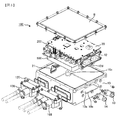
- FIG. 3 is an exploded perspective view of the power conversion apparatus 100 as an embodiment according to the present invention.
- the power conversion device 100 includes a housing 10 and a cover 8 for fixing and protecting the power conversion module 200 with a power conversion module 200 described later as a core, and connection with an external device is performed by connecting a DC power supply input unit and an AC power supply.
- a connector module 120 that is an output section of the control unit, a signal connector 21 that transmits a signal to the control circuit, and an inlet pipe 13 and an outlet pipe 14 for introducing and discharging the cooling medium to and from the flow path forming body 12.
- the flow path forming body 12 and the housing 10 are separate parts as illustrated.
- the power converter 100 Since the power converter 100 has a substantially rectangular shape at the bottom and top surfaces, it can be easily attached to the vehicle and can be easily produced.
- the direction from the bottom surface of the housing 10 to the cover 8 is upward, the opposite is downward, and the vertical direction is the height direction.
- the flow path forming body 12 holds components such as a power semiconductor module 300, a smoothing capacitor module 500, a first AC bus bar 801, and the circuit board 20 described later, and cools them with a cooling medium.
- the housing 10 houses circuit components constituting the power conversion module 200, and an opening is provided in the side wall of the housing 10, and the signal connector 21 is fixed.
- the signal connector 21 is connected to an external control device through the opening, and signal transmission is performed between the control circuit 172 provided on the circuit board 20 and an external control device such as a host control device.
- Low voltage DC power for operating the control circuit in the power converter 100 is supplied from the signal connector 21.
- a connector module 120 for connecting an external device and a direct current and an alternating current power source is fixed to another opening provided on the side wall of the housing 10.
- the connector module 120 is provided with a DC connector portion 138 for transmitting and receiving DC power to and from the battery 136, and a negative power line 139 b and a positive electrode for supplying high voltage DC power to the power converter 100.
- the side power line 139a electrically connects the battery 136 and the smoothing capacitor module 500 or the like.
- the connector module 120 is provided with an AC connector portion 188 for transmitting and receiving an AC current between the motor generator and the power semiconductor module 300, and an AC wiring 189a for supplying high voltage AC power to the motor generator.
- ⁇ 189c electrically connect the motor generator and the power semiconductor modules 300a to 300c.
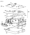
- FIG. 4 is an exploded perspective view for assisting understanding of the components and the water channel configuration incorporated in the flow path forming body 12 which is a component of the power conversion module 200.
- the flow path forming body 12 has a smaller size in the vertical direction than the dimensions in the other directions and has a flat shape, and an outlet connecting the inlet pipe connection portion 12a and the outlet pipe 14 on the side surface.
- a pipe connecting portion 12b is provided, and the cooling flow path 19 is formed in a U shape so as to connect two pipes.
- the upper surface on one side of the cooling flow path 19 is open.
- the cooling medium flows from the inlet pipe 13, and the flow path 19a into which the power semiconductor module 300a is inserted, the flow path 19b into which the power semiconductor module 300b is inserted, the folded flow path portion 19c, and the flow path into which the power semiconductor module 300c is inserted. It is discharged from the outlet pipe 14 through 19d and the flow path 19e.
- the opening surface 400 is closed by the flow path cover 420 and the flow path cover seal member 405. Further, openings 402a to 402c are formed on the side surface of the flow path forming body 12 along the flow of the refrigerant.
- the openings 402a to 402c are closed by the inserted power semiconductor modules 300a to 300c and the flange seal members 406a to 406c, and the power semiconductor modules 300a to 300c are cooled by the cooling medium flowing through the cooling flow path 19. That is, the power semiconductor modules 300a to 300c are inserted into the cooling channel 19 through the openings 402a to 402c in a direction perpendicular to the flow direction of the cooling medium flowing through the cooling channel 19.
- the power radiating surface 307A and the second radiating surface 307B, which will be described later, in the power semiconductor modules 300a to 300c are parallel to the upper surface and the lower surface of the flow path forming body 12, respectively.
- the semiconductor modules 300a to 300c are cooled.
- the minimum dimension in the height direction of the flow path forming body 12 that houses the power semiconductor module 300 (the minimum distance between the top surface and the bottom surface of the flow path forming body 12) is the power semiconductor module 300. Therefore, the height of the flange 304B, which will be described later, can be reduced to a height obtained by adding the plate thickness of the flow path cover 420 to the width.
- the folded flow path portion 19c is provided in the flow path, and the flexibility of layout of the power semiconductor modules 300a to 300c is increased without deteriorating the cooling performance. Miniaturization is also possible.
- the power semiconductor modules 300a and 300b are provided in the cooling flow path 19 in the refrigerant flow direction 418a, which is the forward path
- the power semiconductor module 300c is provided in the cooling flow path 19 in the refrigerant flow direction 418c, which is the return path. .
- the cooling channel 19 has an effect of increasing the mechanical strength in addition to the cooling effect by making the main structure of the cooling channel 19 of the channel forming body 12 integrally with the channel forming body 12 by casting aluminum. . Moreover, the flow path forming body 12 and the cooling flow path 19 are integrated with each other by being made by aluminum casting, heat conduction is improved, and cooling efficiency is improved.
- the power semiconductor modules 300a to 300c are fixed to the cooling channel 19 to complete the cooling channel 19, and a water leak test is performed on the water channel.
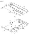
- FIG. 5 is an exploded perspective view for helping understanding the configuration of the power conversion module 200.
- a power semiconductor module 300 is accommodated in the flow path forming body 12.
- the smoothing capacitor module 500 is assembled at a position close to the lower surface of the flow path forming body 12.
- the flow path 19e portion can suppress the depth of the flow path.
- the lower surface has a recessed shape, and a resistor 450 is fixed to the recessed portion.
- a current sensor 180 is fixed with a boss, and a bus bar assembly 800 is also fixed.
- the bus bar assembly 800 includes bus bar bodies 801a, 801b and 801c that transmit AC power, a heat transfer member 803, and a bus bar holding member 802.
- the bus bar assembly 800 is fixed to the flow path cover 420 at the lower part, and the circuit at the upper part. It is fixed to the substrate 20.
- the terminals provided on the smoothing capacitor module 500 and the AC bus bars 801a to 800c are electrically connected to the power semiconductor modules 300a to 300c, and the connecting portions are joined by welding.
- the heat generating components can be arranged close to both the upper surface and the lower surface, that is, the surface having a large area. In contrast, the cooling efficiency is greatly improved.
- the area that can be used for the layout of the smoothing capacitor module 500 can be the same area as that of the flow path forming body 12, the dimension in the height direction is suppressed while ensuring the capacitor capacity necessary for ensuring the inverter performance. Can be reduced in height.
- the board of the driver circuit 174 and the board of the control circuit 172 cannot be arranged on the same plane.
- the driver circuit 174 and the control circuit 172 can be arranged on the same circuit board 20 and the height can be reduced.
- the assembly work including welding is performed by the power conversion module 200. This is possible from all directions, and as a result, the degree of freedom in design is increased, so that it is possible to reduce the size and cost, and the productivity is improved in the production department.
- the inspection can be performed in the state of the power conversion module 200 at the production site.
- the parts such as the housing 10 are not discarded, the yield can be reduced.
- FIG. 6 illustrates a means for fixing the flow path forming body 12 to the housing 10.
- FIG. 6A is a cross-sectional view of the vicinity of the inlet pipe 13 and the outlet pipe 14.
- FIG. 6B is a cross-sectional view of the facing side of the surface to which the inlet / outlet pipe is attached.
- the flow path forming body 12 is provided with an inlet pipe connecting portion 12a and an outlet pipe connecting portion 12b shown in FIG. 4, and a flange 12c including both the connecting portions is formed.
- the inlet pipe connection part 12a and the outlet pipe connection part 12b connect the cooling flow path 19 of the flow path forming body 12 and an external device.
- the housing 10 is provided with an opening 10a matched to the flow path forming body flange 12c.
- the flange 12 c including the inlet pipe connecting portion 12 a and the outlet pipe connecting portion 12 b is exposed to the outside of the housing 10 through the opening 10 a formed in the housing 10.
- the cooling medium enters the flow path forming body 12 directly from the inlet pipe 13, passes through the cooling flow path 19, and is discharged from the direct outlet pipe 14.
- the required specification for the housing 10 is lower than that of the conventional housing.
- the housing is machined or impregnated in order to prevent leakage of the cooling medium.
- an alternative material such as resin can be selected for the housing 10, it is possible to reduce the weight and reduce the cost.
- An internal thread is provided on the flange 12c provided on the flow path forming body 12 described above, and after the seal member 407 matched to the flange shape is assembled, the fastening screw 31 is used to make a perpendicular to the flange 12c. It is fixed to the housing 10 by tightening from the direction.
- the housing 10 is provided with a female screw 10c on the opposite side of the surface to which the inlet / outlet pipe is attached, and the flange 12e of the flow path forming body 12 is fastened in the vertical direction using the fastening screw 32. .
- a support portion 12d is provided at the lower portion of the flange 12c, and a support portion 10b is provided on the opposite housing 10 so that the load in the vertical direction is received by the indication portion 12d and the support portion 10, and a fastening screw 31 has the function of suppressing the stress in the shearing direction generated at 31.
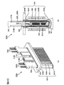
- FIG. 7 describes the flow path cover 420 to help understanding.
- FIG. 7A is a perspective view of the flow path cover 420 as viewed from the side in contact with the opening surface 400 of the flow path forming body 12.
- the flow path cover 420 is provided with a convex portion 420a in accordance with the cooling flow path 19 and the power semiconductor module 300, so that the clearance with the heat radiating portion provided in the power semiconductor module 300 can be made uniform and appropriate. Will improve.
- FIG. 7B is a perspective view of the flow path cover 420 as viewed from the upper surface of the flow path forming body 12.
- the flow path cover 420 has a shape 420b that is recessed according to the convex portion 420a, and an AC bus bar holding member mounting boss 420c is provided in the recessed portion. Since the mounting boss 420c is provided in the recessed portion, the height of the boss can be suppressed and the height can be reduced.
- a circuit board mounting boss 420d is provided on the surface of the flow path cover 420 shown in FIG. Since the mounting boss 420d can be arranged at an arbitrary position, the distance between the support points when mechanical vibration occurs can be shortened, and the resonance frequency can be increased, thereby improving the reliability. In addition, since the flow path cover 420 is located between the power semiconductor module 300 and the circuit board 20, an electromagnetic shielding effect can be obtained. In the conventional configuration, a dedicated metal plate is used, but in the present embodiment, since it can be integrated into the flow path cover 420, there is an effect of cost reduction. If the effect of electromagnetic shielding / board cooling is low, electromagnetic shielding / board cooling can be achieved by placing a thin conductive metal plate between the bus bar assembly 800 and the circuit board 20. However, the effect of cost reduction can be obtained.
- the power semiconductor modules 300a to 300c have the same structure, and the structure of the power semiconductor module 300a will be described as a representative. 7 to 11, the signal terminal 325U corresponds to the gate electrode 154 and the signal emitter electrode 155 disclosed in FIG. 2, and the signal terminal 325L corresponds to the gate electrode 164 and the emitter electrode 165 disclosed in FIG. To do.
- the DC positive terminal 315B is the same as the positive terminal 157 disclosed in FIG. 2, and the DC negative terminal 319B is the same as the negative terminal 158 disclosed in FIG.
- the AC terminal 321 is the same as the AC terminal 159 disclosed in FIG.
- FIG. 8A is a perspective view in which the terminal shape is changed so that the power semiconductor module 300a of the present embodiment can be easily explained.
- FIG. 8B is a cross-sectional view of the power semiconductor module 300a of this embodiment.
- the power semiconductor elements (IGBT 328, IGBT 330, diode 156, and diode 166) constituting the series circuit 150 of the upper and lower arms are connected by the conductor plate 315 or the conductor plate 318 or the conductor plate 316 or the conductor plate as shown in FIGS. By 319, it is fixed by being sandwiched from both sides.
- These conductor plates are assembled with an auxiliary molded body 600 formed by integrally molding the signal wirings which are the signal terminals 325U and 325L.
- the conductor plate 315 and the like are sealed with the first sealing resin 348 with the heat dissipation surface exposed, and the insulating sheet 333 is thermocompression bonded to the heat dissipation surface.
- the module primary sealing body 302 sealed with the first sealing resin 348 is inserted into the module case 304 and sandwiched with the insulating sheet 333, and is thermocompression bonded to the inner surface of the module case 304 that is a CAN type cooler.
- the CAN-type cooler is a cylindrical cooler having an insertion port 306 on one surface and a bottom on the other surface.
- the module case 304 is made of an aluminum alloy material such as Al, AlSi, AlSiC, Al—C, etc., and is formed by joining one or a plurality of parts.
- the module case 304 has a structure in which no opening other than the insertion port 306 is provided.
- the insertion port 306 is surrounded by a flange 304B.
- the first heat radiating surface 307A and the second heat radiating surface 307B which are wider than the other surfaces, are arranged facing each other, and the facing first heat radiating surface 307A and The three surfaces connected to the second heat radiating surface 307B constitute a surface sealed with a narrower width than the first heat radiating surface 307A and the second heat radiating surface 307B, and the insertion port 306 is formed on the other side surface.
- the shape of the module case 304 does not have to be an accurate rectangular parallelepiped, and the corners may form a curved surface as shown in FIG.
- the metallic case having such a shape By using the metallic case having such a shape, even when the module case 304 is inserted into the cooling channel 19 through which a coolant such as water or oil flows, a seal against the coolant can be secured by the flange 304B. It is possible to prevent the medium from entering the inside of the module case 304 with a simple configuration. Further, the fins 305 are uniformly formed on the first heat radiation surface 307A and the second heat radiation surface 307B facing each other.
- a curved portion 304A having an extremely thin thickness is formed on the outer periphery of the first heat radiating surface 307A and the second heat radiating surface 307B. Since the curved portion 304A is extremely thin to such an extent that it can be easily deformed by pressurizing the fin 305, the productivity after the module primary sealing body 302 is inserted is improved.
- the gap remaining inside the module case 304 is filled with the second sealing resin 351. Further, as shown in FIGS. 9 and 10, a DC positive electrode wiring 315A and a DC negative electrode wiring 319A for electrical connection with the smoothing capacitor module 500 are provided, and a DC positive electrode terminal 315B (157) is provided at the tip thereof. ) And a DC negative terminal 319B (158). An AC wiring 320 for supplying AC power to the motor generator or 194 is provided, and an AC terminal 321 (159) is formed at the tip thereof.
- the DC positive electrode wiring 315A is integrally formed with the conductor plate 315
- the DC negative electrode wiring 319A is integrally formed with the conductor plate 319
- the AC wiring 320 is integrally formed with the conductor plate 316.
- the gap between the conductor plate and the inner wall of the module case 304 can be reduced, and the power semiconductor element The generated heat can be efficiently transmitted to the fins 305.
- the generation of thermal stress can be absorbed by the insulating sheet 333, which is favorable for use in a power conversion device for a vehicle having a large temperature change. .
- FIG. 9A is an internal cross-sectional view in which the module case 304, the insulating sheet 333, the first sealing resin 348, and the second sealing resin 351 are removed in order to help understanding.
- FIG. 9B is an internal perspective view.
- FIG. 10 (a) is an exploded view for helping understanding of the structure of FIG. 9 (b).
- FIG. 10B is a circuit diagram of the power semiconductor module 300.
- FIG. 11A is a circuit diagram for explaining the inductance reduction effect
- FIG. 11B is a perspective view showing a current flow for explaining the inductance reduction effect.
- the direct current positive electrode side conductor plate 315 and the alternating current output side conductor plate 316 are arranged in substantially the same plane.
- the collector electrode of the IGBT 328 on the upper arm side and the cathode electrode of the diode 156 on the upper arm side are fixed.
- the collector electrode of the IGBT 330 on the lower arm side and the cathode electrode of the diode 166 on the lower arm side are fixed.
- the AC conductor plate 318 and the conductor plate 319 are arranged in substantially the same plane.
- the emitter electrode of the IGBT 328 on the upper arm side and the anode electrode of the diode 156 on the upper arm side are fixed.
- an emitter electrode of the IGBT 330 on the lower arm side and an anode electrode of the diode 166 on the lower arm side are fixed.
- Each power semiconductor element is fixed to an element fixing portion 322 provided on each conductor plate via a metal bonding material 160.
- the metal bonding material 160 is, for example, a low-temperature sintered bonding material including a solder material, a silver sheet, and fine metal particles.
- Each power semiconductor element has a flat plate-like structure, and each electrode of the power semiconductor element is formed on the front and back surfaces. As shown in FIG. 9A, each electrode of the power semiconductor element is sandwiched between the conductor plate 315 and the conductor plate 318, or the conductor plate 316 and the conductor plate 319. In other words, the conductor plate 315 and the conductor plate 318 are stacked so as to face each other substantially in parallel via the IGBT 328 and the diode 156. Similarly, the conductor plate 316 and the conductor plate 319 have a stacked arrangement facing each other substantially in parallel via the IGBT 330 and the diode 166. Further, the conductor plate 316 and the conductor plate 318 are connected via an intermediate electrode 329. By this connection, the upper arm circuit and the lower arm circuit are electrically connected to form an upper and lower arm series circuit.
- the direct current positive electrode wiring 315A and the direct current negative electrode wiring 319A have a shape extending substantially in parallel while facing each other through an auxiliary mold body 600 formed of a resin material.
- the signal terminal 325U and the signal terminal 325L are formed integrally with the auxiliary mold body 600 and extend in the same direction as the DC positive electrode wiring 315A and the DC negative electrode wiring 319A.
- a thermosetting resin having an insulating property or a thermoplastic resin is suitable.
- the direct current positive electrode wiring 315A and the direct current negative electrode wiring 319A are arranged so as to face each other substantially in parallel, so that currents that instantaneously flow during the switching operation of the power semiconductor element face each other in the opposite direction. As a result, the magnetic fields produced by the currents cancel each other out, and this action can reduce the inductance.
- the lower arm side diode 166 is in a conductive state in a forward bias state. In this state, when the upper arm side IGBT 328 is turned on, the diode 166 on the lower arm side is reversely biased, and a recovery current caused by carrier movement passes through the upper and lower arms.
- a recovery current 360 shown in FIG. 11B flows through each of the conductor plates 315, 316, 318, and 319. As indicated by the dotted line, the recovery current 360 passes through the DC positive terminal 315B (157) disposed opposite to the DC negative terminal 319B (158), and is subsequently formed by the conductor plates 315, 316, 318, and 319. It flows through the loop-shaped path, and again flows as shown by the solid line through the DC negative terminal 319B (158) arranged opposite to the DC positive terminal 315B (157).
- the eddy current 361 flows through the first heat radiating surface 307A and the second heat radiating surface 307B of the module case 304 by the current flowing through the loop-shaped path. Due to the magnetic field canceling effect generated by the equivalent circuit 362 in the current path of the eddy current 361, the wiring inductance 363 in the loop-shaped path is reduced.
- the loop-shaped current path flows through a path close to the DC positive terminal 315B (157) side of the conductor plate 315 and passes through the IGBT 328 and the diode 156 as indicated by a dotted line.
- the loop-shaped current path flows through a path farther from the DC positive terminal 315B (157) side of the conductor plate 318 as shown by the solid line, and then farther from the DC positive terminal 315B (157) side of the conductor board 316 as shown by the dotted line.
- the path flows through the IGBT 330 and the diode 166.
- the loop-shaped current path flows along a path close to the DC negative electrode wiring 319A side of the conductor plate 319.
- the loop-shaped current path passes through a path closer to or farther from the DC positive terminal 315B (157) or the DC negative terminal 319B (158), thereby forming a current path closer to the loop shape. Is done.
- FIG. 12 (a) is a perspective view of the auxiliary mold body 600
- FIG. 12 (b) is a transparent view of the auxiliary mold body 600.
- the auxiliary mold body 600 has the signal conductor 324 integrated by insert molding.
- the signal conductor 324 receives the temperature information of the upper arm side gate electrode terminal 154 and the emitter electrode terminal 155, the upper arm side gate electrode terminal 164 and the emitter electrode terminal 165 (see FIG. 2), and the power semiconductor element.
- a terminal for transmission is included. In the description of this embodiment, these terminals are collectively referred to as signal terminals 325U and 325L.
- the signal conductor 324 forms signal terminals 325U and 325L at one end, and forms element-side signal terminals 326U and 326L at the other end.
- the element-side signal terminals 326U and 326L are connected to signal pads provided on the surface electrode of the power semiconductor element by, for example, wires.
- the first sealing portion 601A has a shape extending in a direction transverse to the major axis of the shape of the DC positive electrode wiring 315A, the DC negative electrode wiring 319A, or the AC wiring 320 shown in FIG.
- the second sealing portion 601B has a shape extending in a direction substantially parallel to the major axis of the shape of the DC positive electrode wiring 315A, the DC negative electrode wiring 319A, or the AC wiring 320.
- the second sealing portion 601B includes a sealing portion for sealing the signal terminal 325U on the upper arm side and a sealing portion for sealing the signal terminal 325L on the lower arm side.
- the auxiliary mold body 600 is formed so that its length is longer than the entire length of the conductor plates 315 and 316 arranged side by side or the entire length of the conductor plates 319 and 320 arranged side by side. That is, the lengths of the conductor plates 315 and 316 arranged side by side or the lengths of the conductor plates 319 and 320 arranged side by side are within the range of the lateral length of the auxiliary mold body 600.
- the first sealing portion 601A has a hollow shape and forms a wiring fitting portion 602B for fitting the DC negative electrode wiring 319A into the hollow.
- the first sealing portion 601A has a hollow shape and forms a wiring fitting portion 602A for fitting the DC positive electrode wiring 315A into the hollow.
- the first sealing portion 601A is disposed on the side of the wiring fitting portion 602A, has a hollow shape, and further forms a wiring fitting portion 602C for fitting the AC wiring 320 into the hollow. To do.
- Each wiring is positioned by fitting each wiring to these wiring fitting portions 602A to 602C. Thereby, it becomes possible to perform the filling operation of the resin sealing material after firmly fixing each wiring, and the mass productivity is improved.
- the wiring insulation part 608 protrudes in a direction away from the first sealing part 601A from between the wiring fitting part 602A and the wiring fitting part 602B. Since the plate-shaped wiring insulating portion 608 is interposed between the DC positive electrode wiring 315A and the DC negative electrode wiring 319A, it is possible to arrange the wiring insulating portion 608 so as to reduce the inductance while ensuring insulation.
- the first sealing portion 601A is formed with a mold pressing surface 604 that comes into contact with a mold used for resin sealing, and the mold pressing surface 604 prevents resin leakage during resin sealing.
- a protruding portion 605 for preventing is formed around the outer periphery in the longitudinal direction of the first sealing portion 601.
- a plurality of protrusions 605 are provided to enhance the resin leakage prevention effect.
- the protrusions 605 are also provided in the wiring fitting part 602A and the wiring fitting part 602B, it is possible to prevent the resin sealing material from leaking from the periphery of the DC positive electrode wiring 315A and the DC negative electrode wiring 319A.
- the material of the first sealing portion 601A, the second sealing portion 601B, and the protrusion 605 is a heat that can be expected to have high heat resistance in consideration of being installed in a mold of about 150 to 180 ° C.
- a liquid crystal polymer of plastic resin, polybutylene terephthalate (PBT) or polyphenylene sulfide resin (PPS) is desirable.
- a plurality of through holes 606 shown in FIG. 12B are provided in the longitudinal direction on the power semiconductor element side in the short direction of the first sealing portion 601A.
- the first sealing resin 348 flows into the through-hole 606 and hardens, whereby an anchor effect is exerted, and the auxiliary mold body 600 is firmly held by the first sealing resin 348, and temperature changes and machine Even if stress is applied by mechanical vibration, both do not peel off. It is difficult to peel even if the shape is uneven instead of the through hole.
- a certain degree of effect can be obtained by applying a polyimide coating agent to the first sealing portion 601A or roughening the surface.
- the auxiliary mold body 600 supporting each wiring is inserted into a mold preheated to about 150 to 180 ° C.
- the auxiliary mold body 600, the direct current positive electrode wiring 315A, the direct current negative electrode wiring 319A, the alternating current wiring 320, the conductor plate 315, the conductor plate 316, the conductor plate 318, and the conductor plate 319 are firmly connected to each other.
- the second sealing portion 601B is formed to extend from the vicinity of the module case 304 to the vicinity of the driver circuit board.
- the switching control signal can be normally transmitted even when exposed to a high voltage.
- the DC positive wiring 315A, the DC negative wiring 319A, the AC wiring 320, the signal terminal 325U, and the signal terminal 325L protrude from the module case 304 in the same direction, it is possible to ensure electrical insulation and ensure reliability. it can.
- FIG. 13 is an exploded perspective view for explaining the internal structure of the smoothing capacitor module 500.
- the laminated conductor plate 501 is composed of a negative electrode conductor plate 505 and a positive electrode conductor plate 507 formed of plate-like wide conductors, and an insulating sheet (not shown) sandwiched between the negative electrode conductor plate 505 and the positive electrode conductor plate 507. .
- the laminated conductor plate 501 cancels out the magnetic flux with respect to the current flowing through the series circuit 150 of the upper and lower arms of each phase, so that the inductance of the current flowing through the series circuit 150 of the upper and lower arms is reduced.
- the laminated conductor plate 501 has a substantially square shape.
- the negative power supply terminal 508 and the positive power supply terminal 509 are formed so as to rise from one side of the laminated conductor plate 501 and are connected to the positive conductor plate 507 and the negative conductor plate 505, respectively.
- DC power is supplied to the positive power supply terminal 509 and the negative power supply terminal 508 via the DC connector 138 as described with reference to FIG.
- the capacitor terminal 503c is raised from the same side as the negative power supply terminal 508 and the positive power supply terminal 509, and the capacitor terminals 503a and 503b are raised from opposite sides of the capacitor terminal 503c. It is formed corresponding to the positive terminal 157 (315B) and the negative terminal 158 (319B) of the semiconductor module 300. Capacitor terminals 503a to 503c are connected to power semiconductor modules 300a to 300c, respectively. A part of an insulating sheet (not shown) is provided between the negative-side capacitor terminal 504a and the positive-side capacitor terminal 506a constituting the capacitor terminal 503a to ensure insulation. The same applies to the other capacitor terminals 503b and 503c.
- the negative electrode conductor plate 505, the positive electrode conductor plate 507, the battery negative electrode side terminal 508, the battery negative electrode side terminal 509, and the capacitor terminals 503a to 503f are composed of integrally formed metal plates, and the upper and lower arms This has the effect of reducing the inductance with respect to the current flowing through the series circuit 150.
- a plurality of capacitor cells 514 are provided on the inner side of the smoothing capacitor module 500 below the laminated conductor plate 501.
- four capacitor cells 514 are arranged in a line along one side of multilayer conductor plate 501, and another twelve capacitor cells 514 are along the other side of multilayer conductor plate 501.
- a total of 16 capacitor cells are provided.
- the refrigerant flow path is provided in the state close to the upper surface of the smoothing capacitor module 500, and the cooling efficiency is improved.
- Capacitor cell 514 is a unit structure of a power storage unit of smoothing capacitor module 500, and two films each having a metal such as aluminum deposited thereon are stacked and wound to form a positive electrode and a negative electrode, respectively. Use a film capacitor.
- the electrode of the capacitor cell 514 is manufactured by spraying a conductor such as tin, with the wound shaft surfaces serving as a positive electrode and a negative electrode, respectively.
- the capacitor case 502 includes a storage portion 511 for storing the capacitor cell 514, and the storage portion 511 has a substantially rectangular upper surface and lower surface shown in the drawing.
- the capacitor case 502 is provided with fixing means for fixing the smoothing capacitor module 500 to the flow path forming body 12, for example, holes 520a to 520d for allowing screws to pass therethrough.
- the bottom surface portion 513 of the storage portion 511 has a smooth uneven shape or corrugated shape so as to match the surface shape of the cylindrical capacitor cell 514. This facilitates positioning of the module in which the laminated conductor plate 501 and the capacitor cell 514 are connected to the capacitor case 502.
- the capacitor case 502 is filled with a filler (not shown). Since the bottom surface portion 513 has a corrugated shape in accordance with the shape of the capacitor cell 514, the capacitor cell 514 can be prevented from being displaced from a predetermined position when the filler is filled in the capacitor case 502.
- the capacitor cell 514 generates heat due to a ripple current at the time of switching due to the electric resistance of the metal thin film and the internal conductor deposited on the internal film. Therefore, in order to easily release the heat of the capacitor cell 514 through the capacitor case 502, the capacitor cell 514 is molded with a filler. Furthermore, the moisture resistance of the capacitor cell 514 can be improved by using a resin filler.
- the tip of the AC terminal 321 (159) of the power semiconductor module 300 is connected to the tips of the AC bus bars 801a to 801c by welding.
- the bus bar assembly 800 includes AC bus bars 801a to 801c, a heat transfer member 803, and a bus bar holding member 802.
- the AC bus bars 801a to 801c and the heat transfer member 803 are fixed to the flow path cover 420 by the bus bar holding member 802. Since heat generated by energization of the AC bus bars 801a to 801c is transmitted to the flow path forming body 12 via the heat transfer member 803, there is an effect of cooling the AC bus bars 801a to 801c.
- FIG. 14 is a perspective view disassembled into components for explaining the overall configuration of the connector module 120.
- DC bus bars 814 a and 814 b are held by a DC bus bar holding member 818 and fixed to the connector housing 121. One ends of the DC bus bars 814 a and 814 b are respectively connected to the positive power terminal 509 and the negative power terminal 508 provided in the smoothing capacitor module 500.
- the second AC bus bars 804 a to 804 c are held by an AC bus bar holding member 817 and fixed to the connector housing 121. One ends of the second AC bus bars 804a to 804c are connected to the first AC bus bars 801a to 801c included in the power conversion module 200, respectively.
- the other ends of the DC bus bars 814a and 814b and the second AC bus bars 804a to 804c are generally connected to a DC wiring 139 and an AC wiring 189 provided on the vehicle side.
- the DC bus bar 814 and the DC wiring 139 are fastened with the fastening screw 36 shown in FIG. 15 and sealed with the DC connector cover 822.
- the AC wiring 189 is inserted into the AC connector portion 188 of the connector housing 121
- the second AC bus bar 804 and the AC wiring 189 are fastened with the fastening screw 35 shown in FIG. 15 and sealed with the AC connector cover 821. It is configured to do.
- the connector module 120 has the DC connector portion 138 and the AC connector portion 188 integrated, but each connector module 120 may be separately manufactured and fixed to the housing 10.
- the connection between the DC wiring 139 and the AC wiring 189 is fastened with a screw.
- the above-described effect can be obtained in the same manner by using a metal spring force to ensure electrical contact.
- FIG. 15 is a view from the top surface of the power converter 100 with the cover 8 removed.
- FIG. 16 is a perspective view showing parts easily attached to the side surface of the power conversion apparatus 100 shown in FIG.
- the components are assembled in a module state, and are fixed to the housing 10 with fastening screws 31 and 32.
- the fastening screw 32 performs a fastening operation from the opening of the housing 10, and the fastening screw 31 performs a fastening operation from the external side surface.
- the fixing position of the housing 10 to the vehicle can be freely set. It is possible to obtain effects such as cost reduction of molds when manufacturing, standardization of production equipment, and reduction of design man-hours.
- the inlet pipe 13, the outlet pipe 14, the connector module 120, and the signal connector 21 are fastened with fastening screws 33, 34, and 37, and the DC bus bar 814 and the power terminals 508 and 509 are fastened with the fastening screws 36.
- the 1 AC bus bar 801 and the second AC bus bar 804 are connected by the fastening screw 35.
- the board connector 38 of the signal connector 21 into the circuit board 20, the connection of each part is completed.
- only the cooling medium connection pipes 13 and 14, the signal connector 21, the DC connector part 138, and the AC connector part 188 that are interfaces with external devices are changed. Since a wide range of measures can be taken, effects such as standardization of parts, cost reduction of molds of component parts, standardization of production facilities, reduction of design man-hours, and the like can be obtained.
- FIG. 17 is a cross-sectional view of the flow path forming body and the cooling medium passage of the power semiconductor module 300.
- FIG. 17A is a cross-sectional view of a conventional configuration
- FIG. 17B is a cross-sectional view of the present embodiment.
- the flow path forming body generally uses die-cast aluminum in consideration of strength, heat dissipation, sealing performance of the cooling refrigerant, cost, and the like. Die casting is a manufacturing method in which molten aluminum is injected into a metal mold at a high pressure, and the product is taken out of the mold after cooling. Therefore, the surface parallel to the mold drawing direction is tapered so that the mold and the product can be easily separated when the product is taken out.
- the power semiconductor module 300 is inserted from the upper surface of the flow path forming body 901, and the lower surface of the flow forming body 901 is sealed by the lower cover 902. Yes.
- the die is drawn in the direction of the upper die casting die 912 and the lower die casting die 913 with the die dividing surface 911 as a boundary.
- a tapered surface 914 is required.
- the clearance 916 between the heat radiation fin 305 and the tapered surface 914 provided in the power semiconductor module 300 differs depending on the location.
- the cooling refrigerant passes through a large portion, the cooling performance is non-uniform, and there is a concern that the performance of the power semiconductor module 300 may be reduced.
- the taper surface 914 can be machined to make the clearance 916 uniform. However, since machining is required, this has been a factor in increasing costs.
- the power semiconductor module 300 is inserted from the side surface of the flow path forming body 12, and the upper surface of the flow path forming body 12 is sealed with the flow path cover 420. It is configured to be stopped.
- the die is drawn in the upward die casting direction 922.
- the tapered surface 924 which is a surface parallel to the drawing direction is close to the side surface of the power semiconductor module 300 which is a surface perpendicular to the heat radiation fin 305 of the power semiconductor module 300.
- the surface close to the heat radiation fin 305 provided in the power semiconductor module 300 becomes a surface 925 that does not require a taper, so that a uniform and minimum clearance 926 can be secured. This can improve the performance of the power semiconductor module 300 and can reduce the cost because machining is unnecessary.
- the power conversion device described in the above-described embodiment and the system using this device solve various problems that are desired to be solved for commercialization.
- One of the various problems solved by these embodiments is an improvement in productivity.
- the above problem can be solved not only by the configuration described above but also by other configurations.
- a power semiconductor module is inserted from the side of the refrigerant passage, a smoothing capacitor module is arranged on the lower surface of the refrigerant passage, an AC bus bar and a circuit board are arranged on the upper surface of the refrigerant passage. It has a configuration in which it is modularized, the module is assembled to a housing, and electrical wiring, refrigerant piping, and signal wiring are assembled.
- the entire configuration of the power conversion device can be arranged in a more orderly manner, and the power conversion device can be reduced in size. Further, it is possible to obtain a low profile effect that can further reduce the size of the power converter in the lateral direction across the refrigerant flow path.
- a flow path forming body that forms a refrigerant flow path is provided along the upper surface of the smoothing capacitor module, and the smoothing capacitor module is fixed to the flow path forming body so that the power flow is increased by the refrigerant flow path.
- the semiconductor module and the smoothing capacitor module can be cooled together. Further, since the AC bus bar and the circuit board can be arranged close to the refrigerant passage side, cooling can be performed efficiently.
Abstract
La présente invention concerne un convertisseur de puissance comprenant : un module semi-conducteur de puissance ; un module de condensateur de lissage ; une barre omnibus pour courant alternatif ; un circuit de commande destiné à commander un élément semi-conducteur de puissance ; et un corps formant trajet d'écoulement, qui forme un trajet d'écoulement dans lequel circule un réfrigérant. Le module semi-conducteur de puissance possède une première partie de dissipation thermique et une seconde partie de dissipation thermique qui fait face à la première partie de dissipation thermique. La partie extérieure du corps formant trajet d'écoulement possède une première paroi qui fait face à la première partie de dissipation thermique, avec le trajet d'écoulement entre elles, une seconde paroi qui fait face à la seconde partie de dissipation thermique, avec le trajet d'écoulement entre elles, et une paroi latérale qui relie la première paroi et la seconde paroi. La paroi latérale possède une ouverture pour l'insertion du module semi-conducteur de puissance dans le trajet d'écoulement.
Priority Applications (4)
| Application Number | Priority Date | Filing Date | Title |
|---|---|---|---|
| EP12816900.0A EP2738930B1 (fr) | 2011-07-25 | 2012-07-25 | Convertisseur de puissance |
| US14/131,765 US9301434B2 (en) | 2011-07-25 | 2012-07-25 | Power conversion apparatus |
| EP14171862.7A EP2782433B1 (fr) | 2011-07-25 | 2012-07-25 | Appareil de conversion de puissance |
| CN201280036863.3A CN103733495B (zh) | 2011-07-25 | 2012-07-25 | 电力变换装置 |
Applications Claiming Priority (2)
| Application Number | Priority Date | Filing Date | Title |
|---|---|---|---|
| JP2011161533A JP5506749B2 (ja) | 2011-07-25 | 2011-07-25 | 電力変換装置 |
| JP2011-161533 | 2011-07-25 |
Publications (1)
| Publication Number | Publication Date |
|---|---|
| WO2013015319A1 true WO2013015319A1 (fr) | 2013-01-31 |
Family
ID=47601158
Family Applications (1)
| Application Number | Title | Priority Date | Filing Date |
|---|---|---|---|
| PCT/JP2012/068847 WO2013015319A1 (fr) | 2011-07-25 | 2012-07-25 | Convertisseur de puissance |
Country Status (5)
| Country | Link |
|---|---|
| US (1) | US9301434B2 (fr) |
| EP (2) | EP2782433B1 (fr) |
| JP (1) | JP5506749B2 (fr) |
| CN (1) | CN103733495B (fr) |
| WO (1) | WO2013015319A1 (fr) |
Cited By (2)
| Publication number | Priority date | Publication date | Assignee | Title |
|---|---|---|---|---|
| JP2015154634A (ja) * | 2014-02-17 | 2015-08-24 | 株式会社デンソー | 電力変換装置 |
| CN107785353A (zh) * | 2016-08-26 | 2018-03-09 | 阿尔斯通运输科技公司 | 包括改进的电气互连装置的电气开关设备 |
Families Citing this family (36)
| Publication number | Priority date | Publication date | Assignee | Title |
|---|---|---|---|---|
| JP5581131B2 (ja) * | 2010-06-30 | 2014-08-27 | 日立オートモティブシステムズ株式会社 | パワーモジュール及びそれを用いた電力変換装置 |
| FR2983360B1 (fr) * | 2011-11-25 | 2014-01-10 | Renault Sa | Dispositif de protection pour connecteur electrique d'un module d'electronique de puissance |
| JP5802629B2 (ja) * | 2012-08-31 | 2015-10-28 | 日立オートモティブシステムズ株式会社 | 電力変換装置 |
| JP5753829B2 (ja) * | 2012-09-28 | 2015-07-22 | 日立オートモティブシステムズ株式会社 | 電力変換装置 |
| JP5931778B2 (ja) * | 2013-02-28 | 2016-06-08 | 三菱重工業株式会社 | 電力変換モジュール結線用のバスバーアッセンブリ |
| JP6186143B2 (ja) | 2013-03-13 | 2017-08-23 | 日立オートモティブシステムズ株式会社 | 電力変換装置 |
| WO2014192394A1 (fr) * | 2013-05-31 | 2014-12-04 | アイシン・エィ・ダブリュ株式会社 | Dispositif de commande de véhicule |
| JP6236904B2 (ja) * | 2013-06-19 | 2017-11-29 | 株式会社デンソー | 電力変換装置 |
| JP5991345B2 (ja) * | 2013-12-26 | 2016-09-14 | 株式会社デンソー | 電力変換装置 |
| JP2015149883A (ja) * | 2014-01-09 | 2015-08-20 | 株式会社デンソー | 電力変換装置 |
| US10080313B2 (en) * | 2014-01-27 | 2018-09-18 | Hitachi, Ltd. | Power module and method for manufacturing the same |
| EP2990253B1 (fr) * | 2014-08-26 | 2017-03-29 | Visedo Oy | Module de condensateur pour machine de travail mobile |
| US10264695B2 (en) * | 2014-09-25 | 2019-04-16 | Hitachi Automotive Systems, Ltd. | Power converter |
| GB201503806D0 (en) * | 2015-03-06 | 2015-04-22 | Nissan Motor Mfg Uk Ltd | Intergrated Power Module |
| CN107466442B (zh) * | 2015-03-31 | 2019-08-20 | 日立汽车系统株式会社 | 电力变换装置 |
| CN106298688B (zh) * | 2015-05-28 | 2018-11-06 | 台达电子工业股份有限公司 | 封装型功率电路模块 |
| WO2017056686A1 (fr) * | 2015-09-30 | 2017-04-06 | 日立オートモティブシステムズ株式会社 | Dispositif de conversion de puissance |
| JP6488996B2 (ja) * | 2015-11-27 | 2019-03-27 | 株式会社デンソー | 電力変換装置 |
| JP6439750B2 (ja) * | 2016-05-20 | 2018-12-19 | 株式会社デンソー | 半導体装置 |
| KR101950442B1 (ko) * | 2017-04-28 | 2019-02-20 | 엘에스산전 주식회사 | 서브모듈 |
| JP6258543B2 (ja) * | 2017-05-22 | 2018-01-10 | 日立オートモティブシステムズ株式会社 | 電力変換装置 |
| CN109873567B (zh) * | 2017-12-04 | 2022-02-25 | 株式会社电装 | 电力变换装置 |
| KR102075415B1 (ko) * | 2018-01-29 | 2020-02-11 | 엘에스산전 주식회사 | 전동기 구동장치 |
| JP7111161B2 (ja) * | 2018-07-03 | 2022-08-02 | 日産自動車株式会社 | 電力変換ユニット |
| CN112470390A (zh) * | 2018-07-25 | 2021-03-09 | 株式会社电装 | 电源模块及电力转换装置 |
| JP6488421B1 (ja) * | 2018-09-12 | 2019-03-20 | 高周波熱錬株式会社 | スナバ回路及びパワー半導体モジュール並びに誘導加熱用電源装置 |
| JP2020141443A (ja) * | 2019-02-26 | 2020-09-03 | 本田技研工業株式会社 | パワーコントロールユニット |
| US11071240B2 (en) * | 2019-05-03 | 2021-07-20 | Hyundai Motor Company | Power converting apparatus |
| WO2021025300A1 (fr) * | 2019-08-07 | 2021-02-11 | Samsung Electronics Co., Ltd. | Dispositif électronique comportant une structure de boîte de blindage |
| CN111447755B (zh) * | 2020-04-15 | 2022-11-01 | 重庆宗申电子科技有限公司 | 一种控制器的制造装配方法 |
| JP2022160060A (ja) * | 2021-04-06 | 2022-10-19 | 三菱重工業株式会社 | 電気導体の冷却装置、電力変換装置及び回転電気機械 |
| JP7113937B1 (ja) * | 2021-04-15 | 2022-08-05 | 三菱電機株式会社 | 電力変換装置 |
| CN113163691B (zh) * | 2021-04-25 | 2023-03-10 | 江西威尔高电子股份有限公司 | 一种新能源汽车用嵌入式智能线路板 |
| KR20230026887A (ko) * | 2021-08-18 | 2023-02-27 | 현대자동차주식회사 | 모빌리티의 인버터 장치 |
| WO2024090838A1 (fr) * | 2022-10-25 | 2024-05-02 | 엘지이노텍 주식회사 | Dispositif de commande de moteur |
| CN116131047B (zh) * | 2023-04-04 | 2023-09-15 | 武汉嘉晨电子技术有限公司 | 一种汽车bdu电连接件、汽车bdu以及bdu散热方法 |
Citations (5)
| Publication number | Priority date | Publication date | Assignee | Title |
|---|---|---|---|---|
| JP2004312866A (ja) * | 2003-04-07 | 2004-11-04 | Nichicon Corp | インバータ装置 |
| JP2005516570A (ja) * | 2002-01-16 | 2005-06-02 | ロックウェル オートメーション テクノロジーズ, インコーポレーテッド | 複数の回路板を支持する小型流体冷却式電力コンバータ |
| JP2008193867A (ja) | 2007-02-07 | 2008-08-21 | Hitachi Ltd | 電力変換装置 |
| JP2010035347A (ja) * | 2008-07-29 | 2010-02-12 | Hitachi Ltd | 電力変換装置および電動車両 |
| JP2010258315A (ja) * | 2009-04-28 | 2010-11-11 | Hitachi Automotive Systems Ltd | パワーモジュール及び電力変換装置 |
Family Cites Families (14)
| Publication number | Priority date | Publication date | Assignee | Title |
|---|---|---|---|---|
| JPH03159710A (ja) | 1989-11-18 | 1991-07-09 | Brother Ind Ltd | 成形品 |
| US7187568B2 (en) * | 2002-01-16 | 2007-03-06 | Rockwell Automation Technologies, Inc. | Power converter having improved terminal structure |
| US6898072B2 (en) | 2002-01-16 | 2005-05-24 | Rockwell Automation Technologies, Inc. | Cooled electrical terminal assembly and device incorporating same |
| JP4756935B2 (ja) * | 2005-06-29 | 2011-08-24 | 本田技研工業株式会社 | コンデンサ搭載型インバータユニット |
| JP2007110778A (ja) * | 2005-10-11 | 2007-04-26 | Matsushita Electric Ind Co Ltd | モータ駆動装置および駆動方法 |
| JP4848187B2 (ja) * | 2006-01-17 | 2011-12-28 | 日立オートモティブシステムズ株式会社 | 電力変換装置 |
| JP4857017B2 (ja) * | 2006-04-27 | 2012-01-18 | 日立オートモティブシステムズ株式会社 | 電力変換装置 |
| JP4434181B2 (ja) * | 2006-07-21 | 2010-03-17 | 株式会社日立製作所 | 電力変換装置 |
| JP2008148530A (ja) * | 2006-12-13 | 2008-06-26 | Toshiba Corp | インバータ装置 |
| JP4452953B2 (ja) * | 2007-08-09 | 2010-04-21 | 日立オートモティブシステムズ株式会社 | 電力変換装置 |
| JP4580997B2 (ja) * | 2008-03-11 | 2010-11-17 | 日立オートモティブシステムズ株式会社 | 電力変換装置 |
| JP4708459B2 (ja) * | 2008-07-29 | 2011-06-22 | 日立オートモティブシステムズ株式会社 | 電力変換装置 |
| JP4988665B2 (ja) * | 2008-08-06 | 2012-08-01 | 日立オートモティブシステムズ株式会社 | 半導体装置および半導体装置を用いた電力変換装置 |
| WO2011083578A1 (fr) | 2010-01-08 | 2011-07-14 | トヨタ自動車株式会社 | Module semi-conducteur |
-
2011
- 2011-07-25 JP JP2011161533A patent/JP5506749B2/ja active Active
-
2012
- 2012-07-25 WO PCT/JP2012/068847 patent/WO2013015319A1/fr active Application Filing
- 2012-07-25 US US14/131,765 patent/US9301434B2/en active Active
- 2012-07-25 CN CN201280036863.3A patent/CN103733495B/zh active Active
- 2012-07-25 EP EP14171862.7A patent/EP2782433B1/fr active Active
- 2012-07-25 EP EP12816900.0A patent/EP2738930B1/fr active Active
Patent Citations (5)
| Publication number | Priority date | Publication date | Assignee | Title |
|---|---|---|---|---|
| JP2005516570A (ja) * | 2002-01-16 | 2005-06-02 | ロックウェル オートメーション テクノロジーズ, インコーポレーテッド | 複数の回路板を支持する小型流体冷却式電力コンバータ |
| JP2004312866A (ja) * | 2003-04-07 | 2004-11-04 | Nichicon Corp | インバータ装置 |
| JP2008193867A (ja) | 2007-02-07 | 2008-08-21 | Hitachi Ltd | 電力変換装置 |
| JP2010035347A (ja) * | 2008-07-29 | 2010-02-12 | Hitachi Ltd | 電力変換装置および電動車両 |
| JP2010258315A (ja) * | 2009-04-28 | 2010-11-11 | Hitachi Automotive Systems Ltd | パワーモジュール及び電力変換装置 |
Non-Patent Citations (1)
| Title |
|---|
| See also references of EP2738930A4 |
Cited By (2)
| Publication number | Priority date | Publication date | Assignee | Title |
|---|---|---|---|---|
| JP2015154634A (ja) * | 2014-02-17 | 2015-08-24 | 株式会社デンソー | 電力変換装置 |
| CN107785353A (zh) * | 2016-08-26 | 2018-03-09 | 阿尔斯通运输科技公司 | 包括改进的电气互连装置的电气开关设备 |
Also Published As
| Publication number | Publication date |
|---|---|
| EP2782433B1 (fr) | 2019-03-06 |
| JP5506749B2 (ja) | 2014-05-28 |
| CN103733495A (zh) | 2014-04-16 |
| CN103733495B (zh) | 2016-04-06 |
| EP2782433A2 (fr) | 2014-09-24 |
| US20140160822A1 (en) | 2014-06-12 |
| EP2782433A3 (fr) | 2015-05-06 |
| US9301434B2 (en) | 2016-03-29 |
| EP2738930A1 (fr) | 2014-06-04 |
| JP2013027218A (ja) | 2013-02-04 |
| EP2738930B1 (fr) | 2017-08-23 |
| EP2738930A4 (fr) | 2015-05-20 |
Similar Documents
| Publication | Publication Date | Title |
|---|---|---|
| JP5506749B2 (ja) | 電力変換装置 | |
| JP5557585B2 (ja) | パワーモジュール | |
| JP5422466B2 (ja) | 電力変換装置 | |
| JP5422468B2 (ja) | 電力変換装置 | |
| JP5789576B2 (ja) | 電力変換装置 | |
| JP5738817B2 (ja) | 電力変換装置 | |
| JP5634429B2 (ja) | パワー半導体モジュール | |
| JP6097557B2 (ja) | 電力変換装置 | |
| JP6072492B2 (ja) | コンデンサモジュール及び電力変換装置 | |
| JP5581131B2 (ja) | パワーモジュール及びそれを用いた電力変換装置 | |
| WO2012120594A1 (fr) | Module semi-conducteur et procédé de fabrication de module semi-conducteur | |
| WO2011040153A1 (fr) | Dispositif à semi-conducteur, module électrique à semi-conducteur et dispositif de conversion de puissance équipé d'un module électrique à semi-conducteur | |
| JP5879238B2 (ja) | パワー半導体モジュール | |
| JP5978324B2 (ja) | 電力変換装置 | |
| JP5568511B2 (ja) | 電力用変換装置 | |
| JP5687786B2 (ja) | 電力変換装置 | |
| JP5966065B2 (ja) | 電力変換装置 | |
| JP6035615B2 (ja) | 電力変換装置 |
Legal Events
| Date | Code | Title | Description |
|---|---|---|---|
| WWE | Wipo information: entry into national phase |
Ref document number: 201280036863.3 Country of ref document: CN |
|
| 121 | Ep: the epo has been informed by wipo that ep was designated in this application |
Ref document number: 12816900 Country of ref document: EP Kind code of ref document: A1 |
|
| REEP | Request for entry into the european phase |
Ref document number: 2012816900 Country of ref document: EP |
|
| WWE | Wipo information: entry into national phase |
Ref document number: 14131765 Country of ref document: US |
|
| NENP | Non-entry into the national phase |
Ref country code: DE |