WO2013015319A1 - Power convertor - Google Patents
Power convertor Download PDFInfo
- Publication number
- WO2013015319A1 WO2013015319A1 PCT/JP2012/068847 JP2012068847W WO2013015319A1 WO 2013015319 A1 WO2013015319 A1 WO 2013015319A1 JP 2012068847 W JP2012068847 W JP 2012068847W WO 2013015319 A1 WO2013015319 A1 WO 2013015319A1
- Authority
- WO
- WIPO (PCT)
- Prior art keywords
- flow path
- power
- forming body
- power semiconductor
- conversion device
- Prior art date
Links
Images


Classifications
-
- H—ELECTRICITY
- H05—ELECTRIC TECHNIQUES NOT OTHERWISE PROVIDED FOR
- H05K—PRINTED CIRCUITS; CASINGS OR CONSTRUCTIONAL DETAILS OF ELECTRIC APPARATUS; MANUFACTURE OF ASSEMBLAGES OF ELECTRICAL COMPONENTS
- H05K7/00—Constructional details common to different types of electric apparatus
- H05K7/20—Modifications to facilitate cooling, ventilating, or heating
- H05K7/2089—Modifications to facilitate cooling, ventilating, or heating for power electronics, e.g. for inverters for controlling motor
- H05K7/209—Heat transfer by conduction from internal heat source to heat radiating structure
-
- B—PERFORMING OPERATIONS; TRANSPORTING
- B60—VEHICLES IN GENERAL
- B60L—PROPULSION OF ELECTRICALLY-PROPELLED VEHICLES; SUPPLYING ELECTRIC POWER FOR AUXILIARY EQUIPMENT OF ELECTRICALLY-PROPELLED VEHICLES; ELECTRODYNAMIC BRAKE SYSTEMS FOR VEHICLES IN GENERAL; MAGNETIC SUSPENSION OR LEVITATION FOR VEHICLES; MONITORING OPERATING VARIABLES OF ELECTRICALLY-PROPELLED VEHICLES; ELECTRIC SAFETY DEVICES FOR ELECTRICALLY-PROPELLED VEHICLES
- B60L15/00—Methods, circuits, or devices for controlling the traction-motor speed of electrically-propelled vehicles
- B60L15/007—Physical arrangements or structures of drive train converters specially adapted for the propulsion motors of electric vehicles
-
- B—PERFORMING OPERATIONS; TRANSPORTING
- B60—VEHICLES IN GENERAL
- B60L—PROPULSION OF ELECTRICALLY-PROPELLED VEHICLES; SUPPLYING ELECTRIC POWER FOR AUXILIARY EQUIPMENT OF ELECTRICALLY-PROPELLED VEHICLES; ELECTRODYNAMIC BRAKE SYSTEMS FOR VEHICLES IN GENERAL; MAGNETIC SUSPENSION OR LEVITATION FOR VEHICLES; MONITORING OPERATING VARIABLES OF ELECTRICALLY-PROPELLED VEHICLES; ELECTRIC SAFETY DEVICES FOR ELECTRICALLY-PROPELLED VEHICLES
- B60L15/00—Methods, circuits, or devices for controlling the traction-motor speed of electrically-propelled vehicles
- B60L15/20—Methods, circuits, or devices for controlling the traction-motor speed of electrically-propelled vehicles for control of the vehicle or its driving motor to achieve a desired performance, e.g. speed, torque, programmed variation of speed
- B60L15/2009—Methods, circuits, or devices for controlling the traction-motor speed of electrically-propelled vehicles for control of the vehicle or its driving motor to achieve a desired performance, e.g. speed, torque, programmed variation of speed for braking
-
- B—PERFORMING OPERATIONS; TRANSPORTING
- B60—VEHICLES IN GENERAL
- B60L—PROPULSION OF ELECTRICALLY-PROPELLED VEHICLES; SUPPLYING ELECTRIC POWER FOR AUXILIARY EQUIPMENT OF ELECTRICALLY-PROPELLED VEHICLES; ELECTRODYNAMIC BRAKE SYSTEMS FOR VEHICLES IN GENERAL; MAGNETIC SUSPENSION OR LEVITATION FOR VEHICLES; MONITORING OPERATING VARIABLES OF ELECTRICALLY-PROPELLED VEHICLES; ELECTRIC SAFETY DEVICES FOR ELECTRICALLY-PROPELLED VEHICLES
- B60L3/00—Electric devices on electrically-propelled vehicles for safety purposes; Monitoring operating variables, e.g. speed, deceleration or energy consumption
- B60L3/0023—Detecting, eliminating, remedying or compensating for drive train abnormalities, e.g. failures within the drive train
- B60L3/003—Detecting, eliminating, remedying or compensating for drive train abnormalities, e.g. failures within the drive train relating to inverters
-
- B—PERFORMING OPERATIONS; TRANSPORTING
- B60—VEHICLES IN GENERAL
- B60L—PROPULSION OF ELECTRICALLY-PROPELLED VEHICLES; SUPPLYING ELECTRIC POWER FOR AUXILIARY EQUIPMENT OF ELECTRICALLY-PROPELLED VEHICLES; ELECTRODYNAMIC BRAKE SYSTEMS FOR VEHICLES IN GENERAL; MAGNETIC SUSPENSION OR LEVITATION FOR VEHICLES; MONITORING OPERATING VARIABLES OF ELECTRICALLY-PROPELLED VEHICLES; ELECTRIC SAFETY DEVICES FOR ELECTRICALLY-PROPELLED VEHICLES
- B60L3/00—Electric devices on electrically-propelled vehicles for safety purposes; Monitoring operating variables, e.g. speed, deceleration or energy consumption
- B60L3/0023—Detecting, eliminating, remedying or compensating for drive train abnormalities, e.g. failures within the drive train
- B60L3/0061—Detecting, eliminating, remedying or compensating for drive train abnormalities, e.g. failures within the drive train relating to electrical machines
-
- B—PERFORMING OPERATIONS; TRANSPORTING
- B60—VEHICLES IN GENERAL
- B60L—PROPULSION OF ELECTRICALLY-PROPELLED VEHICLES; SUPPLYING ELECTRIC POWER FOR AUXILIARY EQUIPMENT OF ELECTRICALLY-PROPELLED VEHICLES; ELECTRODYNAMIC BRAKE SYSTEMS FOR VEHICLES IN GENERAL; MAGNETIC SUSPENSION OR LEVITATION FOR VEHICLES; MONITORING OPERATING VARIABLES OF ELECTRICALLY-PROPELLED VEHICLES; ELECTRIC SAFETY DEVICES FOR ELECTRICALLY-PROPELLED VEHICLES
- B60L50/00—Electric propulsion with power supplied within the vehicle
- B60L50/10—Electric propulsion with power supplied within the vehicle using propulsion power supplied by engine-driven generators, e.g. generators driven by combustion engines
- B60L50/16—Electric propulsion with power supplied within the vehicle using propulsion power supplied by engine-driven generators, e.g. generators driven by combustion engines with provision for separate direct mechanical propulsion
-
- B—PERFORMING OPERATIONS; TRANSPORTING
- B60—VEHICLES IN GENERAL
- B60L—PROPULSION OF ELECTRICALLY-PROPELLED VEHICLES; SUPPLYING ELECTRIC POWER FOR AUXILIARY EQUIPMENT OF ELECTRICALLY-PROPELLED VEHICLES; ELECTRODYNAMIC BRAKE SYSTEMS FOR VEHICLES IN GENERAL; MAGNETIC SUSPENSION OR LEVITATION FOR VEHICLES; MONITORING OPERATING VARIABLES OF ELECTRICALLY-PROPELLED VEHICLES; ELECTRIC SAFETY DEVICES FOR ELECTRICALLY-PROPELLED VEHICLES
- B60L50/00—Electric propulsion with power supplied within the vehicle
- B60L50/40—Electric propulsion with power supplied within the vehicle using propulsion power supplied by capacitors
-
- H—ELECTRICITY
- H02—GENERATION; CONVERSION OR DISTRIBUTION OF ELECTRIC POWER
- H02M—APPARATUS FOR CONVERSION BETWEEN AC AND AC, BETWEEN AC AND DC, OR BETWEEN DC AND DC, AND FOR USE WITH MAINS OR SIMILAR POWER SUPPLY SYSTEMS; CONVERSION OF DC OR AC INPUT POWER INTO SURGE OUTPUT POWER; CONTROL OR REGULATION THEREOF
- H02M7/00—Conversion of ac power input into dc power output; Conversion of dc power input into ac power output
- H02M7/003—Constructional details, e.g. physical layout, assembly, wiring or busbar connections
-
- H—ELECTRICITY
- H05—ELECTRIC TECHNIQUES NOT OTHERWISE PROVIDED FOR
- H05K—PRINTED CIRCUITS; CASINGS OR CONSTRUCTIONAL DETAILS OF ELECTRIC APPARATUS; MANUFACTURE OF ASSEMBLAGES OF ELECTRICAL COMPONENTS
- H05K7/00—Constructional details common to different types of electric apparatus
- H05K7/14—Mounting supporting structure in casing or on frame or rack
- H05K7/1422—Printed circuit boards receptacles, e.g. stacked structures, electronic circuit modules or box like frames
- H05K7/1427—Housings
- H05K7/1432—Housings specially adapted for power drive units or power converters
- H05K7/14322—Housings specially adapted for power drive units or power converters wherein the control and power circuits of a power converter are arranged within the same casing
-
- H—ELECTRICITY
- H05—ELECTRIC TECHNIQUES NOT OTHERWISE PROVIDED FOR
- H05K—PRINTED CIRCUITS; CASINGS OR CONSTRUCTIONAL DETAILS OF ELECTRIC APPARATUS; MANUFACTURE OF ASSEMBLAGES OF ELECTRICAL COMPONENTS
- H05K7/00—Constructional details common to different types of electric apparatus
- H05K7/20—Modifications to facilitate cooling, ventilating, or heating
- H05K7/20218—Modifications to facilitate cooling, ventilating, or heating using a liquid coolant without phase change in electronic enclosures
-
- H—ELECTRICITY
- H05—ELECTRIC TECHNIQUES NOT OTHERWISE PROVIDED FOR
- H05K—PRINTED CIRCUITS; CASINGS OR CONSTRUCTIONAL DETAILS OF ELECTRIC APPARATUS; MANUFACTURE OF ASSEMBLAGES OF ELECTRICAL COMPONENTS
- H05K7/00—Constructional details common to different types of electric apparatus
- H05K7/20—Modifications to facilitate cooling, ventilating, or heating
- H05K7/2089—Modifications to facilitate cooling, ventilating, or heating for power electronics, e.g. for inverters for controlling motor
- H05K7/20927—Liquid coolant without phase change
-
- H—ELECTRICITY
- H05—ELECTRIC TECHNIQUES NOT OTHERWISE PROVIDED FOR
- H05K—PRINTED CIRCUITS; CASINGS OR CONSTRUCTIONAL DETAILS OF ELECTRIC APPARATUS; MANUFACTURE OF ASSEMBLAGES OF ELECTRICAL COMPONENTS
- H05K7/00—Constructional details common to different types of electric apparatus
- H05K7/20—Modifications to facilitate cooling, ventilating, or heating
- H05K7/2089—Modifications to facilitate cooling, ventilating, or heating for power electronics, e.g. for inverters for controlling motor
- H05K7/20945—Thermal management, e.g. inverter temperature control
-
- B—PERFORMING OPERATIONS; TRANSPORTING
- B60—VEHICLES IN GENERAL
- B60L—PROPULSION OF ELECTRICALLY-PROPELLED VEHICLES; SUPPLYING ELECTRIC POWER FOR AUXILIARY EQUIPMENT OF ELECTRICALLY-PROPELLED VEHICLES; ELECTRODYNAMIC BRAKE SYSTEMS FOR VEHICLES IN GENERAL; MAGNETIC SUSPENSION OR LEVITATION FOR VEHICLES; MONITORING OPERATING VARIABLES OF ELECTRICALLY-PROPELLED VEHICLES; ELECTRIC SAFETY DEVICES FOR ELECTRICALLY-PROPELLED VEHICLES
- B60L2210/00—Converter types
- B60L2210/40—DC to AC converters
-
- B—PERFORMING OPERATIONS; TRANSPORTING
- B60—VEHICLES IN GENERAL
- B60L—PROPULSION OF ELECTRICALLY-PROPELLED VEHICLES; SUPPLYING ELECTRIC POWER FOR AUXILIARY EQUIPMENT OF ELECTRICALLY-PROPELLED VEHICLES; ELECTRODYNAMIC BRAKE SYSTEMS FOR VEHICLES IN GENERAL; MAGNETIC SUSPENSION OR LEVITATION FOR VEHICLES; MONITORING OPERATING VARIABLES OF ELECTRICALLY-PROPELLED VEHICLES; ELECTRIC SAFETY DEVICES FOR ELECTRICALLY-PROPELLED VEHICLES
- B60L2220/00—Electrical machine types; Structures or applications thereof
- B60L2220/10—Electrical machine types
- B60L2220/14—Synchronous machines
-
- B—PERFORMING OPERATIONS; TRANSPORTING
- B60—VEHICLES IN GENERAL
- B60L—PROPULSION OF ELECTRICALLY-PROPELLED VEHICLES; SUPPLYING ELECTRIC POWER FOR AUXILIARY EQUIPMENT OF ELECTRICALLY-PROPELLED VEHICLES; ELECTRODYNAMIC BRAKE SYSTEMS FOR VEHICLES IN GENERAL; MAGNETIC SUSPENSION OR LEVITATION FOR VEHICLES; MONITORING OPERATING VARIABLES OF ELECTRICALLY-PROPELLED VEHICLES; ELECTRIC SAFETY DEVICES FOR ELECTRICALLY-PROPELLED VEHICLES
- B60L2240/00—Control parameters of input or output; Target parameters
- B60L2240/10—Vehicle control parameters
- B60L2240/36—Temperature of vehicle components or parts
-
- B—PERFORMING OPERATIONS; TRANSPORTING
- B60—VEHICLES IN GENERAL
- B60L—PROPULSION OF ELECTRICALLY-PROPELLED VEHICLES; SUPPLYING ELECTRIC POWER FOR AUXILIARY EQUIPMENT OF ELECTRICALLY-PROPELLED VEHICLES; ELECTRODYNAMIC BRAKE SYSTEMS FOR VEHICLES IN GENERAL; MAGNETIC SUSPENSION OR LEVITATION FOR VEHICLES; MONITORING OPERATING VARIABLES OF ELECTRICALLY-PROPELLED VEHICLES; ELECTRIC SAFETY DEVICES FOR ELECTRICALLY-PROPELLED VEHICLES
- B60L2240/00—Control parameters of input or output; Target parameters
- B60L2240/40—Drive Train control parameters
- B60L2240/42—Drive Train control parameters related to electric machines
- B60L2240/423—Torque
-
- B—PERFORMING OPERATIONS; TRANSPORTING
- B60—VEHICLES IN GENERAL
- B60L—PROPULSION OF ELECTRICALLY-PROPELLED VEHICLES; SUPPLYING ELECTRIC POWER FOR AUXILIARY EQUIPMENT OF ELECTRICALLY-PROPELLED VEHICLES; ELECTRODYNAMIC BRAKE SYSTEMS FOR VEHICLES IN GENERAL; MAGNETIC SUSPENSION OR LEVITATION FOR VEHICLES; MONITORING OPERATING VARIABLES OF ELECTRICALLY-PROPELLED VEHICLES; ELECTRIC SAFETY DEVICES FOR ELECTRICALLY-PROPELLED VEHICLES
- B60L2240/00—Control parameters of input or output; Target parameters
- B60L2240/40—Drive Train control parameters
- B60L2240/44—Drive Train control parameters related to combustion engines
- B60L2240/443—Torque
-
- B—PERFORMING OPERATIONS; TRANSPORTING
- B60—VEHICLES IN GENERAL
- B60L—PROPULSION OF ELECTRICALLY-PROPELLED VEHICLES; SUPPLYING ELECTRIC POWER FOR AUXILIARY EQUIPMENT OF ELECTRICALLY-PROPELLED VEHICLES; ELECTRODYNAMIC BRAKE SYSTEMS FOR VEHICLES IN GENERAL; MAGNETIC SUSPENSION OR LEVITATION FOR VEHICLES; MONITORING OPERATING VARIABLES OF ELECTRICALLY-PROPELLED VEHICLES; ELECTRIC SAFETY DEVICES FOR ELECTRICALLY-PROPELLED VEHICLES
- B60L2240/00—Control parameters of input or output; Target parameters
- B60L2240/40—Drive Train control parameters
- B60L2240/52—Drive Train control parameters related to converters
- B60L2240/525—Temperature of converter or components thereof
-
- B—PERFORMING OPERATIONS; TRANSPORTING
- B60—VEHICLES IN GENERAL
- B60L—PROPULSION OF ELECTRICALLY-PROPELLED VEHICLES; SUPPLYING ELECTRIC POWER FOR AUXILIARY EQUIPMENT OF ELECTRICALLY-PROPELLED VEHICLES; ELECTRODYNAMIC BRAKE SYSTEMS FOR VEHICLES IN GENERAL; MAGNETIC SUSPENSION OR LEVITATION FOR VEHICLES; MONITORING OPERATING VARIABLES OF ELECTRICALLY-PROPELLED VEHICLES; ELECTRIC SAFETY DEVICES FOR ELECTRICALLY-PROPELLED VEHICLES
- B60L2270/00—Problem solutions or means not otherwise provided for
- B60L2270/10—Emission reduction
- B60L2270/14—Emission reduction of noise
- B60L2270/145—Structure borne vibrations
-
- H—ELECTRICITY
- H01—ELECTRIC ELEMENTS
- H01L—SEMICONDUCTOR DEVICES NOT COVERED BY CLASS H10
- H01L2224/00—Indexing scheme for arrangements for connecting or disconnecting semiconductor or solid-state bodies and methods related thereto as covered by H01L24/00
- H01L2224/01—Means for bonding being attached to, or being formed on, the surface to be connected, e.g. chip-to-package, die-attach, "first-level" interconnects; Manufacturing methods related thereto
- H01L2224/26—Layer connectors, e.g. plate connectors, solder or adhesive layers; Manufacturing methods related thereto
- H01L2224/31—Structure, shape, material or disposition of the layer connectors after the connecting process
- H01L2224/33—Structure, shape, material or disposition of the layer connectors after the connecting process of a plurality of layer connectors
- H01L2224/331—Disposition
- H01L2224/3318—Disposition being disposed on at least two different sides of the body, e.g. dual array
- H01L2224/33181—On opposite sides of the body
-
- H—ELECTRICITY
- H01—ELECTRIC ELEMENTS
- H01L—SEMICONDUCTOR DEVICES NOT COVERED BY CLASS H10
- H01L2224/00—Indexing scheme for arrangements for connecting or disconnecting semiconductor or solid-state bodies and methods related thereto as covered by H01L24/00
- H01L2224/01—Means for bonding being attached to, or being formed on, the surface to be connected, e.g. chip-to-package, die-attach, "first-level" interconnects; Manufacturing methods related thereto
- H01L2224/42—Wire connectors; Manufacturing methods related thereto
- H01L2224/47—Structure, shape, material or disposition of the wire connectors after the connecting process
- H01L2224/48—Structure, shape, material or disposition of the wire connectors after the connecting process of an individual wire connector
- H01L2224/481—Disposition
- H01L2224/48151—Connecting between a semiconductor or solid-state body and an item not being a semiconductor or solid-state body, e.g. chip-to-substrate, chip-to-passive
- H01L2224/48221—Connecting between a semiconductor or solid-state body and an item not being a semiconductor or solid-state body, e.g. chip-to-substrate, chip-to-passive the body and the item being stacked
- H01L2224/48245—Connecting between a semiconductor or solid-state body and an item not being a semiconductor or solid-state body, e.g. chip-to-substrate, chip-to-passive the body and the item being stacked the item being metallic
- H01L2224/48247—Connecting between a semiconductor or solid-state body and an item not being a semiconductor or solid-state body, e.g. chip-to-substrate, chip-to-passive the body and the item being stacked the item being metallic connecting the wire to a bond pad of the item
-
- H—ELECTRICITY
- H01—ELECTRIC ELEMENTS
- H01L—SEMICONDUCTOR DEVICES NOT COVERED BY CLASS H10
- H01L2224/00—Indexing scheme for arrangements for connecting or disconnecting semiconductor or solid-state bodies and methods related thereto as covered by H01L24/00
- H01L2224/01—Means for bonding being attached to, or being formed on, the surface to be connected, e.g. chip-to-package, die-attach, "first-level" interconnects; Manufacturing methods related thereto
- H01L2224/42—Wire connectors; Manufacturing methods related thereto
- H01L2224/47—Structure, shape, material or disposition of the wire connectors after the connecting process
- H01L2224/48—Structure, shape, material or disposition of the wire connectors after the connecting process of an individual wire connector
- H01L2224/484—Connecting portions
- H01L2224/4847—Connecting portions the connecting portion on the bonding area of the semiconductor or solid-state body being a wedge bond
- H01L2224/48472—Connecting portions the connecting portion on the bonding area of the semiconductor or solid-state body being a wedge bond the other connecting portion not on the bonding area also being a wedge bond, i.e. wedge-to-wedge
-
- H—ELECTRICITY
- H01—ELECTRIC ELEMENTS
- H01L—SEMICONDUCTOR DEVICES NOT COVERED BY CLASS H10
- H01L2224/00—Indexing scheme for arrangements for connecting or disconnecting semiconductor or solid-state bodies and methods related thereto as covered by H01L24/00
- H01L2224/73—Means for bonding being of different types provided for in two or more of groups H01L2224/10, H01L2224/18, H01L2224/26, H01L2224/34, H01L2224/42, H01L2224/50, H01L2224/63, H01L2224/71
- H01L2224/732—Location after the connecting process
- H01L2224/73251—Location after the connecting process on different surfaces
- H01L2224/73265—Layer and wire connectors
-
- H—ELECTRICITY
- H01—ELECTRIC ELEMENTS
- H01L—SEMICONDUCTOR DEVICES NOT COVERED BY CLASS H10
- H01L2924/00—Indexing scheme for arrangements or methods for connecting or disconnecting semiconductor or solid-state bodies as covered by H01L24/00
- H01L2924/10—Details of semiconductor or other solid state devices to be connected
- H01L2924/11—Device type
- H01L2924/13—Discrete devices, e.g. 3 terminal devices
- H01L2924/1304—Transistor
- H01L2924/1305—Bipolar Junction Transistor [BJT]
- H01L2924/13055—Insulated gate bipolar transistor [IGBT]
-
- H—ELECTRICITY
- H01—ELECTRIC ELEMENTS
- H01L—SEMICONDUCTOR DEVICES NOT COVERED BY CLASS H10
- H01L2924/00—Indexing scheme for arrangements or methods for connecting or disconnecting semiconductor or solid-state bodies as covered by H01L24/00
- H01L2924/10—Details of semiconductor or other solid state devices to be connected
- H01L2924/11—Device type
- H01L2924/13—Discrete devices, e.g. 3 terminal devices
- H01L2924/1304—Transistor
- H01L2924/1306—Field-effect transistor [FET]
- H01L2924/13091—Metal-Oxide-Semiconductor Field-Effect Transistor [MOSFET]
-
- Y—GENERAL TAGGING OF NEW TECHNOLOGICAL DEVELOPMENTS; GENERAL TAGGING OF CROSS-SECTIONAL TECHNOLOGIES SPANNING OVER SEVERAL SECTIONS OF THE IPC; TECHNICAL SUBJECTS COVERED BY FORMER USPC CROSS-REFERENCE ART COLLECTIONS [XRACs] AND DIGESTS
- Y02—TECHNOLOGIES OR APPLICATIONS FOR MITIGATION OR ADAPTATION AGAINST CLIMATE CHANGE
- Y02T—CLIMATE CHANGE MITIGATION TECHNOLOGIES RELATED TO TRANSPORTATION
- Y02T10/00—Road transport of goods or passengers
- Y02T10/60—Other road transportation technologies with climate change mitigation effect
- Y02T10/64—Electric machine technologies in electromobility
-
- Y—GENERAL TAGGING OF NEW TECHNOLOGICAL DEVELOPMENTS; GENERAL TAGGING OF CROSS-SECTIONAL TECHNOLOGIES SPANNING OVER SEVERAL SECTIONS OF THE IPC; TECHNICAL SUBJECTS COVERED BY FORMER USPC CROSS-REFERENCE ART COLLECTIONS [XRACs] AND DIGESTS
- Y02—TECHNOLOGIES OR APPLICATIONS FOR MITIGATION OR ADAPTATION AGAINST CLIMATE CHANGE
- Y02T—CLIMATE CHANGE MITIGATION TECHNOLOGIES RELATED TO TRANSPORTATION
- Y02T10/00—Road transport of goods or passengers
- Y02T10/60—Other road transportation technologies with climate change mitigation effect
- Y02T10/70—Energy storage systems for electromobility, e.g. batteries
-
- Y—GENERAL TAGGING OF NEW TECHNOLOGICAL DEVELOPMENTS; GENERAL TAGGING OF CROSS-SECTIONAL TECHNOLOGIES SPANNING OVER SEVERAL SECTIONS OF THE IPC; TECHNICAL SUBJECTS COVERED BY FORMER USPC CROSS-REFERENCE ART COLLECTIONS [XRACs] AND DIGESTS
- Y02—TECHNOLOGIES OR APPLICATIONS FOR MITIGATION OR ADAPTATION AGAINST CLIMATE CHANGE
- Y02T—CLIMATE CHANGE MITIGATION TECHNOLOGIES RELATED TO TRANSPORTATION
- Y02T10/00—Road transport of goods or passengers
- Y02T10/60—Other road transportation technologies with climate change mitigation effect
- Y02T10/7072—Electromobility specific charging systems or methods for batteries, ultracapacitors, supercapacitors or double-layer capacitors
-
- Y—GENERAL TAGGING OF NEW TECHNOLOGICAL DEVELOPMENTS; GENERAL TAGGING OF CROSS-SECTIONAL TECHNOLOGIES SPANNING OVER SEVERAL SECTIONS OF THE IPC; TECHNICAL SUBJECTS COVERED BY FORMER USPC CROSS-REFERENCE ART COLLECTIONS [XRACs] AND DIGESTS
- Y02—TECHNOLOGIES OR APPLICATIONS FOR MITIGATION OR ADAPTATION AGAINST CLIMATE CHANGE
- Y02T—CLIMATE CHANGE MITIGATION TECHNOLOGIES RELATED TO TRANSPORTATION
- Y02T10/00—Road transport of goods or passengers
- Y02T10/60—Other road transportation technologies with climate change mitigation effect
- Y02T10/72—Electric energy management in electromobility
Definitions
- the present invention relates to a power converter used for converting DC power into AC power or converting AC power into DC power.
- the semiconductor module has a cooling metal on both sides, and the semiconductor chip for the upper arm and the semiconductor chip for the lower arm are sandwiched between the cooling metals, and the semiconductor module is placed in the water channel housing.
- the structure inserted in a main-body part is disclosed.
- a power conversion device includes a power semiconductor module having a power semiconductor element that converts a direct current into an alternating current, a smoothing capacitor module that smoothes the direct current, and the power semiconductor element.
- An AC bus bar for transmitting an AC current output, a control circuit unit for controlling the power semiconductor element, and a flow path forming body for forming a flow path for flowing the refrigerant.
- the power semiconductor module includes a first heat radiating portion and a second heat radiating portion facing the first heat radiating portion via the power semiconductor element
- the flow path forming body outer shape portion of the flow path forming body includes: A first surface wall facing the first heat radiating portion of the power semiconductor module via the flow path, and a second heat radiating portion of the power semiconductor module on the opposite side of the first surface wall across the power semiconductor module A second wall facing the channel and a side wall connecting the first wall and the second wall, the side wall for inserting the power semiconductor module into the channel.
- the smoothing capacitor module is disposed at a position facing the second surface wall of the flow path forming body outer shape portion
- the AC bus bar is positioned at the position facing the first surface wall of the flow path forming body outer shape portion.
- Placed in Serial control circuit unit is arranged at a position facing to the AC bus bar on the opposite side of the first wall of the flow channel forming extracorporeal form part across the AC bus bar.
- the flow path forming body is formed physically separated from the housing, and is fixed to the housing by a fixture.
- the power semiconductor module, the smoothing capacitor module, the AC bus bar, and the control circuit unit are further assembled to the flow path forming body. It is preferable to be assembled to.
- the connection portion between the flow path of the flow path forming body and the external device is exposed to the outside of the housing through the opening formed in the housing. It is preferred that according to the fifth aspect of the present invention, in the power conversion device of the first aspect, the power conversion device of the first aspect further includes a flange portion including a connection portion between the flow path of the flow path forming body and the external device, It is preferable that a seal member is included in a portion in contact with the case. According to the sixth aspect of the present invention, in the power conversion device of the first aspect, has an opening, and the flow path forming body closes the opening of the first surface wall.
- the shape of the surface of the flow path cover on the flow path side corresponds to the internal shape of the flow path forming body and the external shape of the power semiconductor module.
- a convex shape is preferred.
- the surface of the flow path cover on the side opposite to the flow path side includes a recessed portion in conformity with the convex shape. It is preferable to have a boss for fixing the AC bus bar to the recessed portion.
- the flow path forming body has a boss for attaching the current sensor.
- the flow path forming body has a boss for attaching the circuit board.
- the control circuit unit is configured such that each component constituting the driver circuit and the control circuit is arranged on one substrate. Preferably, it is configured.
- the minimum distance between the first surface wall and the second surface wall of the flow path forming body is a flange provided in the case of the power semiconductor module. It is preferable that the dimensions are substantially the same.
- the flow path forming body is manufactured by a manufacturing method in which a predetermined substance is cast into a mold, and the surface of the side wall is a tapered surface having an inclination.
- the surfaces of the first surface wall and the second surface wall are preferably surfaces that do not require a taper.
- the alternating current bus bar transmits the alternating current output to the motor, and the flow path forming body has the partition wall provided with the partition wall.
- the power semiconductor module is inserted into the flow path through the opening of the side wall in the direction perpendicular to the flow direction of the refrigerant flowing through the flow path, thereby It is preferable that the second heat radiating portion is parallel to the first surface wall and the second surface wall, respectively.
- the present invention it is possible to reduce the size (lower profile) of the power conversion device, and to further reduce the cost.
- FIG. 1 is a system diagram showing a system of a hybrid vehicle. It is a circuit diagram which shows the structure of the electric circuit shown in FIG. It is a disassembled perspective view for demonstrating the structure of a power converter device.
- 4 is an exploded perspective view for explaining the configuration of a flow path forming body 12 and a power semiconductor module 300.
- FIG. It is the perspective view disassembled in the component in order to explain the whole composition of power conversion module 200.
- FIG. 6A is a cross-sectional perspective view for explaining a fastening configuration in the vicinity of the inlet pipe 13 and the outlet pipe 14.
- FIG.6 (b) is a cross-sectional perspective view for demonstrating the fastening structure of the facing side of the surface where an entrance / exit piping is attached.
- FIG. 7A is a perspective view of the flow path cover 420 as viewed from the side in contact with the opening surface 400 of the flow path forming body 12.
- FIG. 7B is a perspective view of the flow path cover 420 as viewed from the upper surface of the flow path forming body 12.
- FIG. 8A is a perspective view showing the appearance of the power semiconductor module 300a.
- FIG. 8B is a cross-sectional view of the power semiconductor module 300a.
- FIG. 9A is an internal cross-sectional view of the power semiconductor module 300a from which the module case 304, the insulating sheet 333, the first sealing resin 348, and the second sealing resin 351 are removed in order to help understanding.
- FIG. 9B is a perspective view for explaining the internal configuration of the power semiconductor module 300a.
- FIG. 9A is an internal cross-sectional view of the power semiconductor module 300a from which the module case 304, the insulating sheet 333, the first sealing resin 348, and the second sealing resin 351 are removed in order to help
- FIG. 10 (a) is an exploded view for helping understanding of the structure of FIG. 9 (b).
- FIG. 10B is a circuit diagram of the power semiconductor module 300.
- FIG. 11A is a circuit diagram for explaining the effect of reducing the inductance.
- FIG.11 (b) is explanatory drawing for demonstrating the reduction effect
- FIG. 12A is a perspective view of the auxiliary mold body 600.
- FIG. 12B is a transparent view of the auxiliary mold body 600.
- 4 is an exploded perspective view for explaining an internal structure of a smoothing capacitor module 500.
- FIG. FIG. 3 is a perspective view disassembled into components for explaining the overall configuration of the connector module 120. It is a figure from the upper surface of the state which removed the cover 8 from the electrical converter 100.
- FIG. 10B is a circuit diagram of the power semiconductor module 300.
- FIG. 11A is a circuit diagram for explaining the effect of reducing the inductance.
- FIG.11 (b) is
- FIG. 17A is a cross-sectional view of a conventional configuration
- FIG. 17B is a cross-sectional view of the present embodiment.
- the opening for inserting the semiconductor module is provided on the upper surface side of the water channel housing. Therefore, it is necessary to provide some space in the height direction of the semiconductor module, and as a result, the overall dimensions of the inverter (particularly in the height direction) are increased.
- By providing an opening for inserting a semiconductor module on the side of the water channel housing it is possible to reduce the height of the components of the power conversion device, improve production assembly, and reduce costs. It is considered possible.
- An object of the present invention is to provide a power conversion device capable of reducing the size (reducing the height) and reducing the cost of the conventional power conversion device.
- FIG. 1 shows a system in which a power converter according to the present invention is applied to a so-called hybrid vehicle that travels using both an engine and a motor.
- the power conversion device according to the present invention can be applied not only to a hybrid vehicle but also to a so-called electric vehicle that travels only by a motor, and also as a power conversion device for driving a motor used in a general industrial machine. It can be used.
- the power conversion device applied to the hybrid vehicle has substantially the same configuration as the power conversion device applied to the electric vehicle, and the power conversion device applied to the hybrid vehicle will be described as a representative example.
- FIG. 1 is a diagram showing a control block of a hybrid vehicle (hereinafter referred to as “HEV”).
- HEV hybrid vehicle
- the engine (ENG) and the motor generator (MG) generate vehicle running torque.
- the motor generator not only generates rotational torque, but also has a function of converting mechanical energy applied from the outside to the motor generator into electric power.
- the motor generator is, for example, a synchronous machine or an induction machine, and operates as a motor or a generator depending on the operation method as described above.
- a permanent magnet type synchronous motor using a magnet such as neodymium (Nd) is suitable.
- the permanent magnet type synchronous motor generates less heat from the rotor than the induction motor, and is excellent for automobiles from this viewpoint.
- the output torque on the output side of the engine is transmitted to the motor generator via the power distribution mechanism (TSM), and the rotational torque from the power distribution mechanism or the rotational torque generated by the motor generator is transmitted to the wheels via the transmission TM and the differential gear DEF. Communicated.
- TSM power distribution mechanism
- rotational torque is transmitted from the wheels to the motor generator, and AC power is generated based on the supplied rotational torque.
- the generated AC power is converted into DC power by the power conversion device 100 as described later, and the high-voltage battery 136 is charged, and the charged power is used again as travel energy.
- the inverter circuit 140 is electrically connected to the battery 136 via the DC connector unit 138, and power is exchanged between the battery 136 and the inverter circuit 140.
- the inverter circuit 140 converts the DC power supplied from the battery 136 through the DC connector unit 138 into AC power and supplies the AC power to the motor generator through the AC connector unit 188.
- the vehicle can be driven only by the power of the motor generator by operating the motor generator unit as an electric unit by the electric power of the battery 136.
- the battery 136 can be charged by operating the motor generator with the power of the engine or the power from the wheels to generate power by using the motor power generation unit as the power generation unit.
- the power conversion device 100 includes a smoothing capacitor module 500 for smoothing the DC power supplied to the inverter circuit 140.
- the power conversion device 100 includes a signal connector 21 for communication for receiving a command from a host control device (not shown) or transmitting data representing a state to the host control device.
- the control circuit 172 calculates a control amount of the motor generator based on a command from the signal connector 21, calculates whether to operate as a motor or a generator, and generates a control pulse based on the calculation result.
- the control pulse is supplied to the circuit 174. Based on the control pulse, the driver circuit 174 generates a drive pulse for controlling the inverter circuit 140.
- the inverter circuit 140 includes a U-phase, a V-phase of AC power to be output from a series circuit 150 of upper and lower arms composed of an IGBT 328 and a diode 156 that operate as an upper arm, and an IGBT 330 and a diode 166 that operate as a lower arm. Corresponding to three phases consisting of W phase.
- the series circuit 150 of the upper and lower arms of each of the three-phase IGBTs outputs an alternating current from an intermediate electrode 169 that is the middle point portion of the series circuit, and this alternating current passes through the alternating current terminal 159 and the alternating current connector portion 188 to generate a motor generator. It is connected to the bus bar holding member 802, which is an AC power line, and is transmitted.
- the collector electrode 153 of the IGBT 328 in the upper arm is connected to the capacitor terminal 506 on the positive electrode side of the smoothing capacitor module 500 through the positive electrode terminal 157, and the emitter electrode of the IGBT 330 in the lower arm is connected to the negative electrode side of the smoothing capacitor module 500 through the negative electrode terminal 158.
- Each capacitor terminal 504 is electrically connected.
- control circuit 172 receives a control command from the host control device via the signal connector 21, and configures the upper arm or the lower arm of each phase series circuit 150 constituting the inverter circuit 140 based on the control command.
- a control pulse that is a control signal for controlling the IGBT 328 and the IGBT 330 is generated and supplied to the driver circuit 174.
- the driver circuit 174 supplies a drive pulse for controlling the IGBT 328 and IGBT 330 constituting the upper arm or the lower arm of each phase series circuit 150 to the IGBT 328 and IGBT 330 of each phase.
- the IGBT 328 and the IGBT 330 perform conduction or cutoff operation based on the drive pulse from the driver circuit 174, convert the DC power supplied from the battery 136 into three-phase AC power, and this control-converted AC power is sent to the motor generator. Supplied.
- the IGBT 328 includes a collector electrode 153, a signal emitter electrode 155, and a gate electrode 154.
- the IGBT 330 includes a collector electrode 163, a signal emitter electrode 165, and a gate electrode 164.
- a diode 156 is electrically connected between the collector electrode 153 and the emitter electrode.
- a diode 166 is electrically connected between the collector electrode 163 and the emitter electrode 155.
- MOSFET metal oxide semiconductor field effect transistor
- IGBT is suitable as the switching power semiconductor element.
- MOSFET is suitable as a switching power semiconductor element.
- the smoothing capacitor module 500 includes a plurality of positive-side capacitor terminals 506, a plurality of negative-side capacitor terminals 504, a positive-side power terminal 509, and a negative-side power terminal 508.
- the high-voltage DC power from the battery 136 is supplied to the positive-side power terminal 509 and the negative-side power terminal 508 via the DC connector unit 138, and a plurality of positive-side capacitor terminals 506 of the smoothing capacitor module 500
- a plurality of capacitor terminals 504 on the negative electrode side are supplied to the inverter circuit 140.
- the DC power converted from the AC power by the inverter circuit 140 is supplied to the smoothing capacitor module 500 from the capacitor terminal 506 on the positive electrode side or the capacitor terminal 504 on the negative electrode side, and the power terminal 509 on the positive electrode side or the power terminal on the negative electrode side. 508 is supplied to the battery 136 via the DC connector unit 138 and stored in the battery 136.
- the control circuit 172 includes a microcomputer (hereinafter referred to as “microcomputer”) for performing arithmetic processing on the switching timing of the IGBT 328 and the IGBT 330.
- Information input to the microcomputer includes a target torque value required for the motor generator, a current value supplied from the upper and lower arm series circuit 150 to the motor generator, and a magnetic pole position of the rotor of the motor generator.
- the target torque value is based on a command signal output from a host controller (not shown).
- the current value is detected by the current sensor 180 and fed back to determine whether the current is as commanded.
- the magnetic pole position is detected based on a detection signal output from a rotating magnetic pole sensor (not shown) such as a resolver provided in the motor generator.
- the current sensor 180 detects the current value of three phases, but the current value for two phases may be detected and the current for three phases may be obtained by calculation. .
- the microcomputer in the control circuit 172 calculates the d and q axis current command values of the motor generator based on the target torque value, the calculated d and q axis current command values, and the detected d and q axes.
- the voltage command values for the d and q axes are calculated based on the difference from the current value, and the calculated voltage command values for the d and q axes are calculated based on the detected magnetic pole position. Convert to phase voltage command value.
- the microcomputer generates a pulse-like modulated wave based on a comparison between the fundamental wave (sine wave) and the carrier wave (triangular wave) based on the voltage command values of the U phase, V phase, and W phase, and the generated modulation wave
- the wave is output to the driver circuit 174 as a PWM (pulse width modulation) signal.
- the driver circuit 174 When driving the lower arm, the driver circuit 174 outputs a drive signal obtained by amplifying the PWM signal to the gate electrode of the corresponding IGBT 330 of the lower arm.
- the driver circuit 174 when driving the upper arm, the driver circuit 174 amplifies the PWM signal after shifting the level of the reference potential of the PWM signal to the level of the reference potential of the upper arm, and uses this as a drive signal as a corresponding upper arm.
- the driver circuit 174 amplifies the PWM signal after shifting the level of the reference potential of the PWM signal to the level of the reference potential of the upper arm, and uses this as a drive signal as a corresponding upper arm.
- control unit 170 performs abnormality detection (overcurrent, overvoltage, overtemperature, etc.) and protects the upper and lower arm series circuit 150. For this reason, sensing information is input to the control circuit 172. For example, information on the current flowing through the emitter electrodes of the IGBTs 328 and IGBTs 330 is input from the signal emitter electrode 155 and the signal emitter electrode 165 of each arm to the corresponding drive unit (IC). Thereby, each drive part (IC) detects overcurrent, and when overcurrent is detected, it stops the switching operation of corresponding IGBT328 and IGBT330, and protects corresponding IGBT328 and IGBT330 from overcurrent. Information on the temperature of the upper and lower arm series circuit 150 is input to the microcomputer from a temperature sensor (not shown) provided in the upper and lower arm series circuit 150.
- a temperature sensor not shown
- the microcomputer performs overtemperature detection and overvoltage detection based on such information, and stops switching operations of all the IGBTs 328 and IGBTs 330 when an overtemperature or overvoltage is detected.
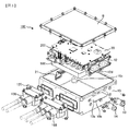
- FIG. 3 is an exploded perspective view of the power conversion apparatus 100 as an embodiment according to the present invention.
- the power conversion device 100 includes a housing 10 and a cover 8 for fixing and protecting the power conversion module 200 with a power conversion module 200 described later as a core, and connection with an external device is performed by connecting a DC power supply input unit and an AC power supply.
- a connector module 120 that is an output section of the control unit, a signal connector 21 that transmits a signal to the control circuit, and an inlet pipe 13 and an outlet pipe 14 for introducing and discharging the cooling medium to and from the flow path forming body 12.
- the flow path forming body 12 and the housing 10 are separate parts as illustrated.
- the power converter 100 Since the power converter 100 has a substantially rectangular shape at the bottom and top surfaces, it can be easily attached to the vehicle and can be easily produced.
- the direction from the bottom surface of the housing 10 to the cover 8 is upward, the opposite is downward, and the vertical direction is the height direction.
- the flow path forming body 12 holds components such as a power semiconductor module 300, a smoothing capacitor module 500, a first AC bus bar 801, and the circuit board 20 described later, and cools them with a cooling medium.
- the housing 10 houses circuit components constituting the power conversion module 200, and an opening is provided in the side wall of the housing 10, and the signal connector 21 is fixed.
- the signal connector 21 is connected to an external control device through the opening, and signal transmission is performed between the control circuit 172 provided on the circuit board 20 and an external control device such as a host control device.
- Low voltage DC power for operating the control circuit in the power converter 100 is supplied from the signal connector 21.
- a connector module 120 for connecting an external device and a direct current and an alternating current power source is fixed to another opening provided on the side wall of the housing 10.
- the connector module 120 is provided with a DC connector portion 138 for transmitting and receiving DC power to and from the battery 136, and a negative power line 139 b and a positive electrode for supplying high voltage DC power to the power converter 100.
- the side power line 139a electrically connects the battery 136 and the smoothing capacitor module 500 or the like.
- the connector module 120 is provided with an AC connector portion 188 for transmitting and receiving an AC current between the motor generator and the power semiconductor module 300, and an AC wiring 189a for supplying high voltage AC power to the motor generator.
- ⁇ 189c electrically connect the motor generator and the power semiconductor modules 300a to 300c.
- FIG. 4 is an exploded perspective view for assisting understanding of the components and the water channel configuration incorporated in the flow path forming body 12 which is a component of the power conversion module 200.
- the flow path forming body 12 has a smaller size in the vertical direction than the dimensions in the other directions and has a flat shape, and an outlet connecting the inlet pipe connection portion 12a and the outlet pipe 14 on the side surface.
- a pipe connecting portion 12b is provided, and the cooling flow path 19 is formed in a U shape so as to connect two pipes.
- the upper surface on one side of the cooling flow path 19 is open.
- the cooling medium flows from the inlet pipe 13, and the flow path 19a into which the power semiconductor module 300a is inserted, the flow path 19b into which the power semiconductor module 300b is inserted, the folded flow path portion 19c, and the flow path into which the power semiconductor module 300c is inserted. It is discharged from the outlet pipe 14 through 19d and the flow path 19e.
- the opening surface 400 is closed by the flow path cover 420 and the flow path cover seal member 405. Further, openings 402a to 402c are formed on the side surface of the flow path forming body 12 along the flow of the refrigerant.
- the openings 402a to 402c are closed by the inserted power semiconductor modules 300a to 300c and the flange seal members 406a to 406c, and the power semiconductor modules 300a to 300c are cooled by the cooling medium flowing through the cooling flow path 19. That is, the power semiconductor modules 300a to 300c are inserted into the cooling channel 19 through the openings 402a to 402c in a direction perpendicular to the flow direction of the cooling medium flowing through the cooling channel 19.
- the power radiating surface 307A and the second radiating surface 307B, which will be described later, in the power semiconductor modules 300a to 300c are parallel to the upper surface and the lower surface of the flow path forming body 12, respectively.
- the semiconductor modules 300a to 300c are cooled.
- the minimum dimension in the height direction of the flow path forming body 12 that houses the power semiconductor module 300 (the minimum distance between the top surface and the bottom surface of the flow path forming body 12) is the power semiconductor module 300. Therefore, the height of the flange 304B, which will be described later, can be reduced to a height obtained by adding the plate thickness of the flow path cover 420 to the width.
- the folded flow path portion 19c is provided in the flow path, and the flexibility of layout of the power semiconductor modules 300a to 300c is increased without deteriorating the cooling performance. Miniaturization is also possible.
- the power semiconductor modules 300a and 300b are provided in the cooling flow path 19 in the refrigerant flow direction 418a, which is the forward path
- the power semiconductor module 300c is provided in the cooling flow path 19 in the refrigerant flow direction 418c, which is the return path. .
- the cooling channel 19 has an effect of increasing the mechanical strength in addition to the cooling effect by making the main structure of the cooling channel 19 of the channel forming body 12 integrally with the channel forming body 12 by casting aluminum. . Moreover, the flow path forming body 12 and the cooling flow path 19 are integrated with each other by being made by aluminum casting, heat conduction is improved, and cooling efficiency is improved.
- the power semiconductor modules 300a to 300c are fixed to the cooling channel 19 to complete the cooling channel 19, and a water leak test is performed on the water channel.
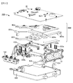
- FIG. 5 is an exploded perspective view for helping understanding the configuration of the power conversion module 200.
- a power semiconductor module 300 is accommodated in the flow path forming body 12.
- the smoothing capacitor module 500 is assembled at a position close to the lower surface of the flow path forming body 12.
- the flow path 19e portion can suppress the depth of the flow path.
- the lower surface has a recessed shape, and a resistor 450 is fixed to the recessed portion.
- a current sensor 180 is fixed with a boss, and a bus bar assembly 800 is also fixed.
- the bus bar assembly 800 includes bus bar bodies 801a, 801b and 801c that transmit AC power, a heat transfer member 803, and a bus bar holding member 802.
- the bus bar assembly 800 is fixed to the flow path cover 420 at the lower part, and the circuit at the upper part. It is fixed to the substrate 20.
- the terminals provided on the smoothing capacitor module 500 and the AC bus bars 801a to 800c are electrically connected to the power semiconductor modules 300a to 300c, and the connecting portions are joined by welding.
- the heat generating components can be arranged close to both the upper surface and the lower surface, that is, the surface having a large area. In contrast, the cooling efficiency is greatly improved.
- the area that can be used for the layout of the smoothing capacitor module 500 can be the same area as that of the flow path forming body 12, the dimension in the height direction is suppressed while ensuring the capacitor capacity necessary for ensuring the inverter performance. Can be reduced in height.
- the board of the driver circuit 174 and the board of the control circuit 172 cannot be arranged on the same plane.
- the driver circuit 174 and the control circuit 172 can be arranged on the same circuit board 20 and the height can be reduced.
- the assembly work including welding is performed by the power conversion module 200. This is possible from all directions, and as a result, the degree of freedom in design is increased, so that it is possible to reduce the size and cost, and the productivity is improved in the production department.
- the inspection can be performed in the state of the power conversion module 200 at the production site.
- the parts such as the housing 10 are not discarded, the yield can be reduced.
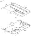
- FIG. 6 illustrates a means for fixing the flow path forming body 12 to the housing 10.
- FIG. 6A is a cross-sectional view of the vicinity of the inlet pipe 13 and the outlet pipe 14.
- FIG. 6B is a cross-sectional view of the facing side of the surface to which the inlet / outlet pipe is attached.
- the flow path forming body 12 is provided with an inlet pipe connecting portion 12a and an outlet pipe connecting portion 12b shown in FIG. 4, and a flange 12c including both the connecting portions is formed.
- the inlet pipe connection part 12a and the outlet pipe connection part 12b connect the cooling flow path 19 of the flow path forming body 12 and an external device.
- the housing 10 is provided with an opening 10a matched to the flow path forming body flange 12c.
- the flange 12 c including the inlet pipe connecting portion 12 a and the outlet pipe connecting portion 12 b is exposed to the outside of the housing 10 through the opening 10 a formed in the housing 10.
- the cooling medium enters the flow path forming body 12 directly from the inlet pipe 13, passes through the cooling flow path 19, and is discharged from the direct outlet pipe 14.
- the required specification for the housing 10 is lower than that of the conventional housing.
- the housing is machined or impregnated in order to prevent leakage of the cooling medium.
- an alternative material such as resin can be selected for the housing 10, it is possible to reduce the weight and reduce the cost.
- An internal thread is provided on the flange 12c provided on the flow path forming body 12 described above, and after the seal member 407 matched to the flange shape is assembled, the fastening screw 31 is used to make a perpendicular to the flange 12c. It is fixed to the housing 10 by tightening from the direction.
- the housing 10 is provided with a female screw 10c on the opposite side of the surface to which the inlet / outlet pipe is attached, and the flange 12e of the flow path forming body 12 is fastened in the vertical direction using the fastening screw 32. .
- a support portion 12d is provided at the lower portion of the flange 12c, and a support portion 10b is provided on the opposite housing 10 so that the load in the vertical direction is received by the indication portion 12d and the support portion 10, and a fastening screw 31 has the function of suppressing the stress in the shearing direction generated at 31.
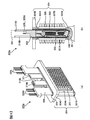
- FIG. 7 describes the flow path cover 420 to help understanding.
- FIG. 7A is a perspective view of the flow path cover 420 as viewed from the side in contact with the opening surface 400 of the flow path forming body 12.
- the flow path cover 420 is provided with a convex portion 420a in accordance with the cooling flow path 19 and the power semiconductor module 300, so that the clearance with the heat radiating portion provided in the power semiconductor module 300 can be made uniform and appropriate. Will improve.
- FIG. 7B is a perspective view of the flow path cover 420 as viewed from the upper surface of the flow path forming body 12.
- the flow path cover 420 has a shape 420b that is recessed according to the convex portion 420a, and an AC bus bar holding member mounting boss 420c is provided in the recessed portion. Since the mounting boss 420c is provided in the recessed portion, the height of the boss can be suppressed and the height can be reduced.
- a circuit board mounting boss 420d is provided on the surface of the flow path cover 420 shown in FIG. Since the mounting boss 420d can be arranged at an arbitrary position, the distance between the support points when mechanical vibration occurs can be shortened, and the resonance frequency can be increased, thereby improving the reliability. In addition, since the flow path cover 420 is located between the power semiconductor module 300 and the circuit board 20, an electromagnetic shielding effect can be obtained. In the conventional configuration, a dedicated metal plate is used, but in the present embodiment, since it can be integrated into the flow path cover 420, there is an effect of cost reduction. If the effect of electromagnetic shielding / board cooling is low, electromagnetic shielding / board cooling can be achieved by placing a thin conductive metal plate between the bus bar assembly 800 and the circuit board 20. However, the effect of cost reduction can be obtained.
- the power semiconductor modules 300a to 300c have the same structure, and the structure of the power semiconductor module 300a will be described as a representative. 7 to 11, the signal terminal 325U corresponds to the gate electrode 154 and the signal emitter electrode 155 disclosed in FIG. 2, and the signal terminal 325L corresponds to the gate electrode 164 and the emitter electrode 165 disclosed in FIG. To do.
- the DC positive terminal 315B is the same as the positive terminal 157 disclosed in FIG. 2, and the DC negative terminal 319B is the same as the negative terminal 158 disclosed in FIG.
- the AC terminal 321 is the same as the AC terminal 159 disclosed in FIG.
- FIG. 8A is a perspective view in which the terminal shape is changed so that the power semiconductor module 300a of the present embodiment can be easily explained.
- FIG. 8B is a cross-sectional view of the power semiconductor module 300a of this embodiment.
- the power semiconductor elements (IGBT 328, IGBT 330, diode 156, and diode 166) constituting the series circuit 150 of the upper and lower arms are connected by the conductor plate 315 or the conductor plate 318 or the conductor plate 316 or the conductor plate as shown in FIGS. By 319, it is fixed by being sandwiched from both sides.
- These conductor plates are assembled with an auxiliary molded body 600 formed by integrally molding the signal wirings which are the signal terminals 325U and 325L.
- the conductor plate 315 and the like are sealed with the first sealing resin 348 with the heat dissipation surface exposed, and the insulating sheet 333 is thermocompression bonded to the heat dissipation surface.
- the module primary sealing body 302 sealed with the first sealing resin 348 is inserted into the module case 304 and sandwiched with the insulating sheet 333, and is thermocompression bonded to the inner surface of the module case 304 that is a CAN type cooler.
- the CAN-type cooler is a cylindrical cooler having an insertion port 306 on one surface and a bottom on the other surface.
- the module case 304 is made of an aluminum alloy material such as Al, AlSi, AlSiC, Al—C, etc., and is formed by joining one or a plurality of parts.
- the module case 304 has a structure in which no opening other than the insertion port 306 is provided.
- the insertion port 306 is surrounded by a flange 304B.
- the first heat radiating surface 307A and the second heat radiating surface 307B which are wider than the other surfaces, are arranged facing each other, and the facing first heat radiating surface 307A and The three surfaces connected to the second heat radiating surface 307B constitute a surface sealed with a narrower width than the first heat radiating surface 307A and the second heat radiating surface 307B, and the insertion port 306 is formed on the other side surface.
- the shape of the module case 304 does not have to be an accurate rectangular parallelepiped, and the corners may form a curved surface as shown in FIG.
- the metallic case having such a shape By using the metallic case having such a shape, even when the module case 304 is inserted into the cooling channel 19 through which a coolant such as water or oil flows, a seal against the coolant can be secured by the flange 304B. It is possible to prevent the medium from entering the inside of the module case 304 with a simple configuration. Further, the fins 305 are uniformly formed on the first heat radiation surface 307A and the second heat radiation surface 307B facing each other.
- a curved portion 304A having an extremely thin thickness is formed on the outer periphery of the first heat radiating surface 307A and the second heat radiating surface 307B. Since the curved portion 304A is extremely thin to such an extent that it can be easily deformed by pressurizing the fin 305, the productivity after the module primary sealing body 302 is inserted is improved.
- the gap remaining inside the module case 304 is filled with the second sealing resin 351. Further, as shown in FIGS. 9 and 10, a DC positive electrode wiring 315A and a DC negative electrode wiring 319A for electrical connection with the smoothing capacitor module 500 are provided, and a DC positive electrode terminal 315B (157) is provided at the tip thereof. ) And a DC negative terminal 319B (158). An AC wiring 320 for supplying AC power to the motor generator or 194 is provided, and an AC terminal 321 (159) is formed at the tip thereof.
- the DC positive electrode wiring 315A is integrally formed with the conductor plate 315
- the DC negative electrode wiring 319A is integrally formed with the conductor plate 319
- the AC wiring 320 is integrally formed with the conductor plate 316.
- the gap between the conductor plate and the inner wall of the module case 304 can be reduced, and the power semiconductor element The generated heat can be efficiently transmitted to the fins 305.
- the generation of thermal stress can be absorbed by the insulating sheet 333, which is favorable for use in a power conversion device for a vehicle having a large temperature change. .
- FIG. 9A is an internal cross-sectional view in which the module case 304, the insulating sheet 333, the first sealing resin 348, and the second sealing resin 351 are removed in order to help understanding.
- FIG. 9B is an internal perspective view.
- FIG. 10 (a) is an exploded view for helping understanding of the structure of FIG. 9 (b).
- FIG. 10B is a circuit diagram of the power semiconductor module 300.
- FIG. 11A is a circuit diagram for explaining the inductance reduction effect
- FIG. 11B is a perspective view showing a current flow for explaining the inductance reduction effect.
- the direct current positive electrode side conductor plate 315 and the alternating current output side conductor plate 316 are arranged in substantially the same plane.
- the collector electrode of the IGBT 328 on the upper arm side and the cathode electrode of the diode 156 on the upper arm side are fixed.
- the collector electrode of the IGBT 330 on the lower arm side and the cathode electrode of the diode 166 on the lower arm side are fixed.
- the AC conductor plate 318 and the conductor plate 319 are arranged in substantially the same plane.
- the emitter electrode of the IGBT 328 on the upper arm side and the anode electrode of the diode 156 on the upper arm side are fixed.
- an emitter electrode of the IGBT 330 on the lower arm side and an anode electrode of the diode 166 on the lower arm side are fixed.
- Each power semiconductor element is fixed to an element fixing portion 322 provided on each conductor plate via a metal bonding material 160.
- the metal bonding material 160 is, for example, a low-temperature sintered bonding material including a solder material, a silver sheet, and fine metal particles.
- Each power semiconductor element has a flat plate-like structure, and each electrode of the power semiconductor element is formed on the front and back surfaces. As shown in FIG. 9A, each electrode of the power semiconductor element is sandwiched between the conductor plate 315 and the conductor plate 318, or the conductor plate 316 and the conductor plate 319. In other words, the conductor plate 315 and the conductor plate 318 are stacked so as to face each other substantially in parallel via the IGBT 328 and the diode 156. Similarly, the conductor plate 316 and the conductor plate 319 have a stacked arrangement facing each other substantially in parallel via the IGBT 330 and the diode 166. Further, the conductor plate 316 and the conductor plate 318 are connected via an intermediate electrode 329. By this connection, the upper arm circuit and the lower arm circuit are electrically connected to form an upper and lower arm series circuit.
- the direct current positive electrode wiring 315A and the direct current negative electrode wiring 319A have a shape extending substantially in parallel while facing each other through an auxiliary mold body 600 formed of a resin material.
- the signal terminal 325U and the signal terminal 325L are formed integrally with the auxiliary mold body 600 and extend in the same direction as the DC positive electrode wiring 315A and the DC negative electrode wiring 319A.
- a thermosetting resin having an insulating property or a thermoplastic resin is suitable.
- the direct current positive electrode wiring 315A and the direct current negative electrode wiring 319A are arranged so as to face each other substantially in parallel, so that currents that instantaneously flow during the switching operation of the power semiconductor element face each other in the opposite direction. As a result, the magnetic fields produced by the currents cancel each other out, and this action can reduce the inductance.
- the lower arm side diode 166 is in a conductive state in a forward bias state. In this state, when the upper arm side IGBT 328 is turned on, the diode 166 on the lower arm side is reversely biased, and a recovery current caused by carrier movement passes through the upper and lower arms.
- a recovery current 360 shown in FIG. 11B flows through each of the conductor plates 315, 316, 318, and 319. As indicated by the dotted line, the recovery current 360 passes through the DC positive terminal 315B (157) disposed opposite to the DC negative terminal 319B (158), and is subsequently formed by the conductor plates 315, 316, 318, and 319. It flows through the loop-shaped path, and again flows as shown by the solid line through the DC negative terminal 319B (158) arranged opposite to the DC positive terminal 315B (157).
- the eddy current 361 flows through the first heat radiating surface 307A and the second heat radiating surface 307B of the module case 304 by the current flowing through the loop-shaped path. Due to the magnetic field canceling effect generated by the equivalent circuit 362 in the current path of the eddy current 361, the wiring inductance 363 in the loop-shaped path is reduced.
- the loop-shaped current path flows through a path close to the DC positive terminal 315B (157) side of the conductor plate 315 and passes through the IGBT 328 and the diode 156 as indicated by a dotted line.
- the loop-shaped current path flows through a path farther from the DC positive terminal 315B (157) side of the conductor plate 318 as shown by the solid line, and then farther from the DC positive terminal 315B (157) side of the conductor board 316 as shown by the dotted line.
- the path flows through the IGBT 330 and the diode 166.
- the loop-shaped current path flows along a path close to the DC negative electrode wiring 319A side of the conductor plate 319.
- the loop-shaped current path passes through a path closer to or farther from the DC positive terminal 315B (157) or the DC negative terminal 319B (158), thereby forming a current path closer to the loop shape. Is done.
- FIG. 12 (a) is a perspective view of the auxiliary mold body 600
- FIG. 12 (b) is a transparent view of the auxiliary mold body 600.
- the auxiliary mold body 600 has the signal conductor 324 integrated by insert molding.
- the signal conductor 324 receives the temperature information of the upper arm side gate electrode terminal 154 and the emitter electrode terminal 155, the upper arm side gate electrode terminal 164 and the emitter electrode terminal 165 (see FIG. 2), and the power semiconductor element.
- a terminal for transmission is included. In the description of this embodiment, these terminals are collectively referred to as signal terminals 325U and 325L.
- the signal conductor 324 forms signal terminals 325U and 325L at one end, and forms element-side signal terminals 326U and 326L at the other end.
- the element-side signal terminals 326U and 326L are connected to signal pads provided on the surface electrode of the power semiconductor element by, for example, wires.
- the first sealing portion 601A has a shape extending in a direction transverse to the major axis of the shape of the DC positive electrode wiring 315A, the DC negative electrode wiring 319A, or the AC wiring 320 shown in FIG.
- the second sealing portion 601B has a shape extending in a direction substantially parallel to the major axis of the shape of the DC positive electrode wiring 315A, the DC negative electrode wiring 319A, or the AC wiring 320.
- the second sealing portion 601B includes a sealing portion for sealing the signal terminal 325U on the upper arm side and a sealing portion for sealing the signal terminal 325L on the lower arm side.
- the auxiliary mold body 600 is formed so that its length is longer than the entire length of the conductor plates 315 and 316 arranged side by side or the entire length of the conductor plates 319 and 320 arranged side by side. That is, the lengths of the conductor plates 315 and 316 arranged side by side or the lengths of the conductor plates 319 and 320 arranged side by side are within the range of the lateral length of the auxiliary mold body 600.
- the first sealing portion 601A has a hollow shape and forms a wiring fitting portion 602B for fitting the DC negative electrode wiring 319A into the hollow.
- the first sealing portion 601A has a hollow shape and forms a wiring fitting portion 602A for fitting the DC positive electrode wiring 315A into the hollow.
- the first sealing portion 601A is disposed on the side of the wiring fitting portion 602A, has a hollow shape, and further forms a wiring fitting portion 602C for fitting the AC wiring 320 into the hollow. To do.
- Each wiring is positioned by fitting each wiring to these wiring fitting portions 602A to 602C. Thereby, it becomes possible to perform the filling operation of the resin sealing material after firmly fixing each wiring, and the mass productivity is improved.
- the wiring insulation part 608 protrudes in a direction away from the first sealing part 601A from between the wiring fitting part 602A and the wiring fitting part 602B. Since the plate-shaped wiring insulating portion 608 is interposed between the DC positive electrode wiring 315A and the DC negative electrode wiring 319A, it is possible to arrange the wiring insulating portion 608 so as to reduce the inductance while ensuring insulation.
- the first sealing portion 601A is formed with a mold pressing surface 604 that comes into contact with a mold used for resin sealing, and the mold pressing surface 604 prevents resin leakage during resin sealing.
- a protruding portion 605 for preventing is formed around the outer periphery in the longitudinal direction of the first sealing portion 601.
- a plurality of protrusions 605 are provided to enhance the resin leakage prevention effect.
- the protrusions 605 are also provided in the wiring fitting part 602A and the wiring fitting part 602B, it is possible to prevent the resin sealing material from leaking from the periphery of the DC positive electrode wiring 315A and the DC negative electrode wiring 319A.
- the material of the first sealing portion 601A, the second sealing portion 601B, and the protrusion 605 is a heat that can be expected to have high heat resistance in consideration of being installed in a mold of about 150 to 180 ° C.
- a liquid crystal polymer of plastic resin, polybutylene terephthalate (PBT) or polyphenylene sulfide resin (PPS) is desirable.
- a plurality of through holes 606 shown in FIG. 12B are provided in the longitudinal direction on the power semiconductor element side in the short direction of the first sealing portion 601A.
- the first sealing resin 348 flows into the through-hole 606 and hardens, whereby an anchor effect is exerted, and the auxiliary mold body 600 is firmly held by the first sealing resin 348, and temperature changes and machine Even if stress is applied by mechanical vibration, both do not peel off. It is difficult to peel even if the shape is uneven instead of the through hole.
- a certain degree of effect can be obtained by applying a polyimide coating agent to the first sealing portion 601A or roughening the surface.
- the auxiliary mold body 600 supporting each wiring is inserted into a mold preheated to about 150 to 180 ° C.
- the auxiliary mold body 600, the direct current positive electrode wiring 315A, the direct current negative electrode wiring 319A, the alternating current wiring 320, the conductor plate 315, the conductor plate 316, the conductor plate 318, and the conductor plate 319 are firmly connected to each other.
- the second sealing portion 601B is formed to extend from the vicinity of the module case 304 to the vicinity of the driver circuit board.
- the switching control signal can be normally transmitted even when exposed to a high voltage.
- the DC positive wiring 315A, the DC negative wiring 319A, the AC wiring 320, the signal terminal 325U, and the signal terminal 325L protrude from the module case 304 in the same direction, it is possible to ensure electrical insulation and ensure reliability. it can.
- FIG. 13 is an exploded perspective view for explaining the internal structure of the smoothing capacitor module 500.
- the laminated conductor plate 501 is composed of a negative electrode conductor plate 505 and a positive electrode conductor plate 507 formed of plate-like wide conductors, and an insulating sheet (not shown) sandwiched between the negative electrode conductor plate 505 and the positive electrode conductor plate 507. .
- the laminated conductor plate 501 cancels out the magnetic flux with respect to the current flowing through the series circuit 150 of the upper and lower arms of each phase, so that the inductance of the current flowing through the series circuit 150 of the upper and lower arms is reduced.
- the laminated conductor plate 501 has a substantially square shape.
- the negative power supply terminal 508 and the positive power supply terminal 509 are formed so as to rise from one side of the laminated conductor plate 501 and are connected to the positive conductor plate 507 and the negative conductor plate 505, respectively.
- DC power is supplied to the positive power supply terminal 509 and the negative power supply terminal 508 via the DC connector 138 as described with reference to FIG.
- the capacitor terminal 503c is raised from the same side as the negative power supply terminal 508 and the positive power supply terminal 509, and the capacitor terminals 503a and 503b are raised from opposite sides of the capacitor terminal 503c. It is formed corresponding to the positive terminal 157 (315B) and the negative terminal 158 (319B) of the semiconductor module 300. Capacitor terminals 503a to 503c are connected to power semiconductor modules 300a to 300c, respectively. A part of an insulating sheet (not shown) is provided between the negative-side capacitor terminal 504a and the positive-side capacitor terminal 506a constituting the capacitor terminal 503a to ensure insulation. The same applies to the other capacitor terminals 503b and 503c.
- the negative electrode conductor plate 505, the positive electrode conductor plate 507, the battery negative electrode side terminal 508, the battery negative electrode side terminal 509, and the capacitor terminals 503a to 503f are composed of integrally formed metal plates, and the upper and lower arms This has the effect of reducing the inductance with respect to the current flowing through the series circuit 150.
- a plurality of capacitor cells 514 are provided on the inner side of the smoothing capacitor module 500 below the laminated conductor plate 501.
- four capacitor cells 514 are arranged in a line along one side of multilayer conductor plate 501, and another twelve capacitor cells 514 are along the other side of multilayer conductor plate 501.
- a total of 16 capacitor cells are provided.
- the refrigerant flow path is provided in the state close to the upper surface of the smoothing capacitor module 500, and the cooling efficiency is improved.
- Capacitor cell 514 is a unit structure of a power storage unit of smoothing capacitor module 500, and two films each having a metal such as aluminum deposited thereon are stacked and wound to form a positive electrode and a negative electrode, respectively. Use a film capacitor.
- the electrode of the capacitor cell 514 is manufactured by spraying a conductor such as tin, with the wound shaft surfaces serving as a positive electrode and a negative electrode, respectively.
- the capacitor case 502 includes a storage portion 511 for storing the capacitor cell 514, and the storage portion 511 has a substantially rectangular upper surface and lower surface shown in the drawing.
- the capacitor case 502 is provided with fixing means for fixing the smoothing capacitor module 500 to the flow path forming body 12, for example, holes 520a to 520d for allowing screws to pass therethrough.
- the bottom surface portion 513 of the storage portion 511 has a smooth uneven shape or corrugated shape so as to match the surface shape of the cylindrical capacitor cell 514. This facilitates positioning of the module in which the laminated conductor plate 501 and the capacitor cell 514 are connected to the capacitor case 502.
- the capacitor case 502 is filled with a filler (not shown). Since the bottom surface portion 513 has a corrugated shape in accordance with the shape of the capacitor cell 514, the capacitor cell 514 can be prevented from being displaced from a predetermined position when the filler is filled in the capacitor case 502.
- the capacitor cell 514 generates heat due to a ripple current at the time of switching due to the electric resistance of the metal thin film and the internal conductor deposited on the internal film. Therefore, in order to easily release the heat of the capacitor cell 514 through the capacitor case 502, the capacitor cell 514 is molded with a filler. Furthermore, the moisture resistance of the capacitor cell 514 can be improved by using a resin filler.
- the tip of the AC terminal 321 (159) of the power semiconductor module 300 is connected to the tips of the AC bus bars 801a to 801c by welding.
- the bus bar assembly 800 includes AC bus bars 801a to 801c, a heat transfer member 803, and a bus bar holding member 802.
- the AC bus bars 801a to 801c and the heat transfer member 803 are fixed to the flow path cover 420 by the bus bar holding member 802. Since heat generated by energization of the AC bus bars 801a to 801c is transmitted to the flow path forming body 12 via the heat transfer member 803, there is an effect of cooling the AC bus bars 801a to 801c.
- FIG. 14 is a perspective view disassembled into components for explaining the overall configuration of the connector module 120.
- DC bus bars 814 a and 814 b are held by a DC bus bar holding member 818 and fixed to the connector housing 121. One ends of the DC bus bars 814 a and 814 b are respectively connected to the positive power terminal 509 and the negative power terminal 508 provided in the smoothing capacitor module 500.
- the second AC bus bars 804 a to 804 c are held by an AC bus bar holding member 817 and fixed to the connector housing 121. One ends of the second AC bus bars 804a to 804c are connected to the first AC bus bars 801a to 801c included in the power conversion module 200, respectively.
- the other ends of the DC bus bars 814a and 814b and the second AC bus bars 804a to 804c are generally connected to a DC wiring 139 and an AC wiring 189 provided on the vehicle side.
- the DC bus bar 814 and the DC wiring 139 are fastened with the fastening screw 36 shown in FIG. 15 and sealed with the DC connector cover 822.
- the AC wiring 189 is inserted into the AC connector portion 188 of the connector housing 121
- the second AC bus bar 804 and the AC wiring 189 are fastened with the fastening screw 35 shown in FIG. 15 and sealed with the AC connector cover 821. It is configured to do.
- the connector module 120 has the DC connector portion 138 and the AC connector portion 188 integrated, but each connector module 120 may be separately manufactured and fixed to the housing 10.
- the connection between the DC wiring 139 and the AC wiring 189 is fastened with a screw.
- the above-described effect can be obtained in the same manner by using a metal spring force to ensure electrical contact.
- FIG. 15 is a view from the top surface of the power converter 100 with the cover 8 removed.
- FIG. 16 is a perspective view showing parts easily attached to the side surface of the power conversion apparatus 100 shown in FIG.
- the components are assembled in a module state, and are fixed to the housing 10 with fastening screws 31 and 32.
- the fastening screw 32 performs a fastening operation from the opening of the housing 10, and the fastening screw 31 performs a fastening operation from the external side surface.
- the fixing position of the housing 10 to the vehicle can be freely set. It is possible to obtain effects such as cost reduction of molds when manufacturing, standardization of production equipment, and reduction of design man-hours.
- the inlet pipe 13, the outlet pipe 14, the connector module 120, and the signal connector 21 are fastened with fastening screws 33, 34, and 37, and the DC bus bar 814 and the power terminals 508 and 509 are fastened with the fastening screws 36.
- the 1 AC bus bar 801 and the second AC bus bar 804 are connected by the fastening screw 35.
- the board connector 38 of the signal connector 21 into the circuit board 20, the connection of each part is completed.
- only the cooling medium connection pipes 13 and 14, the signal connector 21, the DC connector part 138, and the AC connector part 188 that are interfaces with external devices are changed. Since a wide range of measures can be taken, effects such as standardization of parts, cost reduction of molds of component parts, standardization of production facilities, reduction of design man-hours, and the like can be obtained.
- FIG. 17 is a cross-sectional view of the flow path forming body and the cooling medium passage of the power semiconductor module 300.
- FIG. 17A is a cross-sectional view of a conventional configuration
- FIG. 17B is a cross-sectional view of the present embodiment.
- the flow path forming body generally uses die-cast aluminum in consideration of strength, heat dissipation, sealing performance of the cooling refrigerant, cost, and the like. Die casting is a manufacturing method in which molten aluminum is injected into a metal mold at a high pressure, and the product is taken out of the mold after cooling. Therefore, the surface parallel to the mold drawing direction is tapered so that the mold and the product can be easily separated when the product is taken out.
- the power semiconductor module 300 is inserted from the upper surface of the flow path forming body 901, and the lower surface of the flow forming body 901 is sealed by the lower cover 902. Yes.
- the die is drawn in the direction of the upper die casting die 912 and the lower die casting die 913 with the die dividing surface 911 as a boundary.
- a tapered surface 914 is required.
- the clearance 916 between the heat radiation fin 305 and the tapered surface 914 provided in the power semiconductor module 300 differs depending on the location.
- the cooling refrigerant passes through a large portion, the cooling performance is non-uniform, and there is a concern that the performance of the power semiconductor module 300 may be reduced.
- the taper surface 914 can be machined to make the clearance 916 uniform. However, since machining is required, this has been a factor in increasing costs.
- the power semiconductor module 300 is inserted from the side surface of the flow path forming body 12, and the upper surface of the flow path forming body 12 is sealed with the flow path cover 420. It is configured to be stopped.
- the die is drawn in the upward die casting direction 922.
- the tapered surface 924 which is a surface parallel to the drawing direction is close to the side surface of the power semiconductor module 300 which is a surface perpendicular to the heat radiation fin 305 of the power semiconductor module 300.
- the surface close to the heat radiation fin 305 provided in the power semiconductor module 300 becomes a surface 925 that does not require a taper, so that a uniform and minimum clearance 926 can be secured. This can improve the performance of the power semiconductor module 300 and can reduce the cost because machining is unnecessary.
- the power conversion device described in the above-described embodiment and the system using this device solve various problems that are desired to be solved for commercialization.
- One of the various problems solved by these embodiments is an improvement in productivity.
- the above problem can be solved not only by the configuration described above but also by other configurations.
- a power semiconductor module is inserted from the side of the refrigerant passage, a smoothing capacitor module is arranged on the lower surface of the refrigerant passage, an AC bus bar and a circuit board are arranged on the upper surface of the refrigerant passage. It has a configuration in which it is modularized, the module is assembled to a housing, and electrical wiring, refrigerant piping, and signal wiring are assembled.
- the entire configuration of the power conversion device can be arranged in a more orderly manner, and the power conversion device can be reduced in size. Further, it is possible to obtain a low profile effect that can further reduce the size of the power converter in the lateral direction across the refrigerant flow path.
- a flow path forming body that forms a refrigerant flow path is provided along the upper surface of the smoothing capacitor module, and the smoothing capacitor module is fixed to the flow path forming body so that the power flow is increased by the refrigerant flow path.
- the semiconductor module and the smoothing capacitor module can be cooled together. Further, since the AC bus bar and the circuit board can be arranged close to the refrigerant passage side, cooling can be performed efficiently.
Abstract
In the present invention, a power convertor includes the following: a power semiconductor module; a smoothing capacitor module; an AC bus bar; a control circuit for controlling a power semiconductor element; and a flow path forming body which forms a flow path in which a coolant flows. The power semiconductor module has a first heat radiation part and a second heat radiation part facing the first heat radiation part. The flow path forming body outer form part of the flow path forming body has a first surface wall facing the first heat radiation part with the flow path interposed therebetween, a second surface wall facing the second radiation part with the flow path interposed therebetween, and a lateral wall which connects the first surface wall and the second surface wall. The lateral wall has an opening for the insertion of the power semiconductor module into the flow path.
Description
本発明は直流電力を交流電力に変換しあるいは交流電力を直流電力に変換するために使用する電力変換装置に関する。
The present invention relates to a power converter used for converting DC power into AC power or converting AC power into DC power.
電力変換装置の一例は日本国特開2008-193867号公報に開示されている。
An example of a power converter is disclosed in Japanese Patent Application Laid-Open No. 2008-193867.
日本国特開2008-193867号公報においては、半導体モジュールは両側に冷却金属を有し冷却金属の間に上アーム用の半導体チップと下アーム用の半導体チップとを挟み込み、半導体モジュールを水路筐体本体部に挿入される構成が開示されている。
In Japanese Patent Application Laid-Open No. 2008-193867, the semiconductor module has a cooling metal on both sides, and the semiconductor chip for the upper arm and the semiconductor chip for the lower arm are sandwiched between the cooling metals, and the semiconductor module is placed in the water channel housing. The structure inserted in a main-body part is disclosed.
しかしながら、日本国特開2008-193867号公報に記載の発明によると、インバータ全体寸法が(特に高さ方向)が大型化してしまうという問題があった。
However, according to the invention described in Japanese Patent Application Laid-Open No. 2008-193867, there is a problem that the overall dimensions of the inverter (particularly in the height direction) are increased.
本発明の第1の態様によると、電力変換装置は、直流電流を交流電流に変換するパワー半導体素子を有するパワー半導体モジュールと、前記直流電流を平滑化する平滑コンデンサモジュールと、前記パワー半導体素子の交流電流出力を伝達するための交流バスバーと、前記パワー半導体素子を制御する制御回路部と、冷媒を流す流路を形成する流路形成体とを備える。前記パワー半導体モジュールは、第1放熱部と、前記パワー半導体素子を介して第1放熱部と対向する第2放熱部と、を有し、前記流路形成体の流路形成体外形部は、前記パワー半導体モジュールの前記第1放熱部に前記流路を介して対向する第1面壁と、前記パワー半導体モジュールを挟んで前記第1面壁の反対側で前記パワー半導体モジュールの前記第2放熱部に前記流路を介して対向する第2面壁と、前記第1面壁と前記第2面壁とを繋ぐ側壁と、を有し、前記側壁は、前記パワー半導体モジュールを前記流路内に挿入するための開口を有し、前記平滑コンデンサモジュールは、前記流路形成体外形部の前記第2面壁に向き合う位置に配置され、前記交流バスバーは、前記流路形成体外形部の前記第1面壁に向き合う位置に配置され、前記制御回路部は、前記交流バスバーを挟んで前記流路形成体外形部の前記第1面壁の反対側で前記交流バスバーに向き合う位置に配置される。
本発明の第2の態様によると、第1の態様の電力変換装置において、流路形成体は、ハウジングとは物理的に分離して形成されるとともに、固定具によりハウジングに固定されることが好ましい。
本発明の第3の態様によると、第1の態様の電力変換装置において、パワー半導体モジュールと平滑コンデンサモジュールと交流バスバーと制御回路部とが流路形成体に組付けられた状態で、さらにハウジングに組付けられることが好ましい。
本発明の第4の態様によると、第1の態様の電力変換装置において、流路形成体の流路と外部装置との接続部は、ハウジングに形成された開口を通ってハウジングの外部に露出されることが好ましい。
本発明の第5の態様によると、第1の態様の電力変換装置において、流路形成体の流路と外部装置との接続部分を具備するフランジ部をさらに備え、フランジ部は、筐体となるケースと接触する部分にシール部材を含むことが好ましい。
本発明の第6の態様によると、第1の態様の電力変換装置において、流路形成体の第1面壁は開口を有し、流路形成体は、第1面壁が有する開口を塞ぐ流路カバーをさらに含むことが好ましい。
本発明の第7の態様によると、第6の態様の電力変換装置において、流路カバーの流路側の表面の形状は、流路形成体の内部の形状とパワー半導体モジュールの外形とに対応する凸の形状であることが好ましい。
本発明の第8の態様によると、第7の態様の電力変換装置において、流路カバーの流路側とは反対側の表面は、凸形状に合わせて凹ませた部分を含み、流路カバーは、凹ませた部分に交流バスバーを固定するためのボスを有することが好ましい。
本発明の第9の態様によると、第1の態様の電力変換装置において、流路形成体は、電流センサを取り付けるためのボスを有することが好ましい。
本発明の第10の態様によると、第1の態様の電力変換装置において、流路形成体は、回路基板を取り付けるためのボスを有することが好ましい。
本発明の第11の態様によると、第1の態様の電力変換装置において、制御回路部は、ドライバ回路と制御回路とを構成するそれぞれの部品が、一枚の基板上に配置されることによって構成されることが好ましい。
本発明の第12の態様によると、第1の態様の電力変換装置において、流路形成体の第1面壁と第2面壁との間の最小距離は、パワー半導体モジュールのケースに具備されたフランジの寸法と略同一であることが好ましい。
本発明の第13の態様によると、第1の態様の電力変換装置において、流路形成体は所定の物質を型に鋳込む製法で製作され、側壁の表面は傾斜を持ったテーパー面であり、第1面壁および第2面壁の表面はテーパーを必要としない面であることが好ましい。
本発明の第14の態様によると、モータに接続された第1の態様の電力変換装置において、交流バスバーは、交流電流出力をモータへ伝達し、流路形成体の流路は、隔壁を設けることでU字形状に形成され、パワー半導体モジュールは、流路を流れる冷媒の流れ方向に対して垂直の方向に、側壁が有する開口を通じて流路内に挿入されることによって、第1放熱部と第2放熱部とがそれぞれ第1面壁と第2面壁とに対して平行となることが好ましい。 According to the first aspect of the present invention, a power conversion device includes a power semiconductor module having a power semiconductor element that converts a direct current into an alternating current, a smoothing capacitor module that smoothes the direct current, and the power semiconductor element. An AC bus bar for transmitting an AC current output, a control circuit unit for controlling the power semiconductor element, and a flow path forming body for forming a flow path for flowing the refrigerant. The power semiconductor module includes a first heat radiating portion and a second heat radiating portion facing the first heat radiating portion via the power semiconductor element, and the flow path forming body outer shape portion of the flow path forming body includes: A first surface wall facing the first heat radiating portion of the power semiconductor module via the flow path, and a second heat radiating portion of the power semiconductor module on the opposite side of the first surface wall across the power semiconductor module A second wall facing the channel and a side wall connecting the first wall and the second wall, the side wall for inserting the power semiconductor module into the channel. And the smoothing capacitor module is disposed at a position facing the second surface wall of the flow path forming body outer shape portion, and the AC bus bar is positioned at the position facing the first surface wall of the flow path forming body outer shape portion. Placed in Serial control circuit unit is arranged at a position facing to the AC bus bar on the opposite side of the first wall of the flow channel forming extracorporeal form part across the AC bus bar.
According to the second aspect of the present invention, in the power conversion device of the first aspect, the flow path forming body is formed physically separated from the housing, and is fixed to the housing by a fixture. preferable.
According to the third aspect of the present invention, in the power conversion device according to the first aspect, the power semiconductor module, the smoothing capacitor module, the AC bus bar, and the control circuit unit are further assembled to the flow path forming body. It is preferable to be assembled to.
According to the fourth aspect of the present invention, in the power conversion device according to the first aspect, the connection portion between the flow path of the flow path forming body and the external device is exposed to the outside of the housing through the opening formed in the housing. It is preferred that
According to the fifth aspect of the present invention, in the power conversion device of the first aspect, the power conversion device of the first aspect further includes a flange portion including a connection portion between the flow path of the flow path forming body and the external device, It is preferable that a seal member is included in a portion in contact with the case.
According to the sixth aspect of the present invention, in the power conversion device of the first aspect, the first surface wall of the flow path forming body has an opening, and the flow path forming body closes the opening of the first surface wall. It is preferable to further include a cover.
According to the seventh aspect of the present invention, in the power converter of the sixth aspect, the shape of the surface of the flow path cover on the flow path side corresponds to the internal shape of the flow path forming body and the external shape of the power semiconductor module. A convex shape is preferred.
According to the eighth aspect of the present invention, in the power conversion device of the seventh aspect, the surface of the flow path cover on the side opposite to the flow path side includes a recessed portion in conformity with the convex shape. It is preferable to have a boss for fixing the AC bus bar to the recessed portion.
According to the ninth aspect of the present invention, in the power conversion device of the first aspect, it is preferable that the flow path forming body has a boss for attaching the current sensor.
According to the tenth aspect of the present invention, in the power conversion device of the first aspect, it is preferable that the flow path forming body has a boss for attaching the circuit board.
According to the eleventh aspect of the present invention, in the power conversion device according to the first aspect, the control circuit unit is configured such that each component constituting the driver circuit and the control circuit is arranged on one substrate. Preferably, it is configured.
According to the twelfth aspect of the present invention, in the power converter of the first aspect, the minimum distance between the first surface wall and the second surface wall of the flow path forming body is a flange provided in the case of the power semiconductor module. It is preferable that the dimensions are substantially the same.
According to the thirteenth aspect of the present invention, in the power conversion device of the first aspect, the flow path forming body is manufactured by a manufacturing method in which a predetermined substance is cast into a mold, and the surface of the side wall is a tapered surface having an inclination. The surfaces of the first surface wall and the second surface wall are preferably surfaces that do not require a taper.
According to the fourteenth aspect of the present invention, in the power converter of the first aspect connected to the motor, the alternating current bus bar transmits the alternating current output to the motor, and the flow path forming body has the partition wall provided with the partition wall. The power semiconductor module is inserted into the flow path through the opening of the side wall in the direction perpendicular to the flow direction of the refrigerant flowing through the flow path, thereby It is preferable that the second heat radiating portion is parallel to the first surface wall and the second surface wall, respectively.
本発明によれば、電力変換装置の寸法の縮小(低背化)が可能となり、さらに低コストを実現できる。
According to the present invention, it is possible to reduce the size (lower profile) of the power conversion device, and to further reduce the cost.
日本国特開2008-193867号公報に記載の発明によると、半導体モジュールを挿入するための開口は、水路筐体の上面側に設けられている。そのため、半導体のモジュールの高さ方向にある程度スペースを設ける必要が生じ、結果としてインバータ全体寸法が(特に高さ方向)が大型化してしまう。半導体モジュールを挿入するための開口を、水路筐体の側面側に設けることにより、電力変換装置の構成部品の低背化を達成することができ、生産組立性が向上し、低コスト化も達成できると考えられる。本発明の目的は、従来の電力変換装置に対し、寸法の縮小(低背化)・低コスト化が可能な電力変換装置を提供することにある。図面を使用して本発明に係る実施の形態を説明する。
According to the invention described in Japanese Patent Laid-Open No. 2008-193867, the opening for inserting the semiconductor module is provided on the upper surface side of the water channel housing. Therefore, it is necessary to provide some space in the height direction of the semiconductor module, and as a result, the overall dimensions of the inverter (particularly in the height direction) are increased. By providing an opening for inserting a semiconductor module on the side of the water channel housing, it is possible to reduce the height of the components of the power conversion device, improve production assembly, and reduce costs. It is considered possible. An object of the present invention is to provide a power conversion device capable of reducing the size (reducing the height) and reducing the cost of the conventional power conversion device. Embodiments according to the present invention will be described with reference to the drawings.
図1は、本発明に係る電力変換装置を、エンジンとモータの両方を使用して走行するいわゆるハイブリッド用自動車に適用したシステムである。本発明に係る電力変換装置はハイブリッド用車両のみならず、モータのみで走行するいわゆる電気自動車にも適用可能であり、また一般産業機械に使用されているモータを駆動する為の電力変換装置としても使用可能である。
FIG. 1 shows a system in which a power converter according to the present invention is applied to a so-called hybrid vehicle that travels using both an engine and a motor. The power conversion device according to the present invention can be applied not only to a hybrid vehicle but also to a so-called electric vehicle that travels only by a motor, and also as a power conversion device for driving a motor used in a general industrial machine. It can be used.
しかし上述あるいは以下に説明のとおり、本発明に係る電力変換装置は特に上記ハイブリッド用自動車や上記電気自動車に適用すると、小型化の観点あるいは信頼性の観点、その他、いろいろの観点で優れた効果が得られる。ハイブリッド用自動車に適用した電力変換装置は電気自動車に適用した電力変換装置と略同じ構成であり、代表例としてハイブリッド自動車に適用した電力変換装置について説明する。
However, as described above or below, when the power conversion device according to the present invention is applied particularly to the hybrid vehicle or the electric vehicle described above, it has excellent effects from various viewpoints in terms of downsizing or reliability. can get. The power conversion device applied to the hybrid vehicle has substantially the same configuration as the power conversion device applied to the electric vehicle, and the power conversion device applied to the hybrid vehicle will be described as a representative example.
図1は、ハイブリッド自動車(以下「HEV」と記述する)の制御ブロックを示す図である。エンジン(ENG)及びモータジェネレータ(MG)は車両の走行用トルクを発生する。またモータジェネレータは回転トルクを発生するだけでなく、モータジェネレータに外部から加えられる機械エネルギを電力に変換する機能を有する。
FIG. 1 is a diagram showing a control block of a hybrid vehicle (hereinafter referred to as “HEV”). The engine (ENG) and the motor generator (MG) generate vehicle running torque. The motor generator not only generates rotational torque, but also has a function of converting mechanical energy applied from the outside to the motor generator into electric power.
モータジェネレータは、例えば同期機あるいは誘導機であり、上述のごとく、運転方法によりモータとしても発電機としても動作する。モータジェネレータを自動車に搭載する場合に、小型で高出力を得ることが望ましく、ネオジム(Nd)などの磁石を使用した永久磁石型の同期電動機が適している。また永久磁石型の同期電動機は、誘導電動機に比べて回転子の発熱が少なく、この観点でも自動車用として優れている。
The motor generator is, for example, a synchronous machine or an induction machine, and operates as a motor or a generator depending on the operation method as described above. When the motor generator is mounted on an automobile, it is desirable to obtain a small and high output, and a permanent magnet type synchronous motor using a magnet such as neodymium (Nd) is suitable. In addition, the permanent magnet type synchronous motor generates less heat from the rotor than the induction motor, and is excellent for automobiles from this viewpoint.
エンジンの出力側の出力トルクは動力分配機構(TSM)を介してモータジェネレータ伝達され、動力分配機構からの回転トルクあるいはモータジェネレータが発生する回転トルクは、トランスミッションTM及びデファレンシャルギアDEFを介して車輪に伝達される。一方回生制動の運転時には、車輪から回転トルクがモータジェネレータに伝達され、供給されてきた回転トルクに基づいて交流電力を発生する。発生した交流電力は後述するように電力変換装置100により直流電力に変換され、高電圧用のバッテリ136を充電し、充電された電力は再び走行エネルギとして使用される。
The output torque on the output side of the engine is transmitted to the motor generator via the power distribution mechanism (TSM), and the rotational torque from the power distribution mechanism or the rotational torque generated by the motor generator is transmitted to the wheels via the transmission TM and the differential gear DEF. Communicated. On the other hand, during regenerative braking operation, rotational torque is transmitted from the wheels to the motor generator, and AC power is generated based on the supplied rotational torque. The generated AC power is converted into DC power by the power conversion device 100 as described later, and the high-voltage battery 136 is charged, and the charged power is used again as travel energy.
次に、電力変換装置100について説明する。インバータ回路140は、バッテリ136と直流コネクタ部138を介して電気的に接続されており、バッテリ136とインバータ回路140との相互において電力の授受が行われる。モータジェネレータをモータとして動作させる場合には、インバータ回路140は直流コネクタ部138を介してバッテリ136から供給された直流電力を交流電力に変換し、交流コネクタ部188を介してモータジェネレータに供給する。
Next, the power conversion apparatus 100 will be described. The inverter circuit 140 is electrically connected to the battery 136 via the DC connector unit 138, and power is exchanged between the battery 136 and the inverter circuit 140. When operating the motor generator as a motor, the inverter circuit 140 converts the DC power supplied from the battery 136 through the DC connector unit 138 into AC power and supplies the AC power to the motor generator through the AC connector unit 188.
なお、本実施形態では、バッテリ136の電力によって電動発電ユニットを電動ユニットとして作動させることにより、モータジェネレータの動力のみによって車両の駆動ができる。さらに、本実施形態では、電動発電ユニットを発電ユニットとしてエンジンの動力或いは車輪からの動力によってモータジェネレータを作動させて発電させることにより、バッテリ136の充電ができる。
In this embodiment, the vehicle can be driven only by the power of the motor generator by operating the motor generator unit as an electric unit by the electric power of the battery 136. Furthermore, in the present embodiment, the battery 136 can be charged by operating the motor generator with the power of the engine or the power from the wheels to generate power by using the motor power generation unit as the power generation unit.
なお、電力変換装置100は、インバータ回路140に供給される直流電力を平滑化するための平滑コンデンサモジュール500を備えている。
The power conversion device 100 includes a smoothing capacitor module 500 for smoothing the DC power supplied to the inverter circuit 140.
電力変換装置100は図示しない上位の制御装置から指令を受けたり、あるいは上記上位の制御装置に状態を表すデータを送信したりするための通信用の信号コネクタ21を備えている。信号コネクタ21からの指令に基づいて制御回路172でモータジェネレータの制御量を演算し、さらにモータとして運転するか発電機として運転するかを演算し、演算結果に基づいて制御パルスを発生し、ドライバ回路174へ上記制御パルスを供給する。上記制御パルスに基づいてドライバ回路174がインバータ回路140を制御するための駆動パルスを発生する。
The power conversion device 100 includes a signal connector 21 for communication for receiving a command from a host control device (not shown) or transmitting data representing a state to the host control device. The control circuit 172 calculates a control amount of the motor generator based on a command from the signal connector 21, calculates whether to operate as a motor or a generator, and generates a control pulse based on the calculation result. The control pulse is supplied to the circuit 174. Based on the control pulse, the driver circuit 174 generates a drive pulse for controlling the inverter circuit 140.
次に、図2を用いてインバータ回路140の電気回路の構成を説明する。なお以下で半導体素子として絶縁ゲート型バイポーラトランジスタを使用しており、以下略してIGBTと記す。インバータ回路140は、上アームとして動作するIGBT328及びダイオード156と、下アームとして動作するIGBT330及びダイオード166と、からなる上下アームの直列回路150を、出力しようとする交流電力のU相、V相、W相からなる3相に対応して備えている。
Next, the configuration of the electric circuit of the inverter circuit 140 will be described with reference to FIG. In the following, an insulated gate bipolar transistor is used as a semiconductor element, and hereinafter abbreviated as IGBT. The inverter circuit 140 includes a U-phase, a V-phase of AC power to be output from a series circuit 150 of upper and lower arms composed of an IGBT 328 and a diode 156 that operate as an upper arm, and an IGBT 330 and a diode 166 that operate as a lower arm. Corresponding to three phases consisting of W phase.
これらの3相はこの実施の形態では、モータジェネレータの電機子巻線の3相の各相巻線に対応している。3相のIGBTのそれぞれの上下アームの直列回路150は、上記直列回路の中点部分である中間電極169から交流電流が出力され、この交流電流は交流端子159及び交流コネクタ部188を通して、モータジェネレータへの交流電力線であるバスバー保持部材802と接続され伝達される。
These three phases correspond to the three-phase windings of the armature winding of the motor generator in this embodiment. The series circuit 150 of the upper and lower arms of each of the three-phase IGBTs outputs an alternating current from an intermediate electrode 169 that is the middle point portion of the series circuit, and this alternating current passes through the alternating current terminal 159 and the alternating current connector portion 188 to generate a motor generator. It is connected to the bus bar holding member 802, which is an AC power line, and is transmitted.
上アームのIGBT328のコレクタ電極153は正極端子157を介して平滑コンデンサモジュール500の正極側のコンデンサ端子506に、下アームのIGBT330のエミッタ電極は負極端子158を介して平滑コンデンサモジュール500の負極側のコンデンサ端子504にそれぞれ電気的に接続されている。
The collector electrode 153 of the IGBT 328 in the upper arm is connected to the capacitor terminal 506 on the positive electrode side of the smoothing capacitor module 500 through the positive electrode terminal 157, and the emitter electrode of the IGBT 330 in the lower arm is connected to the negative electrode side of the smoothing capacitor module 500 through the negative electrode terminal 158. Each capacitor terminal 504 is electrically connected.
上述のように、制御回路172は上位の制御装置から信号コネクタ21を介して制御指令を受け、これに基づいてインバータ回路140を構成する各相の直列回路150の上アームあるいは下アームを構成するIGBT328やIGBT330を制御するための制御信号である制御パルスを発生し、ドライバ回路174に供給する。ドライバ回路174は、上記制御パルスに基づき、各相の直列回路150の上アームあるいは下アームを構成するIGBT328やIGBT330を制御するための駆動パルスを各相のIGBT328やIGBT330に供給する。IGBT328やIGBT330は、ドライバ回路174からの駆動パルスに基づき、導通あるいは遮断動作を行い、バッテリ136から供給された直流電力を3相交流電力に変換し、この制御変換された交流電力はモータジェネレータに供給される。
As described above, the control circuit 172 receives a control command from the host control device via the signal connector 21, and configures the upper arm or the lower arm of each phase series circuit 150 constituting the inverter circuit 140 based on the control command. A control pulse that is a control signal for controlling the IGBT 328 and the IGBT 330 is generated and supplied to the driver circuit 174. Based on the control pulse, the driver circuit 174 supplies a drive pulse for controlling the IGBT 328 and IGBT 330 constituting the upper arm or the lower arm of each phase series circuit 150 to the IGBT 328 and IGBT 330 of each phase. The IGBT 328 and the IGBT 330 perform conduction or cutoff operation based on the drive pulse from the driver circuit 174, convert the DC power supplied from the battery 136 into three-phase AC power, and this control-converted AC power is sent to the motor generator. Supplied.
IGBT328は、コレクタ電極153と、信号用エミッタ電極155と、ゲート電極154を備えている。また、IGBT330は、コレクタ電極163と、信号用のエミッタ電極165と、ゲート電極164を備えている。ダイオード156が、コレクタ電極153とエミッタ電極との間に電気的に接続されている。また、ダイオード166が、コレクタ電極163とエミッタ電極155との間に電気的に接続されている。
The IGBT 328 includes a collector electrode 153, a signal emitter electrode 155, and a gate electrode 154. The IGBT 330 includes a collector electrode 163, a signal emitter electrode 165, and a gate electrode 164. A diode 156 is electrically connected between the collector electrode 153 and the emitter electrode. A diode 166 is electrically connected between the collector electrode 163 and the emitter electrode 155.
スイッチング用パワー半導体素子としては金属酸化物半導体型電界効果トランジスタ(以下略してMOSFETと記す)を用いてもよい。この場合はダイオード156、ダイオード166は不要となる。直流電圧が比較的高い場合には、スイッチング用パワー半導体素子として、IGBTが適している。直流電圧が比較的低い場合には、スイッチング用パワー半導体素子として、MOSFETが適している。
As the switching power semiconductor element, a metal oxide semiconductor field effect transistor (hereinafter abbreviated as MOSFET) may be used. In this case, the diode 156 and the diode 166 are unnecessary. When the DC voltage is relatively high, IGBT is suitable as the switching power semiconductor element. When the DC voltage is relatively low, a MOSFET is suitable as a switching power semiconductor element.
平滑コンデンサモジュール500は、複数の正極側のコンデンサ端子506と複数の負極側のコンデンサ端子504と正極側の電源端子509と負極側の電源端子508とを備えている。バッテリ136からの高電圧の直流電力は、直流コネクタ部138を介して、正極側の電源端子509や負極側の電源端子508に供給され、平滑コンデンサモジュール500の複数の正極側のコンデンサ端子506や複数の負極側のコンデンサ端子504から、インバータ回路140へ供給される。
The smoothing capacitor module 500 includes a plurality of positive-side capacitor terminals 506, a plurality of negative-side capacitor terminals 504, a positive-side power terminal 509, and a negative-side power terminal 508. The high-voltage DC power from the battery 136 is supplied to the positive-side power terminal 509 and the negative-side power terminal 508 via the DC connector unit 138, and a plurality of positive-side capacitor terminals 506 of the smoothing capacitor module 500 A plurality of capacitor terminals 504 on the negative electrode side are supplied to the inverter circuit 140.
一方、交流電力からインバータ回路140によって変換された直流電力は、正極側のコンデンサ端子506や負極側のコンデンサ端子504から平滑コンデンサモジュール500に供給され、正極側の電源端子509や負極側の電源端子508から直流コネクタ部138を介してバッテリ136に供給され、バッテリ136に蓄積される。
On the other hand, the DC power converted from the AC power by the inverter circuit 140 is supplied to the smoothing capacitor module 500 from the capacitor terminal 506 on the positive electrode side or the capacitor terminal 504 on the negative electrode side, and the power terminal 509 on the positive electrode side or the power terminal on the negative electrode side. 508 is supplied to the battery 136 via the DC connector unit 138 and stored in the battery 136.
制御回路172は、IGBT328及びIGBT330のスイッチングタイミングを演算処理するためのマイクロコンピュータ(以下、「マイコン」と記述する)を備えている。マイコンへの入力情報として、モータジェネレータに対して要求される目標トルク値、上下アーム直列回路150からモータジェネレータに供給される電流値、及びモータジェネレータの回転子の磁極位置がある。目標トルク値は、図示されない上位の制御装置から出力された指令信号に基づくものである。電流値は、電流センサ180によって検出し、指令通りの電流になっているかフィードバックされたものである。磁極位置は、モータジェネレータに設けられたレゾルバなどの回転磁極センサ(不図示)から出力された検出信号に基づいて検出されたものである。本実施形態では、電流センサ180は3相の電流値を検出する場合を例に挙げているが、2相分の電流値を検出するようにし、演算により3相分の電流を求めても良い。
The control circuit 172 includes a microcomputer (hereinafter referred to as “microcomputer”) for performing arithmetic processing on the switching timing of the IGBT 328 and the IGBT 330. Information input to the microcomputer includes a target torque value required for the motor generator, a current value supplied from the upper and lower arm series circuit 150 to the motor generator, and a magnetic pole position of the rotor of the motor generator. The target torque value is based on a command signal output from a host controller (not shown). The current value is detected by the current sensor 180 and fed back to determine whether the current is as commanded. The magnetic pole position is detected based on a detection signal output from a rotating magnetic pole sensor (not shown) such as a resolver provided in the motor generator. In this embodiment, the current sensor 180 detects the current value of three phases, but the current value for two phases may be detected and the current for three phases may be obtained by calculation. .
制御回路172内のマイコンは、目標トルク値に基づいてモータジェネレータのd、q軸の電流指令値を演算し、この演算されたd、q軸の電流指令値と、検出されたd、q軸の電流値との差分に基づいてd、q軸の電圧指令値を演算し、この演算されたd、q軸の電圧指令値を、検出された磁極位置に基づいてU相、V相、W相の電圧指令値に変換する。そして、マイコンは、U相、V相、W相の電圧指令値に基づく基本波(正弦波)と搬送波(三角波)との比較に基づいてパルス状の変調波を生成し、この生成された変調波をPWM(パルス幅変調)信号としてドライバ回路174に出力する。ドライバ回路174は、下アームを駆動する場合、PWM信号を増幅したドライブ信号を、対応する下アームのIGBT330のゲート電極に出力する。
The microcomputer in the control circuit 172 calculates the d and q axis current command values of the motor generator based on the target torque value, the calculated d and q axis current command values, and the detected d and q axes. The voltage command values for the d and q axes are calculated based on the difference from the current value, and the calculated voltage command values for the d and q axes are calculated based on the detected magnetic pole position. Convert to phase voltage command value. Then, the microcomputer generates a pulse-like modulated wave based on a comparison between the fundamental wave (sine wave) and the carrier wave (triangular wave) based on the voltage command values of the U phase, V phase, and W phase, and the generated modulation wave The wave is output to the driver circuit 174 as a PWM (pulse width modulation) signal. When driving the lower arm, the driver circuit 174 outputs a drive signal obtained by amplifying the PWM signal to the gate electrode of the corresponding IGBT 330 of the lower arm.
また、ドライバ回路174は、上アームを駆動する場合、PWM信号の基準電位のレベルを上アームの基準電位のレベルにシフトしてからPWM信号を増幅し、これをドライブ信号として、対応する上アームのIGBT328のゲート電極にそれぞれ出力する。
Further, when driving the upper arm, the driver circuit 174 amplifies the PWM signal after shifting the level of the reference potential of the PWM signal to the level of the reference potential of the upper arm, and uses this as a drive signal as a corresponding upper arm. Are output to the gate electrodes of the IGBTs 328 respectively.
また、制御部170は、異常検知(過電流、過電圧、過温度など)を行い、上下アーム直列回路150を保護している。このため、制御回路172にはセンシング情報が入力されている。例えば各アームの信号用エミッタ電極155及び信号用エミッタ電極165からは各IGBT328とIGBT330のエミッタ電極に流れる電流の情報が、対応する駆動部(IC)に入力されている。これにより、各駆動部(IC)は過電流検知を行い、過電流が検知された場合には対応するIGBT328、IGBT330のスイッチング動作を停止させ、対応するIGBT328、IGBT330を過電流から保護する。上下アーム直列回路150に設けられた温度センサ(不図示)からは上下アーム直列回路150の温度の情報がマイコンに入力されている。
In addition, the control unit 170 performs abnormality detection (overcurrent, overvoltage, overtemperature, etc.) and protects the upper and lower arm series circuit 150. For this reason, sensing information is input to the control circuit 172. For example, information on the current flowing through the emitter electrodes of the IGBTs 328 and IGBTs 330 is input from the signal emitter electrode 155 and the signal emitter electrode 165 of each arm to the corresponding drive unit (IC). Thereby, each drive part (IC) detects overcurrent, and when overcurrent is detected, it stops the switching operation of corresponding IGBT328 and IGBT330, and protects corresponding IGBT328 and IGBT330 from overcurrent. Information on the temperature of the upper and lower arm series circuit 150 is input to the microcomputer from a temperature sensor (not shown) provided in the upper and lower arm series circuit 150.
また、マイコンには上下アーム直列回路150の直流正極側の電圧の情報が入力されている。マイコンは、それらの情報に基づいて過温度検知及び過電圧検知を行い、過温度或いは過電圧が検知された場合には全てのIGBT328、IGBT330のスイッチング動作を停止させる。
In addition, information on the voltage on the DC positive side of the upper and lower arm series circuit 150 is input to the microcomputer. The microcomputer performs overtemperature detection and overvoltage detection based on such information, and stops switching operations of all the IGBTs 328 and IGBTs 330 when an overtemperature or overvoltage is detected.
図3は、本発明に係る実施の形態としての電力変換装置100の分解斜視図を示す。電力変換装置100は、後述する電力変換モジュール200を核として、電力変換モジュール200を固定及び保護するハウジング10とカバー8とを有し、外部装置との接続は、直流電源の入力部及び交流電源の出力部であるコネクタモジュール120及び制御回路への信号を伝送する信号コネクタ21及び冷却媒体を流路形成体12へ導入・排出するための入口配管13及び出口配管14で構成される。流路形成体12とハウジング10は、図示の如く別部品である。電力変換装置100は、底面及び上面の形状を略長方形としたことで、車両への取り付けが容易となり、また生産し易い効果がある。なお、以下実施例では、ハウジング10の底面からカバー8への方向を上向き、その逆を下向きとし、上下方向を高さ方向とする。
FIG. 3 is an exploded perspective view of the power conversion apparatus 100 as an embodiment according to the present invention. The power conversion device 100 includes a housing 10 and a cover 8 for fixing and protecting the power conversion module 200 with a power conversion module 200 described later as a core, and connection with an external device is performed by connecting a DC power supply input unit and an AC power supply. A connector module 120 that is an output section of the control unit, a signal connector 21 that transmits a signal to the control circuit, and an inlet pipe 13 and an outlet pipe 14 for introducing and discharging the cooling medium to and from the flow path forming body 12. The flow path forming body 12 and the housing 10 are separate parts as illustrated. Since the power converter 100 has a substantially rectangular shape at the bottom and top surfaces, it can be easily attached to the vehicle and can be easily produced. In the following embodiments, the direction from the bottom surface of the housing 10 to the cover 8 is upward, the opposite is downward, and the vertical direction is the height direction.
流路形成体12は、後述するパワー半導体モジュール300及び平滑コンデンサモジュール500及び第1交流バスバー801及び回路基板20等の構成部品を保持するとともに、冷却媒体によってこれらを冷却する。
The flow path forming body 12 holds components such as a power semiconductor module 300, a smoothing capacitor module 500, a first AC bus bar 801, and the circuit board 20 described later, and cools them with a cooling medium.
ハウジング10は、電力変換モジュール200を構成する回路部品を収納し、ハウジング10の側壁には開口部が設けられ、上記信号コネクタ21が固定される。開口を介して上記信号コネクタ21が外部の制御装置と接続され、回路基板20に設けられた制御回路172と上位の制御装置などの外部の制御装置との間で信号伝送を行う。電力変換装置100内の制御回路を動作させる低電圧の直流電力は、上記信号コネクタ21から供給される。
The housing 10 houses circuit components constituting the power conversion module 200, and an opening is provided in the side wall of the housing 10, and the signal connector 21 is fixed. The signal connector 21 is connected to an external control device through the opening, and signal transmission is performed between the control circuit 172 provided on the circuit board 20 and an external control device such as a host control device. Low voltage DC power for operating the control circuit in the power converter 100 is supplied from the signal connector 21.
さらにハウジング10の側壁に設けられた他の開口部には、外部装置と直流及び交流電源とを接続するためのコネクタモジュール120が固定される。コネクタモジュール120には、バッテリ136との間で直流電力を送受するための直流コネクタ部138が設けられており、電力変換装置100内部に高電圧直流電力を供給するための負極側電力線139bと正極側電力線139aは、バッテリ136と平滑コンデンサモジュール500などとを電気的に接続する。さらにコネクタモジュール120には、モータジェネレータとパワー半導体モジュール300との間で交流電流を送受するための交流コネクタ部188が設けられており、モータジェネレータに高電圧交流電力を供給するための交流配線189a~189cは、モータジェネレータとパワー半導体モジュール300a~300cとを電気的に接続する。
Further, a connector module 120 for connecting an external device and a direct current and an alternating current power source is fixed to another opening provided on the side wall of the housing 10. The connector module 120 is provided with a DC connector portion 138 for transmitting and receiving DC power to and from the battery 136, and a negative power line 139 b and a positive electrode for supplying high voltage DC power to the power converter 100. The side power line 139a electrically connects the battery 136 and the smoothing capacitor module 500 or the like. Further, the connector module 120 is provided with an AC connector portion 188 for transmitting and receiving an AC current between the motor generator and the power semiconductor module 300, and an AC wiring 189a for supplying high voltage AC power to the motor generator. ˜189c electrically connect the motor generator and the power semiconductor modules 300a to 300c.
図4は、電力変換モジュール200の構成部品である流路形成体12に組込まれる構成部品及び水路構成の理解を助けるために分解した斜視図である。流路形成体12は、上下方向の寸法は他の方向の寸法に比べ小さく平たい形状を成しており、側面には入口配管13を接続する入口配管接続部12aと出口配管14を接続する出口配管接続部12bが設けられ、2つの配管を繋ぐ様に冷却流路19がU字形状に形成されており、冷却流路19の一方側の上面は開口している。
FIG. 4 is an exploded perspective view for assisting understanding of the components and the water channel configuration incorporated in the flow path forming body 12 which is a component of the power conversion module 200. The flow path forming body 12 has a smaller size in the vertical direction than the dimensions in the other directions and has a flat shape, and an outlet connecting the inlet pipe connection portion 12a and the outlet pipe 14 on the side surface. A pipe connecting portion 12b is provided, and the cooling flow path 19 is formed in a U shape so as to connect two pipes. The upper surface on one side of the cooling flow path 19 is open.
冷却媒体は入口配管13から流入し、パワー半導体モジュール300aが挿入される流路19a、パワー半導体モジュール300bが挿入される流路19b、折り返し流路部19c、パワー半導体モジュール300cが挿入される流路19d、流路19eを経て出口配管14で排出される。
The cooling medium flows from the inlet pipe 13, and the flow path 19a into which the power semiconductor module 300a is inserted, the flow path 19b into which the power semiconductor module 300b is inserted, the folded flow path portion 19c, and the flow path into which the power semiconductor module 300c is inserted. It is discharged from the outlet pipe 14 through 19d and the flow path 19e.
上記開口面400は、流路カバー420及び流路カバー部シール部材405によって塞がれる。さらに流路形成体12の側面には、開口部402a~402cが冷媒の流れに沿って形成されている。開口部402a~402cは、挿入されたパワー半導体モジュール300a~300c及びフランジ部シール部材406a~406cによって塞がれ、パワー半導体モジュール300a~300cは、冷却流路19を流れる冷却媒体によって冷却される。すなわち、パワー半導体モジュール300a~300cは、冷却流路19を流れる冷却媒体の流れ方向に対して垂直の方向に、開口部402a~402cを通じて冷却流路19内に挿入される。こうすることによって、パワー半導体モジュール300a~300cにおける後述する第1放熱面307Aと第2放熱面307Bとが、それぞれ流路形成体12の上面と下面とに対して平行となった状態で、パワー半導体モジュール300a~300cが冷却される。
The opening surface 400 is closed by the flow path cover 420 and the flow path cover seal member 405. Further, openings 402a to 402c are formed on the side surface of the flow path forming body 12 along the flow of the refrigerant. The openings 402a to 402c are closed by the inserted power semiconductor modules 300a to 300c and the flange seal members 406a to 406c, and the power semiconductor modules 300a to 300c are cooled by the cooling medium flowing through the cooling flow path 19. That is, the power semiconductor modules 300a to 300c are inserted into the cooling channel 19 through the openings 402a to 402c in a direction perpendicular to the flow direction of the cooling medium flowing through the cooling channel 19. By doing so, the power radiating surface 307A and the second radiating surface 307B, which will be described later, in the power semiconductor modules 300a to 300c are parallel to the upper surface and the lower surface of the flow path forming body 12, respectively. The semiconductor modules 300a to 300c are cooled.
本実施の形態によれば、パワー半導体モジュール300を収容する流路形成体12の高さ方向の最小寸法(流路形成体12の上面と底面との間の最小距離)は、パワー半導体モジュール300に具備された後述するフランジ304Bの幅に流路カバー420の板厚を加えた寸法に押さえられるので低背化が可能となる。
According to the present embodiment, the minimum dimension in the height direction of the flow path forming body 12 that houses the power semiconductor module 300 (the minimum distance between the top surface and the bottom surface of the flow path forming body 12) is the power semiconductor module 300. Therefore, the height of the flange 304B, which will be described later, can be reduced to a height obtained by adding the plate thickness of the flow path cover 420 to the width.
また、流路19の上面に開口面400を設けることで、流路内に折り返し流路部19cを設けられ、冷却性能を低下させることなくパワー半導体モジュール300a~300cのレイアウトの自由度が増し、小型化も可能となる。図4においては、往路である冷媒の流れ方向418aの冷却流路19にパワー半導体モジュール300a及び300bを設け、復路である冷媒の流れ方向418cの冷却流路19にパワー半導体モジュール300cを設けている。
Further, by providing the opening surface 400 on the upper surface of the flow path 19, the folded flow path portion 19c is provided in the flow path, and the flexibility of layout of the power semiconductor modules 300a to 300c is increased without deteriorating the cooling performance. Miniaturization is also possible. In FIG. 4, the power semiconductor modules 300a and 300b are provided in the cooling flow path 19 in the refrigerant flow direction 418a, which is the forward path, and the power semiconductor module 300c is provided in the cooling flow path 19 in the refrigerant flow direction 418c, which is the return path. .
また上記の構成のみならず、冷却冷媒の流れる方向を逆にした場合や、パワー半導体モジュール300a~300cを一方の面に配置した構成や、パワー半導体モジュール300bを入口配管接続部12aおよび出口配管接続部12bの面と対向する面から挿入し冷却流路19cの位置に配置した構成や、パワー半導体モジュール300を3個を一方の面に配置し、さらに対向する面にパワー半導体モジュール300を3個を配置するモータジェネレータ2個を使用する構成でも、低背化及びそれに関わる効果は同様である。
In addition to the above-described configuration, when the direction of flow of the cooling refrigerant is reversed, the configuration in which the power semiconductor modules 300a to 300c are arranged on one surface, or the power semiconductor module 300b is connected to the inlet pipe connecting portion 12a and the outlet pipe. The structure inserted from the surface opposite to the surface of the portion 12b and disposed at the position of the cooling channel 19c, or three power semiconductor modules 300 are disposed on one surface, and three power semiconductor modules 300 are disposed on the opposite surface. Even in a configuration using two motor generators arranged in the same manner, the effect of reducing the height and the effect thereof is the same.
また流路形成体12の冷却流路19の主構造を流路形成体12と一体にアルミ材の鋳造で作ることにより、冷却流路19は冷却効果に加え機械的強度を強くする効果がある。またアルミ鋳造で作ることで流路形成体12と冷却流路19とが一体構造となり、熱伝導が良くなり冷却効率が向上する。なお、パワー半導体モジュール300a~300cを冷却流路19に固定することで冷却流路19を完成させ、水路の水漏れ試験を行う。
In addition, the cooling channel 19 has an effect of increasing the mechanical strength in addition to the cooling effect by making the main structure of the cooling channel 19 of the channel forming body 12 integrally with the channel forming body 12 by casting aluminum. . Moreover, the flow path forming body 12 and the cooling flow path 19 are integrated with each other by being made by aluminum casting, heat conduction is improved, and cooling efficiency is improved. The power semiconductor modules 300a to 300c are fixed to the cooling channel 19 to complete the cooling channel 19, and a water leak test is performed on the water channel.
図5は、電力変換モジュール200の構成を理解を助けるために分解した斜視図である。流路形成体12には、パワー半導体モジュール300が収容されている。流路形成体12の下面に近接した位置に平滑コンデンサモジュール500が組付けられている。
FIG. 5 is an exploded perspective view for helping understanding the configuration of the power conversion module 200. A power semiconductor module 300 is accommodated in the flow path forming body 12. The smoothing capacitor module 500 is assembled at a position close to the lower surface of the flow path forming body 12.
さらに、流路形成体12の流路19eの部分は、パワー半導体モジュール300が組付けられていないため、流路19eの部分は流路の深さを抑えることができ、流路形成体12の下面は凹んだ形状を成しており、その凹んだ部分に抵抗器450が固定されている。流路形成体12の上面を形成する流路カバー420の上面には、電流センサ180がボスで固定され、さらにバスバーアッセンブリ800が固定されている。
Furthermore, since the power semiconductor module 300 is not assembled in the flow path 19e portion of the flow path forming body 12, the flow path 19e portion can suppress the depth of the flow path. The lower surface has a recessed shape, and a resistor 450 is fixed to the recessed portion. On the upper surface of the flow path cover 420 that forms the upper surface of the flow path forming body 12, a current sensor 180 is fixed with a boss, and a bus bar assembly 800 is also fixed.
バスバーアッセンブリ800は、交流電源を伝送するバスバー本体801a、801b及び801c、伝熱部材803、バスバー保持部材802から構成されており、その下部において流路カバー420と固定されており、その上部において回路基板20と固定されている。平滑コンデンサモジュール500に設けられた端子及び交流バスバー801a~800cは、パワー半導体モジュール300a~300cに電気的に接続されており、接続部は溶接にて接合されている。
The bus bar assembly 800 includes bus bar bodies 801a, 801b and 801c that transmit AC power, a heat transfer member 803, and a bus bar holding member 802. The bus bar assembly 800 is fixed to the flow path cover 420 at the lower part, and the circuit at the upper part. It is fixed to the substrate 20. The terminals provided on the smoothing capacitor module 500 and the AC bus bars 801a to 800c are electrically connected to the power semiconductor modules 300a to 300c, and the connecting portions are joined by welding.
本実施の形態によれば、流路形成体12の表面を構成する面において、上面及び下面、つまり面積が広い面の両面に発熱する部品を近接して配置することができるので、従来の構成に対し冷却効率が大幅に向上する。
According to the present embodiment, in the surface constituting the surface of the flow path forming body 12, the heat generating components can be arranged close to both the upper surface and the lower surface, that is, the surface having a large area. In contrast, the cooling efficiency is greatly improved.
また、平滑コンデンサモジュール500がレイアウトに使用できる面積は、流路形成体12と同等の面積を使用できるため、インバータ性能を確保するために必要なコンデンサ容量を確保しつつ高さ方向の寸法を抑えることができ低背化が可能となる。
Further, since the area that can be used for the layout of the smoothing capacitor module 500 can be the same area as that of the flow path forming body 12, the dimension in the height direction is suppressed while ensuring the capacitor capacity necessary for ensuring the inverter performance. Can be reduced in height.
また、回路基板20においても、従来の構成では基板をレイアウトに使用できる面積が小さかったため、ドライバ回路174の基板と制御回路172の基板を同一面に配置することができなかったが、本実施の形態によれば、ドライバ回路174と制御回路172を同一の回路基板20に配置でき低背化が可能となる。
Also in the circuit board 20, since the area where the board can be used for layout is small in the conventional configuration, the board of the driver circuit 174 and the board of the control circuit 172 cannot be arranged on the same plane. According to the embodiment, the driver circuit 174 and the control circuit 172 can be arranged on the same circuit board 20 and the height can be reduced.
さらに図5に示した電力変換モジュール200を構成する全ての部品は、全てハウジング10へ組込む前にサブアッシー状態で組立作業を行うことができるので、溶接を含めた組み立て作業は電力変換モジュール200の全方向から可能となり、結果として設計の自由度が増すので小型化及びコスト低減が可能となり、生産部署では生産性が向上する。
Further, since all the parts constituting the power conversion module 200 shown in FIG. 5 can be assembled in a sub-assembly state before being assembled into the housing 10, the assembly work including welding is performed by the power conversion module 200. This is possible from all directions, and as a result, the degree of freedom in design is increased, so that it is possible to reduce the size and cost, and the productivity is improved in the production department.
図3で説明した様に、流路形成体12とハウジング10は別部品のため、生産現場では電力変換モジュール200の状態で、検査を実施することができるので、検査で不合格となった場合に、ハウジング10等の部品を廃棄することがないので歩留低減に貢献することが可能となる。
As explained in FIG. 3, since the flow path forming body 12 and the housing 10 are separate parts, the inspection can be performed in the state of the power conversion module 200 at the production site. In addition, since the parts such as the housing 10 are not discarded, the yield can be reduced.
図6は、流路形成体12をハウジング10に固定する手段について説明したものである。図6(a)は、入口配管13及び出口配管14近傍を断面した図である。また図6(b)は、出入口配管が取り付けられる面の対面側を断面した図である。
FIG. 6 illustrates a means for fixing the flow path forming body 12 to the housing 10. FIG. 6A is a cross-sectional view of the vicinity of the inlet pipe 13 and the outlet pipe 14. FIG. 6B is a cross-sectional view of the facing side of the surface to which the inlet / outlet pipe is attached.
図6(a)において、流路形成体12には、図4で示す入口配管接続部12aと出口配管接続部12bとが設けられ、さらに両接続部を含んだフランジ12cが形成されている。入口配管接続部12a及び出口配管接続部12bは、流路形成体12の冷却流路19と外部装置とを接続する。またハウジング10は流路形成体フランジ12cに合わせた開口部10aを備えている。入口配管接続部12aと出口配管接続部12bとを含むフランジ12cは、ハウジング10に形成された開口部10aを通ってハウジング10の外部に露出されている。冷却媒体は、入口配管13から直接流路形成体12に入り、冷却流路19を経て、直接出口配管14から排出される。
6A, the flow path forming body 12 is provided with an inlet pipe connecting portion 12a and an outlet pipe connecting portion 12b shown in FIG. 4, and a flange 12c including both the connecting portions is formed. The inlet pipe connection part 12a and the outlet pipe connection part 12b connect the cooling flow path 19 of the flow path forming body 12 and an external device. Moreover, the housing 10 is provided with an opening 10a matched to the flow path forming body flange 12c. The flange 12 c including the inlet pipe connecting portion 12 a and the outlet pipe connecting portion 12 b is exposed to the outside of the housing 10 through the opening 10 a formed in the housing 10. The cooling medium enters the flow path forming body 12 directly from the inlet pipe 13, passes through the cooling flow path 19, and is discharged from the direct outlet pipe 14.
よって、冷却媒体がハウジング10には触れないこととなるので、ハウジング10への要求仕様が従来のハウジングに対し低くなる。例えば、アルミダイカストでハウジングを製作する場合、従来は冷却媒体の漏れを防ぐためにハウジングに機械加工や含浸処理などを施していたが、本実施の形態では不要となるのでコスト低減が可能となる。また本実施の形態ではハウジング10を、樹脂等の代替材を選択することもできるので、軽量化やコスト低減が可能となる。
Therefore, since the cooling medium does not touch the housing 10, the required specification for the housing 10 is lower than that of the conventional housing. For example, when a housing is manufactured by aluminum die casting, conventionally, the housing is machined or impregnated in order to prevent leakage of the cooling medium. However, in this embodiment, it is not necessary, and the cost can be reduced. In the present embodiment, since an alternative material such as resin can be selected for the housing 10, it is possible to reduce the weight and reduce the cost.
先に述べた流路形成体12に設けられたフランジ12cにはめねじが設けられており、フランジ形状に合わせたシール部材407を組付けた後に、締結用ねじ31を用いてフランジ12cに垂直の方向から締付けることで、ハウジング10に固定される。一方、図6(b)出入口配管が取り付けられる面の対面側は、ハウジング10にはめねじ10cが設けられており、流路形成体12のフランジ12eを締結用ねじ32を用いて上下方向に締付ける。
An internal thread is provided on the flange 12c provided on the flow path forming body 12 described above, and after the seal member 407 matched to the flange shape is assembled, the fastening screw 31 is used to make a perpendicular to the flange 12c. It is fixed to the housing 10 by tightening from the direction. On the other hand, the housing 10 is provided with a female screw 10c on the opposite side of the surface to which the inlet / outlet pipe is attached, and the flange 12e of the flow path forming body 12 is fastened in the vertical direction using the fastening screw 32. .
出入口配管が取り付けられるフランジ12c側のねじ締結用ねじ31と対面側の締結用ねじ32の締付け方向が直角のため、車両で振動が加わると締結用ねじ31にはせん断方向の応力が発生し破断する恐れがある。破断を防止するために、フランジ12cの下部に支持部12dを設け、相対するハウジング10に支持部10bを設けることで上下方向の荷重を指示部12d及び支持部10を受ける構造とし、締結用ねじ31に発生するせん断方向の応力を抑制する働きをもつ。
Since the fastening direction of the screw fastening screw 31 on the flange 12c side to which the inlet / outlet pipe is attached and the fastening screw 32 on the opposite side is perpendicular, when a vibration is applied in the vehicle, a stress in the shearing direction is generated in the fastening screw 31 and breaks. There is a fear. In order to prevent breakage, a support portion 12d is provided at the lower portion of the flange 12c, and a support portion 10b is provided on the opposite housing 10 so that the load in the vertical direction is received by the indication portion 12d and the support portion 10, and a fastening screw 31 has the function of suppressing the stress in the shearing direction generated at 31.
図7は、理解を助けるために上記流路カバー420について説明したものである。図7(a)は、流路カバー420を流路形成体12の開口面400と接触する側から見た斜視図である。流路カバー420には、冷却流路19及びパワー半導体モジュール300に合わせて凸部420aが形成されており、パワー半導体モジュール300に設けられた放熱部とのクリアランスを均一かつ適正にできるため冷却効率が向上する。
FIG. 7 describes the flow path cover 420 to help understanding. FIG. 7A is a perspective view of the flow path cover 420 as viewed from the side in contact with the opening surface 400 of the flow path forming body 12. The flow path cover 420 is provided with a convex portion 420a in accordance with the cooling flow path 19 and the power semiconductor module 300, so that the clearance with the heat radiating portion provided in the power semiconductor module 300 can be made uniform and appropriate. Will improve.
図7(b)は、流路カバー420を流路形成体12上面から見た斜視図である。流路カバー420は、上記凸部420aに合わせて凹ませた形状420bを持ち、その凹んだ部分に交流バスバー保持部材取付ボス420cが設けられている。凹んだ部分に取付ボス420cを設けているため、ボスの高さを抑制することができ低背化が可能となる。
FIG. 7B is a perspective view of the flow path cover 420 as viewed from the upper surface of the flow path forming body 12. The flow path cover 420 has a shape 420b that is recessed according to the convex portion 420a, and an AC bus bar holding member mounting boss 420c is provided in the recessed portion. Since the mounting boss 420c is provided in the recessed portion, the height of the boss can be suppressed and the height can be reduced.
また、図7(b)で示した流路カバー420の流路形成体12上面から見た面には、回路基板用取付ボス420dが設けられている。この取付ボス420dは任意の位置に配置が可能なので、機械的な振動が発生した場合の支持点間の距離を短くでき、共振周波数を高くできるので信頼性が向上する。また、流路カバー420はパワー半導体モジュール300と回路基板20の間に位置するため、電磁シールドの効果も得ることができる。従来の構成では専用の金属板を用いていたが、本実施の形態では流路カバー420に統合できるので、コスト低減の効果がある。電磁シールド・基板冷却の効果が低い場合には、上記バスバーアッセンブリ800と回路基板20の間に薄い導電性の金属板を配置すれば電磁シールド・基板冷却が可能となるので、金属板を追加してもコスト低減の効果を得ることができる。
Further, a circuit board mounting boss 420d is provided on the surface of the flow path cover 420 shown in FIG. Since the mounting boss 420d can be arranged at an arbitrary position, the distance between the support points when mechanical vibration occurs can be shortened, and the resonance frequency can be increased, thereby improving the reliability. In addition, since the flow path cover 420 is located between the power semiconductor module 300 and the circuit board 20, an electromagnetic shielding effect can be obtained. In the conventional configuration, a dedicated metal plate is used, but in the present embodiment, since it can be integrated into the flow path cover 420, there is an effect of cost reduction. If the effect of electromagnetic shielding / board cooling is low, electromagnetic shielding / board cooling can be achieved by placing a thin conductive metal plate between the bus bar assembly 800 and the circuit board 20. However, the effect of cost reduction can be obtained.
図8乃至図12を用いてインバータ回路140に使用されるパワー半導体モジュール300a~300cの詳細構成を説明する。上記パワー半導体モジュール300a~300cはいずれも同じ構造であり、代表してパワー半導体モジュール300aの構造を説明する。尚、図7乃至図11において信号端子325Uは、図2に開示したゲート電極154及び信号用エミッタ電極155に対応し、信号端子325Lは、図2に開示したゲート電極164及びエミッタ電極165に対応する。また直流正極端子315Bは、図2に開示した正極端子157と同一のものであり、直流負極端子319Bは、図2に開示した負極端子158と同一のものである。また交流端子321は、図2に開示した交流端子159と同じものである。
A detailed configuration of the power semiconductor modules 300a to 300c used in the inverter circuit 140 will be described with reference to FIGS. The power semiconductor modules 300a to 300c have the same structure, and the structure of the power semiconductor module 300a will be described as a representative. 7 to 11, the signal terminal 325U corresponds to the gate electrode 154 and the signal emitter electrode 155 disclosed in FIG. 2, and the signal terminal 325L corresponds to the gate electrode 164 and the emitter electrode 165 disclosed in FIG. To do. The DC positive terminal 315B is the same as the positive terminal 157 disclosed in FIG. 2, and the DC negative terminal 319B is the same as the negative terminal 158 disclosed in FIG. The AC terminal 321 is the same as the AC terminal 159 disclosed in FIG.
図8(a)は、本実施形態のパワー半導体モジュール300aを説明し易い様に端子形状を変更した斜視図である。図8(b)は、本実施形態のパワー半導体モジュール300aの断面図である。
FIG. 8A is a perspective view in which the terminal shape is changed so that the power semiconductor module 300a of the present embodiment can be easily explained. FIG. 8B is a cross-sectional view of the power semiconductor module 300a of this embodiment.
上下アームの直列回路150を構成するパワー半導体素子(IGBT328、IGBT330、ダイオード156、ダイオード166)が、図9乃至図11に示す如く、導体板315や導体板318によって、あるいは導体板316や導体板319によって、両面から挟んで固着される。これら導体板には、信号端子325Uや信号端子325Lである信号配線を一体成型して成る補助モールド体600が組付けられる。導体板315等は、その放熱面が露出した状態で第一封止樹脂348によって封止され、当該放熱面に絶縁シート333が熱圧着される。第一封止樹脂348により封止されたモジュール一次封止体302は、モジュールケース304の中に挿入して絶縁シート333を挟んで、CAN型冷却器であるモジュールケース304の内面に熱圧着される。ここで、CAN型冷却器とは、一面に挿入口306と他面に底を有する筒形状をした冷却器である。
The power semiconductor elements (IGBT 328, IGBT 330, diode 156, and diode 166) constituting the series circuit 150 of the upper and lower arms are connected by the conductor plate 315 or the conductor plate 318 or the conductor plate 316 or the conductor plate as shown in FIGS. By 319, it is fixed by being sandwiched from both sides. These conductor plates are assembled with an auxiliary molded body 600 formed by integrally molding the signal wirings which are the signal terminals 325U and 325L. The conductor plate 315 and the like are sealed with the first sealing resin 348 with the heat dissipation surface exposed, and the insulating sheet 333 is thermocompression bonded to the heat dissipation surface. The module primary sealing body 302 sealed with the first sealing resin 348 is inserted into the module case 304 and sandwiched with the insulating sheet 333, and is thermocompression bonded to the inner surface of the module case 304 that is a CAN type cooler. The Here, the CAN-type cooler is a cylindrical cooler having an insertion port 306 on one surface and a bottom on the other surface.
モジュールケース304は、アルミ合金材料例えばAl、AlSi、AlSiC、Al-C等から構成され、一体もしくは複数の部品を接合し作成される。モジュールケース304は、挿入口306以外に開口を設けない構造であり、挿入口306は、フランジ304Bよって、その外周を囲まれている。
The module case 304 is made of an aluminum alloy material such as Al, AlSi, AlSiC, Al—C, etc., and is formed by joining one or a plurality of parts. The module case 304 has a structure in which no opening other than the insertion port 306 is provided. The insertion port 306 is surrounded by a flange 304B.
また、図8(a)に示されるように、他の面より広い面を有する第1放熱面307A及び第2放熱面307Bがそれぞれ対向した状態で配置され、当該対向する第1放熱面307Aと第2放熱面307Bと繋ぐ3つの面は、当該第1放熱面307A及び第2放熱面307Bより狭い幅で密閉された面を構成し、残りの一辺の面に挿入口306が形成される。モジュールケース304の形状は、正確な直方体である必要が無く、角が図8(a)に示す如く曲面を成していても良い。
Further, as shown in FIG. 8 (a), the first heat radiating surface 307A and the second heat radiating surface 307B, which are wider than the other surfaces, are arranged facing each other, and the facing first heat radiating surface 307A and The three surfaces connected to the second heat radiating surface 307B constitute a surface sealed with a narrower width than the first heat radiating surface 307A and the second heat radiating surface 307B, and the insertion port 306 is formed on the other side surface. The shape of the module case 304 does not have to be an accurate rectangular parallelepiped, and the corners may form a curved surface as shown in FIG.
このような形状の金属性のケースを用いることで、モジュールケース304を水や油などの冷媒が流れる冷却流路19内に挿入しても、冷媒に対するシールをフランジ304Bにて確保できるため、冷却媒体がモジュールケース304の内部に侵入するのを簡易な構成で防ぐことができる。また、対向した第1放熱面307Aと第2放熱面307Bに、フィン305がそれぞれ均一に形成される。
By using the metallic case having such a shape, even when the module case 304 is inserted into the cooling channel 19 through which a coolant such as water or oil flows, a seal against the coolant can be secured by the flange 304B. It is possible to prevent the medium from entering the inside of the module case 304 with a simple configuration. Further, the fins 305 are uniformly formed on the first heat radiation surface 307A and the second heat radiation surface 307B facing each other.
さらに、第1放熱面307A及び第2放熱面307Bの外周には、厚みが極端に薄くなっている湾曲部304Aが形成されている。湾曲部304Aは、フィン305を加圧することで簡単に変形する程度まで厚みを極端に薄くしてあるため、モジュール一次封止体302が挿入された後の生産性が向上する。
Furthermore, a curved portion 304A having an extremely thin thickness is formed on the outer periphery of the first heat radiating surface 307A and the second heat radiating surface 307B. Since the curved portion 304A is extremely thin to such an extent that it can be easily deformed by pressurizing the fin 305, the productivity after the module primary sealing body 302 is inserted is improved.
モジュールケース304の内部に残存する空隙には、第二封止樹脂351を充填される。また、図9及び図10に示されるように、平滑コンデンサモジュール500と電気的に接続するための直流正極配線315A及び直流負極配線319Aが設けられており、その先端部に直流正極端子315B(157)と直流負極端子319B(158)が形成されている。モータジェネレータあるいは194に交流電力を供給するための交流配線320が設けられており、その先端に交流端子321(159)が形成されている。本実施形態では、直流正極配線315Aは導体板315と一体成形され、直流負極配線319Aは導体板319と一体成形され、交流配線320は導体板316と一体成形される。
The gap remaining inside the module case 304 is filled with the second sealing resin 351. Further, as shown in FIGS. 9 and 10, a DC positive electrode wiring 315A and a DC negative electrode wiring 319A for electrical connection with the smoothing capacitor module 500 are provided, and a DC positive electrode terminal 315B (157) is provided at the tip thereof. ) And a DC negative terminal 319B (158). An AC wiring 320 for supplying AC power to the motor generator or 194 is provided, and an AC terminal 321 (159) is formed at the tip thereof. In the present embodiment, the DC positive electrode wiring 315A is integrally formed with the conductor plate 315, the DC negative electrode wiring 319A is integrally formed with the conductor plate 319, and the AC wiring 320 is integrally formed with the conductor plate 316.
上述のように導体板315等を絶縁シート333を介してモジュールケース304の内壁に熱圧着することにより、導体板とモジュールケース304の内壁の間の空隙を少なくすることができ、パワー半導体素子の発生熱を効率良くフィン305へ伝達できる。さらに絶縁シート333にある程度の厚みと柔軟性を持たせることにより、熱応力の発生を絶縁シート333で吸収することができ、温度変化の激しい車両用の電力変換装置に使用するのに良好となる。
As described above, by thermally pressing the conductor plate 315 or the like to the inner wall of the module case 304 via the insulating sheet 333, the gap between the conductor plate and the inner wall of the module case 304 can be reduced, and the power semiconductor element The generated heat can be efficiently transmitted to the fins 305. Further, by providing the insulating sheet 333 with a certain degree of thickness and flexibility, the generation of thermal stress can be absorbed by the insulating sheet 333, which is favorable for use in a power conversion device for a vehicle having a large temperature change. .
図9(a)は、理解を助けるために、モジュールケース304と絶縁シート333と第一封止樹脂348と第二封止樹脂351を取り除いた内部断面図である。図9(b)は、内部斜視図である。
FIG. 9A is an internal cross-sectional view in which the module case 304, the insulating sheet 333, the first sealing resin 348, and the second sealing resin 351 are removed in order to help understanding. FIG. 9B is an internal perspective view.
図10(a)は、図9(b)の構造の理解を助けるための分解図である。図10(b)は、パワー半導体モジュール300の回路図である。また、図11(a)は、インダクタンスの低減効果を説明する回路図であり、図11(b)は、インダクタンスの低減作用を説明するための電流の流れを示す斜視図である。
FIG. 10 (a) is an exploded view for helping understanding of the structure of FIG. 9 (b). FIG. 10B is a circuit diagram of the power semiconductor module 300. FIG. 11A is a circuit diagram for explaining the inductance reduction effect, and FIG. 11B is a perspective view showing a current flow for explaining the inductance reduction effect.
まず、パワー半導体素子(IGBT328、IGBT330、ダイオード156、ダイオード166)と導体板の配置を、図10(b)に示された電気回路と関連付けて説明する。図9(b)に示されるように、直流正極側の導体板315と交流出力側の導体板316は、略同一平面状に配置される。導体板315には、上アーム側のIGBT328のコレクタ電極と上アーム側のダイオード156のカソード電極が固着される。導体板316には、下アーム側のIGBT330のコレクタ電極と下アーム側のダイオード166のカソード電極が固着される。
First, the arrangement of the power semiconductor elements (IGBT 328, IGBT 330, diode 156, diode 166) and conductor plate will be described in relation to the electric circuit shown in FIG. As shown in FIG. 9B, the direct current positive electrode side conductor plate 315 and the alternating current output side conductor plate 316 are arranged in substantially the same plane. To the conductor plate 315, the collector electrode of the IGBT 328 on the upper arm side and the cathode electrode of the diode 156 on the upper arm side are fixed. On the conductor plate 316, the collector electrode of the IGBT 330 on the lower arm side and the cathode electrode of the diode 166 on the lower arm side are fixed.
同様に、交流導体板318と導体板319は、略同一平面状に配置される。交流導体板318には、上アーム側のIGBT328のエミッタ電極と上アーム側のダイオード156のアノード電極が固着される。導体板319には、下アーム側のIGBT330のエミッタ電極と下アーム側のダイオード166のアノード電極が固着される。各パワー半導体素子は、各導体板に設けられた素子固着部322に、金属接合材160を介してそれぞれ固着される。金属接合材160は、例えばはんだ材や銀シート及び微細金属粒子を含んだ低温焼結接合材、等である。
Similarly, the AC conductor plate 318 and the conductor plate 319 are arranged in substantially the same plane. On the AC conductor plate 318, the emitter electrode of the IGBT 328 on the upper arm side and the anode electrode of the diode 156 on the upper arm side are fixed. On the conductor plate 319, an emitter electrode of the IGBT 330 on the lower arm side and an anode electrode of the diode 166 on the lower arm side are fixed. Each power semiconductor element is fixed to an element fixing portion 322 provided on each conductor plate via a metal bonding material 160. The metal bonding material 160 is, for example, a low-temperature sintered bonding material including a solder material, a silver sheet, and fine metal particles.
各パワー半導体素子は板状の扁平構造であり、当該パワー半導体素子の各電極は表裏面に形成されている。図9(a)に示されるように、パワー半導体素子の各電極は、導体板315と導体板318、または導体板316と導体板319によって挟まれる。つまり、導体板315と導体板318は、IGBT328及びダイオード156を介して略平行に対向した積層配置となる。同様に、導体板316と導体板319は、IGBT330及びダイオード166を介して略平行に対向した積層配置となる。また、導体板316と導体板318は中間電極329を介して接続されている。この接続により上アーム回路と下アーム回路が電気的に接続され、上下アーム直列回路が形成される。
Each power semiconductor element has a flat plate-like structure, and each electrode of the power semiconductor element is formed on the front and back surfaces. As shown in FIG. 9A, each electrode of the power semiconductor element is sandwiched between the conductor plate 315 and the conductor plate 318, or the conductor plate 316 and the conductor plate 319. In other words, the conductor plate 315 and the conductor plate 318 are stacked so as to face each other substantially in parallel via the IGBT 328 and the diode 156. Similarly, the conductor plate 316 and the conductor plate 319 have a stacked arrangement facing each other substantially in parallel via the IGBT 330 and the diode 166. Further, the conductor plate 316 and the conductor plate 318 are connected via an intermediate electrode 329. By this connection, the upper arm circuit and the lower arm circuit are electrically connected to form an upper and lower arm series circuit.
直流正極配線315Aと直流負極配線319Aは、樹脂材料で成形された補助モールド体600を介して対向した状態で略平行に延びる形状を成している。信号端子325Uや信号端子325Lは、補助モールド体600に一体に成形されて、かつ直流正極配線315A及び直流負極配線319Aと同様の方向に向かって延びている。補助モールド体600に用いる樹脂材料は、絶縁性を有する熱硬化性樹脂かあるいは熱可塑性樹脂が適している。
The direct current positive electrode wiring 315A and the direct current negative electrode wiring 319A have a shape extending substantially in parallel while facing each other through an auxiliary mold body 600 formed of a resin material. The signal terminal 325U and the signal terminal 325L are formed integrally with the auxiliary mold body 600 and extend in the same direction as the DC positive electrode wiring 315A and the DC negative electrode wiring 319A. As the resin material used for the auxiliary mold body 600, a thermosetting resin having an insulating property or a thermoplastic resin is suitable.
これにより、直流正極配線315Aと直流負極配線319Aと信号端子325Uと信号端子325Lとの間の絶縁性を確保でき、高密度配線が可能となる。さらに、直流正極配線315Aと直流負極配線319Aを略平行に対向するように配置したことにより、パワー半導体素子のスイッチング動作時に瞬間的に流れる電流が、対向してかつ逆方向に流れる。これにより、電流が作る磁界が互いに相殺する作用をなし、この作用により低インダクタンス化が可能となる。
Thereby, it is possible to secure insulation between the DC positive electrode wiring 315A, the DC negative electrode wiring 319A, the signal terminal 325U, and the signal terminal 325L, and high-density wiring is possible. Furthermore, the direct current positive electrode wiring 315A and the direct current negative electrode wiring 319A are arranged so as to face each other substantially in parallel, so that currents that instantaneously flow during the switching operation of the power semiconductor element face each other in the opposite direction. As a result, the magnetic fields produced by the currents cancel each other out, and this action can reduce the inductance.
低インダクタンス化が生じる作用について、図11(a)を用いて説明する。図11(a)において、下アーム側のダイオード166が順方向バイアス状態で導通している状態とする。この状態で、上アーム側IGBT328がON状態になると、下アーム側のダイオード166が逆方向バイアスとなりキャリア移動に起因するリカバリ電流が上下アームを貫通する。
The effect of reducing the inductance will be described with reference to FIG. In FIG. 11A, the lower arm side diode 166 is in a conductive state in a forward bias state. In this state, when the upper arm side IGBT 328 is turned on, the diode 166 on the lower arm side is reversely biased, and a recovery current caused by carrier movement passes through the upper and lower arms.
このとき、各導体板315、316、318、319には、図11(b)に示されるリカバリ電流360が流れる。リカバリ電流360は、点線で示されるとおり、直流負極端子319B(158)と対向に配置された直流正極端子315B(157)を通り、続いて各導体板315、316、318、319により形成されるループ形状の経路を流れ、再び直流正極端子315B(157)と対向に配置された直流負極端子319B(158)を介して実線に示すように流れる。
At this time, a recovery current 360 shown in FIG. 11B flows through each of the conductor plates 315, 316, 318, and 319. As indicated by the dotted line, the recovery current 360 passes through the DC positive terminal 315B (157) disposed opposite to the DC negative terminal 319B (158), and is subsequently formed by the conductor plates 315, 316, 318, and 319. It flows through the loop-shaped path, and again flows as shown by the solid line through the DC negative terminal 319B (158) arranged opposite to the DC positive terminal 315B (157).
ループ形状経路を電流が流れることによって、モジュールケース304の第1放熱面307A及び第2放熱面307Bに渦電流361が流れる。この渦電流361の電流経路に等価回路362が発生する磁界相殺効果によって、ループ形状経路における配線インダクタンス363が低減する。
The eddy current 361 flows through the first heat radiating surface 307A and the second heat radiating surface 307B of the module case 304 by the current flowing through the loop-shaped path. Due to the magnetic field canceling effect generated by the equivalent circuit 362 in the current path of the eddy current 361, the wiring inductance 363 in the loop-shaped path is reduced.
なお、リカバリ電流360の電流経路がループ形状に近いほど、インダクタンス低減作用が増大する。本実施形態では、ループ形状の電流経路は点線で示す如く、導体板315の直流正極端子315B(157)側に近い経路を流れ、IGBT328及びダイオード156内を通る。そしてループ形状の電流経路は実線で示す如く、導体板318の直流正極端子315B(157)側より遠い経路を流れ、その後、点線で示す如く導体板316の直流正極端子315B(157)側より遠い経路を流れ、IGBT330及びダイオード166内を通る。さらにループ形状の電流経路は実線で示す如く、導体板319の直流負極配線319A側に近い経路を流れる。このようにループ形状の電流経路が、直流正極端子315B(157)や直流負極端子319B(158)に対して、近い側や遠い側の経路を通ることで、よりループ形状に近い電流経路が形成される。
Note that the closer the current path of the recovery current 360 is to the loop shape, the greater the inductance reduction action. In the present embodiment, the loop-shaped current path flows through a path close to the DC positive terminal 315B (157) side of the conductor plate 315 and passes through the IGBT 328 and the diode 156 as indicated by a dotted line. The loop-shaped current path flows through a path farther from the DC positive terminal 315B (157) side of the conductor plate 318 as shown by the solid line, and then farther from the DC positive terminal 315B (157) side of the conductor board 316 as shown by the dotted line. The path flows through the IGBT 330 and the diode 166. Further, as indicated by the solid line, the loop-shaped current path flows along a path close to the DC negative electrode wiring 319A side of the conductor plate 319. Thus, the loop-shaped current path passes through a path closer to or farther from the DC positive terminal 315B (157) or the DC negative terminal 319B (158), thereby forming a current path closer to the loop shape. Is done.
図12(a)は補助モールド体600の斜視図、図12(b)は補助モールド体600の透過図である。
12 (a) is a perspective view of the auxiliary mold body 600, and FIG. 12 (b) is a transparent view of the auxiliary mold body 600. FIG.
補助モールド体600は、信号導体324をインサート成形により一体化している。ここで、信号導体324は、上アーム側のゲート電極端子154やエミッタ電極端子155及び上アーム側のゲート電極端子164やエミッタ電極端子165(図2参照)、さらにはパワー半導体素子の温度情報を伝達するための端子が含まれる。本実施形態の説明では、これらの端子を総称して、信号端子325U、325Lと表現する。
The auxiliary mold body 600 has the signal conductor 324 integrated by insert molding. Here, the signal conductor 324 receives the temperature information of the upper arm side gate electrode terminal 154 and the emitter electrode terminal 155, the upper arm side gate electrode terminal 164 and the emitter electrode terminal 165 (see FIG. 2), and the power semiconductor element. A terminal for transmission is included. In the description of this embodiment, these terminals are collectively referred to as signal terminals 325U and 325L.
信号導体324は、一方の端部に信号端子325Uや325Lを形成し、他方の端部に素子側信号端子326Uや326Lを形成する。素子側信号端子326Uや326Lは、パワー半導体素子の表面電極に設けられた信号パッドと、例えばワイヤにより接続される。第1封止部601Aは、図10(a)に示された直流正極配線315Aや直流負極配線319Aあるいは交流配線320の形状の長軸に対してこれを横切る方向に延びる形状を成す。
The signal conductor 324 forms signal terminals 325U and 325L at one end, and forms element- side signal terminals 326U and 326L at the other end. The element- side signal terminals 326U and 326L are connected to signal pads provided on the surface electrode of the power semiconductor element by, for example, wires. The first sealing portion 601A has a shape extending in a direction transverse to the major axis of the shape of the DC positive electrode wiring 315A, the DC negative electrode wiring 319A, or the AC wiring 320 shown in FIG.
一方、第2封止部601Bは、直流正極配線315Aや直流負極配線319Aあるいは交流配線320の形状の長軸に対して略平行な方向に延びる形状を成す。また、第2封止部601Bは、上アーム側の信号端子325Uを封止するための封止部と、下アーム側の信号端子325Lを封止するための封止部とにより構成される。
On the other hand, the second sealing portion 601B has a shape extending in a direction substantially parallel to the major axis of the shape of the DC positive electrode wiring 315A, the DC negative electrode wiring 319A, or the AC wiring 320. The second sealing portion 601B includes a sealing portion for sealing the signal terminal 325U on the upper arm side and a sealing portion for sealing the signal terminal 325L on the lower arm side.
補助モールド体600は、その長さが、横に並べられた導体板315と316との全体の長さ、あるいは横に並べられた導体板319と320との全体の長さより長く形成される。つまり、横に並べられた導体板315と316の長さ、あるいは横に並べられた導体板319と320の長さが、補助モールド体600の横方向の長さの範囲内に入っている。
The auxiliary mold body 600 is formed so that its length is longer than the entire length of the conductor plates 315 and 316 arranged side by side or the entire length of the conductor plates 319 and 320 arranged side by side. That is, the lengths of the conductor plates 315 and 316 arranged side by side or the lengths of the conductor plates 319 and 320 arranged side by side are within the range of the lateral length of the auxiliary mold body 600.
第1封止部601Aは、窪み形状を成しておりかつ当該窪みに直流負極配線319Aを嵌合するための配線嵌合部602Bを形成する。また第1封止部601Aは、窪み形状を成しておりかつ当該窪みに直流正極配線315Aを嵌合するための配線嵌合部602Aを形成する。さらに第1封止部601Aは、配線嵌合部602Aの側部に配置されており、かつ窪み形状を成し、さらに当該窪みに交流配線320を嵌合するための配線嵌合部602Cを形成する。これら配線嵌合部602A~602Cに各配線が嵌合されることにより、各配線の位置決めが為される。これにより、各配線を強固に固定した後に樹脂封止材の充填作業を行うことが可能となり、量産性が向上する。
The first sealing portion 601A has a hollow shape and forms a wiring fitting portion 602B for fitting the DC negative electrode wiring 319A into the hollow. The first sealing portion 601A has a hollow shape and forms a wiring fitting portion 602A for fitting the DC positive electrode wiring 315A into the hollow. Further, the first sealing portion 601A is disposed on the side of the wiring fitting portion 602A, has a hollow shape, and further forms a wiring fitting portion 602C for fitting the AC wiring 320 into the hollow. To do. Each wiring is positioned by fitting each wiring to these wiring fitting portions 602A to 602C. Thereby, it becomes possible to perform the filling operation of the resin sealing material after firmly fixing each wiring, and the mass productivity is improved.
また、配線絶縁部608が、配線嵌合部602Aと配線嵌合部602Bの間から、第1封止部601Aから遠ざかる方向に突出する。板形状を成す配線絶縁部608が直流正極配線315Aと直流負極配線319Aの間に介在することにより、絶縁性を確保しながら、低インダクタンス化のための対向配置が可能となる。
Moreover, the wiring insulation part 608 protrudes in a direction away from the first sealing part 601A from between the wiring fitting part 602A and the wiring fitting part 602B. Since the plate-shaped wiring insulating portion 608 is interposed between the DC positive electrode wiring 315A and the DC negative electrode wiring 319A, it is possible to arrange the wiring insulating portion 608 so as to reduce the inductance while ensuring insulation.
また、第1封止部601Aには、樹脂封止する際に用いられる金型と接触する金型押圧面604が形成され、かつ金型押圧面604は、樹脂封止する際の樹脂漏れを防止するための突起部605が第1封止部601の長手方向の外周を一周して形成される。突起部605は、樹脂漏れ防止効果を高めるために、複数設けられる。さらに、これら配線嵌合部602Aと配線嵌合部602Bにも突起部605が設けられているので、直流正極配線315A及び直流負極配線319Aの周囲から樹脂封止材が漏れるのを防止できる。ここで、第1封止部601A、第2封止部601B、及び突起部605の材料としては、150~180℃程度の金型に設置されることを考慮すると、高耐熱性が期待できる熱可塑性樹脂の液晶ポリマーやポリブチレンテレクタレート(PBT)やポリフェニレンサルファイド樹脂(PPS)が望ましい。
Further, the first sealing portion 601A is formed with a mold pressing surface 604 that comes into contact with a mold used for resin sealing, and the mold pressing surface 604 prevents resin leakage during resin sealing. A protruding portion 605 for preventing is formed around the outer periphery in the longitudinal direction of the first sealing portion 601. A plurality of protrusions 605 are provided to enhance the resin leakage prevention effect. Furthermore, since the protrusions 605 are also provided in the wiring fitting part 602A and the wiring fitting part 602B, it is possible to prevent the resin sealing material from leaking from the periphery of the DC positive electrode wiring 315A and the DC negative electrode wiring 319A. Here, the material of the first sealing portion 601A, the second sealing portion 601B, and the protrusion 605 is a heat that can be expected to have high heat resistance in consideration of being installed in a mold of about 150 to 180 ° C. A liquid crystal polymer of plastic resin, polybutylene terephthalate (PBT) or polyphenylene sulfide resin (PPS) is desirable.
また、第1封止部601Aの短手方向のパワー半導体素子側には、図12(b)に示される貫通孔606が長手方向に複数設けられる。これにより、貫通孔606に第一封止樹脂348が流入して硬化することにより、アンカー効果が発現して、補助モールド体600は第一封止樹脂348に強固に保持され、温度変化や機械的振動によって応力がかかっても両者は剥離しない。貫通孔の変わりに凸凹の形状としても剥離しがたくなる。また、第1封止部601Aにポリイミド系のコート剤を塗布するか、あるいは表面を粗化することでもある程度の効果が得られる。
Further, a plurality of through holes 606 shown in FIG. 12B are provided in the longitudinal direction on the power semiconductor element side in the short direction of the first sealing portion 601A. As a result, the first sealing resin 348 flows into the through-hole 606 and hardens, whereby an anchor effect is exerted, and the auxiliary mold body 600 is firmly held by the first sealing resin 348, and temperature changes and machine Even if stress is applied by mechanical vibration, both do not peel off. It is difficult to peel even if the shape is uneven instead of the through hole. Further, a certain degree of effect can be obtained by applying a polyimide coating agent to the first sealing portion 601A or roughening the surface.
モジュール一次封止体302における第1封止樹脂348の封止工程では、まず各配線を支持した補助モールド体600を、150~180℃程度に余熱された金型に挿入する。本実施形態では、補助モールド体600、直流正極配線315A、直流負極配線319A、交流配線320、導体板315、導体板316、導体板318、導体板319が、それぞれ強固につながっているため、補助モールド体600を所定の位置に設置することで主要回路及びパワー半導体素子が所定の位置に設置される。従って生産性が向上すると共に、信頼性が向上する。
In the sealing step of the first sealing resin 348 in the module primary sealing body 302, first, the auxiliary mold body 600 supporting each wiring is inserted into a mold preheated to about 150 to 180 ° C. In the present embodiment, the auxiliary mold body 600, the direct current positive electrode wiring 315A, the direct current negative electrode wiring 319A, the alternating current wiring 320, the conductor plate 315, the conductor plate 316, the conductor plate 318, and the conductor plate 319 are firmly connected to each other. By installing the mold body 600 at a predetermined position, the main circuit and the power semiconductor element are installed at the predetermined position. Therefore, productivity is improved and reliability is improved.
また、第2封止部601Bは、モジュールケース304近傍からドライバ回路基板近傍まで延ばされるように形成される。これにより、強電配線の間をかいくぐってドライバ回路基板との配線を行う際に、高電圧にさらされても正常にスイッチング制御信号を伝達できるようになる。また、直流正極配線315A、直流負極配線319A、交流配線320、信号端子325U及び信号端子325Lが、モジュールケース304から同一方向に突出しても、電気的絶縁を確保することができ、信頼性を確保できる。
The second sealing portion 601B is formed to extend from the vicinity of the module case 304 to the vicinity of the driver circuit board. As a result, when wiring with the driver circuit board through the high-power wiring, the switching control signal can be normally transmitted even when exposed to a high voltage. Further, even if the DC positive wiring 315A, the DC negative wiring 319A, the AC wiring 320, the signal terminal 325U, and the signal terminal 325L protrude from the module case 304 in the same direction, it is possible to ensure electrical insulation and ensure reliability. it can.
図13は、平滑コンデンサモジュール500の内部構造を説明するための分解斜視図である。積層導体板501は、板状の幅広導体で形成された負極導体板505及び正極導体板507、さらに負極導体板505と正極導体板507に挟まれた絶縁シート(不図示)により構成されている。積層導体板501は以下に説明の如く、各相の上下アームの直列回路150を流れる電流に対して磁束を互いに相殺しあうので、上下アームの直列回路150を流れる電流に関して低インダクタンス化が図られる。積層導体板501は、略四角形形状を成す。負極側の電源端子508及び正極側の電源端子509は、積層導体板501の一辺から立ち上げられた状態で形成され、それぞれ正極導体板507と負極導体板505に接続されている。正極側の電源端子509及び負極側の電源端子508には、図2で説明した如く、直流コネクタ部138を介して直流電力が供給される。
FIG. 13 is an exploded perspective view for explaining the internal structure of the smoothing capacitor module 500. The laminated conductor plate 501 is composed of a negative electrode conductor plate 505 and a positive electrode conductor plate 507 formed of plate-like wide conductors, and an insulating sheet (not shown) sandwiched between the negative electrode conductor plate 505 and the positive electrode conductor plate 507. . As described below, the laminated conductor plate 501 cancels out the magnetic flux with respect to the current flowing through the series circuit 150 of the upper and lower arms of each phase, so that the inductance of the current flowing through the series circuit 150 of the upper and lower arms is reduced. . The laminated conductor plate 501 has a substantially square shape. The negative power supply terminal 508 and the positive power supply terminal 509 are formed so as to rise from one side of the laminated conductor plate 501 and are connected to the positive conductor plate 507 and the negative conductor plate 505, respectively. DC power is supplied to the positive power supply terminal 509 and the negative power supply terminal 508 via the DC connector 138 as described with reference to FIG.
コンデンサ端子503cは、負極側の電源端子508及び正極側の電源端子509と同じ一方の辺から立ち上げられ、コンデンサ端子503a及び503bは、コンデンサ端子503cとの対辺から立ち上げられ状態で、各パワー半導体モジュール300の正極端子157(315B)及び負極端子158(319B)に対応して形成される。コンデンサ端子503a~503cは、パワー半導体モジュール300a~300cとそれぞれ接続される。コンデンサ端子503aを構成する負極側コンデンサ端子504aと正極側コンデンサ端子506aとの間には、絶縁シート(不図示)の一部が設けられ、絶縁が確保されている。他のコンデンサ端子503b及び503cも同様である。なお、本実施形態では、負極導体板505、正極導体板507、バッテリ負極側端子508、バッテリ負極側端子509、コンデンサ端子503a~503fは、一体に成形された金属製板で構成され、上下アームの直列回路150を流れる電流に対してインダクタンス低減の効果を有する。
The capacitor terminal 503c is raised from the same side as the negative power supply terminal 508 and the positive power supply terminal 509, and the capacitor terminals 503a and 503b are raised from opposite sides of the capacitor terminal 503c. It is formed corresponding to the positive terminal 157 (315B) and the negative terminal 158 (319B) of the semiconductor module 300. Capacitor terminals 503a to 503c are connected to power semiconductor modules 300a to 300c, respectively. A part of an insulating sheet (not shown) is provided between the negative-side capacitor terminal 504a and the positive-side capacitor terminal 506a constituting the capacitor terminal 503a to ensure insulation. The same applies to the other capacitor terminals 503b and 503c. In the present embodiment, the negative electrode conductor plate 505, the positive electrode conductor plate 507, the battery negative electrode side terminal 508, the battery negative electrode side terminal 509, and the capacitor terminals 503a to 503f are composed of integrally formed metal plates, and the upper and lower arms This has the effect of reducing the inductance with respect to the current flowing through the series circuit 150.
コンデンサセル514は、積層導体板501の下方である平滑コンデンサモジュール500の内部側に、複数個設けられる。本実施の形態では、4個のコンデンサセル514が積層導体板501の一方の辺に沿って一列に並べられ、かつさらに別の12個のコンデンサセル514が積層導体板501の他方の辺に沿って四列に並べられ、合計16個のコンデンサセルが設けられる。本実施形態では、平滑コンデンサモジュール500の上面に近接した状態で冷媒流路が設けられており、冷却効率が向上する。
A plurality of capacitor cells 514 are provided on the inner side of the smoothing capacitor module 500 below the laminated conductor plate 501. In the present embodiment, four capacitor cells 514 are arranged in a line along one side of multilayer conductor plate 501, and another twelve capacitor cells 514 are along the other side of multilayer conductor plate 501. A total of 16 capacitor cells are provided. In the present embodiment, the refrigerant flow path is provided in the state close to the upper surface of the smoothing capacitor module 500, and the cooling efficiency is improved.
コンデンサセル514は、平滑コンデンサモジュール500の蓄電部の単位構造体であり、片面にアルミなどの金属を蒸着したフィルムを2枚積層し巻回して、2枚の金属の各々を正極、負極としたフィルムコンデンサを用いる。コンデンサセル514の電極は、巻回した軸面がそれぞれ、正極、負極電極となり、スズなどの導電体を吹き付けて製造される。
Capacitor cell 514 is a unit structure of a power storage unit of smoothing capacitor module 500, and two films each having a metal such as aluminum deposited thereon are stacked and wound to form a positive electrode and a negative electrode, respectively. Use a film capacitor. The electrode of the capacitor cell 514 is manufactured by spraying a conductor such as tin, with the wound shaft surfaces serving as a positive electrode and a negative electrode, respectively.
コンデンサケース502は、コンデンサセル514を収納するための収納部511を備え、上記収納部511は、図に記載の上面及び下面が略長方形状を成す。コンデンサケース502には、平滑コンデンサモジュール500を流路形成体12に固定するための固定手段例えば螺子を貫通させるための孔520a~520dが設けられる。収納部511の底面部513は、円筒形のコンデンサセル514の表面形状に合わせるように、なめらかな凹凸形状若しくは波形形状を成している。これにより、積層導体板501とコンデンサセル514が接続されたモジュールをコンデンサケース502に位置決めさせることが容易になる。また、積層導体板501とコンデンサセル514がコンデンサケース502に収納された後に、コンデンサ端子503a~503fと負極側の電源端子508及び正極側の電源端子509を除いて、積層導体板501が覆われるようにコンデンサケース502内に充填材(不図示)が充填される。底面部513がコンデンサセル514の形状に合わせて波形形状となっていることにより、充填材がコンデンサケース502内に充填される際に、コンデンサセル514が所定位置からずれることを防止できる。
The capacitor case 502 includes a storage portion 511 for storing the capacitor cell 514, and the storage portion 511 has a substantially rectangular upper surface and lower surface shown in the drawing. The capacitor case 502 is provided with fixing means for fixing the smoothing capacitor module 500 to the flow path forming body 12, for example, holes 520a to 520d for allowing screws to pass therethrough. The bottom surface portion 513 of the storage portion 511 has a smooth uneven shape or corrugated shape so as to match the surface shape of the cylindrical capacitor cell 514. This facilitates positioning of the module in which the laminated conductor plate 501 and the capacitor cell 514 are connected to the capacitor case 502. After the multilayer conductor plate 501 and the capacitor cell 514 are accommodated in the capacitor case 502, the multilayer conductor plate 501 is covered except for the capacitor terminals 503a to 503f, the negative power supply terminal 508, and the positive power supply terminal 509. In this way, the capacitor case 502 is filled with a filler (not shown). Since the bottom surface portion 513 has a corrugated shape in accordance with the shape of the capacitor cell 514, the capacitor cell 514 can be prevented from being displaced from a predetermined position when the filler is filled in the capacitor case 502.
また、コンデンサセル514は、スイッチング時のリップル電流により、内部のフィルム上に蒸着された金属薄膜、内部導体の電気抵抗により発熱する。そこで、コンデンサセル514の熱を、コンデンサケース502を介して逃がし易くするために、コンデンサセル514を充填材でモールドする。さらに樹脂製の充填材を用いることにより、コンデンサセル514の耐湿も向上させることができる。
Also, the capacitor cell 514 generates heat due to a ripple current at the time of switching due to the electric resistance of the metal thin film and the internal conductor deposited on the internal film. Therefore, in order to easily release the heat of the capacitor cell 514 through the capacitor case 502, the capacitor cell 514 is molded with a filler. Furthermore, the moisture resistance of the capacitor cell 514 can be improved by using a resin filler.
パワー半導体モジュール300の交流端子321(159)の先端は交流バスバー801a~cの先端とは溶接により接続される。
The tip of the AC terminal 321 (159) of the power semiconductor module 300 is connected to the tips of the AC bus bars 801a to 801c by welding.
バスバーアッセンブリ800は、交流バスバー801a~c、伝熱部材803、バスバー保持部材802によって構成される。交流バスバー801a~c、伝熱部材803は、バスバー保持部材802によって流路カバー420に固定される。交流バスバー801a~cの通電によって発生した熱は、伝熱部材803を介し流路形成体12に伝達されるので、交流バスバー801a~cの冷却の効果がある。
The bus bar assembly 800 includes AC bus bars 801a to 801c, a heat transfer member 803, and a bus bar holding member 802. The AC bus bars 801a to 801c and the heat transfer member 803 are fixed to the flow path cover 420 by the bus bar holding member 802. Since heat generated by energization of the AC bus bars 801a to 801c is transmitted to the flow path forming body 12 via the heat transfer member 803, there is an effect of cooling the AC bus bars 801a to 801c.
図14は、コネクタモジュール120の全体構成を説明するために構成要素に分解した斜視図である。
FIG. 14 is a perspective view disassembled into components for explaining the overall configuration of the connector module 120.
直流バスバー814a、814bは、直流バスバー保持部材818によって保持され、コネクタハウジング121に固定される。直流バスバー814a、814bの一端は、平滑コンデンサモジュール500に具備された、正極側の電源端子509及び負極側の電源端子508にそれぞれ接続される。
DC bus bars 814 a and 814 b are held by a DC bus bar holding member 818 and fixed to the connector housing 121. One ends of the DC bus bars 814 a and 814 b are respectively connected to the positive power terminal 509 and the negative power terminal 508 provided in the smoothing capacitor module 500.
第2交流バスバー804a~cは、交流バスバー保持部材817によって保持され、コネクタハウジング121に固定されている。第2交流バスバー804a~cの一端は、電力変換モジュール200に具備された、第1交流バスバー801a~cにそれぞれ接続される。
The second AC bus bars 804 a to 804 c are held by an AC bus bar holding member 817 and fixed to the connector housing 121. One ends of the second AC bus bars 804a to 804c are connected to the first AC bus bars 801a to 801c included in the power conversion module 200, respectively.
前述の直流バスバー814a、814b及び第2交流バスバー804a~cの他端は、一般的には車両側に具備された直流配線139及び交流配線189に接続される。本実施の形態では、直流配線139をコネクタハウジング121の直流コネクタ部138に挿入後に、直流バスバー814と直流配線139を、図15で示す締結用ねじ36で締結し、直流コネクタカバー822で封止する。同様に、交流配線189をコネクタハウジング121の交流コネクタ部188に挿入後に、第2交流バスバー804と交流配線189を、図15で示す締結用ねじ35ねじで締結し、交流コネクタカバー821で封止する構成としている。尚、本実施の形態ではコネクタモジュール120は、直流コネクタ部138と交流コネクタ部188は一体となっているが、それぞれ別体で製作しハウジング10に固定してもよいし、また、本実施の形態では直流配線139及び交流配線189の接続はねじで締結しているが、金属のスプリング力を利用し電気的接触を確保する方法でも、上記で説明した効果を同様に得ることができる。
The other ends of the DC bus bars 814a and 814b and the second AC bus bars 804a to 804c are generally connected to a DC wiring 139 and an AC wiring 189 provided on the vehicle side. In the present embodiment, after inserting the DC wiring 139 into the DC connector portion 138 of the connector housing 121, the DC bus bar 814 and the DC wiring 139 are fastened with the fastening screw 36 shown in FIG. 15 and sealed with the DC connector cover 822. To do. Similarly, after the AC wiring 189 is inserted into the AC connector portion 188 of the connector housing 121, the second AC bus bar 804 and the AC wiring 189 are fastened with the fastening screw 35 shown in FIG. 15 and sealed with the AC connector cover 821. It is configured to do. In the present embodiment, the connector module 120 has the DC connector portion 138 and the AC connector portion 188 integrated, but each connector module 120 may be separately manufactured and fixed to the housing 10. In the embodiment, the connection between the DC wiring 139 and the AC wiring 189 is fastened with a screw. However, the above-described effect can be obtained in the same manner by using a metal spring force to ensure electrical contact.
図15は、電力変換装置100からカバー8を外した状態の上面からの図である。また、図16は、図15に示した電力変換装置100の側面に取り付けた部品を見易く示した斜視図である。電力変換モジュール200は、構成部品はモジュールの状態で組み立てられ、ハウジング10に締結用ねじ31、32で固定される。締結用ねじ32は、ハウジング10の開口部より締結作業を行い、締結用ねじ31は、外部側面から締結作業を行う。本実施の形態によれば、電力変換モジュール200変えずに、ハウジング10のみを変更することで、例えばハウジング10の車両への固定位置を自在に設定することができるので、部品の標準化、ハウジング10を製作するときの型の費用低減、生産設備の標準化、設計工数の低減等の効果を得ることができる。
FIG. 15 is a view from the top surface of the power converter 100 with the cover 8 removed. FIG. 16 is a perspective view showing parts easily attached to the side surface of the power conversion apparatus 100 shown in FIG. In the power conversion module 200, the components are assembled in a module state, and are fixed to the housing 10 with fastening screws 31 and 32. The fastening screw 32 performs a fastening operation from the opening of the housing 10, and the fastening screw 31 performs a fastening operation from the external side surface. According to the present embodiment, by changing only the housing 10 without changing the power conversion module 200, for example, the fixing position of the housing 10 to the vehicle can be freely set. It is possible to obtain effects such as cost reduction of molds when manufacturing, standardization of production equipment, and reduction of design man-hours.
さらに、入口配管13、出口配管14、コネクタモジュール120、信号コネクタ21を、締結用ねじ33、34、37にて締結し、直流バスバー814と電源端子508、509を締結用ねじ36にて、第1交流バスバー801と第2交流バスバー804を締結用ねじ35で接続する。さらに、信号コネクタ21の基板用コネクタ38を回路基板20に挿入することで、各部の接続が完了する。本実施の形態によれば、上記の効果に加え、外部装置とのインターフェースである冷却媒体の接続用配管13、14、信号コネクタ21、直流コネクタ部138、交流コネクタ部188のみを変更することで、幅広い対応をすることができるので、部品の標準化、構成部品の型の費用低減、生産設備の標準化、設計工数の低減等の効果を得ることができる。
Further, the inlet pipe 13, the outlet pipe 14, the connector module 120, and the signal connector 21 are fastened with fastening screws 33, 34, and 37, and the DC bus bar 814 and the power terminals 508 and 509 are fastened with the fastening screws 36. The 1 AC bus bar 801 and the second AC bus bar 804 are connected by the fastening screw 35. Further, by inserting the board connector 38 of the signal connector 21 into the circuit board 20, the connection of each part is completed. According to the present embodiment, in addition to the above effects, only the cooling medium connection pipes 13 and 14, the signal connector 21, the DC connector part 138, and the AC connector part 188 that are interfaces with external devices are changed. Since a wide range of measures can be taken, effects such as standardization of parts, cost reduction of molds of component parts, standardization of production facilities, reduction of design man-hours, and the like can be obtained.
図17は、流路形成体とパワー半導体モジュール300の冷却媒体通路の断面図である。図17(a)は、従来の構成の断面図であり、図17(b)は、本実施の形態の断面図である。流路形成体は、強度・放熱性・冷却冷媒のシール性、コスト等を考慮して一般的にはダイカストのアルミニウムを使用する。ダイカストは、金属製の金型に溶融したアルミニウムを高圧で射出し、冷却後に金型から製品を取り出す製法である。よって、製品を取り出す際に金型と製品を分離し易いように、型の抜き方向に平行な面にテーパを付けている。
FIG. 17 is a cross-sectional view of the flow path forming body and the cooling medium passage of the power semiconductor module 300. FIG. 17A is a cross-sectional view of a conventional configuration, and FIG. 17B is a cross-sectional view of the present embodiment. The flow path forming body generally uses die-cast aluminum in consideration of strength, heat dissipation, sealing performance of the cooling refrigerant, cost, and the like. Die casting is a manufacturing method in which molten aluminum is injected into a metal mold at a high pressure, and the product is taken out of the mold after cooling. Therefore, the surface parallel to the mold drawing direction is tapered so that the mold and the product can be easily separated when the product is taken out.
図17(a)に示した従来の構成は、パワー半導体モジュール300は、流路形成体901の上面から挿入し、流形成体901の下面は、下カバー902で封止される構成となっている。この構成において、流路形成体901をダイカストで製作する場合、型の抜きは型分割面911を境に上方向のダイカスト型抜き方向912と下方向のダイカスト型抜き方向913の方向に抜かれる。この時、抜き方向と平行な面は金型との分離を容易にするため、テーパー面914が必要となる。この状態で、パワー半導体モジュール300を流路形成体901に組付けると、パワー半導体モジュール300に設けられた放熱用のフィン305とテーパー面914の間のクリアランス916は場所によって違うため、クリアランス916が大きい部分を冷却冷媒が通過するので、冷却性能が不均一となりパワー半導体モジュール300の性能低下の懸念があった。性能低下を防ぐ為、テーパー面914に機械加工を施しクリアランス916を均一にすることは可能であるが、機械加工が必要となるためコストアップの要因となっていた。
In the conventional configuration shown in FIG. 17A, the power semiconductor module 300 is inserted from the upper surface of the flow path forming body 901, and the lower surface of the flow forming body 901 is sealed by the lower cover 902. Yes. In this configuration, when the flow path forming body 901 is manufactured by die casting, the die is drawn in the direction of the upper die casting die 912 and the lower die casting die 913 with the die dividing surface 911 as a boundary. At this time, since the surface parallel to the drawing direction facilitates separation from the mold, a tapered surface 914 is required. In this state, when the power semiconductor module 300 is assembled to the flow path forming body 901, the clearance 916 between the heat radiation fin 305 and the tapered surface 914 provided in the power semiconductor module 300 differs depending on the location. Since the cooling refrigerant passes through a large portion, the cooling performance is non-uniform, and there is a concern that the performance of the power semiconductor module 300 may be reduced. In order to prevent performance degradation, the taper surface 914 can be machined to make the clearance 916 uniform. However, since machining is required, this has been a factor in increasing costs.
一方、図17(b)に示した本実施の形態の構成は、パワー半導体モジュール300は、流路形成体12の側面から挿入し、流路形成体12の上面は、流路カバー420で封止される構成となっている。この構成において、流路形成体12をダイカストで製作する場合、型の抜きは、上方向のダイカスト型抜き方向922の方向に抜かれる。この時、抜き方向と平行な面であるテーパー面924は、パワー半導体モジュール300の放熱用のフィン305と直角を成す面であるパワー半導体モジュール300の側面に近接する。一方、パワー半導体モジュール300に設けられた放熱用のフィン305と近接する面は、テーパーを必要としない面925となるので、均一かつ最小の値のクリアランス926を確保することができる。このことは、パワー半導体モジュール300の性能向上、および機械加工が不要のためコスト低減の効果も得ることができる。
On the other hand, in the configuration of the present embodiment shown in FIG. 17B, the power semiconductor module 300 is inserted from the side surface of the flow path forming body 12, and the upper surface of the flow path forming body 12 is sealed with the flow path cover 420. It is configured to be stopped. In this configuration, when the flow path forming body 12 is manufactured by die casting, the die is drawn in the upward die casting direction 922. At this time, the tapered surface 924 which is a surface parallel to the drawing direction is close to the side surface of the power semiconductor module 300 which is a surface perpendicular to the heat radiation fin 305 of the power semiconductor module 300. On the other hand, the surface close to the heat radiation fin 305 provided in the power semiconductor module 300 becomes a surface 925 that does not require a taper, so that a uniform and minimum clearance 926 can be secured. This can improve the performance of the power semiconductor module 300 and can reduce the cost because machining is unnecessary.
上述した実施の形態に記載の電力変換装置およびこの装置を使用したシステムは、製品化のために解決することが望ましい色々な課題を解決している。これら実施の形態が解決している色々な課題の一つに、生産性向上の課題がある。上述した構成だけでなく、他の構成によっても上記課題が解決できる。
The power conversion device described in the above-described embodiment and the system using this device solve various problems that are desired to be solved for commercialization. One of the various problems solved by these embodiments is an improvement in productivity. The above problem can be solved not only by the configuration described above but also by other configurations.
すなわち低背化及び低コスト化の課題や効果に関して上述した構成以外の構成によって、大きくは低背化及び低コスト化に関する課題解決や効果達成につながる。より具体的に見れば異なっている観点において課題が解決され、効果が得られる。
That is, the configuration other than the configuration described above with respect to the problems and effects of low profile and low cost largely leads to solution of problems and achievement of effects regarding low profile and low cost. More specifically, problems can be solved and effects can be obtained from different viewpoints.
より低背化及び低コスト化が望ましい課題を解決するための変形例を次に記載する。本変形例は、冷媒通路の側面からパワー半導体モジュールを挿入し、冷媒通路の下面に平滑用のコンデンサモジュールを配置し、冷媒通路の上面に交流バスバー、さらに回路基板を配置したものを組付けてモジュール化し、そのモジュールをハウジングに組付け、電気配線・冷媒配管・信号配線を組付ける構成を有する。
The following describes a modification for solving the problems that are desired to be reduced in profile and cost. In this modification, a power semiconductor module is inserted from the side of the refrigerant passage, a smoothing capacitor module is arranged on the lower surface of the refrigerant passage, an AC bus bar and a circuit board are arranged on the upper surface of the refrigerant passage. It has a configuration in which it is modularized, the module is assembled to a housing, and electrical wiring, refrigerant piping, and signal wiring are assembled.
この構成により、電力変換装置の全体構成を、より整然とした状態で配置でき、電力変換装置の小型化が可能となる。また冷媒流路を横切る横方向における、すなわち、電力変換装置の縦方向のサイズをより小さくできる低背化の効果を得ることができる。
With this configuration, the entire configuration of the power conversion device can be arranged in a more orderly manner, and the power conversion device can be reduced in size. Further, it is possible to obtain a low profile effect that can further reduce the size of the power converter in the lateral direction across the refrigerant flow path.
低背化及び低コスト化に関する効果については、特にインバータの上下のアームの直列回路を内蔵したパワー半導体モジュールを使用する場合に大きな効果が得られるが、上下のアームのどちらか1つのアームを挿入したパワー半導体モジュールを使用する場合であってもその効果が達成できる。
As for the effects related to low profile and low cost, a large effect can be obtained especially when using a power semiconductor module with a series circuit of the upper and lower arms of the inverter, but one of the upper and lower arms is inserted. The effect can be achieved even when the power semiconductor module is used.
ただし、1つのアームを挿入したパワー半導体モジュールを使用する場合には、インバータの上アーム用および下アーム用のパワー半導体モジュールを別々に使用するため、これらアーム接続するためのバスバー構成が増加する。
However, when a power semiconductor module with one arm inserted is used, the power semiconductor modules for the upper arm and the lower arm of the inverter are used separately, so the bus bar configuration for connecting these arms increases.
さらに本変形例において、平滑コンデンサモジュールの上面に沿って冷媒流路を形成する流路形成体を設け、上記平滑コンデンサモジュールを上記流路形成体に固定することで、上記冷媒流路により上記パワー半導体モジュールと上記平滑コンデンサモジュールとを合わせて冷却できる。さらに交流バスバーや回路基板を冷媒通路側に寄せて配置できるので効率的に冷却できる。
Further, in the present modification, a flow path forming body that forms a refrigerant flow path is provided along the upper surface of the smoothing capacitor module, and the smoothing capacitor module is fixed to the flow path forming body so that the power flow is increased by the refrigerant flow path. The semiconductor module and the smoothing capacitor module can be cooled together. Further, since the AC bus bar and the circuit board can be arranged close to the refrigerant passage side, cooling can be performed efficiently.
上記では、種々の実施の形態および変形例を説明したが、本発明はこれらの内容に限定されるものではない。本発明の技術的思想の範囲内で考えられるその他の態様も本発明の範囲内に含まれる。
Although various embodiments and modifications have been described above, the present invention is not limited to these contents. Other embodiments conceivable within the scope of the technical idea of the present invention are also included in the scope of the present invention.
次の優先権基礎出願の開示内容は引用文としてここに組み込まれる。
日本国特許出願2011年第161533号(2011年7月25日出願) The disclosure of the following priority application is hereby incorporated by reference.
Japanese Patent Application 2011-161533 (filed on July 25, 2011)
日本国特許出願2011年第161533号(2011年7月25日出願) The disclosure of the following priority application is hereby incorporated by reference.
Japanese Patent Application 2011-161533 (filed on July 25, 2011)
Claims (14)
- 直流電流を交流電流に変換するパワー半導体素子を有するパワー半導体モジュールと、
前記直流電流を平滑化する平滑コンデンサモジュールと、
前記パワー半導体素子の交流電流出力を伝達するための交流バスバーと、
前記パワー半導体素子を制御する制御回路部と、
冷媒を流す流路を形成する流路形成体とを備え、
前記パワー半導体モジュールは、第1放熱部と、前記パワー半導体素子を介して前記第1放熱部と対向する第2放熱部と、を有し、
前記流路形成体の流路形成体外形部は、前記パワー半導体モジュールの前記第1放熱部に前記流路を介して対向する第1面壁と、前記パワー半導体モジュールを挟んで前記第1面壁の反対側で前記パワー半導体モジュールの前記第2放熱部に前記流路を介して対向する第2面壁と、前記第1面壁と前記第2面壁とを繋ぐ側壁と、を有し、
前記側壁は、前記パワー半導体モジュールを前記流路内に挿入するための開口を有し、
前記平滑コンデンサモジュールは、前記流路形成体外形部の前記第2面壁に向き合う位置に配置され、
前記交流バスバーは、前記流路形成体外形部の前記第1面壁に向き合う位置に配置され、
前記制御回路部は、前記交流バスバーを挟んで前記流路形成体外形部の前記第1面壁の反対側で前記交流バスバーに向き合う位置に配置される電力変換装置。 A power semiconductor module having a power semiconductor element for converting a direct current into an alternating current;
A smoothing capacitor module for smoothing the DC current;
An alternating current bus bar for transmitting alternating current output of the power semiconductor element;
A control circuit unit for controlling the power semiconductor element;
A flow path forming body that forms a flow path for flowing refrigerant,
The power semiconductor module includes a first heat radiating portion and a second heat radiating portion facing the first heat radiating portion via the power semiconductor element,
The flow path forming body outer portion of the flow path forming body includes a first surface wall facing the first heat radiating portion of the power semiconductor module through the flow path, and a first surface wall sandwiching the power semiconductor module. A second surface wall facing the second heat radiation part of the power semiconductor module on the opposite side via the flow path, and a side wall connecting the first surface wall and the second surface wall;
The side wall has an opening for inserting the power semiconductor module into the flow path,
The smoothing capacitor module is disposed at a position facing the second surface wall of the flow path forming body outer shape part,
The AC bus bar is disposed at a position facing the first surface wall of the flow path forming body outer shape part,
The said control circuit part is a power converter device arrange | positioned in the position facing the said alternating current bus bar on the opposite side of the said 1st surface wall of the said flow-path formation external shape part on both sides of the said alternating current bus bar. - 請求項1に記載の電力変換装置において、
前記流路形成体は、ハウジングとは物理的に分離して形成されるとともに、固定具により前記ハウジングに固定される電力変換装置。 The power conversion device according to claim 1,
The flow path forming body is a power conversion device that is physically separated from a housing and is fixed to the housing by a fixture. - 請求項1に記載の電力変換装置において、
前記パワー半導体モジュールと前記平滑コンデンサモジュールと前記交流バスバーと前記制御回路部とが前記流路形成体に組付けられた状態で、さらに前記ハウジングに組付けられる電力変換装置。 The power conversion device according to claim 1,
A power conversion device, wherein the power semiconductor module, the smoothing capacitor module, the AC bus bar, and the control circuit unit are further assembled to the housing in a state of being assembled to the flow path forming body. - 請求項1に記載の電力変換装置において、
前記流路形成体の前記流路と外部装置との接続部は、前記ハウジングに形成された開口を通って前記ハウジングの外部に露出される電力変換装置。 The power conversion device according to claim 1,
The power conversion device in which a connection portion between the flow path and the external device of the flow path forming body is exposed to the outside of the housing through an opening formed in the housing. - 請求項1に記載の電力変換装置において、
前記流路形成体の前記流路と外部装置との接続部分を具備するフランジ部をさらに備え、
前記フランジ部は、筐体となるケースと接触する部分にシール部材を含む電力変換装置。 The power conversion device according to claim 1,
Further comprising a flange portion having a connection portion between the flow path and the external device of the flow path forming body,
The said flange part is a power converter device which contains a sealing member in the part which contacts the case used as a housing | casing. - 請求項1に記載の電力変換装置において、
前記流路形成体の前記第1面壁は開口を有し、
前記流路形成体は、前記第1面壁が有する前記開口を塞ぐ流路カバーをさらに含む電力変換装置。 The power conversion device according to claim 1,
The first surface wall of the flow path forming body has an opening,
The said flow path formation body is a power converter device further including the flow path cover which block | closes the said opening which the said 1st surface wall has. - 請求項6に記載の電力変換装置において、
前記流路カバーの前記流路側の表面の形状は、前記流路形成体の内部の形状と前記パワー半導体モジュールの外形とに対応する凸の形状である電力変換装置。 The power conversion device according to claim 6, wherein
The shape of the surface of the said flow path side of the said flow path cover is a convex converter corresponding to the internal shape of the said flow path formation body, and the external shape of the said power semiconductor module. - 請求項7に記載の電力変換装置において、
前記流路カバーの前記流路側とは反対側の表面は、前記凸形状に合わせて凹ませた部分を含み、
前記流路カバーは、前記凹ませた部分に前記交流バスバーを固定するためのボスを有する電力変換装置。 The power conversion device according to claim 7,
The surface of the flow path cover on the side opposite to the flow path side includes a portion recessed according to the convex shape,
The said flow path cover is a power converter device which has a boss | hub for fixing the said AC bus bar to the said recessed part. - 請求項1に記載の電力変換装置において、
前記流路形成体は、電流センサを取り付けるためのボスを有する電力変換装置。 The power conversion device according to claim 1,
The said flow path formation body is a power converter device which has a boss | hub for attaching an electric current sensor. - 請求項1に記載の電力変換装置において、
前記流路形成体は、回路基板を取り付けるためのボスを有する電力変換装置。 The power conversion device according to claim 1,
The flow path forming body has a boss for attaching a circuit board. - 請求項1に記載の電力変換装置において、
前記制御回路部は、ドライバ回路と制御回路とを構成するそれぞれの部品が、一枚の基板上に配置されることによって構成される電力変換装置。 The power conversion device according to claim 1,
The control circuit unit is a power conversion device configured by arranging respective components constituting a driver circuit and a control circuit on a single substrate. - 請求項1に記載の電力変換装置において、
前記流路形成体の前記第1面壁と前記第2面壁との間の最小距離は、前記パワー半導体モジュールのケースに具備されたフランジの寸法と略同一である電力変換装置。 The power conversion device according to claim 1,
The power converter according to claim 1, wherein a minimum distance between the first surface wall and the second surface wall of the flow path forming body is substantially the same as a dimension of a flange provided in a case of the power semiconductor module. - 請求項1に記載の電力変換装置において、
前記流路形成体は所定の物質を型に鋳込む製法で製作され、
前記側壁の表面は傾斜を持ったテーパー面であり、
前記第1面壁および第2面壁の表面はテーパーを必要としない面である電力変換装置。 The power conversion device according to claim 1,
The flow path forming body is manufactured by a method of casting a predetermined substance into a mold,
The surface of the side wall is a tapered surface having an inclination,
The surface of the said 1st surface wall and the 2nd surface wall is a power converter device which is a surface which does not require a taper. - モータに接続された請求項1に記載の電力変換装置において、
前記交流バスバーは、前記交流電流出力を前記モータへ伝達し、
前記流路形成体の前記流路は、隔壁を設けることでU字形状に形成され、
前記パワー半導体モジュールは、前記流路を流れる前記冷媒の流れ方向に対して垂直の方向に、前記側壁が有する前記開口を通じて前記流路内に挿入されることによって、前記第1放熱部と前記第2放熱部とがそれぞれ前記第1面壁と前記第2面壁とに対して平行となる電力変換装置。 The power conversion device according to claim 1, wherein the power conversion device is connected to a motor.
The AC bus bar transmits the AC current output to the motor,
The flow path of the flow path forming body is formed in a U shape by providing a partition,
The power semiconductor module is inserted into the flow path through the opening of the side wall in a direction perpendicular to the flow direction of the refrigerant flowing through the flow path, whereby the first heat radiating portion and the first heat dissipation module are inserted into the flow path. 2 A power converter in which a heat radiating part is parallel to the first surface wall and the second surface wall, respectively.
Priority Applications (4)
| Application Number | Priority Date | Filing Date | Title |
|---|---|---|---|
| US14/131,765 US9301434B2 (en) | 2011-07-25 | 2012-07-25 | Power conversion apparatus |
| EP12816900.0A EP2738930B1 (en) | 2011-07-25 | 2012-07-25 | Power convertor |
| CN201280036863.3A CN103733495B (en) | 2011-07-25 | 2012-07-25 | Power-converting device |
| EP14171862.7A EP2782433B1 (en) | 2011-07-25 | 2012-07-25 | Power conversion apparatus |
Applications Claiming Priority (2)
| Application Number | Priority Date | Filing Date | Title |
|---|---|---|---|
| JP2011161533A JP5506749B2 (en) | 2011-07-25 | 2011-07-25 | Power converter |
| JP2011-161533 | 2011-07-25 |
Publications (1)
| Publication Number | Publication Date |
|---|---|
| WO2013015319A1 true WO2013015319A1 (en) | 2013-01-31 |
Family
ID=47601158
Family Applications (1)
| Application Number | Title | Priority Date | Filing Date |
|---|---|---|---|
| PCT/JP2012/068847 WO2013015319A1 (en) | 2011-07-25 | 2012-07-25 | Power convertor |
Country Status (5)
| Country | Link |
|---|---|
| US (1) | US9301434B2 (en) |
| EP (2) | EP2738930B1 (en) |
| JP (1) | JP5506749B2 (en) |
| CN (1) | CN103733495B (en) |
| WO (1) | WO2013015319A1 (en) |
Cited By (2)
| Publication number | Priority date | Publication date | Assignee | Title |
|---|---|---|---|---|
| JP2015154634A (en) * | 2014-02-17 | 2015-08-24 | 株式会社デンソー | Power conversion apparatus |
| CN107785353A (en) * | 2016-08-26 | 2018-03-09 | 阿尔斯通运输科技公司 | Include the electric switch equipment of improved electrical interconnections |
Families Citing this family (35)
| Publication number | Priority date | Publication date | Assignee | Title |
|---|---|---|---|---|
| JP5581131B2 (en) * | 2010-06-30 | 2014-08-27 | 日立オートモティブシステムズ株式会社 | Power module and power conversion device using the same |
| FR2983360B1 (en) * | 2011-11-25 | 2014-01-10 | Renault Sa | PROTECTIVE DEVICE FOR ELECTRICAL CONNECTOR OF A POWER ELECTRONIC MODULE |
| JP5802629B2 (en) * | 2012-08-31 | 2015-10-28 | 日立オートモティブシステムズ株式会社 | Power converter |
| JP5753829B2 (en) * | 2012-09-28 | 2015-07-22 | 日立オートモティブシステムズ株式会社 | Power converter |
| JP5931778B2 (en) * | 2013-02-28 | 2016-06-08 | 三菱重工業株式会社 | Bus bar assembly for power conversion module connection |
| JP6186143B2 (en) * | 2013-03-13 | 2017-08-23 | 日立オートモティブシステムズ株式会社 | Power converter |
| CN105163969B (en) * | 2013-05-31 | 2017-09-12 | 爱信艾达株式会社 | Vehicle driving apparatus |
| JP6236904B2 (en) * | 2013-06-19 | 2017-11-29 | 株式会社デンソー | Power converter |
| JP5991345B2 (en) * | 2013-12-26 | 2016-09-14 | 株式会社デンソー | Power converter |
| JP2015149883A (en) * | 2014-01-09 | 2015-08-20 | 株式会社デンソー | Power conversion device |
| JP6181212B2 (en) * | 2014-01-27 | 2017-08-16 | 株式会社日立製作所 | Power module and manufacturing method thereof |
| EP2990253B1 (en) * | 2014-08-26 | 2017-03-29 | Visedo Oy | A capacitor module for a mobile working machine |
| US10264695B2 (en) * | 2014-09-25 | 2019-04-16 | Hitachi Automotive Systems, Ltd. | Power converter |
| GB201503806D0 (en) * | 2015-03-06 | 2015-04-22 | Nissan Motor Mfg Uk Ltd | Intergrated Power Module |
| US10177675B2 (en) | 2015-03-31 | 2019-01-08 | Hitachi Automotive Systems, Ltd. | Electric power conversion device |
| CN106298688B (en) * | 2015-05-28 | 2018-11-06 | 台达电子工业股份有限公司 | Encapsulation type power circuitry module |
| US10367426B2 (en) | 2015-09-30 | 2019-07-30 | Hitachi Automotive Systems, Ltd. | Power conversion device |
| JP6488996B2 (en) * | 2015-11-27 | 2019-03-27 | 株式会社デンソー | Power converter |
| JP6439750B2 (en) * | 2016-05-20 | 2018-12-19 | 株式会社デンソー | Semiconductor device |
| KR101950442B1 (en) * | 2017-04-28 | 2019-02-20 | 엘에스산전 주식회사 | Submodule |
| JP6258543B2 (en) * | 2017-05-22 | 2018-01-10 | 日立オートモティブシステムズ株式会社 | Power converter |
| CN109873567B (en) * | 2017-12-04 | 2022-02-25 | 株式会社电装 | Power conversion device |
| KR102075415B1 (en) | 2018-01-29 | 2020-02-11 | 엘에스산전 주식회사 | Device for driving motor |
| EP3820038A4 (en) * | 2018-07-03 | 2021-07-14 | Nissan Motor Co., Ltd. | Power conversion unit |
| WO2020021881A1 (en) * | 2018-07-25 | 2020-01-30 | 株式会社デンソー | Power module and power conversion device |
| JP6488421B1 (en) * | 2018-09-12 | 2019-03-20 | 高周波熱錬株式会社 | Snubber circuit, power semiconductor module, and induction heating power supply device |
| JP2020141443A (en) | 2019-02-26 | 2020-09-03 | 本田技研工業株式会社 | Power control unit |
| KR20200127750A (en) * | 2019-05-03 | 2020-11-11 | 현대자동차주식회사 | Power converting apparatus |
| KR20210017233A (en) * | 2019-08-07 | 2021-02-17 | 삼성전자주식회사 | Electronic device including shield can structure |
| CN111447755B (en) * | 2020-04-15 | 2022-11-01 | 重庆宗申电子科技有限公司 | Manufacturing and assembling method of controller |
| JP2022160060A (en) * | 2021-04-06 | 2022-10-19 | 三菱重工業株式会社 | Electrical conductor cooling device, power conversion device, and rotating electrical machine |
| JP7113937B1 (en) * | 2021-04-15 | 2022-08-05 | 三菱電機株式会社 | power converter |
| CN113163691B (en) * | 2021-04-25 | 2023-03-10 | 江西威尔高电子股份有限公司 | Embedded intelligent circuit board for new energy automobile |
| KR20230026887A (en) * | 2021-08-18 | 2023-02-27 | 현대자동차주식회사 | Inverter apparatus for mobility |
| CN116131047B (en) * | 2023-04-04 | 2023-09-15 | 武汉嘉晨电子技术有限公司 | Automobile BDU electric connector, automobile BDU and BDU heat dissipation method |
Citations (5)
| Publication number | Priority date | Publication date | Assignee | Title |
|---|---|---|---|---|
| JP2004312866A (en) * | 2003-04-07 | 2004-11-04 | Nichicon Corp | Inverter device |
| JP2005516570A (en) * | 2002-01-16 | 2005-06-02 | ロックウェル オートメーション テクノロジーズ, インコーポレーテッド | Compact fluid cooled power converter supporting multiple circuit boards |
| JP2008193867A (en) | 2007-02-07 | 2008-08-21 | Hitachi Ltd | Power conversion device |
| JP2010035347A (en) * | 2008-07-29 | 2010-02-12 | Hitachi Ltd | Power conversion device and electric vehicle |
| JP2010258315A (en) * | 2009-04-28 | 2010-11-11 | Hitachi Automotive Systems Ltd | Power module and power converter |
Family Cites Families (14)
| Publication number | Priority date | Publication date | Assignee | Title |
|---|---|---|---|---|
| JPH03159710A (en) * | 1989-11-18 | 1991-07-09 | Brother Ind Ltd | Molding |
| US7187568B2 (en) * | 2002-01-16 | 2007-03-06 | Rockwell Automation Technologies, Inc. | Power converter having improved terminal structure |
| US6898072B2 (en) | 2002-01-16 | 2005-05-24 | Rockwell Automation Technologies, Inc. | Cooled electrical terminal assembly and device incorporating same |
| JP4756935B2 (en) * | 2005-06-29 | 2011-08-24 | 本田技研工業株式会社 | Inverter unit with capacitor |
| JP2007110778A (en) * | 2005-10-11 | 2007-04-26 | Matsushita Electric Ind Co Ltd | Motor drive and driving method |
| JP4848187B2 (en) * | 2006-01-17 | 2011-12-28 | 日立オートモティブシステムズ株式会社 | Power converter |
| JP4857017B2 (en) * | 2006-04-27 | 2012-01-18 | 日立オートモティブシステムズ株式会社 | Power converter |
| JP4434181B2 (en) * | 2006-07-21 | 2010-03-17 | 株式会社日立製作所 | Power converter |
| JP2008148530A (en) * | 2006-12-13 | 2008-06-26 | Toshiba Corp | Inverter apparatus |
| JP4452953B2 (en) * | 2007-08-09 | 2010-04-21 | 日立オートモティブシステムズ株式会社 | Power converter |
| JP4580997B2 (en) * | 2008-03-11 | 2010-11-17 | 日立オートモティブシステムズ株式会社 | Power converter |
| JP4708459B2 (en) * | 2008-07-29 | 2011-06-22 | 日立オートモティブシステムズ株式会社 | Power converter |
| JP4988665B2 (en) * | 2008-08-06 | 2012-08-01 | 日立オートモティブシステムズ株式会社 | Semiconductor device and power conversion device using the semiconductor device |
| JP5423811B2 (en) * | 2010-01-08 | 2014-02-19 | トヨタ自動車株式会社 | Semiconductor module |
-
2011
- 2011-07-25 JP JP2011161533A patent/JP5506749B2/en active Active
-
2012
- 2012-07-25 CN CN201280036863.3A patent/CN103733495B/en active Active
- 2012-07-25 US US14/131,765 patent/US9301434B2/en active Active
- 2012-07-25 EP EP12816900.0A patent/EP2738930B1/en active Active
- 2012-07-25 EP EP14171862.7A patent/EP2782433B1/en active Active
- 2012-07-25 WO PCT/JP2012/068847 patent/WO2013015319A1/en active Application Filing
Patent Citations (5)
| Publication number | Priority date | Publication date | Assignee | Title |
|---|---|---|---|---|
| JP2005516570A (en) * | 2002-01-16 | 2005-06-02 | ロックウェル オートメーション テクノロジーズ, インコーポレーテッド | Compact fluid cooled power converter supporting multiple circuit boards |
| JP2004312866A (en) * | 2003-04-07 | 2004-11-04 | Nichicon Corp | Inverter device |
| JP2008193867A (en) | 2007-02-07 | 2008-08-21 | Hitachi Ltd | Power conversion device |
| JP2010035347A (en) * | 2008-07-29 | 2010-02-12 | Hitachi Ltd | Power conversion device and electric vehicle |
| JP2010258315A (en) * | 2009-04-28 | 2010-11-11 | Hitachi Automotive Systems Ltd | Power module and power converter |
Non-Patent Citations (1)
| Title |
|---|
| See also references of EP2738930A4 |
Cited By (2)
| Publication number | Priority date | Publication date | Assignee | Title |
|---|---|---|---|---|
| JP2015154634A (en) * | 2014-02-17 | 2015-08-24 | 株式会社デンソー | Power conversion apparatus |
| CN107785353A (en) * | 2016-08-26 | 2018-03-09 | 阿尔斯通运输科技公司 | Include the electric switch equipment of improved electrical interconnections |
Also Published As
| Publication number | Publication date |
|---|---|
| JP2013027218A (en) | 2013-02-04 |
| US20140160822A1 (en) | 2014-06-12 |
| EP2738930A4 (en) | 2015-05-20 |
| EP2738930A1 (en) | 2014-06-04 |
| EP2738930B1 (en) | 2017-08-23 |
| JP5506749B2 (en) | 2014-05-28 |
| CN103733495A (en) | 2014-04-16 |
| EP2782433A2 (en) | 2014-09-24 |
| EP2782433B1 (en) | 2019-03-06 |
| EP2782433A3 (en) | 2015-05-06 |
| CN103733495B (en) | 2016-04-06 |
| US9301434B2 (en) | 2016-03-29 |
Similar Documents
| Publication | Publication Date | Title |
|---|---|---|
| JP5506749B2 (en) | Power converter | |
| JP5557585B2 (en) | Power module | |
| JP5422466B2 (en) | Power converter | |
| JP5422468B2 (en) | Power converter | |
| JP5789576B2 (en) | Power converter | |
| JP5738817B2 (en) | Power converter | |
| JP5634429B2 (en) | Power semiconductor module | |
| JP6097557B2 (en) | Power converter | |
| JP6072492B2 (en) | Capacitor module and power converter | |
| JP5581131B2 (en) | Power module and power conversion device using the same | |
| WO2012120594A1 (en) | Semiconductor module and semiconductor module manufacturing method | |
| WO2011040153A1 (en) | Semiconductor device, power semiconductor module, and power conversion device equipped with power semiconductor module | |
| JP5879238B2 (en) | Power semiconductor module | |
| JP5978324B2 (en) | Power converter | |
| JP5568511B2 (en) | Power converter | |
| JP5687786B2 (en) | Power converter | |
| JP5966065B2 (en) | Power converter | |
| JP6035615B2 (en) | Power converter |
Legal Events
| Date | Code | Title | Description |
|---|---|---|---|
| WWE | Wipo information: entry into national phase |
Ref document number: 201280036863.3 Country of ref document: CN |
|
| 121 | Ep: the epo has been informed by wipo that ep was designated in this application |
Ref document number: 12816900 Country of ref document: EP Kind code of ref document: A1 |
|
| REEP | Request for entry into the european phase |
Ref document number: 2012816900 Country of ref document: EP |
|
| WWE | Wipo information: entry into national phase |
Ref document number: 14131765 Country of ref document: US |
|
| NENP | Non-entry into the national phase |
Ref country code: DE |