WO2012165017A1 - シリコンの製造方法 - Google Patents
シリコンの製造方法 Download PDFInfo
- Publication number
- WO2012165017A1 WO2012165017A1 PCT/JP2012/058210 JP2012058210W WO2012165017A1 WO 2012165017 A1 WO2012165017 A1 WO 2012165017A1 JP 2012058210 W JP2012058210 W JP 2012058210W WO 2012165017 A1 WO2012165017 A1 WO 2012165017A1
- Authority
- WO
- WIPO (PCT)
- Prior art keywords
- silicon dioxide
- silicon
- cathode
- electrolytic reduction
- electrolytic
- Prior art date
- Legal status (The legal status is an assumption and is not a legal conclusion. Google has not performed a legal analysis and makes no representation as to the accuracy of the status listed.)
- Ceased
Links
Images




Classifications
-
- C—CHEMISTRY; METALLURGY
- C01—INORGANIC CHEMISTRY
- C01B—NON-METALLIC ELEMENTS; COMPOUNDS THEREOF; METALLOIDS OR COMPOUNDS THEREOF NOT COVERED BY SUBCLASS C01C
- C01B33/00—Silicon; Compounds thereof
- C01B33/02—Silicon
- C01B33/021—Preparation
- C01B33/023—Preparation by reduction of silica or free silica-containing material
-
- C—CHEMISTRY; METALLURGY
- C25—ELECTROLYTIC OR ELECTROPHORETIC PROCESSES; APPARATUS THEREFOR
- C25B—ELECTROLYTIC OR ELECTROPHORETIC PROCESSES FOR THE PRODUCTION OF COMPOUNDS OR NON-METALS; APPARATUS THEREFOR
- C25B1/00—Electrolytic production of inorganic compounds or non-metals
- C25B1/01—Products
- C25B1/33—Silicon
-
- C—CHEMISTRY; METALLURGY
- C01—INORGANIC CHEMISTRY
- C01P—INDEXING SCHEME RELATING TO STRUCTURAL AND PHYSICAL ASPECTS OF SOLID INORGANIC COMPOUNDS
- C01P2002/00—Crystal-structural characteristics
- C01P2002/70—Crystal-structural characteristics defined by measured X-ray, neutron or electron diffraction data
- C01P2002/72—Crystal-structural characteristics defined by measured X-ray, neutron or electron diffraction data by d-values or two theta-values, e.g. as X-ray diagram
Definitions
- the present invention relates to a method for manufacturing silicon. More specifically, for example, the present invention relates to a method for producing silicon useful as a photovoltaic power element for solar cells, a negative electrode material for lithium batteries, a raw material for silicon compounds, and the like.
- a silicon production method capable of producing silicon having high purity at low cost for example, an electrolytic apparatus as shown in FIG. 9 is used, and the molten salt 5 placed in the electrolytic cell 1 is made of silicon dioxide 4.
- a method for producing silicon in which silicon dioxide 4 is electrolytically reduced in molten salt 5 in a state where cathode 3 and anode 6 inserted in the pores of the porous molded body are immersed for example, [Patent Document 1 [[ Claim 1], FIG.
- This silicon manufacturing method has an advantage that silicon having high purity can be manufactured at low cost.
- the present invention has been made in view of the prior art, and it is not necessary to take out the cathode from the electrolytic cell after electrolytic reduction of silicon dioxide, and silicon can be produced by continuously electrolytic reduction of silicon dioxide. It is an object to provide a method for manufacturing silicon.
- the present invention (1) A method for producing silicon by electrolytic reduction of silicon dioxide in the presence of a molten salt, wherein the silicon dioxide is electrolytically reduced in a state where silicon dioxide is placed on a cathode made of silicon.
- a method for producing silicon (2) The method for producing silicon according to (1), wherein the silicon dioxide is electrolytically reduced while supplying silicon dioxide onto the cathode so that the silicon dioxide is placed on the cathode, and (3) as silicon dioxide
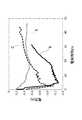
- Example 1 of this invention it is a figure which shows the time-dependent change of the electric current at the time of electrolytic reduction.
- 1 is an X-ray diffraction pattern of silicon obtained in Example 1 of the present invention. It is a scanning electron micrograph of the silicon obtained in Example 1 of the present invention.
- Example 5 of this invention it is a figure which shows the time-dependent change of the electric current at the time of electrolytic reduction.
- Examples 6 to 8 of the present invention it is a diagram showing the change with time of current during electrolytic reduction.
- Examples 9 to 11 of the present invention it is a diagram showing a change with time of current during electrolytic reduction. It is a schematic explanatory drawing of the electrolytic reduction apparatus used for the manufacturing method of the conventional silicon
- the method for producing silicon of the present invention is a method for producing silicon by electrolytic reduction of silicon dioxide in the presence of a molten salt, in which silicon dioxide is placed on a cathode made of silicon. The silicon dioxide is subjected to electrolytic reduction.
- silicon dioxide is used as a raw material.
- silicon dioxide include quartz, silicon dioxide sand, and amorphous silicon dioxide, but the present invention is not limited to such examples.
- amorphous silicon dioxide is preferred because of its high reduction rate.
- the amorphous silicon dioxide include amorphous silicon dioxide contained in diatomaceous earth. In general, diatomaceous earth contains amorphous silicon dioxide at a content of 80 to 90% by mass, but also contains, for example, clay components such as alumina.
- Amorphous silicon dioxide contained in diatomaceous earth unlike crystalline silicon dioxide contained in quartz and the like, has the property of being easily dissolved in an alkaline aqueous solution, so that amorphous silicon dioxide is dissolved in an alkaline aqueous solution. Thereafter, by repeating the operation of precipitating amorphous silicon dioxide by controlling the pH of the aqueous solution, amorphous silicon dioxide having a high purity of 99.9999% by mass or more can be prepared.
- the purity of silicon dioxide is preferably as high as possible from the viewpoint of producing silicon having high purity by electrolytic reduction of silicon dioxide.
- the content of impurities in silicon dioxide is preferably 100 ppm or less, more preferably 10 ppm or less, still more preferably 1 ppm or less, and particularly preferably 0. 0 ppm from the viewpoint of producing silicon having high purity by electrolytic reduction of silicon dioxide. 5 ppm or less.
- Examples of impurities in silicon dioxide include metals such as sodium, potassium, calcium, magnesium, aluminum, titanium, manganese, and iron, boron, phosphorus, and the like, but the present invention is limited to such examples. It is not a thing.
- Silicon dioxide is usually used as silicon dioxide particles.
- the lower limit of the particle diameter of the silicon dioxide particles is preferably 0.2 ⁇ m or more, more preferably 0.5 ⁇ m or more from the viewpoint of efficiently performing the electrolytic reduction of silicon dioxide, and the upper limit of the particle diameter of the silicon dioxide particles is From the viewpoint of efficiently carrying out the electrolytic reduction of silicon dioxide as in the above lower limit, it is preferably 2 ⁇ m or less.
- Silicon dioxide particles can be easily obtained commercially, for example, by refined SiO 2 particles manufactured by Taiheiyo Cement Co., Ltd.
- porous material for silicon dioxide used for electrolytic reduction it is preferable to use a porous material for silicon dioxide used for electrolytic reduction.
- a porous body the molded object shape
- Examples of the shape of the silicon dioxide molded body include a cylinder, a cube, a rectangular parallelepiped, a plate, a thin film, a sphere, and the like, but the present invention is not limited to only such examples.
- the size of the silicon dioxide molded body is not particularly limited, but from the viewpoint of efficiently performing electrolytic reduction of silicon dioxide, a cylindrical molded body having a diameter of about 5 to 30 mm and a thickness of about 1 to 10 mm. A cubic or cuboid shaped body having a side length of about 5 to 30 mm is preferred.
- the silicon dioxide molded body can be easily manufactured by, for example, compression molding.
- a silicon dioxide molded body is produced by compression molding, a porous molded body in which voids communicating with the surface are present inside the molded body is obtained. Since this porous molded body can be impregnated with the molten salt, the porous molded body has the advantage that the electrolytic reduction of silicon dioxide can be performed efficiently. Therefore, in the present invention, a porous molded body of silicon dioxide can be suitably used as silicon dioxide.
- a porous molded body of silicon dioxide can be produced, for example, by mixing silicon dioxide particles and an appropriate amount of water, filling the resulting mixture into a mold having a desired inner surface shape, and pressurizing. .
- the temperature is about 1000 to 1500 ° C. in an air atmosphere or an inert gas atmosphere such as nitrogen gas or argon gas. By heating to sinter, a sintered porous molded body can be produced.
- the porosity of the porous molded body of silicon dioxide is preferably 30% or more, more preferably 40% or more, and still more preferably, from the viewpoint of increasing the efficiency of electrolytic reduction of silicon dioxide by allowing molten salt to enter the inside. From the viewpoint of increasing the mechanical strength of the porous molded body itself and increasing the mechanical strength of silicon generated by electrolytic reduction of silicon dioxide, it is preferably 80% or less, more preferably 70% or less. More preferably, it is 65% or less.
- the particle size of the silicon dioxide particles is the sum of the electrical contact resistance generated between the silicon particles that are reduced and formed while being properly placed on the cathode, suppressing the scattering of particles due to convection in the molten salt. From the viewpoint of improving the electrolytic reduction efficiency of silicon dioxide by reducing the value, it is preferably 50 ⁇ m or more, more preferably 100 ⁇ m or more, still more preferably 200 ⁇ m or more, and even more preferably 300 ⁇ m or more. From the viewpoint of reducing the time required for the electrolytic reduction until, it is preferably 30 mm or less, more preferably 10 mm or less, and even more preferably 3 mm or less.
- the particle diameter of the silicon dioxide granular material is a value measured by a laser diffraction particle size distribution analyzer (manufactured by Nikkiso Co., Ltd., trade name: Microtrac MT3300II, solvent: water, dispersant: none). . Since voids exist between the particles constituting the granular material, the silicon dioxide granular material can be impregnated with the molten salt to the inside thereof, like the porous molded body of silicon dioxide. In addition, there is an advantage that the electrolytic reduction of silicon dioxide can be performed efficiently. Therefore, in the present invention, silicon dioxide particles can be suitably used as silicon dioxide.
- the silicon dioxide granules are produced, for example, by mixing silicon dioxide particles and an appropriate amount of water, filling the resulting mixture into a mold having a desired inner surface shape, pressurizing, and grinding if necessary. be able to.
- sintering the granular material after drying the granular material, by heating to a temperature of about 1000 to 1500 ° C. in an air atmosphere or an inert gas atmosphere such as nitrogen gas or argon gas, Sintered granules can be produced.
- the granular material may be a granular material pulverized after sintering.
- the granular material may be screened to make the particle diameter uniform.
- the present invention has one major feature in that silicon dioxide is electrolytically reduced in the presence of molten salt in a state where silicon dioxide is placed on a cathode made of silicon.
- silicon dioxide is electrolytically reduced in the presence of molten salt in a state where silicon dioxide is placed on a cathode made of silicon.
- a cathode made of silicon is used as the cathode.
- the cathode made of silicon means a cathode having at least a surface formed of silicon. Therefore, the cathode made of silicon may be composed only of silicon, or may be a composite in which the surface of a metal substrate such as molybdenum is covered with silicon. If necessary, silicon dioxide powder may be attached to the surface of the cathode.
- the purity of silicon used for the cathode is preferably 99.9% by mass or more, more preferably 99.99% by mass or more, and further preferably 99.999% by mass or more, from the viewpoint of increasing the purity of the obtained silicon. Especially preferably, it is 99.9999 mass% or more.
- the size of the cathode on which silicon dioxide is placed is not particularly limited as long as silicon dioxide can be placed on the cathode.
- silicon dioxide shaped bodies when one or a plurality of silicon dioxide shaped bodies are used as silicon dioxide, a size that allows any of the shaped bodies to be placed on the cathode is selected. Therefore, the size of the cathode is preferably determined as appropriate according to the size and number of silicon dioxides placed on the cathode.
- the shape of the cathode is not particularly limited, and examples of the shape of the cathode include a disk shape whose planar shape is a circle or an ellipse, a plate shape whose plane shape is a triangle, a rectangle, and other polygons. However, the present invention is not limited to such examples.
- the surface of the cathode on which silicon dioxide is placed preferably has a shape having a large contact area with silicon dioxide from the viewpoint of efficiently performing electrolytic reduction of silicon dioxide.
- the surface of the cathode on which silicon dioxide is placed is preferably planar.
- an uneven shape may be provided on the upper surface of the cathode on which silicon dioxide is placed, and a shape corresponding to the uneven shape may be formed on the bottom surface of the silicon dioxide molded body.
- the cathode is connected to a conductor, for example, and is connected to a power source via the conductor.
- Examples of the salt used for the molten salt include metal halides such as alkali metal halides and alkaline earth metal halides, but the present invention is not limited to such examples. These metal halides may be used alone or in combination of two or more.
- examples of the alkali metal include lithium, sodium, potassium, cesium and the like.
- examples of the alkaline earth metal include magnesium, calcium, strontium, barium and the like.
- a halogen atom which comprises a halide a fluorine atom, a chlorine atom, a bromine atom, an iodine atom etc. are mentioned, for example.
- the metal halide examples include alkali metal halides such as lithium chloride, sodium chloride, potassium chloride, and cesium chloride, and alkaline earth metal halides such as magnesium chloride, calcium chloride, strontium chloride, and barium chloride.
- alkali metal halides such as lithium chloride, sodium chloride, potassium chloride, and cesium chloride
- alkaline earth metal halides such as magnesium chloride, calcium chloride, strontium chloride, and barium chloride.
- the present invention is not limited to such examples.
- These metal halides may be used alone or in combination of two or more.
- lithium oxide, sodium chloride, magnesium chloride, and calcium chloride are preferable, and calcium chloride is more preferable because of high solubility of oxide ions.
- the temperature of the molten salt when electrolytically reducing silicon dioxide is preferably 500 ° C. or higher, more preferably 800 ° C. or higher, from the viewpoint of increasing the reduction efficiency of silicon dioxide. From the viewpoint of suppressing volatilization, it is usually preferably 1000 ° C. or lower, more preferably 900 ° C. or lower.
- anode examples include a carbon electrode, a graphite electrode, a glassy carbon electrode, a ferrite-based insoluble anode, and a titanium boride-based insoluble anode.
- the present invention is not limited to such examples.
- insoluble anodes such as ferrite-based insoluble anodes and titanium boride-based insoluble anodes are preferable from the viewpoint of avoiding contamination with impurities.
- the cathode potential at the time of electrolytic reduction of silicon dioxide so that the potential is higher than the potential at which cations derived from the molten salt precipitate from the melt.
- the cathodic potential differs depending on the type of the molten salt, and thus cannot be determined unconditionally. However, from the viewpoint of avoiding the bond between the metal generated by reduction of the cation derived from the molten salt and silicon, it is generally 0. 5V [vs.
- M n + / M (M is an alkali metal or alkaline earth metal deposited at the cathode limit of the molten salt, n is a valence of the alkali metal or alkaline earth metal)] or higher, preferably 0 more preferably .6V [(the M and n the same as) to M n + / M] is at least, from the viewpoint 1.2V [vs. M n + / M (M and n to improve the efficiency of electrolytic reduction and the The same)] is preferred.
- silicon dioxide is placed on the cathode, molten salt is placed in this electrolytic cell, and electrolytic reduction is performed. Silicon can be produced. At that time, when silicon dioxide is electrolytically reduced while supplying silicon dioxide on the cathode so that silicon dioxide is placed on the cathode, silicon can be continuously produced. It can be efficiently manufactured in large quantities.
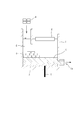
- FIG. 1 is a schematic explanatory view showing an embodiment of the electrolytic reduction apparatus used in the method for producing silicon of the present invention.
- a silicon dioxide plate 2 is disposed on the bottom of the inner surface of the electrolytic cell 1, and a cathode 3 made of silicon is disposed on the silicon dioxide plate 2.
- the electrolytic cell 1 is preferably formed of, for example, quartz or the like from the viewpoint of avoiding impurities from being mixed into generated silicon.
- the silicon dioxide plate 2 is preferably used from the viewpoint of improving the productivity of silicon, but in the present invention, silicon can be easily produced without using the silicon dioxide plate 2.
- the internal space of the electrolytic cell 1 is preferably replaced with an inert gas such as nitrogen gas or argon gas, for example.
- a silicon dioxide 4 is placed on the cathode 3.
- the present invention has one major feature in that the silicon dioxide 4 is electrolytically reduced while the silicon dioxide 4 is placed on the cathode 3.
- silicon dioxide can be continuously electrolytically reduced without taking the complicated operation of replacing the cathode with a new cathode after electrolytic reduction as in the prior art. Silicon can be produced efficiently.
- the silicon dioxide 4 shown in FIG. 1 has a pellet shape, but the present invention is not limited by the shape of the silicon dioxide 4.
- the silicon dioxide 4 is preferably brought into contact with the cathode 3 so that the contact area with the cathode 3 is as large as possible from the viewpoint of efficiently producing silicon. Therefore, it is preferable to place the silicon dioxide 4 on the cathode 3 so that the silicon dioxide 4 and the cathode 3 are in surface contact.
- a molten salt 5 is injected into the electrolytic cell 1, and the molten salt 5 is electrically connected to the cathode 3 in order to electrically connect the anode 6, the cathode 3 and a power source (not shown).
- the body 7 and the reference electrode 8 are immersed.
- the reference electrode 8 is used as necessary.
- the temperature of the molten salt 5 can be measured using a thermocouple (not shown) such as a chromel-alumel thermocouple, for example.
- FIG. 2 is a schematic explanatory view showing another embodiment of the electrolytic reduction apparatus used in the method for producing silicon of the present invention.
- a cathode 3 made of silicon is disposed at the bottom of the inner surface of the electrolytic cell 1.
- the electrolytic cell 1 is preferably formed of, for example, quartz or the like from the viewpoint of avoiding impurities from being mixed into generated silicon.
- the internal space of the electrolytic cell 1 is preferably replaced with an inert gas such as nitrogen gas or argon gas, for example.
- the silicon dioxide 4 is placed on the cathode 3.
- silicon dioxide 4 is electrolytically reduced with the silicon dioxide 4 placed on the cathode 3.
- silicon dioxide 4 is electrolytically reduced to generate silicon 9.
- silicon 9 is generated by adding silicon dioxide 4 further.
- the silicon dioxide 4 is placed on the cathode 3 via
- the silicon dioxide 4 may be placed directly on the cathode 3 so as to be in contact with the cathode 3, or on the cathode 3 through the generated silicon 9 as shown in FIG. 2. It may be placed.
- the produced silicon 9 can be recovered from the take-out port 1a, for example, by providing a take-out port 1a at the lower part of the electrolytic cell 1.
- silicon 9 produced by electrolytic reduction of silicon dioxide 4 while supplying silicon dioxide 4 from the upper part of electrolytic cell 1 is disposed at the lower part of electrolytic cell 1. Since the silicon dioxide 4 can be continuously electrolytically reduced because it can be recovered from the outlet 1a, the silicon 9 can be continuously and efficiently manufactured.
- the silicon dioxide 4 shown in FIG. 2 has the shape of a pellet like the silicon dioxide 4 shown in FIG. 1, the present invention is not limited by the shape of the silicon dioxide 4.
- the silicon dioxide 4 is preferably brought into contact with the cathode 3 so that the contact area with the cathode 3 is as large as possible from the viewpoint of efficiently producing the silicon 9. Therefore, in the embodiment shown in FIG. 2, it is preferable to place the silicon dioxide 4 on the cathode 3 or the produced silicon 9 so that the silicon dioxide 4 is in surface contact with the cathode 3 or the produced silicon 9.
- the molten salt 5 is injected into the electrolytic cell 1.
- the anode 6 is disposed on the upper part of the electrolytic cell 1, but may not necessarily be disposed on the upper part of the electrolytic cell 1, and may be immersed in the molten salt 5.
- the cathode 3 is electrically connected to a power source (not shown) through a conductor 7.
- the temperature of the molten salt 5 can be measured using a thermocouple (not shown) such as a chromel-alumel thermocouple, for example.
- a reference electrode (not shown) may be used as necessary, similarly to the embodiment shown in FIG.
- the anode 6 is immersed in the molten salt 5 in the molten salt 5 and the molten salt 5 is immersed in the molten salt.
- the silicon 9 can be manufactured efficiently. Further, new silicon dioxide 4 is supplied to the molten salt 5 from the upper part of the electrolytic cell 1 while recovering the generated silicon 9 from the outlet 1 a disposed at the lower part of the electrolytic cell 1, and the silicon dioxide 4 on the cathode 3. Therefore, the silicon 9 can be manufactured continuously and efficiently.
- the content of metal impurities in the silicon produced as described above is preferably 100 mass ppm (hereinafter referred to as “ppm”) when used for applications requiring high purity such as silicon for solar cells. ) Or less, more preferably 10 ppm or less, further preferably 1 ppm or less, still more preferably 0.5 ppm or less, and particularly preferably 0.1 ppm or less.
- ppm 100 mass ppm
- metal impurities include sodium, magnesium, aluminum, potassium, calcium, titanium, manganese, iron, and the like, but the present invention is not limited to such examples.
- the properties of a p-type semiconductor or an n-type semiconductor are added to silicon by adding an additive such as boron or phosphorus to silicon in a small amount. Can be granted.
- the total content of boron and phosphorus contained in silicon is preferably 1 ppm or less from the viewpoint of controlling the function as a semiconductor.
- the silicon obtained by the production method of the present invention as described above is useful, for example, as a photovoltaic power element for solar cells, a negative electrode material for lithium batteries, and a raw material for silicon compounds.
- Example 1 Raw material of molten salt As a raw material of molten salt, 400 g of calcium chloride (purity: 99% or more) was placed in a quartz crucible (inner diameter: 85 mm, height: 120 mm, thickness: 2.5 mm), and then 500 The product from which moisture was removed by vacuum drying at 1 ° C. for 1 day or longer was used.
- Silicon dioxide As silicon dioxide used in the electrolytic reduction, both were mixed at a rate of 1.5 g of water per 1 g of silicon dioxide powder (manufactured by Taiheiyo Cement Co., Ltd., refined silica powder), and the resulting mixture was obtained. A pellet having an outer diameter of 12 mm and a thickness of 3 mm was prepared by putting it in a mold and pressurizing it at a pressure of 1.5 ⁇ 10 3 kg / cm 2 (about 147 MPa), and then in an argon gas atmosphere at 1350 ° C. Silicon dioxide pellets obtained by sintering for 30 minutes at temperature were used.
- Electrolytic reduction operation and results thereof Electrolytic reduction of silicon dioxide was performed using the electrolytic reduction apparatus shown in FIG.
- Argon gas (purity: 99.995%) was allowed to flow into the internal space of the quartz electrolytic cell 1, and the inside of the electrolytic cell 1 was maintained in an argon gas atmosphere.
- the silicon dioxide pellets obtained above as silicon dioxide 4 are placed on the cathode 3, and the molten salt 5 of calcium chloride heated and melted at 850 ° C. is put in the electrolytic cell 1 in an amount of 400 g.
- Constant potential electrolysis was carried out at a potential of 0.8 V (vs.
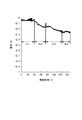
- FIG. 3 shows changes with time in the current during electrolytic reduction.
- the reduced part of the pellet was recovered and its X-ray diffraction was examined.
- X-ray diffraction was measured using an X-ray diffractometer (trade name: Ultimate IV, manufactured by Rigaku Corporation) with CuK ⁇ rays at a wavelength ( ⁇ ) of 1.5418 mm, a voltage of 40 kV, and a current of 40 mA.
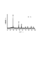
- the X-ray diffraction pattern is shown in FIG.
- FIG. 5 As shown in the scanning electron micrograph of FIG. 5, a needle-like structure having a diameter of about 1 ⁇ m, a columnar structure having a diameter of about 10 ⁇ m, and a lump structure in which particles are aggregated were confirmed in the silicon obtained above. Moreover, when elemental analysis of each region of X 1 , X 2, and X 3 shown in FIG. 5 was performed with an X-ray analyzer [trade name: Genesis, manufactured by EDAX], needle-like and columnar substances were Was also confirmed to be silicon. On the other hand, a large amount of oxygen was detected from the massive portion, suggesting that a relatively large amount of silicon dioxide was contained. From the above, it was confirmed that silicon having a needle-like or columnar structure was formed by electrolytic reduction of silicon dioxide as described above.
- the molybdenum content was less than 0.1 ppm
- the boron content was less than 1 ppm
- the phosphorus content was 1 ppm. Was less than.
- FIG. 2 shows an electrolytic reduction apparatus that can easily supply silicon dioxide continuously.
- An electrolytic reduction apparatus was used.
- silicon dioxide 4 the same silicon dioxide pellets as used in Example 1 were used. While conducting the electrolytic reduction of silicon dioxide 4 in the same manner as in Example 1, silicon dioxide pellets were put into the molten calcium chloride salt 5 from the upper part of the electrolytic cell 1 so that the silicon dioxide 4 was placed on the cathode 3. By doing so, the silicon dioxide 4 was supplied on the cathode 3, and the silicon dioxide 4 was electrolytically reduced.
- the silicon dioxide pellets were initially floating in the vicinity of the bath surface of the calcium chloride molten salt 5, but settled in the calcium chloride molten salt 5 after a while. Thereafter, in the same manner as in Example 1, when constant potential electrolysis was performed at a potential of 0.8 V (vs. Ca 2+ / Ca) for 58 hours, the amount of electricity supplied was the electricity required to reduce silicon dioxide 4. About 80% of the amount.
- the produced silicon was recovered from the outlet 1a disposed in the lower part of the electrolytic cell 1, washed in the same manner as in Example 1, and then the X-ray diffraction of the produced silicon 9 was examined.
- the diffraction lines derived from were clearly observed. Therefore, when the silicon dioxide 4 is electrolytically reduced while supplying the silicon dioxide 4 onto the cathode 3 so that the silicon dioxide 4 is placed on the cathode 3, the silicon 9 is continuously and efficiently supplied. It was confirmed that it could be manufactured.
- the content of impurities contained in the obtained silicon 9 was examined by glow discharge mass spectrometry, the content of molybdenum was less than 0.1 ppm, the content of boron was less than 1 ppm, and the content of phosphorus was 1 ppm. Was less than.
- Comparative Example 1 Silicon was produced according to the description in “Example 1” of JP-A-2006-321688. At that time, it is necessary to produce a cathode in which the silicon electrode and the porous silicon dioxide powder compact are in contact with each other by attaching the porous silicon dioxide powder compact to the silicon electrode rod. The operation was complicated. In addition, after electrolytic reduction of silicon dioxide, the cathode must be taken out of the electrolytic cell and replaced with a new cathode, so that the operation is complicated and the operation of electrolytic reduction of silicon dioxide must be temporarily interrupted. I had to.
- Example 1 and Example 2 as compared with Comparative Example 1, the complicated operation of attaching the porous silicon dioxide powder compact to the silicon electrode rod is unnecessary. It can be seen that can be efficiently electrolytically reduced. Moreover, according to Example 1 and Example 2, since silicon dioxide can be continuously supplied in an electrolytic cell and silicon can be manufactured continuously, it can be seen that silicon can be manufactured efficiently. Furthermore, according to Example 2, the silicon dioxide can be electrolytically reduced while supplying silicon dioxide onto the cathode so that silicon dioxide is placed on the cathode, and the generated silicon can be recovered. Since silicon can be produced continuously and efficiently, it can be seen that silicon can be produced continuously in large quantities.
- Example 3 In Example 1, electrolytic reduction was performed in the same manner as in Example 1 except that the cathode potential was changed from 0.8 V (vs. Ca 2+ / Ca) to 1.2 V (vs. Ca 2+ / Ca). . As a result, it was confirmed that silicon having a low impurity content can be efficiently produced as in Example 1.
- Example 4 In Example 2, electrolytic reduction was performed in the same manner as in Example 2 except that the cathode potential was changed from 0.8 V (vs. Ca 2+ / Ca) to 1.2 V (vs. Ca 2+ / Ca). . As a result, it was confirmed that silicon having a low impurity content can be produced as in Example 2 and that silicon can be produced continuously and efficiently.
- Example 5 In Example 1, except that the cathode potential was changed from 0.8 V (vs. Ca 2+ / Ca) to 0.7 V (vs. Ca 2+ / Ca) and the electrolysis time was changed from 150 hours to 80 hours.
- the electrolytic reduction was performed in the same manner as in Example 1.
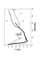
- FIG. 6 shows changes with time in the current during electrolytic reduction.
- the broken line indicates the change over time of the current during electrolytic reduction when the cathode potential is 0.7 V (vs. Ca 2+ / Ca) (Example 5)
- the solid line indicates that the cathode potential is 0.8 V (vs. Ca 2+ / Ca) shows the time-dependent change of the current during electrolytic reduction (Example 1).
- the reduction current (Example 5) during electrolysis when the cathode potential is 0.7 V (vs. Ca 2+ / Ca) shows that the cathode potential is 0.8 V (vs. Ca). 2 + / Ca), which is larger than the reduction current during electrolysis (Example 1), the reduction rate when the cathode potential is 0.7 V (vs. Ca 2+ / Ca) is It can be seen that the reduction rate is higher than that when the cathode potential is 0.8 V (vs. Ca 2+ / Ca). Further, according to Example 5, it was confirmed that silicon having a low impurity content can be efficiently produced as in Example 1.
- Examples 6-8 The silicon dioxide pellets used in Example 1 were pulverized, and the obtained pulverized product was sieved to obtain silicon dioxide granular materials having a particle diameter of 500 ⁇ m to 1 mm.
- Example 1 instead of placing silicon dioxide pellets on the cathode 3 as the silicon dioxide 4, placing the silicon dioxide particles obtained above on the cathode 3, and setting the cathode potential to 0.8V (Vs. Ca 2+ / Ca) to 0.7 V (vs. Ca 2+ / Ca) (Example 6), 0.6 V (vs. Ca 2+ / Ca) (Example 7) or 0.5 V (vs. Ca 2 + / Ca) (Example 8) and the electrolysis time was changed from 150 hours to 50 hours (Example 6), 48 hours (Example 7) or 31 hours (Example 8), Electrolytic reduction was carried out in the same manner as in Example 1.
- FIG. 7 shows changes with time in the current during electrolytic reduction.
- FIG. 7 shows changes with time in the current during electrolytic reduction.
- A is the time-dependent change in current during electrolytic reduction when the cathode potential is 0.7 V (vs. Ca 2+ / Ca)
- B is the cathode potential is 0.6 V (vs. Ca 2). + / Ca)
- the time-dependent change in current during electroreduction (Example 7)
- C is the time-dependent change in current during electroreduction when the cathode potential is 0.5 V (vs. Ca 2+ / Ca) (Example 8) is shown.
- Examples 9-11 Silicon dioxide powder (manufactured by Taiheiyo Cement Co., Ltd., refined silica powder) is mixed at a rate of 1.5 g of water per gram, and the resulting mixture is sintered at a temperature of 1350 ° C. for 30 minutes in an argon gas atmosphere. Thus, a silicon dioxide granular material was obtained. The obtained silicon dioxide granules are sieved to obtain silicon dioxide granules having a particle diameter of 5 to 7 mm (Example 9), silicon dioxide granules having a particle diameter of 500 ⁇ m to 1 mm (Example 10), and a particle diameter of 250 to 500 ⁇ m. Of silicon dioxide (Example 11) was obtained.
- Example 1 instead of placing silicon dioxide pellets as the silicon dioxide 4 on the cathode 3, the silicon dioxide granular material having a particle diameter of 5 to 7 mm obtained above (Example 9), obtained above.
- the silicon dioxide granular material having a particle diameter of 500 ⁇ m to 1 mm (Example 10) or the silicon dioxide granular material having a particle diameter of 250 to 500 ⁇ m obtained above (Example 11) was placed on the cathode 3, and the cathode potential was changed. Change from 0.8 V (vs. Ca 2+ / Ca) to 0.5 V (vs.
- FIG. 8 shows changes with time in the current during electrolytic reduction.
- A is the time-dependent change in current during electrolytic reduction when using silicon dioxide granules having a particle diameter of 5 to 7 mm (Example 9)
- B is silicon dioxide granules having a particle diameter of 500 ⁇ m to 1 mm.
- C shows the time-dependent change in current during electrolytic reduction (Example 11) when using silicon dioxide particles having a particle diameter of 250 to 500 ⁇ m.
- the silicon production method of the present invention it is not necessary to take out the cathode from the electrolytic cell after electrolytic reduction of silicon dioxide, and silicon can be produced by continuously electrolytic reduction of silicon dioxide. I understand.
Landscapes
- Chemical & Material Sciences (AREA)
- Organic Chemistry (AREA)
- Inorganic Chemistry (AREA)
- Engineering & Computer Science (AREA)
- Chemical Kinetics & Catalysis (AREA)
- Electrochemistry (AREA)
- Materials Engineering (AREA)
- Metallurgy (AREA)
- Silicon Compounds (AREA)
- Electrolytic Production Of Non-Metals, Compounds, Apparatuses Therefor (AREA)
- Electrolytic Production Of Metals (AREA)
Abstract
溶融塩の存在下で二酸化ケイ素を電解還元させることによってシリコンを製造する方法であって、シリコンからなる陰極上に二酸化ケイ素を載置させた状態で当該二酸化ケイ素を電解還元させることを特徴とするシリコンの製造方法が提供される。
Description
本発明は、シリコンの製造方法に関する。さらに詳しくは、例えば、太陽電池の光起電力の電力素子、リチウム電池の負極材料、シリコン化合物の原料などに有用なシリコンの製造方法に関する。
高純度を有するシリコンを安価で製造することができるシリコンの製造方法として、例えば、図9に示されるような電解装置を用い、その電解槽1に入れられた溶融塩5に二酸化ケイ素4からなる多孔質成形体の孔に挿入された陰極3および陽極6を浸漬した状態で、二酸化ケイ素4を溶融塩5中で電解還元させるシリコンの製造方法が提案されている(例えば、特許文献1の[請求項1]、図1など参照)。このシリコンの製造方法には、高純度を有するシリコンを安価で製造することができるという利点がある。
しかし、前記シリコンの製造方法では、二酸化ケイ素4の電解還元を継続して行なうためには、二酸化ケイ素4の電解還元後に電解槽1から陰極3自体を取り出し、当該陰極3を新たな陰極と交換しなければならないため、二酸化ケイ素4を連続して電解還元させることによってシリコンを製造することが困難である。
したがって、二酸化ケイ素の電解還元後に陰極を電解槽から取り出す必要がなく、二酸化ケイ素を連続して電解還元させることによってシリコンを製造することができるシリコンの製造方法の開発が望まれている。
本発明は、前記従来技術に鑑みてなされたものであり、二酸化ケイ素の電解還元後に陰極を電解槽から取り出す必要がなく、二酸化ケイ素を連続して電解還元させることによってシリコンを製造することができるシリコンの製造方法を提供することを課題とする。
本発明は、
(1) 溶融塩の存在下で二酸化ケイ素を電解還元させることによってシリコンを製造する方法であって、シリコンからなる陰極上に二酸化ケイ素を載置させた状態で当該二酸化ケイ素を電解還元させることを特徴とするシリコンの製造方法、
(2) 陰極上で二酸化ケイ素が載置されるように二酸化ケイ素を陰極上に供給しながら当該二酸化ケイ素を電解還元させる前記(1)に記載のシリコンの製造方法、および
(3) 二酸化ケイ素として、二酸化ケイ素の多孔質体を用いる前記(1)または(2)に記載のシリコンの製造方法
に関する。
(1) 溶融塩の存在下で二酸化ケイ素を電解還元させることによってシリコンを製造する方法であって、シリコンからなる陰極上に二酸化ケイ素を載置させた状態で当該二酸化ケイ素を電解還元させることを特徴とするシリコンの製造方法、
(2) 陰極上で二酸化ケイ素が載置されるように二酸化ケイ素を陰極上に供給しながら当該二酸化ケイ素を電解還元させる前記(1)に記載のシリコンの製造方法、および
(3) 二酸化ケイ素として、二酸化ケイ素の多孔質体を用いる前記(1)または(2)に記載のシリコンの製造方法
に関する。
本発明のシリコンの製造方法によれば、二酸化ケイ素の電解還元後に陰極を電解槽から取り出す必要がなく、二酸化ケイ素を連続して電解還元させることによってシリコンを製造することができるという優れた効果が奏される。
本発明のシリコンの製造方法は、前記したように、溶融塩の存在下で二酸化ケイ素を電解還元させることによってシリコンを製造する方法であり、シリコンからなる陰極上に二酸化ケイ素を載置させた状態で当該二酸化ケイ素を電解還元させることを特徴とする。
特許文献1に記載のシリコンの製造方法によれば、高純度を有するシリコンを安価で製造することができるという優れた利点を有する。しかし、本発明者らは、前記シリコンの製造方法よりもさらに二酸化ケイ素を効率よく電解還元させることができるシリコンの製造方法を開発するべく鋭意研究を重ねた結果、特許文献1に記載のように多孔質二酸化ケイ素粉末成形体に設けられた孔内にシリコン電極棒が挿入された状態で二酸化ケイ素を溶融塩中で電解還元させるのではなく、シリコンからなる陰極上に二酸化ケイ素を載置させた状態で当該二酸化ケイ素を電解還元させた場合には、二酸化ケイ素の電解還元後に陰極を電解槽から取り出して新たな陰極と交換するという煩雑な操作を採らなくても二酸化ケイ素を連続して供給するだけで、当該二酸化ケイ素の電解還元により、シリコンを連続して製造することができることが見出された。本発明は、かかる知見に基づいて完成されたものである。
本発明のシリコンの製造方法において、原料として二酸化ケイ素が用いられる。二酸化ケイ素としては、例えば、石英、二酸化ケイ素サンド、アモルファス二酸化ケイ素などが挙げられるが、本発明は、かかる例示のみに限定されるものではない。これらの二酸化ケイ素のなかでは、還元速度が高いことから、アモルファス二酸化ケイ素が好ましい。アモルファス二酸化ケイ素としては、例えば、珪藻土などに含まれているアモルファス二酸化ケイ素などが挙げられる。一般に、珪藻土には、アモルファス二酸化ケイ素が80~90質量%の含有率で含まれているが、それ以外にも、例えば、アルミナなどの粘土成分が含まれている。珪藻土に含まれているアモルファス二酸化ケイ素は、石英などに含まれている結晶性二酸化ケイ素とは相違して、アルカリ水溶液に容易に溶解する性質を有することから、アモルファス二酸化ケイ素をアルカリ水溶液に溶解させた後、当該水溶液のpHを制御することによってアモルファス二酸化ケイ素を析出させる操作を繰り返すことにより、99.9999質量%以上の高純度を有するアモルファス二酸化ケイ素を調製することができる。
二酸化ケイ素の純度は、二酸化ケイ素を電解還元させることによって高純度を有するシリコンを製造する観点から、できるだけ高いことが好ましい。二酸化ケイ素における不純物の含有率は、二酸化ケイ素を電解還元させることによって高純度を有するシリコンを製造する観点から、好ましくは100ppm以下、より好ましくは10ppm以下、さらに好ましくは1ppm以下、特に好ましくは0.5ppm以下である。なお、二酸化ケイ素における不純物としては、例えば、ナトリウム、カリウム、カルシウム、マグネシウム、アルミニウム、チタン、マンガン、鉄などの金属、ホウ素、リンなどが挙げられるが、本発明は、かかる例示のみに限定されるものではない。
二酸化ケイ素は、通常、二酸化ケイ素粒子として用いられる。二酸化ケイ素粒子の粒子径の下限値は、二酸化ケイ素の電解還元を効率よく行なう観点から、好ましくは0.2μm以上、より好ましくは0.5μm以上であり、二酸化ケイ素粒子の粒子径の上限値は、前記下限値と同様に二酸化ケイ素の電解還元を効率よく行なう観点から、好ましくは2μm以下である。二酸化ケイ素粒子は、例えば、太平洋セメント(株)製、精製SiO2粒子などにより、商業的に容易に入手することができる。
電解還元に用いられる二酸化ケイ素には、多孔質体を用いることが好ましい。多孔質体としては、例えば、所望の形状となるように成形した成形体、粒子同士が凝集または結合した粒状物などが挙げられる。
二酸化ケイ素の成形体の形状としては、例えば、円柱、立方体、直方体、プレート、薄膜、球などが挙げられるが、本発明は、かかる例示のみに限定されるものではない。二酸化ケイ素の成形体の大きさは、特に限定されないが、二酸化ケイ素の電解還元を効率よく行なう観点から、直径が5~30mm程度であり、厚さが1~10mm程度である円柱形状の成形体、一辺の長さが5~30mm程度である立方体状または直方体状の成形体などが好ましい。
二酸化ケイ素の成形体は、例えば、圧縮成形などによって容易に製造することができる。二酸化ケイ素の成形体を圧縮成形によって製造した場合、表面と連通した空隙が成形体の内部に存在する多孔質成形体が得られる。この多孔質成形体は、その内部にまで溶融塩を含浸させることができるので、二酸化ケイ素の電解還元を効率よく行なうことができるという利点を有する。したがって、本発明においては、二酸化ケイ素として二酸化ケイ素の多孔質成形体を好適に用いることができる。
二酸化ケイ素の多孔質成形体は、例えば、二酸化ケイ素粒子と適量の水とを混合し、得られた混合物を所望の内面形状を有する成形型内に充填し、加圧することによって製造することができる。なお、二酸化ケイ素の多孔質成形体を圧縮成形によって製造する場合、得られる多孔質成形体の機械的強度を高める観点から、当該多孔質成形体を焼結することが好ましい。二酸化ケイ素の多孔質成形体を焼結する場合には、前記多孔質成形体を乾燥させた後、大気雰囲気中または窒素ガス、アルゴンガスなどの不活性ガス雰囲気中で1000~1500℃程度の温度に加熱することにより、焼結された多孔質成形体を製造することができる。
二酸化ケイ素の多孔質成形体の空隙率は、その内部に溶融塩を浸入させることによって二酸化ケイ素の電解還元の効率を高める観点から、好ましくは30%以上、より好ましくは40%以上、さらに好ましくは50%以上であり、当該多孔質成形体自体の機械的強度を高めるとともに二酸化ケイ素の電解還元によって生成するシリコンの機械的強度を高める観点から、好ましくは80%以下、より好ましくは70%以下、さらに好ましくは65%以下である。
二酸化ケイ素の粒状物の粒子径は、溶融塩中における対流などによる粒状物の飛散を抑制し、陰極上に適切に載置させるとともに還元生成したシリコン粒状物間に発生する電気的接触抵抗の合計値を低減させて二酸化ケイ素の電解還元効率を向上させる観点から、好ましくは50μm以上、より好ましくは100μm以上、さらに好ましくは200μm以上、さらに一層好ましくは300μm以上であり、二酸化ケイ素の粒状物の内部までの電解還元に要する時間を低減させる観点から、好ましくは30mm以下、より好ましくは10mm以下、さらに好ましくは3mm以下である。ここで、二酸化ケイ素の粒状物の粒子径は、レーザー回折式粒度分布計〔日機装(株)製、商品名:マイクロトラックMT3300II、溶媒:水、分散剤:なし〕によって測定したときの値である。粒状物を構成する粒子間には、空隙が存在していることから、二酸化ケイ素の粒状物は、二酸化ケイ素の多孔質成形体と同様に、その内部にまで溶融塩を含浸させることができるので、二酸化ケイ素の電解還元を効率よく行なうことができるという利点を有する。したがって、本発明においては、二酸化ケイ素として二酸化ケイ素の粒状物を好適に用いることができる。
二酸化ケイ素の粒状物は、例えば、二酸化ケイ素粒子と適量の水とを混合し、得られた混合物を所望の内面形状を有する成形型内に充填し、加圧し、必要により粉砕することによって製造することができる。なお、前記で得られた粒状物は、機械的強度を高める観点から、焼結することが好ましい。前記粒状物を焼結する場合には、前記粒状物を乾燥させた後、大気雰囲気中または窒素ガス、アルゴンガスなどの不活性ガス雰囲気中で1000~1500℃程度の温度に加熱することにより、焼結された粒状物を製造することができる。前記粒状物は、焼結後に粉砕した粒状物であってもよい。また、前記粒状物は、篩にかけて粒子径を揃えてもよい。
本発明においては、二酸化ケイ素をシリコンからなる陰極上に載置させた状態で、溶融塩の存在下で二酸化ケイ素を電解還元させる点に、1つの大きな特徴がある。本発明では、前記操作が採られているので、二酸化ケイ素を連続して電解還元させることによってシリコンを製造することができることから、シリコンを効率よく製造することができる。
本発明においては、陰極には、シリコンからなる陰極が用いられる。本明細書において、前記シリコンからなる陰極は、少なくとも表面がシリコンで形成されている陰極を意味する。したがって、前記シリコンからなる陰極は、シリコンのみで構成されていてもよく、あるいはモリブデンなどの金属基材の表面がシリコンで被覆された複合体であってもよい。なお、陰極の表面には、必要により、二酸化ケイ素粉末が付着されていてもよい。
陰極に用いられるシリコンに不純物が含まれている場合、二酸化ケイ素を電解還元したときに当該不純物が、二酸化ケイ素の電解還元によって生成するシリコンに混入するおそれがある。したがって、陰極に用いられるシリコンの純度は、得られるシリコンの純度を高める観点から、好ましくは99.9質量%以上、より好ましくは99.99質量%以上、さらに好ましくは99.999質量%以上、特に好ましくは99.9999質量%以上である。
二酸化ケイ素が載置される陰極の大きさは、当該陰極上に二酸化ケイ素を載置させることができるのであればよく、特に限定されない。例えば、二酸化ケイ素として1個または複数個の二酸化ケイ素の成形体を用いる場合には、当該成形体のいずれもが陰極上に載置することができる大きさが選択される。したがって、陰極の大きさは、陰極上に載置される二酸化ケイ素の大きさおよび個数に応じて適宜決定することが好ましい。また、陰極の形状についても特に限定がなく、陰極の形状としては、例えば、平面形状が円形ないし楕円形である円盤状、平面形状が三角形、四角形、その他の多角形である板状などが挙げられるが、本発明は、かかる例示のみに限定されるものではない。
二酸化ケイ素が載置される陰極の表面は、二酸化ケイ素の電解還元を効率よく行なう観点から、二酸化ケイ素との接触面積が大きい形状を有することが好ましい。例えば、二酸化ケイ素として平面状の底面を有する二酸化ケイ素の成形体を用いる場合には、二酸化ケイ素が載置される陰極の表面は、平面状であることが好ましい。また、二酸化ケイ素が載置される陰極の上面に凹凸形状を設けておき、この凹凸形状に対応する形状を二酸化ケイ素の成形体の底面に形成させてもよい。このように陰極の上面および二酸化ケイ素の成形体の底面に互いに対応する凹凸形状を設けた場合には、二酸化ケイ素の電解還元を効率よく行なうことができるだけでなく、二酸化ケイ素の成形体を陰極の所定位置に固定することができるとともに、二酸化ケイ素の成形体が陰極から滑落することを防止することができるという利点がある。陰極は、例えば、導電体と接続され、当該導電体を介して電源に接続される。
溶融塩に用いられる塩としては、例えば、アルカリ金属ハロゲン化物、アルカリ土類金属ハロゲン化物などの金属ハロゲン化物が挙げられるが、本発明は、かかる例示のみに限定されるものではない。これらの金属ハロゲン化物は、それぞれ単独で用いてもよく、2種類以上を併用してもよい。アルカリ金属ハロゲン化物において、アルカリ金属としては、例えば、リチウム、ナトリウム、カリウム、セシウムなどが挙げられる。アルカリ土類金属ハロゲン化物において、アルカリ土類金属としては、例えば、マグネシウム、カルシウム、ストロンチウム、バリウムなどが挙げられる。また、ハロゲン化物を構成するハロゲン原子としては、例えば、フッ素原子、塩素原子、臭素原子、ヨウ素原子などが挙げられる。金属ハロゲン化物の具体例としては、塩化リチウム、塩化ナトリウム、塩化カリウム、塩化セシウムなどのアルカリ金属ハロゲン化物、塩化マグネシウム、塩化カルシウム、塩化ストロンチウム、塩化バリウムなどのアルカリ土類金属ハロゲン化物などが挙げられるが、本発明は、かかる例示のみに限定されるものではない。これらの金属ハロゲン化物は、それぞれ単独で用いてもよく、2種類以上を併用してもよい。金属ハロゲン化物のなかでは、酸化物イオンの溶解度が高いことから、塩化リチウム、塩化ナトリウム、塩化マグネシウムおよび塩化カルシウムが好ましく、塩化カルシウムがより好ましい。
二酸化ケイ素を電解還元させるときの溶融塩の温度は、二酸化ケイ素の還元効率を高める観点から、好ましくは500℃以上、より好ましくは800℃以上であり、溶融塩の種類によって異なるが、溶融塩の揮発を抑制する観点から、通常、好ましくは1000℃以下、より好ましくは900℃以下である。
陽極としては、例えば、炭素電極、グラファイト電極、グラッシーカーボン電極、フェライト系不溶性陽極、ホウ化チタン系不溶性陽極などが挙げられるが、本発明は、かかる例示のみに限定されるものではない。これらの陽極のなかでは、不純物の混入を回避する観点から、フェライト系不溶性陽極、ホウ化チタン系不溶性陽極などの不溶性陽極が好ましい。
二酸化ケイ素を電解還元させる際の陰極電位は、溶融塩に由来のカチオンが溶融物から析出する電位よりも貴な電位となるように設定することが好ましい。陰極電位は、溶融塩の種類によって異なるため一概には決定することができないが、通常、溶融塩に由来のカチオンが還元されて生成した金属とシリコンとが結合することを回避する観点から0.5V〔対Mn+/M(Mは溶融塩のカソード限界で析出するアルカリ金属またはアルカリ土類金属、nはアルカリ金属またはアルカリ土類金属の価数を示す)〕以上であることが好ましく、0.6V〔対Mn+/M(Mおよびnは前記と同じ)〕以上であることがより好ましく、電解還元の効率を高める観点から1.2V〔対Mn+/M(Mおよびnは前記と同じ)〕以下であることが好ましい。
本発明のシリコンの製造方法では、例えば、電解槽内を不活性ガス雰囲気とした後、陰極上に二酸化ケイ素を載置し、溶融塩をこの電解槽内に入れ、電解還元を行なうことにより、シリコンを製造することができる。その際、陰極上で二酸化ケイ素が載置されるように二酸化ケイ素を陰極上に供給しながら当該二酸化ケイ素を電解還元させた場合には、シリコンを連続して製造することができることから、シリコンを大量に効率よく製造することができる。
本発明のシリコンの製造方法は、例えば、図1に示される電解還元装置を用いることによって実施することができる。図1は、本発明のシリコンの製造方法に用いられる電解還元装置の一実施態様を示す概略説明図である。
図1において、電解槽1の内面底部に二酸化ケイ素板2が配置され、当該二酸化ケイ素板2の上にシリコンからなる陰極3が配置されている。電解槽1は、生成するシリコンに不純物が混入することを回避する観点から、例えば、石英などで形成されていることが好ましい。二酸化ケイ素板2は、シリコンの生産性向上の観点から用いられていることが好ましいが、本発明においては、二酸化ケイ素板2を用いなくてもシリコンを容易に製造することができる。電解槽1の内部空間は、例えば、窒素ガス、アルゴンガスなどの不活性ガスで置換されていることが好ましい。
陰極3上には二酸化ケイ素4が載置されている。本発明においては、前記したように、陰極3上に二酸化ケイ素4を載置させた状態で二酸化ケイ素4を電解還元させる点に1つの大きな特徴がある。本発明では、当該操作が採られているので、従来のように電解還元後に陰極を新たな陰極と交換するという煩雑な操作を採らなくても二酸化ケイ素を連続して電解還元させることができるので、シリコンを効率よく製造することができる。
図1に示される二酸化ケイ素4は、ペレットの形状を有するが、本発明は、二酸化ケイ素4の形状によって限定されるものではない。なお、二酸化ケイ素4は、シリコンを効率よく製造する観点から、陰極3との接触面積ができるだけ大きくなるように陰極3と接触させることが好ましい。したがって、二酸化ケイ素4と陰極3とが面接触するように、陰極3上に二酸化ケイ素4を載置させることが好ましい。
電解槽1の内部には溶融塩5が注入されており、当該溶融塩5には陽極6、陰極3と電源(図示せず)とを電気的に接続するために陰極3と接続された導電体7および参照電極8が浸漬されている。参照電極8は、必要により用いられる。参照電極8としては、例えば、白金線などを用いることができる。溶融塩5の温度は、例えば、クロメル・アルメル熱電対などの熱電対(図示せず)を用いて測定することができる。
また、本発明においては、図1に示された電解還元装置以外にも、例えば、図2に示される電解還元装置を用いて二酸化ケイ素の電解還元を連続的に行なうことができる。図2は、本発明のシリコンの製造方法に用いられる電解還元装置の他の一実施態様を示す概略説明図である。
図2において、電解槽1の内面底部にシリコンからなる陰極3が配置されている。電解槽1は、生成するシリコンに不純物が混入することを回避する観点から、例えば、石英などで形成されていることが好ましい。電解槽1の内部空間は、例えば、窒素ガス、アルゴンガスなどの不活性ガスで置換されていることが好ましい。
陰極3上には二酸化ケイ素4が載置される。陰極3上に二酸化ケイ素4を載置させた状態で二酸化ケイ素4を電解還元させたとき、二酸化ケイ素4が電解還元されることにより、シリコン9が生成する。なお、図2に示される実施態様では、陰極3上に載置された二酸化ケイ素4が電解還元されることによってシリコン9が生成した後に、さらに二酸化ケイ素4を添加することにより、生成したシリコン9を介して陰極3上に二酸化ケイ素4が載置されている。本発明においては、二酸化ケイ素4は、陰極3と接触するように陰極3上に直接載置されていてもよく、あるいは図2に示されるように、生成したシリコン9を介して陰極3上に載置されていてもよい。生成したシリコン9は、例えば、電解槽1の下部に取出口1aを配設しておき、この取出口1aから回収することができる。
図2に示される電解還元装置を用いた場合には、電解槽1の上部から二酸化ケイ素4を補給しながら二酸化ケイ素4の電解還元によって生成したシリコン9を電解槽1の下部に配設された取出口1aから回収することができるので、二酸化ケイ素4を連続的に電解還元させることができることから、シリコン9を連続して効率よく製造することができる。
図2に示される二酸化ケイ素4は、図1に示される二酸化ケイ素4と同様に、ペレットの形状を有するが、本発明は、二酸化ケイ素4の形状によって限定されるものではない。なお、二酸化ケイ素4は、シリコン9を効率よく製造する観点から、陰極3との接触面積ができるだけ大きくなるように陰極3と接触させることが好ましい。したがって、図2に示される実施態様では、二酸化ケイ素4は、陰極3または生成したシリコン9と面接触するように、陰極3または生成したシリコン9上に二酸化ケイ素4を載置させることが好ましい。
電解槽1の内部には溶融塩5が注入されている。陽極6は、図2に示されるように電解槽1の上部に配設されているが、必ずしも電解槽1の上部に配設されていなくてもよく、溶融塩5中に浸漬されていてもよい。陰極3は、導電体7を介して電源(図示せず)と電気的に接続される。溶融塩5の温度は、例えば、クロメル・アルメル熱電対などの熱電対(図示せず)を用いて測定することができる。また、図2に示される実施態様では、図1に示される実施態様と同様に、必要により参照電極(図示せず)が用いられていてもよい。
以上説明したように、図2に示される電解還元装置を用いた場合には、溶融塩5が入れられた電解槽1内に、当該溶融塩5に陽極6を溶融塩に浸漬し、シリコンからなる陰極3上に二酸化ケイ素4を載置した状態で二酸化ケイ素4の電解還元を行なうことにより、シリコン9を効率よく製造することができる。また、生成したシリコン9を電解槽1の下部に配設された取出口1aから回収しながら電解槽1の上部から新たな二酸化ケイ素4を溶融塩5に供給し、陰極3上に二酸化ケイ素4を載置させることができるので、シリコン9を連続的に効率よく製造することができる。
前記のようにして製造されたシリコン中の金属不純物の含有率は、太陽電池用シリコンなどの高純度が要求される用途に使用する場合には、好ましくは100質量ppm(以下、「ppm」という)以下、より好ましくは10ppm以下、さらに好ましくは1ppm以下、さらに一層好ましくは0.5ppm以下、特に好ましくは0.1ppm以下である。金属不純物としては、例えば、ナトリウム、マグネシウム、アルミニウム、カリウム、カルシウム、チタン、マンガン、鉄などが挙げられるが、本発明は、かかる例示のみに限定されるものではない。
また、本発明の製造方法によって得られるシリコンを用いて半導体を製造する場合には、ホウ素やリンなどの添加物を少量でシリコンに加えることにより、p型半導体またはn型半導体の性質をシリコンに付与することができる。この場合、シリコンに含まれるホウ素およびリンの合計含有率は、半導体としての機能を制御する観点から、1ppm以下であることが好ましい。
以上のようにして本発明の製造方法によって得られるシリコンは、例えば、太陽電池の光起電力の電力素子、リチウム電池の負極材料、シリコン化合物の原料などに有用である。
次に、本発明を実施例に基づいてさらに詳細に説明するが、本発明は、かかる実施例のみに限定されるものではない。
実施例1
(1)溶融塩の原料
溶融塩の原料として、塩化カルシウム(純度:99%以上)400gを石英製るつぼ(内径:85mm、高さ:120mm、厚さ:2.5mm)に入れた後、500℃で1日間以上真空乾燥を行なうことにより、水分の除去を行なったものを用いた。
(1)溶融塩の原料
溶融塩の原料として、塩化カルシウム(純度:99%以上)400gを石英製るつぼ(内径:85mm、高さ:120mm、厚さ:2.5mm)に入れた後、500℃で1日間以上真空乾燥を行なうことにより、水分の除去を行なったものを用いた。
(2)二酸化ケイ素
電解還元の際に用いられる二酸化ケイ素として、二酸化ケイ素粉末〔太平洋セメント(株)製、精製シリカ粉末〕1gあたり水1.5gの割合で両者を混合し、得られた混合物を成形型内に入れ、1.5×10³kg/cm2(約147MPa)の圧力で加圧することにより、外径12mm、厚さ3mmのペレットを作製した後、アルゴンガス雰囲気中で1350℃の温度で30分間焼結することによって得られた二酸化ケイ素ペレットを用いた。
電解還元の際に用いられる二酸化ケイ素として、二酸化ケイ素粉末〔太平洋セメント(株)製、精製シリカ粉末〕1gあたり水1.5gの割合で両者を混合し、得られた混合物を成形型内に入れ、1.5×10³kg/cm2(約147MPa)の圧力で加圧することにより、外径12mm、厚さ3mmのペレットを作製した後、アルゴンガス雰囲気中で1350℃の温度で30分間焼結することによって得られた二酸化ケイ素ペレットを用いた。
(3)電極
陰極には板状のシリコン電極〔(株)ジャパンメタルサービス製〕を用い、陽極にはグラファイト棒〔東海カーボン(株)製、直径:5mm〕を用いた。また、参照極には直径1mmの白金線を用いた。
陰極には板状のシリコン電極〔(株)ジャパンメタルサービス製〕を用い、陽極にはグラファイト棒〔東海カーボン(株)製、直径:5mm〕を用いた。また、参照極には直径1mmの白金線を用いた。
(4)電解還元操作およびその結果
図1に示される電解還元装置を用いて二酸化ケイ素の電解還元を行なった。石英製の電解槽1の内部空間にアルゴンガス(純度99・995%)を流し、この電解槽1内をアルゴンガス雰囲気に保った。陰極3上に二酸化ケイ素4として前記で得られた二酸化ケイ素ペレットを載置し、850℃に加熱溶融させた塩化カルシウムの溶融塩5を400gの量で電解槽1内に入れ、同温度で陰極電位0.8V(対Ca2+/Ca)にて150時間定電位電解を行ない、残余電流による電流効率の低下を考慮して還元率110%相当の電気量を通電した。ここで、還元率は、式:
〔還元率(%)〕=〔(実際の電解を行なう際に要した電気量)/(理論上シリコンを生成させるのに必要な電気量)〕×100
にしたがって算出した。電解還元は、約40時間ごとに4回に分割して行ない、電解の休止時には開回路電位で静置した。電解還元時の電流の経時変化を図3に示す。
図1に示される電解還元装置を用いて二酸化ケイ素の電解還元を行なった。石英製の電解槽1の内部空間にアルゴンガス(純度99・995%)を流し、この電解槽1内をアルゴンガス雰囲気に保った。陰極3上に二酸化ケイ素4として前記で得られた二酸化ケイ素ペレットを載置し、850℃に加熱溶融させた塩化カルシウムの溶融塩5を400gの量で電解槽1内に入れ、同温度で陰極電位0.8V(対Ca2+/Ca)にて150時間定電位電解を行ない、残余電流による電流効率の低下を考慮して還元率110%相当の電気量を通電した。ここで、還元率は、式:
〔還元率(%)〕=〔(実際の電解を行なう際に要した電気量)/(理論上シリコンを生成させるのに必要な電気量)〕×100
にしたがって算出した。電解還元は、約40時間ごとに4回に分割して行ない、電解の休止時には開回路電位で静置した。電解還元時の電流の経時変化を図3に示す。
図3に示されるように、電解の進行とともに還元電流の増加が認められ、電解休止後の再通電時には、大きな還元電流が観測された。また、還元電流が経時とともに徐々に増加しているが、これは、二酸化ケイ素からシリコンへの還元の進行に伴い、二酸化ケイ素とシリコンとの接触面積が増大し、有効反応面積が増大することに基づくものと考えられる。
電解還元操作後のペレットを目視で観察したところ、その表面が黒色の多孔質体に変化しており、シリコンに還元されている部分が認められたが、その内部は、二酸化ケイ素の状態のままであった。このことから、本来、表面の還元が終了し、ペレットの内部方向に還元が進行する場合、反応が遅くなり、電流値が減少するものと考えられる。
次に、電解終了後の試料を蒸留水で洗浄した後、酸洗浄液〔蒸留水:1M塩酸 水溶液:30%過酸化水素水(容量比)=5:1:1〕で超音波洗浄を行なった。洗浄後、ペレットの還元された部分を回収し、そのX線回折を調べた。X線回折は、X線回折装置〔(株)リガク製、商品名:Ultima IV〕を用い、CuKα線にて波長(λ)1.5418Å、電圧40kV、電流40mAにて測定した。そのX線回折図を図4に示す。
図4に示された結果から、二酸化ケイ素に由来の回折線が微弱であり、シリコンの回折線が明瞭に現れていることから、実施例1によれば、二酸化ケイ素をシリコンに効率よく還元させることができることが確認された。
次に、前記で得られたシリコンを走査型電子顕微鏡〔(株)キーエンス製、品番:VE-8800〕で観察した。その結果を図5に示す。図5の走査型電子顕微鏡写真に示されるように、前記で得られたシリコンに、直径1μm程度の針状構造、直径10μm程度の柱状構造および粒子が凝集した塊伏構造が確認された。また、図5に示されるX1、X2およびX3の各領域の元素分析をX線分析装置〔EDAX社製、商品名:Genesis〕で行なったところ、針状および柱状の物質は、いずれもシリコンであることが確認された。一方、塊状の部分からは酸素が多く検出され、二酸化ケイ素が比較的多く含まれていることが示唆された。以上のことから、前記のようにして、二酸化ケイ素の電解還元を行なうことにより、針状または柱状の構造を有するシリコンが形成されることが確認された。
次に、得られたシリコンに含まれている不純物の含有率をグロー放電質量分析によって調べたところ、モリブデンの含有率は0.1ppm未満、ホウ素の含有率は1ppm未満、リンの含有率は1ppm未満であった。
実施例2
連続的に二酸化ケイ素の還元を行なうためには、二酸化ケイ素を継続的に供給することが望まれることから、二酸化ケイ素を継続的に供給することが容易な電解還元装置として、図2に示される電解還元装置を用いた。二酸化ケイ素4として、実施例1で用いたのと同様の二酸化ケイ素ペレットを用いた。実施例1と同様にして二酸化ケイ素4の電解還元を行ないながら、陰極3上で二酸化ケイ素4が載置されるように二酸化ケイ素ペレットを電解槽1の上部から塩化カルシウムの溶融塩5中に投入することによって二酸化ケイ素4を陰極3上に供給し、当該二酸化ケイ素4を電解還元させた。その結果、二酸化ケイ素ペレットは当初、塩化カルシウムの溶融塩5の浴面付近に浮遊していたが、しばらくしてから塩化カルシウムの溶融塩5中に沈降した。その後、実施例1と同様にして、0.8V(対Ca2+/Ca)の電位で58時間定電位電解を行なったところ、その通電量は、二酸化ケイ素4を還元させるのに必要な電気量の約80%であった。
連続的に二酸化ケイ素の還元を行なうためには、二酸化ケイ素を継続的に供給することが望まれることから、二酸化ケイ素を継続的に供給することが容易な電解還元装置として、図2に示される電解還元装置を用いた。二酸化ケイ素4として、実施例1で用いたのと同様の二酸化ケイ素ペレットを用いた。実施例1と同様にして二酸化ケイ素4の電解還元を行ないながら、陰極3上で二酸化ケイ素4が載置されるように二酸化ケイ素ペレットを電解槽1の上部から塩化カルシウムの溶融塩5中に投入することによって二酸化ケイ素4を陰極3上に供給し、当該二酸化ケイ素4を電解還元させた。その結果、二酸化ケイ素ペレットは当初、塩化カルシウムの溶融塩5の浴面付近に浮遊していたが、しばらくしてから塩化カルシウムの溶融塩5中に沈降した。その後、実施例1と同様にして、0.8V(対Ca2+/Ca)の電位で58時間定電位電解を行なったところ、その通電量は、二酸化ケイ素4を還元させるのに必要な電気量の約80%であった。
次に、生成したシリコンを電解槽1の下部に配設された取出口1aから回収し、実施例1と同様にして洗浄した後、生成したシリコン9のX線回折を調べたところ、シリコン9に由来の回折線が明瞭に観測された。このことから、陰極3上で二酸化ケイ素4が載置されるように二酸化ケイ素4を陰極3上に供給しながら当該二酸化ケイ素4を電解還元させた場合には、シリコン9を連続して効率よく製造することができることが確認された。
また、得られたシリコン9に含まれている不純物の含有率をグロー放電質量分析によって調べたところ、モリブデンの含有率は0.1ppm未満、ホウ素の含有率は1ppm未満、リンの含有率は1ppm未満であった。
比較例1
特開2006-321688号公報の「実施例1」の記載に準じてシリコンを製造した。そのとき、シリコン電極棒に多孔質二酸化ケイ素粉末成形体を付着させることによってシリコン電極と多孔質二酸化ケイ素粉末成形体とが接触した陰極を作製する必要があるので、陰極の作製に手間がかかり、その操作が煩雑であった。さらに、二酸化ケイ素の電解還元後には、電解槽から陰極を取り出し、新たな陰極と交換しなければならないため、その操作が煩雑であるとともに、二酸化ケイ素の電解還元の操作を一時的に中断しなければならなかった。
特開2006-321688号公報の「実施例1」の記載に準じてシリコンを製造した。そのとき、シリコン電極棒に多孔質二酸化ケイ素粉末成形体を付着させることによってシリコン電極と多孔質二酸化ケイ素粉末成形体とが接触した陰極を作製する必要があるので、陰極の作製に手間がかかり、その操作が煩雑であった。さらに、二酸化ケイ素の電解還元後には、電解槽から陰極を取り出し、新たな陰極と交換しなければならないため、その操作が煩雑であるとともに、二酸化ケイ素の電解還元の操作を一時的に中断しなければならなかった。
以上の結果から、実施例1および実施例2によれば、比較例1と対比して、シリコン電極棒に多孔質二酸化ケイ素粉末成形体を付着させるという煩雑な操作が不要であるので、二酸化ケイ素を効率よく電解還元させることができることがわかる。また、実施例1および実施例2によれば、二酸化ケイ素を連続して電解槽内に供給し、シリコンを連続して製造することができるので、効率よくシリコンを製造することができることがわかる。さらに、実施例2によれば、陰極上で二酸化ケイ素が載置されるように二酸化ケイ素を陰極上に供給しながら当該二酸化ケイ素を電解還元させるとともに、生成したシリコンを回収することができるので、シリコンを連続して効率よく製造することができることから、シリコンを連続して大量に製造することができることがわかる。
実施例3
実施例1において、陰極電位を0.8V(対Ca2+/Ca)から1.2V(対Ca2+/Ca)に変更したこと以外は、実施例1と同様にして電解還元を行なった。その結果、実施例1と同様に不純物の含有率が低いシリコンを効率よく製造することができることが確認された。
実施例1において、陰極電位を0.8V(対Ca2+/Ca)から1.2V(対Ca2+/Ca)に変更したこと以外は、実施例1と同様にして電解還元を行なった。その結果、実施例1と同様に不純物の含有率が低いシリコンを効率よく製造することができることが確認された。
実施例4
実施例2において、陰極電位を0.8V(対Ca2+/Ca)から1.2V(対Ca2+/Ca)に変更したこと以外は、実施例2と同様にして電解還元を行なった。その結果、実施例2と同様に不純物の含有率が低いシリコンを製造することができるとともに、シリコンを連続して効率よく製造することができることが確認された。
実施例2において、陰極電位を0.8V(対Ca2+/Ca)から1.2V(対Ca2+/Ca)に変更したこと以外は、実施例2と同様にして電解還元を行なった。その結果、実施例2と同様に不純物の含有率が低いシリコンを製造することができるとともに、シリコンを連続して効率よく製造することができることが確認された。
実施例5
実施例1において、陰極電位を0.8V(対Ca2+/Ca)から0.7V(対Ca2+/Ca)に変更したことおよび電解時間を150時間から80時間に変更したこと以外は、実施例1と同様にして電解還元を行なった。電解還元時の電流の経時変化を図6に示す。図中、破線は陰極電位が0.7V(対Ca2+/Ca)であるときの電解還元時の電流の経時変化(実施例5)、実線は陰極電位が0.8V(対Ca2+/Ca)であるときの電解還元時の電流の経時変化(実施例1)を示す。
実施例1において、陰極電位を0.8V(対Ca2+/Ca)から0.7V(対Ca2+/Ca)に変更したことおよび電解時間を150時間から80時間に変更したこと以外は、実施例1と同様にして電解還元を行なった。電解還元時の電流の経時変化を図6に示す。図中、破線は陰極電位が0.7V(対Ca2+/Ca)であるときの電解還元時の電流の経時変化(実施例5)、実線は陰極電位が0.8V(対Ca2+/Ca)であるときの電解還元時の電流の経時変化(実施例1)を示す。
図6に示された結果から、陰極電位が0.7V(対Ca2+/Ca)であるときの電解の進行時の還元電流(実施例5)は、陰極電位が0.8V(対Ca2+/Ca)であるときの電解の進行時の還元電流(実施例1)と比べて大きいことから、陰極電位が0.7V(対Ca2+/Ca)であるときの還元速度は、陰極電位が0.8V(対Ca2+/Ca)であるときの還元速度よりも大きいことがわかる。また、実施例5によれば、実施例1と同様に不純物の含有率が低いシリコンを効率よく製造することができることが確認された。
実施例6~8
実施例1で用いられた二酸化ケイ素ペレットを粉砕し、得られた粉砕物を篩い分けして粒子径500μm~1mmの二酸化ケイ素粒状物を得た。
実施例1で用いられた二酸化ケイ素ペレットを粉砕し、得られた粉砕物を篩い分けして粒子径500μm~1mmの二酸化ケイ素粒状物を得た。
つぎに、実施例1において、二酸化ケイ素4として二酸化ケイ素ペレットを陰極3上に載置する代わりに前記で得られた二酸化ケイ素粒状物を陰極3上に載置したこと、陰極電位を0.8V(対Ca2+/Ca)から0.7V(対Ca2+/Ca)(実施例6)、0.6V(対Ca2+/Ca)(実施例7)または0.5V(対Ca2+/Ca)(実施例8)に変更したことおよび電解時間を150時間から50時間(実施例6)、48時間(実施例7)または31時間(実施例8)に変更したこと以外は、実施例1と同様にして電解還元を行なった。電解還元時の電流の経時変化を図7に示す。図7中、Aは陰極電位が0.7V(対Ca2+/Ca)であるときの電解還元時の電流の経時変化(実施例6)、Bは陰極電位が0.6V(対Ca2+/Ca)であるときの電解還元時の電流の経時変化(実施例7)、Cは陰極電位が0.5V(対Ca2+/Ca)であるときの電解還元時の電流の経時変化(実施例8)を示す。
図7に示された結果から、陰極電位が0.7V(対Ca2+/Ca)、0.6V(対Ca2+/Ca)または0.5V(対Ca2+/Ca)であるときには、還元電流が大きいことから、シリコンを効率よく製造することができることがわかる。特に、陰極電位が0.6V(対Ca2+/Ca)または0.5V(対Ca2+/Ca)であるときには、最初の20時間までの還元電流が大きいことから、電解還元初期からシリコンを効率よく製造することができることがわかる。
実施例9~11
二酸化ケイ素粉末〔太平洋セメント(株)製、精製シリカ粉末〕1gあたり水1.5gの割合で両者を混合し、得られた混合物を、アルゴンガス雰囲気中で1350℃の温度で30分間焼結することによって二酸化ケイ素粒状物を得た。得られた二酸化ケイ素粒状物を篩い分けすることによって粒子径5~7mmの二酸化ケイ素粒状物(実施例9)、粒子径500μm~1mmの二酸化ケイ素粒状物(実施例10)および粒子径250~500μmの二酸化ケイ素粒状物(実施例11)を得た。
二酸化ケイ素粉末〔太平洋セメント(株)製、精製シリカ粉末〕1gあたり水1.5gの割合で両者を混合し、得られた混合物を、アルゴンガス雰囲気中で1350℃の温度で30分間焼結することによって二酸化ケイ素粒状物を得た。得られた二酸化ケイ素粒状物を篩い分けすることによって粒子径5~7mmの二酸化ケイ素粒状物(実施例9)、粒子径500μm~1mmの二酸化ケイ素粒状物(実施例10)および粒子径250~500μmの二酸化ケイ素粒状物(実施例11)を得た。
つぎに、実施例1において、二酸化ケイ素4として二酸化ケイ素ペレットを陰極3上に載置する代わりに前記で得られた粒子径5~7mmの二酸化ケイ素粒状物(実施例9)、前記で得られた粒子径500μm~1mmの二酸化ケイ素粒状物(実施例10)または前記で得られた粒子径250~500μmの二酸化ケイ素粒状物(実施例11)を陰極3上に載置したこと、陰極電位を0.8V(対Ca2+/Ca)から0.5V(対Ca2+/Ca)に変更したことおよび電解時間を150時間から47時間(実施例9)、31時間(実施例10)または44時間(実施例11)に変更したこと以外は、実施例1と同様にして電解還元を行なった。電解還元時の電流の経時変化を図8に示す。図8中、Aは粒子径5~7mmの二酸化ケイ素粒状物を用いたときの電解還元時の電流の経時変化(実施例9)、Bは粒子径500μm~1mmの二酸化ケイ素粒状物を用いたときの電解還元時の電流の経時変化(実施例10)、Cは粒子径250~500μmの二酸化ケイ素粒状物を用いたときの電解還元時の電流の経時変化(実施例11)を示す。
その結果、実施例9~11で得られた二酸化ケイ素粒状物、特に実施例10で得られた二酸化ケイ素粒状物を用いたときには、還元電流量が大きいことから、シリコンを効率よく製造することができることがわかる。
なお、実施例9~11において、陰極電位を0.5Vから0.6~1.2Vに変更したこと以外、実施例9~11と同様にして電解還元を行なった場合でも、実施例9~11と同様の結果が得られる。
以上の結果から、本発明のシリコンの製造方法によれば、二酸化ケイ素の電解還元後に陰極を電解槽から取り出す必要がなく、二酸化ケイ素を連続して電解還元させることによってシリコンを製造することができることがわかる。
1 電解槽
1a 取出口
2 二酸化ケイ素板
3 陰極
4 二酸化ケイ素
5 溶融塩
6 陽極
7 導電体
8 参照電極
9 シリコン
1a 取出口
2 二酸化ケイ素板
3 陰極
4 二酸化ケイ素
5 溶融塩
6 陽極
7 導電体
8 参照電極
9 シリコン
Claims (3)
- 溶融塩の存在下で二酸化ケイ素を電解還元させることによってシリコンを製造する方法であって、シリコンからなる陰極上に二酸化ケイ素を載置させた状態で当該二酸化ケイ素を電解還元させることを特徴とするシリコンの製造方法。
- 陰極上で二酸化ケイ素が載置されるように二酸化ケイ素を陰極上に供給しながら当該二酸化ケイ素を電解還元させる請求項1に記載のシリコンの製造方法。
- 二酸化ケイ素として、二酸化ケイ素の多孔質体を用いる請求項1または2に記載のシリコンの製造方法。
Applications Claiming Priority (2)
| Application Number | Priority Date | Filing Date | Title |
|---|---|---|---|
| JP2011120042 | 2011-05-30 | ||
| JP2011-120042 | 2011-05-30 |
Publications (1)
| Publication Number | Publication Date |
|---|---|
| WO2012165017A1 true WO2012165017A1 (ja) | 2012-12-06 |
Family
ID=47258883
Family Applications (1)
| Application Number | Title | Priority Date | Filing Date |
|---|---|---|---|
| PCT/JP2012/058210 Ceased WO2012165017A1 (ja) | 2011-05-30 | 2012-03-28 | シリコンの製造方法 |
Country Status (3)
| Country | Link |
|---|---|
| JP (1) | JP6025140B2 (ja) |
| TW (1) | TW201247937A (ja) |
| WO (1) | WO2012165017A1 (ja) |
Cited By (3)
| Publication number | Priority date | Publication date | Assignee | Title |
|---|---|---|---|---|
| US20150050816A1 (en) * | 2013-08-19 | 2015-02-19 | Korea Atomic Energy Research Institute | Method of electrochemically preparing silicon film |
| CN106591891A (zh) * | 2016-12-09 | 2017-04-26 | 武汉大学 | 一种将致密材料制备成纳米多孔材料的方法 |
| WO2021008579A1 (zh) * | 2019-07-17 | 2021-01-21 | 武汉大学 | 一种高分散的硅碳复合材料、其制备方法及应用 |
Families Citing this family (6)
| Publication number | Priority date | Publication date | Assignee | Title |
|---|---|---|---|---|
| KR101642026B1 (ko) * | 2013-08-19 | 2016-07-22 | 한국원자력연구원 | 전기화학적 실리콘 막 제조방법 |
| JP6559538B2 (ja) * | 2015-10-26 | 2019-08-14 | 株式会社東芝 | ガラス固化体の溶解方法及びその溶解装置 |
| CN107002271B (zh) * | 2015-10-27 | 2019-03-08 | 新日铁住金株式会社 | 镀硅金属板的制造方法 |
| KR102208279B1 (ko) * | 2019-05-22 | 2021-01-27 | 충북대학교 산학협력단 | 리튬이차전지 음극소재용 다공성 실리콘의 제조방법 |
| RU2717780C1 (ru) * | 2019-10-22 | 2020-03-25 | Федеральное государственное бюджетное учреждение науки Институт химии твердого тела Уральского отделения Российской академии наук | Способ получения волокнистого кремния |
| WO2022118326A1 (en) * | 2020-12-06 | 2022-06-09 | Helios Project Ltd | A method of producing silicon |
Citations (3)
| Publication number | Priority date | Publication date | Assignee | Title |
|---|---|---|---|---|
| JP2002517613A (ja) * | 1998-06-05 | 2002-06-18 | ケンブリッジ ユニヴァーシティ テクニカル サービスイズ リミティッド | 溶融塩中での電気分解による金属酸化物および固溶体からの酸素の除去 |
| JP2006321688A (ja) * | 2005-05-19 | 2006-11-30 | Kyoto Univ | シリコンの製造方法 |
| JP2009529607A (ja) * | 2006-03-10 | 2009-08-20 | エルケム アクシエセルスカプ | 金属の電解製造及び精練方法 |
Family Cites Families (2)
| Publication number | Priority date | Publication date | Assignee | Title |
|---|---|---|---|---|
| JP4513297B2 (ja) * | 2003-09-30 | 2010-07-28 | 日本軽金属株式会社 | 金属酸化物の還元方法及び金属酸化物の還元装置 |
| JP2011098861A (ja) * | 2009-11-06 | 2011-05-19 | Toshiba Corp | 太陽電池用シリコンの製造方法及び製造装置 |
-
2012
- 2012-03-28 WO PCT/JP2012/058210 patent/WO2012165017A1/ja not_active Ceased
- 2012-03-28 JP JP2012074754A patent/JP6025140B2/ja not_active Expired - Fee Related
- 2012-03-28 TW TW101110733A patent/TW201247937A/zh unknown
Patent Citations (3)
| Publication number | Priority date | Publication date | Assignee | Title |
|---|---|---|---|---|
| JP2002517613A (ja) * | 1998-06-05 | 2002-06-18 | ケンブリッジ ユニヴァーシティ テクニカル サービスイズ リミティッド | 溶融塩中での電気分解による金属酸化物および固溶体からの酸素の除去 |
| JP2006321688A (ja) * | 2005-05-19 | 2006-11-30 | Kyoto Univ | シリコンの製造方法 |
| JP2009529607A (ja) * | 2006-03-10 | 2009-08-20 | エルケム アクシエセルスカプ | 金属の電解製造及び精練方法 |
Cited By (4)
| Publication number | Priority date | Publication date | Assignee | Title |
|---|---|---|---|---|
| US20150050816A1 (en) * | 2013-08-19 | 2015-02-19 | Korea Atomic Energy Research Institute | Method of electrochemically preparing silicon film |
| CN106591891A (zh) * | 2016-12-09 | 2017-04-26 | 武汉大学 | 一种将致密材料制备成纳米多孔材料的方法 |
| WO2021008579A1 (zh) * | 2019-07-17 | 2021-01-21 | 武汉大学 | 一种高分散的硅碳复合材料、其制备方法及应用 |
| US11489164B2 (en) | 2019-07-17 | 2022-11-01 | Wuhan University | Highly dispersed silicon-carbon solid sol, preparation method and application thereof |
Also Published As
| Publication number | Publication date |
|---|---|
| JP6025140B2 (ja) | 2016-11-16 |
| TW201247937A (en) | 2012-12-01 |
| JP2013011012A (ja) | 2013-01-17 |
Similar Documents
| Publication | Publication Date | Title |
|---|---|---|
| JP6025140B2 (ja) | シリコンの製造方法 | |
| CN109417194A (zh) | 锂二次电池用硫化物系固体电解质 | |
| Zhang et al. | Recent developments in the doped-Li4Ti5O12 anode materials of lithium-ion batteries for improving the rate capability | |
| JP2018135602A (ja) | シリコンナノ粒子の製造方法 | |
| CN106978612A (zh) | 一种金属化合物的冶金方法 | |
| Toba et al. | Electrolytic reduction of SiO2 granules in molten CaCl2 | |
| CN101545111A (zh) | 一种单质硅的制备方法 | |
| CN101457372A (zh) | 一种含钛废渣直接制备钛及钛合金的方法 | |
| CN104733702B (zh) | 一种熔盐电解制备纳米硅碳复合负极材料的装置及方法 | |
| JP4765066B2 (ja) | シリコンの製造方法 | |
| CN109763134A (zh) | 多孔硅的制备方法 | |
| CN114182301B (zh) | 一种氟化物熔盐电解氧化铍制备金属铍的方法 | |
| KR101185836B1 (ko) | 금속산화물로부터 금속을 제조하기 위한 전해환원공정 | |
| RU2692759C1 (ru) | Свинцово-углеродный металлический композиционный материал для электродов свинцово-кислотных аккумуляторов и способ его синтеза | |
| KR20100071571A (ko) | 탄화티타늄 제조방법 | |
| WO2008041007A1 (en) | A method and apparatus for producing metal powders | |
| CN103451681A (zh) | 一种金属钛的提取方法 | |
| CN101724898A (zh) | 一种太阳能级多晶硅材料的制备方法 | |
| CN115161714B (zh) | 一种熔盐固态脱氧法制取金属钛的方法 | |
| CN203644876U (zh) | 一种熔盐电解制备纳米硅碳复合负极材料的装置 | |
| CN111180721A (zh) | 一种层状锰基钠离子电池正极材料的制备方法 | |
| CN104831306A (zh) | 超细硅基合金粉体及其电化学制备方法 | |
| CN107793144A (zh) | 导电性钙铝石型化合物块体的制备方法 | |
| KR20130060664A (ko) | 전해정련법에 의한 고순도 실리콘 나노섬유의 제조방법 | |
| JP2014111801A (ja) | 溶融塩電解によるシリコンの製造法 |
Legal Events
| Date | Code | Title | Description |
|---|---|---|---|
| 121 | Ep: the epo has been informed by wipo that ep was designated in this application |
Ref document number: 12793862 Country of ref document: EP Kind code of ref document: A1 |
|
| NENP | Non-entry into the national phase |
Ref country code: DE |
|
| 122 | Ep: pct application non-entry in european phase |
Ref document number: 12793862 Country of ref document: EP Kind code of ref document: A1 |