WO2012160945A1 - 半導体デバイスの欠陥検査方法およびそのシステム - Google Patents
半導体デバイスの欠陥検査方法およびそのシステム Download PDFInfo
- Publication number
- WO2012160945A1 WO2012160945A1 PCT/JP2012/061317 JP2012061317W WO2012160945A1 WO 2012160945 A1 WO2012160945 A1 WO 2012160945A1 JP 2012061317 W JP2012061317 W JP 2012061317W WO 2012160945 A1 WO2012160945 A1 WO 2012160945A1
- Authority
- WO
- WIPO (PCT)
- Prior art keywords
- defect
- inspection
- defect type
- ratio
- type
- Prior art date
- Legal status (The legal status is an assumption and is not a legal conclusion. Google has not performed a legal analysis and makes no representation as to the accuracy of the status listed.)
- Ceased
Links
Images








Classifications
-
- G—PHYSICS
- G06—COMPUTING OR CALCULATING; COUNTING
- G06T—IMAGE DATA PROCESSING OR GENERATION, IN GENERAL
- G06T7/00—Image analysis
- G06T7/0002—Inspection of images, e.g. flaw detection
- G06T7/0004—Industrial image inspection
- G06T7/0008—Industrial image inspection checking presence/absence
-
- H—ELECTRICITY
- H10—SEMICONDUCTOR DEVICES; ELECTRIC SOLID-STATE DEVICES NOT OTHERWISE PROVIDED FOR
- H10P—GENERIC PROCESSES OR APPARATUS FOR THE MANUFACTURE OR TREATMENT OF DEVICES COVERED BY CLASS H10
- H10P74/00—Testing or measuring during manufacture or treatment of wafers, substrates or devices
- H10P74/20—Testing or measuring during manufacture or treatment of wafers, substrates or devices characterised by the properties tested or measured, e.g. structural or electrical properties
- H10P74/203—Structural properties, e.g. testing or measuring thicknesses, line widths, warpage, bond strengths or physical defects
-
- H—ELECTRICITY
- H01—ELECTRIC ELEMENTS
- H01J—ELECTRIC DISCHARGE TUBES OR DISCHARGE LAMPS
- H01J2237/00—Discharge tubes exposing object to beam, e.g. for analysis treatment, etching, imaging
- H01J2237/26—Electron or ion microscopes
- H01J2237/28—Scanning microscopes
- H01J2237/2813—Scanning microscopes characterised by the application
- H01J2237/2817—Pattern inspection
Definitions
- the present invention relates to an appearance inspection in a pre-process of a semiconductor wafer, and more particularly, to a semiconductor device defect inspection method and system for inspecting points designated in advance and efficiently evaluating the state of defect occurrence.
- the circuit design is designed so that these systematic defects do not occur, a portion with a small process margin remains as a danger point (a place where defects are likely to occur due to process variations).
- the risk points may be points that are determined as empirical knowledge after manufacturing. In many cases, systematic defects occurring at these risk points can be prevented by partially changing the manufacturing conditions. For this reason, the request
- Patent Document 1 describes a circuit portion on the corresponding design data after comparing the inspection image corresponding to the defect portion obtained by the appearance inspection with the image of the design data.
- a method for detecting a circuit shape that appears frequently by specifying and classifying each circuit shape is disclosed.
- Patent Document 2 describes that a risk point is determined by collating a geometric feature of a defect detected by an appearance inspection apparatus with design data.
- Circuit design is performed so that systematic defects do not occur at the design stage of circuit design.
- a part or the entire surface of the wafer is scanned with an optical appearance inspection or SEM appearance inspection device. Inspection is performed.
- the resolution of the inspection image is not high and accurate comparison with the design data cannot be performed. Further, an error in the alignment between the coordinate system of the inspection apparatus and the coordinate system of the design data is detected. Since the defect coordinates depend on the defect detection algorithm (for example, the position of the center of gravity of the defect signal obtained from the difference between the defect image and the reference image), the circuit corresponding to the detected defect position due to a deviation from the position coordinates of the systematic defect to be noticed. There was a problem that the shape could not be specified accurately, and therefore the frequency of defects occurring at the danger point could not be accurately evaluated.
- an object of the present invention is to inspect a predetermined risk point using a step-and-repeat high-resolution SEM, and to estimate the frequency of defect occurrence at the risk point statistically and reliably.
- An object of the present invention is to provide a defect inspection method and system for a semiconductor device.
- inspection points are designated for each defect type on design data, and a predetermined number of inspections are designated from the designated inspection points.
- Select a point for each defect type pick up a pre-specified number of inspection points for each selected defect type, detect defects at this inspection point, and detect the number of defects against the number of inspection points imaged for each defect type
- the defect ratio which is the ratio of the defect ratio, and the confidence interval of the defect ratio are calculated, the confidence interval of the defect ratio for each defect type is compared with a preset reference value, and the defect occurrence ratio exceeds the reference value.
- the defect type was requested.
- an inspection point is designated for each defect type on the design data, and a predetermined number is designated from the designated inspection points.
- the inspection points are selected for each defect type, a predetermined number of inspection points are imaged for each selected defect type, defects at this inspection point are detected from the image of this inspection point, and the inspection points imaged for each defect type.
- a ratio that is the ratio of the number of detected defects to the number of defects is calculated, a significant difference in the defect ratio for each defect type is calculated, and a defect type having a significant difference in the defect ratio is obtained from the calculated result. I did it.
- a defect inspection system for a semiconductor device is designated by an inspection point designating unit for designating an inspection point for each defect type on the design data, and the inspection point designating unit.
- Input means for inputting a predetermined number of inspection points from the inspection points for each defect type, imaging means for imaging a predetermined number of inspection points for each defect type input by the input means, and the imaging means
- Image processing means for detecting defects by processing the image of inspection points obtained by imaging with the number of defects detected by the image processing means relative to the number of inspection points for each defect type captured by the imaging means
- the calculation means for calculating the confidence interval of the defect ratio for each defect type and the defect ratio for each defect type, and the confidence interval for the defect ratio for each defect type calculated by this calculation means are compared with a preset reference value. Comparison means for, the defect types extracting means for obtaining the defect type with the defective ratio exceeding the reference value, was constructed and an output means for outputting information about the defect type determined in the defect type extractor.
- a defect inspection system for a semiconductor device is designated by an inspection point designating unit for designating an inspection point for each defect type on the design data, and the inspection point designating unit.
- Input means for inputting a predetermined number of inspection points from the inspection points for each defect type, imaging means for imaging a predetermined number of inspection points for each defect type input by the input means, and the imaging means
- Image processing means for detecting defects by processing the image of inspection points obtained by imaging with the number of defects detected by the image processing means relative to the number of inspection points for each defect type captured by the imaging means
- a calculation means for calculating a confidence interval of the defect ratio and the defect ratio for each defect type, and a significant difference calculation means for calculating a significant difference for the defect ratio for each defect type calculated by the calculation means;
- Defect type extracting means for obtaining a defect type having a significant difference in defect ratio from the result calculated by the significant difference calculating means, and an output means for outputting information on the defect type obtained by the defect type extracting means
- the frequency of defects occurring at the risk points of the circuit pattern formed on the semiconductor wafer in the pre-process of semiconductor device manufacturing can be evaluated with high reliability and efficiency. This can be done quickly.
- FIG. 1 It is a top view which shows the schematic structure of a test object chip
- FIG. 10 is a flowchart showing a detailed flow of processing from S904 to S906 in the processing flowchart shown in FIG. 9; It is a front view of the GUI screen which displayed the defect occurrence ratio according to defect type in the middle of an inspection with the bar graph. It is a front view of the GUI screen which displayed the defect occurrence ratio according to defect type at the time of completion
- FIG. 1, FIG. 2 and FIG. 3 show examples of defects targeted in this embodiment, and FIG. 4 and FIG.
- Reference numeral 101 in FIG. 1 denotes a chip (hereinafter referred to as a semiconductor chip) formed on a semiconductor wafer.
- a large number of circuit patterns are formed inside the semiconductor chip 101. In the configuration shown in FIG. 1, the display of these circuit patterns is omitted.
- Reference numerals 102 and 103 of the semiconductor chip 101 in FIG. 1 are places where defects are likely to occur due to process variations, that is, danger points.
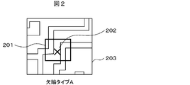
- An enlarged image 203 of the danger point 102 is shown in FIG. 2, and an enlarged image 303 of the danger point 103 is shown in FIG.
- FIG. 2 Although there are actually many parts similar to the circuit shape shown in FIG. 2 in addition to the points indicated by the danger point 102 in the semiconductor chip 101, only one danger point 102 is shown in FIG. 1 for simplicity. The same applies to the danger point 103.
- the 2 is an expected short-circuit defect occurrence area 201 serving as an inspection area, which is a portion where a short circuit of the pattern may occur due to the circuit shape of this part.
- the point 202 is the center coordinate position of the short-circuit defect occurrence predicted area 201, and the point 202 is controlled to be positioned at the center of the short-circuit defect occurrence predicted area 201 that is the inspection visual field.
- Reference numeral 301 in FIG. 3 denotes an expected disconnection defect generation region serving as an inspection region, which is a portion where a pattern disconnection may occur due to the circuit shape of this portion.
- a point 302 is a center coordinate of the expected disconnection defect occurrence area 301, and a point 302 is a point that is controlled to be positioned at the center of the expected disconnection defect occurrence area 301 that is the inspection field of view.
- defect type codes are assigned as defect type C and defect type D.
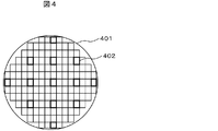
- FIG. 4 is a wafer map schematically showing a wafer to be inspected and a semiconductor chip manufactured thereon.
- a semiconductor chip 402 indicated by a thick black frame is a semiconductor chip to be inspected (hereinafter referred to as an inspection target chip). As shown in FIG. 4, the inspection target chips 402 may be selected selectively, or all the chips may be targeted.
- FIG. 5 is a diagram showing the inspection target chip 501 in which the defect type A has a defect higher than the reference value among the results of the inspection of the inspection target chip 402 shown in FIG. 4, or the inspection target chip 402 shown in FIG. It is an example of the figure which shows the chip
- FIG. 6 is an overall view including an apparatus and a system related to the defect determination system as the present system.
- Defect determination unit 601 design data server 602 for managing design data, wafer SEM inspection by step and repeat, for example, inspection apparatus 603 equipped with SEM such as a defect review SEM apparatus or length measurement SEM apparatus, lithography simulator 605 is connected to the LAN 604.
- the litho simulator 605 is not limited to litho as described later, and is not necessarily required.
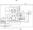
- FIG. 7 shows the configuration of an inspection apparatus 603 equipped with an SEM.
- An inspection apparatus 603 including an SEM includes an SEM apparatus main body 70, an overall control system 719, a data input / output I / F 725, an image processing system 727, a secondary storage device 717, and a computer 718.
- the SEM apparatus main body 70 includes the following electron optical system and detection system.
- Reference numeral 701 denotes an electron source that emits an electron beam 700. After the emitted electron beam 700 passes through the electron lenses 702 and 703, astigmatism and misalignment are corrected by the electron beam axis adjuster 704.
- Reference numerals 705 and 706 denote two-stage deflectors that deflect the electron beam 700 and scan the wafer 708. The electron beam 700 is converged by the objective lens 707 and focused on the imaging target area 709 of the wafer 708.
- Secondary electrons and reflected electrons detected by the detector 711 are converted into digital signals by the A / D converter 712 and stored in the memory 714.
- An adder circuit 713 is disposed between the A / D converter and the memory. When the electron beam 700 is raster-scanned on the imaging target region 709, the adder circuit 713 reduces shot noise by calculating an addition average (frame addition) of detection signals obtained at the same beam irradiation position. And an image signal having a high S / N can be obtained.
- Reference numeral 715 denotes an image processing unit, which detects a defect using an image stored in the memory 714.
- Reference numeral 727 denotes an image signal processing system.
- Reference numeral 716 denotes an XY stage that moves the wafer 708 and enables imaging of an arbitrary position on the wafer 708.
- the secondary storage device 717 can store an image stored in the memory 714.
- the abnormal portion of the inspection target region 709 obtained by image processing and the appearance characteristics of the abnormal portion can also be stored in the memory 714.
- the computer 718 includes an arithmetic device, a storage device, a display device, and an input device, and can display an image stored in the secondary storage device 717 or the memory 714. Also, the user can control and set the operations of the SEM apparatus main body 70, the image processing system 727, and the overall control system 719 shown in FIG.
- the overall control system 719 includes a current amount control unit 720 of the electron source 701 of the electron beam 700, a deflection control unit 721 that controls the deflectors 705 and 706, and an electron lens control unit 722 that controls the electron lenses 702, 703, 704, and 707. , A stage control unit 723 for controlling the visual field movement due to the movement of the XY stage 715, and a sequence control unit 724 for controlling the entire inspection sequence.
- the data input / output I / F 725 receives the inspection point coordinate data from the LAN 604 and stores it in a memory (not shown) in the sequence control unit 724.
- the inspection apparatus 603 moves the XY stage 715 by the stage control unit 723 based on the inspection coordinate data stored in the memory (not shown) in the sequence control unit 724, captures the electron beam image after the movement, and displays the captured image. By processing with the image processing unit 715, the presence or absence of a defect at the inspection coordinate point is determined.
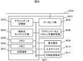
- FIG. 8 is a configuration diagram of the defect determination unit 601.
- Data exchange with the LAN 604 is performed by the data I / F unit 802, and internal data transmission is performed by the bus 801.
- a design data storage unit 803, an inspection point sampling unit 804, a CPU 805, a memory 806, a storage medium 807 such as a hard disk or a non-volatile memory, and a design data upper pattern position specifying unit 808 are connected to the bus 801 and displayed externally.
- An input device 810 such as a terminal 809 and a keyboard for numerical data input and data designation is connected.
- an external storage medium 811 such as a hard disk, a nonvolatile memory, or a CD-ROM may be connected to the outside.
- FIG. 9 is a schematic flow of defect determination.
- a risk point to be an inspection location on the design data is input from the design data server 602 to the design data pattern position specifying unit 808 from the data I / F unit 802 via the LAN 604 (S901).
- the danger point information is composed of the position coordinates of the danger point on the wafer and the expected defect type code.
- the risk point information is input from the lithography simulator 605 as a result of lithography simulation using design data, such as lithography risk point simulation.
- the risk point information by simulation is not limited to litho, and any information can be used as long as the risk point position coordinates and the defect type code can be obtained by simulation.
- a plurality of or all existing positions may be searched, and the position coordinates searched for each defect type may be used as the risk point information together with the defect type code.
- the information is transmitted from the litho simulator 605 shown in FIG. 6 to the defect determination unit 601 via the LAN 604.
- the transmitted risk point information is stored in the design data storage unit 803 via the data I / F unit 802 in association with the defect type.
- the design data of the target inspection layer is transferred from the design data server 602 shown in FIG. 6 to the defect determination unit 601 via the LAN 604.
- the transferred design data is stored in the design data storage unit 803 via the data I / F unit 802.
- the manual dangerous point indication on the design data is an image of the design data shown on the display terminal 809, and the input device 810 inputs the dangerous point position and the defect type code on the design data.
- the design data pattern position specifying unit 808 uses the input design data as a template to search for a plurality or all of the corresponding positions on the design data stored in the design data storage unit 803, and designs it as risk point information together with the defect type code.
- the data is stored in the data storage unit 803.
- the inspection target chip is designated (S902).
- the inspection target chip is a chip that is actually inspected among the chips formed on the wafer as indicated by 402 in FIG. This designation may be performed by the defect determination apparatus 601 or the inspection apparatus 603.
- the inspection point sampling unit 804 samples a predetermined number of points (here, N) for each defect type from the risk point information stored in the design data storage unit 803 as an inspection point. As a result, inspection points for each defect type for one chip are determined, and the inspection points sampling unit 804 develops the inspection points to all inspection target chips (S903). The expansion to all the points of the chip is performed on the apparatus where the inspection target chip is designated, that is, the defect determination unit 601 or the inspection apparatus 603. When the defect determination device 601 develops inspection points to all chips, sampled risk point information, that is, inspection point information, is temporarily stored in the storage medium 807, and the stored inspection point information is stored in the data I / F unit. The data is transferred from 802 to the inspection device 603 via the LAN 604.
- N predetermined number of points
- the inspection device 603 stores the transmitted inspection point information in a memory (not shown) in the sequence control unit 724 via the data input / output I / F 725.
- sampled risk point information for each chip that is, inspection point information
- the inspection point information is developed using the inspection target chip information and stored in a memory (not shown) in the sequence control unit 724.
- CPU 805 controls the entire defect determination unit 601.
- the ratio of the defect to the sampling point number N is calculated for each chip and for each defect type, and the sampling point N, the defect ratio, and the confidence interval calculated therefrom are compared with a preset reference (S905).
- a chip having a defect type exceeding the reference is specified and displayed on the display terminal 809 as a wafer map, for example, as shown in FIG. 5 (S906).
- the defect sampling number N is 100, 200, 300.
- the defect sampling number N is 100, 200, 300.
- the error is about 6%
- a true ratio exists with a reliability of 95% within a range of 10 ⁇ 6%.
- This interval of P ⁇ e is called a confidence interval.
- the obtained defect ratio is compared with the reference value TH. If TH ⁇ Pe, the defect ratio exceeds the reference value with 95% reliability.
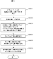
- FIG. 11 Detailed procedure of the inspection is shown using FIG. 11 to FIG. The detailed flow in FIG. 11 corresponds to S904 and subsequent steps in FIG.
- a reference value (threshold value) for the defect ratio obtained by the inspection is set prior to the inspection.
- the sampled inspection points are inspected (corresponding to S1101; S904).
- a confidence interval of the defect ratio is calculated for each chip and each defect type (S1102).
- FIG. 12 shows an example of a GUI 1200 that performs a graph display 1210 in which a defect ratio of defect types A, B, C, D, and E in a certain chip in the middle of an inspection is represented by a bar graph 1201 and its confidence interval is represented by a bar chart 1202.
- the reference value 1203 for the defects C and D is within the confidence intervals 12021 and 12022, and the defect determination cannot be performed with a predetermined reliability ⁇ .
- the defect class for each defect class divided for each chip is examined, and a predetermined sampling number N is sampled again from the uninspected points of the defect class divided for each corresponding chip (S1104). Is executed (S1105).
- steps S1103 to S1106 are executed. Also, on the GUI screen 1200, a button 1204 for continuing the inspection and a button 1205 for continuing the inspection are displayed, and when the operator clicks any button, the sampling is executed again or the inspection is performed. You can choose to finish and go to the next step.
- the sampling number N in the case of sampling again does not need to be the same as the first sampling number.
- a confidence interval of the defect occurrence ratio of the defect class divided by the corresponding chip is calculated (S1106; S1102 to S1107 correspond to S905), and the confidence interval and the reference value are compared again ( S1103).
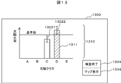
- the process proceeds to output of the defect determination result (S1107; corresponding to S906), displays a graph 1310 on the GUI screen 1310, and exceeds the reference value (in the example of FIG.
- the defect class D: 1311) is displayed and the inspection end display 13041 is turned on.
- a map display button 13042 is clicked on the GUI screen 1300, the screen is switched to a GUI screen 1400 as shown in FIG.
- the inspected chip 1411 is distinguished from the uninspected chip 1412 and displayed on the wafer map 1410.
- information 1413 on classification according to the density of detected defects and information 1414 on the defect type of the displayed defect are displayed.
- FIG. 14 shows a defect density state for each chip related to the defect type A.
- the defect density state for each chip related to the defect type B is displayed on the wafer map 1410.
- an enlarged image 1420 of the clicked chip is displayed.
- the screen is switched to the GUI screen 1300 of the graph display of FIG.
- S1104 and subsequent steps are repeated until the defect can be determined.
- the result output of S1107 is not limited to the wafer map, and any form may be used as long as the defect class exceeding the reference value and its chip are known.
- FIG. 15 shows a processing flow of a method for determining the upper limit of the number of inspection points or the inspection time and deciding whether to continue or interrupt the inspection based on the judgment of the operator.
- 15 is based on the premise that the inspection is cyclically performed for each chip and for each defect type. For example, if there are chips No. 1 to M and defect types A to C, (m, n) is assumed to indicate the m-th defect type n of the chip, and a specific example is to inspect cyclically. Indicates (1, A) (1, B) (1, C) (2, A) ... (M, B) (M, C) (1, A) (1, B) ..., chip, defect type This means that the same combination is not inspected until the combination is completed.
- one combination inspection for example, (1, A) inspection
- the next inspection for example, the inspection of (1, B)
- the reference value (threshold value) for the defect ratio obtained by the inspection and the maximum number of inspection points for the defect type for each chip are set as specified values.
- the order of the inspection follows the above example, and (1, A) (1, B) (1, C) (2, A)... (M, B) (M, C) (1, A) (1 , B)... Is created and performed in this order.
- step S1501 (1, A) is inspected, and in step S1502, it is determined whether the (1, A) inspected score has reached the specified value. If it has reached, the process proceeds to S1505 (1A) is excluded from the inspection list, and if there are other inspection points (S1506), the process returns to S1501 to inspect the next inspection point (1, B). If the number of points that have been inspected in S1502 has not reached the specified value, the process advances to S1503 to calculate a confidence interval of the defect occurrence ratio (1, A), and compares the confidence interval with a reference value (S1504). If there is a reference value in the confidence interval, the process returns to S1501 to inspect the next point (1, B). If there is no reference value in the confidence interval, defect determination is possible, so (1, A) is excluded from the inspection list (S1505), and if there are other inspection points (S1506), the process returns to S1501 for the next inspection. Check point (1, B).
- the process proceeds to S1507. If there is no reference value in the confidence interval for all chips and defect types, the process proceeds to S1509 and the inspection result is output. If there is a reference value in the confidence interval, the operator is inquired whether to continue the inspection (S1508). If the inspection continues, the inspection point of the combination of the chip and the defect type having the reference value in the confidence interval is resampled. The inspection circulation list in this combination is recreated, and the process returns to S1501.
- the process proceeds to defect display S1509. At this time, a combination of a chip and a defect type that cannot be determined yet remains, but those that do not complete the defect determination are displayed with different colors.
- the description has been made in the order from (1, A), but the inspection proceeds according to a list that is cyclically assembled with (1, B) (1, C) (2, A).
- the example of performing the defect determination by comparing the reference value with the confidence interval of the defect ratio has been described, but the comparison by the defect ratio between chips of the same defect class, or between the defect classes in one chip or a plurality of chips. Comparison of defect ratios may be performed.
- An example of the comparison determination result is a comparison of two ratios that give the maximum and minimum values among a plurality of ratios.
- the confidence interval between the two is divided into the case where they do not overlap and the case where they overlap, and if they do not overlap, it can be determined that there is a difference between the mutual ratios, that is, there is a significant difference. It can be determined that there is no difference between them, that is, there is no significant difference. If there is a difference, the chip or defect type with the highest defect rate is displayed on the wafer map. At the time of display, the screen is switched for each defect type, and only the corresponding chip is highlighted and displayed in the format shown in FIG.
- Objective lens 708 Wafer 709 ... Imaging target area 710 ... Reflector 711 ... Detector 712 ... A / D converter 713 ... Adder circuit 714 ... Memory 715 ... Image processing unit 71 6 ... XY stage 717 ... secondary storage device 718 ... computer 719 ... overall control system 720 ... current amount control unit 721 ... deflection control unit 722 ... electronic lens control unit 723 ... stage control unit 724 ... sequence control unit 725 ... data input / output I / F 801 ... Bus 802 ... Data I / F section 803 ... Design data storage section 804 ... Inspection point sampling section 805 ... CPU 806 ... Memory 807 ... Storage medium 808 ... Design data upper pattern position specifying section 809 ... Display terminal 810 ... Input device 811: External storage medium.
Landscapes
- Engineering & Computer Science (AREA)
- Quality & Reliability (AREA)
- Computer Vision & Pattern Recognition (AREA)
- Physics & Mathematics (AREA)
- General Physics & Mathematics (AREA)
- Theoretical Computer Science (AREA)
- Testing Or Measuring Of Semiconductors Or The Like (AREA)
Abstract
ステップ・アンド・リピート式の高解像度SEMを用いて予め定められた危険点を検査し、危険点での欠陥発生頻度を統計的かつ信頼性を持って推定する半導体デバイスの欠陥検査方法及びそのシステムを提供するものであって、デザインデータ上で欠陥タイプ別に検査点を指定し、この指定された検査点の中から予め指定された数の検査点を欠陥タイプ別に選択し、この選択した欠陥タイプ別に予め指定された数の検査点を撮像してこの検査点における欠陥を検出し、欠陥タイプ別に撮像した検査点の数に対する検出した欠陥の数の比である欠陥比率とこの欠陥比率の信頼区間を算出し、この算出した欠陥タイプ別の欠陥比率の信頼区間と予め設定した基準値とを比較し、この基準値を超える欠陥発生比率をもつ欠陥タイプを求める半導体デバイスの欠陥検査方法及びそのシステムとした。
Description
本発明は半導体ウェハの前工程における外観検査に関するものであり、特に予め指定された点を検査し欠陥発生の状況を効率的に評価する半導体デバイスの欠陥検査方法およびそのシステムに関するものである。
半導体デバイスの回路パターンの微細化が進むに従い、その製造方法はより精緻さを増している。これに伴い、生じる欠陥にも変化が見られる。すなわち、従来は塵埃や異物等によるランダムに発生する欠陥が支配的であったのに対し、回路微細の微細化に伴い、配線や素子の配置に相関性のあるデザイン依存性の高い欠陥や、特定の層(レイヤともいう)の形状や層の重なりなどによって生じる欠陥が増加している。これら回路デザイン依存性の高い欠陥はシステマティック欠陥と呼ばれる。例えば、露光工程における光近接効果による転写パターンの短絡、断線や、下地段差起因のパターン形状変動による抵抗異常、特定領域のゲート酸化膜のエッチング不足によるコンタクトホール導通不良などである。
これらのシステマティック欠陥が発生しないよう回路デザインは設計されるが、なおプロセスマージンの少ない部分が危険点(プロセスの変動に対して欠陥が出やすい場所)として残る。危険点は製造前にシミュレーションなどにより予見できる点のほか、製造後に経験的にためられた知見として定められる点である場合もある。これらの危険点で発生するシステマティック欠陥は、製造条件を一部変更したりすることによって、その発生を防止することができる場合が多い。このため、検査装置により検出された欠陥から、危険点で発生した欠陥の有無を判定する機能に対する要求が高まっている。
システマティック欠陥を観察する方法として、特許文献1には、外観検査で得られた欠陥部位に相当する検査画像とデザインデータを画像化したものを比較した上で、該当するデザインデータ上の回路部位を特定し、回路形状ごとに分類することで頻度高く出現する回路形状を検出する方法が開示されている。
また、特許文献2には、外観検査装置により検出した欠陥の幾何学的な特徴とデザインデータを照合して危険点を判定することが記載されている。
システマティック欠陥は微細な回路デザインの位置関係に依存して発生するものである。回路デザインの設計段階でシステマティック欠陥が発生しないよう回路設計がなされるが、ウェハを製造した段階でこれを検証するために、光学式外観検査あるいはSEM式外観検査装置でウェハの部分あるいは全面を走査し検査が行われる。
しかし、引用文献1に記載されている方法では、検査画像の分解能が高くなくデザインデータとの正確な比較ができない、また検査装置の座標系とデザインデータの座標系の合わせの誤差や、検出した欠陥座標が欠陥検出アルゴリズムに依存するため(例えば欠陥画像と参照画像の差分から得られた欠陥信号の重心位置など)着目したいシステマティック欠陥の位置座標とずれるなどの理由により検出欠陥位置に対応する回路形状を正確に特定できず、よって危険点で発生した欠陥の頻度を正確に評価できないという課題があった。
また、特許文献2に記載されている方法では、外観検査装置により検出した欠陥の幾何学的な特徴とデザインデータを照合して危険点を判定するために、着目したいシステマティック欠陥の位置座標とずれるなどの理由により検出欠陥位置に対応する回路形状を正確に特定できず、危険点で発生した欠陥の頻度を正確に評価できないという課題があった。
上記課題に鑑み本発明の目的は、ステップ・アンド・リピート式の高解像度SEMを用いて予め定められた危険点を検査し、危険点での欠陥発生頻度を統計的かつ信頼性を持って推定する半導体デバイスの欠陥検査方法及びそのシステムを提供することにある。
上記した課題を解決するために、本発明では、半導体デバイスの欠陥検査方法において、デザインデータ上で欠陥タイプ別に検査点を指定し、この指定された検査点の中から予め指定された数の検査点を欠陥タイプ別に選択し、この選択した欠陥タイプ別に予め指定された数の検査点を撮像してこの検査点における欠陥を検出し、欠陥タイプ別に撮像した検査点の数に対する検出した欠陥の数の比である欠陥比率とこの欠陥比率の信頼区間を算出し、この算出した欠陥タイプ別の欠陥比率の信頼区間と予め設定した基準値とを比較し、この基準値を超える欠陥発生比率をもつ欠陥タイプを求めるようにした。
また、上記した課題を解決するために、本発明では、半導体デバイスの欠陥検査方法において、デザインデータ上で欠陥タイプ別に検査点を指定し、この指定された検査点の中から予め指定された数の検査点を欠陥タイプ別に選択し、この選択した欠陥タイプ別に予め指定された数の検査点を撮像してこの検査点の画像からこの検査点における欠陥を検出し、欠陥タイプ別に撮像した検査点の数に対する検出した欠陥の数の比である比率を計算し、この算出した欠陥タイプ別の欠陥比率の有意差を計算し、この計算した結果から欠陥の比率に有意差が有る欠陥タイプを求めるようにした。
また、上記した課題を解決するために、本発明では、半導体デバイスの欠陥検査システムを、デザインデータ上で欠陥タイプ別に検査点を指定する検査点指定手段と、この検査点指定手段で指定された検査点の中から予め指定された数の検査点を欠陥タイプ別に入力する入力手段と、この入力手段で入力した欠陥タイプ別に予め指定された数の検査点を撮像する撮像手段と、この撮像手段で撮像して得た検査点の画像を処理して欠陥を検出する画像処理手段と、撮像手段で撮像した欠陥タイプ別の検査点の数に対する画像処理手段で検出した欠陥タイプ別の欠陥の数の比率である欠陥比率と欠陥タイプ別の欠陥比率の信頼区間を計算する演算手段と、この演算手段で算出した欠陥タイプ別の欠陥比率の信頼区間と予め設定した基準値とを比較する比較手段と、基準値を超える欠陥比率をもつ欠陥タイプを求める欠陥タイプ抽出手段と、この欠陥タイプ抽出手段で求めた欠陥タイプに関する情報を出力する出力手段とを備えて構成した。
また、上記した課題を解決するために、本発明では、半導体デバイスの欠陥検査システムを、デザインデータ上で欠陥タイプ別に検査点を指定する検査点指定手段と、この検査点指定手段で指定された検査点の中から予め指定された数の検査点を欠陥タイプ別に入力する入力手段と、この入力手段で入力した欠陥タイプ別に予め指定された数の検査点を撮像する撮像手段と、この撮像手段で撮像して得た検査点の画像を処理して欠陥を検出する画像処理手段と、撮像手段で撮像した欠陥タイプ別の検査点の数に対する画像処理手段で検出した欠陥タイプ別の欠陥の数の比率である欠陥比率と該欠陥タイプ別の欠陥比率の信頼区間を計算する演算手段と、この演算手段で算出した欠陥タイプ別の欠陥比率の有意差を計算する有意差算出手段と、この有意差計算手段で計算した結果から欠陥比率に有意差が有る欠陥タイプを求める欠陥タイプ抽出手段と、この欠陥タイプ抽出手段で求めた欠陥タイプに関する情報を出力する出力手段とを備えて構成した。
本発明によれば、半導体デバイス製造の前工程において半導体ウェハ上に形成された回路パターンの危険点に発生した欠陥の頻度を信頼性高く効率的に評価できるので、製造条件の変更などの対策を迅速に行うことが可能となる。
以下に、図面を用いて本発明の実施例を説明する。
本実施例で対象とする欠陥の例を図1、図2、図3で、検査の様子を図4、図5に示す。図1の101は半導体ウェハ上に形成されたチップ(以下、半導体チップと記す)である。半導体チップ101の内部には多数の回路パターンが形成されているが、図1に示した構成では、それらの回路パターンの表示を省略している。図1の半導体チップ101の102及び103はプロセスの変動に対して欠陥が出やすい場所、すなわち危険点である。危険点102の拡大画像203を図2に、危険点103の拡大画像303を図3に示す。図2に示す回路形状と同様の部位は半導体チップ101内の危険点102に示す点以外にも実際は多数あるが、図1では簡単のため危険点102の1点のみを示してある。危険点103に関しても同様である。
図2の201は検査領域となる短絡欠陥発生予想領域であり、この部分の回路形状からパターンの短絡が発生する可能性のある部位である。点202は短絡欠陥発生予想領域201の中心座標位置であり、点202は検査視野である短絡欠陥発生予想領域201の中心に位置するよう制御される。図3の301は検査領域となる断線欠陥発生予想領域であり、この部分の回路形状からパターンの断線が発生する可能性のある部位である。点302は断線欠陥発生予想領域301の中心座標であり、点302は検査視野である断線欠陥発生予想領域301の中心に位置するよう制御される点である。
図2及び図3に示した発生が予想される欠陥は種類が異なることから、図2に示した検査領域である短絡欠陥発生予想領域201で発生が予想される欠陥を欠陥タイプA、図3に示した検査領域である断線欠陥発生予想領域301で発生が予想される欠陥を欠陥タイプBと呼ぶことにする。図には示さないがこのほかにも発生が予想される欠陥種があれば欠陥タイプコードを欠陥タイプC,欠陥タイプDというように割り当てる。
図4の401は検査対象となるウェハとその上に製造される半導体チップを模式的に示したウェハマップである。太い黒枠で示した半導体チップ402は検査対象の半導体チップ(以下、検査対象チップと記す)である。図4に示したように検査対象チップ402は選択的に選んでも良いし、全数を対象としても良い。
図5は図4に示した検査対象チップ402を検査した結果のうち欠陥タイプAについて基準値以上の欠陥発生があった検査対象チップ501を示す図、あるいは図4に示した検査対象チップ402を検査した結果のうち欠陥タイプAが他の欠陥タイプより相対的に発生頻度が高かった検査対象チップ501を示す図の例であり、本実施例の出力表示の一形態を示す図である。
以下、図6から図14を用いて基準比率の算出について説明する。 図6は本システムである欠陥判定システムと関連する装置およびシステムを含めた全体図である。欠陥判定ユニット601、デザインデータを管理するデザインデータサーバ602、ウェハのSEM検査をステップ・アンド・リピートで行う例えばディフェクトレビューSEM装置、あるいは測長SEM装置などのSEMを備えた検査装置603、リソシミュレータ605がLAN604に接続されている。リソシミュレータ605は後述のようにリソに限定されるものではなく、また必ずしも必要なものでもない。
図7にSEMを備えた検査装置603の構成を示す。SEMを備えた検査装置603は、SEM装置本体70、全体制御系719、データ入出力I/F725、画像処理系727、二次記憶装置717及びコンピュータ718を備えて構成されている。
SEM装置本体70の内部には、以下の電子光学系及び検出系を備える。701は電子源であり、電子ビーム700を射出する。射出された電子ビーム700は電子レンズ702、703を通過した後、電子ビーム軸調整器704により非点収差やアライメントずれを補正される。705と706は2段の偏向器であり電子ビーム700を偏向し、ウェハ708上を走査させる。電子ビーム700は対物レンズ707により収束されてウェハ708の撮像対象領域709で焦点を結ぶ。撮像対象領域709からはこの結果、2次電子と反射電子が放出され、2次電子および反射電子は一次電子ビーム通過穴710’を有する反射板710に衝突し、そこで発生した二次電子が電子検出器711により検出される。
検出器711で検出された2次電子および反射電子はA/Dコンバータ712でデジタル信号に変換され、メモリ714に格納される。なお、A/Dコンバータとメモリとの間には加算回路713が配置されている。加算回路713は,電子ビーム700を撮像対象領域709上でラスタ走査する場合に,同一のビーム照射位置で得られた検出信号の加算平均(フレーム加算)を算出することで,ショットノイズを小さくすることを可能になり、S/Nの高い画像信号を得ることができる。715は画像処理ユニットであり、メモリ714に格納された画像を用いて欠陥の検出が行われる。727は画像信号処理系を表す。716はXYステージであり、ウェハ708を移動させ、ウェハ708の任意の位置の画像撮像を可能にしている。
二次記憶装置717は、メモリ714に格納された画像を記憶することが可能である。また,画像処理により得られた検査対象領域709の異常部や,異常部の外観特徴もメモリ714に格納することができる。コンピュータ718は、演算装置、記憶装置、表示装置、入力装置を備えるものであるとともに、二次記憶装置717、あるいはメモリ714に格納された画像を表示することができる。また、ユーザは端末718に入力することにより、図1に示すSEM装置本体70、画像処理系727、全体制御系719の動作の制御、及び設定を行うことができる。
全体制御系719は、電子ビーム700の電子源701の電流量制御ユニット720,偏向器705と706を制御する偏向制御ユニット721,電子レンズ702と703と704と707を制御する電子レンズ制御ユニット722,XYステージ715の移動による視野移動を制御するステージ制御ユニット723,検査シーケンス全体を制御するシーケンス制御ユニット724を備えている。データ入出力I/F725は、LAN604から検査点座標データを受け取り、724のシーケンス制御ユニット内のメモリ(図示せず)に格納する。
検査装置603は724のシーケンス制御ユニット内のメモリ(図示せず)に格納された検査座標データに基づきステージ制御ユニット723によりXYステージ715を移動し、移動後電子線画像を撮像し、撮像画像を画像処理ユニット715で処理することにより検査座標点における欠陥の有無を判定する。
図8は欠陥判定ユニット601の構成図である。LAN604とのデータの授受はデータI/F部802により行われ、内部のデータ伝送はバス801により行われる。バス801には、デザインデータ記憶部803、検査点サンプリング部804、CPU805、メモリ806、ハードディスクあるいは不揮発性メモリ等の記憶媒体807、デザインデータ上パターン位置特定部808が接続されており、外部に表示端末809、キーボードなど数値データ入力や、データの指定を目的とした入力デバイス810が接続されている。また外部にはハードディスク、不揮発性メモリ、CD-ROMなどの外部記憶媒体811が接続されていてもよい。
図9は欠陥判定の概略フローである。まずデザインデータ上で検査箇所となる危険点をデザインデータサーバ602からLAN604を介してデータI/F部802からデザインデータ上パターン位置特定部808に入力する(S901)。危険点情報は危険点のウェハ上の位置座標と、予想される欠陥タイプコードから構成される。危険点情報は、例えばリソの危険点シミュレーションのようにデザインデータを用いたリソシミュレーションの結果をリソシミュレータ605から入力する。シミュレーションによる危険点情報はリソに限定されるものではなく、シミュレーションにより危険点位置座標と欠陥タイプコードが得られるものであればなんでも良い。あるいは、デザインデータ上で危険点を欠陥タイプ別にマニュアル入力し、欠陥タイプ別に登録されたデザインデータの形状をテンプレートとして、1チップ分あるいは検査に必要な領域分のデザインデータから同じ形状のデザインデータの存在する位置を複数あるいは全て探し、欠陥タイプ別に探した位置座標を欠陥タイプコードとともに危険点情報としても良い。
リソシミュレーションの結果を危険点情報とする場合は、図6で示したリソシミュレータ605からLAN604を介して欠陥判定ユニット601に情報を送信する。送信された危険点情報はデータI/F部802を介してデザインデータ記憶部803に欠陥タイプと対応をつけて記憶される。デザインデータ上で危険点を欠陥タイプ別にマニュアル入力する場合は、対象とする検査レイヤのデザインデータを図6で示したデザインデータサーバ602からLAN604を介して欠陥判定ユニット601に転送する。転送されたデザインデータはデータI/F部802を介してデザインデータ記憶部803に記憶される。マニュアルによるデザインデータ上の危険点指示は、デザインデータを画像化したものを表示端末809に示し、入力デバイス810によりデザインデータ上の危険点位置および欠陥タイプコードを入力する。入力されたデザインデータをテンプレートとして、デザインデータ上パターン位置特定部808によりデザインデータ記憶部803に記憶されているデザインデータ上の対応する位置を複数あるいは全て探し、欠陥タイプコードとともに危険点情報としてデザインデータ記憶部803に記憶する。
次に検査対象チップを指定する(S902)。検査対象チップとは図4の402で示したようにウェハ上で作成されたチップのうち実際に検査を行うチップのことである。この指定は欠陥判定装置601で行ってもよいし、検査装置603で行っても良い。
次にデザインデータ記憶部803に記憶されている危険点情報から欠陥タイプ別に予め定められた点数(ここではNとする)を検査点として検査点サンプリング部804によりサンプリングする。これにより1チップ分の欠陥タイプ別の検査点が定まるので、これを検査点サンプリング部804で検査対象チップ全点に展開する(S903)。チップ全点への展開は、検査対象チップの指定が行われた装置上、すなわち欠陥判定ユニット601あるいは検査装置603で行われる。検査点のチップ全点への展開が欠陥判定装置601で行われる場合は、サンプリングされた危険点情報すなわち検査点情報を記憶媒体807に一時記憶し、記憶した検査点情報をデータI/F部802からLAN604を介して、検査装置603に転送する。
検査装置603では送られてきた検査点情報をデータ入出力I/F725を介して、724のシーケンス制御ユニット内のメモリ(図示せず)に格納する。検査点のチップ全点への展開が検査装置603で行われる場合は、1チップ分の欠陥タイプ別のサンプリングされた危険点情報すなわち検査点情報を欠陥判定装置601から受け取り、コンピュータ718から入力された検査対象チップ情報を用いて検査点情報を展開し、724のシーケンス制御ユニット内のメモリ(図示せず)に格納する。 CPU805は、欠陥判定ユニット601全体の制御を行う。
次にシーケンス制御ユニット724内のメモリ(図示せず)に格納された検査点情報に従い検査を実行し、検査点に対する検査結果を得る(S904)。
検査結果は、チップごと、欠陥タイプごとにサンプリング点数Nに対する欠陥の比率を計算し、後述するサンプリング点数N、欠陥比率、およびそれから計算される信頼区間と、予め設定した基準と比較する(S905)。比較の結果、基準を超える欠陥タイプのあるチップを特定し、例えば図5に示したようにウェハマップとして表示端末809に表示する(S906)。
図10に図11、図12、図13で使用する信頼区間の考え方を示す。N点の検査点を検査し、その内の欠陥と判定された比率である欠陥比率をPとすれば、推定される分散Sは、S=sqrt( P*(1-P)/N )( sqrt(X)はXの平方根を表す )である。信頼度α=95%でPが分布する範囲は標準正規分布表より[ P-1.96*S、P+1.96*S ]だから、誤差e(母比率の推定誤差)は e= 1.96*S = 1.96*sqrt( P*(1-P)/N )である。図10は横軸に欠陥比率P、縦軸に誤差eを取り、欠陥サンプリング数Nが100,200,300のときの欠陥比率と誤差eの推移を示したものである。例えば100点検査し10点欠陥であった場合(欠陥比率0.1=10%)、誤差は約6%であり10±6%の範囲に95%の信頼度で真の比率は存在する。このP±eの区間を信頼区間と呼ぶ。信頼度α=95%で得られたeを用いた場合、得られた欠陥比率と基準値THを比較し、TH<P-eであれば信頼度95%で欠陥比率は基準値を上回っており、P+e<THであれば信頼度95%で欠陥比率は基準値を下回っていると判断できる。また信頼度95%で判断が求められる場合、P-e≦TH≦P+eのときPは基準値THを上回るか、下回るか判断できない、すなわち欠陥判定ができない。信頼度αは任意に設定できる数字であり、それに応じて標準正規分布表より以上を再計算すればよい。
図11乃至図14を用いて検査の詳細な手順を示す。図11の詳細フローは図9のS904以降に対応するものである。検査に先立ち検査で得られる欠陥比率に対する基準値(しきい値)を設定しておく。まずサンプリングされた検査点を検査し(S1101;S904に対応)、検査終了後、チップ別、欠陥タイプ別に欠陥比率の信頼区間を計算する(S1102)。次にチップ別に分けられた欠陥タイプ別に信頼区間内に基準値があるか評価する(S1103)。
図12は、検査の途中におけるあるチップにおける欠陥タイプA,B,C,D,Eの欠陥比率を棒グラフ1201で、その信頼区間をバーチャート1202で示したグラフ表示1210を行うGUI1200の一例を示す図である。この例では欠陥C,Dについて基準値1203が信頼区間12021及び12022の内にあり、予め定められた信頼度αでの欠陥判定ができない。このようにチップ別に分けられた欠陥クラスごとに欠陥判定のできないものを調べ、該当するチップ別に分けられた欠陥クラスの未検査点から予め定められたサンプリング数Nを再度サンプリングし(S1104)、検査を実行する(S1105)。
検査を実行した結果、再度サンプリングを実行する必要が有るか否かを判断し、再度サンプリングが必要と判断された場合には、S1103からS1106までを実行する。また、GUI画面1200上にも、検査続行要のボタン1204と検査続行否のボタン1205とが表示されており、オペレータが何れかのボタンをクリックすることにより再度サンプリングを実行するか、又は検査を終了して次のステップに進むかを選択することができる。再度サンプリングする場合のサンプリング数Nは1回目のサンプリング数と同じである必要はない。再検査の結果、前記該当するチップ別に分けられた欠陥クラスの欠陥発生比率の信頼区間を計算し(S1106;以上、S1102からS1107までがS905に対応)、再度信頼区間と基準値を比較する(S1103)。
この結果、図13のGUI画面1310に示すように、図12のGUI画面1200上に例示した該当欠陥クラスC及びDにおいて信頼区間13021及び13022が何れも基準値を含まない状態になり信頼度αでの欠陥判定ができるようになれば、欠陥判定結果の出力(S1107;S906に対応)に進み、GUI画面1310上でグラフ1310を表示して基準値を超える欠陥タイプ(図13の例では、欠陥クラスD:1311)を表示するとともに検査終了の表示13041を点灯させる。このGUI画面1300上でマップ表示ボタン13042をクリックすると、図14に示すようなGUI画面1400に切り替わる。
GUI画面1400上では、検査したチップ1411を未検査のチップ1412と区別してウェハマップ1410上に表示する。また、検査したチップ1411については、検出された欠陥の密度に応じたクラス分けの情報1413と、表示されている欠陥の欠陥種の情報1414とが表示される。
図14は、欠陥種Aに関する各チップごとの欠陥密度の状態を示している。カーソル1401を欠陥種Bの位置に移動させてクリックするとウェハマップ1410上に欠陥種Bに関する各チップごとの欠陥密度の状態が表示される。一方、カーソル1401をウェハマップ1410上に表示されている何れかのチップ上に移動させてクリックすると、クリックされたチップの拡大画像1420が表示される。また、カーソル1401をグラフ表示ボタン1432の上に移動させてクリックすると、図13のグラフ表示のGUI画面1300に切り替わる。一方、まだ欠陥判定ができない場合は、S1104以降を欠陥判定が可能になるまで繰返す。
S1107の結果出力はウェハマップに限られるものではなく、基準値を超えた欠陥クラスとそのチップが分かればいかなる形態でも構わない。
図11の処理フローでは欠陥判定が可能になるまで処理を繰返すため、検査点数や検査時間を予測できない。図15は検査点数あるいは検査時間の上限を定め、作業者の判断のもと検査の続行、中断を決める方法の処理フローを示すものである。
図15に示す検査の処理フローでは、検査はチップごと、欠陥タイプごとに循環的に行われることを前提にしている。例えばチップは1番からM番、欠陥タイプはAからCまであるとすれば、(m、n)をチップm番目の欠陥タイプnを示すものとして、循環的に検査するとは具体的な一例としては(1、A)(1、B)(1、C)(2、A)…(M,B)(M,C)(1、A)(1、B)…を指し、チップ、欠陥タイプの組み合わせが一巡しないうちは同一の組み合わせの検査は行わないことを指す。
図15の検査の処理フローにおいて、S1501の検査では一つの組み合わせの検査(例えば(1、A)の検査)を行い、その後S1502に移行する。またS1504,S1506、S1510からS1501に戻ってきたときには、巡回的に定められた次の検査(例えば(1、B)の検査)を行うこととする。検査に先立ち検査で得られる欠陥比率に対する基準値(しきい値)、およびチップごとの欠陥タイプに対する検査点数の最大数を規定値として設定しておく。以下、検査の順番は上記の例にならい、(1、A)(1、B)(1、C)(2、A)…(M,B)(M,C)(1、A)(1、B)…という巡回リストが作成され、この順で行われることとして説明する。
S1501で(1、A)の検査を行い、S1502で(1、A)の検査実施済み点数が規定値に達したか判定する。達していればS1505に進み(1、A)を検査リストから除外し、他の検査点がまだあれば(S1506)S1501に戻り次の検査点(1、B)を検査する。S1502で検査実施済み点数が規定値に達しっていない場合は、S1503に進み(1、A)の欠陥発生比率の信頼区間を算出し、信頼区間と基準値を比較する(S1504)。信頼区間に基準値があればS1501に戻り次の点(1、B)を検査する。信頼区間に基準値がなければ欠陥判定が可能な状態であるので、(1、A)を検査リストから除外し(S1505)、他の検査点がまだあれば(S1506)S1501に戻り次の検査点(1、B)を検査する。
このようにして全ての検査対象点が検査リストから除かれるとS1507に移行し、全てのチップ、欠陥タイプにおいて信頼区間に基準値がなければS1509に移行し検査結果を出力する。信頼区間に基準値がある場合は、検査を続行するか操作者に問い合わせ(S1508)、検査続行の場合は信頼区間に基準値があるチップと欠陥タイプの組み合わせの検査点の再サンプリングを行い、この組み合わせでの検査の巡回リストを作り直し、S1501に戻る。
S1508で検査が中断された場合には欠陥表示S1509に進む。このときまだ欠陥判定ができないチップと欠陥タイプの組み合わせが残るが、欠陥判定が完了しないものについては色を変えて表示するなどする。以上、(1、A)からの順番で説明したが、以降(1、B)(1、C)(2,A)と循環的に組まれたリストに従って検査が進む。
以上、基準値と欠陥比率の信頼区間との比較で欠陥判定を行う例について説明したが、同一欠陥クラスのチップ間の欠陥比率での比較、あるいは一チップ内あるいは複数チップ内の欠陥クラス間での欠陥比率の比較を行ってもよい。
比較の判定結果の一例としては、複数の比率のうち最大と最小を与える二つの比率の比較が考えられる。この場合、両者の信頼区間が重ならない場合と、重なる場合に分けられ、重ならない場合は相互の比率の間に相違が見られる、すなわち有意差があると判断でき、重なる場合は相互の比率の間に相違が見られない、すなわち有意差がないと判断できる。相違が見られる場合、最大の欠陥比率を有するチップあるいは欠陥タイプをウェハマップ上に表示する。表示に際しては欠陥タイプ別に画面を切り替えて図4のような形式で該当するチップのみを強調して表示する。
以上述べた方法によれば半導体前工程において危険点に発生した欠陥の頻度を信頼性高く効率的に評価できるので、製造条件の変更などの対策を迅速に行うことが可能となる。
101…チップ 102…検査点 103…検査点 201…検査視野 202…検査視野中心座標 203…検査点拡大像 301…検査視野 302…検査視野中心座標 303…検査点拡大像 401…ウェハマップ 402…検査対象チップ 501…欠陥タイプA発生チップ 601…欠陥判定ユニット 602…デザインデータサーバ 603…検査装置 604…LAN 605…リソシミュレータ 70…SEM装置本体 700…電子線 701…電子銃 702、703…電子レンズ 704…電子ビーム軸調整器 705,706…偏向器 707…対物レンズ 708…ウェハ 709…撮像対象領域 710…反射板 711…検出器 712…A/Dコンバータ 713…加算回路 714…メモリ 715…画像処理ユニット 716…XYステージ 717…二次記憶装置 718…コンピュータ 719…全体制御系 720…電流量制御ユニット 721…偏向制御ユニット 722…電子レンズ制御ユニット 723…ステージ制御ユニット 724…シーケンス制御ユニット 725…データ入出力I/F 801…バス 802…データI/F部 803…デザインデータ記憶部 804…検査点サンプリング部 805…CPU 806…メモリ 807…記憶媒体 808…デザインデータ上パターン位置特定部 809…表示端末 810…入力デバイス
811…外部記憶媒体。
811…外部記憶媒体。
Claims (12)
- デザインデータ上で欠陥タイプ別に検査点を指定し、
該指定された検査点の中から予め指定された数の検査点を欠陥タイプ別に選択し、
該選択した欠陥タイプ別に予め指定された数の検査点を撮像して該検査点における欠陥を検出し、
前記欠陥タイプ別に撮像した検査点の数に対する検出した欠陥の欠陥比率と該欠陥比率の信頼区間を算出し、
該算出した欠陥タイプ別の欠陥比率の信頼区間と予め設定した基準値とを比較し、
該基準値を超える欠陥発生比率をもつ欠陥タイプを求めることを特徴とする半導体デバイスの欠陥検査方法。 - 請求項1記載の半導体デバイスの欠陥検査方法であって、前記算出した欠陥タイプ別の欠陥比率の信頼区間の範囲に前記予め設定した基準値が含まれる場合には、該欠陥比率の信頼区間の範囲に基準値を含む欠陥タイプについて再度検査点を選択し、該再度選択した検査点を撮像して該検査点における欠陥を検出し、該再度選択した検査点を撮像して検出した欠陥の欠陥比率と前記欠陥タイプ別の欠陥比率の信頼区間を計算し、該計算して求めた欠陥タイプ別の欠陥比率の信頼区間を前記予め設定した基準値と比較し、該基準値を超える欠陥発生比率をもつ欠陥タイプを求めることを特徴とする半導体デバイスの欠陥検査方法。
- 請求項1記載の半導体デバイスの欠陥検査方法であって、前記信頼区間と基準値の比較結果を欠陥タイプ別にウェハマップ上に表示することを特徴とする半導体デバイスの欠陥検査方法。
- デザインデータ上で欠陥タイプ別に検査点を指定し、
該指定された検査点の中から予め指定された数の検査点を欠陥タイプ別に選択し、
該選択した欠陥タイプ別に予め指定された数の検査点を撮像して該検査点の画像から該検査点における欠陥を検出し、
前記欠陥タイプ別に撮像した検査点の数に対する検出した欠陥の比率を計算し、
該算出した欠陥タイプ別の欠陥比率の有意差を計算し、
該計算した結果から欠陥の比率に有意差が有る欠陥タイプを求めることを特徴とする半導体デバイスの欠陥検査方法。 - 請求項4記載の半導体の欠陥検査方法であって、さらに、
前記算出した欠陥タイプ別の有意差に基づき欠陥タイプ別に検査の続行可否を判定し、
該判定の結果検査続行とされた欠陥タイプについて再度検査点の選択を行い、
該再度選択した検査点を撮像して該再度選択した検査点の画像を得、
該得た再度選択した検査点の画像から欠陥を検出し、
該再度選択した検査点を撮像して検出した欠陥の欠陥比率と前記欠陥タイプ別の欠陥比率の信頼区間を計算し、
該計算して求めた欠陥タイプ別の欠陥比率の有意差を算出し、
該算出した結果から前記欠陥比率に有意差が有る欠陥タイプを抽出することを特徴とする半導体デバイスの欠陥検査方法。 - 請求項4記載の半導体デバイスの欠陥検査方法であって、前記有意差を欠陥タイプ別にウェハマップ上に表示することを特徴とする半導体デバイスの欠陥検査方法。
- デザインデータ上で欠陥タイプ別に検査点を指定する検査点指定手段と、
該検査点指定手段で指定された検査点の中から予め指定された数の検査点を欠陥タイプ別に入力する入力手段と、
該入力手段で入力した欠陥タイプ別に予め指定された数の検査点を撮像する撮像手段と、
該撮像手段で撮像して得た検査点の画像を処理して欠陥を検出する画像処理手段と、
前記撮像手段で撮像した欠陥タイプ別の検査点の数に対する前記画像処理手段で検出した欠陥タイプ別の欠陥の数の比率である欠陥比率と該欠陥タイプ別の欠陥比率の信頼区間を計算する演算手段と、
該演算手段で算出した欠陥タイプ別の欠陥比率の信頼区間と予め設定した基準値とを比較する比較手段と、
該基準値を超える欠陥比率をもつ欠陥タイプを求める欠陥タイプ抽出手段と
該欠陥タイプ抽出手段で求めた欠陥タイプに関する情報を出力する出力手段とを備えることを特徴とする半導体デバイスの欠陥検査システム。 - 請求項7記載の半導体デバイスの欠陥検査システムであって、前記比較手段で前記欠陥タイプ別の信頼区間と前記予め設定した基準値とを比較した結果前記欠陥タイプ別の欠陥比率の信頼区間の範囲に前記予め設定した基準値が含まれる場合には、前記検査点指定手段は前記欠陥比率の信頼区間の範囲に基準値を含む欠陥タイプについて再度検査点を選択し、前記撮像手段は該再度選択した検査点を撮像し、前記画像処理手段は前記撮像手段で撮像して得た前記再度選択した検査点の画像から該検査点における欠陥を検出し、前記演算手段は前記画像処理手段で前記再度選択した検査点の画像から検出した欠陥の欠陥比率と該欠陥タイプ別の欠陥比率の信頼区間を計算し、前記比較手段は前記再度選択した検査点の画像から検出した欠陥の欠陥タイプ別の欠陥比率の信頼区間と予め設定した基準値とを比較し、前記欠陥タイプ抽出手段は前記比較手段で比較した結果に基づいて前記基準値を超える欠陥比率をもつ欠陥タイプを求め、前記出力手段は前記欠陥タイプ抽出手段で求めた欠陥タイプに関する情報を出力することを特徴とする半導体デバイスの欠陥検査システム。
- 請求項7記載の半導体デバイスの欠陥検査システムであって、前記出力手段は、前記信頼区間と基準値の比較結果を欠陥タイプ別にウェハマップ上に表示することを特徴とする半導体デバイスの欠陥検査システム。
- デザインデータ上で欠陥タイプ別に検査点を指定する検査点指定手段と、
該検査点指定手段で指定された検査点の中から予め指定された数の検査点を欠陥タイプ別に入力する入力手段と、
該入力手段で入力した欠陥タイプ別に予め指定された数の検査点を撮像する撮像手段と、
該撮像手段で撮像して得た検査点の画像を処理して欠陥を検出する画像処理手段と、
前記撮像手段で撮像した欠陥タイプ別の検査点の数に対する前記画像処理手段で検出した欠陥タイプ別の欠陥の数の比率である欠陥比率と該欠陥タイプ別の欠陥比率の信頼区間を計算する演算手段と、
該演算手段で算出した欠陥タイプ別の欠陥比率の有意差を計算する有意差算出手段と、
該有意差計算手段で計算した結果から欠陥比率に有意差が有る欠陥タイプを求める欠陥タイプ抽出手段と
該欠陥タイプ抽出手段で求めた欠陥タイプに関する情報を出力する出力手段とを備えることを特徴とする半導体デバイスの欠陥検査システム。 - 請求項10記載の半導体デバイスの欠陥検査システムであって、前記有意差算出手段で算出した欠陥タイプ別の欠陥比率の有意差に基づき欠陥タイプ別に検査の続行の要否を入力する検査続行要否入力手段を更に備え、
前記検査点指定手段は前記検査続行可否入力手段から検査の続行要と入力された欠陥タイプについて再度検査点の選択を行い、
前記撮像手段は前記検査点指定手段で再度選択した検査点を撮像し、
前記画像処理手段は前記撮像手段で撮像して得た前記再度選択した検査点の画像から該検査点における欠陥を検出し、
前記演算手段は前記画像処理手段で前記再度選択した検査点の画像から検出した欠陥の欠陥比率と該欠陥タイプ別の欠陥比率の信頼区間を計算し、
前記有意差算出手段は前記演算手段で計算した前記再度選択した検査点の画像から検出した欠陥の欠陥タイプ別の欠陥比率の有意差を算出し、
前記欠陥タイプ抽出手段は前記有意差算出手段で算出した結果から欠陥比率に有意差が有る欠陥タイプを抽出し、
前記出力手段は前記欠陥タイプ抽出手段で抽出した欠陥比率に有意差が有る欠陥タイプに関する情報を出力することを特徴とする半導体デバイスの欠陥検査システム。 - 請求項10記載の半導体デバイスの欠陥検査システムであって、前記出力手段は、前記有意差算出手段で算出した前記有意差を欠陥タイプ別にウェハマップ上に表示することを特徴とする半導体デバイスの欠陥検査システム。
Priority Applications (1)
| Application Number | Priority Date | Filing Date | Title |
|---|---|---|---|
| US14/119,138 US9153020B2 (en) | 2011-05-20 | 2012-04-27 | Semiconductor device defect inspection method and system thereof |
Applications Claiming Priority (2)
| Application Number | Priority Date | Filing Date | Title |
|---|---|---|---|
| JP2011-112958 | 2011-05-20 | ||
| JP2011112958A JP5433631B2 (ja) | 2011-05-20 | 2011-05-20 | 半導体デバイスの欠陥検査方法およびそのシステム |
Publications (1)
| Publication Number | Publication Date |
|---|---|
| WO2012160945A1 true WO2012160945A1 (ja) | 2012-11-29 |
Family
ID=47217028
Family Applications (1)
| Application Number | Title | Priority Date | Filing Date |
|---|---|---|---|
| PCT/JP2012/061317 Ceased WO2012160945A1 (ja) | 2011-05-20 | 2012-04-27 | 半導体デバイスの欠陥検査方法およびそのシステム |
Country Status (3)
| Country | Link |
|---|---|
| US (1) | US9153020B2 (ja) |
| JP (1) | JP5433631B2 (ja) |
| WO (1) | WO2012160945A1 (ja) |
Cited By (1)
| Publication number | Priority date | Publication date | Assignee | Title |
|---|---|---|---|---|
| CN115167019A (zh) * | 2022-07-15 | 2022-10-11 | 苏州华星光电技术有限公司 | 曝光缺陷感知装置、显示终端及曝光缺陷感知方法 |
Families Citing this family (21)
| Publication number | Priority date | Publication date | Assignee | Title |
|---|---|---|---|---|
| KR102419162B1 (ko) * | 2015-03-17 | 2022-07-11 | 삼성전자주식회사 | 패턴 검사 방법 및 그를 사용하는 기판 제조 장치 |
| JP2017129369A (ja) * | 2016-01-18 | 2017-07-27 | 株式会社東芝 | 欠陥検査装置、欠陥検査方法、および欠陥検査プログラム |
| KR102084535B1 (ko) * | 2016-03-30 | 2020-03-05 | 가부시키가이샤 히다치 하이테크놀로지즈 | 결함 검사 장치, 결함 검사 방법 |
| US9991122B2 (en) | 2016-08-31 | 2018-06-05 | Micron Technology, Inc. | Methods of forming semiconductor device structures including two-dimensional material structures |
| US11366068B2 (en) * | 2016-11-14 | 2022-06-21 | Koh Young Technology Inc. | Inspection apparatus and operating method thereof |
| WO2018134290A1 (en) * | 2017-01-18 | 2018-07-26 | Asml Netherlands B.V. | Defect displaying method |
| US10565702B2 (en) * | 2017-01-30 | 2020-02-18 | Dongfang Jingyuan Electron Limited | Dynamic updates for the inspection of integrated circuits |
| CN111275695B (zh) * | 2020-02-10 | 2023-06-02 | 上海集成电路研发中心有限公司 | 一种半导体器件的缺陷检查方法、装置和可读存储介质 |
| CN112461841A (zh) * | 2020-11-03 | 2021-03-09 | 东莞市鼎力自动化科技有限公司 | 一种智能优化外观检测的方法及装置 |
| EP4113229A1 (en) * | 2021-06-29 | 2023-01-04 | AM-Flow Holding B.V. | Manufacturing facility and manufacturing method |
| US11728192B2 (en) * | 2021-07-22 | 2023-08-15 | Globalfoundries U.S. Inc. | Refining defect detection using process window |
| JP7614058B2 (ja) * | 2021-09-15 | 2025-01-15 | 株式会社日立ハイテク | 欠陥検査システム及び欠陥検査方法 |
| CN114117996B (zh) * | 2022-01-24 | 2022-05-17 | 百芯智能制造科技(深圳)有限公司 | 电路板元件布局设计缺陷的检测方法、装置及存储介质 |
| KR20240054059A (ko) | 2022-10-18 | 2024-04-25 | 삼성전자주식회사 | 결함 검출 장치 및 방법 |
| JP1796065S (ja) | 2024-07-11 | 2025-04-15 | ||
| JP1793293S (ja) | 2024-07-11 | 2025-03-12 | ||
| JP1796100S (ja) | 2024-07-11 | 2025-04-15 | 半導体デバイス検査用画像 | |
| JP1791449S (ja) | 2024-07-11 | 2026-02-25 | 半導体デバイス検査用画像 | |
| USD1134408S1 (en) | 2024-07-11 | 2026-07-14 | Hamamatsu Photonics K.K. | Display screen with transitional graphical user interface |
| JP1820757S (ja) | 2025-02-27 | 2026-03-05 | ウエハ検査用画像 | |
| JP1820756S (ja) | 2025-02-27 | 2026-03-05 | ウエハ検査用画像 |
Citations (2)
| Publication number | Priority date | Publication date | Assignee | Title |
|---|---|---|---|---|
| JP2004281681A (ja) * | 2003-03-14 | 2004-10-07 | Toshiba Corp | 検査レシピ作成システム、欠陥レビューシステム、検査レシピ作成方法及び欠陥レビュー方法 |
| JP2010258353A (ja) * | 2009-04-28 | 2010-11-11 | Hitachi High-Technologies Corp | 観察欠陥選択処理方法、欠陥観察方法、観察欠陥選択処理装置、欠陥観察装置 |
Family Cites Families (5)
| Publication number | Priority date | Publication date | Assignee | Title |
|---|---|---|---|---|
| US7071011B2 (en) * | 2004-01-15 | 2006-07-04 | Powerchip Semiconductor Corp. | Method of defect review |
| JP4413767B2 (ja) * | 2004-12-17 | 2010-02-10 | 株式会社日立ハイテクノロジーズ | パターン検査装置 |
| US8799831B2 (en) | 2007-05-24 | 2014-08-05 | Applied Materials, Inc. | Inline defect analysis for sampling and SPC |
| JP5068591B2 (ja) | 2007-06-29 | 2012-11-07 | 株式会社日立ハイテクノロジーズ | 半導体欠陥分類方法、半導体欠陥分類装置、半導体欠陥分類装置のプログラム、半導体欠陥検査方法、および、半導体欠陥検査システム |
| KR101729669B1 (ko) * | 2008-07-28 | 2017-04-24 | 케이엘에이-텐코어 코오포레이션 | 웨이퍼 상의 메모리 디바이스 영역에서 검출된 결함들을 분류하기 위한 컴퓨터-구현 방법들, 컴퓨터-판독 가능 매체, 및 시스템들 |
-
2011
- 2011-05-20 JP JP2011112958A patent/JP5433631B2/ja active Active
-
2012
- 2012-04-27 WO PCT/JP2012/061317 patent/WO2012160945A1/ja not_active Ceased
- 2012-04-27 US US14/119,138 patent/US9153020B2/en active Active
Patent Citations (2)
| Publication number | Priority date | Publication date | Assignee | Title |
|---|---|---|---|---|
| JP2004281681A (ja) * | 2003-03-14 | 2004-10-07 | Toshiba Corp | 検査レシピ作成システム、欠陥レビューシステム、検査レシピ作成方法及び欠陥レビュー方法 |
| JP2010258353A (ja) * | 2009-04-28 | 2010-11-11 | Hitachi High-Technologies Corp | 観察欠陥選択処理方法、欠陥観察方法、観察欠陥選択処理装置、欠陥観察装置 |
Cited By (1)
| Publication number | Priority date | Publication date | Assignee | Title |
|---|---|---|---|---|
| CN115167019A (zh) * | 2022-07-15 | 2022-10-11 | 苏州华星光电技术有限公司 | 曝光缺陷感知装置、显示终端及曝光缺陷感知方法 |
Also Published As
| Publication number | Publication date |
|---|---|
| US9153020B2 (en) | 2015-10-06 |
| US20140198974A1 (en) | 2014-07-17 |
| JP5433631B2 (ja) | 2014-03-05 |
| JP2012243965A (ja) | 2012-12-10 |
Similar Documents
| Publication | Publication Date | Title |
|---|---|---|
| JP5433631B2 (ja) | 半導体デバイスの欠陥検査方法およびそのシステム | |
| JP6106743B2 (ja) | パターン測定装置、及び半導体計測システム | |
| TWI686718B (zh) | 判定用於樣本上之關注區域之座標 | |
| JP4825469B2 (ja) | 半導体デバイスの欠陥レビュー方法及びその装置 | |
| JP6038053B2 (ja) | パターン評価方法およびパターン評価装置 | |
| JP5081590B2 (ja) | 欠陥観察分類方法及びその装置 | |
| JP5948262B2 (ja) | 欠陥観察方法および欠陥観察装置 | |
| JP5783953B2 (ja) | パターン評価装置およびパターン評価方法 | |
| TWI515813B (zh) | Charged particle - ray device | |
| US8611638B2 (en) | Pattern inspection method and pattern inspection apparatus | |
| CN110892516B (zh) | 识别晶片上的干扰缺陷的来源 | |
| JP2009206453A (ja) | 製造プロセスモニタリングシステム | |
| US20130114881A1 (en) | Method and apparatus for reviewing defects | |
| JP6063630B2 (ja) | パターン計測装置、及び半導体計測システム | |
| JP2008251766A (ja) | 半導体デバイスの欠陥観察方法及びその装置 | |
| JP5809997B2 (ja) | 半導体計測装置及びコンピュータープログラム | |
| JP4769725B2 (ja) | 測定システム及び方法 | |
| JP5647999B2 (ja) | パターンマッチング装置、検査システム、及びコンピュータプログラム | |
| JP5341801B2 (ja) | 半導体ウェーハの外観検査方法及びその装置 | |
| JP2020204497A (ja) | 検査装置 |
Legal Events
| Date | Code | Title | Description |
|---|---|---|---|
| 121 | Ep: the epo has been informed by wipo that ep was designated in this application |
Ref document number: 12790021 Country of ref document: EP Kind code of ref document: A1 |
|
| NENP | Non-entry into the national phase |
Ref country code: DE |
|
| WWE | Wipo information: entry into national phase |
Ref document number: 14119138 Country of ref document: US |
|
| 122 | Ep: pct application non-entry in european phase |
Ref document number: 12790021 Country of ref document: EP Kind code of ref document: A1 |