WO2012147228A1 - カソードユニット - Google Patents
カソードユニット Download PDFInfo
- Publication number
- WO2012147228A1 WO2012147228A1 PCT/JP2011/076759 JP2011076759W WO2012147228A1 WO 2012147228 A1 WO2012147228 A1 WO 2012147228A1 JP 2011076759 W JP2011076759 W JP 2011076759W WO 2012147228 A1 WO2012147228 A1 WO 2012147228A1
- Authority
- WO
- WIPO (PCT)
- Prior art keywords
- backing plate
- base material
- cathode unit
- main surface
- target
- Prior art date
- Legal status (The legal status is an assumption and is not a legal conclusion. Google has not performed a legal analysis and makes no representation as to the accuracy of the status listed.)
- Ceased
Links
Images
















Classifications
-
- C—CHEMISTRY; METALLURGY
- C23—COATING METALLIC MATERIAL; COATING MATERIAL WITH METALLIC MATERIAL; CHEMICAL SURFACE TREATMENT; DIFFUSION TREATMENT OF METALLIC MATERIAL; COATING BY VACUUM EVAPORATION, BY SPUTTERING, BY ION IMPLANTATION OR BY CHEMICAL VAPOUR DEPOSITION, IN GENERAL; INHIBITING CORROSION OF METALLIC MATERIAL OR INCRUSTATION IN GENERAL
- C23C—COATING METALLIC MATERIAL; COATING MATERIAL WITH METALLIC MATERIAL; SURFACE TREATMENT OF METALLIC MATERIAL BY DIFFUSION INTO THE SURFACE, BY CHEMICAL CONVERSION OR SUBSTITUTION; COATING BY VACUUM EVAPORATION, BY SPUTTERING, BY ION IMPLANTATION OR BY CHEMICAL VAPOUR DEPOSITION, IN GENERAL
- C23C14/00—Coating by vacuum evaporation, by sputtering or by ion implantation of the coating forming material
- C23C14/22—Coating by vacuum evaporation, by sputtering or by ion implantation of the coating forming material characterised by the process of coating
- C23C14/34—Sputtering
- C23C14/3407—Cathode assembly for sputtering apparatus, e.g. Target
-
- H—ELECTRICITY
- H01—ELECTRIC ELEMENTS
- H01J—ELECTRIC DISCHARGE TUBES OR DISCHARGE LAMPS
- H01J37/00—Discharge tubes with provision for introducing objects or material to be exposed to the discharge, e.g. for the purpose of examination or processing thereof
- H01J37/32—Gas-filled discharge tubes
- H01J37/34—Gas-filled discharge tubes operating with cathodic sputtering
-
- H—ELECTRICITY
- H01—ELECTRIC ELEMENTS
- H01J—ELECTRIC DISCHARGE TUBES OR DISCHARGE LAMPS
- H01J37/00—Discharge tubes with provision for introducing objects or material to be exposed to the discharge, e.g. for the purpose of examination or processing thereof
- H01J37/32—Gas-filled discharge tubes
- H01J37/34—Gas-filled discharge tubes operating with cathodic sputtering
- H01J37/3411—Constructional aspects of the reactor
- H01J37/3435—Target holders (includes backing plates and endblocks)
Definitions
- the present invention relates to a cathode unit used in a film forming apparatus using a sputtering method.
- This application claims priority based on Japanese Patent Application No. 2011-098427 for which it applied on April 26, 2011, and uses the content here.
- a sputtering apparatus is used as an apparatus for forming various thin films.
- a sputtering cathode is provided in a chamber, and an object to be processed is arranged so as to face a target attached to the cathode at a predetermined interval in a decompressed chamber.
- Ar gas inert gas
- a negative voltage is applied to the target while the object to be processed is connected to the ground, and Ar ions ionized from the Ar gas by the discharge are discharged. Collide with the target.
- the film-forming process is performed by making the particle which jumps out of a target adhere to a to-be-processed object.
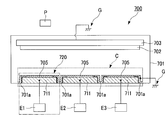
- FIG. 10A shows an example of a conventional film forming apparatus 700 using a sputtering method (Patent Document 1).
- the film forming apparatus 700 includes a plurality of cathodes 720.
- FIG. 10B is an enlarged cross-sectional view showing one of the plurality of cathodes 720 shown in FIG. 10A (Patent Document 2).
- the cathode 720 includes a sputtering target, a cathode body 710, a cathode mounting flange 701a, an insulating plate 712, a power supply unit E1 (E2, E3), and a grounding unit G. Is done.
- the target is composed of a backing plate 704 and a base material 705 disposed on the main surface 704a of the backing plate, is provided inside the chamber 701, and is attached to the cathode body 710 using a plurality of bolt members.
- magnetic field generation units H1 H2, H3 that generate leakage magnetic flux on the surface of the base material 705 are provided.
- a circulation channel composed of a channel 708a into which cooling water is introduced and a channel 708b into which cooling water is led out in order to control the temperature of the target.
- the cathode body 710 is provided inside the chamber 701 and is attached to the cathode attachment flange 711 using a plurality of bolt members via an insulating plate 712.
- the cathode mounting flange 711 is grounded.
- the backing plate 704 and the cathode body 710 are covered with a ground shield 701a in which an opening for exposing the base material 705 to a space (film formation space) in the chamber is formed.
- the ground shield 701a is provided in order to suppress discharge in a portion other than the base material 705.
- the ground shield 701a is normally attached to the chamber (wall portion) 701 using a plurality of bolt members while being grounded.
- a sputtered film (film formed by sputtering) can be formed uniformly.
- the sputtered film can be formed uniformly on the object to be processed 702.
- the base material of the sputtering target provided in each cathode 720 is only one type. That is, the conventional film forming apparatus 700 has a configuration in which only a film forming process using one kind of base material is performed. Therefore, when performing a plurality of types of film forming processes continuously, it is necessary to use separate chambers corresponding to the types of film forming, and it is necessary to provide a plurality of spaces in which the chambers are installed. In addition, every time processing is completed, it is necessary to transfer the object to be processed to a chamber for performing the next processing.
- the time required for the work to transport the object to be processed and the time required for the work (process) to exhaust the gas in the chamber in accordance with the process of carrying the object in and out of the chamber are generated.
- the time from the end of the process to the start of the next process becomes longer.
- the time required for the film forming process is shortened.
- the present invention has been made in consideration of such circumstances, and in one film formation space, a first sputtered film formed by a base material provided on one surface of one backing plate, and one backing plate.
- the second sputtered film formed by the base material provided on the other surface has a width corresponding to the area of a large number of base materials and is placed on the target object that is stationary so as to face the base material.
- An object is to provide a cathode unit that can be formed uniformly.
- the cathode unit of one embodiment of the present invention is used in a film forming apparatus, and the cathode unit includes a first main surface, a second main surface located on the opposite side to the first main surface, and a first side surface (one of the first main surface). Side surface), and a backing plate having a second side surface (the other side surface) located on the opposite side of the first side surface, a first base material disposed on the first main surface, and a second main surface A second base material disposed, and a rotating shaft penetrating the backing plate from the first side surface toward the second side surface, wherein the plurality of rotating shafts are arranged in parallel to each other in the same plane.
- a plurality of targets provided in the film formation space and the rotation shaft are rotated, and a voltage used for sputtering is applied to the target via the rotation shaft, and each of the plurality of targets is supported.
- a plurality of control units provided to Provided at a position (on the non-sputtering surface side of the backing plate) close to the surface of the backing plate away from the film forming space so that a specific distributed magnetic field is generated on the surface of the backing plate close to the film forming space. And a plurality of magnetic field generation units.
- the first side surface and the second side surface are perpendicular to the longitudinal direction of the backing plate, and the shapes of the first side surface and the second side surface are rectangular. Is preferred.
- each backing plate has a side portion parallel to the longitudinal direction of the backing plate, and an adhesion preventing plate is disposed on the side portion via an insulating member. It is preferable that Moreover, it is preferable that the said adhesion prevention board adjacent to each other is provided with the convex part.
- the first side surface and the second side surface are perpendicular to the longitudinal direction of the backing plate, and the shapes of the first side surface and the second side surface are trapezoids. Is preferred.
- the first side surface and the second side surface are perpendicular to the longitudinal direction of the backing plate, and the shape of the first side surface and the second side surface is a parallelogram. Preferably there is.
- each backing plate preferably has a side portion parallel to the longitudinal direction of the backing plate, and the side portion is preferably formed in a stepped shape.
- each backing plate preferably has a side portion parallel to the longitudinal direction of the backing plate, and the side portion is preferably formed in a wave shape.
- each of the backing plates has side portions parallel to the longitudinal direction of the backing plate, and one of the side portions adjacent to each other has a convex portion.
- the other side part preferably has a recess. That is, it is preferable that one side is formed in a convex shape and the other side is formed in a concave shape.
- the cathode unit according to the present invention includes a plurality of cathodes, and the total area of the base material exposed to the film formation space in the plurality of cathodes (the total area of the sputtering surface) is defined as the area to be processed of the object to be processed. It can be the same level.
- Each cathode includes a sputtering target in which a base material is individually arranged on each of the two main surfaces of the cathode.
- Each target has a configuration that can be rotated by a rotation shaft that penetrates the side surface (a rotation shaft that is provided so as to penetrate the backing plate from the first side surface toward the second side surface). ing.
- both of the two main surfaces of each target can be used as the sputtering processing surface, and both of the base materials arranged on the two main surfaces can be applied to the sputtering processing.
- the second sputtered film formed of the base material provided on the substrate can be uniformly formed on the object to be processed.
- such a first sputtered film and a second sputtered film are uniformly formed on an object to be processed that has a width corresponding to the total area of a large number of base materials and is placed stationary so as to face the base material. Can be formed.
- first film formation process first type film formation process
- second film formation process second type film formation process
- FIG. 10 is a cross-sectional view of a plurality of targets according to Modification 2.
- FIG. 10 is a cross-sectional view of a plurality of targets according to Modification 3.
- FIG. It is sectional drawing of the some target which concerns on embodiment of this invention.
- the target which concerns on the modification 6 Comprising: It is an expanded sectional view which shows the area
- FIG. 10 is a cross-sectional view of a plurality of targets according to Modification 2.
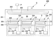
- FIG. 1A is a diagram illustrating a configuration of a film forming apparatus 200 including a cathode unit 220 according to an embodiment of the present invention.
- the film forming apparatus 200 includes a sputtering chamber 201 and a cathode unit 230 formed by a plurality of cathodes 220.
- An exhaust device (exhaust portion) P for exhausting the inside of the chamber 201 is attached to the wall portion of the chamber 201.
- Each cathode 220 includes sputtering targets C1, C2, and C3, control units E1, E2, and E3 connected to the targets C1, C2, and C3, respectively, and magnetic field generation units H1, H2, and H3.
- FIG. 1A although the structure provided with three targets is shown as an example, the number of targets is not limited to this embodiment.
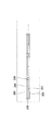
- FIG. 1B is an enlarged perspective view of the targets C1, C2, and C3 constituting each cathode 220 in FIG. 1A.
- Each of the backing plates 204 constituting the targets C1, C2, and C3 has a rotation shaft 207 perpendicular to the longitudinal direction L, and the rotation shaft 207 is directed from the first side surface 211 toward the second side surface 212. It penetrates.
- Each of the rotating shafts 207 is electrically connected to the control units E1, E2, and E3, and can be rotated using the control units E1, E2, and E3. Then, the backing plate 204 rotates in conjunction with the rotation of each rotating shaft 207. In order to achieve stable rotation, it is desirable that the rotating shaft 207 penetrates the center of gravity of the backing plate 204.
- Each of the control units E1, E2, E3 includes a rotation drive unit, a power supply unit, and a cooling water circulation unit.
- a rotation drive part rotates the rotating shaft 207 with which target C1, C2, C3 was equipped.
- the power supply unit applies a voltage (power) used for sputtering to the targets C1, C2, and C3.
- the cooling water circulation unit supplies the cooling water used for controlling the temperatures of the targets C1, C2, and C3 to the targets C1, C2, and C3, and discharges the cooling water from the targets C1, C2, and C3.
- Each of the targets C 1, C 2, and C 3 is disposed at a position facing a table (support table) 203 that supports a substrate to be processed (object to be processed) 202 in the chamber 201.
- the support base 203 is grounded through the grounding part G.
- Each of the targets C1, C2, and C3 includes a backing plate 204 having a flat shape, a first base material 205 disposed on a first main surface 204a (one main surface) of the backing plate 204, and a second main surface 204b. It is comprised with the 2nd preform
- each backing plate 204 As the material constituting each backing plate 204, a material having high conductivity, thermal conductivity, and low gas releasing property is desirably used, and copper or stainless steel is mainly used. Further, the first main surfaces of all the backing plates 204 are arranged so as to form one surface, and the second main surfaces of all the backing plates 204 are arranged so as to form one surface. Accordingly, the surfaces of the plurality of base materials exposed in the film formation space 50 are positioned on the same surface.
- the surface of the base material exposed in the film formation space 50 is a surface on which an inert gas such as Ar gas collides when the sputtering process is performed.
- the first base material 205 and the second base material 206 a material of a film formed on the substrate to be processed 202 such as a metal or an insulator is used.
- the main surface of the backing plate 204 which is the sputtering treatment surface, for the types (material types) of the first base material 205 and the second base material 206 arranged on the first main surface and the second main surface of all the backing plates 204
- the types of all base materials arranged in the same are the same (unified). Further, as will be described later, even if the base material used for the sputtering process is changed by the rotation of the rotating shaft 207, the types of all the base materials arranged on the main surface (sputtering process surface) of the backing plate 204 are the same. It is.
- the first base material 205 and the second base material 206 may be made of the same material or different materials.
- Each of the magnetic field generation units H1, H2, and H3 is located away from the film formation space 50 (a region where sputtering is performed) so that a specific distributed magnetic field is generated on the surface of the backing plate 204 close to the film formation space 50. And, it is arranged at a position close to the surface of the backing plate 204 (non-sputtering processing surface side).
- the “non-sputtered surface” of the backing plate 204 is a first main surface 204a or a second main surface 204b and is a base material not used for sputtering (the first base material 205 or the second base surface 204b). This means the main surface on which the base material 206) is placed.
- the “sputtering surface” of the backing plate 204 is the first main surface 204a or the second main surface 204b, and a base material (first base material 205 or second base material 206) used for sputtering is placed on the backing plate 204. It means a main surface that is placed at a position close to the film formation space 50. Such “non-sputtering surface” and “sputtering surface” are switched as the backing plate 204 rotates. When the first main surface 204a is a non-sputtering surface, the second main surface 204b is sputtered.
- the second main surface 204b is a non-sputtering processing surface.
- Each part of the magnetic flux generated by the magnetic field generation units H1, H2, and H3 penetrates the backing plate 204 from the non-sputtering processing surface toward the sputtering processing surface, and is a mother disposed on the sputtering processing surface of the backing plate 204. It leaks to the surface of the material (first base material 205 in FIG. 1). In the region where the magnetic flux leaks, the base material is sputtered in a concentrated manner by converging the plasma, so that the film can be formed at a high speed.
- each of the magnetic field generation units H1, H2, and H3 is disposed so as to be close to the second base material 206 and separated from the target C when performing the sputtering process using the first base material 205.
- the leakage magnetic flux is generated on the surface of the first base material 205.
- each of the magnetic field generation units H1, H2, and H3 is disposed so as to be close to the first base material 205 and away from the target C when performing the sputtering process using the second base material 206.
- the leakage magnetic flux is generated on the surface of the second base material 205.
- each of the magnetic field generation units H1, H2, and H3 is preferably disposed at a position close to the targets C1, C2, and C3.
- each of the magnetic field generation units H1, H2, and H3 includes a retreat drive unit (H11, H21, and H31).
- the evacuation drive units (H11, H21, H31) are devices for controlling the positions of the magnetic field generation units H1, H2, H3.
- the magnetic field generation units H1, H2, H3 are placed at positions close to the targets C1, C2, C3. Arrange. Further, when the targets C1, C2, and C3 rotate, the retracting drive units (H11, H21, and H31) retract the magnetic field generating units H1, H2, and H3 outside the rotational radius of the targets C1, C2, and C3. Let The retreat drive unit (H11, H21, H31) moves the targets C1, C2, C3 to normal positions (positions close to the targets C1, C2, C3, targets C1, C2) after the rotation of the targets C1, C2, C3 is completed. , C3).
- each of the magnetic field generation units H1, H2, and H3 may be normally positioned outside the rotation radius of the targets C1, C2, and C3. Only during the sputtering process, the retract drive unit (H11, H21, H31) moves the magnetic field generators H1, H2, H3 to positions close to the targets C1, C2, C3, and after the sputtering process is completed, the retract drive is performed. The units (H11, H21, H31) may return the magnetic field generation units H1, H2, H3 to the normal positions.
- each of the magnetic field generation units H1, H2, and H3 includes a swing drive unit (H12, H22, and H32).
- the swing drive units (H12, H22, H32) swing the magnetic field generation units H1, H2, H3 in a direction parallel to the main surfaces (204a, 204b) of the backing plate 204.
- the swing drive unit (H12, H22, H32) is in at least one of a direction perpendicular to the longitudinal direction L of the targets C1, C2, C3 and a direction parallel to the longitudinal direction L of the targets C1, C2, C3.
- the magnetic field generator H is swung.
- the magnetic flux generated by the magnetic field generators H1, H2, and H3 can be evenly leaked to the surface of the base material disposed at a position close to the sputtering surface of each target C1, C2, and C3. it can.
- a region where the plasma converges is uniformly formed on the surface of the base material. Therefore, the erosion generated on the surface of the base material by the sputtering treatment is made uniform, and the utilization efficiency of each target C1, C2, C3 can be improved.
- the film-forming process which improved the uniformity of in-plane distribution can be performed with respect to the surface of the to-be-processed substrate 202.
- FIG. 2 is a view showing the targets C1, C2, and C3 constituting each cathode 220 according to the embodiment of the present invention shown in FIG. 1B, and is a cross-sectional view corresponding to a plane perpendicular to the longitudinal direction L thereof.
- a circulation channel (a first circulation channel and a second circulation channel) that is formed at a position close to the second main surface 204b and configured by channels 208a and 208b.
- a circulation channel) is formed. Cooling water flows through the circulation channel. The cooling water is introduced from one of the channels 208a and 208b and led out from the other. By causing the cooling water to flow through the circulation channels 208a and 208b, the temperature rise of the first base material 205 and the second base material 206 during the sputtering process can be suppressed.
- each of the rotating shafts 207 is connected to the control units E1, E2, and E3.
- the sputtering voltage applied to each backing plate 204 is supplied from the control units E1, E2, and E3 to the backing plate 204 via a power supply line provided in each rotating shaft 207.
- the cooling water flowing through the circulation channels 208a and 208b is supplied to the circulation channel from the control units E1, E2, and E3 via the cooling water supply and discharge lines provided in the rotary shafts 207.
- a deposition preventing plate 209 is provided on the side portion 213 parallel to the longitudinal direction L of the backing plate 204.
- the deposition preventing plate 209 is grounded and prevents particles generated during the sputtering process from entering the side surface of the backing plate 204.
- an insulating member 209a is disposed between the deposition preventing plate 209 and the backing plate 204, and the insulating member 209a prevents the deposition preventing plate 109 from being damaged by a voltage supplied during sputtering.
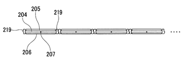
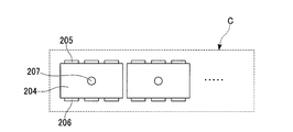
- 3A and 3B are views of a plurality of targets C (C1, C2, C3) constituting the cathode unit 230 of FIG. 1A as viewed from one end side of the rotating shaft 207.
- the targets C are arranged in a line so that all the rotation axes 207 are parallel to each other.
- the target adhesion preventing plates 209 adjacent to each other are arranged so as to approach each other.
- one of the deposition plates (first deposition plate) is disposed so as to approach the other deposition plate (second deposition plate).
- the surfaces where both of the adhesion preventing plates are opposed to each other have a shape in which the adhesion preventing plates do not overlap each other.
- a convex portion (convex inclined portion) is provided in a substantially central region of the surfaces of the adhesion preventing plates 209 (outer surfaces of the adhesion preventing plates 209) facing each other.
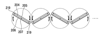
- each target can be rotated (reversed) in an individual rotation direction and rotation speed.
- the adhesion prevention plates 209 adjacent to the targets are close to each other so as not to prevent the rotation of each target. It is desirable.
- the target adhesion preventing plates 209 adjacent to each other are arranged so as to approach each other.
- one of the deposition plates first deposition plate
- the other deposition plate second deposition plate.
- the surfaces where both of the adhesion preventing plates are opposed to each other have a shape in which the adhesion preventing plates do not overlap each other.
- a flat portion is formed on the surface (half surface) of one of the deposition plates 209 with the center of the surfaces of the deposition plates 209 facing each other (the outer surface of the deposition plate 209) as a boundary.
- a convex inclined portion is formed on the surface (half surface) of the other deposition preventing plate 209.
- the convex inclined portion has two inclined surfaces.
- One inclined surface is a surface rising at a steep angle from the flat portion, and is a steeply inclined surface located at the center of the target.
- the other inclined surface is a gently inclined surface extending from the top of the convex inclined portion toward the outside of the deposition preventing plate 209.
- the adhesion prevention board 209 which mutually opposes, it has approached so that the mutually adjacent steeply inclined surface may mesh
- FIG. 4A to 4C are diagrams for explaining an example of the rotation operation of the target shown in FIG. 3B.
- a plurality of targets are arranged in a line so that all the rotating shafts 207 are included so as to be arranged in parallel and on the same plane.
- the main surfaces of all the backing plates 204 on which the first base material 205 is arranged are located on the same surface and face the same direction on the sputtering processing surface (not shown).
- FIG. 4B each target is rotated about the rotation axis 207. At this time, a pair of adjacent targets are rotated in opposite directions.
- each target is rotated so that the rotation speed of the target becomes the same.
- FIG. 4C the main surfaces of all the backing plates 204 on which the first base material 205 is disposed are located on the same surface and face the same direction on the surface opposite to the sputtering surface. ing.
- the cathode unit according to the embodiment of the present invention is composed of a plurality of cathodes, and the total area of the sputtering treatment surfaces of the plurality of cathodes and the area to be processed of the object to be processed can be made comparable.
- Each cathode includes a sputtering target in which a base material is individually arranged on each of the two main surfaces of the cathode.
- each target can be rotated by a rotation shaft that penetrates the side surface (a rotation shaft 207 that is provided so as to penetrate the backing plate 204 from the first side surface 211 toward the second side surface 212).
- the main surface facing the object to be processed and the main surface not facing the object to be processed can be changed in the same chamber. That is, both of the two main surfaces of each target can be used as the sputtering processing surface, and both of the base materials arranged on the two main surfaces can be applied to the sputtering processing.
- the second sputtered film formed from the provided base material can be uniformly formed on the object to be processed.
- such a first sputtered film and a second sputtered film are uniformly formed on an object to be processed that has a width corresponding to the total area of a large number of base materials and is placed stationary so as to face the base material. Can be formed.
- the space for installing the chambers necessary for the film forming process is reduced as compared with the conventional technique using a separate chamber for each type of film forming process. be able to.
- first film formation process first type film formation process
- second film formation process second type film formation process
- each of the magnetic field generation units H1, H2, and H3 is not provided in the backing plate 204 but is disposed at a position separated from the backing plate 204. Therefore, in each cathode 220, the leakage magnetic flux can be generated on the surfaces of the two base materials using only one magnetic field generation unit.
- the second base material 206 and the first base material 205 are made of the same material, one target is used as compared with the case where the base material disposed only on one main surface of the backing plate is used as in the prior art.
- the per-use period can be extended.
- the number of times of replacement of the base material can be reduced, and the number of exhaust operations in the chamber 201 (step of reducing the pressure of the chamber 201 from the atmospheric pressure to the vacuum) that occurs when the base material is replaced is reduced. be able to.
- each of the first base material 205 and the second base material 206 is made of a material that forms a lower layer and an upper layer of a laminated film formed on the substrate to be processed 102, using only one target, Two film-forming processes can be performed continuously. Then, by performing two successive film formation processes in the same chamber, the gas in the chamber is exhausted between the film formation process using the first base material 205 and the film formation process using the second base material 206.
- a process (process) such as a process and a transfer of a substrate to be processed becomes unnecessary, and the time required for such a process (process) can be shortened.
- the first base material 205 is disposed so as to face the first main surface 204a of the backing plate 204, and the second base material 206 is placed on the second main surface 204b of the backing plate 204. Arrange to face each other.
- the first base material 205 is joined to the first main surface 204a of the backing plate 204 using a first adhesive member (not shown). More specifically, the first adhesive member is applied to the first main surface 204a of the backing plate 204 that forms the bonding surface, and the backing plate 204 and the first adhesive member are heated and melted at a temperature equal to or higher than the melting point. Then, the first base material 205 is placed on the melted first adhesive member, and the first adhesive member melted between the first base material 205 and the backing plate 204 is cooled to room temperature.
- the first adhesive member used in this step is preferably a low melting point metal, for example, indium.
- the backing plate 204 and the first base material 205 are joined in a high temperature state and cooled to room temperature in the joined state. And the backing plate 204 is compressed with cooling.
- the first base material 205 is bonded only to the first main surface 204a, the compression rate of the backing plate 204 on the first main surface 204a and the compression rate of the backing plate 204 on the second main surface 204 are Different. Therefore, the backing plate 204 has a shape in which the first main surface 204a or the second main surface 204b is warped in a convex shape.
- FIG. 5B shows an example in which the backing plate 204 has a convex warp on the first main surface 204a.
- a convex warp may occur on the two principal surfaces 204b.
- the backing plate 204 warped by the joining of the first base material 205 and the backing plate 204 is shaped so as to have a flat shape.
- the method of shaping the backing plate 204 is not limited to a specific method, in the present embodiment, pressure is applied to the second main surface 204b of the backing plate 204 in a direction opposite to the direction in which the warping occurs. Use mechanical correction methods.
- the second base material 206 is joined to the second main surface 204b of the backing plate 204 using a second adhesive member (not shown). More specifically, the second adhesive member is applied to the second main surface 204b of the backing plate 204 that forms the bonding surface, and the backing plate 204 and the second adhesive member are heated and melted at a temperature equal to or higher than the melting point. Then, the second base material 206 is disposed on the melted second adhesive member, and is cooled to room temperature in a state where the melted second adhesive member is sandwiched between the second base material 206 and the backing plate 204.
- the second adhesive member used in this step is preferably a low melting point metal, for example, indium.
- the backing plate 204 and the second base material 206 are bonded in a high temperature state and cooled to room temperature while being bonded. And the backing plate 204 is compressed with cooling.
- the first base material 205 is joined to the first main surface 204a and the second base material 206 is joined to the second main surface 204b
- the compression rate of the backing plate 204 on the first main surface 204a is different. Therefore, the backing plate 204 has a shape in which the first main surface 204a or the second main surface 204b is warped in a convex shape.
- the backing plate 204 warped by the joining of the second base material 206 and the backing plate 204 is shaped so as to have a flat shape.
- the method of shaping the backing plate 204 is not limited to a specific method, but in the present embodiment, a method of mechanically correcting the backing plate 204 by applying a pressure in a direction opposite to the direction in which the warping occurs. Is used.
- the adhesion preventing plate 209 is joined to the side surface parallel to the longitudinal direction L of the backing plate 204 by using an insulating adhesive member (insulating member) 209a.
- the target of the embodiment is formed.
- first base material 205 and the second base material 206 are joined to the backing plate 204 in this order, but the joining order may be reversed.
- the target manufacturing method of the embodiment of the present invention it is not necessary to provide a fixing region in the base material as in the case of fixing the base material to the backing plate using a fixing member such as a bolt or a clamp. Therefore, the entire area of the first base material 205 and the second base material 206 arranged on the respective main surfaces of the backing plate 204 can be used for sputtering.
- the backing plate warped by the bonding becomes a flat shape.
- Shape as follows. Therefore, it is possible to manufacture a target in which a base material having a flat surface is bonded to each of the two main surfaces of the backing plate. Accordingly, since the base material and the substrate to be processed are arranged in parallel, the sputtered particles popping out from the base material can be uniformly deposited on the processing surface of the substrate to be processed, thereby forming a film.
- 5A to 5F show an example of a method of joining the first base material 205 and the second base material 206 to the main surfaces of the backing plate 204 using an adhesive member.
- a method of fixing the first base material 205 and the second base material 206 to each main surface of the backing plate 204 using a fixing member such as a clamp is another example of fixing the first base material 205 and the second base material 206 to each main surface of the backing plate 204 using a fixing member such as a clamp.
- FIG. 6 is a view showing a modification of the target, and is a view of one of the plurality of targets C as viewed from one end side of the rotating shaft 607.
- the backing plate 204 of the above embodiment is formed of a single plate
- the backing plate 614 of the first modification is formed of a plywood in which two plates (backing plates) 604 and 611 are overlapped.
- circulation channels 608a and 608b are formed at positions close to the first main surface 614a that is the outermost surface of the backing plate, and cooling water flows, and a second main surface that is the outermost surface of the backing plate.
- Circulating flow paths 613a and 613b are provided at positions close to the surface 614b and through which cooling water flows.
- the same members as those in the first embodiment are denoted by the same reference numerals, and the description thereof is omitted or simplified.
- the circulation channels 608a and 608b for the cooling water are formed in the backing plate 604 at positions close to either the first main surface 604a or the second main surface 604b.
- the circulation channels 608a and 608b for the cooling water are formed in the backing plate 614 at positions close to both the first main surface 214a and the second main surface 614b. Therefore, according to the structure of the modification 1, the target which has a high cooling function with respect to both the 1st base material 605 and the 2nd base material 612 can be obtained.
- a base material used for sputtering is disposed on each of the two main surfaces which are the outermost surfaces of the backing plate. Therefore, in the chamber, after performing the sputtering process using the first base material 605 disposed on the first main surface 614a, the target is reversed and the second base material 612 disposed on the second main surface 614b. Can be used for sputtering.
- the second base material 612 is made of the same material as the first base material 605, one target is used as compared with the case where the base material disposed only on one main surface of the backing plate is used as in the prior art.
- the per-use period can be extended. Thereby, the frequency
- each of the first base material 605 and the second base material 612 is made of a material that forms the lower layer and the upper layer of the laminated film formed on the substrate to be processed, only one target is used. Two film forming processes can be performed continuously. Then, by performing two successive film forming processes in the same chamber, the gas in the chamber is exhausted between the film forming process using the first base material 605 and the film forming process using the second base material 612. A process (process) such as a process and a transfer of a substrate to be processed becomes unnecessary, and the time required for such a process (process) can be shortened.
- the first base material 605 is joined to the first main surface 604a of the backing plate 604 using the first adhesive member. More specifically, the first adhesive member is applied to the first main surface 604a of the backing plate 604 that forms the bonding surface, and the backing plate 604 and the first adhesive member are heated and melted at a temperature equal to or higher than the melting point. Then, the first base material 605 is disposed on the melted first adhesive member, and cooled to room temperature with the melted first adhesive member sandwiched between the first base material 605 and the backing plate 604.
- the first adhesive member used in this step is preferably a low melting point metal, for example, indium.
- the backing plate 604 and the first base material 605 are joined in a high temperature state and cooled to room temperature while being joined. And the backing plate 604 is compressed with cooling.
- the first base material 605 is bonded only to the first main surface 604a, the compression rate of the backing plate 604 on the first main surface 604a and the compression rate of the backing plate 604 on the second main surface 604b are Different. Therefore, the backing plate 604 has a shape in which the first main surface 604a or the second main surface 604b is warped in a convex shape.
- the backing plate 604 warped by the joining of the first base material 605 and the backing plate 604 is shaped so as to have a flat shape.
- the method of shaping the backing plate 604 is not limited to a specific method, but in this modification, a method of mechanically correcting the backing plate 604 by applying pressure in a direction opposite to the direction in which the warping occurs. Is used.
- the second base material 612 is joined to the first main surface 611a of the backing plate 611 using the second adhesive member. More specifically, the second adhesive member is applied to the first main surface 611a of the backing plate 611 forming the bonding surface, and the backing plate 611 and the second adhesive member are heated and melted at a temperature equal to or higher than the melting point. Then, the second base material 612 is disposed on the melted second adhesive member, and cooled to room temperature in a state where the melted second adhesive member is sandwiched between the second base material 612 and the backing plate 611.
- the second adhesive member used in this step is preferably a low melting point metal, for example, indium.
- the backing plate 611 warped by the joining of the backing plate 611 and the second base material 612 is shaped so as to have a flat shape.
- the method of shaping the backing plate 611 is not limited to a specific method, but in this modification, a method of mechanically correcting the backing plate 611 by applying pressure in a direction opposite to the direction in which the warping occurs. Is used.
- the backing plate 604 and the backing plate 611 are joined using an adhesive member so that the second major surface 604b of the backing plate 604 and the second major surface 611b of the backing plate 611 face each other. .
- the adhesion modification plate 609 is joined to the side surface parallel to the longitudinal direction of the backing plate 614 using the insulating adhesive member (insulating member) 609a, whereby the target modification 1 is obtained. It is formed.
- first step to the second step and the third step to the fourth step may be performed by changing the order, or may be performed simultaneously.
- the backing plate 614 is formed in advance by superimposing the two plates 604 and 611, and then the target manufacturing method described above is performed in the same manner as the backing plate 604 in the embodiment of the present invention. It is also formed by using.
- the entire region of the first base material 605 and the second base material 612 disposed on the respective main surfaces of the backing plate 614 can be used for sputtering.
- the backing plate warped by the bonding is shaped so as to have a flat shape. To do. Therefore, it is possible to manufacture a target in which a base material having a flat surface is bonded to each of the two main surfaces of the backing plate. Accordingly, since the base material and the substrate to be processed are arranged in parallel, the sputtered particles popping out from the base material can be uniformly deposited on the processing surface of the substrate to be processed, thereby forming a film.
- FIG. 7A is a view of the plurality of targets C according to the first embodiment as viewed from one end side of the rotation shaft 207.
- FIG. 7B is a view of a plurality of targets C according to Modification 2 as viewed from one end side of the rotation shaft 207.
- FIG. 7C is a view of a plurality of targets C according to Modification 3 as viewed from one end side of the rotation shaft 207.
- vertical to the rotating shaft 207 of the backing plate which comprises each target is a rectangle.
- the cross section (cross section corresponding to the first side surface 211 and the second side surface 212) perpendicular to the rotation axis 207 of the backing plate constituting each target is a trapezoid.
- vertical to the rotating shaft 207 of the backing plate which comprises each target is a parallelogram.
- each of the backing plates 304 and 404 has a side surface (side portion) parallel to the longitudinal direction.
- the side surfaces of the backing plates are covered with each other so that one side surface and the other side surface of the backing plates adjacent to each other overlap. That is, in Modification 2 or Modification 3, each of the backing plates adjacent to each other functions as an adhesion preventing plate for the backing plate. Therefore, since the operation
- FIG. 8A is a view of a plurality of targets C as viewed from one end side of the rotation shaft 207.
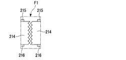
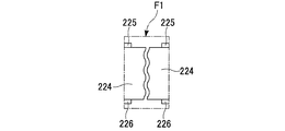
- 8B to 8D are enlarged sectional views showing a region F1 between two adjacent targets in FIG. 8A.
- Modification 4 shown in FIG. 8B corresponds to a modification of the structure of the first embodiment.
- Modification 5 shown in FIG. 8C corresponds to a modification of the structure of the first embodiment.
- Modification 6 shown in FIG. 8D corresponds to a modification of the structure of the first embodiment.
- the side part (side surface) parallel to the longitudinal direction of each said backing plate is formed in planar shape.
- the side part parallel to the longitudinal direction of each backing plate is formed in step shape.
- the side part parallel to the longitudinal direction of each backing plate is formed in the waveform.
- a convex part is formed in one side part among the side parts extended in parallel with the longitudinal direction of a mutually adjacent backing plate (one side part is convex). Formed), and a recess is formed on the other side (the other side is formed in a concave shape).
- each of the backing plates 214, 224, and 234 has a side surface (side portion) that extends parallel to the longitudinal direction.
- the side surfaces of the backing plates are covered with each other so that one side surface and the other side surface of the adjacent backing plates overlap each other. That is, in the modified examples 4, 5, and 6, each backing plate adjacent to each other functions as an adhesion preventing plate for the backing plate. Therefore, since the operation
- FIG. 9A is a view of a plurality of targets C as viewed from one end side of the rotation shaft 307.
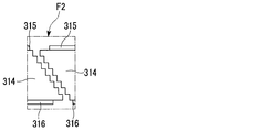
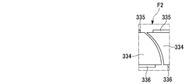
- 9B to 9D are enlarged sectional views showing a region F2 between two adjacent targets in FIG. 9A.
- Modification 7 shown in FIG. 9B shows an example in which Modification 2 described above is further modified.
- Modification 8 shown in FIG. 9C shows an example in which Modification 2 described above is further modified.
- the modified example 9 shown in FIG. 9D shows an example in which the modified example 2 described above is further modified.
- the side part (side surface) parallel to the longitudinal direction of each backing plate is formed in a planar shape.
- the side part parallel to the longitudinal direction of each backing plate is formed in step shape.
- the side part parallel to the longitudinal direction of each backing plate is formed in the waveform.
- a convex part is formed in one side part among the side parts extended in parallel with the longitudinal direction of a mutually adjacent backing plate (one side part is convex). Formed), and a recess is formed on the other side (the other side is formed in a concave shape).
- each backing plate 314, 324, 334 has a side surface (side portion) that extends in parallel to the longitudinal direction thereof.
- the side surfaces of the backing plates are covered with each other so that one side surface and the other side surface of the adjacent backing plates overlap each other. That is, in the modified examples 7, 8, and 9, each backing plate adjacent to each other functions as an adhesion preventing plate for the backing plate. Therefore, since the operation
- the present invention can be widely applied to a case where a film forming process by sputtering is performed on an object to be processed.
- SYMBOLS 200 Film-forming apparatus, 204 ... Backing plate, 204a, 204b ... Main surface, 205 ... First base material, 206 ... Second base material, 207 ... Rotating shaft, 209 ... Anti-adhesion plate, 209a ... Insulating member ... 209a, 230 ... Cathode unit, C1, C2, C3 ... Target, E1, E2, E3 ... Control part, H1, H2, H3: Magnetic field generator.
Landscapes
- Chemical & Material Sciences (AREA)
- Engineering & Computer Science (AREA)
- Physics & Mathematics (AREA)
- Plasma & Fusion (AREA)
- Analytical Chemistry (AREA)
- Chemical Kinetics & Catalysis (AREA)
- Materials Engineering (AREA)
- Mechanical Engineering (AREA)
- Metallurgy (AREA)
- Organic Chemistry (AREA)
- Physical Vapour Deposition (AREA)
Abstract
Description
本願は、2011年4月26日に出願された特願2011-098427号に基づき優先権を主張し、その内容をここに援用する。
一般的なスパッタリング装置では、チャンバ内にスパッタリング用のカソードが設けられ、減圧したチャンバ内において、カソードに取り付けられたターゲットと所定の間隔を空けて対向するように被処理体が配置される。
次に、チャンバ内にArガス(不活性ガス)を導入し、被処理体をグラウンドに接続した状態でターゲットに負の電圧を印加することにより放電させ、放電によりArガスから電離したArイオンをターゲットに衝突させる。
そして、ターゲットから飛び出す粒子を被処理体に付着させることにより、成膜処理が行われる。
成膜装置700は、複数のカソード720を備えている。図10Bは、図10Aに示す複数のカソード720のうち一つを示す拡大断面図(特許文献2)。
図10Bに示すように、カソード720は、スパッタリング用のターゲットと、カソード本体710と、カソード取り付けフランジ701aと、絶縁板712と、電力供給部E1(E2、E3)と、接地部Gとで構成される。
バッキングプレート704の内部には、母材705の表面上に漏洩磁束を生成する磁場生成部H1(H2、H3)が設けられている。
また、バッキングプレート704の内部には、ターゲットの温度を制御するために冷却水が導入される流路708aおよび冷却水が導出される流路708bで構成された循環流路が設けられている。
バッキングプレート704およびカソード本体710は、母材705をチャンバ内の空間(成膜空間)に露出させる開口が形成されたグラウンドシールド701aに覆われている。
グラウンドシールド701aは母材705以外の部分における放電を抑えるために設けられている。グラウンドシールド701aは、通常、接地された状態で、チャンバ(壁部)701に複数本のボルト部材を用いて取り付けられている。
したがって、複数種類の成膜処理を連続して行う場合には、成膜の種類ごとに対応した別々のチャンバを用いる必要があり、チャンバが設置される複数のスペースを設けなければならない。
また、処理が終わるたびに、被処理体を、次の処理を行うチャンバへ搬送する必要がある。そのため、被処理体の搬送作業に要する時間、及び被処理体をチャンバ内に搬入したり搬出したりする工程に伴ってチャンバ内の気体を排気する作業(工程)に要する時間が生じ、一つの処理が終わってから次の処理が始まるまでの時間が長くなる。その結果として、成膜処理するために必要な時間が短くなる。
そして、各々のカソードにおいては、カソードの二つの主面の各々に、母材が個別に配置されたスパッタリング用ターゲットを備えている。
また、各々のターゲットは、その側面を貫通させた回転軸(第1側面から第2側面に向けてバッキングプレートを貫通するように設けられた回転軸)により、回転させることが可能な構成を備えている。
このような構成において、ターゲットを回転させることにより、同一チャンバ内において、被処理体と対向する主面と被処理体と対向してない主面とを変更することができる。
すなわち、各々のターゲットが有する二つの主面の両方をスパッタリング処理面として用いることができ、二つの主面に配置された母材の両方を、スパッタリング処理に適用することができる。
したがって、第1成膜処理の成膜処理が終わってから第2成膜処理が始まるまでの時間を短縮することができ、成膜処理するために必要な時間を、従来技術を用いる場合に比べて長く設けることができる。
図1Aは、本発明の実施形態に係るカソードユニット220を備えた、成膜装置200の構成について説明する図である。
成膜装置200は、スパッタリング用のチャンバ201および複数のカソード220で形成されたカソードユニット230とで構成されている。
チャンバ201の壁部には、チャンバ201内を排気する排気装置(排気部)Pが付設されている。
各々のカソード220は、スパッタリング用のターゲットC1,C2,C3と、ターゲットC1,C2,C3とそれぞれ接続された制御部E1,E2,E3と、磁場生成部H1,H2,H3とを有する。
なお、図1Aでは、ターゲットを三つ備えた構成を一例として示しているが、ターゲットの数は、本実施形態に限定されない。
ターゲットC1,C2,C3を構成するバッキングプレート204の各々は、その長手方向Lに垂直な回転軸207を有し、回転軸207は、第1側面211から第2側面212に向けてバッキングプレート204を貫通している。
回転軸207の各々は、制御部E1,E2,E3と電気的に接続され、制御部E1,E2,E3を用いて回転させることができる。
そして、各々の回転軸207の回転に連動して、バッキングプレート204が回転する。
安定した回転を実現するために、回転軸207はバッキングプレート204の重心を貫通していることが望ましい。
ターゲットC1,C2,C3の各々は、チャンバ201内において、被処理基板(被処理体)202を支持する台(支持台)203と対向する位置に配置される。支持台203は、接地部Gを通じて接地されている。
全てのバッキングプレート204の第1主面及び第2主面に配置される第一母材205及び第二母材206の種類(材料の種類)について、スパッタリング処理面であるバッキングプレート204の主面に配置される全ての母材の種類は同じである(統一されている)。また、後述するように、回転軸207の回転によってスパッタリング処理に使用される母材が変更されても、バッキングプレート204の主面(スパッタリング処理面)に配置される全ての母材の種類は同じである。なお、第一母材205と第二母材206とは、同じ材料で構成されていてもよいし、異なる材料で構成されていてもよい。
以下の説明において、バッキングプレート204の「非スパッタリング処理面」とは、第1主面204a又は第2主面204bであって、スパッタリングに用いられていない母材(第一母材205又は第二母材206)が載置されている主面を意味する。
また、バッキングプレート204の「スパッタリング処理面」とは、第1主面204a又は第2主面204bであって、スパッタリングに用いられる母材(第一母材205又は第二母材206)が載置され、成膜空間50に近い位置に配置される主面を意味する。
このような「非スパッタリング処理面」及び「スパッタリング処理面」は、バッキングプレート204の回転に伴って切り替わり、第1主面204aが非スパッタリング処理面である場合には、第2主面204bがスパッタリング処理面となり、第1主面204aがスパッタリング処理面である場合には、第2主面204bが非スパッタリング処理面となる。
磁場生成部H1,H2,H3により生成される磁束の一部の各々は、バッキングプレート204を非スパッタリング処理面からスパッタリング処理面に向けて貫通し、バッキングプレート204のスパッタリング処理面に配置された母材(図1では第一母材205)の表面に漏洩する。
磁束の漏洩した領域においては、プラズマが収束することにより、集中的に母材がスパッタリングされるため、高速での成膜することが可能となる。
また、磁場生成部H1,H2,H3の各々は、第二母材206を用いてスパッタリング処理を行う場合には、第一母材205に近い位置であってターゲットCと離間するように配置され、漏洩磁束を第二母材205の表面に生成する。
そこで、本発明の実施形態に係る磁場生成部H1,H2,H3の各々は、退避駆動部(H11,H21,H31)を備えている。退避駆動部(H11,H21,H31)は、磁場生成部H1,H2,H3の位置を制御する装置であり、通常、ターゲットC1,C2,C3に近い位置に磁場生成部H1,H2,H3を配置させる。また、ターゲットC1,C2,C3が回転する際には、退避駆動部(H11,H21,H31)は、ターゲットC1,C2,C3の回転半径よりも外側に磁場生成部H1,H2,H3を退避させる。退避駆動部(H11,H21,H31)は、ターゲットC1,C2,C3の回転が終了した後に、ターゲットC1,C2,C3を通常の位置(ターゲットC1,C2,C3に近い位置、ターゲットC1,C2,C3の回転半径よりも内側)に戻す。
この揺動により、磁場生成部H1,H2,H3によって生成される磁束を、各ターゲットC1,C2,C3のスパッタリング処理面に近い位置に配置された母材の表面に、均一に漏洩させることができる。
漏洩磁束を均一に発生させることにより、母材の表面においてプラズマが収束する領域が一様に形成される。
そのため、スパッタリング処理によって母材表面に生じるエロージョンが均一化され、各ターゲットC1,C2,C3の利用効率を向上させることができる。
そして、被処理基板202の表面に対して、面内分布の均一性を高めた成膜処理を行うことができる。
ターゲットC1,C2,C3の各々を構成するバッキングプレート204内において、第2主面204bに近い位置に形成され、流路208a及び208bで構成された循環流路(第1循環流路及び第2循環流路)が形成されている。循環流路には、冷却水が流動する。
冷却水は、流路208aおよび208bのうち、一方から導入され、他方から導出される。循環流路208aおよび208bに冷却水を流すことにより、スパッタリング処理中の第一母材205および第二母材206の温度上昇を抑えることができる。
各バッキングプレート204に印加するスパッタリング電圧は、制御部E1,E2,E3から、各回転軸207内に設けられた電力供給ラインを介してバッキングプレート204に供給される。
また、循環流路208a、208bを流れる冷却水は、制御部E1,E2,E3から、各回転軸207内に設けられた冷却水の供給および排出用ラインを介して、循環流路に供給される。
防着板209は、接地されており、スパッタリング処理中に発生した粒子がバッキングプレート204の側面に回り込むのを防ぐ。
また、防着板209とバッキングプレート204との間には絶縁部材209aが配置され、絶縁部材209aは、スパッタリング時に供給される電圧によって防着板109にダメージが発生することを防ぐ。
ターゲットCは、全ての回転軸207が互いに平行となるように、一列に並んでいる。
したがって、各ターゲットを、個別の回転方向および回転速度で回転(反転)させることができる。
ただし、スパッタリング処理中に発生した粒子を、非スパッタリング処理面側の空間に回り込みにくくするために、ターゲットの隣り合う防着板209は、各々のターゲットの回転を妨げないように、接近していることが望ましい。
初めに、図4Aに示すように、第一母材205が配置された全てのバッキングプレート204の主面は、同一面上に位置し、かつ、スパッタリング処理面(不図示)において同一方向を向いている。
次に、図4Bに示すように、回転軸207を中心として、各ターゲットを回転させる。このとき、一対の隣り合うターゲットは、互いに反対方向に回転させる。また、ターゲットの回転速度が同じになるように、各ターゲットを回転させる。
そして、図4Cに示すように、第一母材205が配置された全てのバッキングプレート204の主面は、同一面上に位置し、かつ、スパッタリング処理面とは反対の面において同一方向を向いている。
そして、各々のカソードにおいては、カソードの二つの主面の各々に、母材が個別に配置されたスパッタリング用ターゲットを備えている。
また、各々のターゲットは、その側面を貫通させた回転軸(第1側面211から第2側面212に向けてバッキングプレート204を貫通するように設けられた回転軸207)により、回転可能である。
これらの構成を用いて、ターゲットを回転させることにより、同一チャンバ内において、被処理体と対向する主面と被処理体と対向してない主面とを変更することができる。
すなわち、各々のターゲットが有する二つの主面の両方をスパッタリング処理面として用いることができ、二つの主面に配置された母材の両方を、スパッタリング処理に適用することができる。
したがって、第1成膜処理の成膜処理が終わってから第2成膜処理が始まるまでの時間を短縮することができ、成膜処理するために必要な時間を、従来技術を用いる場合に比べて長く設けることができる。
したがって、各カソード220において、一つの磁場生成部のみを用いて、二つの母材の各々の表面に、漏洩磁束を生成することができる。
これにより、母材の交換回数を減らすことができ、母材の交換にともなって生じるチャンバ201内の排気作業(チャンバ201の圧力が大気圧から真空になるように減圧する工程)の回数を減らすことができる。
そして、連続する二つの成膜処理を同一チャンバ内で行うことにより、第一母材205による成膜工程と第二母材206による成膜工程との間に行う、チャンバ内の気体を排気する工程及び被処理基板の搬送等の作業(工程)が不要となり、このような作業(工程)に要する時間を短縮することができる。
上記実施形態の構成を備えたターゲットの製造方法について、図5A~図5Fに示す工程図を用いて説明する。
まず、図5Aに示す第一工程において、第一母材205をバッキングプレート204の第1主面204aに対向するように配置し、第二母材206をバッキングプレート204の第2主面204bに対向するように配置する。
より具体的には、接合面を形成するバッキングプレート204の第1主面204aに第一接着部材を塗布し、バッキングプレート204及び第一接着部材を融点以上の温度で加熱して融解させる。
そして、融解した第一接着部材上に第一母材205を配置し、第一母材205とバッキングプレート204との間で融解した第一接着部材が挟まれた状態で室温まで冷却する。
この工程で用いる第一接着部材としては、低融点金属であることが望ましく、例えば、インジウムが用いられる。
そして、冷却にともなって、バッキングプレート204は圧縮される。
このとき、第1主面204aにのみ第一母材205が接合されているため、第1主面204aにおけるバッキングプレート204の圧縮率と、第2主面204におけるバッキングプレート204の圧縮率とは異なる。
したがって、バッキングプレート204は、第1主面204aあるいは第2主面204bにおいて、凸状に反りが生じた形状を有する。
バッキングプレート204を整形する方法は、特定の方法に限定されないが、本実施形態では、バッキングプレート204の第2主面204bに対し、反りが生じている方向とは逆の方向に圧力を加えて機械的に矯正する方法を用いる。
より具体的には、接合面を形成するバッキングプレート204の第2主面204bに第二接着部材を塗布し、バッキングプレート204及び第二接着部材を融点以上の温度で加熱して融解させる。
そして、融解した第二接着部材上に第二母材206を配置し、第二母材206とバッキングプレート204との間に融解した第二接着部材が挟まれた状態で室温まで冷却する。
この工程で用いる第二接着部材としては、低融点金属であることが望ましく、例えば、インジウムが用いられる。
そして、冷却にともなって、バッキングプレート204は圧縮される。
このとき、第1主面204aには第一母材205が接合され、第2主面204bには第二母材206が接合されているため、第1主面204aにおけるバッキングプレート204の圧縮率と、第2主面204bにおけるバッキングプレート204の圧縮率とは異なる。
したがって、バッキングプレート204は、第1主面204aあるいは第2主面204bにおいて、凸状に反りが生じた形状を有する。
バッキングプレート204を整形する方法は、特定の方法に限定されないが、本実施形態では、バッキングプレート204に対し、反りが生じている方向とは逆の方向に圧力を加えて機械的に矯正する方法を用いる。
したがって、バッキングプレート204のそれぞれの主面に配置された第一母材205および第二母材206の全域をスパッタリングに用いることができる。
したがって、バッキングプレートの二つの主面の各々に、個別に、表面が平坦な形状を有する母材が接合されたターゲットを製造することができる。
これにより、母材と被処理基板が平行に配置されるため、母材から飛び出すスパッタ粒子を被処理基板の処理面内に均一に付着させ、成膜することができる。
したがって、上記第三工程および第五工程に相当する工程は不要となり、より簡略化したプロセスでターゲットを製造することができる。
図6は、ターゲットの変形例を示す図であって、複数のターゲットCのうちの一つを、回転軸607の一端側から見た図である。
上記実施形態のバッキングプレート204は単板で形成されていたのに対し、変形例1のバッキングプレート614は、二枚の板(バッキングプレート)604および611が重ね合わされた合板で構成されている。
バッキングプレート614の内部には、バッキングプレートの最外面である第1主面614aに近い位置に形成され、冷却水が流動する循環流路608aおよび608bと、バッキングプレートの最外面である第2主面614bに近い位置に形成され、冷却水が流動する循環流路613aおよび613bとが設けられている。図6において、第1実施形態と同一部材には同一符号を付して、その説明は省略または簡略化する。
これに対し、変形例1の構成では、冷却水の循環流路608aおよび608bは、バッキングプレート614内において、第1主面214aおよび第2主面614bの両方に近い位置に形成される。
したがって、変形例1の構成によれば、第一母材605及び第二母材612の両方に対して高い冷却機能を有するターゲットを得ることができる。
そのため、チャンバ内において、第1主面614aに配置された第一母材605を用いてスパッタリング処理を行った後に、ターゲットを反転させて、第2主面614bに配置された第二母材612を用いてスパッタリング処理を行うことができる。
これにより、母材の交換回数を減らすことができ、交換にともなって発生する、チャンバ内の気体を排気する作業(工程)の回数を減らすことができる。
そして、連続する二つの成膜処理を同一チャンバ内で行うことにより、第一母材605による成膜工程と第二母材612による成膜工程との間に行う、チャンバ内の気体を排気する工程及び被処理基板の搬送等の作業(工程)が不要となり、このような作業(工程)に要する時間を短縮することができる。
上記変形例1の構成を備えたターゲットの製造方法の一例について説明する。
より具体的には、接合面を形成するバッキングプレート604の第1主面604aに第一接着部材を塗布し、バッキングプレート604及び第一接着部材を融点以上の温度で加熱して融解させる。
そして、融解した第一接着部材上に第一母材605を配置し、第一母材605とバッキングプレート604との間に融解した第一接着部材を挟んだ状態で室温まで冷却する。
この工程で用いる第一接着部材としては、低融点金属であることが望ましく、例えば、インジウムが用いられる。
そして、冷却にともなって、バッキングプレート604は圧縮される。
このとき、第1主面604aにのみ第一母材605が接合されているため、第1主面604aにおけるバッキングプレート604の圧縮率と、第2主面604bにおけるバッキングプレート604の圧縮率とは異なる。
したがって、バッキングプレート604は、第1主面604aあるいは第2主面604bにおいて、凸状に反りが生じた形状を有する。
バッキングプレート604を整形する方法は、特定の方法に限定されないが、本変形例では、バッキングプレート604に対し、反りが生じている方向とは逆の方向に圧力を加えて機械的に矯正する方法を用いる。
より具体的には、接合面を形成するバッキングプレート611の第1主面611aに第二接着部材を塗布し、バッキングプレート611及び第二接着部材を融点以上の温度で加熱して融解させる。
そして、融解した第二接着部材上に第二母材612を配置し、第二母材612とバッキングプレート611との間に融解した第二接着部材が挟まれた状態で室温まで冷却する。
この工程で用いる第二接着部材としては、低融点金属であることが望ましく、例えば、インジウムが用いられる。
バッキングプレート611を整形する方法は、特定の方法に限定されないが、本変形例では、バッキングプレート611に対し、反りが生じている方向とは逆の方向に圧力を加えて機械的に矯正する方法を用いる。
したがって、バッキングプレート614のそれぞれの主面に配置された第一母材605および第二母材612の全域をスパッタリングに用いることができる。
したがって、バッキングプレートの二つの主面の各々に、個別に、表面が平坦な形状を有する母材が接合されたターゲットを製造することができる。
これにより、母材と被処理基板が平行に配置されるため、母材から飛び出すスパッタ粒子を被処理基板の処理面内に均一に付着させ、成膜することができる。
図7Aは、第一実施形態に係る複数のターゲットCを回転軸207の一端側から見た図である。
図7Bは、変形例2に係る複数のターゲットCを回転軸207の一端側から見た図である。
図7Cは、変形例3に係る複数のターゲットCを回転軸207の一端側から見た図である。
第一実施形態では、各々のターゲットを構成するバッキングプレートの回転軸207に垂直な断面は、長方形である。
これに対し、変形例2では、各々のターゲットを構成するバッキングプレートの回転軸207に垂直な断面(第1側面211及び前記第2側面212に対応する断面)は、台形である。また、変形例3では、各々のターゲットを構成するバッキングプレートの回転軸207に垂直な断面は、平行四辺形である。
すなわち、変形例2または変形例3においては、互いに隣接する各々のバッキングプレートは、バッキングプレートの防着板として機能する。
そのため、バッキングプレートの長手方向に平行な側面に、第一実施形態において用いられるような防着板を取り付ける作業が発生しないため、個々のターゲットを製造する方法(工程)を簡略化することができる。
図8Aは、複数のターゲットCを回転軸207の一端側から見た図である。
図8B~図8Dは、図8Aにおける、隣り合う二つのターゲットの間の領域F1を示す拡大断面図である。図8Bに示す変形例4は、第一実施形態の構造の変形例に相当する。図8Cに示す変形例5は、第一実施形態の構造の変形例に相当する。図8Dに示す変形例6は、第一実施形態の構造の変形例に相当する。
第一実施形態では、各々の前記バッキングプレートの長手方向に平行な側部(側面)が平面状に形成されている。
これに対し、図8Bに示す変形例4においては、各々のバッキングプレートの長手方向に平行な側部が、階段状に形成されている。
また、図8Cに示す変形例5においては、各々のバッキングプレートの長手方向に平行な側部が、波状に形成されている。
また、図8Dに示す変形例6においては、互いに隣り合うバッキングプレートの長手方向に平行に延在する側部のうち、一方の側部に凸部が形成され(一方の側部が凸状に形成され)、他方の側部に凹部が形成されている(他方の側部が凹状に形成されている)。
すなわち、変形例4、5、6においては、互いに隣接する各々のバッキングプレートは、バッキングプレートの防着板として機能する。
そのため、バッキングプレートの長手方向に平行な側面に、第一実施形態において用いられるような防着板を取り付ける作業が発生しないため、個々のターゲットを製造する方法(工程)を簡略化することができる。
図9B~図9Dは、図9Aにおける、隣り合う二つのターゲットの間の領域F2を示す拡大断面図である。図9Bに示す変形例7は、上述の変形例2を更に変形させた例を示している。図9Cに示す変形例8は、上述の変形例2を更に変形させた例を示している。図9Dに示す変形例9は、上述の変形例2を更に変形させた例を示している。
変形例2では、各々のバッキングプレートの長手方向に平行な側部(側面)が平面状に形成されている。
これに対し、図9Bに示す変形例7においては、各々のバッキングプレートの長手方向に平行な側部が、階段状に形成されている。
また、図9Cに示す変形例8においては、各々のバッキングプレートの長手方向に平行な側部が、波状に形成されている。
また、図9Dに示す変形例9においては、互いに隣り合うバッキングプレートの長手方向に平行に延在する側部のうち、一方の側部に凸部が形成され(一方の側部が凸状に形成され)、他方の側部に凹部が形成されている(他方の側部が凹状に形成されている)。
すなわち、変形例7、8、9においては、互いに隣接する各々のバッキングプレートは、バッキングプレートの防着板として機能する。
そのため、バッキングプレートの長手方向に平行な側面に、第一実施形態において用いられるような防着板を取り付ける作業が発生しないため、個々のターゲットを製造する方法(工程)を簡略化することができる。
Claims (9)
- 成膜装置に用いられるカソードユニットであって、
第1主面,前記第1主面とは反対側に位置する第2主面,第1側面,及び前記第1側面とは反対側に位置する第2側面を有するバッキングプレートと、前記第1主面に配置された第一母材と、前記第2主面に配置された第二母材と、前記第1側面から前記第2側面に向けて前記バッキングプレートを貫通する回転軸とを有し、複数の回転軸は、互いに平行に並ぶように同一面内に配置されており、成膜空間内に設けられた複数のターゲットと、
前記回転軸を回転させ、前記回転軸を介して前記ターゲットにスパッタリングに用いられる電圧を印加し、複数のターゲットの各々に対応するように設けられた複数の制御部と、
前記成膜空間に近い前記バッキングプレートの面に特定の分布磁場が生成されるように、前記成膜空間から離れた前記バッキングプレートの面に近い位置に設けられた複数の磁場生成部とを含む
ことを特徴とするカソードユニット。 - 請求項1に記載のカソードユニットであって、
前記第1側面及び前記第2側面は、前記バッキングプレートの長手方向に垂直であり、前記第1側面及び前記第2側面の形状は、長方形である
ことを特徴とするカソードユニット。 - 請求項1又は請求項2に記載のカソードユニットであって、
各々の前記バッキングプレートは、前記バッキングプレートの長手方向に平行な側部を有し、
前記側部には、絶縁部材を介して、防着板が配置されている
ことを特徴とするカソードユニット。 - 請求項3に記載のカソードユニットであって、
互いに隣り合う前記防着板には、凸部が設けられている
ことを特徴とするカソードユニット。 - 請求項1に記載のカソードユニットであって、
前記第1側面及び前記第2側面は、前記バッキングプレートの長手方向に垂直であり、前記第1側面及び前記第2側面の形状は、台形である
ことを特徴とするカソードユニット。 - 請求項1に記載のカソードユニットであって、
前記第1側面及び前記第2側面は、前記バッキングプレートの長手方向に垂直であり、前記第1側面及び前記第2側面の形状は、平行四辺形である
ことを特徴とするカソードユニット。 - 請求項1、2、5、6のいずれか一項に記載のカソードユニットであって、
各々の前記バッキングプレートは、前記バッキングプレートの長手方向に平行な側部を有し、
前記側部は、階段状に形成されている
ことを特徴とするカソードユニット。 - 請求項1、2、5、6のいずれか一項に記載のカソードユニットであって、
各々の前記バッキングプレートは、前記バッキングプレートの長手方向に平行な側部を有し、
前記側部は、波状に形成されている
ことを特徴とするカソードユニット。 - 請求項1、2、5、6のいずれか一項に記載のカソードユニットであって、
各々の前記バッキングプレートは、前記バッキングプレートの長手方向に平行な側部を有し、
互いに隣り合う前記側部のうち、一方の側部は凸部を有し、他方の側部は凹部を有する
ことを特徴とするカソードユニット。
Priority Applications (5)
| Application Number | Priority Date | Filing Date | Title |
|---|---|---|---|
| KR1020167000324A KR20160008660A (ko) | 2011-04-26 | 2011-11-21 | 캐소드 유닛 |
| JP2013511870A JP5869560B2 (ja) | 2011-04-26 | 2011-11-21 | カソードユニット |
| KR1020137025829A KR20130133015A (ko) | 2011-04-26 | 2011-11-21 | 캐소드 유닛 |
| KR1020177024739A KR20170104160A (ko) | 2011-04-26 | 2011-11-21 | 캐소드 유닛 |
| CN201180069851.6A CN103459653B (zh) | 2011-04-26 | 2011-11-21 | 阴极单元 |
Applications Claiming Priority (2)
| Application Number | Priority Date | Filing Date | Title |
|---|---|---|---|
| JP2011-098427 | 2011-04-26 | ||
| JP2011098427 | 2011-04-26 |
Publications (1)
| Publication Number | Publication Date |
|---|---|
| WO2012147228A1 true WO2012147228A1 (ja) | 2012-11-01 |
Family
ID=47071766
Family Applications (1)
| Application Number | Title | Priority Date | Filing Date |
|---|---|---|---|
| PCT/JP2011/076759 Ceased WO2012147228A1 (ja) | 2011-04-26 | 2011-11-21 | カソードユニット |
Country Status (5)
| Country | Link |
|---|---|
| JP (2) | JP5869560B2 (ja) |
| KR (3) | KR20170104160A (ja) |
| CN (2) | CN105671500B (ja) |
| TW (1) | TWI495745B (ja) |
| WO (1) | WO2012147228A1 (ja) |
Families Citing this family (5)
| Publication number | Priority date | Publication date | Assignee | Title |
|---|---|---|---|---|
| KR102182582B1 (ko) | 2017-06-28 | 2020-11-24 | 가부시키가이샤 아루박 | 스퍼터 장치 |
| JP6602495B2 (ja) | 2017-06-29 | 2019-11-06 | 株式会社アルバック | 成膜装置 |
| JP2019210517A (ja) * | 2018-06-05 | 2019-12-12 | 株式会社アルバック | スパッタリング装置及び成膜方法 |
| KR20210036064A (ko) | 2019-09-25 | 2021-04-02 | 이현우 | 휴대용 보조배터리 |
| KR20220095642A (ko) | 2020-12-30 | 2022-07-07 | 전찬희 | 보조배터리발찌 |
Citations (5)
| Publication number | Priority date | Publication date | Assignee | Title |
|---|---|---|---|---|
| JPS59143067A (ja) * | 1983-02-02 | 1984-08-16 | Matsushita Electric Ind Co Ltd | スパツタリング装置 |
| US6224718B1 (en) * | 1999-07-14 | 2001-05-01 | Veeco Instruments, Inc. | Target assembly for ion beam sputter deposition with multiple paddles each having targets on both sides |
| JP2003147519A (ja) * | 2001-11-05 | 2003-05-21 | Anelva Corp | スパッタリング装置 |
| JP2004292871A (ja) * | 2003-03-26 | 2004-10-21 | Japan Aviation Electronics Industry Ltd | イオンビームスパッタ装置 |
| JP2006233240A (ja) * | 2005-02-22 | 2006-09-07 | Canon Inc | スパッタ用カソード及びスパッタ装置 |
Family Cites Families (14)
| Publication number | Priority date | Publication date | Assignee | Title |
|---|---|---|---|---|
| US4175030A (en) * | 1977-12-08 | 1979-11-20 | Battelle Development Corporation | Two-sided planar magnetron sputtering apparatus |
| GB2051877B (en) * | 1979-04-09 | 1983-03-02 | Vac Tec Syst | Magnetically enhanced sputtering device and method |
| JPH0734236A (ja) * | 1993-07-19 | 1995-02-03 | Canon Inc | 直流スパッタリング装置およびスパッタリング方法 |
| JP2002030430A (ja) * | 2000-07-17 | 2002-01-31 | Sony Corp | スパッタ装置 |
| JP4071520B2 (ja) * | 2002-03-29 | 2008-04-02 | キヤノンアネルバ株式会社 | スパッタリング装置 |
| JP2003328119A (ja) | 2002-05-14 | 2003-11-19 | Ulvac Japan Ltd | スパッタカソード |
| CN1439740A (zh) * | 2002-05-22 | 2003-09-03 | 甘肃工业大学 | 双面溅射的平面磁控溅射阴极 |
| JP4246547B2 (ja) * | 2003-05-23 | 2009-04-02 | 株式会社アルバック | スパッタリング装置、及びスパッタリング方法 |
| KR101275924B1 (ko) * | 2006-05-22 | 2013-06-14 | 엘지디스플레이 주식회사 | 스퍼터링 장치, 그 구동 방법 및 이를 이용한 패널 제조방법 |
| JP5265149B2 (ja) * | 2006-07-21 | 2013-08-14 | アプライド マテリアルズ インコーポレイテッド | マルチカソード設計用冷却暗部シールド |
| KR20100044230A (ko) | 2007-08-20 | 2010-04-29 | 가부시키가이샤 알박 | 스퍼터링 방법 및 스퍼터링 장치 |
| JP5322235B2 (ja) * | 2007-08-20 | 2013-10-23 | 株式会社アルバック | スパッタリング方法 |
| WO2010038271A1 (ja) * | 2008-09-30 | 2010-04-08 | キヤノンアネルバ株式会社 | スパッタリング装置および薄膜形成方法 |
| TW201038759A (en) * | 2009-04-30 | 2010-11-01 | Hon Hai Prec Ind Co Ltd | Magnetron sputtering apparatus |
-
2011
- 2011-11-21 KR KR1020177024739A patent/KR20170104160A/ko not_active Ceased
- 2011-11-21 KR KR1020137025829A patent/KR20130133015A/ko not_active Ceased
- 2011-11-21 CN CN201610219410.4A patent/CN105671500B/zh active Active
- 2011-11-21 CN CN201180069851.6A patent/CN103459653B/zh active Active
- 2011-11-21 KR KR1020167000324A patent/KR20160008660A/ko not_active Ceased
- 2011-11-21 JP JP2013511870A patent/JP5869560B2/ja active Active
- 2011-11-21 WO PCT/JP2011/076759 patent/WO2012147228A1/ja not_active Ceased
- 2011-11-22 TW TW100142798A patent/TWI495745B/zh active
-
2016
- 2016-01-06 JP JP2016001285A patent/JP6069540B2/ja active Active
Patent Citations (5)
| Publication number | Priority date | Publication date | Assignee | Title |
|---|---|---|---|---|
| JPS59143067A (ja) * | 1983-02-02 | 1984-08-16 | Matsushita Electric Ind Co Ltd | スパツタリング装置 |
| US6224718B1 (en) * | 1999-07-14 | 2001-05-01 | Veeco Instruments, Inc. | Target assembly for ion beam sputter deposition with multiple paddles each having targets on both sides |
| JP2003147519A (ja) * | 2001-11-05 | 2003-05-21 | Anelva Corp | スパッタリング装置 |
| JP2004292871A (ja) * | 2003-03-26 | 2004-10-21 | Japan Aviation Electronics Industry Ltd | イオンビームスパッタ装置 |
| JP2006233240A (ja) * | 2005-02-22 | 2006-09-07 | Canon Inc | スパッタ用カソード及びスパッタ装置 |
Also Published As
| Publication number | Publication date |
|---|---|
| TW201243076A (en) | 2012-11-01 |
| CN103459653B (zh) | 2016-05-04 |
| CN105671500B (zh) | 2018-10-12 |
| JP5869560B2 (ja) | 2016-02-24 |
| KR20160008660A (ko) | 2016-01-22 |
| JP2016041855A (ja) | 2016-03-31 |
| KR20130133015A (ko) | 2013-12-05 |
| KR20170104160A (ko) | 2017-09-14 |
| JPWO2012147228A1 (ja) | 2014-07-28 |
| TWI495745B (zh) | 2015-08-11 |
| CN103459653A (zh) | 2013-12-18 |
| CN105671500A (zh) | 2016-06-15 |
| JP6069540B2 (ja) | 2017-02-01 |
Similar Documents
| Publication | Publication Date | Title |
|---|---|---|
| JP6069540B2 (ja) | カソードユニット | |
| CN101100741B (zh) | 改进的pvd靶 | |
| JP5960384B2 (ja) | 静電チャック用基板及び静電チャック | |
| CN103764869B (zh) | 用于物理气相沉积腔室靶材的冷却环 | |
| JP7426773B2 (ja) | 物理的気相堆積処理システムのターゲットの冷却 | |
| JP6559233B2 (ja) | マグネトロンスパッタリング装置 | |
| JP6641472B2 (ja) | 成膜方法及びスパッタリング装置 | |
| JP5721817B2 (ja) | カソード | |
| JP5721815B2 (ja) | ターゲット及びターゲットの製造方法 | |
| JP4698055B2 (ja) | 高周波マグネトロンスパッタリング装置 | |
| JP6328089B2 (ja) | プラズマスパッタ装置 | |
| JP2007051337A (ja) | スパッタ電極及びスパッタ電極を備えたスパッタリング装置 | |
| JP7044887B2 (ja) | スパッタリング装置 | |
| JP2011089146A (ja) | スパッタリング装置およびスパッタリング方法 | |
| TW201437397A (zh) | 物理蒸氣沉積系統 | |
| KR20130111025A (ko) | 스퍼터링 멀티 타켓 어셈블리 및 이를 채용한 스퍼터링 증착 장비 |
Legal Events
| Date | Code | Title | Description |
|---|---|---|---|
| WWE | Wipo information: entry into national phase |
Ref document number: 201180069851.6 Country of ref document: CN |
|
| 121 | Ep: the epo has been informed by wipo that ep was designated in this application |
Ref document number: 11864547 Country of ref document: EP Kind code of ref document: A1 |
|
| ENP | Entry into the national phase |
Ref document number: 2013511870 Country of ref document: JP Kind code of ref document: A |
|
| ENP | Entry into the national phase |
Ref document number: 20137025829 Country of ref document: KR Kind code of ref document: A |
|
| NENP | Non-entry into the national phase |
Ref country code: DE |
|
| 122 | Ep: pct application non-entry in european phase |
Ref document number: 11864547 Country of ref document: EP Kind code of ref document: A1 |