WO2012137914A1 - 炭化珪素縦型電界効果トランジスタ - Google Patents
炭化珪素縦型電界効果トランジスタ Download PDFInfo
- Publication number
- WO2012137914A1 WO2012137914A1 PCT/JP2012/059489 JP2012059489W WO2012137914A1 WO 2012137914 A1 WO2012137914 A1 WO 2012137914A1 JP 2012059489 W JP2012059489 W JP 2012059489W WO 2012137914 A1 WO2012137914 A1 WO 2012137914A1
- Authority
- WO
- WIPO (PCT)
- Prior art keywords
- conductivity type
- silicon carbide
- region
- carbide layer
- conductive
- Prior art date
- Legal status (The legal status is an assumption and is not a legal conclusion. Google has not performed a legal analysis and makes no representation as to the accuracy of the status listed.)
- Ceased
Links
Images




Classifications
-
- H—ELECTRICITY
- H10—SEMICONDUCTOR DEVICES; ELECTRIC SOLID-STATE DEVICES NOT OTHERWISE PROVIDED FOR
- H10D—INORGANIC ELECTRIC SEMICONDUCTOR DEVICES
- H10D30/00—Field-effect transistors [FET]
- H10D30/60—Insulated-gate field-effect transistors [IGFET]
- H10D30/64—Double-diffused metal-oxide semiconductor [DMOS] FETs
- H10D30/66—Vertical DMOS [VDMOS] FETs
-
- H—ELECTRICITY
- H10—SEMICONDUCTOR DEVICES; ELECTRIC SOLID-STATE DEVICES NOT OTHERWISE PROVIDED FOR
- H10D—INORGANIC ELECTRIC SEMICONDUCTOR DEVICES
- H10D30/00—Field-effect transistors [FET]
- H10D30/60—Insulated-gate field-effect transistors [IGFET]
- H10D30/63—Vertical IGFETs
-
- H—ELECTRICITY
- H10—SEMICONDUCTOR DEVICES; ELECTRIC SOLID-STATE DEVICES NOT OTHERWISE PROVIDED FOR
- H10D—INORGANIC ELECTRIC SEMICONDUCTOR DEVICES
- H10D62/00—Semiconductor bodies, or regions thereof, of devices having potential barriers
- H10D62/10—Shapes, relative sizes or dispositions of the regions of the semiconductor bodies; Shapes of the semiconductor bodies
- H10D62/102—Constructional design considerations for preventing surface leakage or controlling electric field concentration
- H10D62/103—Constructional design considerations for preventing surface leakage or controlling electric field concentration for increasing or controlling the breakdown voltage of reverse-biased devices
- H10D62/105—Constructional design considerations for preventing surface leakage or controlling electric field concentration for increasing or controlling the breakdown voltage of reverse-biased devices by having particular doping profiles, shapes or arrangements of PN junctions; by having supplementary regions, e.g. junction termination extension [JTE]
-
- H—ELECTRICITY
- H10—SEMICONDUCTOR DEVICES; ELECTRIC SOLID-STATE DEVICES NOT OTHERWISE PROVIDED FOR
- H10D—INORGANIC ELECTRIC SEMICONDUCTOR DEVICES
- H10D62/00—Semiconductor bodies, or regions thereof, of devices having potential barriers
- H10D62/10—Shapes, relative sizes or dispositions of the regions of the semiconductor bodies; Shapes of the semiconductor bodies
- H10D62/102—Constructional design considerations for preventing surface leakage or controlling electric field concentration
- H10D62/103—Constructional design considerations for preventing surface leakage or controlling electric field concentration for increasing or controlling the breakdown voltage of reverse-biased devices
- H10D62/105—Constructional design considerations for preventing surface leakage or controlling electric field concentration for increasing or controlling the breakdown voltage of reverse-biased devices by having particular doping profiles, shapes or arrangements of PN junctions; by having supplementary regions, e.g. junction termination extension [JTE]
- H10D62/108—Constructional design considerations for preventing surface leakage or controlling electric field concentration for increasing or controlling the breakdown voltage of reverse-biased devices by having particular doping profiles, shapes or arrangements of PN junctions; by having supplementary regions, e.g. junction termination extension [JTE] having localised breakdown regions, e.g. built-in avalanching regions
-
- H—ELECTRICITY
- H10—SEMICONDUCTOR DEVICES; ELECTRIC SOLID-STATE DEVICES NOT OTHERWISE PROVIDED FOR
- H10D—INORGANIC ELECTRIC SEMICONDUCTOR DEVICES
- H10D62/00—Semiconductor bodies, or regions thereof, of devices having potential barriers
- H10D62/10—Shapes, relative sizes or dispositions of the regions of the semiconductor bodies; Shapes of the semiconductor bodies
- H10D62/17—Semiconductor regions connected to electrodes not carrying current to be rectified, amplified or switched, e.g. channel regions
- H10D62/393—Body regions of DMOS transistors or IGBTs
-
- H—ELECTRICITY
- H10—SEMICONDUCTOR DEVICES; ELECTRIC SOLID-STATE DEVICES NOT OTHERWISE PROVIDED FOR
- H10D—INORGANIC ELECTRIC SEMICONDUCTOR DEVICES
- H10D84/00—Integrated devices formed in or on semiconductor substrates that comprise only semiconducting layers, e.g. on Si wafers or on GaAs-on-Si wafers
- H10D84/101—Integrated devices comprising main components and built-in components, e.g. IGBT having built-in freewheel diode
- H10D84/141—VDMOS having built-in components
- H10D84/148—VDMOS having built-in components the built-in components being breakdown diodes, e.g. Zener diodes
-
- H—ELECTRICITY
- H10—SEMICONDUCTOR DEVICES; ELECTRIC SOLID-STATE DEVICES NOT OTHERWISE PROVIDED FOR
- H10D—INORGANIC ELECTRIC SEMICONDUCTOR DEVICES
- H10D62/00—Semiconductor bodies, or regions thereof, of devices having potential barriers
- H10D62/10—Shapes, relative sizes or dispositions of the regions of the semiconductor bodies; Shapes of the semiconductor bodies
- H10D62/13—Semiconductor regions connected to electrodes carrying current to be rectified, amplified or switched, e.g. source or drain regions
- H10D62/149—Source or drain regions of field-effect devices
- H10D62/151—Source or drain regions of field-effect devices of IGFETs
- H10D62/156—Drain regions of DMOS transistors
- H10D62/157—Impurity concentrations or distributions
-
- H—ELECTRICITY
- H10—SEMICONDUCTOR DEVICES; ELECTRIC SOLID-STATE DEVICES NOT OTHERWISE PROVIDED FOR
- H10D—INORGANIC ELECTRIC SEMICONDUCTOR DEVICES
- H10D62/00—Semiconductor bodies, or regions thereof, of devices having potential barriers
- H10D62/80—Semiconductor bodies, or regions thereof, of devices having potential barriers characterised by the materials
- H10D62/83—Semiconductor bodies, or regions thereof, of devices having potential barriers characterised by the materials being Group IV materials, e.g. B-doped Si or undoped Ge
- H10D62/832—Semiconductor bodies, or regions thereof, of devices having potential barriers characterised by the materials being Group IV materials, e.g. B-doped Si or undoped Ge being Group IV materials comprising two or more elements, e.g. SiGe
- H10D62/8325—Silicon carbide
Definitions
- the present invention relates to a silicon carbide vertical field effect transistor.
- a silicon carbide vertical field effect transistor such as a vertical MOSFET (MOS field effect transistor) is conventionally used in a semiconductor device as a switching device formed on a silicon carbide substrate. Yes.
- a silicon carbide vertical MOSFET will be described as an example of the silicon carbide vertical field effect transistor, but it goes without saying that the present invention is not limited to this.
- FIG. 6 shows a cross-sectional structure of an N-channel MOSFET which is one of conventional silicon carbide (hereinafter abbreviated as “SiC”) field effect transistors.
- N-type SiC layer 2 is formed on the surface of N-type SiC substrate 1
- a plurality of P-type regions 3 are formed on the surface of N-type SiC layer 2
- N-type source region 4 and P-type region 3 are formed on the surface of P-type region 3.
- a P-type contact region 5 is formed, and a source electrode 8 is formed on the surfaces of the N-type source region 4 and the P-type contact region 5.
- a gate electrode 7 is formed on the surface of the P-type region 3 between the N-type source 5 and the N-type SiC layer via a gate insulating film 6.
- a drain electrode 9 is formed on the back side.
- FIG. 7 is a cross-sectional structure diagram of another N-channel MOSFET formed using a P-type SiC layer on the surface.
- N-type SiC layer 2 is formed on the surface of N-type SiC substrate 1, and a plurality of P-type regions 10 are formed on the surface of N-type SiC layer 2. Further, a P-type SiC layer 11 is formed on the surface. Further, an N-type region 12 is formed in the P-type SiC layer 11 on the N-type SiC layer 2 where the P-type region 10 is not formed, and the N-type source region 4 and the P-type are formed on the surface of the P-type silicon carbide layer 11.
- a contact region 5 is formed, and a source electrode 8 is formed on the surfaces of the N-type source region 4 and the P-type contact region 5.
- a gate electrode 7 is formed on the surface of the P-type region 3 between the N-type source 5 and the N-type silicon carbide layer via a gate insulating film 6.
- a drain electrode 9 is formed on the back side.
- the present invention realizes a silicon carbide vertical field effect transistor capable of improving the breakdown resistance of a gate insulating film without applying a large electric field to the gate insulating film when a high voltage is applied to the drain electrode. This is the issue.
- a silicon carbide vertical field effect transistor having an electrode a high concentration is provided under the second conductivity type region. Silicon carbide vertical field effect transistor and forming a second conductive type region.
- first conductivity type silicon carbide substrate a low-concentration first conductivity type silicon carbide layer formed on the surface of the first conductivity type silicon carbide substrate, and selectively on the surface of the first conductivity type silicon carbide layer;
- the formed second conductivity type region, the first conductivity type silicon carbide layer and the second conductivity type silicon carbide layer formed on the surface of the second conductivity type region, and the first conductivity type silicon carbide layer A first conductivity type region selectively formed on the conductivity type silicon carbide layer, a first conductivity type source region formed in the second conductivity type silicon carbide layer, and a second conductivity type silicon carbide layer;
- a high concentration second conductivity type region formed between the first conductivity type source regions and a source electrode electrically connected to the high concentration second conductivity type region and the first conductivity type source region are adjacent to each other.
- the first conductive type A silicon carbide vertical field effect transistor characterized by forming a high-concentration second conductivity type region under a second conductivity type region formed in a silicon carbide layer.
- a second conductivity type region; a source electrode electrically connected to the high-concentration second conductivity type region and the first conductivity type source region; and a first conductivity type source region formed in the adjacent second conductivity type region A gate insulating film formed on the second conductive type region and the first conductive silicon carbide layer, a gate electrode formed on the gate insulating film, and a drain on the back surface side of the first conductive silicon carbide substrate.
- a part of the second conductivity type region is shallow Silicon carbide vertical field effect transistor, characterized in that it is formed.
- the formed second conductivity type region, the first conductivity type silicon carbide layer and the second conductivity type silicon carbide layer formed on the surface of the second conductivity type region, and the first conductivity type silicon carbide layer A first conductivity type region selectively formed on the conductivity type silicon carbide layer, a first conductivity type source region formed in the second conductivity type silicon carbide layer, and a second conductivity type silicon carbide layer; A high concentration second conductivity type region formed between the first conductivity type source regions and a source electrode electrically connected to the high concentration second conductivity type region and the first conductivity type source region are adjacent to each other.
- the first conductive type A silicon carbide vertical field effect transistor characterized in that a part of the second conductivity type region formed in the silicon carbide layer is shallow.
- the formed second conductivity type region, the first conductivity type silicon carbide layer and the second conductivity type silicon carbide layer formed on the surface of the second conductivity type region, and the first conductivity type silicon carbide layer A first conductivity type region selectively formed on the conductivity type silicon carbide layer, a first conductivity type source region formed in the second conductivity type silicon carbide layer, and a second conductivity type silicon carbide layer; A high concentration second conductivity type region formed between the first conductivity type source regions and a source electrode electrically connected to the high concentration second conductivity type region and the first conductivity type source region are adjacent to each other.
- the first conductive A silicon carbide vertical field effect transistor characterized in that the second conductivity type region formed in the silicon carbide layer is formed even under the first conductivity type region formed in the second conductivity type layer.
- the present invention when a high voltage is applied to the drain electrode, a large electric field is applied to the gate insulating film by causing avalanche to occur under a high concentration P region or in a region formed in a thin layer.
- a large electric field is applied to the gate insulating film by causing avalanche to occur under a high concentration P region or in a region formed in a thin layer.
- the silicon carbide vertical field effect transistor according to the present invention will be described in detail with reference to Examples 1 to 5.
- the present invention is not limited to the following first to fifth embodiments, and various design changes can be made without departing from the spirit of the present invention.
- FIG. 1 shows a cross-sectional structure of a MOSFET in the first embodiment of the present invention.
- the first conductivity type is N-type and the second conductivity type is P-type.
- an N-type SiC layer 2 is formed on the surface of an N-type SiC substrate 1, and a plurality of P-type regions 3 are formed on the surface of the N-type SiC layer 2.
- N-type source region 4 and a P-type contact region 5 are formed on the surface of the P-type region 3. Further, source electrodes 8 are formed on the surfaces of the N-type source region 4 and the P-type contact region 5.
- a high concentration P-type region 21 is formed under the P-type region 3. Further, on the surface of the P-type region 3 and the N-type SiC layer 2 sandwiched between the N-type source region 4 on the surface of the P-type region 3 and the N-type source region 4 on the surface of the P-type region 3 different from the P-type region 3.
- a gate electrode 7 is formed through a gate insulating film 6, and a drain electrode 9 is formed on the back surface side.
- the MOSFET in the structure of the first embodiment can be turned on by applying a voltage higher than the threshold voltage to the gate electrode and forming an inversion layer on the surface of the P-type region as in the conventional MOSFET.
- avalanche occurs at the PN junction portion between the high-concentration N-type SiC layer 2 in which a high voltage is applied to the drain electrode and the P-type region 21, thereby causing a large gate oxide film.
- An electric field is not applied, and the dielectric breakdown resistance of the gate insulating film when a high voltage is applied to the drain electrode can be improved, and the reliability of the gate insulating film can be improved.
- FIG. 2 shows a cross-sectional view of the MOSFET in the second embodiment of the present invention.
- N-type SiC layer 2 is formed on the surface of N-type carbide SiC substrate 1, and a plurality of P-type regions 3 are formed on the surface of N-type SiC layer 2. Further, a P-type SiC layer 11 is formed on the surface.
- An N-type region 12 is formed in the P-type SiC layer 11 so as to reach the N-type SiC layer 2.
- An N-type source region 4 and a P-type contact region 5 are formed on the surface of the P-type SiC layer 11. Further, source electrodes 8 are formed on the surfaces of the N-type source region 4 and the P-type contact region 5.
- a high concentration P-type region 21 is formed under the P-type region 3. Further, on the surface of the P-type region 3 and the N-type SiC layer 2 sandwiched between the N-type source region 4 on the surface of the P-type region 3 and the N-type source region 4 on the surface of the P-type region 3 different from the P-type region 3.
- a gate electrode 7 is formed through a gate insulating film 6, and a drain electrode 9 is formed on the back surface side. Also in the MOSFET formed in this way, avalanche occurs at the PN junction portion between the high-concentration N-type SiC layer 2 in which a high voltage is applied to the drain electrode and the P-type region 21, and a large electric field is generated in the gate oxide film.
- the breakdown resistance and reliability of the gate insulating film exhibit the same characteristics as in the first embodiment.
- FIG. 3 shows a cross-sectional view of a MOSFET according to Embodiment 3 of the present invention.
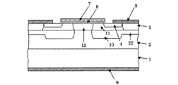
- the difference from the first embodiment is that a thin P-type region 22 is formed in a part of the P-type region 3 without forming the high-concentration P-type region 21. It is.
- avalanche occurs at the PN junction portion between the high-concentration N-type SiC layer 2 in which a high voltage is applied to the drain electrode and the thin P-type region 22, and a large gate oxide film is formed. No electric field is applied, and the dielectric breakdown resistance and reliability of the gate insulating film exhibit the same characteristics as in the first embodiment.
- FIG. 4 shows a cross-sectional view of a MOSFET according to the fourth embodiment of the present invention.
- the difference from the second embodiment is that a thin P-type region 22 is formed in a part of the P-type region 3 without forming the high-concentration P-type region 21. It is.
- avalanche occurs at the PN junction portion between the high-concentration N-type SiC layer 2 in which a high voltage is applied to the drain electrode and the thin P-type region 22, and a large gate oxide film is formed. No electric field is applied, and the dielectric breakdown resistance and reliability of the gate insulating film exhibit the same characteristics as in the first embodiment.
- FIG. 5 shows a cross-sectional view of a MOSFET in the fifth embodiment of the present invention.
- the basic structure is the same as that of the second embodiment.
- the difference from the second embodiment is that the P-type region 3 projects below the N-type region 12 without forming the high-concentration P-type region 21. It is a point that is formed.
- avalanche occurs at the PN junction portion of the high-concentration N-type SiC layer 2 in which a high voltage is applied to the drain electrode and the portion of the P-type region 3 that protrudes under the N-type region 12.
- a large electric field is not applied to the gate oxide film, and the dielectric breakdown resistance and reliability of the gate insulating film exhibit the same characteristics as in the first embodiment.
Landscapes
- Insulated Gate Type Field-Effect Transistor (AREA)
- Electrodes Of Semiconductors (AREA)
Abstract
Description
N型SiC基板1の表面にN型SiC層2が形成され、そのN型SiC層2の表面に複数のP型領域3が形成され、P型領域3の表面にはN型ソース領域4とP型コンタクト領域5が形成され、更にN型ソース領域4とP型コンタクト領域5との表面にソース電極8が形成されている。またN型ソース5の間のP型領域3とN型SiC層の表面にゲート絶縁膜6を介してゲート電極7が形成されている。また裏面側にはドレイン電極9が形成されている。
一方、ゲート電極7にゲート閾値以上の電圧を印可するとゲート電極7直下のP型領域3又はP型SiC層11の表面には反転層が形成されることにより電流が流れるため、ゲート電極7に印加する電圧によってMOSFETのスイッチング動作を行うことができる。
課題を解決するための手段
(1)第1導電型の炭化珪素基板と該第1導電型炭化珪素基板表面に形成された低濃度の第1導電型炭化珪素層と、該第1導電型炭化珪素層表面に選択的に形成された第2導電型領域と、該第2導領域内に形成された第1導電型ソース領域と、第2導電型領域内の第1導電型ソース領域の間に形成された高濃度の第2導電型領域と、該高濃度の第2導電型領域及び第1導電型ソース領域に電気的に接続するソース電極と、隣接する第2導電型領域に形成された第1導電型ソース領域から第2導電型領域及び第1導電型炭化珪素層の上に形成されたゲート絶縁膜と、該ゲート絶縁膜上に形成されたゲート電極と、第1導電型炭化珪素基板の裏面側にドレイン電極を備えた炭化珪素縦型電界効果トランジスタにおいて、第2導電型領域と第1導電型炭化珪素層との間にアバランシェ発生手段を設けたことを特徴とする炭化珪素縦型電界効果トランジスタ。
(2)第1導電型の炭化珪素基板と該第1導電型炭化珪素基板表面に形成された低濃度の第1導電型炭化珪素層と、該第1導電型炭化珪素層表面に選択的に形成された第2導電型領域と、該第2導領域内に形成された第1導電型ソース領域と、第2導電型領域内の第1導電型ソース領域の間に形成された高濃度の第2導電型領域と、該高濃度の第2導電型領域及び第1導電型ソース領域に電気的に接続するソース電極と、隣接する第2導電型領域に形成された第1導電型ソース領域から第2導電型領域及び第1導電型炭化珪素層の上に形成されたゲート絶縁膜と、該ゲート絶縁膜上に形成されたゲート電極と、第1導電型炭化珪素基板の裏面側にドレイン電極を備えた炭化珪素縦型電界効果トランジスタにおいて、第2導電型領域下に高濃度の第2導電型領域を形成することを特徴とする炭化珪素縦型電界効果トランジスタ。
(3)第1導電型の炭化珪素基板と該第1導電型炭化珪素基板表面に形成された低濃度の第1導電型炭化珪素層と、該第1導電型炭化珪素層表面に選択的に形成された第2導電型領域と、該第1導電型炭化珪素層及び第2導電型領域の表面に形成された第2導電型炭化珪素層と、該第2導電型炭化珪素層の第1導電型炭化珪素層上に選択的に形成された第1導電型領域と、第2導電型炭化珪素層内に形成された第1導電型ソース領域と、該第2導電型炭化珪素層内の第1導電型ソース領域の間に形成された高濃度の第2導電型領域と、該高濃度の第2導電型領域及び第1導電型ソース領域に電気的に接続するソース電極と、隣接する第2導電型炭化珪素層に形成された第1導電型ソース領域から第2導電型炭化珪素層及び第1導電型領域の上に形成されたゲート絶縁膜と、該ゲート絶縁膜上に形成されたゲート電極と、第1導電型炭化珪素基板の裏面側にドレイン電極を備えた炭化珪素縦型電界効果トランジスタにおいて、第1導電型炭化珪素層内に形成された第2導電型領域下に高濃度の第2導電型領域を形成することを特徴とする炭化珪素縦型電界効果トランジスタ。
(4)第1導電型の炭化珪素基板と該第1導電型炭化珪素基板表面に形成された低濃度の第1導電型炭化珪素層と、該第1導電型炭化珪素層表面に選択的に形成された第2導電型領域と、該第2導領域内に形成された第1導電型ソース領域と、第2導電型領域内の第1導電型ソース領域の間に形成された高濃度の第2導電型領域と、該高濃度の第2導電型領域及び第1導電型ソース領域に電気的に接続するソース電極と、隣接する第2導電型領域に形成された第1導電型ソース領域から第2導電型領域及び第1導電型炭化珪素層の上に形成されたゲート絶縁膜と、該ゲート絶縁膜上に形成されたゲート電極と、第1導電型炭化珪素基板の裏面側にドレイン電極を備えた炭化珪素縦型電界効果トランジスタにおいて、第2導電型領域の一部が浅く形成されていることを特徴とする炭化珪素縦型電界効果トランジスタ。
(5)第1導電型の炭化珪素基板と該第1導電型炭化珪素基板表面に形成された低濃度の第1導電型炭化珪素層と、該第1導電型炭化珪素層表面に選択的に形成された第2導電型領域と、該第1導電型炭化珪素層及び第2導電型領域の表面に形成された第2導電型炭化珪素層と、該第2導電型炭化珪素層の第1導電型炭化珪素層上に選択的に形成された第1導電型領域と、第2導電型炭化珪素層内に形成された第1導電型ソース領域と、該第2導電型炭化珪素層内の第1導電型ソース領域の間に形成された高濃度の第2導電型領域と、該高濃度の第2導電型領域及び第1導電型ソース領域に電気的に接続するソース電極と、隣接する第2導電型炭化珪素層に形成された第1導電型ソース領域から第2導電型炭化珪素層及び第1導電型領域の上に形成されたゲート絶縁膜と、該ゲート絶縁膜上に形成されたゲート電極と、第1導電型炭化珪素基板の裏面側にドレイン電極を備えた炭化珪素縦型電界効果トランジスタにおいて、第1導電型炭化珪素層に形成された第2導電型領域の一部が浅くなっていることを特徴とする炭化珪素縦型電界効果トランジスタ。
(6)第1導電型の炭化珪素基板と該第1導電型炭化珪素基板表面に形成された低濃度の第1導電型炭化珪素層と、該第1導電型炭化珪素層表面に選択的に形成された第2導電型領域と、該第1導電型炭化珪素層及び第2導電型領域の表面に形成された第2導電型炭化珪素層と、該第2導電型炭化珪素層の第1導電型炭化珪素層上に選択的に形成された第1導電型領域と、第2導電型炭化珪素層内に形成された第1導電型ソース領域と、該第2導電型炭化珪素層内の第1導電型ソース領域の間に形成された高濃度の第2導電型領域と、該高濃度の第2導電型領域及び第1導電型ソース領域に電気的に接続するソース電極と、隣接する第2導電型炭化珪素層に形成された第1導電型ソース領域から第2導電型炭化珪素層及び第1導電型領域の上に形成されたゲート絶縁膜と、該ゲート絶縁膜上に形成されたゲート電極と、第1導電型炭化珪素基板の裏面側にドレイン電極を備えた炭化珪素縦型電界効果トランジスタにおいて、該第1導電型炭化珪素層に形成された第2導電型領域が、第2導電型層に形成された第1導電型領域下にまで形成されていることを特徴とする炭化珪素縦型電界効果トランジスタ。
なお本発明は次の実施例1~5に限定されるものではなく、本発明の趣旨を逸脱することがなければ、種々の設計変更を行うことが可能である。
図1では、N型SiC基板1の表面にN型SiC層2が形成され、そのN型SiC層2の表面にP型領域3が複数形成されている。
また、P型領域3下には高濃度のP型領域21が形成されている。さらにP型領域3表面のN型ソース領域4と該P型領域3とは別のP型領域3表面のN型ソース領域4に挟まれたP型領域3とN型SiC層2の表面にはゲート絶縁膜6を介してゲート電極7が形成され、裏面側にドレイン電極9が形成されている。
このように形成されたMOSFETにおいて、ドレイン電極に高電圧が印加された高濃度のN型SiC層2とP型領域21のPN接合部分でアバランシェを起こすようになり、これによりゲート酸化膜に大きな電界が掛かることがなくなり、ドレイン電極に高電圧印加された場合のゲート絶縁膜の絶縁破壊耐量を向上させることができると共にゲート絶縁膜の信頼性を向上させることができる。
N型炭化SiC基板1の表面にN型SiC層2が形成され、そのN型SiC層2の表面にP型領域3が複数形成されている。更にその表面にはP型SiC層11が形成されている。P型SiC層11にはN型SiC層2にまで達するようにN型領域12が形成されている。
また、P型SiC層11の表面にはN型ソース領域4とP型コンタクト領域5が形成されている。さらにN型ソース領域4とP型コンタクト領域5との表面にソース電極8が形成されている。
このように形成されたMOSFETにおいても、ドレイン電極に高電圧が印加された高濃度のN型SiC層2とP型領域21のPN接合部分でアバランシェを起こすようになり、ゲート酸化膜に大きな電界が掛かることがなくなり、ゲート絶縁膜の絶縁破壊耐量及び信頼性は実施例1と同様の特性を示す。
基本的な構造は実施例1と同様であるが、実施例1と異なる点は高濃度のP型領域21を形成せずにP型領域3の一部を薄いP型領域22を形成する点である。
このように形成されたMOSFETにおいても、ドレイン電極に高電圧が印加された高濃度のN型SiC層2と薄いP型領域22のPN接合部分でアバランシェを起こすようになり、ゲート酸化膜に大きな電界が掛かることがなくなりゲート絶縁膜の絶縁破壊耐量及び信頼性は実施例1と同様の特性を示す。
基本的な構造は実施例2と同様であるが、実施例2と異なる点は高濃度のP型領域21を形成せずにP型領域3の一部を薄いP型領域22を形成する点である。
このように形成されたMOSFETにおいても、ドレイン電極に高電圧が印加された高濃度のN型SiC層2と薄いP型領域22のPN接合部分でアバランシェを起こすようになり、ゲート酸化膜に大きな電界が掛かることがなくなりゲート絶縁膜の絶縁破壊耐量及び信頼性は実施例1と同様の特性を示す。
基本的な構造は実施例2と同様であるが、実施例2と異なる点は、高濃度のP型領域21を形成せずにP型領域3がN型領域12の下まで張り出すように形成している点である。
このように形成されたMOSFETにおいても、ドレイン電極に高電圧が印加された高濃度のN型SiC層2とN型領域12下まで張り出した部分のP型領域3のPN接合部分でアバランシェを起こすようになり、ゲート酸化膜に大きな電界が掛かることがなくなりゲート絶縁膜の絶縁破壊耐量及び信頼性は実施例1と同様の特性を示す。
2 N型炭化珪素層
3 P型領域
4 Nソース領域
5 Pコンタクト領域
6 ゲート絶縁膜
7 ゲート電極
8 ソース電極
9 ドレイン電極
10 P型ベース領域
11 P型炭化珪素層
12 N型領域
21 高濃度P型領域
22 薄層P型領域
Claims (6)
- 第1導電型の炭化珪素基板と該第1導電型炭化珪素基板表面に形成された低濃度の第1導電型炭化珪素層と、該第1導電型炭化珪素層表面に選択的に形成された第2導電型領域と、該第2導領域内に形成された第1導電型ソース領域と、第2導電型領域内の第1導電型ソース領域の間に形成された高濃度の第2導電型領域と、該高濃度の第2導電型領域及び第1導電型ソース領域に電気的に接続するソース電極と、隣接する第2導電型領域に形成された第1導電型ソース領域から第2導電型領域及び第1導電型炭化珪素層の上に形成されたゲート絶縁膜と、該ゲート絶縁膜上に形成されたゲート電極と、第1導電型炭化珪素基板の裏面側にドレイン電極を備えた炭化珪素縦型電界効果トランジスタにおいて、第2導電型領域と第1導電型炭化珪素層との間にアバランシェ発生手段を設けたことを特徴とする炭化珪素縦型電界効果トランジスタ。
- 第1導電型の炭化珪素基板と該第1導電型炭化珪素基板表面に形成された低濃度の第1導電型炭化珪素層と、該第1導電型炭化珪素層表面に選択的に形成された第2導電型領域と、該第2導領域内に形成された第1導電型ソース領域と、第2導電型領域内の第1導電型ソース領域の間に形成された高濃度の第2導電型領域と、該高濃度の第2導電型領域及び第1導電型ソース領域に電気的に接続するソース電極と、隣接する第2導電型領域に形成された第1導電型ソース領域から第2導電型領域及び第1導電型炭化珪素層の上に形成されたゲート絶縁膜と、該ゲート絶縁膜上に形成されたゲート電極と、第1導電型炭化珪素基板の裏面側にドレイン電極を備えた炭化珪素縦型電界効果トランジスタにおいて、第2導電型領域下に高濃度の第2導電型領域を形成することを特徴とする炭化珪素縦型電界効果トランジスタ。
- 第1導電型の炭化珪素基板と該第1導電型炭化珪素基板表面に形成された低濃度の第1導電型炭化珪素層と、該第1導電型炭化珪素層表面に選択的に形成された第2導電型領域と、該第1導電型炭化珪素層及び第2導電型領域の表面に形成された第2導電型炭化珪素層と、該第2導電型炭化珪素層の第1導電型炭化珪素層上に選択的に形成された第1導電型領域と、第2導電型炭化珪素層内に形成された第1導電型ソース領域と、該第2導電型炭化珪素層内の第1導電型ソース領域の間に形成された高濃度の第2導電型領域と、該高濃度の第2導電型領域及び第1導電型ソース領域に電気的に接続するソース電極と、隣接する第2導電型炭化珪素層に形成された第1導電型ソース領域から第2導電型炭化珪素層及び第1導電型領域の上に形成されたゲート絶縁膜と、該ゲート絶縁膜上に形成されたゲート電極と、第1導電型炭化珪素基板の裏面側にドレイン電極を備えた炭化珪素縦型電界効果トランジスタにおいて、第1導電型炭化珪素層内に形成された第2導電型領域下に高濃度の第2導電型領域を形成することを特徴とする炭化珪素縦型電界効果トランジスタ。
- 第1導電型の炭化珪素基板と該第1導電型炭化珪素基板表面に形成された低濃度の第1導電型炭化珪素層と、該第1導電型炭化珪素層表面に選択的に形成された第2導電型領域と、該第2導領域内に形成された第1導電型ソース領域と、第2導電型領域内の第1導電型ソース領域の間に形成された高濃度の第2導電型領域と、該高濃度の第2導電型領域及び第1導電型ソース領域に電気的に接続するソース電極と、隣接する第2導電型領域に形成された第1導電型ソース領域から第2導電型領域及び第1導電型炭化珪素層の上に形成されたゲート絶縁膜と、該ゲート絶縁膜上に形成されたゲート電極と、第1導電型炭化珪素基板の裏面側にドレイン電極を備えた炭化珪素縦型電界効果トランジスタにおいて、第2導電型領域の一部が浅く形成されていることを特徴とする炭化珪素縦型電界効果トランジスタ。
- 第1導電型の炭化珪素基板と該第1導電型炭化珪素基板表面に形成された低濃度の第1導電型炭化珪素層と、該第1導電型炭化珪素層表面に選択的に形成された第2導電型領域と、該第1導電型炭化珪素層及び第2導電型領域の表面に形成された第2導電型炭化珪素層と、該第2導電型炭化珪素層の第1導電型炭化珪素層上に選択的に形成された第1導電型領域と、第2導電型炭化珪素層内に形成された第1導電型ソース領域と、該第2導電型炭化珪素層内の第1導電型ソース領域の間に形成された高濃度の第2導電型領域と、該高濃度の第2導電型領域及び第1導電型ソース領域に電気的に接続するソース電極と、隣接する第2導電型炭化珪素層に形成された第1導電型ソース領域から第2導電型炭化珪素層及び第1導電型領域の上に形成されたゲート絶縁膜と、該ゲート絶縁膜上に形成されたゲート電極と、第1導電型炭化珪素基板の裏面側にドレイン電極を備えた炭化珪素縦型電界効果トランジスタにおいて、第1導電型炭化珪素層に形成された第2導電型領域の一部が浅くなっていることを特徴とする炭化珪素縦型電界効果トランジスタ。
- 第1導電型の炭化珪素基板と該第1導電型炭化珪素基板表面に形成された低濃度の第1導電型炭化珪素層と、該第1導電型炭化珪素層表面に選択的に形成された第2導電型領域と、該第1導電型炭化珪素層及び第2導電型領域の表面に形成された第2導電型炭化珪素層と、該第2導電型炭化珪素層の第1導電型炭化珪素層上に選択的に形成された第1導電型領域と、第2導電型炭化珪素層内に形成された第1導電型ソース領域と、該第2導電型炭化珪素層内の第1導電型ソース領域の間に形成された高濃度の第2導電型領域と、該高濃度の第2導電型領域及び第1導電型ソース領域に電気的に接続するソース電極と、隣接する第2導電型炭化珪素層に形成された第1導電型ソース領域から第2導電型炭化珪素層及び第1導電型領域の上に形成されたゲート絶縁膜と、該ゲート絶縁膜上に形成されたゲート電極と、第1導電型炭化珪素基板の裏面側にドレイン電極を備えた炭化珪素縦型電界効果トランジスタにおいて、該第1導電型炭化珪素層に形成された第2導電型領域が、第2導電型層に形成された第1導電型領域下にまで形成されていることを特徴とする炭化珪素縦型電界効果トランジスタ。
Priority Applications (4)
| Application Number | Priority Date | Filing Date | Title |
|---|---|---|---|
| JP2013508946A JPWO2012137914A1 (ja) | 2011-04-08 | 2012-04-06 | 炭化珪素縦型電界効果トランジスタ |
| US14/006,548 US9184230B2 (en) | 2011-04-08 | 2012-04-06 | Silicon carbide vertical field effect transistor |
| CN201280015887.0A CN103460390B (zh) | 2011-04-08 | 2012-04-06 | 碳化硅纵型场效应晶体管 |
| DE112012001617.3T DE112012001617B4 (de) | 2011-04-08 | 2012-04-06 | Siliziumkarbid-Vertikalfeldeffekttransistor |
Applications Claiming Priority (2)
| Application Number | Priority Date | Filing Date | Title |
|---|---|---|---|
| JP2011-086008 | 2011-04-08 | ||
| JP2011086008 | 2011-04-08 |
Publications (1)
| Publication Number | Publication Date |
|---|---|
| WO2012137914A1 true WO2012137914A1 (ja) | 2012-10-11 |
Family
ID=46969302
Family Applications (1)
| Application Number | Title | Priority Date | Filing Date |
|---|---|---|---|
| PCT/JP2012/059489 Ceased WO2012137914A1 (ja) | 2011-04-08 | 2012-04-06 | 炭化珪素縦型電界効果トランジスタ |
Country Status (5)
| Country | Link |
|---|---|
| US (1) | US9184230B2 (ja) |
| JP (1) | JPWO2012137914A1 (ja) |
| CN (1) | CN103460390B (ja) |
| DE (1) | DE112012001617B4 (ja) |
| WO (1) | WO2012137914A1 (ja) |
Cited By (5)
| Publication number | Priority date | Publication date | Assignee | Title |
|---|---|---|---|---|
| WO2015021154A1 (en) * | 2013-08-08 | 2015-02-12 | Cree, Inc. | Vertical power transistor device |
| CN105210193A (zh) * | 2013-03-13 | 2015-12-30 | 克里公司 | 具有埋置阱区和外延层的场效应晶体管器件 |
| US10134834B2 (en) | 2013-03-13 | 2018-11-20 | Cree, Inc. | Field effect transistor devices with buried well protection regions |
| US10600903B2 (en) | 2013-09-20 | 2020-03-24 | Cree, Inc. | Semiconductor device including a power transistor device and bypass diode |
| US10868169B2 (en) | 2013-09-20 | 2020-12-15 | Cree, Inc. | Monolithically integrated vertical power transistor and bypass diode |
Families Citing this family (8)
| Publication number | Priority date | Publication date | Assignee | Title |
|---|---|---|---|---|
| JP2017063079A (ja) * | 2015-09-24 | 2017-03-30 | 住友電気工業株式会社 | 炭化珪素半導体装置およびその製造方法 |
| US9985125B1 (en) * | 2016-11-25 | 2018-05-29 | Panasonic Intellectual Property Management Co., Ltd. | Silicon carbide semiconductor device |
| CN107958937A (zh) * | 2017-11-29 | 2018-04-24 | 贵州大学 | 一种基于倒阱工艺的功率mosfet器件及其制造方法 |
| JP6862381B2 (ja) * | 2018-03-02 | 2021-04-21 | 株式会社東芝 | 半導体装置 |
| JP6827433B2 (ja) * | 2018-03-02 | 2021-02-10 | 株式会社東芝 | 半導体装置 |
| US20210399128A1 (en) * | 2020-06-19 | 2021-12-23 | Cree, Inc. | Power devices with a hybrid gate structure |
| EP4531110A1 (en) | 2023-09-29 | 2025-04-02 | Nexperia B.V. | Semiconductor device and method of manufacturing semiconductor device |
| CN119403186B (zh) * | 2024-10-22 | 2025-10-17 | 南京南瑞半导体有限公司 | 一种碳化硅mosfet器件及其制备方法 |
Citations (4)
| Publication number | Priority date | Publication date | Assignee | Title |
|---|---|---|---|---|
| JPH05259443A (ja) * | 1992-01-16 | 1993-10-08 | Fuji Electric Co Ltd | 絶縁ゲート型半導体装置 |
| JP2001094097A (ja) * | 1999-09-21 | 2001-04-06 | Denso Corp | 炭化珪素半導体装置及びその製造方法 |
| JP2004288890A (ja) * | 2003-03-24 | 2004-10-14 | Nissan Motor Co Ltd | 炭化珪素半導体素子 |
| JP2008098536A (ja) * | 2006-10-16 | 2008-04-24 | National Institute Of Advanced Industrial & Technology | 炭化ケイ素半導体装置およびその製造方法 |
Family Cites Families (8)
| Publication number | Priority date | Publication date | Assignee | Title |
|---|---|---|---|---|
| JP4016901B2 (ja) | 1992-01-16 | 2007-12-05 | 富士電機デバイステクノロジー株式会社 | 絶縁ゲート型半導体装置および絶縁ゲート型半導体装置の製造方法 |
| US6573534B1 (en) * | 1995-09-06 | 2003-06-03 | Denso Corporation | Silicon carbide semiconductor device |
| JPH11121748A (ja) | 1997-08-13 | 1999-04-30 | Matsushita Electric Ind Co Ltd | 半導体基板および半導体素子 |
| JP4568929B2 (ja) * | 1999-09-21 | 2010-10-27 | 株式会社デンソー | 炭化珪素半導体装置及びその製造方法 |
| AU2003275541A1 (en) | 2002-10-18 | 2004-05-04 | National Institute Of Advanced Industrial Science And Technology | Silicon carbide semiconductor device and its manufacturing method |
| US7221010B2 (en) * | 2002-12-20 | 2007-05-22 | Cree, Inc. | Vertical JFET limited silicon carbide power metal-oxide semiconductor field effect transistors |
| US20060194400A1 (en) * | 2005-01-21 | 2006-08-31 | Cooper James A | Method for fabricating a semiconductor device |
| JP2009016601A (ja) | 2007-07-05 | 2009-01-22 | Denso Corp | 炭化珪素半導体装置 |
-
2012
- 2012-04-06 US US14/006,548 patent/US9184230B2/en active Active
- 2012-04-06 DE DE112012001617.3T patent/DE112012001617B4/de active Active
- 2012-04-06 CN CN201280015887.0A patent/CN103460390B/zh active Active
- 2012-04-06 WO PCT/JP2012/059489 patent/WO2012137914A1/ja not_active Ceased
- 2012-04-06 JP JP2013508946A patent/JPWO2012137914A1/ja active Pending
Patent Citations (4)
| Publication number | Priority date | Publication date | Assignee | Title |
|---|---|---|---|---|
| JPH05259443A (ja) * | 1992-01-16 | 1993-10-08 | Fuji Electric Co Ltd | 絶縁ゲート型半導体装置 |
| JP2001094097A (ja) * | 1999-09-21 | 2001-04-06 | Denso Corp | 炭化珪素半導体装置及びその製造方法 |
| JP2004288890A (ja) * | 2003-03-24 | 2004-10-14 | Nissan Motor Co Ltd | 炭化珪素半導体素子 |
| JP2008098536A (ja) * | 2006-10-16 | 2008-04-24 | National Institute Of Advanced Industrial & Technology | 炭化ケイ素半導体装置およびその製造方法 |
Cited By (13)
| Publication number | Priority date | Publication date | Assignee | Title |
|---|---|---|---|---|
| US10134834B2 (en) | 2013-03-13 | 2018-11-20 | Cree, Inc. | Field effect transistor devices with buried well protection regions |
| CN105210193A (zh) * | 2013-03-13 | 2015-12-30 | 克里公司 | 具有埋置阱区和外延层的场效应晶体管器件 |
| EP2973721A4 (en) * | 2013-03-13 | 2017-03-08 | Cree, Inc. | Field effect transistor devices with buried well regions and epitaxial layers |
| CN105210193B (zh) * | 2013-03-13 | 2018-10-16 | 克里公司 | 具有埋置阱区和外延层的场效应晶体管器件 |
| US10784338B2 (en) | 2013-03-13 | 2020-09-22 | Cree, Inc. | Field effect transistor devices with buried well protection regions |
| US9331197B2 (en) | 2013-08-08 | 2016-05-03 | Cree, Inc. | Vertical power transistor device |
| US9741842B2 (en) | 2013-08-08 | 2017-08-22 | Cree, Inc. | Vertical power transistor device |
| WO2015021154A1 (en) * | 2013-08-08 | 2015-02-12 | Cree, Inc. | Vertical power transistor device |
| USRE48380E1 (en) | 2013-08-08 | 2021-01-05 | Cree, Inc. | Vertical power transistor device |
| USRE49913E1 (en) | 2013-08-08 | 2024-04-09 | Wolfspeed, Inc. | Vertical power transistor device |
| US10600903B2 (en) | 2013-09-20 | 2020-03-24 | Cree, Inc. | Semiconductor device including a power transistor device and bypass diode |
| US10868169B2 (en) | 2013-09-20 | 2020-12-15 | Cree, Inc. | Monolithically integrated vertical power transistor and bypass diode |
| US10950719B2 (en) | 2013-09-20 | 2021-03-16 | Cree, Inc. | Seminconductor device with spreading layer |
Also Published As
| Publication number | Publication date |
|---|---|
| CN103460390B (zh) | 2017-03-08 |
| US20140008666A1 (en) | 2014-01-09 |
| CN103460390A (zh) | 2013-12-18 |
| US9184230B2 (en) | 2015-11-10 |
| DE112012001617T5 (de) | 2014-04-17 |
| DE112012001617B4 (de) | 2023-12-07 |
| JPWO2012137914A1 (ja) | 2014-07-28 |
Similar Documents
| Publication | Publication Date | Title |
|---|---|---|
| WO2012137914A1 (ja) | 炭化珪素縦型電界効果トランジスタ | |
| JP6424524B2 (ja) | 半導体装置および半導体装置の製造方法 | |
| JP6606007B2 (ja) | スイッチング素子 | |
| CN103426910B (zh) | 功率半导体元件及其边缘终端结构 | |
| JP6381101B2 (ja) | 炭化珪素半導体装置 | |
| WO2019159351A1 (ja) | 炭化珪素半導体装置 | |
| JP2015162472A (ja) | 半導体装置 | |
| JP5479245B2 (ja) | 半導体装置 | |
| CN103839995A (zh) | 功率半导体设备 | |
| WO2013161448A1 (ja) | 半導体装置 | |
| JP2012049428A5 (ja) | ||
| JP2019186535A (ja) | 半導体装置 | |
| CN109075211B (zh) | 半导体装置 | |
| JP2015226029A (ja) | 炭化珪素半導体装置および炭化珪素半導体装置の製造方法 | |
| JP6318721B2 (ja) | 半導体装置および半導体装置の製造方法 | |
| TWI509792B (zh) | 半導體裝置及其操作方法 | |
| US10644145B2 (en) | Semiconductor device and method of manufacturing semiconductor device | |
| TW201807818A (zh) | 橫向雙擴散金屬氧化半導體元件 | |
| TWI542012B (zh) | 半導體裝置 | |
| JP2012182199A (ja) | 半導体装置 | |
| CN104347691B (zh) | 半导体装置及其操作方法 | |
| TWI469342B (zh) | 半導體結構及其操作方法 | |
| CN103872112A (zh) | 半导体结构及其操作方法 | |
| CN109148606B (zh) | 高压元件 | |
| JP2014099484A (ja) | 半導体装置 |
Legal Events
| Date | Code | Title | Description |
|---|---|---|---|
| 121 | Ep: the epo has been informed by wipo that ep was designated in this application |
Ref document number: 12767533 Country of ref document: EP Kind code of ref document: A1 |
|
| ENP | Entry into the national phase |
Ref document number: 2013508946 Country of ref document: JP Kind code of ref document: A |
|
| WWE | Wipo information: entry into national phase |
Ref document number: 14006548 Country of ref document: US |
|
| WWE | Wipo information: entry into national phase |
Ref document number: 112012001617 Country of ref document: DE Ref document number: 1120120016173 Country of ref document: DE |
|
| 122 | Ep: pct application non-entry in european phase |
Ref document number: 12767533 Country of ref document: EP Kind code of ref document: A1 |