WO2012133216A1 - プラスチックレンズ - Google Patents
プラスチックレンズ Download PDFInfo
- Publication number
- WO2012133216A1 WO2012133216A1 PCT/JP2012/057573 JP2012057573W WO2012133216A1 WO 2012133216 A1 WO2012133216 A1 WO 2012133216A1 JP 2012057573 W JP2012057573 W JP 2012057573W WO 2012133216 A1 WO2012133216 A1 WO 2012133216A1
- Authority
- WO
- WIPO (PCT)
- Prior art keywords
- film
- antireflection film
- plastic lens
- plastic
- substrate
- Prior art date
Links
Images


Classifications
-
- G—PHYSICS
- G02—OPTICS
- G02B—OPTICAL ELEMENTS, SYSTEMS OR APPARATUS
- G02B1/00—Optical elements characterised by the material of which they are made; Optical coatings for optical elements
- G02B1/10—Optical coatings produced by application to, or surface treatment of, optical elements
- G02B1/11—Anti-reflection coatings
- G02B1/113—Anti-reflection coatings using inorganic layer materials only
- G02B1/115—Multilayers
- G02B1/116—Multilayers including electrically conducting layers
-
- G—PHYSICS
- G02—OPTICS
- G02B—OPTICAL ELEMENTS, SYSTEMS OR APPARATUS
- G02B1/00—Optical elements characterised by the material of which they are made; Optical coatings for optical elements
- G02B1/10—Optical coatings produced by application to, or surface treatment of, optical elements
- G02B1/11—Anti-reflection coatings
- G02B1/113—Anti-reflection coatings using inorganic layer materials only
-
- G—PHYSICS
- G02—OPTICS
- G02B—OPTICAL ELEMENTS, SYSTEMS OR APPARATUS
- G02B3/00—Simple or compound lenses
-
- G—PHYSICS
- G02—OPTICS
- G02C—SPECTACLES; SUNGLASSES OR GOGGLES INSOFAR AS THEY HAVE THE SAME FEATURES AS SPECTACLES; CONTACT LENSES
- G02C7/00—Optical parts
- G02C7/02—Lenses; Lens systems ; Methods of designing lenses
-
- Y—GENERAL TAGGING OF NEW TECHNOLOGICAL DEVELOPMENTS; GENERAL TAGGING OF CROSS-SECTIONAL TECHNOLOGIES SPANNING OVER SEVERAL SECTIONS OF THE IPC; TECHNICAL SUBJECTS COVERED BY FORMER USPC CROSS-REFERENCE ART COLLECTIONS [XRACs] AND DIGESTS
- Y10—TECHNICAL SUBJECTS COVERED BY FORMER USPC
- Y10T—TECHNICAL SUBJECTS COVERED BY FORMER US CLASSIFICATION
- Y10T428/00—Stock material or miscellaneous articles
- Y10T428/31504—Composite [nonstructural laminate]
Definitions
- the present invention relates to a plastic lens used for, for example, glasses.
- an antireflection film composed of a multilayer film of dielectric layers is formed on the surface of a spectacle lens in order to improve the transmittance and obtain a clear view. Since the spectacle lens has a purpose of correcting visual acuity, it is used in various environments having different conditions such as temperature, humidity, indoors, and outdoors. Therefore, the characteristics of the antireflection film are also required not to change under such various usage environments.
- the plastic substrate has a feature that the melting temperature and the heat distortion temperature are low.
- the plastic substrate has a problem of emission gas from the inside. For this reason, it is impossible to perform the heat treatment of the substrate at a temperature of 300 ° C. to 400 ° C., which is performed when forming the vapor deposition film on the inorganic glass substrate, on the plastic substrate in the same manner. is there.
- An antireflection film having excellent adhesion and durability can be formed on a plastic substrate as long as heat treatment at a temperature of 300 ° C. to 400 ° C. is possible on the plastic substrate.
- an antireflection film is formed on a plastic substrate at a low temperature of 60 ° C. to 80 ° C. due to the characteristics and problems of the plastic substrate. For this reason, the adhesion and durability of the antireflection film to the plastic substrate were low.
- Patent Documents 1 to 3 propose a technique for forming an antireflection film having good adhesion directly on a plastic substrate.
- Patent Document 1 discloses a first layer on the substrate side of the antireflection film.
- Patent Document 2 proposes a method in which a chromium oxide film is formed as an adhesion layer, and then an antireflection film is formed on the adhesion layer.
- Patent Document 3 proposes a method in which after forming a silicon monoxide film as an adhesion layer, an antireflection film is formed on the adhesion layer.
- the plastic lens manufactured by the techniques described in Patent Documents 1 to 3 described above is mainly used for an optical lens built in a camera or the like.
- Patent Documents 1 to 3 are all colored materials having an absorption band in visible light. Therefore, it is difficult to apply the antireflection film proposed in Patent Documents 1 to 3 to a spectacle lens that is required to be transparent (colorless and transparent) with eyes. Therefore, conventionally, in a spectacle lens, a hard coat material containing SiO 2 sol is applied onto a plastic substrate to form a hard coat layer, and an antireflection film is formed on the hard coat layer (for example, patents). Reference 4).
- a base layer made of Al 2 O 3 is formed on a plastic substrate with a hard coat, and an antireflection film is further formed on the base layer.
- the technique to do is also proposed (for example, refer patent document 5).
- the present invention has been made to meet the above-mentioned demand, and an object of the present invention is to produce a plastic lens with an antireflection film at a lower cost.
- a plastic lens of the present invention includes a plastic substrate, a colorless transparent conductive layer formed in contact with the surface of the plastic substrate, and a metal oxide formed on the conductive layer. And an antireflection film having an antireflection film main body containing an object.
- a conductive layer having colorless transparency is formed on the contact surface of the antireflection film on the plastic substrate side, whereby the adhesion of the interface between the plastic substrate and the antireflection film is formed.
- improve durability and durability since it is not necessary to provide a hard coat, a plastic lens with an antireflection film can be produced at a lower cost.
- FIG. 1 is a schematic sectional view showing a basic configuration of a plastic lens according to an embodiment of the present invention.
- FIG. 2 is a schematic cross-sectional view of the plastic lens of Comparative Example 1.
- FIG. 3 is a graph showing transmittance characteristics in the visible light band in the plastic lenses of Example 1 and Comparative Example 5.
- a manufacturing cost increases because a step of applying the hard coat layer onto the plastic substrate is added. Therefore, it is desirable not to provide a hard coat layer in order to manufacture a plastic lens at a lower cost.
- the film peeling of the antireflection film mainly occurs after the ultraviolet irradiation, and the cause is that the plastic lens is irradiated with the ultraviolet light, and the cause is the polarization charge generated in the plastic substrate, particularly near the surface. Conceivable.
- the antireflection film is made of a dielectric material with a wide forbidden band, so that the ultraviolet light reaches the plastic substrate. And in the plastic base material (base polymer) which absorbed ultraviolet light, local polarization arises with the light energy. As a result, an electrostatic force is applied to the interface between the plastic substrate and the antireflection film, which has only weak adhesion force due to intermolecular force before the ultraviolet irradiation, due to the polarization on the plastic substrate side by the ultraviolet irradiation. As a result, it is considered that during ultraviolet irradiation, the bond between the plastic substrate and the antireflection film is broken by electrostatic force applied to the interface between the plastic substrate and the antireflection film, and film peeling occurs.
- an inorganic sol (mainly SiO 2 sol) is included in the hard coat layer. Therefore, at the interface between the antireflection film and the hard coat layer (organic-inorganic interface), not only the intermolecular force but also the ionic bond attractive force between the inorganic and the inorganic acts, so that the adhesion between the two is strong. It is thought that power is obtained.
- the plastic substrate absorbs ultraviolet light in order to suppress film peeling of the antireflection film that occurs when the antireflection film is directly formed on the plastic substrate. Eliminate or alleviate local polarization.
- a plastic substrate is generally formed of an insulating polymer, once polarization occurs, it has a property that it is difficult to eliminate the charge bias. Therefore, in the present invention, in order to quickly eliminate or alleviate the polarization of the plastic substrate, particularly the local polarization (charge bias) generated near the surface of the plastic substrate, A conductive film is formed on the surface.
- the conductive film a conductive film (transparent conductive film) having colorless transparency is used in order to ensure the colorless transparency of the plastic lens.
- a transparent conductive film is formed on the contact surface of the plastic substrate of the antireflection film, and the conductivity of the transparent conductive film is used to restore the electric charge generated near the surface of the plastic substrate. Return to the state of. Thereby, in this invention, the adhesiveness between a plastic base material and an antireflection film is improved.
- FIG. 1 shows a basic configuration of a plastic lens according to an embodiment of the present invention.
- FIG. 1 is a schematic cross-sectional view of the plastic lens of the present embodiment, and
- FIG. 1 shows a schematic cross-section of a part of the plastic lens in order to simplify the description.
- the plastic lens 1 includes a base material 10 (plastic base material) and an antireflection film 11 formed on and in contact with the base material 10.
- the base material 10 is composed of a plastic base material conventionally used for plastic lenses such as eyeglass lenses.
- the base material 10 can be formed of a resin material such as an allyl resin, a urethane resin, a polysulfide resin, or a polycarbonate resin.
- the base material 10 may be formed of a material such as cycloolefin polymer / cyclic olefin copolymer (COP / COC), PMMA (Polymethylmethacrylate) or the like.
- the antireflection film 11 includes an antireflection film body 12 and a conductive layer 13 formed on the surface of the antireflection film body 12 on the base material 10 side.
- the conductive layer 13 functions as an adhesion layer that closely adheres the antireflection film body 12 and the substrate 10.
- the antireflection film body 12 is composed of a multilayer film of an inorganic dielectric (metal oxide) layer.
- the antireflection film body 12 can be formed of a multilayer film in which SiO 2 layers and ZrO 2 layers are alternately stacked.
- the conductive layer 13 is composed of a conductive film having a colorless transparency (transparent conductive film).
- the conductive layer 13 can be formed of any material as long as the material has colorless transparency and conductivity.
- the conductive layer 13 can be composed of an ITO (Indium Tin Oxide) film made of In 2 O 3 and SnO 2 .
- the conductive layer 13 may be composed of, for example, a transparent conductive film containing an oxide of at least one element of In (indium), Sn (tin), Zn (zinc), and Ti (titanium). it can.
- the film thickness of the conductive layer 13 can be set to, for example, about 10 to 30 nm.
- Example 1 and evaluation test 1 (1) Configuration of Plastic Lens of Example 1
- the plastic lens 1 was manufactured using various base materials 10 having different refractive indexes.
- various plastic lenses 1 of Example 1 were produced as follows.
- Example 1 first, five types of base materials 10 having refractive indexes of 1.50, 1.55, 1.60, 1.67, and 1.70 were prepared.
- the prepared various base materials 10 were washed with a washing machine. Specifically, first, the various substrates 10 were ultrasonically cleaned with a weak alkaline detergent (pH ⁇ 9.5) for 1 minute. Subsequently, the various base materials 10 were ultrasonically cleaned with pure water to remove the detergent, and then the various base materials 10 were dried.
- a weak alkaline detergent pH ⁇ 9.5
- an ITO film having a thickness of about 10 nm was formed on the various substrates 10 cleaned by the above-described cleaning process by a vacuum deposition method, thereby forming a conductive layer 13. Then, seven layers of SiO 2 layers and ZrO 2 layers were alternately laminated on the conductive layer 13 by vacuum vapor deposition to form the antireflection film body 12. In Example 1, the antireflection film 11 was formed on the various base materials 10 in this way.
- the surface resistance (surface electrical resistance) of the conductive layer 13 was measured with the conductive layer 13 (ITO film) formed on the substrate 10. Specifically, an electrode was formed on the conductive layer 13 with a metal paste, and then the surface resistance of the conductive layer 13 was measured using a digital multimeter CD800a (manufactured by Sanwa). Further, for a high resistance sample having a resistance value of 10 M ⁇ or more, resistance measurement was performed using a high resistance resistivity meter MCP-HT450 (manufactured by Mitsubishi Chemical Analytic). As a result, the surface resistance of the conductive layer 13 was about 1 ⁇ 10 4 ⁇ .
- Evaluation test 1 In the evaluation test 1, the adhesion strength and the durability (ultraviolet ray durability) of the antireflection film 11 in the various plastic lenses 1 of Example 1 manufactured as described above were evaluated. Specifically, using a UV fluorescent lamp type accelerated weathering tester QUV (manufactured by Q-Lab Corporation), the various plastic lenses 1 are accelerated for a predetermined time (in this example, 40 hours and 168 hours). A treatment (accelerated weather resistance test) was performed, and the adhesion of the antireflection film 11 to the substrate 10 before and after the acceleration treatment was evaluated.
- QUV UV fluorescent lamp type accelerated weathering tester
- a treatment accelerated weather resistance test
- the accelerated weathering tester QUV used in the evaluation test 1 is a global standard machine for weathering testing, and is a weathering promotion test corresponding to major domestic and international standards such as JIS, ISO, and ASTM.
- the UV lamp used in the accelerated test was a lamp UVA-340 (manufactured by Q-Lab Corporation) that accurately reproduces the UV spectrum of sunlight, and its illuminance was 0.2 W / m 2 .
- an ultraviolet irradiation treatment and a humidification treatment with a humidity of 90% are performed in a state where each plastic lens 1 is left in a container kept at 45 ° C. in the accelerated weathering tester QUV. Repeated every 4 hours.
- Evaluation Test 1 the adhesion of the antireflection film 11 to the substrate 10 was evaluated by a cross hatch test. Specifically, a test was performed in which a grid-like cut was formed on a part of the surface of the plastic lens 1 on the antireflection film 11 side, and the grid-like cut was peeled off with an adhesive tape.
- Table 1 shows the evaluation results of the durability of the adhesion strength of various plastic lenses 1 including various base materials 10 having different refractive indexes, before the acceleration treatment (initial state), after the acceleration treatment for 40 hours, and for 168 hours.
- the evaluation result of the cross hatch test after an acceleration process is shown.
- the numerical value described in each column of the acceleration processing time in Table 1 indicates the ratio (%) of the area where no film peeling occurs after the cross-hatch test.
- the ratio of the area of the part where film peeling does not occur is 100% regardless of the type (refractive index) of the base material 10. No film peeling was observed. Furthermore, in the plastic lens 1 of this example, even after 40 hours and 168 hours of acceleration treatment, film peeling did not occur at a rate of 80% or more regardless of the type (refractive index) of the substrate 10. In particular, it was found that in the plastic lens 1 other than the plastic lens 1 using the substrate 10 having a refractive index of 1.55, film peeling does not occur at a very high rate of 90% or more.
- Comparative Example 1 in order to compare with the evaluation result of the plastic lens 1 of Example 1 shown in Table 1 above, a plastic lens (Comparative Example 1) in which an antireflection film not provided with a conductive layer was directly provided on a substrate was prepared.
- the adhesion of the antireflection film to the substrate 10 and its durability were evaluated in the same manner as in Example 1 (Evaluation Test 1).
- FIG. 2 shows a schematic cross-sectional view of the plastic lens 2 of Comparative Example 1.
- symbol is attached
- the plastic lens 2 of Comparative Example 1 includes a base material 10 and an antireflection film 21 formed on and in contact with the base material 10.
- the base material 10 uses the base material 10 whose refractive index is 1.50, 1.55, 1.60, 1.67, or 1.70 similarly to Example 1.
- the antireflection film 21 is formed of a multilayer film in which seven layers of SiO 2 layers and ZrO 2 layers are alternately stacked. That is, the antireflection film 21 of Comparative Example 1 has the same configuration as that of the antireflection film body 12 of Example 1.
- an antireflection film 21 is formed on the base material 10 by using a vacuum deposition method, whereby various plastic lenses 2 are formed. Produced.
- Table 2 below shows the results of accelerated weathering tests performed on the various plastic lenses 2 of Comparative Example 1 having the above-described configuration.
- film peeling occurred at a rate of 90% or more in the plastic lens 2 other than the plastic lens 2 using the base material 10 having a refractive index of 1.60. Further, after the acceleration treatment for 168 hours, in the plastic lens 2 other than the plastic lens 2 using the base material 10 having a refractive index of 1.60, the ratio of the area where no film peeling occurs is 0%, which is 100%. Film peeling occurred at a rate of.
- the ratio of the area where no film peeling occurred is 90%. It became smaller than the ratio (93%) in the plastic lens 1 using the base material 10 with a rate of 1.60. That is, it was found that the durability of the antireflection film was lower in the plastic lens 2 of Comparative Example 1 using the base material 10 having a refractive index of 1.60 than in the corresponding plastic lens 1 of Example 1.
- the film stress acting on the plastic lens is also different between the two.
- a thin conductive layer 13 having a thickness of about 10 nm is added between the antireflection film main body 12 and the base material 10 as in Example 1 in response to the film stress of the plastic lens 2 of Comparative Example 1.
- the change in film stress is about -3%.
- the amount of change in film stress is about the error in film stress between samples of the plastic lens 1. Therefore, it is difficult to explain the difference in the durability of the above-mentioned anti-reflection coating between Example 1 and Comparative Example 1 based on the difference in film stress between the two.
- the conductive layer 13 was composed of a transparent conductive film made of ZnO having a thickness of about 10 nm. Other configurations (such as the refractive index of the base material 10) are the same as those in the first embodiment.
- the surface resistance of the conductive layer 13 in this example was about 2 ⁇ 10 8 ⁇ .
- Table 3 below shows the results of Evaluation Test 2.
- Table 3 shows the evaluation results after 168 hours of acceleration treatment.
- Table 3 also shows the result of evaluation test 2 performed on the plastic lens 2 having the same configuration as that of Comparative Example 1 for comparison (column of SiO 2 in Table 3).
- the sample of Comparative Example 1 shown in Table 3 is a different sample from the sample of Comparative Example 1 shown in Table 2.
- Comparative Example 3 without hard coat
- Comparative Example 4 with hard coat
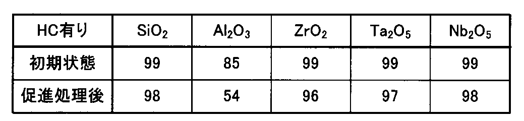
- an SiO 2 film, an Al 2 O 3 film, a ZrO 2 film, Various plastic lenses using Ta 2 O 5 film or Nb 2 O 5 film were prepared.
- Evaluation test 3 In the evaluation test 3, in the same manner as the evaluation test 1, the adhesion strength of the antireflection film and the durability (ultraviolet ray durability) of the various plastic lenses of Comparative Examples 3 and 4 were evaluated. The evaluation results are shown in Tables 4 and 5 below.
- Table 4 shows the evaluation results after 168 hours of acceleration treatment performed on the various plastic lenses of Comparative Example 3.
- Table 4 also shows the evaluation results of the plastic lens 1 of Example 1 using the base material 10 having a refractive index of 1.50 (in the column of ITO in Table 4).
- Table 5 shows the evaluation results after 168 hours of acceleration treatment performed on the various plastic lenses of Comparative Example 4.
- the antireflection film peeled off significantly after the acceleration treatment. That is, when a non-conductive SiO 2 film, Al 2 O 3 film, ZrO 2 film, Ta 2 O 5 film, and Nb 2 O 5 film are used as the adhesion layer, reflection with respect to the substrate is performed. It was found that the durability of the adhesion of the prevention film could not be obtained.
- the adhesion and durability of the interface between the base material 10 and the antireflection film 11 are improved (improved) by providing a conductive film on the surface of the antireflection film 11 on the base material 10 side. I understand.
- Patent Document 1 proposes a technique in which a metal thin film having a thickness of about 2 nm is provided as an adhesion layer at an interface between a base material and an antireflection film.
- the substance of the adhesion layer used in Patent Document 1 is a colored substance having an absorption band in visible light.
- an optical lens used for an optical system such as a camera, the influence of absorption of a visible light component in such a metal thin film can be ignored, but in a spectacle lens that is required to be transparent (colorless and transparent) with eyes, Such a colored adhesion layer cannot be used.
- the optical characteristics of the plastic lens 1 produced in Example 1 were evaluated. Specifically, the transmittance characteristic in the visible light band of the plastic lens 1 of Example 1 in which the conductive layer 13 (adhesion layer) is formed of an ITO film having a thickness of 10 nm was examined.
- the base material 10 is constituted by a substrate of refractive index 1.50
- the antireflection film body 12 was composed of a multilayer film formed by laminating seven layers and SiO 2 layers and ZrO 2 layers alternately.
- a plastic lens (Comparative Example 5) in which a Ti thin film (metal thin film) having a thickness of 2 nm was provided as an adhesion layer at the interface between the base material and the antireflection film was prepared. Similarly, the transmittance characteristic in the visible light band was examined for the plastic lens of Example 5.
- FIG. 3 shows the evaluation results of the transmittance characteristics described above.
- the characteristic shown in FIG. 3 is the transmittance spectrum in the visible light band of the plastic lens of Example 1 and Comparative Example 5, the horizontal axis indicates the wavelength, and the vertical axis indicates the true transmittance T * .
- the characteristic indicated by the thick solid line in FIG. 3 is the transmittance spectrum of the plastic lens 1 of Example 1, and the characteristic indicated by the thick broken line in FIG. 3 is the transmittance spectrum of the plastic lens of Comparative Example 5.
- the plastic lens 1 of Example 1 has a higher transmittance in the visible light band than that of Comparative Example 5. Specifically, in the plastic lens of Comparative Example 5, the average transmittance in the visible light band was 95.6%, and it was confirmed by visual observation that the lens was colored darkly. On the other hand, in the plastic lens 1 of Example 1, the transmittance average value in the visible light band was 98.8%, and high transparency was obtained. Moreover, when the transparency of the plastic lens 1 of Example 1 was confirmed by visual observation, it was confirmed that a colorless and transparent plastic lens 1 was obtained.
- the plastic lens 1 of Example 1 can not only improve (improve) the adhesion and durability of the interface between the base material 10 and the antireflection film 11, but also the colorless and transparent of the lens. It can be seen that the sex can be secured. Therefore, the plastic lens 1 of Example 1 is suitable as a spectacle lens.
- the conductive layer 13 made of a transparent conductive film the adhesion and durability of the interface between the substrate 10 and the antireflection film can be improved.
- the plastic lens 1 can be manufactured at a low cost. That is, in the embodiment (various examples), a high-quality plastic lens can be manufactured at a lower cost.
Landscapes
- Physics & Mathematics (AREA)
- General Physics & Mathematics (AREA)
- Optics & Photonics (AREA)
- Health & Medical Sciences (AREA)
- Ophthalmology & Optometry (AREA)
- Chemical & Material Sciences (AREA)
- Inorganic Chemistry (AREA)
- General Health & Medical Sciences (AREA)
- Surface Treatment Of Optical Elements (AREA)
Abstract
Description
1.プラスチックレンズの基本構成例
2.各種実施例及び評価結果
[膜剥がれの原因及びその抑制原理]
上述のように、従来の眼鏡レンズでは、プラスチック基材上に直接、反射防止膜を成膜せずに、有機樹脂に無機ゾルを分散させたハードコート層を介して、プラスチック基材上に反射防止膜を成膜する。ハードコート層を用いる理由は、上述のように、プラスチック基材及び反射防止膜間の界面の密着性及び耐久性を向上させ、プラスチックレンズの製品仕様を満たすためである。
図1に、本発明の一実施形態に係るプラスチックレンズの基本構成を示す。なお、図1は、本実施形態のプラスチックレンズの概略断面図であり、図1では、説明を簡略化するため、プラスチックレンズの一部の概略断面を示す。
次に、本実施形態において作製したプラスチックレンズ1の各種実施例の構成、及び、各種実施例のプラスチックレンズ1に対して行った密着性の評価試験について説明する。
(1)実施例1のプラスチックレンズの構成
実施例1では、屈折率の異なる種々の基材10を用いてプラスチックレンズ1を作製した。具体的には、次のようにして、実施例1の各種プラスチックレンズ1を作製した。
評価試験1では、上述のようにして作製された実施例1の各種プラスチックレンズ1における反射防止膜11の密着力及びその耐久性(紫外線耐久性)の評価を行った。具体的には、紫外線蛍光ランプ式の促進耐候試験機QUV(Q-Lab Corporation製)を用いて、上記各種プラスチックレンズ1に対して、所定時間(この例では、40時間及び168時間)の促進処理(促進耐候試験)を行い、促進処理前後の反射防止膜11の基材10に対する密着力を評価した。
上述した評価試験1の結果を下記表1に示す。表1は、屈折率の異なる各種基材10を備える各種プラスチックレンズ1の密着力の耐久性の評価結果であり、促進処理前(初期状態)、40時間の促進処理後、及び、168時間の促進処理後のクロスハッチ試験の評価結果を示す。なお、表1中の促進処理時間の各列に記載の数値は、クロスハッチ試験後に膜剥がれが生じていない部分の面積の割合(%)を示す。

ここで、上記表1に示した実施例1のプラスチックレンズ1の評価結果と比較するため、導電層を備えない反射防止膜を基材上に直接設けたプラスチックレンズ(比較例1)を作製し、その比較例1のプラスチックレンズに対しても、実施例1(評価試験1)と同様にして基材10に対する反射防止膜の密着力及びその耐久性の評価を行った。

実施例2のプラスチックレンズ1では、導電層13を、厚さ約10nmのZnOからなる透明導電膜で構成した。それ以外の構成(基材10の屈折率等)は、上記実施例1と同様である。なお、この例の導電層13の表面抵抗は約2×10⁸Ω程度であった。

評価試験3では、反射防止膜と基材との間に、ハードコートを設けた場合と、そうでない場合との密着性の差異を評価した。
上記評価を行うために、比較例3では、上記実施例1のプラスチックレンズ1(図1)において、導電層13の代わりに密着層として、SiO2膜、Al2O3膜、ZrO2膜、Ta2O5膜、又は、Nb2O5膜を用いた各種プラスチックレンズを作製した。
評価試験3では、上記評価試験1と同様にして、比較例3及び4の各種プラスチックレンズにおける反射防止膜の密着力及びその耐久性(紫外線耐久性)の評価を行った。その評価結果を、下記表4及び5に示す。

上記特許文献1では、基材及び反射防止膜間の界面に、密着層として、厚さ2nm程度の金属薄膜を設ける技術が提案されている。ただし、特許文献1で用いられている密着層の物質は可視光に吸収帯のある有色物質である。カメラ等の光学系に用いられる光学レンズでは、このような金属薄膜での可視光成分の吸収の影響は無視できるが、目で見て透明(無色透明)であることが求められる眼鏡レンズでは、このような着色した密着層は利用できない。
Claims (3)
- プラスチック基材と、
前記プラスチック基材の表面に接して形成された無色透明性を有する導電層、及び、該導電層上に形成された金属酸化物を含む反射防止膜本体を有する反射防止膜と
を備えるプラスチックレンズ。 - 前記導電層が、インジウム、スズ、亜鉛、及び、チタンのうちの少なくとも一つの元素の酸化物を含む
請求項1に記載のプラスチックレンズ。 - 前記プラスチック基材が、アリル樹脂、ウレタン樹脂、ポリスルフィド樹脂、及び、ポリカーボネート樹脂のいずれかの材料で形成される
請求項1又は2に記載のプラスチックレンズ。
Priority Applications (6)
| Application Number | Priority Date | Filing Date | Title |
|---|---|---|---|
| CN201280014502.9A CN103443663B (zh) | 2011-03-25 | 2012-03-23 | 塑料透镜 |
| US14/007,502 US9022585B2 (en) | 2011-03-25 | 2012-03-23 | Plastic lens |
| EP12763339.4A EP2690470B1 (en) | 2011-03-25 | 2012-03-23 | Plastic lens |
| JP2013507530A JPWO2012133216A1 (ja) | 2011-03-25 | 2012-03-23 | プラスチックレンズ |
| KR1020137025241A KR20140009411A (ko) | 2011-03-25 | 2012-03-23 | 플라스틱 렌즈 |
| HK14105354.3A HK1192015A1 (zh) | 2011-03-25 | 2014-06-07 | 塑料透鏡 |
Applications Claiming Priority (2)
| Application Number | Priority Date | Filing Date | Title |
|---|---|---|---|
| JP2011068611 | 2011-03-25 | ||
| JP2011-068611 | 2011-03-25 |
Publications (1)
| Publication Number | Publication Date |
|---|---|
| WO2012133216A1 true WO2012133216A1 (ja) | 2012-10-04 |
Family
ID=46930938
Family Applications (1)
| Application Number | Title | Priority Date | Filing Date |
|---|---|---|---|
| PCT/JP2012/057573 WO2012133216A1 (ja) | 2011-03-25 | 2012-03-23 | プラスチックレンズ |
Country Status (7)
| Country | Link |
|---|---|
| US (1) | US9022585B2 (ja) |
| EP (1) | EP2690470B1 (ja) |
| JP (1) | JPWO2012133216A1 (ja) |
| KR (1) | KR20140009411A (ja) |
| CN (1) | CN103443663B (ja) |
| HK (1) | HK1192015A1 (ja) |
| WO (1) | WO2012133216A1 (ja) |
Cited By (3)
| Publication number | Priority date | Publication date | Assignee | Title |
|---|---|---|---|---|
| JP2016525712A (ja) * | 2013-07-26 | 2016-08-25 | サフィーロ・ソシエタ・アツィオナリア・ファブリカ・イタリアナ・ラボラツィオーネ・オッチアリ・エス・ピー・エー | 眼鏡用の偏光レンズを製造するための方法、及び、この方法を使用して製造されたレンズ |
| WO2018155213A1 (ja) * | 2017-02-27 | 2018-08-30 | 東海光学株式会社 | プラスチック眼鏡レンズ及び眼鏡 |
| JP2022087009A (ja) * | 2020-11-30 | 2022-06-09 | デクセリアルズ株式会社 | 光学積層体、物品 |
Families Citing this family (3)
| Publication number | Priority date | Publication date | Assignee | Title |
|---|---|---|---|---|
| CN106461965B (zh) * | 2014-05-05 | 2020-01-07 | 依视路国际公司 | 包括在可见和紫外区内具有极低反射的减反射涂层的光学制品 |
| KR102038701B1 (ko) | 2018-06-22 | 2019-10-30 | 조성제 | 저강도 연속형 초음파 방식의 피부 관리장치 |
| TWI707169B (zh) | 2019-11-29 | 2020-10-11 | 大立光電股份有限公司 | 成像鏡頭、相機模組及電子裝置 |
Citations (9)
| Publication number | Priority date | Publication date | Assignee | Title |
|---|---|---|---|---|
| JPS60156001A (ja) | 1984-01-26 | 1985-08-16 | Matsushita Electric Ind Co Ltd | プラスチツク製光学部品の反射防止膜 |
| JPH06138303A (ja) | 1992-10-28 | 1994-05-20 | Olympus Optical Co Ltd | プラスチック製光学部品の反射防止膜 |
| JPH06208002A (ja) | 1991-07-11 | 1994-07-26 | Matsushita Electric Ind Co Ltd | プラスチック製光学部品の反射防止膜と その形成方法 |
| JPH1173119A (ja) * | 1997-03-24 | 1999-03-16 | Konica Corp | 電磁波シールド効果を有する反射防止コート及び反射防止コートを有する光学部材 |
| WO2001055752A1 (en) * | 2000-01-26 | 2001-08-02 | Sola International Holdings Limited | Anti-static, anti-reflection coating |
| JP2001295032A (ja) * | 2000-02-10 | 2001-10-26 | Itochu Fine Chemical Corp | 光学複合薄膜の形成方法およびそれを用いた光学物品 |
| JP2003206363A (ja) | 2002-01-10 | 2003-07-22 | Toray Ind Inc | ハードコート性を有するプラスチック成形体、およびそれからなる眼鏡用レンズ |
| JP2006138896A (ja) * | 2004-11-10 | 2006-06-01 | Seiko Epson Corp | 光学素子およびその再生方法 |
| JP2007271860A (ja) | 2006-03-31 | 2007-10-18 | Nidek Co Ltd | 反射防止膜付透明基板 |
Family Cites Families (9)
| Publication number | Priority date | Publication date | Assignee | Title |
|---|---|---|---|---|
| JP3135010B2 (ja) * | 1992-07-20 | 2001-02-13 | 富士写真光機株式会社 | 導電性反射防止膜 |
| DE69620065T2 (de) * | 1995-07-06 | 2002-11-14 | Sony Corp., Tokio/Tokyo | Elektrisch leitender, Antireflektionsbelag |
| EP0913712A1 (en) * | 1997-10-29 | 1999-05-06 | N.V. Bekaert S.A. | Multilayer electrically conductive anti-reflective coating |
| US6436541B1 (en) * | 1998-04-07 | 2002-08-20 | Ppg Industries Ohio, Inc. | Conductive antireflective coatings and methods of producing same |
| WO2001025344A1 (en) * | 1999-10-07 | 2001-04-12 | Sola International, Inc. | Uv curable coatings for plastic ophthalmic lens |
| JP3510845B2 (ja) * | 2000-08-29 | 2004-03-29 | Hoya株式会社 | 反射防止膜を有する光学部材 |
| JP2004341052A (ja) * | 2003-05-13 | 2004-12-02 | Ito Kogaku Kogyo Kk | 光学要素 |
| WO2005059600A1 (ja) | 2003-12-16 | 2005-06-30 | Murakami Corporation | 防曇素子 |
| US20080023138A1 (en) * | 2006-07-31 | 2008-01-31 | Essilor International Compagnie Generale D'optique | Process for Transferring onto a Surface of an Optical Article a Coating Stack Imparting Antistatic Properties |
-
2012
- 2012-03-23 CN CN201280014502.9A patent/CN103443663B/zh not_active Expired - Fee Related
- 2012-03-23 KR KR1020137025241A patent/KR20140009411A/ko not_active Application Discontinuation
- 2012-03-23 US US14/007,502 patent/US9022585B2/en not_active Expired - Fee Related
- 2012-03-23 JP JP2013507530A patent/JPWO2012133216A1/ja active Pending
- 2012-03-23 WO PCT/JP2012/057573 patent/WO2012133216A1/ja active Application Filing
- 2012-03-23 EP EP12763339.4A patent/EP2690470B1/en not_active Not-in-force
-
2014
- 2014-06-07 HK HK14105354.3A patent/HK1192015A1/zh not_active IP Right Cessation
Patent Citations (9)
| Publication number | Priority date | Publication date | Assignee | Title |
|---|---|---|---|---|
| JPS60156001A (ja) | 1984-01-26 | 1985-08-16 | Matsushita Electric Ind Co Ltd | プラスチツク製光学部品の反射防止膜 |
| JPH06208002A (ja) | 1991-07-11 | 1994-07-26 | Matsushita Electric Ind Co Ltd | プラスチック製光学部品の反射防止膜と その形成方法 |
| JPH06138303A (ja) | 1992-10-28 | 1994-05-20 | Olympus Optical Co Ltd | プラスチック製光学部品の反射防止膜 |
| JPH1173119A (ja) * | 1997-03-24 | 1999-03-16 | Konica Corp | 電磁波シールド効果を有する反射防止コート及び反射防止コートを有する光学部材 |
| WO2001055752A1 (en) * | 2000-01-26 | 2001-08-02 | Sola International Holdings Limited | Anti-static, anti-reflection coating |
| JP2001295032A (ja) * | 2000-02-10 | 2001-10-26 | Itochu Fine Chemical Corp | 光学複合薄膜の形成方法およびそれを用いた光学物品 |
| JP2003206363A (ja) | 2002-01-10 | 2003-07-22 | Toray Ind Inc | ハードコート性を有するプラスチック成形体、およびそれからなる眼鏡用レンズ |
| JP2006138896A (ja) * | 2004-11-10 | 2006-06-01 | Seiko Epson Corp | 光学素子およびその再生方法 |
| JP2007271860A (ja) | 2006-03-31 | 2007-10-18 | Nidek Co Ltd | 反射防止膜付透明基板 |
Non-Patent Citations (1)
| Title |
|---|
| See also references of EP2690470A4 * |
Cited By (5)
| Publication number | Priority date | Publication date | Assignee | Title |
|---|---|---|---|---|
| JP2016525712A (ja) * | 2013-07-26 | 2016-08-25 | サフィーロ・ソシエタ・アツィオナリア・ファブリカ・イタリアナ・ラボラツィオーネ・オッチアリ・エス・ピー・エー | 眼鏡用の偏光レンズを製造するための方法、及び、この方法を使用して製造されたレンズ |
| WO2018155213A1 (ja) * | 2017-02-27 | 2018-08-30 | 東海光学株式会社 | プラスチック眼鏡レンズ及び眼鏡 |
| JP2018141847A (ja) * | 2017-02-27 | 2018-09-13 | 東海光学株式会社 | プラスチック眼鏡レンズ及び眼鏡 |
| US11422287B2 (en) | 2017-02-27 | 2022-08-23 | Tokai Optical Co., Ltd. | Plastic spectacle lens and spectacles |
| JP2022087009A (ja) * | 2020-11-30 | 2022-06-09 | デクセリアルズ株式会社 | 光学積層体、物品 |
Also Published As
| Publication number | Publication date |
|---|---|
| HK1192015A1 (zh) | 2014-08-08 |
| EP2690470A4 (en) | 2014-08-27 |
| US20140063608A1 (en) | 2014-03-06 |
| CN103443663B (zh) | 2016-03-23 |
| CN103443663A (zh) | 2013-12-11 |
| JPWO2012133216A1 (ja) | 2014-07-28 |
| EP2690470B1 (en) | 2016-03-16 |
| KR20140009411A (ko) | 2014-01-22 |
| EP2690470A1 (en) | 2014-01-29 |
| US9022585B2 (en) | 2015-05-05 |
Similar Documents
| Publication | Publication Date | Title |
|---|---|---|
| WO2012133216A1 (ja) | プラスチックレンズ | |
| KR102618675B1 (ko) | 안경 렌즈 | |
| CN103329013B (zh) | 包括在紫外区和可见光区中具有低反射的抗反射涂层的光学制品 | |
| KR101800495B1 (ko) | 투명 도전성 필름 및 터치 패널 | |
| JP4966924B2 (ja) | 透明導電性フィルム、透明導電性積層体及びタッチパネル、並びに透明導電性フィルムの製造方法 | |
| EP3203274B1 (en) | Ophthalmic lens comprising a thin antireflective coating with a very low reflection in the visible | |
| KR101638278B1 (ko) | 투명 도전성 필름 및 터치 패널 | |
| JP2012032690A (ja) | 光学物品およびその製造方法 | |
| EA017400B1 (ru) | Элемент остекления и его применение | |
| JP2009128820A (ja) | 多層反射防止膜を有するプラスチックレンズおよびその製造方法 | |
| TWI483270B (zh) | 電特性優秀的透明導電性膜及利用該透明導電性膜的觸控面板 | |
| JP5523066B2 (ja) | 光学物品の製造方法 | |
| JP4349794B2 (ja) | 導電性を有する多層反射防止膜付透明基板の製造方法 | |
| KR20170047371A (ko) | 적외선 흡수층을 포함하는 광학 필름 | |
| JP2010231174A (ja) | 光学物品およびその製造方法 | |
| AU2016240877B2 (en) | Spectacle lens, method of manufacturing the same, and spectacles | |
| US8736945B2 (en) | Lens module with infrared absorbing filter | |
| JP2005047178A (ja) | 導電性を有する多層膜付透明基板 | |
| JP5973195B2 (ja) | プラスチックレンズ | |
| JP5859598B2 (ja) | 透明導電性フィルム及びタッチパネル | |
| ES2354351A1 (es) | Lente oftálmica y/o solar y procedimiento de fabricación correspondiente. | |
| US7785714B2 (en) | Extreme low resistivity light attenuation anti-reflection coating structure and method for manufacturing the same | |
| JP2016177940A (ja) | 透明導電体の製造方法 | |
| JP5859597B2 (ja) | 透明導電性フィルム及びタッチパネル | |
| JP2016160115A (ja) | 透明導電部材の選別方法 |
Legal Events
| Date | Code | Title | Description |
|---|---|---|---|
| WWE | Wipo information: entry into national phase |
Ref document number: 201280014502.9 Country of ref document: CN |
|
| 121 | Ep: the epo has been informed by wipo that ep was designated in this application |
Ref document number: 12763339 Country of ref document: EP Kind code of ref document: A1 |
|
| ENP | Entry into the national phase |
Ref document number: 2013507530 Country of ref document: JP Kind code of ref document: A |
|
| WWE | Wipo information: entry into national phase |
Ref document number: 2012763339 Country of ref document: EP |
|
| ENP | Entry into the national phase |
Ref document number: 20137025241 Country of ref document: KR Kind code of ref document: A |
|
| NENP | Non-entry into the national phase |
Ref country code: DE |
|
| WWE | Wipo information: entry into national phase |
Ref document number: 14007502 Country of ref document: US |