WO2012128051A1 - 透明導電膜の製造方法および太陽電池の製造方法 - Google Patents
透明導電膜の製造方法および太陽電池の製造方法 Download PDFInfo
- Publication number
- WO2012128051A1 WO2012128051A1 PCT/JP2012/055906 JP2012055906W WO2012128051A1 WO 2012128051 A1 WO2012128051 A1 WO 2012128051A1 JP 2012055906 W JP2012055906 W JP 2012055906W WO 2012128051 A1 WO2012128051 A1 WO 2012128051A1
- Authority
- WO
- WIPO (PCT)
- Prior art keywords
- transparent conductive
- conductive film
- substrate
- metal plate
- solar cell
- Prior art date
- Legal status (The legal status is an assumption and is not a legal conclusion. Google has not performed a legal analysis and makes no representation as to the accuracy of the status listed.)
- Ceased
Links
Images
Classifications
-
- H—ELECTRICITY
- H10—SEMICONDUCTOR DEVICES; ELECTRIC SOLID-STATE DEVICES NOT OTHERWISE PROVIDED FOR
- H10F—INORGANIC SEMICONDUCTOR DEVICES SENSITIVE TO INFRARED RADIATION, LIGHT, ELECTROMAGNETIC RADIATION OF SHORTER WAVELENGTH OR CORPUSCULAR RADIATION
- H10F77/00—Constructional details of devices covered by this subclass
- H10F77/20—Electrodes
- H10F77/244—Electrodes made of transparent conductive layers, e.g. transparent conductive oxide [TCO] layers
-
- C—CHEMISTRY; METALLURGY
- C23—COATING METALLIC MATERIAL; COATING MATERIAL WITH METALLIC MATERIAL; CHEMICAL SURFACE TREATMENT; DIFFUSION TREATMENT OF METALLIC MATERIAL; COATING BY VACUUM EVAPORATION, BY SPUTTERING, BY ION IMPLANTATION OR BY CHEMICAL VAPOUR DEPOSITION, IN GENERAL; INHIBITING CORROSION OF METALLIC MATERIAL OR INCRUSTATION IN GENERAL
- C23C—COATING METALLIC MATERIAL; COATING MATERIAL WITH METALLIC MATERIAL; SURFACE TREATMENT OF METALLIC MATERIAL BY DIFFUSION INTO THE SURFACE, BY CHEMICAL CONVERSION OR SUBSTITUTION; COATING BY VACUUM EVAPORATION, BY SPUTTERING, BY ION IMPLANTATION OR BY CHEMICAL VAPOUR DEPOSITION, IN GENERAL
- C23C14/00—Coating by vacuum evaporation, by sputtering or by ion implantation of the coating forming material
- C23C14/0015—Coating by vacuum evaporation, by sputtering or by ion implantation of the coating forming material characterized by the colour of the layer
-
- C—CHEMISTRY; METALLURGY
- C23—COATING METALLIC MATERIAL; COATING MATERIAL WITH METALLIC MATERIAL; CHEMICAL SURFACE TREATMENT; DIFFUSION TREATMENT OF METALLIC MATERIAL; COATING BY VACUUM EVAPORATION, BY SPUTTERING, BY ION IMPLANTATION OR BY CHEMICAL VAPOUR DEPOSITION, IN GENERAL; INHIBITING CORROSION OF METALLIC MATERIAL OR INCRUSTATION IN GENERAL
- C23C—COATING METALLIC MATERIAL; COATING MATERIAL WITH METALLIC MATERIAL; SURFACE TREATMENT OF METALLIC MATERIAL BY DIFFUSION INTO THE SURFACE, BY CHEMICAL CONVERSION OR SUBSTITUTION; COATING BY VACUUM EVAPORATION, BY SPUTTERING, BY ION IMPLANTATION OR BY CHEMICAL VAPOUR DEPOSITION, IN GENERAL
- C23C14/00—Coating by vacuum evaporation, by sputtering or by ion implantation of the coating forming material
- C23C14/06—Coating by vacuum evaporation, by sputtering or by ion implantation of the coating forming material characterised by the coating material
- C23C14/14—Metallic material, boron or silicon
-
- C—CHEMISTRY; METALLURGY
- C23—COATING METALLIC MATERIAL; COATING MATERIAL WITH METALLIC MATERIAL; CHEMICAL SURFACE TREATMENT; DIFFUSION TREATMENT OF METALLIC MATERIAL; COATING BY VACUUM EVAPORATION, BY SPUTTERING, BY ION IMPLANTATION OR BY CHEMICAL VAPOUR DEPOSITION, IN GENERAL; INHIBITING CORROSION OF METALLIC MATERIAL OR INCRUSTATION IN GENERAL
- C23C—COATING METALLIC MATERIAL; COATING MATERIAL WITH METALLIC MATERIAL; SURFACE TREATMENT OF METALLIC MATERIAL BY DIFFUSION INTO THE SURFACE, BY CHEMICAL CONVERSION OR SUBSTITUTION; COATING BY VACUUM EVAPORATION, BY SPUTTERING, BY ION IMPLANTATION OR BY CHEMICAL VAPOUR DEPOSITION, IN GENERAL
- C23C14/00—Coating by vacuum evaporation, by sputtering or by ion implantation of the coating forming material
- C23C14/22—Coating by vacuum evaporation, by sputtering or by ion implantation of the coating forming material characterised by the process of coating
- C23C14/24—Vacuum evaporation
-
- C—CHEMISTRY; METALLURGY
- C23—COATING METALLIC MATERIAL; COATING MATERIAL WITH METALLIC MATERIAL; CHEMICAL SURFACE TREATMENT; DIFFUSION TREATMENT OF METALLIC MATERIAL; COATING BY VACUUM EVAPORATION, BY SPUTTERING, BY ION IMPLANTATION OR BY CHEMICAL VAPOUR DEPOSITION, IN GENERAL; INHIBITING CORROSION OF METALLIC MATERIAL OR INCRUSTATION IN GENERAL
- C23C—COATING METALLIC MATERIAL; COATING MATERIAL WITH METALLIC MATERIAL; SURFACE TREATMENT OF METALLIC MATERIAL BY DIFFUSION INTO THE SURFACE, BY CHEMICAL CONVERSION OR SUBSTITUTION; COATING BY VACUUM EVAPORATION, BY SPUTTERING, BY ION IMPLANTATION OR BY CHEMICAL VAPOUR DEPOSITION, IN GENERAL
- C23C14/00—Coating by vacuum evaporation, by sputtering or by ion implantation of the coating forming material
- C23C14/22—Coating by vacuum evaporation, by sputtering or by ion implantation of the coating forming material characterised by the process of coating
- C23C14/56—Apparatus specially adapted for continuous coating; Arrangements for maintaining the vacuum, e.g. vacuum locks
-
- C—CHEMISTRY; METALLURGY
- C23—COATING METALLIC MATERIAL; COATING MATERIAL WITH METALLIC MATERIAL; CHEMICAL SURFACE TREATMENT; DIFFUSION TREATMENT OF METALLIC MATERIAL; COATING BY VACUUM EVAPORATION, BY SPUTTERING, BY ION IMPLANTATION OR BY CHEMICAL VAPOUR DEPOSITION, IN GENERAL; INHIBITING CORROSION OF METALLIC MATERIAL OR INCRUSTATION IN GENERAL
- C23C—COATING METALLIC MATERIAL; COATING MATERIAL WITH METALLIC MATERIAL; SURFACE TREATMENT OF METALLIC MATERIAL BY DIFFUSION INTO THE SURFACE, BY CHEMICAL CONVERSION OR SUBSTITUTION; COATING BY VACUUM EVAPORATION, BY SPUTTERING, BY ION IMPLANTATION OR BY CHEMICAL VAPOUR DEPOSITION, IN GENERAL
- C23C14/00—Coating by vacuum evaporation, by sputtering or by ion implantation of the coating forming material
- C23C14/58—After-treatment
- C23C14/5806—Thermal treatment
-
- H—ELECTRICITY
- H10—SEMICONDUCTOR DEVICES; ELECTRIC SOLID-STATE DEVICES NOT OTHERWISE PROVIDED FOR
- H10F—INORGANIC SEMICONDUCTOR DEVICES SENSITIVE TO INFRARED RADIATION, LIGHT, ELECTROMAGNETIC RADIATION OF SHORTER WAVELENGTH OR CORPUSCULAR RADIATION
- H10F10/00—Individual photovoltaic cells, e.g. solar cells
- H10F10/10—Individual photovoltaic cells, e.g. solar cells having potential barriers
- H10F10/16—Photovoltaic cells having only PN heterojunction potential barriers
- H10F10/164—Photovoltaic cells having only PN heterojunction potential barriers comprising heterojunctions with Group IV materials, e.g. ITO/Si or GaAs/SiGe photovoltaic cells
- H10F10/165—Photovoltaic cells having only PN heterojunction potential barriers comprising heterojunctions with Group IV materials, e.g. ITO/Si or GaAs/SiGe photovoltaic cells the heterojunctions being Group IV-IV heterojunctions, e.g. Si/Ge, SiGe/Si or Si/SiC photovoltaic cells
- H10F10/166—Photovoltaic cells having only PN heterojunction potential barriers comprising heterojunctions with Group IV materials, e.g. ITO/Si or GaAs/SiGe photovoltaic cells the heterojunctions being Group IV-IV heterojunctions, e.g. Si/Ge, SiGe/Si or Si/SiC photovoltaic cells the Group IV-IV heterojunctions being heterojunctions of crystalline and amorphous materials, e.g. silicon heterojunction [SHJ] photovoltaic cells
-
- H—ELECTRICITY
- H10—SEMICONDUCTOR DEVICES; ELECTRIC SOLID-STATE DEVICES NOT OTHERWISE PROVIDED FOR
- H10F—INORGANIC SEMICONDUCTOR DEVICES SENSITIVE TO INFRARED RADIATION, LIGHT, ELECTROMAGNETIC RADIATION OF SHORTER WAVELENGTH OR CORPUSCULAR RADIATION
- H10F71/00—Manufacture or treatment of devices covered by this subclass
- H10F71/138—Manufacture of transparent electrodes, e.g. transparent conductive oxides [TCO] or indium tin oxide [ITO] electrodes
-
- Y—GENERAL TAGGING OF NEW TECHNOLOGICAL DEVELOPMENTS; GENERAL TAGGING OF CROSS-SECTIONAL TECHNOLOGIES SPANNING OVER SEVERAL SECTIONS OF THE IPC; TECHNICAL SUBJECTS COVERED BY FORMER USPC CROSS-REFERENCE ART COLLECTIONS [XRACs] AND DIGESTS
- Y02—TECHNOLOGIES OR APPLICATIONS FOR MITIGATION OR ADAPTATION AGAINST CLIMATE CHANGE
- Y02E—REDUCTION OF GREENHOUSE GAS [GHG] EMISSIONS, RELATED TO ENERGY GENERATION, TRANSMISSION OR DISTRIBUTION
- Y02E10/00—Energy generation through renewable energy sources
- Y02E10/50—Photovoltaic [PV] energy
Definitions
- the present invention relates to a method for producing a transparent conductive film and a method for producing a solar cell.
- Transparent conductive films made of translucent conductive oxides such as indium oxide films and zinc oxide are used as electrodes for various devices such as solar cells and liquid crystal panels.
- Patent Document 1 discloses a method for improving the crystallinity of an indium oxide film by irradiating a substrate on which an indium oxide film is formed with infrared rays through a tube using an infrared lamp.
- Patent Document 1 after an indium oxide film is formed on a substrate, the substrate is taken out from the film formation apparatus, and the indium oxide film is irradiated with infrared rays using an infrared lamp.
- the indium oxide film is exposed to air or the like. For this reason, the surface of the indium oxide film may be oxidized or other impurities may adhere to the surface of the indium oxide film. Even if the film is modified by irradiating infrared rays, the modification is hindered by the surface impurities. There is a risk.
- an object of the present invention is to provide a transparent conductive film with few crystal grain boundaries by satisfactorily modifying the transparent conductive film.
- the transparent conductive film of the present invention after forming a transparent conductive film on a substrate in a vacuum vessel, the transparent conductive film is modified without being exposed to the atmosphere.
- the substrate is not exposed to the atmosphere until the modification of the transparent conductive film is completed, so that the surface of the transparent conductive film is not oxidized and other impurities are not attached to the surface. Quality processing is possible.
- the transparent conductive film used in the embodiment is made of a light-transmitting conductive oxide such as indium oxide, zinc oxide, or tin oxide. These translucent conductive oxides contain a dopant.
- the dopant is selected from tin, tungsten, cerium, zirconium, hafnium, titanium, niobium, and the like.
- the transparent conductive film is made of zinc oxide, the dopant is selected from aluminum, gallium, indium, boron and the like.
- the transparent conductive film is made of tin oxide, the dopant is selected from fluorine, antimony, and the like.
- the method for forming the transparent conductive film used in the present invention is not particularly limited, and specifically, vacuum deposition methods (electron beam type, resistance heating type, high frequency induction type, laser type, etc.), ion plating method, It is selected from sputtering or chemical vapor deposition (CVD).
- vacuum deposition methods electron beam type, resistance heating type, high frequency induction type, laser type, etc.
- ion plating method It is selected from sputtering or chemical vapor deposition (CVD).
- the transparent conductive film is modified without being exposed to the atmosphere.
- the substrate is not exposed to the atmosphere until the modification process is completed.
- the vacuum container for film formation and the surface reforming apparatus for the modification treatment may be in the same vacuum container or different vacuum containers, but the substrate is kept in the atmosphere until the modification treatment is completed. Is configured not to be exposed.
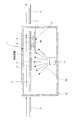
- the film forming apparatus 1 includes a vacuum container 10 and a material source 11 in the vacuum container 10.
- the substrate 2 is transferred to the vacuum container 10 in the direction of the arrow in the figure.
- the film-forming seed 3 a emitted from the material source 11 adheres, and the transparent conductive film 3 containing a light-transmitting conductive oxide such as indium oxide as a component is formed on the surface of the substrate 2. .
- the material source 11 is disposed so as to face the substrate 2 to be transported.
- a raw material such as indium oxide is accommodated in a crucible.
- Energy of electron beam irradiation, resistance heating, high frequency induction heating, laser irradiation, ion irradiation, or the like is applied to the raw material of the material source 11, and the film-forming species 3a is directed from the material source 11 toward the substrate 2 as indicated by an arrow in the figure. Is released as follows. Then, the film formation seed 3a adheres to the surface of the substrate 2, and the transparent conductive film 3 is formed.
- the vacuum vessel 10 is evacuated from a not-shown exhaust port by a not-shown vacuum pump and maintained at a predetermined degree of vacuum.
- an atmospheric gas such as Ar gas is supplied to the vacuum vessel 10.
- the supply of the atmospheric gas is controlled by a mass flow controller (not shown).
- the mass flow controller can be provided according to a method of applying energy to the raw material.
- a cooling means (not shown) is provided around the outer wall of the vacuum vessel 10, and the outer wall temperature of the vacuum vessel 10 is controlled to be about 50 ° C.
- the substrate 2 is carried into the vacuum vessel 10, and the transparent conductive film 3 is formed on the surface of the substrate 2 while the substrate 2 is being transported. Then, as will be described later, the transparent conductive film 3 formed in the vacuum container 10 is modified by applying radiant heat, and after the transparent conductive film 3 is modified, the substrate 2 is taken out of the vacuum container 10 and the atmosphere It is configured to be exposed inside.
- a surface reformer 4 for providing heat in the vicinity of the substrate 2 on which the transparent conductive film 3 is formed is provided in the vacuum vessel 1.
- the surface modification device 4 is configured to apply heat to the transparent conductive film 3 immediately after film formation.
- the surface modification device 4 is composed of a metal plate 40 made of a stainless steel plate (SUS) or a copper plate (Cu), and is arranged on the wall surface of the vacuum vessel 10 in parallel and close to the substrate 2 to be transported.
- the metal plate 40 constituting the surface modification device 4 is heated by the radiant heat from the material source 11 and is configured to have a temperature of 150 ° C. to 400 ° C. Electromagnetic waves are radiated from the heated metal plate 40 to the surface of the transparent conductive film 3 of the substrate 2, and the transparent conductive film 3 is heated.
- the grain size of the transparent conductive film 3 immediately after film formation is enlarged, the crystal grain boundary is reduced, and the transparent conductive film 3 is modified. Further, since the transparent conductive film 3 is not exposed to the atmosphere until the modification of the transparent conductive film 3 is completed, there is no possibility that the surface of the transparent conductive film 3 is oxidized or other impurities are attached to the surface. Can be processed.
- the electromagnetic wave emitted from the surface modification device 4 selectively heats the transparent conductive film 3 formed on the surface of the substrate 2 without affecting the substrate 2 itself. It is preferably not absorbed by devices other than the transparent conductive film 3 formed on the substrate 2.
- the substrate 2 after the transparent conductive film 3 is formed is shielded from the material source 11 by the surface modification device 4, the substrate 2 is suppressed from being heated by the radiant heat from the material source 11. Therefore, even if the substrate 2 has a semiconductor junction made of amorphous silicon, the modification process of the transparent conductive film 3 can be performed without damaging the semiconductor junction of the substrate.
- the transparent conductive film 3 is formed on the substrate 2 by the sputtering method
- the raw material target is held in the material source 11.
- the raw material target is sputtered, and the film formation seed 3 a reaches the surface of the substrate 2 to form a film.
- the metal plate 40 of the surface modification device 4 is heated by plasma heat or the like generated during the film formation. Electromagnetic waves are radiated from the heated metal plate 40 to the surface of the transparent conductive film 3 of the substrate 2, and the transparent conductive film 3 is heated.
- the grain size of the transparent conductive film 3 immediately after film formation is enlarged, the crystal grain boundary is reduced, and the transparent conductive film 3 is modified.
- the transparent conductive film produced according to the embodiment can be used as a transparent electrode in a solar cell.
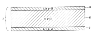
- the structure of the solar cell which has the transparent conductive film formed by the manufacturing method of embodiment is shown in FIG.
- the solar cell shown in FIG. 2 has a structure in which an intrinsic amorphous silicon layer is interposed between a single crystal silicon substrate 20 and an amorphous silicon layer 22 having opposite conductivity types. With such a configuration, defects at the interface between the crystalline silicon substrate and the amorphous silicon layer are reduced, and the characteristics of the heterojunction interface are improved.
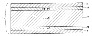
- FIG. 3 is a schematic cross-sectional view showing the solar cell having the above-described structure.
- an intrinsic (i-type) amorphous silicon layer and a p-type amorphous layer are formed on one main surface of an n-type crystalline silicon (nc-Si) substrate 20 made of a single crystal silicon semiconductor.
- Silicon layers (i / p a-Si) 22 are stacked in this order.
- a transparent conductive film 3 made of indium oxide to which tin is added and a comb-shaped collector electrode (not shown) made of silver (Ag) are formed.
- an i-type amorphous silicon layer and an n-type amorphous silicon layer (n / i a-Si) 21 are stacked in this order. Further thereon, a transparent conductive film 3 and a comb-shaped collector electrode (not shown) are formed.
- the above-mentioned transparent conductive film 3 of the solar cell is required to have a film with few crystal grain boundaries in order to improve performance and reliability. Specifically, the transparent conductive film 3 is required to increase resistance to sodium contained in the solar cell module. If the transparent conductive film 3 is formed on the above-described solar cell by the manufacturing method of the embodiment, the performance and the reliability can be improved. That is, the transparent conductive film 3 formed on the amorphous silicon layer 21 or 22 is modified by the radiant heat applied from the surface modifying device 4, and performance and reliability can be improved.
- the film forming method of the embodiment is preferably modified by selectively applying radiant heat to the transparent conductive film 3 without affecting the semiconductor junction by the amorphous silicon film formed on the crystalline silicon substrate 20.
- the surface modification device 4 is formed to emit electromagnetic waves in a wavelength region that is not absorbed by the amorphous silicon film. If the temperature of the metal plate of the surface modification device 4 becomes too high, the visible light component (wavelength 0.4 to 0.6 ⁇ m) increases, so that it becomes visible (red heat). Since electromagnetic waves in this wavelength region are absorbed by amorphous silicon, there is a possibility of adversely affecting the semiconductor junction.
- the metal plate 40 of the surface modification device 4 is heated so as to be 160 ° C. or higher and 400 ° C. or lower.
- the peak wavelength of the radiated electromagnetic wave from the metal plate 40 of the surface modification device 4 is 6.69 ⁇ m at 160 ° C., 4.65 ⁇ m at 350 ° C., 4.31 ⁇ m at 400 ° C. It is.
- the transparent conductive film 3 is modified without heating amorphous silicon by heating the crystalline silicon substrate 20 on which the transparent conductive film 3 is formed by radiant heat from the metal plate 40 heated to these temperatures. be able to.
- the transparent conductive film 3 is modified by using the metal plate of the surface modification device 4 and the metal plate 40 of the surface modification device 4 is not used.
- the characteristics of the provided ones were compared.
- the metal plate 40 of the surface modification device 4 was set to a temperature of 150 ° C., and the radiant heat was applied to the transparent conductive film 3.
- Table 1 shows the measured values normalized with the values of the sample without the metal plate.
- a transparent conductive film 3 made of an indium oxide film was formed by sputtering on a substantially square solar cell with a side of 104 mm.
- the maximum output Pmax was improved by 2.6% by heating the transparent conductive film 3 with the metal plate 40 of the surface modification device 4.
- Short circuit current (Isc) and fill factor (FF) are mainly improved, and the crystallinity is improved and the activation rate of the dopant is increased by performing a modification treatment by heating immediately after the transparent conductive film 3 is formed. This is considered to be due to a decrease in resistivity of the transparent conductive film.
- the reliability test results of the transparent conductive film 3 formed by changing the temperature of the metal plate 40 of the surface modification device 4 of the embodiment are shown in Table 2. Shown in A sample in which radiant heat at a temperature of 150 ° C. was applied to the transparent conductive film 3 and a sample in which radiant heat at a temperature of 350 ° C. was applied to the transparent conductive film 3 were prepared. In the sample, a transparent conductive film 3 made of an indium oxide film was formed on a substantially square solar cell with a side of 125 mm by a sputtering method.
- the produced solar cell was sealed between a glass plate and a PET sheet using an EVA sheet to produce a measurement sample.
- This sample was tested for 1000 hours in an atmosphere of 85 ° C. and 85%, and the ratio of the maximum output Pmax after the test to the maximum output Pmax before the test was determined.
- the results in Table 2 show the ratio between the minimum value (min.) And the average value (Ave.) of the maximum output Pmax.
- the electromagnetic wave to be applied preferably has a peak wavelength of 1200 nm, preferably 1500 nm, and more preferably a peak wavelength of 4 ⁇ m or more.
- the surface modification device 4 in the above-described embodiment is configured by the metal plate 40 disposed close to the substrate 2 and heated by the radiant heat from the material source 11, an apparatus for heating the metal plate 40 is provided. There is no need to provide it, and the apparatus can be simplified.
- the surface modification device 4 is not limited to the above configuration, and is a device different from the material source 11 and uses a device that radiates far infrared rays by setting the surface modification device 4 to a predetermined temperature. Is also possible. For example, a far infrared lamp can be used.
- the vapor deposition source 11 and the surface modification device 4 are provided in the same container.
- the film formation and the modification may be performed in different containers. Even in this case, the substrate 2 is configured not to be exposed to the atmosphere until the modification process of the transparent conductive film 3 is completed.
Landscapes
- Chemical & Material Sciences (AREA)
- Engineering & Computer Science (AREA)
- Organic Chemistry (AREA)
- Materials Engineering (AREA)
- Mechanical Engineering (AREA)
- Metallurgy (AREA)
- Chemical Kinetics & Catalysis (AREA)
- Physics & Mathematics (AREA)
- Thermal Sciences (AREA)
- Photovoltaic Devices (AREA)
- Physical Vapour Deposition (AREA)
- Manufacturing Of Electric Cables (AREA)
- Life Sciences & Earth Sciences (AREA)
- Sustainable Energy (AREA)
Abstract
この発明は、透明導電膜の改質を良好に行い、結晶粒界の少ない透明導電膜を提供することを目的とする。この発明の明導電膜の製造方法は、真空容器10内で基板2上に透明導電膜3を成膜した後、基板2に近接して配置された表面改質装置4から輻射熱を与え、透明導電膜3を改質し、改質された透明導電膜3を有する基板2を真空容器10より取り出す。
Description
この発明は、透明導電膜の製造方法および太陽電池の製造方法に関するものである。
酸化インジウム膜や酸化亜鉛などの透光性導電酸化物からなる透明導電膜が太陽電池、液晶パネル等の各種デバイスの電極として用いられている。
これら透明導電膜の性能向上、低抵抗化を行う方法が種々提案されている。例えば、特許文献1には、酸化インジウム膜が形成された基板を、赤外線ランプを用いてチューブ越しに赤外線を照射し、酸化インジウム膜の結晶性を向上させる方法が開示されている。
上記した特許文献1のものは、酸化インジウム膜を基板上に形成した後、基板を成膜装置から取り出し、赤外線ランプを用いて酸化インジウム膜に赤外線を照射している。この方法では、酸化インジウム膜を成膜した後、酸化インジウム膜が空気中等に暴露される。このため、酸化インジウム膜表面が酸化したり、酸化インジウム膜表面に他の不純物が付着する虞があり、赤外線を照射して膜の改質を行っても表面の不純物などにより改質が阻害される虞がある。
この発明は、上記点に鑑み、透明導電膜の改質を良好に行い、結晶粒界の少ない透明導電膜を提供することを目的とする。
この発明の透明導電膜の製造方法は、真空容器内で基板上に透明導電膜を成膜した後、大気に曝すことなく透明導電膜の改質処理をする。
この発明は、透明導電膜の改質処理が完了するまで、基板を大気中には暴露しないので、透明導電膜表面が酸化したり、表面に他の不純物が付着する虞がなく、良好な改質処理が行える。
実施形態について図面を参照しながら詳細に説明する。なお、図中同一または相当部分には同一符号を付し、説明の重複を避けるためにその説明は繰返さない。
実施形態に用いられる透明導電膜は、酸化インジウム、酸化亜鉛、酸化錫等の透光性導電酸化物からなる。これらの透光性導電酸化物は、ドーパントを含有する。透明導電膜が酸化インジウムからなる場合、ドーパントは錫、タングステン、セリウム、ジルコニウム、ハフニウム、チタン或いはニオブ等から選択される。透明導電膜が酸化亜鉛からなる場合、ドーパントはアルミニウム、ガリウム、インジウム、ボロン等から選択される。透明導電膜が酸化錫からなる場合、ドーパントはフッ素やアンチモン等から選択される。
この発明に用いられる透明導電膜の成膜方法は、特に限定されないが、具体的には、真空蒸着法(電子ビーム式、抵抗加熱式、高周波誘導式、レーザー式等)、イオンプレーティング法、スパッタ法または化学的気相成長法(CVD法)等から選択される。
実施形態の成膜方法は、真空容器内で基板上に透明導電膜を成膜した後、大気に曝すことなく透明導電膜を改質する。改質処理が終わるまで、基板を大気中には暴露しない。成膜を行う真空容器と改質処理を行う表面改質装置は、同一真空容器内であっても、それぞれ別の真空容器であっても良いが、改質処理が終わるまで基板を大気中には暴露しないように構成される。
以下、実施形態につき、図1を参照して説明する。成膜装置1は真空容器10を備え、真空容器10内には材料源11を備える。真空容器10に基板2が図中矢印方向に搬送される。基板2の搬送中に、材料源11から放出された成膜種3aが付着し、基板2表面に酸化インジウム等の透光性導電酸化物を構成成分とする透明導電膜3が成膜される。
材料源11は、搬送される基板2に対向して配置され、例えば、坩堝内に酸化インジウムなどの原料が収容される。材料源11の原料に、電子ビーム照射、抵抗加熱、高周波誘導加熱、レーザー照射、イオン照射などのエネルギーが付与され、成膜種3aが材料源11から基板2に向かって、図中矢印に示すように放出される。そして、成膜種3aは、基板2の表面に付着し、透明導電膜3が成膜される。
真空容器10は、図示しない排気口から図示しない真空ポンプにより排気され、所定の真空度に維持される。また、真空容器10には、Arガスなどの雰囲気ガスが供給される。雰囲気ガスの供給は図示しないマスフローコントローラによって制御される。マスフローコントローラは、原料にエネルギーを付与する方法に応じて設けることができる。
また、真空容器10の外壁周囲には、図示しない冷却手段が備えられ、真空容器10の外壁温度は50℃程度になるように制御される。
この実施形態においては、図1に示されるように、基板2が真空容器10内に搬入され、基板2が搬送されながら基板2の表面上に透明導電膜3が成膜される。そして、後述するように、真空容器10内で成膜された透明導電膜3に輻射熱を与えて改質し、透明導電膜3が改質された後に、基板2を真空容器10より取り出し、大気中に暴露するように構成している。
図1に示されるように、真空容器1内には、透明導電膜3が形成された基板2に近接して熱を与える表面改質装置4が設けられている。この表面改質装置4は、成膜直後の透明導電膜3に熱が与えられるように構成されている。
この実施形態において、材料源11中の原料は、加熱され蒸発して成膜種3aとなる。表面改質装置4は、ステンレス鋼板(SUS)や銅板(Cu)からなる金属板40で構成され、真空容器10の壁面に、搬送される基板2に平行に近接して配置される。表面改質装置4を構成する金属板40は、材料源11からの輻射熱により加熱され、温度が150℃~400℃になるように構成される。加熱された金属板40から電磁波が基板2の透明導電膜3の表面に輻射され、透明導電膜3が加熱される。その結果、成膜直後の透明導電膜3の粒径が拡大し、結晶粒界が低減して、透明導電膜3が改質される。また、透明導電膜3の改質処理が完了するまで基板2大気中に暴露されないので、透明導電膜3の表面が酸化したり、表面に他の不純物が付着する虞がなく、良好な改質処理が行える。
表面改質装置4から放出される電磁波は、基板2自体には影響を及ばさずに、基板2表面に形成された透明導電膜3を選択的に加熱するものとすることが好ましい。基板2に形成された透明導電膜3以外のデバイス等には吸収されないものとすることが好ましい。
透明導電膜3が成膜された後の基板2は表面改質装置4により材料源11から遮蔽されているので、基板2は、材料源11からの輻射熱によって加熱されることが抑制される。従って、基板2が非晶質シリコンによる半導体接合を有するものであっても、基板の半導体接合にダメージを与えることなく、透明導電膜3の改質処理が行える。
また、スパッタ法により基板2上に透明導電膜3を成膜する際には、材料源11に原料ターゲットが保持される。そして、イオンやラジカルが原料ターゲットに照射されることにより、原料ターゲットがスパッタされ、成膜種3aが基板2の表面に到達して成膜される。この成膜中に発生するプラズマ熱等により表面改質装置4の金属板40が加熱される。加熱された金属板40から電磁波が基板2の透明導電膜3の表面に輻射され、透明導電膜3が加熱される。その結果、成膜直後の透明導電膜3の粒径が拡大し、結晶粒界が低減して、透明導電膜3が改質される。
実施形態により製造される透明導電膜は、太陽電池に透明電極として用いることができる。実施形態の製造方法により形成された透明導電膜を有する太陽電池の構成を図2に示す。図2に示す太陽電池は、互いに逆導電型を有する単結晶シリコン基板20と非晶質シリコン層22との間に真性な非晶質シリコン層を介挿した構造を有する。このような構成とすることによって、結晶シリコン基板と非晶質シリコン層との界面での欠陥が低減し、ヘテロ接合界面の特性が改善される。
図3は、上記した構造の太陽電池を示す模式的断面図である。図3において、単結晶シリコン半導体からなるn型の結晶シリコン(n c-Si)基板20の一方の主面上には、真性(i型)の非晶質シリコン層及びp型の非晶質シリコン層(i/p a-Si)22がこの順に積層される。更にその上に、例えば、錫を添加した酸化インジウムからなる透明導電膜3、及び、銀(Ag)からなる櫛形状の集電極(図示しない)が形成される。結晶シリコン基板20の他方の主面上には、i型の非晶質シリコン層及びn型の非晶質シリコン層(n/i a-Si)21がこの順に積層される。更にその上に、透明導電膜3及び櫛形状の集電極(図示しない)が形成される。
上記した太陽電池の透明導電膜3は、性能向上、信頼性向上のため、結晶粒界の少ない膜が要求される。具体的には、透明導電膜3は、太陽電池モジュール中に含まれるナトリウムに対する耐性を高めることが求められる。実施形態の製造方法により、上記した太陽電池に透明導電膜3を成膜すれば、性能向上、信頼性向上が図れる。すなわち、非晶質シリコン層21または22上に形成された透明導電膜3が表面改質装置4から与えられる輻射熱によって改質され、性能向上、信頼性向上が図れる。
実施形態の成膜方法は、結晶シリコン基板20に形成された非晶質シリコン膜による半導体接合に影響を与えることなく、透明導電膜3に選択的に輻射熱を与えて改質することが好ましい。このため、表面改質装置4は、非晶質シリコン膜が吸収しない波長領域の電磁波を放射するように形成されている。表面改質装置4の金属板の温度が高くなりすぎると可視光成分(波長0.4~0.6μm)が増えてくるため、目で見える(赤熱)ようになる。この波長領域の電磁波は、非晶質シリコンに吸収されるので、半導体接合に悪影響を及ぼす可能性がある。
そこで、この実施形態においては、表面改質装置4の金属板40が160℃以上400℃以下となるように加熱する。ウィーンの変位則により、表面改質装置4の金属板40からの輻射電磁波のピーク波長は、160℃のときに6.69μm、350℃のときに4.65μm、400℃のときに4.31μmである。これらの温度に加熱された金属板40からの輻射熱によって透明導電膜3を成膜した結晶シリコン基板20を加熱することにより、非晶質シリコンを加熱すること無く、透明導電膜3を改質することができる。
次に、図3に示す構造の太陽電池において、表面改質装置4の金属板で透明導電膜3を改質したものと、表面改質装置4の金属板40を用いず透明導電膜3を設けたものの特性を比較した。表面改質装置4の金属板40は150℃の温度に設定し、その輻射熱を透明導電膜3に与えた。その結果を表1に示す。表1は、金属板なしのサンプルの値で規格化した測定値を示す。サンプルは、一辺が104mmの略正方形の太陽電池にスパッタ法により酸化インジウム膜からなる透明導電膜3を形成したものとした。

透明導電膜3を表面改質装置4の金属板40で加熱することにより、最大出力Pmaxが2.6%向上した。短絡電流(Isc)と曲線因子(FF)が主に向上しており、透明導電膜3を成膜直後に加熱による改質処理を行うことにより、結晶性の向上及びドーパントの活性化率が高まったことによる透明導電膜の抵抗率の低下によるものと考えられる。
次に、図3に示す構造の太陽電池において、実施形態の表面改質装置4の金属板40の温度を変えて透明導電膜3を形成したものについて、信頼性試験を行った結果を表2に示す。150℃の温度の輻射熱を透明導電膜3に与えたサンプルと350℃の温度の輻射熱を透明導電膜3に与えたサンプルとを用意した。サンプルは、一辺が125mmの略正方形の太陽電池にスパッタ法により酸化インジウム膜からなる透明導電膜3を形成したものとした。
また、作製した太陽電池をEVAシートを用いてガラス板とPETシートの間に封止し、測定用のサンプルを作製した。このサンプルを、85℃、85%の雰囲気中に1000時間維持する試験を行い、この試験前の最大出力Pmaxに対する、試験後の最大出力Pmaxの比を求めた。表2の結果は、最大出力Pmaxの最小値(min.)と平均値(Ave.)についての比を示している。

表面改質装置4の温度の違いにより、試験の結果に差異があった。温度が高いサンプルの方が最大出力Pmaxの減少が少なく、信頼性に優れていることが分かった。これは、透明導電膜3の成膜直後の改質処理により、透明導電膜3の結晶粒径がより拡大し、結晶粒界の密度が減少でき、不純物等が透明導電膜3の表面から非晶質シリコン層へ浸透していく経路が減少できたことによる効果と考えられる。従って、非晶質シリコンの半導体接合に影響を与えない波長範囲で、金属板40の温度が高くなるように処理することが望ましい。また、付与する電磁波は、例えばピーク波長が1200nm、好ましくは1500nm、更に好ましくはピーク波長が4μm以上のものを用いることが好ましい。表面改質装置4の金属板40を160℃以上400℃以下に制御することで、上述の条件を満たす電磁波透明導電膜3に供給することができる。
上記した実施形態における表面改質装置4は、基板2に近接して配置する金属板40で構成し、材料源11からの輻射熱により加熱する構成にしているので、金属板40を加熱する装置を設ける必要がなく、装置を簡素化できる。しかし、表面改質装置4は、上記構成に限らず、材料源11とは別の装置であって、表面改質装置4自体で所定の温度に設定して遠赤外線を放射する装置を用いることも可能ある。例えば、遠赤外線ランプを用いることができる。
また、上記した実施形態では、同一容器に蒸着源11と表面改質装置4を設けているが、異なる容器で成膜と改質を行うように構成しても良い。この場合においても、透明導電膜3の改質処理が終了するまで、基板2は、大気中に暴露しないように構成する。
今回開示された実施の形態はすべての点で例示であって制限的なものではないと考えられるべきである。この発明の範囲は、上記した実施の形態の説明ではなくて特許請求の範囲によって示され、特許請求の範囲と均等の意味および範囲内でのすべての変更が含まれることが意図される。
1 成膜装置
10 真空容器
11 材料源
2 基板
20 結晶系シリコン基板
3 透明導電膜
4 表面改質装置
40 金属板
10 真空容器
11 材料源
2 基板
20 結晶系シリコン基板
3 透明導電膜
4 表面改質装置
40 金属板
Claims (8)
- 真空容器内で基板上に透明導電膜を成膜した後、大気に曝すことなく前記透明導電膜の改質処理を行う、透明導電膜の製造方法。
- 前記真空容器内であって前記基板に近接する位置に前記改質処理を行う表面改質装置を配し、前記表面改質装置から前記基板上に形成された前記透明導電膜に輻射熱を与えて前記改質処理を行う、請求項1に記載の透明導電膜の製造方法。
- 前記表面改質装置は金属板を有し、前記透明導電膜の材料源からの輻射熱により加熱される前記金属板からの電磁波によって前記改質処理を行う、請求項2に記載の透明導電膜の製造方法。
- 前記基板は、非晶質シリコン膜を含んだ半導体接合を有し、非晶質シリコン上に前記透明導電膜が成膜される、請求項1に記載の透明導電膜の製造方法。
- 前記表面改質装置は、前記基板が吸収しない波長領域の電磁波を放射する、請求項4に記載の透明導電膜の製造方法。
- 前記表面改質装置は金属板を有し、前記金属板が160℃以上400℃以下に加熱される、請求項5に記載の透明導電膜の製造方法。
- 半導体接合を有する基板を用意する工程と、
真空容器内で前記基板上に透明導電膜を成膜した後、大気に曝すことなく前記透明導電膜の改質処理を行う工程を有する、太陽電池の製造方法。 - 前記基板は、非晶質シリコン層を含む、請求項7記載の太陽電池の製造方法。
Priority Applications (2)
| Application Number | Priority Date | Filing Date | Title |
|---|---|---|---|
| JP2013505877A JP5891366B2 (ja) | 2011-03-24 | 2012-03-08 | 透明導電膜の製造方法および太陽電池の製造方法 |
| US14/029,045 US8835196B2 (en) | 2011-03-24 | 2013-09-17 | Method for producing transparent conductive film and method for manufacturing solar cell |
Applications Claiming Priority (2)
| Application Number | Priority Date | Filing Date | Title |
|---|---|---|---|
| JP2011-066720 | 2011-03-24 | ||
| JP2011066720 | 2011-03-24 |
Related Child Applications (1)
| Application Number | Title | Priority Date | Filing Date |
|---|---|---|---|
| US14/029,045 Continuation US8835196B2 (en) | 2011-03-24 | 2013-09-17 | Method for producing transparent conductive film and method for manufacturing solar cell |
Publications (1)
| Publication Number | Publication Date |
|---|---|
| WO2012128051A1 true WO2012128051A1 (ja) | 2012-09-27 |
Family
ID=46879205
Family Applications (1)
| Application Number | Title | Priority Date | Filing Date |
|---|---|---|---|
| PCT/JP2012/055906 Ceased WO2012128051A1 (ja) | 2011-03-24 | 2012-03-08 | 透明導電膜の製造方法および太陽電池の製造方法 |
Country Status (4)
| Country | Link |
|---|---|
| US (1) | US8835196B2 (ja) |
| JP (1) | JP5891366B2 (ja) |
| TW (1) | TW201251063A (ja) |
| WO (1) | WO2012128051A1 (ja) |
Cited By (2)
| Publication number | Priority date | Publication date | Assignee | Title |
|---|---|---|---|---|
| CN104060236A (zh) * | 2014-05-14 | 2014-09-24 | 中国科学院广州能源研究所 | 一种片状基片的连续镀膜生产系统 |
| JP2016072392A (ja) * | 2014-09-29 | 2016-05-09 | パナソニックIpマネジメント株式会社 | 太陽電池の製造方法 |
Families Citing this family (1)
| Publication number | Priority date | Publication date | Assignee | Title |
|---|---|---|---|---|
| CN117281304B (zh) * | 2022-06-20 | 2026-05-01 | 深圳市卓力能技术有限公司 | 一种加热器及烟具 |
Citations (7)
| Publication number | Priority date | Publication date | Assignee | Title |
|---|---|---|---|---|
| JPS52107596A (en) * | 1973-06-12 | 1977-09-09 | Toray Industries | Method of manufacturing transparent electrode |
| JPH05241174A (ja) * | 1992-02-27 | 1993-09-21 | Ulvac Japan Ltd | シリコン酸化膜と透明導電膜の連続形成方法 |
| JPH10214682A (ja) * | 1997-01-30 | 1998-08-11 | Mitsubishi Chem Corp | 有機電界発光素子の製造装置及び製造方法 |
| JP2001033939A (ja) * | 1999-05-19 | 2001-02-09 | Semiconductor Leading Edge Technologies Inc | マスクブランク若しくはマスクとそれらの製造方法およびそのマスクを用いた露光方法 |
| JP2001053308A (ja) * | 1999-08-05 | 2001-02-23 | Nippon Sheet Glass Co Ltd | 導電膜の製造方法 |
| JP2006164818A (ja) * | 2004-12-09 | 2006-06-22 | Central Glass Co Ltd | Ito透明導電膜の成膜方法およびito透明導電膜付き基板 |
| JP2006286308A (ja) * | 2005-03-31 | 2006-10-19 | Toppan Printing Co Ltd | 透明導電膜積層体およびその製造方法 |
Family Cites Families (8)
| Publication number | Priority date | Publication date | Assignee | Title |
|---|---|---|---|---|
| US6159300A (en) * | 1996-12-17 | 2000-12-12 | Canon Kabushiki Kaisha | Apparatus for forming non-single-crystal semiconductor thin film, method for forming non-single-crystal semiconductor thin film, and method for producing photovoltaic device |
| JP3542480B2 (ja) * | 1996-12-17 | 2004-07-14 | キヤノン株式会社 | 非単結晶半導体薄膜の形成装置、非単結晶半導体薄膜の形成方法、及び光起電力素子の製造方法 |
| US6576061B1 (en) * | 1998-12-22 | 2003-06-10 | Canon Kabushiki Kaisha | Apparatus and method for processing a substrate |
| JP4705340B2 (ja) | 2004-06-14 | 2011-06-22 | 日本曹達株式会社 | 酸化インジウム膜の製造方法 |
| US7425296B2 (en) * | 2004-12-03 | 2008-09-16 | Pressco Technology Inc. | Method and system for wavelength specific thermal irradiation and treatment |
| JP4981477B2 (ja) * | 2007-02-16 | 2012-07-18 | 三菱重工業株式会社 | 真空処理装置及び基板加熱方法 |
| JP2008270572A (ja) * | 2007-04-20 | 2008-11-06 | Sanyo Electric Co Ltd | 光起電力素子の製造方法 |
| US20120213949A1 (en) * | 2011-02-18 | 2012-08-23 | Chien-Min Weng | Method for producing indium tin oxide layer with controlled surface resistance |
-
2012
- 2012-03-08 JP JP2013505877A patent/JP5891366B2/ja not_active Expired - Fee Related
- 2012-03-08 WO PCT/JP2012/055906 patent/WO2012128051A1/ja not_active Ceased
- 2012-03-20 TW TW101109453A patent/TW201251063A/zh unknown
-
2013
- 2013-09-17 US US14/029,045 patent/US8835196B2/en active Active
Patent Citations (7)
| Publication number | Priority date | Publication date | Assignee | Title |
|---|---|---|---|---|
| JPS52107596A (en) * | 1973-06-12 | 1977-09-09 | Toray Industries | Method of manufacturing transparent electrode |
| JPH05241174A (ja) * | 1992-02-27 | 1993-09-21 | Ulvac Japan Ltd | シリコン酸化膜と透明導電膜の連続形成方法 |
| JPH10214682A (ja) * | 1997-01-30 | 1998-08-11 | Mitsubishi Chem Corp | 有機電界発光素子の製造装置及び製造方法 |
| JP2001033939A (ja) * | 1999-05-19 | 2001-02-09 | Semiconductor Leading Edge Technologies Inc | マスクブランク若しくはマスクとそれらの製造方法およびそのマスクを用いた露光方法 |
| JP2001053308A (ja) * | 1999-08-05 | 2001-02-23 | Nippon Sheet Glass Co Ltd | 導電膜の製造方法 |
| JP2006164818A (ja) * | 2004-12-09 | 2006-06-22 | Central Glass Co Ltd | Ito透明導電膜の成膜方法およびito透明導電膜付き基板 |
| JP2006286308A (ja) * | 2005-03-31 | 2006-10-19 | Toppan Printing Co Ltd | 透明導電膜積層体およびその製造方法 |
Cited By (2)
| Publication number | Priority date | Publication date | Assignee | Title |
|---|---|---|---|---|
| CN104060236A (zh) * | 2014-05-14 | 2014-09-24 | 中国科学院广州能源研究所 | 一种片状基片的连续镀膜生产系统 |
| JP2016072392A (ja) * | 2014-09-29 | 2016-05-09 | パナソニックIpマネジメント株式会社 | 太陽電池の製造方法 |
Also Published As
| Publication number | Publication date |
|---|---|
| US8835196B2 (en) | 2014-09-16 |
| JP5891366B2 (ja) | 2016-03-23 |
| JPWO2012128051A1 (ja) | 2014-07-24 |
| US20140017849A1 (en) | 2014-01-16 |
| TW201251063A (en) | 2012-12-16 |
Similar Documents
| Publication | Publication Date | Title |
|---|---|---|
| TWI701686B (zh) | 附透明導電膜之基板之製造方法、附透明導電膜之基板之製造裝置、附透明導電膜之基板、及太陽電池 | |
| US20120156827A1 (en) | Method for forming cadmium tin oxide layer and a photovoltaic device | |
| TWI412150B (zh) | 太陽電池之製造方法 | |
| US20110272021A1 (en) | Method for manufacturing solar cell, and solar cell | |
| CN110970523B (zh) | 一种硅基异质结太阳能电池及制造方法 | |
| JP2015192077A (ja) | プラズマcvd装置およびそれを用いた太陽電池の製造方法 | |
| JP5891366B2 (ja) | 透明導電膜の製造方法および太陽電池の製造方法 | |
| US11807936B2 (en) | Method of enhancing electrical conduction in gallium-doped zinc oxide films and films made therefrom | |
| TW201022460A (en) | A transparent conductive film with high transmittance formed by a reactive sputter deposition | |
| JP5132963B2 (ja) | 薄膜太陽電池の製造方法 | |
| JP2011151160A (ja) | 薄膜太陽電池、及びその製造方法 | |
| TWI401727B (zh) | An impurity introduction method using an electronic component thereof and a semiconductor manufacturing apparatus | |
| CN103765604A (zh) | Cigs膜的制法和使用其的cigs太阳能电池的制法 | |
| TW201339333A (zh) | 光電元件及其製造方法 | |
| JP2011014884A (ja) | 光電変換装置 | |
| JP2014033179A (ja) | 光電変換素子の製造方法および光電変換素子 | |
| Chuang et al. | Improving performance of CIGS solar cells by annealing ITO thin films electrodes | |
| JP5742403B2 (ja) | 太陽電池用透明導電膜の形成方法およびその形成装置 | |
| TW201027768A (en) | Manufacturing method of solar battery, etching device and CVD device | |
| WO2011096338A1 (ja) | 太陽電池用透明導電膜付き基板、太陽電池及びそれらの製造方法 | |
| CN101790795A (zh) | 太阳能电池的制造方法 | |
| JP2000004036A (ja) | 微結晶半導体層の形成方法、および光起電力素子 | |
| WO2014174953A1 (ja) | 光電変換素子の製造方法 | |
| CN102569504B (zh) | 用于形成氧化镉锡层和光伏器件的方法 | |
| TWI614906B (zh) | 半導體裝置及其製造方法 |
Legal Events
| Date | Code | Title | Description |
|---|---|---|---|
| 121 | Ep: the epo has been informed by wipo that ep was designated in this application |
Ref document number: 12760016 Country of ref document: EP Kind code of ref document: A1 |
|
| NENP | Non-entry into the national phase |
Ref country code: DE |
|
| ENP | Entry into the national phase |
Ref document number: 2013505877 Country of ref document: JP Kind code of ref document: A |
|
| 122 | Ep: pct application non-entry in european phase |
Ref document number: 12760016 Country of ref document: EP Kind code of ref document: A1 |