WO2012127978A1 - 光反射性異方性導電接着剤及び発光装置 - Google Patents
光反射性異方性導電接着剤及び発光装置 Download PDFInfo
- Publication number
- WO2012127978A1 WO2012127978A1 PCT/JP2012/054568 JP2012054568W WO2012127978A1 WO 2012127978 A1 WO2012127978 A1 WO 2012127978A1 JP 2012054568 W JP2012054568 W JP 2012054568W WO 2012127978 A1 WO2012127978 A1 WO 2012127978A1
- Authority
- WO
- WIPO (PCT)
- Prior art keywords
- light
- particles
- reflective
- anisotropic conductive
- conductive adhesive
- Prior art date
Links
- 239000000853 adhesive Substances 0.000 title claims abstract description 85
- 230000001070 adhesive effect Effects 0.000 title claims abstract description 85
- 239000002245 particle Substances 0.000 claims abstract description 216
- GWEVSGVZZGPLCZ-UHFFFAOYSA-N Titan oxide Chemical compound O=[Ti]=O GWEVSGVZZGPLCZ-UHFFFAOYSA-N 0.000 claims abstract description 53
- OGIDPMRJRNCKJF-UHFFFAOYSA-N titanium oxide Inorganic materials [Ti]=O OGIDPMRJRNCKJF-UHFFFAOYSA-N 0.000 claims abstract description 47
- 239000011342 resin composition Substances 0.000 claims abstract description 27
- 229920001187 thermosetting polymer Polymers 0.000 claims abstract description 27
- XLOMVQKBTHCTTD-UHFFFAOYSA-N zinc oxide Inorganic materials [Zn]=O XLOMVQKBTHCTTD-UHFFFAOYSA-N 0.000 claims abstract description 24
- LIVNPJMFVYWSIS-UHFFFAOYSA-N silicon monoxide Inorganic materials [Si-]#[O+] LIVNPJMFVYWSIS-UHFFFAOYSA-N 0.000 claims abstract description 6
- 229920005989 resin Polymers 0.000 claims description 32
- 239000011347 resin Substances 0.000 claims description 32
- 229910044991 metal oxide Inorganic materials 0.000 claims description 25
- 150000004706 metal oxides Chemical class 0.000 claims description 25
- 238000000034 method Methods 0.000 claims description 21
- 229910018072 Al 2 O 3 Inorganic materials 0.000 claims description 16
- 239000003795 chemical substances by application Substances 0.000 claims description 15
- 239000007771 core particle Substances 0.000 claims description 15
- 239000010954 inorganic particle Substances 0.000 claims description 15
- 239000007769 metal material Substances 0.000 claims description 14
- 239000002923 metal particle Substances 0.000 claims description 12
- 238000002156 mixing Methods 0.000 claims description 11
- 239000011787 zinc oxide Substances 0.000 claims description 10
- 229910004298 SiO 2 Inorganic materials 0.000 claims description 8
- TWNQGVIAIRXVLR-UHFFFAOYSA-N oxo(oxoalumanyloxy)alumane Chemical compound O=[Al]O[Al]=O TWNQGVIAIRXVLR-UHFFFAOYSA-N 0.000 claims description 7
- BQCADISMDOOEFD-UHFFFAOYSA-N Silver Chemical compound [Ag] BQCADISMDOOEFD-UHFFFAOYSA-N 0.000 claims description 5
- 239000003822 epoxy resin Substances 0.000 claims description 5
- 229920000647 polyepoxide Polymers 0.000 claims description 5
- 229910052709 silver Inorganic materials 0.000 claims description 5
- 239000004332 silver Substances 0.000 claims description 5
- 150000008065 acid anhydrides Chemical class 0.000 claims description 4
- 238000001579 optical reflectometry Methods 0.000 claims description 3
- 230000003287 optical effect Effects 0.000 claims description 2
- 238000002834 transmittance Methods 0.000 claims description 2
- 239000004020 conductor Substances 0.000 claims 1
- 150000001875 compounds Chemical class 0.000 abstract description 18
- VYPSYNLAJGMNEJ-UHFFFAOYSA-N Silicium dioxide Chemical compound O=[Si]=O VYPSYNLAJGMNEJ-UHFFFAOYSA-N 0.000 abstract description 4
- 239000000377 silicon dioxide Substances 0.000 abstract description 2
- MCMNRKCIXSYSNV-UHFFFAOYSA-N Zirconium dioxide Chemical compound O=[Zr]=O MCMNRKCIXSYSNV-UHFFFAOYSA-N 0.000 abstract 2
- PNEYBMLMFCGWSK-UHFFFAOYSA-N aluminium oxide Inorganic materials [O-2].[O-2].[O-2].[Al+3].[Al+3] PNEYBMLMFCGWSK-UHFFFAOYSA-N 0.000 abstract 1
- 229910052681 coesite Inorganic materials 0.000 abstract 1
- 229910052593 corundum Inorganic materials 0.000 abstract 1
- 229910052906 cristobalite Inorganic materials 0.000 abstract 1
- 229910052682 stishovite Inorganic materials 0.000 abstract 1
- 229910052905 tridymite Inorganic materials 0.000 abstract 1
- 229910001845 yogo sapphire Inorganic materials 0.000 abstract 1
- 239000010410 layer Substances 0.000 description 22
- 230000004907 flux Effects 0.000 description 21
- 239000004593 Epoxy Substances 0.000 description 20
- RTAQQCXQSZGOHL-UHFFFAOYSA-N Titanium Chemical compound [Ti] RTAQQCXQSZGOHL-UHFFFAOYSA-N 0.000 description 17
- 239000010936 titanium Substances 0.000 description 17
- 229910052719 titanium Inorganic materials 0.000 description 17
- PXHVJJICTQNCMI-UHFFFAOYSA-N Nickel Chemical compound [Ni] PXHVJJICTQNCMI-UHFFFAOYSA-N 0.000 description 16
- 238000011156 evaluation Methods 0.000 description 15
- -1 alkanolamines Polymers 0.000 description 11
- PCHJSUWPFVWCPO-UHFFFAOYSA-N gold Chemical compound [Au] PCHJSUWPFVWCPO-UHFFFAOYSA-N 0.000 description 11
- 230000032683 aging Effects 0.000 description 10
- 239000010931 gold Substances 0.000 description 10
- 239000000758 substrate Substances 0.000 description 10
- 238000004381 surface treatment Methods 0.000 description 10
- 230000000694 effects Effects 0.000 description 8
- 229910052737 gold Inorganic materials 0.000 description 8
- 229920005992 thermoplastic resin Polymers 0.000 description 8
- 229910052751 metal Inorganic materials 0.000 description 7
- 239000002184 metal Substances 0.000 description 7
- 229910052759 nickel Inorganic materials 0.000 description 7
- YXFVVABEGXRONW-UHFFFAOYSA-N Toluene Chemical compound CC1=CC=CC=C1 YXFVVABEGXRONW-UHFFFAOYSA-N 0.000 description 6
- 125000002723 alicyclic group Chemical group 0.000 description 6
- 230000007423 decrease Effects 0.000 description 6
- 239000002002 slurry Substances 0.000 description 6
- 239000012756 surface treatment agent Substances 0.000 description 6
- RYGMFSIKBFXOCR-UHFFFAOYSA-N Copper Chemical compound [Cu] RYGMFSIKBFXOCR-UHFFFAOYSA-N 0.000 description 5
- 239000011248 coating agent Substances 0.000 description 5
- 238000000576 coating method Methods 0.000 description 5
- 229910052802 copper Inorganic materials 0.000 description 5
- 239000010949 copper Substances 0.000 description 5
- 229920000178 Acrylic resin Polymers 0.000 description 4
- 239000004925 Acrylic resin Substances 0.000 description 4
- 239000002253 acid Substances 0.000 description 4
- 239000011230 binding agent Substances 0.000 description 4
- 230000000052 comparative effect Effects 0.000 description 4
- 125000000623 heterocyclic group Chemical group 0.000 description 4
- 239000000463 material Substances 0.000 description 4
- 239000000203 mixture Substances 0.000 description 4
- 238000007747 plating Methods 0.000 description 4
- 230000008569 process Effects 0.000 description 4
- LYCAIKOWRPUZTN-UHFFFAOYSA-N Ethylene glycol Chemical compound OCCO LYCAIKOWRPUZTN-UHFFFAOYSA-N 0.000 description 3
- DNIAPMSPPWPWGF-UHFFFAOYSA-N Propylene glycol Chemical compound CC(O)CO DNIAPMSPPWPWGF-UHFFFAOYSA-N 0.000 description 3
- 239000006087 Silane Coupling Agent Substances 0.000 description 3
- IISBACLAFKSPIT-UHFFFAOYSA-N bisphenol A Chemical compound C=1C=C(O)C=CC=1C(C)(C)C1=CC=C(O)C=C1 IISBACLAFKSPIT-UHFFFAOYSA-N 0.000 description 3
- RAXXELZNTBOGNW-UHFFFAOYSA-N imidazole Natural products C1=CNC=N1 RAXXELZNTBOGNW-UHFFFAOYSA-N 0.000 description 3
- 238000004519 manufacturing process Methods 0.000 description 3
- 239000005416 organic matter Substances 0.000 description 3
- 230000001699 photocatalysis Effects 0.000 description 3
- 239000000126 substance Substances 0.000 description 3
- SVTBMSDMJJWYQN-UHFFFAOYSA-N 2-methylpentane-2,4-diol Chemical compound CC(O)CC(C)(C)O SVTBMSDMJJWYQN-UHFFFAOYSA-N 0.000 description 2
- QTWJRLJHJPIABL-UHFFFAOYSA-N 2-methylphenol;3-methylphenol;4-methylphenol Chemical compound CC1=CC=C(O)C=C1.CC1=CC=CC(O)=C1.CC1=CC=CC=C1O QTWJRLJHJPIABL-UHFFFAOYSA-N 0.000 description 2
- PAYRUJLWNCNPSJ-UHFFFAOYSA-N Aniline Chemical compound NC1=CC=CC=C1 PAYRUJLWNCNPSJ-UHFFFAOYSA-N 0.000 description 2
- RTZKZFJDLAIYFH-UHFFFAOYSA-N Diethyl ether Chemical compound CCOCC RTZKZFJDLAIYFH-UHFFFAOYSA-N 0.000 description 2
- BRLQWZUYTZBJKN-UHFFFAOYSA-N Epichlorohydrin Chemical compound ClCC1CO1 BRLQWZUYTZBJKN-UHFFFAOYSA-N 0.000 description 2
- PEDCQBHIVMGVHV-UHFFFAOYSA-N Glycerine Chemical compound OCC(O)CO PEDCQBHIVMGVHV-UHFFFAOYSA-N 0.000 description 2
- VEXZGXHMUGYJMC-UHFFFAOYSA-N Hydrochloric acid Chemical compound Cl VEXZGXHMUGYJMC-UHFFFAOYSA-N 0.000 description 2
- QIGBRXMKCJKVMJ-UHFFFAOYSA-N Hydroquinone Chemical compound OC1=CC=C(O)C=C1 QIGBRXMKCJKVMJ-UHFFFAOYSA-N 0.000 description 2
- KDLHZDBZIXYQEI-UHFFFAOYSA-N Palladium Chemical compound [Pd] KDLHZDBZIXYQEI-UHFFFAOYSA-N 0.000 description 2
- PPBRXRYQALVLMV-UHFFFAOYSA-N Styrene Chemical compound C=CC1=CC=CC=C1 PPBRXRYQALVLMV-UHFFFAOYSA-N 0.000 description 2
- KKEYFWRCBNTPAC-UHFFFAOYSA-N Terephthalic acid Chemical compound OC(=O)C1=CC=C(C(O)=O)C=C1 KKEYFWRCBNTPAC-UHFFFAOYSA-N 0.000 description 2
- 229910052782 aluminium Inorganic materials 0.000 description 2
- XAGFODPZIPBFFR-UHFFFAOYSA-N aluminium Chemical compound [Al] XAGFODPZIPBFFR-UHFFFAOYSA-N 0.000 description 2
- VSCWAEJMTAWNJL-UHFFFAOYSA-K aluminium trichloride Chemical compound Cl[Al](Cl)Cl VSCWAEJMTAWNJL-UHFFFAOYSA-K 0.000 description 2
- PXKLMJQFEQBVLD-UHFFFAOYSA-N bisphenol F Chemical compound C1=CC(O)=CC=C1CC1=CC=C(O)C=C1 PXKLMJQFEQBVLD-UHFFFAOYSA-N 0.000 description 2
- YCIMNLLNPGFGHC-UHFFFAOYSA-N catechol Chemical compound OC1=CC=CC=C1O YCIMNLLNPGFGHC-UHFFFAOYSA-N 0.000 description 2
- 229930003836 cresol Natural products 0.000 description 2
- 239000003431 cross linking reagent Substances 0.000 description 2
- 230000003247 decreasing effect Effects 0.000 description 2
- 238000009792 diffusion process Methods 0.000 description 2
- 238000000605 extraction Methods 0.000 description 2
- 238000010304 firing Methods 0.000 description 2
- 125000003055 glycidyl group Chemical group C(C1CO1)* 0.000 description 2
- 230000001771 impaired effect Effects 0.000 description 2
- QQVIHTHCMHWDBS-UHFFFAOYSA-N isophthalic acid Chemical compound OC(=O)C1=CC=CC(C(O)=O)=C1 QQVIHTHCMHWDBS-UHFFFAOYSA-N 0.000 description 2
- 229920003986 novolac Polymers 0.000 description 2
- 238000007500 overflow downdraw method Methods 0.000 description 2
- 238000001782 photodegradation Methods 0.000 description 2
- XNGIFLGASWRNHJ-UHFFFAOYSA-N phthalic acid Chemical compound OC(=O)C1=CC=CC=C1C(O)=O XNGIFLGASWRNHJ-UHFFFAOYSA-N 0.000 description 2
- 229920000098 polyolefin Polymers 0.000 description 2
- 239000007870 radical polymerization initiator Substances 0.000 description 2
- 230000009467 reduction Effects 0.000 description 2
- 229910000679 solder Inorganic materials 0.000 description 2
- 239000002904 solvent Substances 0.000 description 2
- 150000005846 sugar alcohols Polymers 0.000 description 2
- ARCGXLSVLAOJQL-UHFFFAOYSA-N trimellitic acid Chemical compound OC(=O)C1=CC=C(C(O)=O)C(C(O)=O)=C1 ARCGXLSVLAOJQL-UHFFFAOYSA-N 0.000 description 2
- PUPZLCDOIYMWBV-UHFFFAOYSA-N (+/-)-1,3-Butanediol Chemical compound CC(O)CCO PUPZLCDOIYMWBV-UHFFFAOYSA-N 0.000 description 1
- NIDNOXCRFUCAKQ-UMRXKNAASA-N (1s,2r,3s,4r)-bicyclo[2.2.1]hept-5-ene-2,3-dicarboxylic acid Chemical compound C1[C@H]2C=C[C@@H]1[C@H](C(=O)O)[C@@H]2C(O)=O NIDNOXCRFUCAKQ-UMRXKNAASA-N 0.000 description 1
- BNGXYYYYKUGPPF-UHFFFAOYSA-M (3-methylphenyl)methyl-triphenylphosphanium;chloride Chemical compound [Cl-].CC1=CC=CC(C[P+](C=2C=CC=CC=2)(C=2C=CC=CC=2)C=2C=CC=CC=2)=C1 BNGXYYYYKUGPPF-UHFFFAOYSA-M 0.000 description 1
- JYEUMXHLPRZUAT-UHFFFAOYSA-N 1,2,3-triazine Chemical group C1=CN=NN=C1 JYEUMXHLPRZUAT-UHFFFAOYSA-N 0.000 description 1
- GVPODVKBTHCGFU-UHFFFAOYSA-N 2,4,6-tribromoaniline Chemical compound NC1=C(Br)C=C(Br)C=C1Br GVPODVKBTHCGFU-UHFFFAOYSA-N 0.000 description 1
- LJBWJFWNFUKAGS-UHFFFAOYSA-N 2-[bis(2-hydroxyphenyl)methyl]phenol Chemical compound OC1=CC=CC=C1C(C=1C(=CC=CC=1)O)C1=CC=CC=C1O LJBWJFWNFUKAGS-UHFFFAOYSA-N 0.000 description 1
- CDAWCLOXVUBKRW-UHFFFAOYSA-N 2-aminophenol Chemical compound NC1=CC=CC=C1O CDAWCLOXVUBKRW-UHFFFAOYSA-N 0.000 description 1
- VEORPZCZECFIRK-UHFFFAOYSA-N 3,3',5,5'-tetrabromobisphenol A Chemical compound C=1C(Br)=C(O)C(Br)=CC=1C(C)(C)C1=CC(Br)=C(O)C(Br)=C1 VEORPZCZECFIRK-UHFFFAOYSA-N 0.000 description 1
- ALKYHXVLJMQRLQ-UHFFFAOYSA-N 3-Hydroxy-2-naphthoate Chemical compound C1=CC=C2C=C(O)C(C(=O)O)=CC2=C1 ALKYHXVLJMQRLQ-UHFFFAOYSA-N 0.000 description 1
- IBFJDBNISOJRCW-UHFFFAOYSA-N 3-methylphthalic acid Chemical compound CC1=CC=CC(C(O)=O)=C1C(O)=O IBFJDBNISOJRCW-UHFFFAOYSA-N 0.000 description 1
- YBRVSVVVWCFQMG-UHFFFAOYSA-N 4,4'-diaminodiphenylmethane Chemical compound C1=CC(N)=CC=C1CC1=CC=C(N)C=C1 YBRVSVVVWCFQMG-UHFFFAOYSA-N 0.000 description 1
- VPWNQTHUCYMVMZ-UHFFFAOYSA-N 4,4'-sulfonyldiphenol Chemical compound C1=CC(O)=CC=C1S(=O)(=O)C1=CC=C(O)C=C1 VPWNQTHUCYMVMZ-UHFFFAOYSA-N 0.000 description 1
- ODJUOZPKKHIEOZ-UHFFFAOYSA-N 4-[2-(4-hydroxy-3,5-dimethylphenyl)propan-2-yl]-2,6-dimethylphenol Chemical compound CC1=C(O)C(C)=CC(C(C)(C)C=2C=C(C)C(O)=C(C)C=2)=C1 ODJUOZPKKHIEOZ-UHFFFAOYSA-N 0.000 description 1
- XRBNDLYHPCVYGC-UHFFFAOYSA-N 4-phenylbenzene-1,2,3-triol Chemical group OC1=C(O)C(O)=CC=C1C1=CC=CC=C1 XRBNDLYHPCVYGC-UHFFFAOYSA-N 0.000 description 1
- GZVHEAJQGPRDLQ-UHFFFAOYSA-N 6-phenyl-1,3,5-triazine-2,4-diamine Chemical compound NC1=NC(N)=NC(C=2C=CC=CC=2)=N1 GZVHEAJQGPRDLQ-UHFFFAOYSA-N 0.000 description 1
- 239000004342 Benzoyl peroxide Substances 0.000 description 1
- OMPJBNCRMGITSC-UHFFFAOYSA-N Benzoylperoxide Chemical compound C=1C=CC=CC=1C(=O)OOC(=O)C1=CC=CC=C1 OMPJBNCRMGITSC-UHFFFAOYSA-N 0.000 description 1
- 229930185605 Bisphenol Natural products 0.000 description 1
- 229920002799 BoPET Polymers 0.000 description 1
- JSQNTEXFVVQFBS-UHFFFAOYSA-N C(C1CO1)N.NC1=C(C(=O)O)C=CC=C1 Chemical compound C(C1CO1)N.NC1=C(C(=O)O)C=CC=C1 JSQNTEXFVVQFBS-UHFFFAOYSA-N 0.000 description 1
- MQJKPEGWNLWLTK-UHFFFAOYSA-N Dapsone Chemical compound C1=CC(N)=CC=C1S(=O)(=O)C1=CC=C(N)C=C1 MQJKPEGWNLWLTK-UHFFFAOYSA-N 0.000 description 1
- WOBHKFSMXKNTIM-UHFFFAOYSA-N Hydroxyethyl methacrylate Chemical compound CC(=C)C(=O)OCCO WOBHKFSMXKNTIM-UHFFFAOYSA-N 0.000 description 1
- VVQNEPGJFQJSBK-UHFFFAOYSA-N Methyl methacrylate Chemical compound COC(=O)C(C)=C VVQNEPGJFQJSBK-UHFFFAOYSA-N 0.000 description 1
- 239000004677 Nylon Substances 0.000 description 1
- ISWSIDIOOBJBQZ-UHFFFAOYSA-N Phenol Chemical compound OC1=CC=CC=C1 ISWSIDIOOBJBQZ-UHFFFAOYSA-N 0.000 description 1
- 239000004698 Polyethylene Substances 0.000 description 1
- 239000004743 Polypropylene Substances 0.000 description 1
- 239000004793 Polystyrene Substances 0.000 description 1
- 239000007983 Tris buffer Substances 0.000 description 1
- 238000002441 X-ray diffraction Methods 0.000 description 1
- GEIAQOFPUVMAGM-UHFFFAOYSA-N ZrO Inorganic materials [Zr]=O GEIAQOFPUVMAGM-UHFFFAOYSA-N 0.000 description 1
- GKXVJHDEWHKBFH-UHFFFAOYSA-N [2-(aminomethyl)phenyl]methanamine Chemical compound NCC1=CC=CC=C1CN GKXVJHDEWHKBFH-UHFFFAOYSA-N 0.000 description 1
- 125000001931 aliphatic group Chemical group 0.000 description 1
- 239000003513 alkali Substances 0.000 description 1
- 150000004703 alkoxides Chemical class 0.000 description 1
- 229910045601 alloy Inorganic materials 0.000 description 1
- 239000000956 alloy Substances 0.000 description 1
- DIZPMCHEQGEION-UHFFFAOYSA-H aluminium sulfate (anhydrous) Chemical compound [Al+3].[Al+3].[O-]S([O-])(=O)=O.[O-]S([O-])(=O)=O.[O-]S([O-])(=O)=O DIZPMCHEQGEION-UHFFFAOYSA-H 0.000 description 1
- ANBBXQWFNXMHLD-UHFFFAOYSA-N aluminum;sodium;oxygen(2-) Chemical compound [O-2].[O-2].[Na+].[Al+3] ANBBXQWFNXMHLD-UHFFFAOYSA-N 0.000 description 1
- 239000011324 bead Substances 0.000 description 1
- RWCCWEUUXYIKHB-UHFFFAOYSA-N benzophenone Chemical compound C=1C=CC=CC=1C(=O)C1=CC=CC=C1 RWCCWEUUXYIKHB-UHFFFAOYSA-N 0.000 description 1
- 239000012965 benzophenone Substances 0.000 description 1
- 235000019400 benzoyl peroxide Nutrition 0.000 description 1
- 230000005540 biological transmission Effects 0.000 description 1
- 230000015572 biosynthetic process Effects 0.000 description 1
- BVKZGUZCCUSVTD-UHFFFAOYSA-N carbonic acid Chemical compound OC(O)=O BVKZGUZCCUSVTD-UHFFFAOYSA-N 0.000 description 1
- 239000003054 catalyst Substances 0.000 description 1
- 239000000919 ceramic Substances 0.000 description 1
- 238000005229 chemical vapour deposition Methods 0.000 description 1
- 238000007334 copolymerization reaction Methods 0.000 description 1
- 238000005260 corrosion Methods 0.000 description 1
- 230000007797 corrosion Effects 0.000 description 1
- 239000007822 coupling agent Substances 0.000 description 1
- IFDVQVHZEKPUSC-UHFFFAOYSA-N cyclohex-3-ene-1,2-dicarboxylic acid Chemical compound OC(=O)C1CCC=CC1C(O)=O IFDVQVHZEKPUSC-UHFFFAOYSA-N 0.000 description 1
- YMHQVDAATAEZLO-UHFFFAOYSA-N cyclohexane-1,1-diamine Chemical compound NC1(N)CCCCC1 YMHQVDAATAEZLO-UHFFFAOYSA-N 0.000 description 1
- 238000000354 decomposition reaction Methods 0.000 description 1
- 235000014113 dietary fatty acids Nutrition 0.000 description 1
- GYZLOYUZLJXAJU-UHFFFAOYSA-N diglycidyl ether Chemical compound C1OC1COCC1CO1 GYZLOYUZLJXAJU-UHFFFAOYSA-N 0.000 description 1
- 239000006185 dispersion Substances 0.000 description 1
- 238000001035 drying Methods 0.000 description 1
- 238000007772 electroless plating Methods 0.000 description 1
- 238000009713 electroplating Methods 0.000 description 1
- 230000007613 environmental effect Effects 0.000 description 1
- 125000003700 epoxy group Chemical group 0.000 description 1
- 150000002148 esters Chemical class 0.000 description 1
- 230000001747 exhibiting effect Effects 0.000 description 1
- 239000000194 fatty acid Substances 0.000 description 1
- 229930195729 fatty acid Natural products 0.000 description 1
- 150000004665 fatty acids Chemical class 0.000 description 1
- 230000002349 favourable effect Effects 0.000 description 1
- 238000001914 filtration Methods 0.000 description 1
- 239000012530 fluid Substances 0.000 description 1
- 239000011521 glass Substances 0.000 description 1
- 235000011187 glycerol Nutrition 0.000 description 1
- 238000010438 heat treatment Methods 0.000 description 1
- VBZWSGALLODQNC-UHFFFAOYSA-N hexafluoroacetone Chemical compound FC(F)(F)C(=O)C(F)(F)F VBZWSGALLODQNC-UHFFFAOYSA-N 0.000 description 1
- 229940051250 hexylene glycol Drugs 0.000 description 1
- DLINORNFHVEIFE-UHFFFAOYSA-N hydrogen peroxide;zinc Chemical compound [Zn].OO DLINORNFHVEIFE-UHFFFAOYSA-N 0.000 description 1
- 230000003301 hydrolyzing effect Effects 0.000 description 1
- 150000002460 imidazoles Chemical class 0.000 description 1
- 230000002401 inhibitory effect Effects 0.000 description 1
- 239000012948 isocyanate Substances 0.000 description 1
- 150000002513 isocyanates Chemical class 0.000 description 1
- 239000007788 liquid Substances 0.000 description 1
- 238000005259 measurement Methods 0.000 description 1
- 229910001507 metal halide Inorganic materials 0.000 description 1
- 150000005309 metal halides Chemical class 0.000 description 1
- VYKXQOYUCMREIS-UHFFFAOYSA-N methylhexahydrophthalic anhydride Chemical compound C1CCCC2C(=O)OC(=O)C21C VYKXQOYUCMREIS-UHFFFAOYSA-N 0.000 description 1
- 239000000178 monomer Substances 0.000 description 1
- SLCVBVWXLSEKPL-UHFFFAOYSA-N neopentyl glycol Chemical compound OCC(C)(C)CO SLCVBVWXLSEKPL-UHFFFAOYSA-N 0.000 description 1
- 229920001778 nylon Polymers 0.000 description 1
- 150000001451 organic peroxides Chemical class 0.000 description 1
- JMANVNJQNLATNU-UHFFFAOYSA-N oxalonitrile Chemical compound N#CC#N JMANVNJQNLATNU-UHFFFAOYSA-N 0.000 description 1
- ZXQPRTUUOOOZAS-UHFFFAOYSA-N oxiran-2-yl(oxiran-2-ylmethoxy)methanamine Chemical compound C1OC1C(N)OCC1CO1 ZXQPRTUUOOOZAS-UHFFFAOYSA-N 0.000 description 1
- RVTZCBVAJQQJTK-UHFFFAOYSA-N oxygen(2-);zirconium(4+) Chemical compound [O-2].[O-2].[Zr+4] RVTZCBVAJQQJTK-UHFFFAOYSA-N 0.000 description 1
- 229910052763 palladium Inorganic materials 0.000 description 1
- 229920000728 polyester Polymers 0.000 description 1
- 229920000573 polyethylene Polymers 0.000 description 1
- 229920001155 polypropylene Polymers 0.000 description 1
- 229920001451 polypropylene glycol Polymers 0.000 description 1
- 229920002223 polystyrene Polymers 0.000 description 1
- 239000000843 powder Substances 0.000 description 1
- 238000010526 radical polymerization reaction Methods 0.000 description 1
- 239000002994 raw material Substances 0.000 description 1
- 238000002310 reflectometry Methods 0.000 description 1
- GHMLBKRAJCXXBS-UHFFFAOYSA-N resorcinol Chemical compound OC1=CC=CC(O)=C1 GHMLBKRAJCXXBS-UHFFFAOYSA-N 0.000 description 1
- 229960001755 resorcinol Drugs 0.000 description 1
- 150000003839 salts Chemical class 0.000 description 1
- 235000012239 silicon dioxide Nutrition 0.000 description 1
- 229920002545 silicone oil Polymers 0.000 description 1
- 239000002356 single layer Substances 0.000 description 1
- 229910001388 sodium aluminate Inorganic materials 0.000 description 1
- 239000007787 solid Substances 0.000 description 1
- 239000007921 spray Substances 0.000 description 1
- 238000004544 sputter deposition Methods 0.000 description 1
- 238000003756 stirring Methods 0.000 description 1
- UFDHBDMSHIXOKF-UHFFFAOYSA-N tetrahydrophthalic acid Natural products OC(=O)C1=C(C(O)=O)CCCC1 UFDHBDMSHIXOKF-UHFFFAOYSA-N 0.000 description 1
- 239000004408 titanium dioxide Substances 0.000 description 1
- DVKJHBMWWAPEIU-UHFFFAOYSA-N toluene 2,4-diisocyanate Chemical compound CC1=CC=C(N=C=O)C=C1N=C=O DVKJHBMWWAPEIU-UHFFFAOYSA-N 0.000 description 1
- 150000004992 toluidines Chemical class 0.000 description 1
- 238000001771 vacuum deposition Methods 0.000 description 1
- 238000007740 vapor deposition Methods 0.000 description 1
- 125000000391 vinyl group Chemical group [H]C([*])=C([H])[H] 0.000 description 1
- 238000005406 washing Methods 0.000 description 1
- XLYOFNOQVPJJNP-UHFFFAOYSA-N water Substances O XLYOFNOQVPJJNP-UHFFFAOYSA-N 0.000 description 1
- 229910001928 zirconium oxide Inorganic materials 0.000 description 1
Images


Classifications
-
- C—CHEMISTRY; METALLURGY
- C09—DYES; PAINTS; POLISHES; NATURAL RESINS; ADHESIVES; COMPOSITIONS NOT OTHERWISE PROVIDED FOR; APPLICATIONS OF MATERIALS NOT OTHERWISE PROVIDED FOR
- C09J—ADHESIVES; NON-MECHANICAL ASPECTS OF ADHESIVE PROCESSES IN GENERAL; ADHESIVE PROCESSES NOT PROVIDED FOR ELSEWHERE; USE OF MATERIALS AS ADHESIVES
- C09J9/00—Adhesives characterised by their physical nature or the effects produced, e.g. glue sticks
- C09J9/02—Electrically-conducting adhesives
-
- C—CHEMISTRY; METALLURGY
- C08—ORGANIC MACROMOLECULAR COMPOUNDS; THEIR PREPARATION OR CHEMICAL WORKING-UP; COMPOSITIONS BASED THEREON
- C08K—Use of inorganic or non-macromolecular organic substances as compounding ingredients
- C08K9/00—Use of pretreated ingredients
- C08K9/02—Ingredients treated with inorganic substances
-
- C—CHEMISTRY; METALLURGY
- C09—DYES; PAINTS; POLISHES; NATURAL RESINS; ADHESIVES; COMPOSITIONS NOT OTHERWISE PROVIDED FOR; APPLICATIONS OF MATERIALS NOT OTHERWISE PROVIDED FOR
- C09J—ADHESIVES; NON-MECHANICAL ASPECTS OF ADHESIVE PROCESSES IN GENERAL; ADHESIVE PROCESSES NOT PROVIDED FOR ELSEWHERE; USE OF MATERIALS AS ADHESIVES
- C09J11/00—Features of adhesives not provided for in group C09J9/00, e.g. additives
- C09J11/02—Non-macromolecular additives
- C09J11/04—Non-macromolecular additives inorganic
-
- C—CHEMISTRY; METALLURGY
- C09—DYES; PAINTS; POLISHES; NATURAL RESINS; ADHESIVES; COMPOSITIONS NOT OTHERWISE PROVIDED FOR; APPLICATIONS OF MATERIALS NOT OTHERWISE PROVIDED FOR
- C09J—ADHESIVES; NON-MECHANICAL ASPECTS OF ADHESIVE PROCESSES IN GENERAL; ADHESIVE PROCESSES NOT PROVIDED FOR ELSEWHERE; USE OF MATERIALS AS ADHESIVES
- C09J201/00—Adhesives based on unspecified macromolecular compounds
-
- H—ELECTRICITY
- H01—ELECTRIC ELEMENTS
- H01B—CABLES; CONDUCTORS; INSULATORS; SELECTION OF MATERIALS FOR THEIR CONDUCTIVE, INSULATING OR DIELECTRIC PROPERTIES
- H01B1/00—Conductors or conductive bodies characterised by the conductive materials; Selection of materials as conductors
- H01B1/20—Conductive material dispersed in non-conductive organic material
- H01B1/22—Conductive material dispersed in non-conductive organic material the conductive material comprising metals or alloys
-
- H—ELECTRICITY
- H01—ELECTRIC ELEMENTS
- H01L—SEMICONDUCTOR DEVICES NOT COVERED BY CLASS H10
- H01L33/00—Semiconductor devices having potential barriers specially adapted for light emission; Processes or apparatus specially adapted for the manufacture or treatment thereof or of parts thereof; Details thereof
- H01L33/48—Semiconductor devices having potential barriers specially adapted for light emission; Processes or apparatus specially adapted for the manufacture or treatment thereof or of parts thereof; Details thereof characterised by the semiconductor body packages
- H01L33/58—Optical field-shaping elements
- H01L33/60—Reflective elements
-
- H—ELECTRICITY
- H01—ELECTRIC ELEMENTS
- H01R—ELECTRICALLY-CONDUCTIVE CONNECTIONS; STRUCTURAL ASSOCIATIONS OF A PLURALITY OF MUTUALLY-INSULATED ELECTRICAL CONNECTING ELEMENTS; COUPLING DEVICES; CURRENT COLLECTORS
- H01R11/00—Individual connecting elements providing two or more spaced connecting locations for conductive members which are, or may be, thereby interconnected, e.g. end pieces for wires or cables supported by the wire or cable and having means for facilitating electrical connection to some other wire, terminal, or conductive member, blocks of binding posts
- H01R11/01—Individual connecting elements providing two or more spaced connecting locations for conductive members which are, or may be, thereby interconnected, e.g. end pieces for wires or cables supported by the wire or cable and having means for facilitating electrical connection to some other wire, terminal, or conductive member, blocks of binding posts characterised by the form or arrangement of the conductive interconnection between the connecting locations
-
- H—ELECTRICITY
- H01—ELECTRIC ELEMENTS
- H01R—ELECTRICALLY-CONDUCTIVE CONNECTIONS; STRUCTURAL ASSOCIATIONS OF A PLURALITY OF MUTUALLY-INSULATED ELECTRICAL CONNECTING ELEMENTS; COUPLING DEVICES; CURRENT COLLECTORS
- H01R4/00—Electrically-conductive connections between two or more conductive members in direct contact, i.e. touching one another; Means for effecting or maintaining such contact; Electrically-conductive connections having two or more spaced connecting locations for conductors and using contact members penetrating insulation
- H01R4/04—Electrically-conductive connections between two or more conductive members in direct contact, i.e. touching one another; Means for effecting or maintaining such contact; Electrically-conductive connections having two or more spaced connecting locations for conductors and using contact members penetrating insulation using electrically conductive adhesives
-
- H—ELECTRICITY
- H05—ELECTRIC TECHNIQUES NOT OTHERWISE PROVIDED FOR
- H05B—ELECTRIC HEATING; ELECTRIC LIGHT SOURCES NOT OTHERWISE PROVIDED FOR; CIRCUIT ARRANGEMENTS FOR ELECTRIC LIGHT SOURCES, IN GENERAL
- H05B33/00—Electroluminescent light sources
- H05B33/12—Light sources with substantially two-dimensional radiating surfaces
- H05B33/22—Light sources with substantially two-dimensional radiating surfaces characterised by the chemical or physical composition or the arrangement of auxiliary dielectric or reflective layers
-
- C—CHEMISTRY; METALLURGY
- C08—ORGANIC MACROMOLECULAR COMPOUNDS; THEIR PREPARATION OR CHEMICAL WORKING-UP; COMPOSITIONS BASED THEREON
- C08G—MACROMOLECULAR COMPOUNDS OBTAINED OTHERWISE THAN BY REACTIONS ONLY INVOLVING UNSATURATED CARBON-TO-CARBON BONDS
- C08G59/00—Polycondensates containing more than one epoxy group per molecule; Macromolecules obtained by polymerising compounds containing more than one epoxy group per molecule using curing agents or catalysts which react with the epoxy groups
- C08G59/18—Macromolecules obtained by polymerising compounds containing more than one epoxy group per molecule using curing agents or catalysts which react with the epoxy groups ; e.g. general methods of curing
- C08G59/40—Macromolecules obtained by polymerising compounds containing more than one epoxy group per molecule using curing agents or catalysts which react with the epoxy groups ; e.g. general methods of curing characterised by the curing agents used
- C08G59/42—Polycarboxylic acids; Anhydrides, halides or low molecular weight esters thereof
-
- C—CHEMISTRY; METALLURGY
- C08—ORGANIC MACROMOLECULAR COMPOUNDS; THEIR PREPARATION OR CHEMICAL WORKING-UP; COMPOSITIONS BASED THEREON
- C08K—Use of inorganic or non-macromolecular organic substances as compounding ingredients
- C08K3/00—Use of inorganic substances as compounding ingredients
- C08K3/18—Oxygen-containing compounds, e.g. metal carbonyls
- C08K3/20—Oxides; Hydroxides
- C08K3/22—Oxides; Hydroxides of metals
- C08K2003/2237—Oxides; Hydroxides of metals of titanium
-
- C—CHEMISTRY; METALLURGY
- C08—ORGANIC MACROMOLECULAR COMPOUNDS; THEIR PREPARATION OR CHEMICAL WORKING-UP; COMPOSITIONS BASED THEREON
- C08K—Use of inorganic or non-macromolecular organic substances as compounding ingredients
- C08K3/00—Use of inorganic substances as compounding ingredients
- C08K3/18—Oxygen-containing compounds, e.g. metal carbonyls
- C08K3/20—Oxides; Hydroxides
- C08K3/22—Oxides; Hydroxides of metals
-
- C—CHEMISTRY; METALLURGY
- C09—DYES; PAINTS; POLISHES; NATURAL RESINS; ADHESIVES; COMPOSITIONS NOT OTHERWISE PROVIDED FOR; APPLICATIONS OF MATERIALS NOT OTHERWISE PROVIDED FOR
- C09J—ADHESIVES; NON-MECHANICAL ASPECTS OF ADHESIVE PROCESSES IN GENERAL; ADHESIVE PROCESSES NOT PROVIDED FOR ELSEWHERE; USE OF MATERIALS AS ADHESIVES
- C09J163/00—Adhesives based on epoxy resins; Adhesives based on derivatives of epoxy resins
-
- H—ELECTRICITY
- H01—ELECTRIC ELEMENTS
- H01L—SEMICONDUCTOR DEVICES NOT COVERED BY CLASS H10
- H01L2224/00—Indexing scheme for arrangements for connecting or disconnecting semiconductor or solid-state bodies and methods related thereto as covered by H01L24/00
- H01L2224/01—Means for bonding being attached to, or being formed on, the surface to be connected, e.g. chip-to-package, die-attach, "first-level" interconnects; Manufacturing methods related thereto
- H01L2224/10—Bump connectors; Manufacturing methods related thereto
- H01L2224/15—Structure, shape, material or disposition of the bump connectors after the connecting process
- H01L2224/16—Structure, shape, material or disposition of the bump connectors after the connecting process of an individual bump connector
- H01L2224/161—Disposition
- H01L2224/16151—Disposition the bump connector connecting between a semiconductor or solid-state body and an item not being a semiconductor or solid-state body, e.g. chip-to-substrate, chip-to-passive
- H01L2224/16221—Disposition the bump connector connecting between a semiconductor or solid-state body and an item not being a semiconductor or solid-state body, e.g. chip-to-substrate, chip-to-passive the body and the item being stacked
- H01L2224/16225—Disposition the bump connector connecting between a semiconductor or solid-state body and an item not being a semiconductor or solid-state body, e.g. chip-to-substrate, chip-to-passive the body and the item being stacked the item being non-metallic, e.g. insulating substrate with or without metallisation
-
- H—ELECTRICITY
- H01—ELECTRIC ELEMENTS
- H01L—SEMICONDUCTOR DEVICES NOT COVERED BY CLASS H10
- H01L2224/00—Indexing scheme for arrangements for connecting or disconnecting semiconductor or solid-state bodies and methods related thereto as covered by H01L24/00
- H01L2224/01—Means for bonding being attached to, or being formed on, the surface to be connected, e.g. chip-to-package, die-attach, "first-level" interconnects; Manufacturing methods related thereto
- H01L2224/26—Layer connectors, e.g. plate connectors, solder or adhesive layers; Manufacturing methods related thereto
- H01L2224/31—Structure, shape, material or disposition of the layer connectors after the connecting process
- H01L2224/32—Structure, shape, material or disposition of the layer connectors after the connecting process of an individual layer connector
- H01L2224/321—Disposition
- H01L2224/32151—Disposition the layer connector connecting between a semiconductor or solid-state body and an item not being a semiconductor or solid-state body, e.g. chip-to-substrate, chip-to-passive
- H01L2224/32221—Disposition the layer connector connecting between a semiconductor or solid-state body and an item not being a semiconductor or solid-state body, e.g. chip-to-substrate, chip-to-passive the body and the item being stacked
- H01L2224/32225—Disposition the layer connector connecting between a semiconductor or solid-state body and an item not being a semiconductor or solid-state body, e.g. chip-to-substrate, chip-to-passive the body and the item being stacked the item being non-metallic, e.g. insulating substrate with or without metallisation
-
- H—ELECTRICITY
- H01—ELECTRIC ELEMENTS
- H01L—SEMICONDUCTOR DEVICES NOT COVERED BY CLASS H10
- H01L2224/00—Indexing scheme for arrangements for connecting or disconnecting semiconductor or solid-state bodies and methods related thereto as covered by H01L24/00
- H01L2224/01—Means for bonding being attached to, or being formed on, the surface to be connected, e.g. chip-to-package, die-attach, "first-level" interconnects; Manufacturing methods related thereto
- H01L2224/42—Wire connectors; Manufacturing methods related thereto
- H01L2224/44—Structure, shape, material or disposition of the wire connectors prior to the connecting process
- H01L2224/45—Structure, shape, material or disposition of the wire connectors prior to the connecting process of an individual wire connector
- H01L2224/45001—Core members of the connector
- H01L2224/45099—Material
- H01L2224/451—Material with a principal constituent of the material being a metal or a metalloid, e.g. boron (B), silicon (Si), germanium (Ge), arsenic (As), antimony (Sb), tellurium (Te) and polonium (Po), and alloys thereof
- H01L2224/45138—Material with a principal constituent of the material being a metal or a metalloid, e.g. boron (B), silicon (Si), germanium (Ge), arsenic (As), antimony (Sb), tellurium (Te) and polonium (Po), and alloys thereof the principal constituent melting at a temperature of greater than or equal to 950°C and less than 1550°C
- H01L2224/45144—Gold (Au) as principal constituent
-
- H—ELECTRICITY
- H01—ELECTRIC ELEMENTS
- H01L—SEMICONDUCTOR DEVICES NOT COVERED BY CLASS H10
- H01L2224/00—Indexing scheme for arrangements for connecting or disconnecting semiconductor or solid-state bodies and methods related thereto as covered by H01L24/00
- H01L2224/01—Means for bonding being attached to, or being formed on, the surface to be connected, e.g. chip-to-package, die-attach, "first-level" interconnects; Manufacturing methods related thereto
- H01L2224/42—Wire connectors; Manufacturing methods related thereto
- H01L2224/47—Structure, shape, material or disposition of the wire connectors after the connecting process
- H01L2224/48—Structure, shape, material or disposition of the wire connectors after the connecting process of an individual wire connector
- H01L2224/4805—Shape
- H01L2224/4809—Loop shape
- H01L2224/48091—Arched
-
- H—ELECTRICITY
- H01—ELECTRIC ELEMENTS
- H01L—SEMICONDUCTOR DEVICES NOT COVERED BY CLASS H10
- H01L2224/00—Indexing scheme for arrangements for connecting or disconnecting semiconductor or solid-state bodies and methods related thereto as covered by H01L24/00
- H01L2224/73—Means for bonding being of different types provided for in two or more of groups H01L2224/10, H01L2224/18, H01L2224/26, H01L2224/34, H01L2224/42, H01L2224/50, H01L2224/63, H01L2224/71
- H01L2224/732—Location after the connecting process
- H01L2224/73201—Location after the connecting process on the same surface
- H01L2224/73203—Bump and layer connectors
- H01L2224/73204—Bump and layer connectors the bump connector being embedded into the layer connector
-
- H—ELECTRICITY
- H01—ELECTRIC ELEMENTS
- H01L—SEMICONDUCTOR DEVICES NOT COVERED BY CLASS H10
- H01L2224/00—Indexing scheme for arrangements for connecting or disconnecting semiconductor or solid-state bodies and methods related thereto as covered by H01L24/00
- H01L2224/73—Means for bonding being of different types provided for in two or more of groups H01L2224/10, H01L2224/18, H01L2224/26, H01L2224/34, H01L2224/42, H01L2224/50, H01L2224/63, H01L2224/71
- H01L2224/732—Location after the connecting process
- H01L2224/73251—Location after the connecting process on different surfaces
- H01L2224/73265—Layer and wire connectors
-
- H—ELECTRICITY
- H01—ELECTRIC ELEMENTS
- H01L—SEMICONDUCTOR DEVICES NOT COVERED BY CLASS H10
- H01L2924/00—Indexing scheme for arrangements or methods for connecting or disconnecting semiconductor or solid-state bodies as covered by H01L24/00
- H01L2924/06—Polymers
- H01L2924/078—Adhesive characteristics other than chemical
- H01L2924/0781—Adhesive characteristics other than chemical being an ohmic electrical conductor
- H01L2924/07811—Extrinsic, i.e. with electrical conductive fillers
-
- H—ELECTRICITY
- H01—ELECTRIC ELEMENTS
- H01L—SEMICONDUCTOR DEVICES NOT COVERED BY CLASS H10
- H01L2924/00—Indexing scheme for arrangements or methods for connecting or disconnecting semiconductor or solid-state bodies as covered by H01L24/00
- H01L2924/30—Technical effects
- H01L2924/301—Electrical effects
- H01L2924/3025—Electromagnetic shielding
Definitions
- the present invention relates to a light-reflective anisotropic conductive adhesive used for anisotropically conductively connecting a light emitting element to a wiring board, and a light emitting device in which the light emitting element is mounted on the wiring board using the adhesive.
- a light emitting device using a light emitting diode (LED) element is widely used, and the structure of an old type light emitting device is such that, as shown in FIG. 3, an LED element 33 is bonded to a substrate 31 with a die bond adhesive 32, The p electrode 34 and the n electrode 35 on the upper surface are wire-bonded to the connection terminal 36 of the substrate 31 with a gold wire 37, and the entire LED element 33 is sealed with a transparent mold resin 38.
- the gold wire 37 absorbs light having a wavelength of 400 to 500 nm emitted from the LED element 33 to the upper surface side, and a part of the light emitted to the lower surface side. Is absorbed by the die-bonding adhesive 32 and the luminous efficiency of the LED element 33 is reduced.
- the LED element 33 be flip-chip mounted (Patent Document 1).
- bumps 39 are formed on the p electrode 34 and the n electrode 35, respectively, and the p electrode 34 and the n electrode 35 are insulated from the bump forming surface of the LED element 33.
- the light reflection layer 40 is provided.
- the LED element 33 and the substrate 31 are connected and fixed by using an anisotropic conductive paste 41 or an anisotropic conductive film (not shown) and curing them. Therefore, in the light emitting device of FIG. 4, the light emitted upward of the LED element 33 is not absorbed by the gold wire, and most of the light emitted downward is reflected by the light reflecting layer 40 and emitted upward. Luminous efficiency (light extraction efficiency) does not decrease.
- the light reflecting layer 40 must be provided on the LED element 33 by a metal vapor deposition method or the like so that the p-electrode 34 and the n-electrode 35 are insulated from each other. There was a problem that it was not possible.
- the surface of the conductive particles covered with gold, nickel, or copper in the cured anisotropic conductive paste or anisotropic conductive film exhibits brown or dark brown
- the epoxy resin binder itself in which the conductive particles are dispersed also exhibits a brown color due to the imidazole-based latent curing agent commonly used for curing, and the light emission efficiency of the light emitted from the light emitting element (light extraction) There is also a problem that it is difficult to improve efficiency.
- An object of the present invention is to solve the above-described problems of the prior art, and light-emitting elements such as light-emitting diodes (LEDs) are flip-chip mounted on a wiring board using an anisotropic conductive adhesive to emit light.
- LEDs light-emitting diodes
- an anisotropic conductive adhesive that can improve the light emission efficiency without using a light reflecting layer on the LED element that causes an increase in manufacturing cost, and wiring the light emitting element using the adhesive
- the present inventors can prevent the light emission efficiency from being lowered, and the anisotropic conductive adhesive has titanium oxide with a high refractive index. It has been found that by blending the particles as light-reflective insulating particles, the luminous efficiency of the light-emitting element can be prevented from being lowered. In addition, when the light-reflective anisotropic conductive adhesive containing titanium oxide particles having a surface exhibiting a high photocatalytic action is applied to a light-emitting device, the present inventors are able to reduce the organic matter contained in the cured adhesive.
- the present inventors have found that such a concern can be eliminated by surface-treating the surface of the titanium oxide particles so as to cover the surface with a metal oxide such as aluminum oxide. Based on these findings, the present inventors have completed the present invention.
- the present invention is a light-reflective anisotropic conductive adhesive used for anisotropic conductive connection of a light-emitting element to a wiring board, comprising a thermosetting resin composition, conductive particles, and light-reflective insulating particles.
- the light-reflective anisotropic conductive adhesive is characterized in that the light-reflective insulating particles are obtained by surface-treating titanium oxide particles with other metal oxides.
- the present invention provides a light emitting device in which a light emitting element is mounted on a wiring board by a flip chip method through the above-described light reflective anisotropic conductive adhesive.
- the light-reflective anisotropic conductive adhesive of the present invention used for anisotropically conductively connecting a light-emitting element to a wiring board is a light obtained by surface-treating the surface of titanium oxide particles having a high refractive index with a metal oxide. Contains reflective insulating particles. Therefore, this light-reflective anisotropic conductive adhesive can reflect light. Moreover, the titanium oxide particles themselves are surface-treated with other metal oxides (hereinafter referred to as “metal oxide” in the present invention means metal oxides other than titanium oxide). Therefore, it does not come into direct contact with the organic matter in the cured product of the adhesive.
- the conductive particles are composed of core particles coated with a metal material, and white to gray light reflecting layers formed on the surface from zinc oxide (ZnO) particles or aluminum oxide (Al 2 O 3 ) particles.
- ZnO zinc oxide
- Al 2 O 3 aluminum oxide
- the light-reflective conductive particles themselves exhibit white to gray color, so that the wavelength dependency of the reflection characteristics with respect to visible light is small, and therefore the luminous efficiency is further improved.
- the emission color of the light emitting element can be reflected as it is.
- the present invention is a light-reflective anisotropic conductive adhesive used for anisotropically conductively connecting a light-emitting element to a wiring board, and includes a thermosetting resin composition, conductive particles, and light-reflective insulating particles.
- a light-reflective anisotropic conductive adhesive that has titanium oxide particles surface-treated with a metal oxide as light-reflective insulating particles for reflecting light incident on the anisotropic conductive adhesive to the outside. It is characterized by its use.
- titanium oxide (TiO 2 ) particles are used as the light-reflective insulating particles.
- the refractive index is higher than that of an adhesive component that is an organic substance and the white hiding property is high.
- a titanium oxide either a rutile type or an anatase type can be used, but a rutile type can be preferably used in terms of a higher refractive index.
- the reason for the surface treatment of titanium oxide particles with metal oxide is that the titanium oxide particles and the adhesive are cured so that the organic matter contained in the cured product of the adhesive is not photodegraded by the high photocatalytic action of titanium oxide. This is to prevent direct contact with objects.
- the metal oxide for surface treatment of the titanium oxide particles needs to be light reflective and insulating.
- aluminum oxide (Al 2 O 3 ), silicon monoxide (SiO) examples thereof include at least one selected from the group consisting of silicon dioxide (SiO 2 ), zinc oxide (ZnO), zinc dioxide (ZnO 2 ), and zirconium oxide (ZrO 2 ).
- SiO 2 itself has a relatively low refractive index, it seems difficult to affect the high refractive index of titanium oxide.
- a known dry or wet surface treatment process can be employed as a surface treatment technique of titanium oxide particles with a metal oxide.
- the dry surface treatment process include a vacuum deposition method, a CVD method, a sputtering method, and a mechanofusion method.
- the wet surface treatment process includes a method in which titanium oxide particles are dispersed in a colloidal metal oxide and the metal oxide is adsorbed on the surface, and a metal halide or metal alkoxide in an aqueous dispersion of titanium oxide particles. And a method of forming a coating film of metal oxide by hydrolyzing with hydrochloric acid or the like if necessary.
- an aqueous slurry is obtained by dispersing titanium oxide particles as a raw material in water, and a surface treatment agent such as sodium aluminate, aluminum sulfate, aluminum nitrate, aluminum chloride is added to the obtained aqueous slurry.
- the surface treatment agent is adsorbed on the surface of the titanium oxide particles, dried, fired and pulverized to obtain titanium oxide particles whose surface is coated with Al 2 O 3 .
- the pH is adjusted to about 6 to 7 with acid or alkali, and the titanium dioxide particles are coated with the surface treatment agent.
- the aqueous slurry is filtered with a filter press, a drum filter or the like and washed to wash away remaining salts. Then, it dries with a band dryer, a spray drier, etc., and obtains a dried product.
- the dried product is fired at a temperature in the range of 400 to 1000 ° C., preferably in the range of 500 to 900 ° C., using an appropriate means such as an electric furnace or a rotary firing furnace.
- the firing lumps can be obtained titanium oxide particles surface-coated with Al 2 O 3.
- the fired lump obtained in this way may be pulverized as it is using a fluid energy mill, or pulverized with a bead mill as an aqueous slurry, and after passing through the steps of filtration, washing and drying, You may grind
- an appropriate organic treatment agent may be used as necessary.
- organic treatment agents include polyhydric alcohols, alkanolamines, silicone oils, silane coupling agents, and titanium coupling agents.
- the amount of the surface treatment agent used for the titanium oxide particles is determined by adjusting the amount of the surface treatment agent added to the aqueous slurry according to the required content of the titanium oxide particles in the light-reflective insulating particles. be able to.
- titanium oxide in the light-reflective insulating particles When the content of titanium oxide in the light-reflective insulating particles is too small (that is, when the amount of metal oxide present on the surface of the titanium oxide particles increases and the metal oxide surface treatment film becomes too thick), titanium oxide However, if the amount of the metal oxide present on the surface of the titanium oxide particles decreases, the surface treatment film of the metal oxide becomes too thin. ), The photocatalytic action of the titanium oxide particles may not be sufficiently suppressed, so that the content is preferably 80 to 96%, more preferably 85 to 93% on the basis of the number of atoms. This numerical value can be obtained by fluorescent X-ray analysis.
- the shape of the light-reflective insulating particles having titanium oxide particles as the core particles may be substantially spherical, scale-like, amorphous, needle-like, etc., but depending on the reflection efficiency, dispersibility in the resin composition, and metal oxide In consideration of the handling property of the surface treatment, a substantially spherical shape is preferable.
- the particle diameter of such substantially spherical light-reflective insulating particles is 0.5 ⁇ m or more, which is widely used as a light-reflecting agent, because titanium oxide as a core particle has a high refractive index. It is possible to use a particle having a particle size smaller than that of zinc oxide having a particle size of 1, and to prevent the reliability of anisotropic conductive connection based on the blending of the light-reflective insulating particles. On the other hand, if the particle size is excessively small, the light reflectance tends to decrease. Accordingly, the preferred particle size is 0.1 to 10 ⁇ m, particularly preferably 0.2 to 0.3 ⁇ m. This range is effective for flip-chip mounting LED elements that emit blue light using a light-reflective anisotropic conductive adhesive.
- the light-reflective insulating particles have a refractive index (JIS K7142) that is preferably greater than the refractive index (JIS K7142) of the cured product of the thermosetting resin composition, more preferably at least about 0.02. preferable. This is because when the difference in refractive index is small, the reflection efficiency at the interface between them decreases.
- light-reflective insulating particles other than the light-reflective insulating particles obtained by surface-treating the titanium oxide particles described above with a metal oxide can be used in combination as long as the effects of the present invention are not impaired.
- Examples of such light-reflective insulating particles that can be used in combination include resin-coated metal particles in which the surfaces of the metal particles are coated with a transparent insulating resin.
- Examples of the metal particles include nickel, silver, and aluminum.
- the shape of the particles include an amorphous shape, a spherical shape, a scale shape, and a needle shape.
- a spherical shape is preferable from the viewpoint of the light diffusion effect, and a scale shape is preferable from the viewpoint of the total reflection effect.
- Particularly preferred are scaly or spherical silver particles, especially scaly silver particles, in terms of light reflectance.
- the size of such resin-coated metal particles varies depending on the shape, generally, if it is too large, there is a risk of inhibiting connection by anisotropic conductive particles, and if it is too small, it is difficult to reflect light.
- the particle diameter is 0.1 to 30 ⁇ m, more preferably 0.2 to 10 ⁇ m.
- the major axis is preferably 0.1 to 100 ⁇ m, more preferably 1 to 50 ⁇ m, and the thickness is The thickness is preferably 0.01 to 10 ⁇ m, more preferably 0.1 to 5 ⁇ m.
- the size of the light-reflective insulating particles is the size including the insulating coating when the insulating coating is applied.
- a cured product of acrylic resin can be preferably used.
- examples thereof include resins obtained by radical copolymerization of methyl methacrylate and 2-hydroxyethyl methacrylate in the presence of a radical polymerization initiator such as an organic peroxide such as benzoyl peroxide.
- a radical polymerization initiator such as an organic peroxide such as benzoyl peroxide.
- it is more preferably crosslinked with an isocyanate-based crosslinking agent such as 2,4-tolylene diisocyanate.
- the metal particles it is preferable to introduce a ⁇ -glycidoxy group, a vinyl group, or the like into the metal surface in advance with a silane coupling agent.
- such resin-coated metal particles are prepared by adding metal particles and a silane coupling agent in a solvent such as toluene and stirring the mixture at room temperature for about 1 hour, and then, if necessary, a radical monomer and a radical polymerization initiator. Then, a crosslinking agent is added, and the mixture is stirred while heating to the radical polymerization start temperature.
- the content is preferably 1 to 50% by volume, more preferably 2 to 25% by volume with respect to the thermosetting resin composition.
- metal particles used in conventional conductive particles for anisotropic conductive connection can be used.
- examples thereof include gold, nickel, copper, silver, solder, palladium, aluminum, alloys thereof, multilayered products thereof (for example, nickel plating / gold flash plating products), and the like.
- gold, nickel, and copper turn the conductive particles brown, so that the effects of the present invention can be enjoyed over other metal materials.
- Examples of the shape of the metal particles applied as the conductive particles include a spherical shape and a flake shape.
- the spherical shape is preferable, and if the particle size is too large, the connection reliability is lowered, and therefore preferably 1 to 20 ⁇ m. More preferably, it is 2 to 10 ⁇ m, particularly preferably 3 to 6 ⁇ m.
- metal-coated resin particles obtained by coating resin particles with a metal material can be used.
- resin particles include styrene resin particles, benzoguanamine resin particles, and nylon resin particles.
- a method of coating the resin particles with a metal material a conventionally known method can be employed, and an electroless plating method, an electrolytic plating method, or the like can be used.
- the layer thickness of the metal material to be coated is sufficient to ensure good connection reliability, and is usually 0.1 to 3 ⁇ m although it depends on the particle size of the resin particles and the type of metal.
- the particle size of the resin particle is preferably 1 to 20 ⁇ m, more preferably 3 to 10 ⁇ m, and particularly preferably 3 to 5 ⁇ m. is there.
- the shape of the resin particles is preferably spherical, but may be flakes or rugby balls.
- the metal-coated resin particles have a spherical shape, and if the particle size is too large, the connection reliability is lowered. Therefore, it is preferably 1 to 20 ⁇ m, more preferably 2 to 10 ⁇ m, and particularly preferably 3 to 6 ⁇ m.
- 1A and 1B are sectional views of such light-reflective conductive particles 10 and 20. First, the light reflective conductive particles in FIG. 1A will be described.
- the light-reflective conductive particles 10 include a core particle 1 coated with a metal material, and at least one inorganic particle 2 selected from zinc oxide (ZnO) particles or aluminum oxide (Al 2 O 3 ) particles on the surface thereof.
- the light reflection layer 3 is formed.
- Zinc oxide particles or aluminum oxide particles are inorganic particles that exhibit a white color under sunlight. Accordingly, the light reflecting layer 3 formed from them exhibits white to gray.
- the expression of white to gray means that the wavelength dependency of the reflection characteristic for visible light is small and the visible light is easily reflected.
- Zinc oxide particles having no refraction and a high refractive index can be preferably used.
- the surface thereof is made of a metal material.
- a mode in which the surface is coated with a metal material as described above, a mode in which the core particle 1 itself is a metal material (for example, nickel, solder, copper, etc.), or the metal-coated resin described above
- a mode in which the surface of the resin particle, such as a particle, is coated with a metal material is exemplified.
- the thickness of the light reflecting layer 3 formed from the inorganic particles 2 is too low with respect to the particle size of the core particle 1. If it is too large, poor conduction will occur. Therefore, it is preferably 0.5 to 50%, more preferably 1 to 25%.
- the particle size of the inorganic particles 2 constituting the light-reflecting layer 3 is preferably 0.02 to 4 ⁇ m, more preferably 0.1 to 1 ⁇ m, and particularly preferably 0.2 to 0.5 ⁇ m.
- the particle size of the inorganic particles 2 is set so that the light to be reflected (that is, the light emitted from the light emitting element) is not transmitted. It is preferable that it is 50% or more.
- examples of the shape of the inorganic particles 2 include an indefinite shape, a spherical shape, a scaly shape, and a needle shape.
- a spherical shape is used from the viewpoint of the light diffusion effect
- a scaly shape is used from the point of the total reflection effect. preferable.
- the light-reflective conductive particles 10 in FIG. 1A are formed by a known film forming technique (so-called mechano-fusion method) in which a film composed of small-sized particles is formed on the surface of large-sized particles by physically colliding large and small powders. ).
- the inorganic particles 2 are fixed so as to bite into the metal material on the surface of the core particle 1.
- the monolayer of the inorganic particles 2 constitutes the light reflecting layer 3.
- the layer thickness of the light reflecting layer 3 is considered to be equivalent to or slightly thinner than the particle size of the inorganic particles 2.
- the light reflective conductive particles 20 in FIG. 1B will be described.
- the light-reflecting layer 3 contains a thermoplastic resin 4 that functions as an adhesive
- the inorganic particles 2 are also fixed together by this thermoplastic resin 4, and the inorganic particles 2 are multilayered (for example, It differs from the light-reflective conductive particle 10 of FIG. 1A in that it is multi-layered into two or three layers.
- the mechanical strength of the light reflecting layer 3 is improved, and the inorganic particles 2 are hardly peeled off.
- thermoplastic resin 4 a halogen-free thermoplastic resin can be preferably used for the purpose of low environmental load, and for example, polyolefins such as polyethylene and polypropylene, polystyrene, acrylic resins and the like can be preferably used.
- Such light-reflective conductive particles 20 can also be manufactured by a mechanofusion method. If the particle size of the thermoplastic resin 4 applied to the mechano-fusion method is too small, the adhesion function is lowered, and if it is too large, it is difficult to adhere to the core particles, so that it is preferably 0.02 to 4 ⁇ m, more preferably 0.1 ⁇ m. ⁇ 1 ⁇ m. Further, if the amount of the thermoplastic resin 4 is too small, the adhesive function is lowered, and if it is too large, aggregates of particles are formed. The amount is 2 to 500 parts by mass, more preferably 4 to 25 parts by mass.
- thermosetting resin composition used for the light-reflective anisotropic conductive adhesive of the present invention it is preferable to use a colorless and transparent one as much as possible. This is because the light reflecting efficiency of the light-reflective conductive particles in the anisotropic conductive adhesive is reflected without decreasing, and the light color of incident light is not changed.
- the colorless and transparent means that the cured product of the thermosetting resin composition has a light transmittance (JIS K7105) of 80% or more, preferably 90% or more with respect to visible light having a wavelength of 380 to 780 nm with an optical path length of 1 cm.
- the amount of conductive particles such as light-reflective conductive particles with respect to 100 parts by mass of the thermosetting resin composition is too small, conduction failure occurs, and if it is too large, a pattern is formed. Since a short circuit tends to occur, the amount is preferably 1 to 100 parts by mass, more preferably 10 to 50 parts by mass.
- the reflection characteristic of the light-reflective anisotropic conductive adhesive of the present invention is such that the reflectance of light-cured anisotropic conductive adhesive in light having a wavelength of 450 nm (JIS) is improved in order to improve the luminous efficiency of the light-emitting element.
- K7105 is at least 30%.
- the reflection characteristics and blending amount of the light-reflective conductive particles to be used, the blending composition of the thermosetting resin composition, and the like may be appropriately adjusted. Usually, if the amount of the light-reflective conductive particles having good reflection characteristics is increased, the reflectance tends to increase.
- the reflection characteristics of the light-reflective anisotropic conductive adhesive can be evaluated from the viewpoint of refractive index. That is, if the refractive index of the cured product is larger than the refractive index of the cured product of the thermosetting resin composition excluding the conductive particles and the light-reflective insulating particles, the light-reflective insulating particles and the thermosetting surrounding them. This is because the amount of light reflection at the interface with the cured product of the conductive resin composition increases.
- the difference obtained by subtracting the refractive index of the cured product of the thermosetting resin composition (JIS K7142) from the refractive index of the light-reflective insulating particles (JIS K7142) is preferably 0.02 or more, more preferably Is desirably 0.2 or more.
- the refractive index of a cured product of a thermosetting resin composition mainly composed of an epoxy resin is about 1.5.
- thermosetting resin composition constituting the light-reflective anisotropic conductive adhesive of the present invention
- those used in conventional anisotropic conductive adhesives and anisotropic conductive films can be used.
- thermosetting resin composition is obtained by blending a curing agent with an insulating binder resin.
- the insulating binder resin is preferably an epoxy resin mainly composed of an alicyclic epoxy compound, a heterocyclic epoxy compound, a hydrogenated epoxy compound, or the like.
- Preferred examples of the alicyclic epoxy compound include those having two or more epoxy groups in the molecule. These may be liquid or solid. Specific examples include glycidyl hexahydrobisphenol A, 3,4-epoxycyclohexenylmethyl-3 ′, 4′-epoxycyclohexene carboxylate, and the like. Among these, 3,4-epoxycyclohexenylmethyl-3 ′, 4′-epoxycyclohexenecarboxylate is preferred because it can ensure light transmission suitable for mounting LED elements on the cured product and is excellent in rapid curing. Can be preferably used.
- heterocyclic epoxy compound examples include an epoxy compound having a triazine ring, and 1,3,5-tris (2,3-epoxypropyl) -1,3,5-triazine-2,4 is particularly preferable. , 6- (1H, 3H, 5H) -trione.
- hydrogenated epoxy compound hydrogenated products of the above-described alicyclic epoxy compounds and heterocyclic epoxy compounds, and other known hydrogenated epoxy compounds can be used.
- the alicyclic epoxy compound, heterocyclic epoxy compound and hydrogenated epoxy compound may be used alone, but two or more kinds may be used in combination.
- other epoxy compounds may be used in combination as long as the effects of the present invention are not impaired.
- the curing agent examples include acid anhydrides, imidazole compounds, and dicyan.
- an acid anhydride-based curing agent that hardly changes the color of the cured product particularly an alicyclic acid anhydride-based curing agent, can be preferably used.
- methylhexahydrophthalic anhydride etc. can be mentioned preferably.
- thermosetting resin composition of the light-reflective anisotropic conductive adhesive of the present invention when an alicyclic epoxy compound and an alicyclic acid anhydride-based curing agent are used, the respective amounts used are alicyclic. If the amount of the acid anhydride-based curing agent is too small, the amount of the uncured epoxy compound increases, and if the amount is too large, the corrosion of the adherend material tends to be accelerated by the influence of the excess curing agent.
- the alicyclic acid anhydride curing agent is preferably used in an amount of 80 to 120 parts by mass, more preferably 95 to 105 parts by mass with respect to parts by mass.
- the light-reflective anisotropic conductive adhesive of the present invention can be produced by uniformly mixing light-reflective insulating particles, conductive particles (preferably light-reflective conductive particles), and a thermosetting resin composition. it can.
- light-reflective anisotropic conductive films they are dispersed and mixed together with a solvent such as toluene, and applied to a peeled PET film so as to have a desired thickness, and a temperature of about 80 ° C. Just dry.
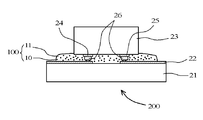
- the light-emitting device 200 includes the connection terminal 22 on the substrate 21 and the connection bumps 26 formed on the n-electrode 24 and the p-electrode 25 of the LED element 23 as light-emitting elements.
- This is a light emitting device in which a light reflective anisotropic conductive adhesive is applied and the substrate 21 and the LED element 23 are flip-chip mounted.
- the cured product 100 of the light-reflective anisotropic conductive adhesive in FIG. 2 includes a cured product 11 of a thermosetting resin composition in which the light-reflective insulating particles (not shown) and the light-reflective conductive particles 10 are formed. It is dispersed inside.
- non-light-reflective conductive particles can be used.
- the light emitting device 200 configured as described above, among the light emitted from the LED elements 23, the light emitted toward the substrate 21 is the light in the cured product 100 of the light-reflective anisotropic conductive adhesive. The light is reflected by the reflective insulating particles and the light-reflective conductive particles 10 and emitted from the upper surface of the LED element 23. Accordingly, it is possible to prevent a decrease in luminous efficiency.
- Configurations other than the light-reflective anisotropic conductive adhesive (the LED element 23, the bump 26, the substrate 21, the connection terminal 22, and the like) in the light-emitting device 200 of the present invention can be the same as the configuration of the conventional light-emitting device. .
- the light emitting device 200 of the present invention can be manufactured by using a conventional anisotropic conductive connection technique except that the light reflective anisotropic conductive adhesive of the present invention is used.
- a well-known light emitting element can be applied in the range which does not impair the effect of this invention other than an LED element.
- Example 1 A colorless transparent thermosetting epoxy binder composition having a refractive index of about 1.50 (YX-8000, JER Co., Ltd .: containing MeHHPA at 50% by mass) and 12 volumes of the following light-reflective insulating particles 1 are contained.
- Au coated resin conductive particles having an average particle size of 5 ⁇ m as conductive particles particles (particles obtained by electroless gold plating of 0.2 ⁇ m thickness on spherical acrylic resin particles having an average particle size of 4.6 ⁇ m (Bright 20GNB4.6EH, Nippon Chemical Industry ( Ltd.) was uniformly mixed at a ratio of 10% by mass to obtain a light-reflective anisotropic conductive adhesive having a white appearance color.
- the obtained light-reflective anisotropic conductive adhesive was applied to a ceramic white plate so as to have a dry thickness of 100 ⁇ m, and heated at 200 ° C. for 1 minute to be cured. About this hardened
- the obtained results are shown in Table 1. It is desired that the total luminous flux is practically 300 mlm or more.
- Example 2 A light-reflective anisotropic conductive adhesive having a white appearance color was obtained in the same manner as in Example 1 except that the blending amount of the light-reflective insulating particles was 7% by volume. Further, similarly to Example 1, a light reflectance evaluation test, a total light flux amount evaluation test and a light resistance test on an LED mounting sample were performed. The obtained results are shown in Table 1.
- Example 3 A light-reflective anisotropic conductive adhesive having a white appearance color was obtained in the same manner as in Example 1 except that the blending amount of the light-reflective insulating particles was 21% by volume. Further, similarly to Example 1, a light reflectance evaluation test, a total light flux amount evaluation test and a light resistance test on an LED mounting sample were performed. The obtained results are shown in Table 1.
- Example 4 instead of Au-coated resin conductive particles, Ni-coated resin conductive particles having an average particle size of 5 ⁇ m (particles obtained by subjecting spherical acrylic resin particles having an average particle size of 4.6 ⁇ m to electroless nickel plating having a thickness of 0.2 ⁇ m) should be used. Except that, a light-reflective anisotropic conductive adhesive having a white appearance color was obtained in the same manner as in Example 1. Further, similarly to Example 1, a light reflectance evaluation test, a total light flux amount evaluation test and a light resistance test on an LED mounting sample were performed. The obtained results are shown in Table 1.
- Examples 5 to 10 and Comparative Example 1 The light-reflective anisotropic conductive adhesives of Examples 5 to 10 having a white appearance color and Comparative Example 1 were obtained in the same manner as Example 1 except that the following light-reflective insulating particles 2 to 8 were used. It was. Further, similarly to Example 1, a light reflectance evaluation test, a total light flux amount evaluation test and a light resistance test on an LED mounting sample were performed. The obtained results are shown in Table 1.
- ⁇ Light reflective insulating particles 1 (used in Examples 1 to 4)> Titanium oxide particles surface-treated with Al 2 O 3 and SiO 2 (KR-380, Titanium Industry Co., Ltd .: particle diameter 0.5 ⁇ m, titanium content 94%)
- ⁇ Light reflective insulating particles 2 (used in Example 5)> Titanium oxide particles surface-treated with Al 2 O 3 and SiO 2 (R-7E, Titanium Industry Co., Ltd .: particle diameter 0.23 ⁇ m, titanium content 85% or slightly over)
- ⁇ Light-reflective insulating particle 3 (used in Example 6)> Titanium oxide particles surface-treated with Al 2 O 3 , SiO 2 and ZrO 2 (D-918, Titanium Industry Co., Ltd .: particle diameter 0.26 ⁇ m, titanium content 88% or slightly over)
- ⁇ Light reflective insulating particles 4 (used in Example 7)> Titanium oxide particles surface-treated with Al 2 O 3 and SiO 2 (R-3L, Titanium Industry Co., Ltd .: particle size 0.23 ⁇ m, titanium content 90% or slightly over)
- ⁇ Light reflecting insulating particles 5 (used in Example 8)> Titanium oxide particles surface-treated with Al 2 O 3 , SiO 2 and ZnO (R-650, Titanium Industry Co., Ltd .: particle diameter 0.23 ⁇ m, titanium content 93% or slightly over)
- ⁇ Light reflective insulating particles 6 (used in Example 9)> Titanium oxide particles surface-treated with Al 2 O 3 (SR-1, Titanium Industry Co., Ltd .: particle diameter 0.25 ⁇ m, titanium content 94% or slightly over)
- ⁇ Light Reflective Insulating Particle 7 (Used in Example 10)> Titanium oxide particles surface-treated with Al 2 O 3 (R-11P, Titanium Industry Co., Ltd .: particle diameter 0.2 ⁇ m, titanium content 95% or slightly over)
- ⁇ Light reflective insulating particles 8 (used in Comparative Example 1)> Titanium oxide particles not surface-treated with metal oxide (R-310, Titanium Industry Co., Ltd .: particle diameter 0.2 ⁇ m, titanium content 97% or slightly over)
- the light reflectivity is 30% or more, and the blue color of light at 450 nm is It was reflected in the same color. Moreover, the total luminous flux was 300 mlm or more. The light resistance was also evaluated at least as “ ⁇ ”.
- the light-reflective anisotropic conductive adhesive of the present invention is used to produce a light-emitting device by flip-chip mounting a light-emitting element such as a light-emitting diode (LED) element on a wiring board using an anisotropic conductive adhesive, Even if a light reflecting layer that causes an increase in manufacturing cost is not provided in the light emitting element, the light emission efficiency can be prevented from being lowered. Moreover, it is excellent also in light resistance. Therefore, the light-reflective anisotropic conductive adhesive of the present invention is useful when flip-chip mounting an LED element.
- a light-emitting element such as a light-emitting diode (LED) element
Landscapes
- Chemical & Material Sciences (AREA)
- Organic Chemistry (AREA)
- Engineering & Computer Science (AREA)
- Microelectronics & Electronic Packaging (AREA)
- Inorganic Chemistry (AREA)
- Physics & Mathematics (AREA)
- Dispersion Chemistry (AREA)
- Spectroscopy & Molecular Physics (AREA)
- Medicinal Chemistry (AREA)
- Polymers & Plastics (AREA)
- Chemical Kinetics & Catalysis (AREA)
- Health & Medical Sciences (AREA)
- Manufacturing & Machinery (AREA)
- Computer Hardware Design (AREA)
- Power Engineering (AREA)
- Led Device Packages (AREA)
- Adhesives Or Adhesive Processes (AREA)
Abstract
Description
屈折率が約1.50の無色透明な熱硬化型エポキシ系バインダー組成物(YX-8000、JER(株):MeHHPAを50質量%で含有)に、以下の光反射性絶縁粒子1を12体積%、導電粒子として平均粒径5μmのAu被覆樹脂導電粒子(平均粒径4.6μmの球状アクリル樹脂粒子に0.2μm厚の無電解金メッキを施した粒子(ブライト20GNB4.6EH、日本化学工業(株))を10質量%となる割合で均一に混合することにより、外観色が白色の光反射性異方性導電接着剤を得た。
得られた光反射性異方性導電接着剤を、セラミック製の白色板に乾燥厚で100μmとなるように塗布し、200℃で1分間加熱し、硬化させた。この硬化物について、分光光度計(U3300、(株)日立製作所)を用いて、波長450nmの光に対する反射率(JIS K7150)を測定した。得られた結果を表1に示す。反射率は、実用上30%以上であることが望まれる。
100μmピッチの銅配線にNi/Au(5.0μm厚/0.3μm厚)メッキ処理した配線を有するガラスエポキシ基板に、バンプボンダー(FB700、(株)カイジョー)を用いて15μm高の金バンプを形成した。この金バンプ付きエポキシ基板に、光反射性異方性導電接着剤を用いて、青色LED(Vf=3.2(If=20mA))を200℃、60秒、1Kg/チップという条件でフリップチップ実装し、テスト用LEDモジュールを得た。
全光束量評価試験に適用したテスト用LEDモジュールを新たに作成し、エージング条件(85℃、85%RH、500時間)下で点灯し続けた。そして、エージング前(初期)後のテスト用LEDモジュールの全光束量を、全光束量評価試験の場合と同様に測定し、以下の評価基準に従って評価した。実用上、少なくとも「△」評価であることが望ましい。
◎:エージング前の全光束量に対するエージング後の全光束量の減少率(%)が5%未満
○:エージング前の全光束量に対するエージング後の全光束量の減少率(%)が5%以上10%未満
△:エージング前の全光束量に対するエージング後の全光束量の減少率(%)が10%以上20%未満
×:エージング前の全光束量に対するエージング後の全光束量の減少率(%)が20%以上
光反射性絶縁粒子の配合量を7体積%とすること以外、実施例1と同様にして外観色が白色の光反射性異方性導電接着剤を得た。また、実施例1と同様に、光反射率評価試験、LED実装サンプルにおける全光束量評価試験及び耐光性試験を行った。得られた結果を表1に示す。
光反射性絶縁粒子の配合量を21体積%とすること以外、実施例1と同様にして外観色が白色の光反射性異方性導電接着剤を得た。また、実施例1と同様に、光反射率評価試験、LED実装サンプルにおける全光束量評価試験及び耐光性試験を行った。得られた結果を表1に示す。
Au被覆樹脂導電粒子に代えて、平均粒径5μmのNi被覆樹脂導電粒子(平均粒径4.6μmの球状アクリル樹脂粒子に0.2μm厚の無電解ニッケルメッキを施した粒子)を使用すること以外、実施例1と同様にして外観色が白色の光反射性異方性導電接着剤を得た。また、実施例1と同様に、光反射率評価試験、LED実装サンプルにおける全光束量評価試験及び耐光性試験を行った。得られた結果を表1に示す。
以下の光反射性絶縁粒子2~8をそれぞれ使用すること以外、実施例1と同様にして外観色が白色の実施例5~10及び比較例1の光反射性異方性導電接着剤を得た。また、実施例1と同様に、光反射率評価試験、LED実装サンプルにおける全光束量評価試験及び耐光性試験を行った。得られた結果を表1に示す。
Al2O3とSiO2とで表面処理された酸化チタン粒子(KR-380、チタン工業(株):粒子径0.5μm、チタン含有量94%)
Al2O3とSiO2とで表面処理された酸化チタン粒子(R-7E、チタン工業(株):粒子径0.23μm、チタン含有量85%又は僅かに超)
Al2O3とSiO2とZrO2とで表面処理された酸化チタン粒子(D-918、チタン工業(株):粒子径0.26μm、チタン含有量88%又は僅かに超)
Al2O3とSiO2とで表面処理された酸化チタン粒子(R-3L、チタン工業(株):粒子径0.23μm、チタン含有量90%又は僅かに超)
Al2O3とSiO2とZnOとで表面処理された酸化チタン粒子(R-650、チタン工業(株):粒子径0.23μm、チタン含有量93%又は僅かに超)
Al2O3で表面処理された酸化チタン粒子(SR-1、チタン工業(株):粒子径0.25μm、チタン含有量94%又は僅かに超)
Al2O3で表面処理された酸化チタン粒子(R-11P、チタン工業(株):粒子径0.2μm、チタン含有量95%又は僅かに超)
金属酸化物で表面処理されていない酸化チタン粒子(R-310、チタン工業(株):粒子径0.2μm、チタン含有量97%又は僅かに超)

2 無機粒子
3 光反射層
4 熱可塑性樹脂
10、20 光反射性導電粒子
11 熱硬化性樹脂組成物の硬化物
21 基板
22 接続端子
23 LED素子
24 n電極
25 p電極
26 バンプ
31 基板
32 ダイボンド接着剤
33 LED素子
34 p電極
35 n電極
36 接続端子
37 金ワイヤ
38 透明モールド樹脂
39 バンプ
40 光反射層
41 異方性導電ペースト
100 光反射性異方性導電接着剤の硬化物
200 発光装置
Claims (20)
- 発光素子を配線板に異方性導電接続するために使用する光反射性異方性導電接着剤であって、熱硬化性樹脂組成物、導電粒子及び光反射性絶縁粒子を含有してなり、該光反射性絶縁粒子が、酸化チタン粒子をそれ以外の金属酸化物で表面処理したものであることを特徴とする光反射性異方性導電接着剤。
- 光反射性絶縁粒子の酸化チタン含有量が、原子数基準で85~93%である請求項1記載の光反射性異方性導電接着剤。
- 該金属酸化物が、Al2O3、SiO、SiO2、ZnO、ZnO2及びZrO2からなる群より選択された少なくとも一種である請求項1又は2記載の光反射性異方性導電接着剤。
- 該金属酸化物が、少なくともAl2O3である請求項3記載の光反射性異方性導電接着剤。
- 該光反射性絶縁粒子の形状が、略球状である請求項1~4のいずれかに記載の光反射性異方性導電接着剤。
- 光反射性絶縁粒子の粒径が、0.2~0.3μmであり、導電粒子の粒径が2~10μmである請求項1~5のいずれかに記載の光反射性異方性導電接着剤。
- 光反射性絶縁粒子の屈折率が、熱硬化性樹脂組成物の硬化物の屈折率よりも大きい請求項1~6のいずれかに記載の光反射性異方性導電接着剤。
- 酸化チタン粒子をそれ以外の金属酸化物で表面処理した光反射性絶縁粒子に加えて、樹脂被覆金属粒子を光反射性絶縁粒子として含有する請求項1~7のいずれかに記載の光反射性異方性導電接着剤。
- 樹脂被覆金属粒子が、鱗片状銀粒子である請求項8記載の光反射性異方性導電接着剤。
- 熱硬化性樹脂組成物に対する光反射性絶縁粒子の配合量が、1~50体積%である請求項1~9のいずれかに記載の光反射性異方性導電接着剤。
- 導電粒子が、金属材料で被覆されているコア粒子と、その表面に酸化亜鉛粒子又は酸化アルミニウム粒子から選択された少なくとも一種の無機粒子から形成された光反射層とからなる光反射性導電粒子である請求項1~10のいずれかに記載の光反射性異方性導電接着剤。
- 導電粒子が、金属材料で被覆されているコア粒子と、その表面に酸化亜鉛粒子から形成された光反射層とからなる光反射性導電粒子である請求項11記載の光反射性異方性導電接着剤。
- コア粒子が樹脂粒子の表面が金属材料で被覆されたものである請求項11又は12記載の光反射性異方性導電接着剤。
- コア粒子の粒径に対する光反射層の層厚が0.5~50%である請求項11~13のいずれかに記載の光反射性異方性導電接着剤。
- 熱硬化性樹脂組成物が、エポキシ系樹脂と酸無水物系硬化剤とを含有する請求項1~14のいずれかに記載の光反射性異方性導電接着剤。
- 熱硬化性樹脂組成物の硬化物の波長380~780nmの可視光に対する光路長1cmの光透過率(JIS K7105)が、80%以上である請求項1~15のいずれかに記載の光反射性異方性導電接着剤。
- 熱硬化性樹脂組成物100質量部に対する光反射性導電粒子の配合量が、1~100質量部である請求項11~16のいずれかに記載の光反射性異方性導電接着剤。
- 光反射性異方性導電接着剤の硬化物の波長450nmに光に対する反射率(JIS K7105)が、少なくとも30%である請求項1~17のいずれかに記載の光反射性異方性導電接着剤。
- 請求項1~18のいずれかに記載の光反射性異方性導電接着剤を介して、発光素子がフリップチップ方式で配線板に実装されている発光装置。
- 発光素子が、発光ダイオードである請求項19記載の発光装置。
Priority Applications (4)
| Application Number | Priority Date | Filing Date | Title |
|---|---|---|---|
| US14/004,553 US9670384B2 (en) | 2011-03-18 | 2012-02-24 | Light-reflective anisotropic conductive adhesive and light-emitting device |
| KR1020137024229A KR20140019349A (ko) | 2011-03-18 | 2012-02-24 | 광반사성 이방성 도전 접착제 및 발광 장치 |
| EP12760304.1A EP2687572B1 (en) | 2011-03-18 | 2012-02-24 | Light-reflective anisotropic conductive adhesive and light-emitting device |
| CN2012800139969A CN103429693A (zh) | 2011-03-18 | 2012-02-24 | 光反射性各向异性导电粘接剂和发光装置 |
Applications Claiming Priority (2)
| Application Number | Priority Date | Filing Date | Title |
|---|---|---|---|
| JP2011060700 | 2011-03-18 | ||
| JP2011-060700 | 2011-03-18 |
Publications (1)
| Publication Number | Publication Date |
|---|---|
| WO2012127978A1 true WO2012127978A1 (ja) | 2012-09-27 |
Family
ID=46879138
Family Applications (1)
| Application Number | Title | Priority Date | Filing Date |
|---|---|---|---|
| PCT/JP2012/054568 WO2012127978A1 (ja) | 2011-03-18 | 2012-02-24 | 光反射性異方性導電接着剤及び発光装置 |
Country Status (7)
| Country | Link |
|---|---|
| US (1) | US9670384B2 (ja) |
| EP (1) | EP2687572B1 (ja) |
| JP (1) | JP2012212865A (ja) |
| KR (1) | KR20140019349A (ja) |
| CN (1) | CN103429693A (ja) |
| TW (1) | TW201241842A (ja) |
| WO (1) | WO2012127978A1 (ja) |
Cited By (3)
| Publication number | Priority date | Publication date | Assignee | Title |
|---|---|---|---|---|
| US20150228414A1 (en) * | 2012-08-22 | 2015-08-13 | Sumitomo Osak Cement Co., Ltd. | Dye-sensitive solar cell paste, porous light-reflective insulation layer, and dye-sensitive solar cell |
| WO2015146275A1 (ja) * | 2014-03-28 | 2015-10-01 | デクセリアルズ株式会社 | 異方性導電フィルム |
| WO2017154978A1 (ja) * | 2016-03-09 | 2017-09-14 | 東洋紡株式会社 | 伸縮性導体シート及び伸縮性導体シート形成用ペースト |
Families Citing this family (8)
| Publication number | Priority date | Publication date | Assignee | Title |
|---|---|---|---|---|
| JP5617210B2 (ja) * | 2009-09-14 | 2014-11-05 | デクセリアルズ株式会社 | 光反射性異方性導電接着剤及び発光装置 |
| JP2013243344A (ja) * | 2012-04-23 | 2013-12-05 | Nichia Chem Ind Ltd | 発光装置 |
| JP6065586B2 (ja) * | 2012-12-28 | 2017-01-25 | 日亜化学工業株式会社 | 発光装置及びその製造方法 |
| TWI556478B (zh) | 2014-06-30 | 2016-11-01 | 億光電子工業股份有限公司 | 發光二極體裝置 |
| JP6844331B2 (ja) * | 2016-03-08 | 2021-03-17 | 東洋紡株式会社 | 伸縮性導体形成用ペースト、伸縮性導体シートおよび生体情報計測用プローブ |
| JP6715052B2 (ja) * | 2016-03-25 | 2020-07-01 | デクセリアルズ株式会社 | 接続構造体の製造方法 |
| JP6935702B2 (ja) * | 2016-10-24 | 2021-09-15 | デクセリアルズ株式会社 | 異方性導電フィルム |
| US11787987B2 (en) | 2018-07-23 | 2023-10-17 | Xerox Corporation | Adhesive with substrate compatibilizing particles |
Citations (5)
| Publication number | Priority date | Publication date | Assignee | Title |
|---|---|---|---|---|
| JPH11168235A (ja) | 1997-12-05 | 1999-06-22 | Toyoda Gosei Co Ltd | 発光ダイオード |
| WO2004044044A1 (ja) * | 2002-11-13 | 2004-05-27 | Idemitsu Kosan Co., Ltd. | 熱可塑性樹脂組成物配合用酸化チタン、熱可塑性樹脂組成物及びその成形体 |
| JP2006145919A (ja) * | 2004-11-19 | 2006-06-08 | Mitsubishi Plastics Ind Ltd | 光反射体及び光反射体の製造方法 |
| JP2010168266A (ja) * | 2008-12-27 | 2010-08-05 | Jgc Catalysts & Chemicals Ltd | 高屈折率金属酸化物微粒子の水分散ゾル、その調製方法および該金属酸化物微粒子の有機溶媒分散ゾル |
| WO2011030621A1 (ja) * | 2009-09-14 | 2011-03-17 | ソニーケミカル&インフォメーションデバイス株式会社 | 光反射性異方性導電接着剤及び発光装置 |
Family Cites Families (9)
| Publication number | Priority date | Publication date | Assignee | Title |
|---|---|---|---|---|
| US4859364A (en) * | 1988-05-25 | 1989-08-22 | E. I. Du Pont De Nemours And Company | Conductive paste composition |
| JP3390278B2 (ja) | 1994-12-05 | 2003-03-24 | ダイセル化学工業株式会社 | セルロースエステル組成物および成形品 |
| JPH09111135A (ja) * | 1995-10-23 | 1997-04-28 | Mitsubishi Materials Corp | 導電性ポリマー組成物 |
| TW201005393A (en) | 2004-11-19 | 2010-02-01 | Mitsubishi Plastics Inc | Light reflecting body and manufacturing method of light reflecting body |
| JP4749201B2 (ja) | 2006-03-31 | 2011-08-17 | 三井化学株式会社 | 半導体発光素子封止用組成物 |
| JP2009139678A (ja) * | 2007-12-07 | 2009-06-25 | Seiko Epson Corp | 発光装置及び電子機器並びに成膜方法 |
| JP5230532B2 (ja) * | 2009-05-29 | 2013-07-10 | 三菱樹脂株式会社 | 白色フィルム、金属積層体、led搭載用基板及び光源装置 |
| JP2011054902A (ja) | 2009-09-04 | 2011-03-17 | Shin-Etsu Chemical Co Ltd | 光半導体ケース形成用白色熱硬化性シリコーン樹脂組成物及び光半導体ケース |
| US8883048B2 (en) | 2009-09-11 | 2014-11-11 | Asahi Kasei Chemicals Corporation | Reflector for light-emitting device, and light-emitting device |
-
2012
- 2012-02-24 CN CN2012800139969A patent/CN103429693A/zh active Pending
- 2012-02-24 KR KR1020137024229A patent/KR20140019349A/ko not_active Application Discontinuation
- 2012-02-24 WO PCT/JP2012/054568 patent/WO2012127978A1/ja active Application Filing
- 2012-02-24 EP EP12760304.1A patent/EP2687572B1/en active Active
- 2012-02-24 US US14/004,553 patent/US9670384B2/en active Active
- 2012-03-01 TW TW101106690A patent/TW201241842A/zh unknown
- 2012-03-01 JP JP2012045401A patent/JP2012212865A/ja active Pending
Patent Citations (5)
| Publication number | Priority date | Publication date | Assignee | Title |
|---|---|---|---|---|
| JPH11168235A (ja) | 1997-12-05 | 1999-06-22 | Toyoda Gosei Co Ltd | 発光ダイオード |
| WO2004044044A1 (ja) * | 2002-11-13 | 2004-05-27 | Idemitsu Kosan Co., Ltd. | 熱可塑性樹脂組成物配合用酸化チタン、熱可塑性樹脂組成物及びその成形体 |
| JP2006145919A (ja) * | 2004-11-19 | 2006-06-08 | Mitsubishi Plastics Ind Ltd | 光反射体及び光反射体の製造方法 |
| JP2010168266A (ja) * | 2008-12-27 | 2010-08-05 | Jgc Catalysts & Chemicals Ltd | 高屈折率金属酸化物微粒子の水分散ゾル、その調製方法および該金属酸化物微粒子の有機溶媒分散ゾル |
| WO2011030621A1 (ja) * | 2009-09-14 | 2011-03-17 | ソニーケミカル&インフォメーションデバイス株式会社 | 光反射性異方性導電接着剤及び発光装置 |
Cited By (7)
| Publication number | Priority date | Publication date | Assignee | Title |
|---|---|---|---|---|
| US20150228414A1 (en) * | 2012-08-22 | 2015-08-13 | Sumitomo Osak Cement Co., Ltd. | Dye-sensitive solar cell paste, porous light-reflective insulation layer, and dye-sensitive solar cell |
| WO2015146275A1 (ja) * | 2014-03-28 | 2015-10-01 | デクセリアルズ株式会社 | 異方性導電フィルム |
| JP2015191823A (ja) * | 2014-03-28 | 2015-11-02 | デクセリアルズ株式会社 | 異方性導電フィルム |
| WO2017154978A1 (ja) * | 2016-03-09 | 2017-09-14 | 東洋紡株式会社 | 伸縮性導体シート及び伸縮性導体シート形成用ペースト |
| JPWO2017154978A1 (ja) * | 2016-03-09 | 2019-01-10 | 東洋紡株式会社 | 伸縮性導体シート及び伸縮性導体シート形成用ペースト |
| TWI708266B (zh) * | 2016-03-09 | 2020-10-21 | 日商東洋紡股份有限公司 | 伸縮性導體片及伸縮性導體片形成用糊劑 |
| TWI736363B (zh) * | 2016-03-09 | 2021-08-11 | 日商東洋紡股份有限公司 | 伸縮性導體片及伸縮性導體片形成用糊劑 |
Also Published As
| Publication number | Publication date |
|---|---|
| US9670384B2 (en) | 2017-06-06 |
| EP2687572B1 (en) | 2018-05-30 |
| EP2687572A4 (en) | 2015-01-07 |
| CN103429693A (zh) | 2013-12-04 |
| TW201241842A (en) | 2012-10-16 |
| JP2012212865A (ja) | 2012-11-01 |
| US20140001419A1 (en) | 2014-01-02 |
| KR20140019349A (ko) | 2014-02-14 |
| TWI563518B (ja) | 2016-12-21 |
| EP2687572A1 (en) | 2014-01-22 |
Similar Documents
| Publication | Publication Date | Title |
|---|---|---|
| WO2012127978A1 (ja) | 光反射性異方性導電接着剤及び発光装置 | |
| JP5617210B2 (ja) | 光反射性異方性導電接着剤及び発光装置 | |
| EP2685513B1 (en) | Light-reflective anisotropic conductive adhesive and light-emitting device | |
| JP5526698B2 (ja) | 光反射性導電粒子、異方性導電接着剤及び発光装置 | |
| JP5888023B2 (ja) | 光反射性異方性導電接着剤及び発光装置 | |
| JP5555038B2 (ja) | 光反射性異方性導電接着剤及び発光装置 | |
| WO2012144033A1 (ja) | 光反射性導電粒子、異方性導電接着剤及び発光装置 | |
| JP5785306B2 (ja) | 光反射性異方性導電接着剤及び発光装置 | |
| JP2014030026A (ja) | 異方性導電接着剤及び発光装置 |
Legal Events
| Date | Code | Title | Description |
|---|---|---|---|
| 121 | Ep: the epo has been informed by wipo that ep was designated in this application |
Ref document number: 12760304 Country of ref document: EP Kind code of ref document: A1 |
|
| DPE2 | Request for preliminary examination filed before expiration of 19th month from priority date (pct application filed from 20040101) | ||
| WWE | Wipo information: entry into national phase |
Ref document number: 14004553 Country of ref document: US |
|
| ENP | Entry into the national phase |
Ref document number: 20137024229 Country of ref document: KR Kind code of ref document: A |
|
| NENP | Non-entry into the national phase |
Ref country code: DE |
|
| WWE | Wipo information: entry into national phase |
Ref document number: 2012760304 Country of ref document: EP |