WO2012144033A1 - 光反射性導電粒子、異方性導電接着剤及び発光装置 - Google Patents
光反射性導電粒子、異方性導電接着剤及び発光装置 Download PDFInfo
- Publication number
- WO2012144033A1 WO2012144033A1 PCT/JP2011/059724 JP2011059724W WO2012144033A1 WO 2012144033 A1 WO2012144033 A1 WO 2012144033A1 JP 2011059724 W JP2011059724 W JP 2011059724W WO 2012144033 A1 WO2012144033 A1 WO 2012144033A1
- Authority
- WO
- WIPO (PCT)
- Prior art keywords
- light
- particles
- anisotropic conductive
- particle
- reflective
- Prior art date
Links
- 239000002245 particle Substances 0.000 title claims abstract description 171
- 239000000853 adhesive Substances 0.000 title claims abstract description 76
- 230000001070 adhesive effect Effects 0.000 title claims abstract description 76
- 239000007771 core particle Substances 0.000 claims abstract description 30
- 239000010954 inorganic particle Substances 0.000 claims abstract description 29
- GWEVSGVZZGPLCZ-UHFFFAOYSA-N Titan oxide Chemical compound O=[Ti]=O GWEVSGVZZGPLCZ-UHFFFAOYSA-N 0.000 claims abstract description 20
- OGIDPMRJRNCKJF-UHFFFAOYSA-N titanium oxide Inorganic materials [Ti]=O OGIDPMRJRNCKJF-UHFFFAOYSA-N 0.000 claims abstract description 19
- 239000007769 metal material Substances 0.000 claims abstract description 18
- XLOMVQKBTHCTTD-UHFFFAOYSA-N Zinc monoxide Chemical compound [Zn]=O XLOMVQKBTHCTTD-UHFFFAOYSA-N 0.000 claims abstract description 12
- TWNQGVIAIRXVLR-UHFFFAOYSA-N oxo(oxoalumanyloxy)alumane Chemical compound O=[Al]O[Al]=O TWNQGVIAIRXVLR-UHFFFAOYSA-N 0.000 claims abstract description 5
- 239000011787 zinc oxide Substances 0.000 claims abstract description 5
- 229920005989 resin Polymers 0.000 claims description 27
- 239000011347 resin Substances 0.000 claims description 27
- 229920001187 thermosetting polymer Polymers 0.000 claims description 25
- PXHVJJICTQNCMI-UHFFFAOYSA-N Nickel Chemical compound [Ni] PXHVJJICTQNCMI-UHFFFAOYSA-N 0.000 claims description 20
- 239000011342 resin composition Substances 0.000 claims description 20
- 239000010931 gold Substances 0.000 claims description 18
- PCHJSUWPFVWCPO-UHFFFAOYSA-N gold Chemical group [Au] PCHJSUWPFVWCPO-UHFFFAOYSA-N 0.000 claims description 15
- 238000000034 method Methods 0.000 claims description 15
- 229910052737 gold Inorganic materials 0.000 claims description 12
- 229920005992 thermoplastic resin Polymers 0.000 claims description 11
- 239000003795 chemical substances by application Substances 0.000 claims description 9
- RYGMFSIKBFXOCR-UHFFFAOYSA-N Copper Chemical compound [Cu] RYGMFSIKBFXOCR-UHFFFAOYSA-N 0.000 claims description 8
- 229910052802 copper Inorganic materials 0.000 claims description 8
- 239000010949 copper Substances 0.000 claims description 8
- 238000002156 mixing Methods 0.000 claims description 8
- 229910052759 nickel Inorganic materials 0.000 claims description 8
- 239000003822 epoxy resin Substances 0.000 claims description 7
- 229920000647 polyepoxide Polymers 0.000 claims description 7
- 150000008065 acid anhydrides Chemical class 0.000 claims description 3
- 230000003287 optical effect Effects 0.000 claims description 3
- 229920000098 polyolefin Polymers 0.000 claims description 3
- 239000010410 layer Substances 0.000 description 36
- 238000012360 testing method Methods 0.000 description 22
- 239000004593 Epoxy Substances 0.000 description 19
- 238000009413 insulation Methods 0.000 description 17
- 239000000843 powder Substances 0.000 description 16
- 150000001875 compounds Chemical class 0.000 description 15
- 238000011156 evaluation Methods 0.000 description 15
- -1 polyethylene Polymers 0.000 description 14
- 239000000126 substance Substances 0.000 description 10
- 230000000052 comparative effect Effects 0.000 description 9
- 239000011230 binding agent Substances 0.000 description 8
- 239000000758 substrate Substances 0.000 description 8
- PPBRXRYQALVLMV-UHFFFAOYSA-N Styrene Chemical compound C=CC1=CC=CC=C1 PPBRXRYQALVLMV-UHFFFAOYSA-N 0.000 description 6
- 230000000694 effects Effects 0.000 description 6
- 239000000463 material Substances 0.000 description 6
- 239000000203 mixture Substances 0.000 description 6
- 238000007747 plating Methods 0.000 description 6
- 229920000178 Acrylic resin Polymers 0.000 description 5
- 239000004925 Acrylic resin Substances 0.000 description 5
- LYCAIKOWRPUZTN-UHFFFAOYSA-N Ethylene glycol Chemical compound OCCO LYCAIKOWRPUZTN-UHFFFAOYSA-N 0.000 description 5
- VYPSYNLAJGMNEJ-UHFFFAOYSA-N Silicium dioxide Chemical compound O=[Si]=O VYPSYNLAJGMNEJ-UHFFFAOYSA-N 0.000 description 5
- 125000002723 alicyclic group Chemical group 0.000 description 5
- RAXXELZNTBOGNW-UHFFFAOYSA-N imidazole Natural products C1=CNC=N1 RAXXELZNTBOGNW-UHFFFAOYSA-N 0.000 description 5
- 239000004698 Polyethylene Substances 0.000 description 4
- 239000004793 Polystyrene Substances 0.000 description 4
- 125000000623 heterocyclic group Chemical group 0.000 description 4
- 238000001579 optical reflectometry Methods 0.000 description 4
- 238000007500 overflow downdraw method Methods 0.000 description 4
- 229920000573 polyethylene Polymers 0.000 description 4
- DNIAPMSPPWPWGF-UHFFFAOYSA-N Propylene glycol Chemical compound CC(O)CO DNIAPMSPPWPWGF-UHFFFAOYSA-N 0.000 description 3
- YXFVVABEGXRONW-UHFFFAOYSA-N Toluene Chemical compound CC1=CC=CC=C1 YXFVVABEGXRONW-UHFFFAOYSA-N 0.000 description 3
- 239000002253 acid Substances 0.000 description 3
- IISBACLAFKSPIT-UHFFFAOYSA-N bisphenol A Chemical compound C=1C=C(O)C=CC=1C(C)(C)C1=CC=C(O)C=C1 IISBACLAFKSPIT-UHFFFAOYSA-N 0.000 description 3
- 230000007423 decrease Effects 0.000 description 3
- 125000003055 glycidyl group Chemical group C(C1CO1)* 0.000 description 3
- 238000004519 manufacturing process Methods 0.000 description 3
- 238000005259 measurement Methods 0.000 description 3
- 238000000691 measurement method Methods 0.000 description 3
- 229910052751 metal Inorganic materials 0.000 description 3
- 239000002184 metal Substances 0.000 description 3
- 229920002223 polystyrene Polymers 0.000 description 3
- 229910052814 silicon oxide Inorganic materials 0.000 description 3
- 238000002834 transmittance Methods 0.000 description 3
- SVTBMSDMJJWYQN-UHFFFAOYSA-N 2-methylpentane-2,4-diol Chemical compound CC(O)CC(C)(C)O SVTBMSDMJJWYQN-UHFFFAOYSA-N 0.000 description 2
- QTWJRLJHJPIABL-UHFFFAOYSA-N 2-methylphenol;3-methylphenol;4-methylphenol Chemical compound CC1=CC=C(O)C=C1.CC1=CC=CC(O)=C1.CC1=CC=CC=C1O QTWJRLJHJPIABL-UHFFFAOYSA-N 0.000 description 2
- PAYRUJLWNCNPSJ-UHFFFAOYSA-N Aniline Chemical compound NC1=CC=CC=C1 PAYRUJLWNCNPSJ-UHFFFAOYSA-N 0.000 description 2
- RTZKZFJDLAIYFH-UHFFFAOYSA-N Diethyl ether Chemical compound CCOCC RTZKZFJDLAIYFH-UHFFFAOYSA-N 0.000 description 2
- BRLQWZUYTZBJKN-UHFFFAOYSA-N Epichlorohydrin Chemical compound ClCC1CO1 BRLQWZUYTZBJKN-UHFFFAOYSA-N 0.000 description 2
- PEDCQBHIVMGVHV-UHFFFAOYSA-N Glycerine Chemical compound OCC(O)CO PEDCQBHIVMGVHV-UHFFFAOYSA-N 0.000 description 2
- QIGBRXMKCJKVMJ-UHFFFAOYSA-N Hydroquinone Chemical compound OC1=CC=C(O)C=C1 QIGBRXMKCJKVMJ-UHFFFAOYSA-N 0.000 description 2
- KDLHZDBZIXYQEI-UHFFFAOYSA-N Palladium Chemical compound [Pd] KDLHZDBZIXYQEI-UHFFFAOYSA-N 0.000 description 2
- KKEYFWRCBNTPAC-UHFFFAOYSA-N Terephthalic acid Chemical compound OC(=O)C1=CC=C(C(O)=O)C=C1 KKEYFWRCBNTPAC-UHFFFAOYSA-N 0.000 description 2
- RTAQQCXQSZGOHL-UHFFFAOYSA-N Titanium Chemical compound [Ti] RTAQQCXQSZGOHL-UHFFFAOYSA-N 0.000 description 2
- 230000032683 aging Effects 0.000 description 2
- PXKLMJQFEQBVLD-UHFFFAOYSA-N bisphenol F Chemical compound C1=CC(O)=CC=C1CC1=CC=C(O)C=C1 PXKLMJQFEQBVLD-UHFFFAOYSA-N 0.000 description 2
- YCIMNLLNPGFGHC-UHFFFAOYSA-N catechol Chemical compound OC1=CC=CC=C1O YCIMNLLNPGFGHC-UHFFFAOYSA-N 0.000 description 2
- 239000011248 coating agent Substances 0.000 description 2
- 238000000576 coating method Methods 0.000 description 2
- 229930003836 cresol Natural products 0.000 description 2
- 230000002950 deficient Effects 0.000 description 2
- 238000000605 extraction Methods 0.000 description 2
- LNEPOXFFQSENCJ-UHFFFAOYSA-N haloperidol Chemical class C1CC(O)(C=2C=CC(Cl)=CC=2)CCN1CCCC(=O)C1=CC=C(F)C=C1 LNEPOXFFQSENCJ-UHFFFAOYSA-N 0.000 description 2
- QQVIHTHCMHWDBS-UHFFFAOYSA-N isophthalic acid Chemical compound OC(=O)C1=CC=CC(C(O)=O)=C1 QQVIHTHCMHWDBS-UHFFFAOYSA-N 0.000 description 2
- VYKXQOYUCMREIS-UHFFFAOYSA-N methylhexahydrophthalic anhydride Chemical compound C1CCCC2C(=O)OC(=O)C21C VYKXQOYUCMREIS-UHFFFAOYSA-N 0.000 description 2
- 229920003986 novolac Polymers 0.000 description 2
- 239000003973 paint Substances 0.000 description 2
- 238000001782 photodegradation Methods 0.000 description 2
- XNGIFLGASWRNHJ-UHFFFAOYSA-N phthalic acid Chemical compound OC(=O)C1=CC=CC=C1C(O)=O XNGIFLGASWRNHJ-UHFFFAOYSA-N 0.000 description 2
- 239000002356 single layer Substances 0.000 description 2
- 239000010936 titanium Substances 0.000 description 2
- 229910052719 titanium Inorganic materials 0.000 description 2
- ARCGXLSVLAOJQL-UHFFFAOYSA-N trimellitic acid Chemical compound OC(=O)C1=CC=C(C(O)=O)C(C(O)=O)=C1 ARCGXLSVLAOJQL-UHFFFAOYSA-N 0.000 description 2
- NIDNOXCRFUCAKQ-UMRXKNAASA-N (1s,2r,3s,4r)-bicyclo[2.2.1]hept-5-ene-2,3-dicarboxylic acid Chemical compound C1[C@H]2C=C[C@@H]1[C@H](C(=O)O)[C@@H]2C(O)=O NIDNOXCRFUCAKQ-UMRXKNAASA-N 0.000 description 1
- JYEUMXHLPRZUAT-UHFFFAOYSA-N 1,2,3-triazine Chemical group C1=CN=NN=C1 JYEUMXHLPRZUAT-UHFFFAOYSA-N 0.000 description 1
- GVPODVKBTHCGFU-UHFFFAOYSA-N 2,4,6-tribromoaniline Chemical compound NC1=C(Br)C=C(Br)C=C1Br GVPODVKBTHCGFU-UHFFFAOYSA-N 0.000 description 1
- LJBWJFWNFUKAGS-UHFFFAOYSA-N 2-[bis(2-hydroxyphenyl)methyl]phenol Chemical compound OC1=CC=CC=C1C(C=1C(=CC=CC=1)O)C1=CC=CC=C1O LJBWJFWNFUKAGS-UHFFFAOYSA-N 0.000 description 1
- CDAWCLOXVUBKRW-UHFFFAOYSA-N 2-aminophenol Chemical compound NC1=CC=CC=C1O CDAWCLOXVUBKRW-UHFFFAOYSA-N 0.000 description 1
- VEORPZCZECFIRK-UHFFFAOYSA-N 3,3',5,5'-tetrabromobisphenol A Chemical compound C=1C(Br)=C(O)C(Br)=CC=1C(C)(C)C1=CC(Br)=C(O)C(Br)=C1 VEORPZCZECFIRK-UHFFFAOYSA-N 0.000 description 1
- ALKYHXVLJMQRLQ-UHFFFAOYSA-N 3-Hydroxy-2-naphthoate Chemical compound C1=CC=C2C=C(O)C(C(=O)O)=CC2=C1 ALKYHXVLJMQRLQ-UHFFFAOYSA-N 0.000 description 1
- IBFJDBNISOJRCW-UHFFFAOYSA-N 3-methylphthalic acid Chemical compound CC1=CC=CC(C(O)=O)=C1C(O)=O IBFJDBNISOJRCW-UHFFFAOYSA-N 0.000 description 1
- YBRVSVVVWCFQMG-UHFFFAOYSA-N 4,4'-diaminodiphenylmethane Chemical compound C1=CC(N)=CC=C1CC1=CC=C(N)C=C1 YBRVSVVVWCFQMG-UHFFFAOYSA-N 0.000 description 1
- VPWNQTHUCYMVMZ-UHFFFAOYSA-N 4,4'-sulfonyldiphenol Chemical compound C1=CC(O)=CC=C1S(=O)(=O)C1=CC=C(O)C=C1 VPWNQTHUCYMVMZ-UHFFFAOYSA-N 0.000 description 1
- ODJUOZPKKHIEOZ-UHFFFAOYSA-N 4-[2-(4-hydroxy-3,5-dimethylphenyl)propan-2-yl]-2,6-dimethylphenol Chemical compound CC1=C(O)C(C)=CC(C(C)(C)C=2C=C(C)C(O)=C(C)C=2)=C1 ODJUOZPKKHIEOZ-UHFFFAOYSA-N 0.000 description 1
- ALYNCZNDIQEVRV-UHFFFAOYSA-N 4-aminobenzoic acid Chemical compound NC1=CC=C(C(O)=O)C=C1 ALYNCZNDIQEVRV-UHFFFAOYSA-N 0.000 description 1
- XRBNDLYHPCVYGC-UHFFFAOYSA-N 4-phenylbenzene-1,2,3-triol Chemical group OC1=C(O)C(O)=CC=C1C1=CC=CC=C1 XRBNDLYHPCVYGC-UHFFFAOYSA-N 0.000 description 1
- GZVHEAJQGPRDLQ-UHFFFAOYSA-N 6-phenyl-1,3,5-triazine-2,4-diamine Chemical compound NC1=NC(N)=NC(C=2C=CC=CC=2)=N1 GZVHEAJQGPRDLQ-UHFFFAOYSA-N 0.000 description 1
- 229910018072 Al 2 O 3 Inorganic materials 0.000 description 1
- 229930185605 Bisphenol Natural products 0.000 description 1
- 229920002799 BoPET Polymers 0.000 description 1
- MQJKPEGWNLWLTK-UHFFFAOYSA-N Dapsone Chemical compound C1=CC(N)=CC=C1S(=O)(=O)C1=CC=C(N)C=C1 MQJKPEGWNLWLTK-UHFFFAOYSA-N 0.000 description 1
- 239000004677 Nylon Substances 0.000 description 1
- ISWSIDIOOBJBQZ-UHFFFAOYSA-N Phenol Chemical compound OC1=CC=CC=C1 ISWSIDIOOBJBQZ-UHFFFAOYSA-N 0.000 description 1
- 239000004743 Polypropylene Substances 0.000 description 1
- 239000004820 Pressure-sensitive adhesive Substances 0.000 description 1
- BQCADISMDOOEFD-UHFFFAOYSA-N Silver Chemical compound [Ag] BQCADISMDOOEFD-UHFFFAOYSA-N 0.000 description 1
- 239000007983 Tris buffer Substances 0.000 description 1
- GKXVJHDEWHKBFH-UHFFFAOYSA-N [2-(aminomethyl)phenyl]methanamine Chemical compound NCC1=CC=CC=C1CN GKXVJHDEWHKBFH-UHFFFAOYSA-N 0.000 description 1
- 239000012790 adhesive layer Substances 0.000 description 1
- 125000001931 aliphatic group Chemical group 0.000 description 1
- 229910045601 alloy Inorganic materials 0.000 description 1
- 239000000956 alloy Substances 0.000 description 1
- 229910052782 aluminium Inorganic materials 0.000 description 1
- XAGFODPZIPBFFR-UHFFFAOYSA-N aluminium Chemical compound [Al] XAGFODPZIPBFFR-UHFFFAOYSA-N 0.000 description 1
- 229960004050 aminobenzoic acid Drugs 0.000 description 1
- RWCCWEUUXYIKHB-UHFFFAOYSA-N benzophenone Chemical compound C=1C=CC=CC=1C(=O)C1=CC=CC=C1 RWCCWEUUXYIKHB-UHFFFAOYSA-N 0.000 description 1
- 239000012965 benzophenone Substances 0.000 description 1
- 230000005540 biological transmission Effects 0.000 description 1
- BVKZGUZCCUSVTD-UHFFFAOYSA-N carbonic acid Chemical compound OC(O)=O BVKZGUZCCUSVTD-UHFFFAOYSA-N 0.000 description 1
- 230000003197 catalytic effect Effects 0.000 description 1
- 239000000919 ceramic Substances 0.000 description 1
- 238000004040 coloring Methods 0.000 description 1
- 238000013329 compounding Methods 0.000 description 1
- 239000004020 conductor Substances 0.000 description 1
- 239000000470 constituent Substances 0.000 description 1
- 238000001816 cooling Methods 0.000 description 1
- 238000005260 corrosion Methods 0.000 description 1
- 230000007797 corrosion Effects 0.000 description 1
- 230000001351 cycling effect Effects 0.000 description 1
- IFDVQVHZEKPUSC-UHFFFAOYSA-N cyclohex-3-ene-1,2-dicarboxylic acid Chemical compound OC(=O)C1CCC=CC1C(O)=O IFDVQVHZEKPUSC-UHFFFAOYSA-N 0.000 description 1
- YMHQVDAATAEZLO-UHFFFAOYSA-N cyclohexane-1,1-diamine Chemical compound NC1(N)CCCCC1 YMHQVDAATAEZLO-UHFFFAOYSA-N 0.000 description 1
- 230000003247 decreasing effect Effects 0.000 description 1
- 235000014113 dietary fatty acids Nutrition 0.000 description 1
- 238000009792 diffusion process Methods 0.000 description 1
- GYZLOYUZLJXAJU-UHFFFAOYSA-N diglycidyl ether Chemical compound C1OC1COCC1CO1 GYZLOYUZLJXAJU-UHFFFAOYSA-N 0.000 description 1
- 238000007772 electroless plating Methods 0.000 description 1
- 238000009713 electroplating Methods 0.000 description 1
- 230000007613 environmental effect Effects 0.000 description 1
- 125000003700 epoxy group Chemical group 0.000 description 1
- 150000002148 esters Chemical class 0.000 description 1
- 239000000194 fatty acid Substances 0.000 description 1
- 229930195729 fatty acid Natural products 0.000 description 1
- 150000004665 fatty acids Chemical class 0.000 description 1
- 239000010419 fine particle Substances 0.000 description 1
- 239000011521 glass Substances 0.000 description 1
- 235000011187 glycerol Nutrition 0.000 description 1
- 238000010438 heat treatment Methods 0.000 description 1
- VBZWSGALLODQNC-UHFFFAOYSA-N hexafluoroacetone Chemical compound FC(F)(F)C(=O)C(F)(F)F VBZWSGALLODQNC-UHFFFAOYSA-N 0.000 description 1
- 229940051250 hexylene glycol Drugs 0.000 description 1
- WGCNASOHLSPBMP-UHFFFAOYSA-N hydroxyacetaldehyde Natural products OCC=O WGCNASOHLSPBMP-UHFFFAOYSA-N 0.000 description 1
- 230000001771 impaired effect Effects 0.000 description 1
- 239000007788 liquid Substances 0.000 description 1
- ZLNQQNXFFQJAID-UHFFFAOYSA-L magnesium carbonate Chemical compound [Mg+2].[O-]C([O-])=O ZLNQQNXFFQJAID-UHFFFAOYSA-L 0.000 description 1
- 239000001095 magnesium carbonate Substances 0.000 description 1
- 229910000021 magnesium carbonate Inorganic materials 0.000 description 1
- SLCVBVWXLSEKPL-UHFFFAOYSA-N neopentyl glycol Chemical compound OCC(C)(C)CO SLCVBVWXLSEKPL-UHFFFAOYSA-N 0.000 description 1
- 229920001778 nylon Polymers 0.000 description 1
- JMANVNJQNLATNU-UHFFFAOYSA-N oxalonitrile Chemical compound N#CC#N JMANVNJQNLATNU-UHFFFAOYSA-N 0.000 description 1
- ZXQPRTUUOOOZAS-UHFFFAOYSA-N oxiran-2-yl(oxiran-2-ylmethoxy)methanamine Chemical compound C1OC1C(N)OCC1CO1 ZXQPRTUUOOOZAS-UHFFFAOYSA-N 0.000 description 1
- AFEQENGXSMURHA-UHFFFAOYSA-N oxiran-2-ylmethanamine Chemical compound NCC1CO1 AFEQENGXSMURHA-UHFFFAOYSA-N 0.000 description 1
- 229910052763 palladium Inorganic materials 0.000 description 1
- 229920001155 polypropylene Polymers 0.000 description 1
- 229920001451 polypropylene glycol Polymers 0.000 description 1
- GHMLBKRAJCXXBS-UHFFFAOYSA-N resorcinol Chemical compound OC1=CC=CC(O)=C1 GHMLBKRAJCXXBS-UHFFFAOYSA-N 0.000 description 1
- 229960001755 resorcinol Drugs 0.000 description 1
- 239000000377 silicon dioxide Substances 0.000 description 1
- 229910052709 silver Inorganic materials 0.000 description 1
- 239000004332 silver Substances 0.000 description 1
- 229910000679 solder Inorganic materials 0.000 description 1
- 239000007787 solid Substances 0.000 description 1
- 239000002904 solvent Substances 0.000 description 1
- 150000005846 sugar alcohols Polymers 0.000 description 1
- UFDHBDMSHIXOKF-UHFFFAOYSA-N tetrahydrophthalic acid Natural products OC(=O)C1=C(C(O)=O)CCCC1 UFDHBDMSHIXOKF-UHFFFAOYSA-N 0.000 description 1
- 150000004992 toluidines Chemical class 0.000 description 1
- 238000007740 vapor deposition Methods 0.000 description 1
Images


Classifications
-
- H—ELECTRICITY
- H01—ELECTRIC ELEMENTS
- H01B—CABLES; CONDUCTORS; INSULATORS; SELECTION OF MATERIALS FOR THEIR CONDUCTIVE, INSULATING OR DIELECTRIC PROPERTIES
- H01B1/00—Conductors or conductive bodies characterised by the conductive materials; Selection of materials as conductors
- H01B1/02—Conductors or conductive bodies characterised by the conductive materials; Selection of materials as conductors mainly consisting of metals or alloys
-
- C—CHEMISTRY; METALLURGY
- C08—ORGANIC MACROMOLECULAR COMPOUNDS; THEIR PREPARATION OR CHEMICAL WORKING-UP; COMPOSITIONS BASED THEREON
- C08G—MACROMOLECULAR COMPOUNDS OBTAINED OTHERWISE THAN BY REACTIONS ONLY INVOLVING UNSATURATED CARBON-TO-CARBON BONDS
- C08G59/00—Polycondensates containing more than one epoxy group per molecule; Macromolecules obtained by polymerising compounds containing more than one epoxy group per molecule using curing agents or catalysts which react with the epoxy groups
- C08G59/18—Macromolecules obtained by polymerising compounds containing more than one epoxy group per molecule using curing agents or catalysts which react with the epoxy groups ; e.g. general methods of curing
- C08G59/40—Macromolecules obtained by polymerising compounds containing more than one epoxy group per molecule using curing agents or catalysts which react with the epoxy groups ; e.g. general methods of curing characterised by the curing agents used
- C08G59/42—Polycarboxylic acids; Anhydrides, halides or low molecular weight esters thereof
-
- C—CHEMISTRY; METALLURGY
- C09—DYES; PAINTS; POLISHES; NATURAL RESINS; ADHESIVES; COMPOSITIONS NOT OTHERWISE PROVIDED FOR; APPLICATIONS OF MATERIALS NOT OTHERWISE PROVIDED FOR
- C09J—ADHESIVES; NON-MECHANICAL ASPECTS OF ADHESIVE PROCESSES IN GENERAL; ADHESIVE PROCESSES NOT PROVIDED FOR ELSEWHERE; USE OF MATERIALS AS ADHESIVES
- C09J11/00—Features of adhesives not provided for in group C09J9/00, e.g. additives
- C09J11/02—Non-macromolecular additives
- C09J11/04—Non-macromolecular additives inorganic
-
- C—CHEMISTRY; METALLURGY
- C09—DYES; PAINTS; POLISHES; NATURAL RESINS; ADHESIVES; COMPOSITIONS NOT OTHERWISE PROVIDED FOR; APPLICATIONS OF MATERIALS NOT OTHERWISE PROVIDED FOR
- C09J—ADHESIVES; NON-MECHANICAL ASPECTS OF ADHESIVE PROCESSES IN GENERAL; ADHESIVE PROCESSES NOT PROVIDED FOR ELSEWHERE; USE OF MATERIALS AS ADHESIVES
- C09J163/00—Adhesives based on epoxy resins; Adhesives based on derivatives of epoxy resins
-
- C—CHEMISTRY; METALLURGY
- C09—DYES; PAINTS; POLISHES; NATURAL RESINS; ADHESIVES; COMPOSITIONS NOT OTHERWISE PROVIDED FOR; APPLICATIONS OF MATERIALS NOT OTHERWISE PROVIDED FOR
- C09J—ADHESIVES; NON-MECHANICAL ASPECTS OF ADHESIVE PROCESSES IN GENERAL; ADHESIVE PROCESSES NOT PROVIDED FOR ELSEWHERE; USE OF MATERIALS AS ADHESIVES
- C09J9/00—Adhesives characterised by their physical nature or the effects produced, e.g. glue sticks
- C09J9/02—Electrically-conducting adhesives
-
- H—ELECTRICITY
- H01—ELECTRIC ELEMENTS
- H01B—CABLES; CONDUCTORS; INSULATORS; SELECTION OF MATERIALS FOR THEIR CONDUCTIVE, INSULATING OR DIELECTRIC PROPERTIES
- H01B1/00—Conductors or conductive bodies characterised by the conductive materials; Selection of materials as conductors
- H01B1/20—Conductive material dispersed in non-conductive organic material
- H01B1/22—Conductive material dispersed in non-conductive organic material the conductive material comprising metals or alloys
-
- H—ELECTRICITY
- H01—ELECTRIC ELEMENTS
- H01L—SEMICONDUCTOR DEVICES NOT COVERED BY CLASS H10
- H01L24/00—Arrangements for connecting or disconnecting semiconductor or solid-state bodies; Methods or apparatus related thereto
- H01L24/01—Means for bonding being attached to, or being formed on, the surface to be connected, e.g. chip-to-package, die-attach, "first-level" interconnects; Manufacturing methods related thereto
- H01L24/26—Layer connectors, e.g. plate connectors, solder or adhesive layers; Manufacturing methods related thereto
- H01L24/28—Structure, shape, material or disposition of the layer connectors prior to the connecting process
- H01L24/29—Structure, shape, material or disposition of the layer connectors prior to the connecting process of an individual layer connector
-
- H—ELECTRICITY
- H01—ELECTRIC ELEMENTS
- H01L—SEMICONDUCTOR DEVICES NOT COVERED BY CLASS H10
- H01L33/00—Semiconductor devices having potential barriers specially adapted for light emission; Processes or apparatus specially adapted for the manufacture or treatment thereof or of parts thereof; Details thereof
- H01L33/48—Semiconductor devices having potential barriers specially adapted for light emission; Processes or apparatus specially adapted for the manufacture or treatment thereof or of parts thereof; Details thereof characterised by the semiconductor body packages
- H01L33/58—Optical field-shaping elements
- H01L33/60—Reflective elements
-
- H—ELECTRICITY
- H01—ELECTRIC ELEMENTS
- H01L—SEMICONDUCTOR DEVICES NOT COVERED BY CLASS H10
- H01L33/00—Semiconductor devices having potential barriers specially adapted for light emission; Processes or apparatus specially adapted for the manufacture or treatment thereof or of parts thereof; Details thereof
- H01L33/48—Semiconductor devices having potential barriers specially adapted for light emission; Processes or apparatus specially adapted for the manufacture or treatment thereof or of parts thereof; Details thereof characterised by the semiconductor body packages
- H01L33/62—Arrangements for conducting electric current to or from the semiconductor body, e.g. lead-frames, wire-bonds or solder balls
-
- C—CHEMISTRY; METALLURGY
- C08—ORGANIC MACROMOLECULAR COMPOUNDS; THEIR PREPARATION OR CHEMICAL WORKING-UP; COMPOSITIONS BASED THEREON
- C08K—Use of inorganic or non-macromolecular organic substances as compounding ingredients
- C08K9/00—Use of pretreated ingredients
- C08K9/02—Ingredients treated with inorganic substances
-
- H—ELECTRICITY
- H01—ELECTRIC ELEMENTS
- H01L—SEMICONDUCTOR DEVICES NOT COVERED BY CLASS H10
- H01L2224/00—Indexing scheme for arrangements for connecting or disconnecting semiconductor or solid-state bodies and methods related thereto as covered by H01L24/00
- H01L2224/01—Means for bonding being attached to, or being formed on, the surface to be connected, e.g. chip-to-package, die-attach, "first-level" interconnects; Manufacturing methods related thereto
- H01L2224/02—Bonding areas; Manufacturing methods related thereto
- H01L2224/04—Structure, shape, material or disposition of the bonding areas prior to the connecting process
- H01L2224/05—Structure, shape, material or disposition of the bonding areas prior to the connecting process of an individual bonding area
- H01L2224/0554—External layer
- H01L2224/0556—Disposition
- H01L2224/05568—Disposition the whole external layer protruding from the surface
-
- H—ELECTRICITY
- H01—ELECTRIC ELEMENTS
- H01L—SEMICONDUCTOR DEVICES NOT COVERED BY CLASS H10
- H01L2224/00—Indexing scheme for arrangements for connecting or disconnecting semiconductor or solid-state bodies and methods related thereto as covered by H01L24/00
- H01L2224/01—Means for bonding being attached to, or being formed on, the surface to be connected, e.g. chip-to-package, die-attach, "first-level" interconnects; Manufacturing methods related thereto
- H01L2224/02—Bonding areas; Manufacturing methods related thereto
- H01L2224/04—Structure, shape, material or disposition of the bonding areas prior to the connecting process
- H01L2224/05—Structure, shape, material or disposition of the bonding areas prior to the connecting process of an individual bonding area
- H01L2224/0554—External layer
- H01L2224/05573—Single external layer
-
- H—ELECTRICITY
- H01—ELECTRIC ELEMENTS
- H01L—SEMICONDUCTOR DEVICES NOT COVERED BY CLASS H10
- H01L2224/00—Indexing scheme for arrangements for connecting or disconnecting semiconductor or solid-state bodies and methods related thereto as covered by H01L24/00
- H01L2224/01—Means for bonding being attached to, or being formed on, the surface to be connected, e.g. chip-to-package, die-attach, "first-level" interconnects; Manufacturing methods related thereto
- H01L2224/10—Bump connectors; Manufacturing methods related thereto
- H01L2224/15—Structure, shape, material or disposition of the bump connectors after the connecting process
- H01L2224/16—Structure, shape, material or disposition of the bump connectors after the connecting process of an individual bump connector
- H01L2224/161—Disposition
- H01L2224/16151—Disposition the bump connector connecting between a semiconductor or solid-state body and an item not being a semiconductor or solid-state body, e.g. chip-to-substrate, chip-to-passive
- H01L2224/16221—Disposition the bump connector connecting between a semiconductor or solid-state body and an item not being a semiconductor or solid-state body, e.g. chip-to-substrate, chip-to-passive the body and the item being stacked
- H01L2224/16225—Disposition the bump connector connecting between a semiconductor or solid-state body and an item not being a semiconductor or solid-state body, e.g. chip-to-substrate, chip-to-passive the body and the item being stacked the item being non-metallic, e.g. insulating substrate with or without metallisation
- H01L2224/16227—Disposition the bump connector connecting between a semiconductor or solid-state body and an item not being a semiconductor or solid-state body, e.g. chip-to-substrate, chip-to-passive the body and the item being stacked the item being non-metallic, e.g. insulating substrate with or without metallisation the bump connector connecting to a bond pad of the item
-
- H—ELECTRICITY
- H01—ELECTRIC ELEMENTS
- H01L—SEMICONDUCTOR DEVICES NOT COVERED BY CLASS H10
- H01L2224/00—Indexing scheme for arrangements for connecting or disconnecting semiconductor or solid-state bodies and methods related thereto as covered by H01L24/00
- H01L2224/01—Means for bonding being attached to, or being formed on, the surface to be connected, e.g. chip-to-package, die-attach, "first-level" interconnects; Manufacturing methods related thereto
- H01L2224/26—Layer connectors, e.g. plate connectors, solder or adhesive layers; Manufacturing methods related thereto
- H01L2224/28—Structure, shape, material or disposition of the layer connectors prior to the connecting process
- H01L2224/29—Structure, shape, material or disposition of the layer connectors prior to the connecting process of an individual layer connector
- H01L2224/29001—Core members of the layer connector
- H01L2224/29099—Material
- H01L2224/29198—Material with a principal constituent of the material being a combination of two or more materials in the form of a matrix with a filler, i.e. being a hybrid material, e.g. segmented structures, foams
- H01L2224/29199—Material of the matrix
- H01L2224/2929—Material of the matrix with a principal constituent of the material being a polymer, e.g. polyester, phenolic based polymer, epoxy
-
- H—ELECTRICITY
- H01—ELECTRIC ELEMENTS
- H01L—SEMICONDUCTOR DEVICES NOT COVERED BY CLASS H10
- H01L2224/00—Indexing scheme for arrangements for connecting or disconnecting semiconductor or solid-state bodies and methods related thereto as covered by H01L24/00
- H01L2224/01—Means for bonding being attached to, or being formed on, the surface to be connected, e.g. chip-to-package, die-attach, "first-level" interconnects; Manufacturing methods related thereto
- H01L2224/26—Layer connectors, e.g. plate connectors, solder or adhesive layers; Manufacturing methods related thereto
- H01L2224/28—Structure, shape, material or disposition of the layer connectors prior to the connecting process
- H01L2224/29—Structure, shape, material or disposition of the layer connectors prior to the connecting process of an individual layer connector
- H01L2224/29001—Core members of the layer connector
- H01L2224/29099—Material
- H01L2224/29198—Material with a principal constituent of the material being a combination of two or more materials in the form of a matrix with a filler, i.e. being a hybrid material, e.g. segmented structures, foams
- H01L2224/29298—Fillers
- H01L2224/29299—Base material
- H01L2224/2939—Base material with a principal constituent of the material being a polymer, e.g. polyester, phenolic based polymer, epoxy
-
- H—ELECTRICITY
- H01—ELECTRIC ELEMENTS
- H01L—SEMICONDUCTOR DEVICES NOT COVERED BY CLASS H10
- H01L2224/00—Indexing scheme for arrangements for connecting or disconnecting semiconductor or solid-state bodies and methods related thereto as covered by H01L24/00
- H01L2224/01—Means for bonding being attached to, or being formed on, the surface to be connected, e.g. chip-to-package, die-attach, "first-level" interconnects; Manufacturing methods related thereto
- H01L2224/26—Layer connectors, e.g. plate connectors, solder or adhesive layers; Manufacturing methods related thereto
- H01L2224/28—Structure, shape, material or disposition of the layer connectors prior to the connecting process
- H01L2224/29—Structure, shape, material or disposition of the layer connectors prior to the connecting process of an individual layer connector
- H01L2224/29001—Core members of the layer connector
- H01L2224/29099—Material
- H01L2224/29198—Material with a principal constituent of the material being a combination of two or more materials in the form of a matrix with a filler, i.e. being a hybrid material, e.g. segmented structures, foams
- H01L2224/29298—Fillers
- H01L2224/29299—Base material
- H01L2224/29393—Base material with a principal constituent of the material being a solid not provided for in groups H01L2224/293 - H01L2224/29391, e.g. allotropes of carbon, fullerene, graphite, carbon-nanotubes, diamond
-
- H—ELECTRICITY
- H01—ELECTRIC ELEMENTS
- H01L—SEMICONDUCTOR DEVICES NOT COVERED BY CLASS H10
- H01L2224/00—Indexing scheme for arrangements for connecting or disconnecting semiconductor or solid-state bodies and methods related thereto as covered by H01L24/00
- H01L2224/01—Means for bonding being attached to, or being formed on, the surface to be connected, e.g. chip-to-package, die-attach, "first-level" interconnects; Manufacturing methods related thereto
- H01L2224/26—Layer connectors, e.g. plate connectors, solder or adhesive layers; Manufacturing methods related thereto
- H01L2224/28—Structure, shape, material or disposition of the layer connectors prior to the connecting process
- H01L2224/29—Structure, shape, material or disposition of the layer connectors prior to the connecting process of an individual layer connector
- H01L2224/29001—Core members of the layer connector
- H01L2224/29099—Material
- H01L2224/29198—Material with a principal constituent of the material being a combination of two or more materials in the form of a matrix with a filler, i.e. being a hybrid material, e.g. segmented structures, foams
- H01L2224/29298—Fillers
- H01L2224/29399—Coating material
- H01L2224/294—Coating material with a principal constituent of the material being a metal or a metalloid, e.g. boron [B], silicon [Si], germanium [Ge], arsenic [As], antimony [Sb], tellurium [Te] and polonium [Po], and alloys thereof
- H01L2224/29438—Coating material with a principal constituent of the material being a metal or a metalloid, e.g. boron [B], silicon [Si], germanium [Ge], arsenic [As], antimony [Sb], tellurium [Te] and polonium [Po], and alloys thereof the principal constituent melting at a temperature of greater than or equal to 950°C and less than 1550°C
- H01L2224/29444—Gold [Au] as principal constituent
-
- H—ELECTRICITY
- H01—ELECTRIC ELEMENTS
- H01L—SEMICONDUCTOR DEVICES NOT COVERED BY CLASS H10
- H01L2224/00—Indexing scheme for arrangements for connecting or disconnecting semiconductor or solid-state bodies and methods related thereto as covered by H01L24/00
- H01L2224/01—Means for bonding being attached to, or being formed on, the surface to be connected, e.g. chip-to-package, die-attach, "first-level" interconnects; Manufacturing methods related thereto
- H01L2224/26—Layer connectors, e.g. plate connectors, solder or adhesive layers; Manufacturing methods related thereto
- H01L2224/28—Structure, shape, material or disposition of the layer connectors prior to the connecting process
- H01L2224/29—Structure, shape, material or disposition of the layer connectors prior to the connecting process of an individual layer connector
- H01L2224/29001—Core members of the layer connector
- H01L2224/29099—Material
- H01L2224/29198—Material with a principal constituent of the material being a combination of two or more materials in the form of a matrix with a filler, i.e. being a hybrid material, e.g. segmented structures, foams
- H01L2224/29298—Fillers
- H01L2224/29399—Coating material
- H01L2224/294—Coating material with a principal constituent of the material being a metal or a metalloid, e.g. boron [B], silicon [Si], germanium [Ge], arsenic [As], antimony [Sb], tellurium [Te] and polonium [Po], and alloys thereof
- H01L2224/29438—Coating material with a principal constituent of the material being a metal or a metalloid, e.g. boron [B], silicon [Si], germanium [Ge], arsenic [As], antimony [Sb], tellurium [Te] and polonium [Po], and alloys thereof the principal constituent melting at a temperature of greater than or equal to 950°C and less than 1550°C
- H01L2224/29447—Copper [Cu] as principal constituent
-
- H—ELECTRICITY
- H01—ELECTRIC ELEMENTS
- H01L—SEMICONDUCTOR DEVICES NOT COVERED BY CLASS H10
- H01L2224/00—Indexing scheme for arrangements for connecting or disconnecting semiconductor or solid-state bodies and methods related thereto as covered by H01L24/00
- H01L2224/01—Means for bonding being attached to, or being formed on, the surface to be connected, e.g. chip-to-package, die-attach, "first-level" interconnects; Manufacturing methods related thereto
- H01L2224/26—Layer connectors, e.g. plate connectors, solder or adhesive layers; Manufacturing methods related thereto
- H01L2224/28—Structure, shape, material or disposition of the layer connectors prior to the connecting process
- H01L2224/29—Structure, shape, material or disposition of the layer connectors prior to the connecting process of an individual layer connector
- H01L2224/29001—Core members of the layer connector
- H01L2224/29099—Material
- H01L2224/29198—Material with a principal constituent of the material being a combination of two or more materials in the form of a matrix with a filler, i.e. being a hybrid material, e.g. segmented structures, foams
- H01L2224/29298—Fillers
- H01L2224/29399—Coating material
- H01L2224/294—Coating material with a principal constituent of the material being a metal or a metalloid, e.g. boron [B], silicon [Si], germanium [Ge], arsenic [As], antimony [Sb], tellurium [Te] and polonium [Po], and alloys thereof
- H01L2224/29438—Coating material with a principal constituent of the material being a metal or a metalloid, e.g. boron [B], silicon [Si], germanium [Ge], arsenic [As], antimony [Sb], tellurium [Te] and polonium [Po], and alloys thereof the principal constituent melting at a temperature of greater than or equal to 950°C and less than 1550°C
- H01L2224/29455—Nickel [Ni] as principal constituent
-
- H—ELECTRICITY
- H01—ELECTRIC ELEMENTS
- H01L—SEMICONDUCTOR DEVICES NOT COVERED BY CLASS H10
- H01L2224/00—Indexing scheme for arrangements for connecting or disconnecting semiconductor or solid-state bodies and methods related thereto as covered by H01L24/00
- H01L2224/01—Means for bonding being attached to, or being formed on, the surface to be connected, e.g. chip-to-package, die-attach, "first-level" interconnects; Manufacturing methods related thereto
- H01L2224/26—Layer connectors, e.g. plate connectors, solder or adhesive layers; Manufacturing methods related thereto
- H01L2224/31—Structure, shape, material or disposition of the layer connectors after the connecting process
- H01L2224/32—Structure, shape, material or disposition of the layer connectors after the connecting process of an individual layer connector
- H01L2224/321—Disposition
- H01L2224/32151—Disposition the layer connector connecting between a semiconductor or solid-state body and an item not being a semiconductor or solid-state body, e.g. chip-to-substrate, chip-to-passive
- H01L2224/32221—Disposition the layer connector connecting between a semiconductor or solid-state body and an item not being a semiconductor or solid-state body, e.g. chip-to-substrate, chip-to-passive the body and the item being stacked
- H01L2224/32225—Disposition the layer connector connecting between a semiconductor or solid-state body and an item not being a semiconductor or solid-state body, e.g. chip-to-substrate, chip-to-passive the body and the item being stacked the item being non-metallic, e.g. insulating substrate with or without metallisation
-
- H—ELECTRICITY
- H01—ELECTRIC ELEMENTS
- H01L—SEMICONDUCTOR DEVICES NOT COVERED BY CLASS H10
- H01L2224/00—Indexing scheme for arrangements for connecting or disconnecting semiconductor or solid-state bodies and methods related thereto as covered by H01L24/00
- H01L2224/01—Means for bonding being attached to, or being formed on, the surface to be connected, e.g. chip-to-package, die-attach, "first-level" interconnects; Manufacturing methods related thereto
- H01L2224/42—Wire connectors; Manufacturing methods related thereto
- H01L2224/44—Structure, shape, material or disposition of the wire connectors prior to the connecting process
- H01L2224/45—Structure, shape, material or disposition of the wire connectors prior to the connecting process of an individual wire connector
- H01L2224/45001—Core members of the connector
- H01L2224/45099—Material
- H01L2224/451—Material with a principal constituent of the material being a metal or a metalloid, e.g. boron (B), silicon (Si), germanium (Ge), arsenic (As), antimony (Sb), tellurium (Te) and polonium (Po), and alloys thereof
- H01L2224/45138—Material with a principal constituent of the material being a metal or a metalloid, e.g. boron (B), silicon (Si), germanium (Ge), arsenic (As), antimony (Sb), tellurium (Te) and polonium (Po), and alloys thereof the principal constituent melting at a temperature of greater than or equal to 950°C and less than 1550°C
- H01L2224/45144—Gold (Au) as principal constituent
-
- H—ELECTRICITY
- H01—ELECTRIC ELEMENTS
- H01L—SEMICONDUCTOR DEVICES NOT COVERED BY CLASS H10
- H01L2224/00—Indexing scheme for arrangements for connecting or disconnecting semiconductor or solid-state bodies and methods related thereto as covered by H01L24/00
- H01L2224/01—Means for bonding being attached to, or being formed on, the surface to be connected, e.g. chip-to-package, die-attach, "first-level" interconnects; Manufacturing methods related thereto
- H01L2224/42—Wire connectors; Manufacturing methods related thereto
- H01L2224/47—Structure, shape, material or disposition of the wire connectors after the connecting process
- H01L2224/48—Structure, shape, material or disposition of the wire connectors after the connecting process of an individual wire connector
- H01L2224/4805—Shape
- H01L2224/4809—Loop shape
- H01L2224/48091—Arched
-
- H—ELECTRICITY
- H01—ELECTRIC ELEMENTS
- H01L—SEMICONDUCTOR DEVICES NOT COVERED BY CLASS H10
- H01L2224/00—Indexing scheme for arrangements for connecting or disconnecting semiconductor or solid-state bodies and methods related thereto as covered by H01L24/00
- H01L2224/01—Means for bonding being attached to, or being formed on, the surface to be connected, e.g. chip-to-package, die-attach, "first-level" interconnects; Manufacturing methods related thereto
- H01L2224/42—Wire connectors; Manufacturing methods related thereto
- H01L2224/47—Structure, shape, material or disposition of the wire connectors after the connecting process
- H01L2224/48—Structure, shape, material or disposition of the wire connectors after the connecting process of an individual wire connector
- H01L2224/481—Disposition
- H01L2224/48151—Connecting between a semiconductor or solid-state body and an item not being a semiconductor or solid-state body, e.g. chip-to-substrate, chip-to-passive
- H01L2224/48221—Connecting between a semiconductor or solid-state body and an item not being a semiconductor or solid-state body, e.g. chip-to-substrate, chip-to-passive the body and the item being stacked
- H01L2224/48225—Connecting between a semiconductor or solid-state body and an item not being a semiconductor or solid-state body, e.g. chip-to-substrate, chip-to-passive the body and the item being stacked the item being non-metallic, e.g. insulating substrate with or without metallisation
- H01L2224/48227—Connecting between a semiconductor or solid-state body and an item not being a semiconductor or solid-state body, e.g. chip-to-substrate, chip-to-passive the body and the item being stacked the item being non-metallic, e.g. insulating substrate with or without metallisation connecting the wire to a bond pad of the item
-
- H—ELECTRICITY
- H01—ELECTRIC ELEMENTS
- H01L—SEMICONDUCTOR DEVICES NOT COVERED BY CLASS H10
- H01L2224/00—Indexing scheme for arrangements for connecting or disconnecting semiconductor or solid-state bodies and methods related thereto as covered by H01L24/00
- H01L2224/73—Means for bonding being of different types provided for in two or more of groups H01L2224/10, H01L2224/18, H01L2224/26, H01L2224/34, H01L2224/42, H01L2224/50, H01L2224/63, H01L2224/71
- H01L2224/732—Location after the connecting process
- H01L2224/73201—Location after the connecting process on the same surface
- H01L2224/73203—Bump and layer connectors
- H01L2224/73204—Bump and layer connectors the bump connector being embedded into the layer connector
-
- H—ELECTRICITY
- H01—ELECTRIC ELEMENTS
- H01L—SEMICONDUCTOR DEVICES NOT COVERED BY CLASS H10
- H01L2224/00—Indexing scheme for arrangements for connecting or disconnecting semiconductor or solid-state bodies and methods related thereto as covered by H01L24/00
- H01L2224/73—Means for bonding being of different types provided for in two or more of groups H01L2224/10, H01L2224/18, H01L2224/26, H01L2224/34, H01L2224/42, H01L2224/50, H01L2224/63, H01L2224/71
- H01L2224/732—Location after the connecting process
- H01L2224/73251—Location after the connecting process on different surfaces
- H01L2224/73265—Layer and wire connectors
-
- H—ELECTRICITY
- H01—ELECTRIC ELEMENTS
- H01L—SEMICONDUCTOR DEVICES NOT COVERED BY CLASS H10
- H01L2224/00—Indexing scheme for arrangements for connecting or disconnecting semiconductor or solid-state bodies and methods related thereto as covered by H01L24/00
- H01L2224/80—Methods for connecting semiconductor or other solid state bodies using means for bonding being attached to, or being formed on, the surface to be connected
- H01L2224/81—Methods for connecting semiconductor or other solid state bodies using means for bonding being attached to, or being formed on, the surface to be connected using a bump connector
- H01L2224/819—Methods for connecting semiconductor or other solid state bodies using means for bonding being attached to, or being formed on, the surface to be connected using a bump connector with the bump connector not providing any mechanical bonding
- H01L2224/81901—Pressing the bump connector against the bonding areas by means of another connector
- H01L2224/81903—Pressing the bump connector against the bonding areas by means of another connector by means of a layer connector
-
- H—ELECTRICITY
- H01—ELECTRIC ELEMENTS
- H01L—SEMICONDUCTOR DEVICES NOT COVERED BY CLASS H10
- H01L2224/00—Indexing scheme for arrangements for connecting or disconnecting semiconductor or solid-state bodies and methods related thereto as covered by H01L24/00
- H01L2224/80—Methods for connecting semiconductor or other solid state bodies using means for bonding being attached to, or being formed on, the surface to be connected
- H01L2224/83—Methods for connecting semiconductor or other solid state bodies using means for bonding being attached to, or being formed on, the surface to be connected using a layer connector
- H01L2224/838—Bonding techniques
- H01L2224/8385—Bonding techniques using a polymer adhesive, e.g. an adhesive based on silicone, epoxy, polyimide, polyester
- H01L2224/83851—Bonding techniques using a polymer adhesive, e.g. an adhesive based on silicone, epoxy, polyimide, polyester being an anisotropic conductive adhesive
-
- H—ELECTRICITY
- H01—ELECTRIC ELEMENTS
- H01L—SEMICONDUCTOR DEVICES NOT COVERED BY CLASS H10
- H01L2224/00—Indexing scheme for arrangements for connecting or disconnecting semiconductor or solid-state bodies and methods related thereto as covered by H01L24/00
- H01L2224/91—Methods for connecting semiconductor or solid state bodies including different methods provided for in two or more of groups H01L2224/80 - H01L2224/90
- H01L2224/92—Specific sequence of method steps
- H01L2224/921—Connecting a surface with connectors of different types
- H01L2224/9211—Parallel connecting processes
-
- H—ELECTRICITY
- H01—ELECTRIC ELEMENTS
- H01L—SEMICONDUCTOR DEVICES NOT COVERED BY CLASS H10
- H01L24/00—Arrangements for connecting or disconnecting semiconductor or solid-state bodies; Methods or apparatus related thereto
- H01L24/01—Means for bonding being attached to, or being formed on, the surface to be connected, e.g. chip-to-package, die-attach, "first-level" interconnects; Manufacturing methods related thereto
- H01L24/10—Bump connectors ; Manufacturing methods related thereto
- H01L24/15—Structure, shape, material or disposition of the bump connectors after the connecting process
- H01L24/16—Structure, shape, material or disposition of the bump connectors after the connecting process of an individual bump connector
-
- H—ELECTRICITY
- H01—ELECTRIC ELEMENTS
- H01L—SEMICONDUCTOR DEVICES NOT COVERED BY CLASS H10
- H01L24/00—Arrangements for connecting or disconnecting semiconductor or solid-state bodies; Methods or apparatus related thereto
- H01L24/01—Means for bonding being attached to, or being formed on, the surface to be connected, e.g. chip-to-package, die-attach, "first-level" interconnects; Manufacturing methods related thereto
- H01L24/26—Layer connectors, e.g. plate connectors, solder or adhesive layers; Manufacturing methods related thereto
- H01L24/31—Structure, shape, material or disposition of the layer connectors after the connecting process
- H01L24/32—Structure, shape, material or disposition of the layer connectors after the connecting process of an individual layer connector
-
- H—ELECTRICITY
- H01—ELECTRIC ELEMENTS
- H01L—SEMICONDUCTOR DEVICES NOT COVERED BY CLASS H10
- H01L24/00—Arrangements for connecting or disconnecting semiconductor or solid-state bodies; Methods or apparatus related thereto
- H01L24/73—Means for bonding being of different types provided for in two or more of groups H01L24/10, H01L24/18, H01L24/26, H01L24/34, H01L24/42, H01L24/50, H01L24/63, H01L24/71
-
- H—ELECTRICITY
- H01—ELECTRIC ELEMENTS
- H01L—SEMICONDUCTOR DEVICES NOT COVERED BY CLASS H10
- H01L24/00—Arrangements for connecting or disconnecting semiconductor or solid-state bodies; Methods or apparatus related thereto
- H01L24/80—Methods for connecting semiconductor or other solid state bodies using means for bonding being attached to, or being formed on, the surface to be connected
- H01L24/83—Methods for connecting semiconductor or other solid state bodies using means for bonding being attached to, or being formed on, the surface to be connected using a layer connector
-
- H—ELECTRICITY
- H01—ELECTRIC ELEMENTS
- H01L—SEMICONDUCTOR DEVICES NOT COVERED BY CLASS H10
- H01L2924/00—Indexing scheme for arrangements or methods for connecting or disconnecting semiconductor or solid-state bodies as covered by H01L24/00
- H01L2924/0001—Technical content checked by a classifier
- H01L2924/00014—Technical content checked by a classifier the subject-matter covered by the group, the symbol of which is combined with the symbol of this group, being disclosed without further technical details
-
- H—ELECTRICITY
- H01—ELECTRIC ELEMENTS
- H01L—SEMICONDUCTOR DEVICES NOT COVERED BY CLASS H10
- H01L2924/00—Indexing scheme for arrangements or methods for connecting or disconnecting semiconductor or solid-state bodies as covered by H01L24/00
- H01L2924/06—Polymers
- H01L2924/078—Adhesive characteristics other than chemical
- H01L2924/0781—Adhesive characteristics other than chemical being an ohmic electrical conductor
- H01L2924/07811—Extrinsic, i.e. with electrical conductive fillers
-
- H—ELECTRICITY
- H01—ELECTRIC ELEMENTS
- H01L—SEMICONDUCTOR DEVICES NOT COVERED BY CLASS H10
- H01L2924/00—Indexing scheme for arrangements or methods for connecting or disconnecting semiconductor or solid-state bodies as covered by H01L24/00
- H01L2924/10—Details of semiconductor or other solid state devices to be connected
- H01L2924/11—Device type
- H01L2924/12—Passive devices, e.g. 2 terminal devices
- H01L2924/1204—Optical Diode
- H01L2924/12041—LED
-
- H—ELECTRICITY
- H01—ELECTRIC ELEMENTS
- H01L—SEMICONDUCTOR DEVICES NOT COVERED BY CLASS H10
- H01L2924/00—Indexing scheme for arrangements or methods for connecting or disconnecting semiconductor or solid-state bodies as covered by H01L24/00
- H01L2924/15—Details of package parts other than the semiconductor or other solid state devices to be connected
- H01L2924/181—Encapsulation
-
- H—ELECTRICITY
- H01—ELECTRIC ELEMENTS
- H01L—SEMICONDUCTOR DEVICES NOT COVERED BY CLASS H10
- H01L33/00—Semiconductor devices having potential barriers specially adapted for light emission; Processes or apparatus specially adapted for the manufacture or treatment thereof or of parts thereof; Details thereof
- H01L33/44—Semiconductor devices having potential barriers specially adapted for light emission; Processes or apparatus specially adapted for the manufacture or treatment thereof or of parts thereof; Details thereof characterised by the coatings, e.g. passivation layer or anti-reflective coating
- H01L33/46—Reflective coating, e.g. dielectric Bragg reflector
-
- Y—GENERAL TAGGING OF NEW TECHNOLOGICAL DEVELOPMENTS; GENERAL TAGGING OF CROSS-SECTIONAL TECHNOLOGIES SPANNING OVER SEVERAL SECTIONS OF THE IPC; TECHNICAL SUBJECTS COVERED BY FORMER USPC CROSS-REFERENCE ART COLLECTIONS [XRACs] AND DIGESTS
- Y10—TECHNICAL SUBJECTS COVERED BY FORMER USPC
- Y10T—TECHNICAL SUBJECTS COVERED BY FORMER US CLASSIFICATION
- Y10T428/00—Stock material or miscellaneous articles
- Y10T428/29—Coated or structually defined flake, particle, cell, strand, strand portion, rod, filament, macroscopic fiber or mass thereof
- Y10T428/2982—Particulate matter [e.g., sphere, flake, etc.]
- Y10T428/2991—Coated
- Y10T428/2993—Silicic or refractory material containing [e.g., tungsten oxide, glass, cement, etc.]
-
- Y—GENERAL TAGGING OF NEW TECHNOLOGICAL DEVELOPMENTS; GENERAL TAGGING OF CROSS-SECTIONAL TECHNOLOGIES SPANNING OVER SEVERAL SECTIONS OF THE IPC; TECHNICAL SUBJECTS COVERED BY FORMER USPC CROSS-REFERENCE ART COLLECTIONS [XRACs] AND DIGESTS
- Y10—TECHNICAL SUBJECTS COVERED BY FORMER USPC
- Y10T—TECHNICAL SUBJECTS COVERED BY FORMER US CLASSIFICATION
- Y10T428/00—Stock material or miscellaneous articles
- Y10T428/29—Coated or structually defined flake, particle, cell, strand, strand portion, rod, filament, macroscopic fiber or mass thereof
- Y10T428/2982—Particulate matter [e.g., sphere, flake, etc.]
- Y10T428/2991—Coated
- Y10T428/2998—Coated including synthetic resin or polymer
Definitions
- the present invention uses a light-reflective conductive particle for an anisotropic conductive adhesive used for anisotropically conductive connection of a light emitting element to a wiring board, an anisotropic conductive adhesive containing the same, and the adhesive
- the present invention relates to a light emitting device in which a light emitting element is mounted on a wiring board.
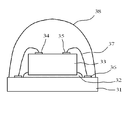
- a light-emitting device using a light-emitting diode (LED) element is widely used, and the structure of an old-type light-emitting device is such that an LED element 33 is bonded onto a substrate 31 with a die bond adhesive 32 as shown in FIG.
- the p electrode 34 and the n electrode 35 on the upper surface are wire-bonded to the connection terminal 36 of the substrate 31 with a gold wire 37, and the entire LED element 33 is sealed with a transparent mold resin 38.
- the gold wire absorbs light having a wavelength of 400 to 500 nm emitted from the LED element 33 to the upper surface side, and a part of the light emitted to the lower surface side is emitted.
- the luminous efficiency of the LED element 33 is reduced by being absorbed by the die bond adhesive 32.
- the light reflecting layer 40 must be provided on the LED element 33 by a metal vapor deposition method or the like so that the p-electrode 34 and the n-electrode 35 are insulated from each other. There was a problem that it was not possible.
- the surface of the conductive particles covered with gold, nickel or copper in the cured anisotropic conductive paste or anisotropic conductive film is brown to dark brown, and
- the epoxy resin binder itself in which the conductive particles are dispersed is also brown due to the imidazole-based latent curing agent commonly used for curing, and the light emission efficiency of the light emitted from the light emitting element (light extraction efficiency) ) Is difficult to improve, and the color of light (light emission color) cannot be reflected as it is.
- An object of the present invention is to solve the above-described problems of the prior art, and light-emitting elements such as light-emitting diodes (LEDs) are flip-chip mounted on a wiring board using an anisotropic conductive adhesive to emit light.
- LEDs light-emitting diodes
- the LED element does not have a light reflection layer that increases the manufacturing cost, and the light emission efficiency is not lowered.
- an anisotropic conductive adhesive containing the same and a light-emitting device in which a light-emitting element is flip-chip mounted on a wiring board using the adhesive.
- the present inventor can avoid reducing the luminous efficiency, on the surface of the conductive particles to be blended in the anisotropic conductive adhesive, By providing a white to gray light reflecting layer made of specific inorganic particles so as not to fall below a specific coverage, the light emission efficiency of the light emitting element and the reflected light color of the conductive particles are reduced.
- the present inventors have found that a hue difference can be prevented during this period, and have completed the present invention.
- the present invention is a light-reflective conductive particle for an anisotropic conductive adhesive used for anisotropic conductive connection of a light emitting element to a wiring board, the core particle coated with a metal material,
- a light-reflective conductive particle comprising a light-reflective layer formed of light-reflective inorganic particles having a refractive index of 1.52 or more on a surface thereof, and a covering ratio of the light-reflective layer on the surface of the core particle being 70% or more.
- the present invention also provides an anisotropic conductive adhesive for use in anisotropic conductive connection of a light emitting element to a wiring board, wherein the light reflective conductive particles described above are applied to visible light having a wavelength of 380 to 780 nm.
- An anisotropic conductive adhesive is provided which is dispersed in a thermosetting resin composition that gives a cured product having an optical path length of 1 cm and a light transmittance (JIS K7105) of 80% or more.
- the present invention provides a light emitting device in which a light emitting element is mounted on a wiring board by a flip chip method through the above-mentioned anisotropic conductive adhesive.
- the light-reflective conductive particles of the present invention for anisotropic conductive adhesive used for anisotropic conductive connection of a light-emitting element to a wiring board are composed of core particles coated with a metal material and a refractive index on the surface thereof. Is composed of a white to gray light reflecting layer formed of light reflecting inorganic particles having a particle size of 1.52 or more, and the coverage of the surface of the core particles by the light reflecting layer is 70% or more. It is.
- the anisotropic conductive adhesive of the present invention is a cured product in which the light-reflective conductive particles have a light transmittance (JIS K7105) of 80% or more with an optical path length of 1 cm with respect to visible light having a wavelength of 380 to 780 nm. It is made to disperse
- JIS K7105 light transmittance
- the light emitting device obtained by flip-chip mounting the light emitting element on the wiring board using the anisotropic conductive adhesive layer of the present invention does not cause coloring even when the anisotropic conductive adhesive is cured, and contains Since the light-reflecting conductive particles that are used have a small wavelength dependency of the reflection property with respect to visible light, the light emission efficiency is improved and the light emission color of the light-emitting element can be reflected as it is.
- FIG. 1A and 1B are cross-sectional views of the light-reflective conductive particles 10 and 20 of the present invention for an anisotropic conductive adhesive. First, the light reflective conductive particles in FIG. 1A will be described.
- the light-reflective conductive particle 10 includes a core particle 1 coated with a metal material and a light-reflecting layer 3 formed on the surface of the light-reflective inorganic particle 2 having a refractive index of 1.52 or more. .
- the light-reflective inorganic particles 2 having a refractive index of 1.52 or more are inorganic particles that exhibit white under sunlight. Accordingly, the light reflecting layer 3 formed from them exhibits white to gray.
- the expression of white to gray means that the wavelength dependency of the reflection characteristic for visible light is small and the visible light is easily reflected.
- Preferred examples of the light reflecting inorganic particles 2 include at least one selected from titanium oxide (TiO 2 ) particles, zinc oxide (ZnO) particles, and aluminum oxide (Al 2 O 3 ) particles.
- titanium oxide particles titanium oxide particles, zinc oxide particles, or aluminum oxide particles, if there is a concern about photodegradation of a cured product of a cured thermosetting resin of an anisotropic conductive adhesive, it is catalytic to photodegradation.
- Zinc oxide having a high refractive index can be preferably used.
- the core particle 1 Since the core particle 1 is subjected to anisotropic conductive connection, its surface is made of a metal material.
- the surface is coated with a metal material, an aspect in which the core particle 1 itself is a metal material, or an aspect in which the surface of the resin particle is coated with a metal material can be given.
- a metal material used in conventional conductive particles for anisotropic conductive connection can be used.
- examples thereof include gold, nickel, copper, silver, solder, palladium, aluminum, alloys thereof, multilayered products thereof (for example, nickel plating / gold flash plating products), and the like. Above all, gold, nickel, and copper turn the conductive particles brown, so that the effects of the present invention can be enjoyed over other metal materials.
- the resin particle portion of the metal-coated resin particle conventionally used as the conductive particle for anisotropic conductive connection is used as the resin particle.
- resin particles include styrene resin particles, benzoguanamine resin particles, and nylon resin particles.
- a method of coating the resin particles with a metal material a conventionally known method can be employed, and an electroless plating method, an electrolytic plating method, or the like can be used.
- the layer thickness of the metal material to be coated is sufficient to ensure good connection reliability, and is usually 0.1 to 3 ⁇ m, preferably depending on the particle size of the resin particles and the type of metal. 0.1 to 1 ⁇ m.
- the particle size of the core particle 1 having a metal material surface is too small, conduction will be poor, and if it is too large, a short circuit between patterns tends to occur. Therefore, it is preferably 1 to 20 ⁇ m, more preferably 3 to 5 ⁇ m, particularly preferably. 3 to 5 ⁇ m.
- the shape of the core particle 1 is preferably a spherical shape, but may be a flake shape or a rugby ball shape.
- the layer thickness of the light reflecting layer 3 formed from the light reflecting inorganic particles 2 is too small with respect to the particle size of the core particle 1 from the viewpoint of the relative size with respect to the particle size of the core particle 1, it is reflected.
- the rate decreases, and if it is too large, there is a tendency for poor conduction, so the content is preferably 0.5 to 50%, more preferably 1 to 25%.
- the light-reflecting inorganic particles 2 constituting the light-reflecting layer 3 have a particle size that is too small to cause the light-reflecting phenomenon, and if it is too large, it is difficult to form the light-reflecting layer. Therefore, it is preferably 0.02 to 4 ⁇ m, more preferably 0.1 to 1 ⁇ m, and particularly preferably 0.2 to 0.5 ⁇ m.
- the particle size of the light-reflecting inorganic particles 2 is such that the light to be reflected (that is, the light emitted from the light emitting element) is not transmitted. It is preferable that it is 50% or more of the wavelength.
- examples of the shape of the light-reflective inorganic particles 2 include an amorphous shape, a spherical shape, a scale shape, and a needle shape. Among them, a spherical shape from the viewpoint of the light diffusion effect, and a scale shape from the point of the total reflection effect. Shape is preferred.
- the light-reflective conductive particles 10 in FIG. 1A are formed by a known film forming technique (so-called mechano-fusion method) in which a film composed of small-sized particles is formed on the surface of large-sized particles by physically colliding large and small powders. ).
- the light-reflective inorganic particles 2 are fixed so as to bite into the metal material on the surface of the core particle 1.
- the inorganic particles are hardly fused and fixed, the monolayer of the inorganic particles forms the light-reflective layer 3.
- the layer thickness of the light reflecting layer 3 is considered to be equivalent to or slightly thinner than the particle size of the light reflecting inorganic particles 2.
- the light reflective conductive particles 20 in FIG. 1B will be described.
- the light-reflective layer 3 contains a thermoplastic resin 4 that functions as an adhesive, and the light-reflective inorganic particles 2 are fixed to each other by the thermoplastic resin 4. 2 differs from the light-reflective conductive particle 10 in FIG. 1A in that it is multilayered (for example, multilayered into two or three layers). By including such a thermoplastic resin 4, the mechanical strength of the light reflecting layer 3 is improved, and the inorganic particles are less likely to be peeled off.
- the light reflective conductive particle 20 of FIG. 1B can be manufactured by a mechano-fusion method.
- a particulate thermoplastic resin 4 may be used in combination.
- the light reflective conductive particle 20 of FIG. 1B is also manufactured simultaneously.
- thermoplastic resin 4 a halogen-free thermoplastic resin can be preferably used for the purpose of reducing the environmental load, and for example, polyolefins such as polyethylene and polypropylene, polystyrene, acrylic resins, and the like can be preferably used. .
- Such light-reflective conductive particles 20 can also be manufactured by a mechanofusion method. If the particle size of the thermoplastic resin 4 applied to the mechano-fusion method is too small, the effect as an adhesive is small, and if it is too large, it is difficult to adhere to the core particle 1, so that it is preferably 0.02 to 4 ⁇ m, more preferably 0.1 to 1 ⁇ m. Further, if the blending amount of the thermoplastic resin 4 is too small, the effect as an adhesive is small, and if it is too large, an unintended particle aggregate is generated. Therefore, with respect to 100 parts by mass of the core particle 1, The amount is preferably 0.2 to 500 parts by mass, more preferably 4 to 25 parts by mass.
- the coverage is 70% or more, preferably 80% or more.
- the covering ratio is measured by arranging the light-reflective conductive particles on the pressure-sensitive adhesive tape so as to form a single-layer particle layer, and capturing a 100-fold enlarged planar image obtained by a CCD camera into a personal computer.
- the image processing software can perform the calculation by calculating an average coverage based on a predetermined binarization process (a process for converting a grayscale image into a binary image) (coverage measurement method A).
- 30 conductive particles arbitrarily selected with a scanning electron microscope are enlarged (for example, 8000 times), and for each conductive particle, a covering state with attached insulating particles is sketched in a plane, It can also be performed by calculating an average coverage of 30 pieces (coverage measurement method B). Or it can also carry out by empirically judging that it has coat
- the core particle having a surface made of gold, nickel or copper has a brown surface color, whereas such a core particle can be observed in gray.
- a criterion is that the coverage is 70% or more.
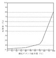
- titanium oxide powder having an average particle size of 0.5 ⁇ m is added to the thermosetting epoxy binder composition used in the thermosetting epoxy binder composition used in Example 1 of the present specification. Dry the paint uniformly mixed in such an amount that the ratio of the titanium oxide powder to the total of the titanium oxide powder is 0%, 40%, 50%, 60%, 70%, 80%, 90%, 100%.
- a black plate was coated to a thickness of 100 ⁇ m, heated at 200 ° C. for 1 minute to cure, and the resulting cured product was used with a spectrophotometer (U3300, Hitachi, Ltd.), wavelength 450 nm.
- the reflectance (JIS K7105) with respect to light is measured, the reflectance curve of FIG. 1C is obtained. From FIG. 1C, it is observed that the ratio of the titanium oxide powder to the total of the thermosetting epoxy binder composition and the titanium oxide powder increases sharply at 70%.
- This anisotropic conductive adhesive is obtained by dispersing the light-reflective conductive particles of the present invention in a thermosetting resin composition, and can take a form such as a paste or a film.
- thermosetting resin composition used for the anisotropic conductive adhesive of the present invention it is preferable to use a transparent and colorless one as much as possible. This is because the light reflecting efficiency of the light-reflective conductive particles in the anisotropic conductive adhesive is reflected without decreasing, and the light color of incident light is not changed.
- colorless and transparent means that the cured product of the anisotropic conductive adhesive has a light transmittance (JIS K7105) of 80% or more, preferably 90% or more with respect to visible light having a wavelength of 380 to 780 nm.
- the amount of the light-reflective conductive particles with respect to 100 parts by mass of the thermosetting resin composition is preferably 1 to 100 parts by mass, more preferably 10 to 50 parts by mass.
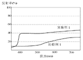
- the reflective property of the anisotropic conductive adhesive of the present invention is that the reflectance (JIS K7105) of light having a wavelength of 450 nm of a 100 ⁇ m-thick cured product of the anisotropic conductive adhesive is improved in order to improve the light emission efficiency of the light emitting element. , Preferably at least 15%.
- the reflection characteristics and blending amount of the light-reflective conductive particles to be used, the blending composition of the thermosetting resin composition, and the like may be appropriately adjusted. Usually, if the amount of the light-reflective conductive particles having good reflection characteristics is increased, the reflectance tends to increase.
- the reflective property of the anisotropic conductive adhesive can be evaluated from the viewpoint of refractive index (JIS K7142). That is, if the refractive index difference between the thermosetting resin composition of the anisotropic conductive adhesive and the light-reflective conductive particles is too large, the light-reflective conductive particles and the thermosetting resin composition surrounding the light-reflective conductive particles This is because the amount of light reflection at the interface with the cured product increases. Specifically, it is desired that the difference in refractive index between the thermosetting resin composition and the light-reflecting inorganic particles is 0.02 or more, preferably 0.3 or more. In general, the refractive index of a thermosetting resin composition mainly composed of an epoxy resin is about 1.5.
- thermosetting resin composition constituting the anisotropic conductive adhesive of the present invention
- those used in conventional anisotropic conductive adhesives and anisotropic conductive films can be used.
- a thermosetting resin composition is obtained by blending a curing agent with an insulating binder resin.
- the insulating binder resin is preferably an epoxy resin mainly composed of an alicyclic epoxy resin, a heterocyclic epoxy compound, a hydrogenated epoxy resin, or the like.
- Preferred examples of the alicyclic epoxy compound include those having two or more epoxy groups in the molecule. These may be liquid or solid. Specific examples include glycidyl hexahydrobisphenol A, 3,4-epoxycyclohexenylmethyl-3 ′, 4′-epoxycyclohexene carboxylate, and the like. Among these, glycidyl hexahydrobisphenol A, 3,4-epoxycyclohexenylmethyl-3 ′, 4 is preferable because it can ensure light transmission suitable for mounting LED elements on the cured product and is excellent in rapid curing. '-Epoxycyclohexenecarboxylate can be preferably used.
- heterocyclic epoxy compound examples include an epoxy compound having a triazine ring, and 1,3,5-tris (2,3-epoxypropyl) -1,3,5-triazine-2,4 is particularly preferable. , 6- (1H, 3H, 5H) -trione.
- hydrogenated epoxy compound hydrogenated products of the above-described alicyclic epoxy compounds and heterocyclic epoxy compounds, and other known hydrogenated epoxy resins can be used.
- the alicyclic epoxy compound, the heterocyclic epoxy compound and the hydrogenated epoxy compound may be used singly or in combination of two or more.
- other epoxy compounds may be used in combination as long as the effects of the present invention are not impaired.
- an acid anhydride As the curing agent, an acid anhydride, an imidazole compound, dicyan, or the like can be used.
- acid anhydrides that are difficult to discolor the cured product particularly alicyclic acid anhydride-based curing agents, can be preferably used.
- methylhexahydrophthalic anhydride (MeHHPA) or the like can be preferably used.
- thermosetting resin composition of the anisotropic conductive adhesive of the present invention when an alicyclic epoxy compound and an alicyclic acid anhydride-based curing agent are used, the respective amounts used are alicyclic acid anhydrides. If the amount of the physical curing agent is too small, the amount of uncured epoxy compound increases, resulting in poor curing. If the amount is too large, the corrosion of the adherend material tends to be accelerated by the influence of the excess curing agent.
- the alicyclic acid anhydride curing agent is preferably used in an amount of 80 to 120 parts by weight, more preferably 95 to 105 parts by weight, based on 100 parts by weight of the compound.
- the anisotropic conductive adhesive of the present invention can be produced by uniformly mixing light-reflective conductive particles and a thermosetting resin composition. Also, when using anisotropic conductive adhesives as anisotropic conductive films, they are dispersed and mixed together with a solvent such as toluene, and applied to the peeled PET film so as to have the desired thickness. What is necessary is just to dry at the temperature of about 80 degreeC.
- the light-emitting device 200 includes the connection terminal 22 on the substrate 21 and the connection bumps 26 formed on the n-electrode 24 and the p-electrode 25 of the LED element 23 as light-emitting elements.
- an anisotropic conductive adhesive is applied and the substrate 21 and the LED element 23 are flip-chip mounted.
- the cured product 100 of the anisotropic conductive adhesive is obtained by dispersing the light-reflective conductive particles 10 in the cured product 11 of the thermosetting resin composition.
- light emitted from the LED element 23 toward the substrate 21 is light-reflective conductive in the cured product 100 of the anisotropic conductive adhesive. Reflected by the particles 10 and emitted from the upper surface of the LED element 23. Accordingly, it is possible to prevent a decrease in luminous efficiency.
- Example 1 (Creation of light-reflective conductive particles) 4 parts by mass of titanium oxide powder (KR-380, Titanium Industry Co., Ltd.) having an average particle size of 0.5 ⁇ m and Au coated resin conductive particles having an average particle size of 5 ⁇ m with a brown appearance color (spherical shape having an average particle size of 4.6 ⁇ m) Particles obtained by electroless gold plating of 0.2 ⁇ m thickness on acrylic resin particles: 20 parts by weight of Bright 20GNB4.6EH, Nippon Chemical Industry Co., Ltd. are put into a mechanofusion apparatus (AMS-GMP, Hosokawa Micron Corporation).
- AMS-GMP Hosokawa Micron Corporation
- the light-reflective conductive particles of Example 1 were formed by forming a light-reflective layer made of titanium oxide particles with a thickness of about 0.3 ⁇ m on the surface of the conductive particles under the conditions of a rotation speed of 1000 rpm and a rotation time of 20 minutes. Obtained. The appearance color of the light reflective conductive particles was gray.
- the obtained anisotropic conductive adhesive was applied to a white plate made of ceramic so as to have a dry thickness of 100 ⁇ m, and heated at 200 ° C. for 1 minute to be cured. About this hardened
- a glass epoxy substrate having a wiring obtained by plating Ni / Au (5.0 ⁇ m thickness / 0.3 ⁇ m thickness) on a 50 ⁇ m pitch copper wiring using the anisotropic conductive adhesive prepared in the light reflectance evaluation test. , 15 [mu] m height of the test IC chips 6mm square with gold bumps (conductive connection area / conductor - space 1600 ⁇ m 2 / 50 ⁇ mP) to 200 ° C., and flip chip mounted in 60 seconds, provided that 1Kg / chip, test IC Got a module.
- TCT temperature cycle test
- Example 2 Light whose appearance color is gray as in Example 1, except that the rotation speed of the mechanofusion device (AMS-GMP, Hosokawa Micron Co., Ltd.) is changed from 1000 rpm to 700 rpm and the rotation time is changed from 20 minutes to 10 minutes. Reflective conductive particles were obtained, and an anisotropic conductive adhesive was obtained. Further, in the same manner as in Example 1, the coverage ratio and the reflectance were measured, and further an electrical property (conduction reliability, insulation reliability) evaluation test was performed. The obtained results are shown in Table 1.
- AMS-GMP mechanofusion device
- Example 3 The appearance color was the same as in Example 1 except that Ni coated resin conductive particles (52NR-4.6EH, Nippon Chemical Industry Co., Ltd.) having an average particle size of 5.0 ⁇ m were used instead of Au coated resin conductive particles. Obtained gray light-reflective conductive particles, and an anisotropic conductive adhesive was obtained. Further, in the same manner as in Example 1, the coverage ratio and the reflectance were measured, and further an electrical property (conduction reliability, insulation reliability) evaluation test was performed. The obtained results are shown in Table 1.
- Ni coated resin conductive particles 52NR-4.6EH, Nippon Chemical Industry Co., Ltd.
- Example 4 4 parts by mass of titanium oxide powder (KR-380, Titanium Industry Co., Ltd.) having an average particle size of 0.5 ⁇ m and polystyrene (PS) particles (Grossdale 204S, Mitsui Chemicals, Inc.) having an average particle size of 0.2 ⁇ m as adhesive particles Co., Ltd.) 3 parts by mass and conductive particles having an average particle size of 5 ⁇ m (particles obtained by subjecting spherical acrylic resin particles having an average particle size of 4.6 ⁇ m to electroless gold plating of 0.2 ⁇ m thickness: Bright 20GNB4.6EH, Nippon Chemical Industry ( 20 parts by mass into a mechanofusion apparatus (AMS-GMP, Hosokawa Micron Corporation), and on the surface of the conductive particles under the conditions of a rotation speed of 1000 rpm and a rotation time of 20 minutes, styrene and titanium oxide particles By forming a light reflection layer having a thickness of about 1 ⁇ m, light reflective conductive particles having a gray
- Example 5 External color as in Example 3 except that Ni coated resin conductive particles (52NR-4.6EH, Nippon Chemical Industry Co., Ltd.) having an average particle size of 5.0 ⁇ m were used instead of Au coated resin conductive particles. Obtained gray light-reflective conductive particles, and an anisotropic conductive adhesive was obtained. Further, similarly to Example 1, the coverage and reflectance were measured, and further an electrical property (conduction reliability, insulation reliability) evaluation test was performed. The obtained results are shown in Table 1.
- Example 6 Use polyethylene (PE) particles (Amipearl WF300, Mitsui Chemicals) with an average particle size of 0.2 ⁇ m instead of polystyrene particles (Grossdale 204S, Mitsui Chemicals, Inc.) with an average particle size of 0.2 ⁇ m.
- PE polyethylene
- Example 3 Light-reflective conductive particles having a gray appearance color were obtained, and an anisotropic conductive adhesive was further obtained. Further, in the same manner as in Example 1, the coverage ratio and the reflectance were measured, and further an electrical property (conduction reliability, insulation reliability) evaluation test was performed. The obtained results are shown in Table 1.
- Example 7 The appearance color was the same as in Example 3 except that instead of the titanium oxide powder having an average particle diameter of 0.5 ⁇ m, zinc oxide powder having an average particle diameter of 0.5 ⁇ m (one type of zinc oxide, Hakusuitec Co., Ltd.) was used. Obtained gray light-reflective conductive particles, and an anisotropic conductive adhesive was obtained. Further, in the same manner as in Example 1, the coverage ratio and the reflectance were measured, and further an electrical property (conduction reliability, insulation reliability) evaluation test was performed. The obtained results are shown in Table 1.
- Example 8 The appearance color was the same as in Example 3 except that aluminum oxide powder (AE-2500SI, Admatechs Co., Ltd.) having an average particle diameter of 0.5 ⁇ m was used instead of titanium oxide powder having an average particle diameter of 0.5 ⁇ m. Obtained gray light-reflective conductive particles, and an anisotropic conductive adhesive was obtained. Further, in the same manner as in Example 1, the coverage ratio and the reflectance were measured, and further an electrical property (conduction reliability, insulation reliability) evaluation test was performed. The obtained results are shown in Table 1.
- aluminum oxide powder AE-2500SI, Admatechs Co., Ltd.
- Example 9 Instead of titanium oxide powder having an average particle diameter of 0.5 ⁇ m, light-reflective conductive particles having a gray appearance color were obtained in the same manner as in Example 3 except that magnesium carbonate having an average particle diameter of 0.5 ⁇ m was used. An anisotropic conductive adhesive was obtained. Further, in the same manner as in Example 1, the coverage ratio and the reflectance were measured, and further an electrical property (conduction reliability, insulation reliability) evaluation test was performed. The obtained results are shown in Table 1.
- Example 10 The appearance color is gray in the same manner as in Example 3 except that titanium oxide powder having an average particle diameter of 0.2 ⁇ m (JR405, Teika) is used instead of titanium oxide powder having an average particle diameter of 0.5 ⁇ m. Light-reflective conductive particles were obtained, and further an anisotropic conductive adhesive was obtained. Further, in the same manner as in Example 1, the coverage ratio and the reflectance were measured, and further an electrical property (conduction reliability, insulation reliability) evaluation test was performed. The obtained results are shown in Table 1.
- Comparative Example 1 Using Au coated resin conductive particles having a brown appearance color (particles obtained by electroless gold plating of 0.2 ⁇ m thickness on spherical acrylic resin particles having an average particle diameter of 4.6 ⁇ m: Bright 20GNB4.6EH, Nippon Chemical Industry Co., Ltd.) An anisotropic conductive adhesive was obtained in the same manner as in Example 1. Further, in the same manner as in Example 1, the reflectance was measured, and further an electrical property (conduction reliability, insulation reliability) evaluation test was performed. The obtained results are shown in Table 1.
- Comparative Example 2 Comparative Example 1 except that instead of the Au-coated resin conductive particles, Ni-coated resin conductive particles (52NR-4.6EH, Nippon Chemical Industry Co., Ltd.) having a brown appearance color and an average particle diameter of 5.0 ⁇ m are used. Similarly, an anisotropic conductive adhesive was obtained. Further, in the same manner as in Example 1, the reflectance was measured, and further an electrical property (conduction reliability, insulation reliability) evaluation test was performed. The obtained results are shown in Table 1.
- Comparative Example 3 3 parts by mass of polystyrene-based particles (Grossdale 204S, Mitsui Chemicals, Inc.) with an average particle size of 0.2 ⁇ m and conductive particles with an average particle size of 5 ⁇ m (spherical acrylic resin particles with an average particle size of 4.6 ⁇ m are 0.2 ⁇ m thick) Electroless gold-plated particles: Bright 20GNB4.6EH, Nippon Kagaku Kogyo Co., Ltd.
- Comparative Example 4 Instead of titanium oxide powder with an average particle size of 0.5 ⁇ m, use silicon oxide (silica) powder (Seahoster KEP-30, Nippon Shokubai Co., Ltd.) with a refractive index of 1.45 and an average particle size of 0.5 ⁇ m. Otherwise, conductive particles having a brown appearance color were obtained in the same manner as in Example 3, and further an anisotropic conductive adhesive was obtained. Further, in the same manner as in Example 1, the coverage ratio and the reflectance were measured, and further an electrical property (conduction reliability, insulation reliability) evaluation test was performed. The obtained results are shown in Table 1.
- the anisotropic conductive adhesives using the light-reflective conductive particles of Examples 1 to 10 have a coverage by the light-reflective layer of 70% or more, and the light reflectivities are all 15% or more. Yes, the blue color of 450 nm light was reflected as it was. In addition, the conduction reliability and the insulation reliability were also good results.
- the light-reflective conductive particle of the present invention increases the manufacturing cost when a light-emitting device is manufactured by flip-chip mounting a light-emitting element such as a light-emitting diode (LED) element on a wiring board using an anisotropic conductive adhesive.
- a light-emitting element such as a light-emitting diode (LED) element
- the anisotropic conductive adhesive of the present invention is useful when the LED element is flip-chip mounted.
Landscapes
- Engineering & Computer Science (AREA)
- Chemical & Material Sciences (AREA)
- Microelectronics & Electronic Packaging (AREA)
- Organic Chemistry (AREA)
- Computer Hardware Design (AREA)
- Power Engineering (AREA)
- Manufacturing & Machinery (AREA)
- Physics & Mathematics (AREA)
- Dispersion Chemistry (AREA)
- Spectroscopy & Molecular Physics (AREA)
- Medicinal Chemistry (AREA)
- Polymers & Plastics (AREA)
- Chemical Kinetics & Catalysis (AREA)
- Health & Medical Sciences (AREA)
- Inorganic Chemistry (AREA)
- Adhesives Or Adhesive Processes (AREA)
- Led Device Packages (AREA)
- Conductive Materials (AREA)
- Powder Metallurgy (AREA)
- Non-Insulated Conductors (AREA)
Abstract
Description
(光反射性導電粒子の作成)
平均粒子径0.5μmの酸化チタン粉末(KR-380、チタン工業(株))4質量部と、外観色が茶色の平均粒径5μmのAu被覆樹脂導電粒子(平均粒径4.6μmの球状アクリル樹脂粒子に0.2μm厚の無電解金メッキを施した粒子:ブライト20GNB4.6EH、日本化学工業(株))20質量部とを、メカノフュージョン装置(AMS-GMP、ホソカワミクロン(株))に投入し、回転速度1000rpm、回転時間20分という条件で導電粒子の表面に、酸化チタン粒子からなる約0.3μm厚の光反射層を成膜することにより、実施例1の光反射性導電粒子を得た。この光反射性導電粒子の外観色は灰色であった。
得られた光反射性粒子の光反射層による被覆率を、前述した被覆率測定B法に従って測定した。得られた結果を表1に示す。
得られた光反射性導電粒子15質量部と、屈折率が約1.5の無色透明な熱硬化型エポキシ系バインダー組成物(YX-8000、JER(株))100質量部とを真空脱泡撹拌装置を用いて均一に混合することにより、実施例1の異方性導電接着剤を得た。
光反射率評価試験の際に調製した異方性導電接着剤を用いて、50μmピッチの銅配線にNi/Au(5.0μm厚/0.3μm厚)メッキ処理した配線を有するガラスエポキシ基板に、15μm高の金バンプを有する6mm角の試験用ICチップ(導体接続面積/導体-スペース=1600μm2/50μmP)を200℃、60秒、1Kg/チップという条件でフィリップチップ実装し、テスト用ICモジュールを得た。
得られたテスト用ICモジュールに対し、低温(-40℃)と高温(100℃)の温度に交互に加熱・冷却する温度サイクル試験(TCT)(JIS C5030)を行い、初期と500サイクル後の4端子法による抵抗値を測定した。抵抗値が1Ω未満の場合を良好「○」と評価し、1Ω以上となった場合を不良「×」と評価した。得られた結果を表1に示す。
別途作成したテスト用ICモジュールに対し、85℃、85%RHの環境下に1000時間放置というエージング試験を行い、初期と1000時間後の抵抗値を測定した。抵抗値が106Ω以上の場合を良好「○」と評価し、106Ω未満となった場合を不良「×」と評価した。得られた結果を表1に示す。
メカノフュージョン装置(AMS-GMP、ホソカワミクロン(株))の回転速度を1000rpmから700rpmに変更し且つ回転時間を20分から10分に変更すること以外、実施例1と同様にして外観色が灰色の光反射性導電粒子を得、更に異方性導電接着剤を得た。また、実施例1と同様に、被覆率及び反射率を測定し、更に電気特性(導通信頼性、絶縁信頼性)評価試験を行った。得られた結果を表1に示す。
Au被覆樹脂導電粒子に代えて、平均粒子径5.0μmのNi被覆樹脂導電粒子(52NR-4.6EH、日本化学工業(株))を使用すること以外、実施例1と同様にして外観色が灰色の光反射性導電粒子を得、更に異方性導電接着剤を得た。また、実施例1と同様に、被覆率及び反射率を測定し、更に電気特性(導通信頼性、絶縁信頼性)評価試験を行った。得られた結果を表1に示す。
平均粒子径0.5μmの酸化チタン粉末(KR-380、チタン工業(株))4質量部と、接着剤粒子として平均粒子径0.2μmのポリスチレン(PS)粒子(グロスデール204S、三井化学(株))3質量部と、平均粒径5μmの導電粒子(平均粒径4.6μmの球状アクリル樹脂粒子に0.2μm厚の無電解金メッキを施した粒子:ブライト20GNB4.6EH、日本化学工業(株))20質量部とを、メカノフュージョン装置(AMS-GMP、ホソカワミクロン(株))に投入し、回転速度1000rpm、回転時間20分という条件で導電粒子の表面に、スチレンと酸化チタン粒子とからなる約1μm厚の光反射層を成膜することにより、外観色が灰色の光反射性導電粒子を得、更に異方性導電接着剤を得た。また、実施例1と同様に、被覆率及び反射率を測定し、更に電気特性(導通信頼性、絶縁信頼性)評価試験を行った。得られた結果を表1に示す。
Au被覆樹脂導電粒子に代えて、平均粒子径5.0μmのNi被覆樹脂導電粒子(52NR-4.6EH、日本化学工業(株))を使用すること以外、実施例3と同様にして外観色が灰色の光反射性導電粒子を得、更に異方性導電接着剤を得た。また、更に、実施例1と同様に、被覆率及び反射率を測定し、更に電気特性(導通信頼性、絶縁信頼性)評価試験を行った。得られた結果を表1に示す。
平均粒子径0.2μmのポリスチレン粒子(グロスデール204S、三井化学(株))に代えて、平均粒子径0.2μmのポリエチレン(PE)粒子(アミパールWF300、三井化学(株))を使用すること以外、実施例3と同様にして外観色が灰色の光反射性導電粒子を得、更に異方性導電接着剤を得た。また、実施例1と同様に、被覆率及び反射率を測定し、更に電気特性(導通信頼性、絶縁信頼性)評価試験を行った。得られた結果を表1に示す。
平均粒子径0.5μmの酸化チタン粉末に代えて、平均粒子径0.5μmの酸化亜鉛粉末(酸化亜鉛1種、ハクスイテック(株))を使用すること以外、実施例3と同様にして外観色が灰色の光反射性導電粒子を得、更に異方性導電接着剤を得た。また、実施例1と同様に、被覆率及び反射率を測定し、更に電気特性(導通信頼性、絶縁信頼性)評価試験を行った。得られた結果を表1に示す。
平均粒子径0.5μmの酸化チタン粉末に代えて、平均粒子径0.5μmの酸化アルミニウム粉末(AE-2500SI、(株)アドマテックス)を使用すること以外、実施例3と同様にして外観色が灰色の光反射性導電粒子を得、更に異方性導電接着剤を得た。また、実施例1と同様に、被覆率及び反射率を測定し、更に電気特性(導通信頼性、絶縁信頼性)評価試験を行った。得られた結果を表1に示す。
平均粒子径0.5μmの酸化チタン粉末に代えて、平均粒子径0.5μmの炭酸マグネシウムを使用すること以外、実施例3と同様にして外観色が灰色の光反射性導電粒子を得、更に異方性導電接着剤を得た。また、実施例1と同様に、被覆率及び反射率を測定し、更に電気特性(導通信頼性、絶縁信頼性)評価試験を行った。得られた結果を表1に示す。
平均粒子径0.5μmの酸化チタン粉末に代えて、平均粒子径0.2μmの酸化チタン粉末(JR405、テイカ(株))を使用すること以外、実施例3と同様にして外観色が灰色の光反射性導電粒子を得、更に異方性導電接着剤を得た。また、実施例1と同様に、被覆率及び反射率を測定し、更に電気特性(導通信頼性、絶縁信頼性)評価試験を行った。得られた結果を表1に示す。
外観色が茶色のAu被覆樹脂導電粒子(平均粒径4.6μmの球状アクリル樹脂粒子に0.2μm厚の無電解金メッキを施した粒子:ブライト20GNB4.6EH、日本化学工業(株))を用い、実施例1と同様に異方性導電接着剤を得た。また、実施例1と同様に、反射率を測定し、更に電気特性(導通信頼性、絶縁信頼性)評価試験を行った。得られた結果を表1に示す。
Au被覆樹脂導電粒子に代えて、外観色が茶色の平均粒子径5.0μmのNi被覆樹脂導電粒子(52NR-4.6EH、日本化学工業(株))を使用すること以外、比較例1と同様に異方性導電接着剤を得た。また、実施例1と同様に、反射率を測定し、更に電気特性(導通信頼性、絶縁信頼性)評価試験を行った。得られた結果を表1に示す。
平均粒子径0.2μmのポリスチレン系粒子(グロスデール204S、三井化学(株))3質量部と、平均粒径5μmの導電粒子(平均粒径4.6μmの球状アクリル樹脂粒子に0.2μm厚の無電解金メッキを施した粒子:ブライト20GNB4.6EH、日本化学工業(株))20質量部とを、メカノフュージョン装置(AMS-GMP、ホソカワミクロン(株))に投入し、回転速度1000rpm、回転時間20分という条件で導電粒子の表面に、0.2μm厚のスチレン層を成膜することにより、外観色が茶色の樹脂被覆導電粒子を得、更に異方性導電接着剤を得た。また、実施例1と同様に、反射率を測定し、更に電気特性(導通信頼性、絶縁信頼性)評価試験を行った。得られた結果を表1に示す。
平均粒子径0.5μmの酸化チタン粉末に代えて、屈折率が1.45で平均粒子径0.5μmの酸化ケイ素(シリカ)粉末(シーホスターKEP-30、(株)日本触媒)を使用すること以外、実施例3と同様にして外観色が茶色の導電粒子を得、更に異方性導電接着剤を得た。また、実施例1と同様に、被覆率及び反射率を測定し、更に電気特性(導通信頼性、絶縁信頼性)評価試験を行った。得られた結果を表1に示す。

2 光反射性無機粒子
3 光反射層
4 熱可塑性樹脂
10、20 光反射性導電粒子
11 熱硬化性樹脂組成物の硬化物
21 基板
22 接続端子
23 LED素子
24 n電極
25 p電極
26 バンプ
100 異方性導電接着剤の硬化物
200 発光装置
Claims (15)
- 発光素子を配線板に異方性導電接続するために使用する異方性導電接着剤用の光反射性導電粒子であって、金属材料で被覆されているコア粒子と、その表面に屈折率が1.52以上の光反射性無機粒子から形成された光反射層とからなり、該コア粒子表面の光反射層による被覆率が70%以上である光反射性導電粒子。
- コア粒子を被覆する金属材料が、金、ニッケル又は銅である請求項1記載の光反射性導電粒子。
- コア粒子そのものが、金、ニッケル又は銅の粒子である請求項1記載の光反射性導電粒子。
- コア粒子が、樹脂粒子を金、ニッケル又は銅で被覆したものである請求項1又は2記載の光反射性導電粒子。
- コア粒子の粒子径が1~20μmであり、光反射層の層厚がコア粒子径の0.5~50%である請求項1~4のいずれかに記載の光反射性導電粒子。
- 光反射性無機粒子が、酸化チタン粒子、酸化亜鉛粒子又は酸化アルミニウム粒子から選択された少なくとも一種の無機粒子である請求項1~5のいずれかに記載の光反射性導電粒子。
- 光反射層が、熱可塑性樹脂を含有する請求項1~6のいずれかに記載の光反射性導電粒子。
- 熱可塑性樹脂が、ポリオレフィンである請求項7記載の光反射性導電粒子。
- 発光素子を配線板に異方性導電接続するために使用する異方性導電接着剤であって、請求項1~8のいずれかに記載の光反射性導電粒子を、波長380~750nmの可視光に対して光路長1cmの光透過率(JIS K7105)が80%以上である硬化物を与える熱硬化性樹脂組成物に分散させてなる異方性導電接着剤。
- 熱硬化性樹脂組成物100質量部に対する光反射性導電粒子の配合量が、1~100質量部である請求項9記載の異方性導電接着剤。
- 異方性導電接着剤の100μm厚の硬化物の波長450nmの光に対する反射率(JIS K7105)が、少なくとも15%である請求項9又は10記載の異方性導電接着剤。
- 熱硬化性樹脂組成物と光反射性無機粒子との間の屈折率の差が0.02以上である請求項9~11のいずれかに記載の異方性導電接着剤。
- 熱硬化性樹脂組成物が、エポキシ樹脂と酸無水物系硬化剤とを含有する請求項9~12のいずれかに記載の異方性導電接着剤。
- 請求項9~13のいずれかに記載の異方性導電接着剤を介して、発光素子をフリップチップ方式で配線板に実装されている発光装置。
- 発光素子が、発光ダイオードである請求項14記載の発光装置。
Priority Applications (5)
| Application Number | Priority Date | Filing Date | Title |
|---|---|---|---|
| US13/575,786 US20130105841A1 (en) | 2011-04-20 | 2011-04-20 | Light-reflective conductive particle, anisotropic conductive adhesive, and light-emitting device |
| JP2012534453A JPWO2012144033A1 (ja) | 2011-04-20 | 2011-04-20 | 光反射性導電粒子、異方性導電接着剤及び発光装置 |
| PCT/JP2011/059724 WO2012144033A1 (ja) | 2011-04-20 | 2011-04-20 | 光反射性導電粒子、異方性導電接着剤及び発光装置 |
| TW100128832A TWI517456B (zh) | 2011-04-20 | 2011-08-12 | Light reflective conductive particles, anisotropic conductive adhesives and light-emitting devices |
| US14/222,249 US8975654B2 (en) | 2011-04-20 | 2014-03-21 | Light-reflective conductive particle, anisotropic conductive adhesive, and light-emitting device |
Applications Claiming Priority (1)
| Application Number | Priority Date | Filing Date | Title |
|---|---|---|---|
| PCT/JP2011/059724 WO2012144033A1 (ja) | 2011-04-20 | 2011-04-20 | 光反射性導電粒子、異方性導電接着剤及び発光装置 |
Related Child Applications (2)
| Application Number | Title | Priority Date | Filing Date |
|---|---|---|---|
| US13/575,786 A-371-Of-International US20130105841A1 (en) | 2011-04-20 | 2011-04-20 | Light-reflective conductive particle, anisotropic conductive adhesive, and light-emitting device |
| US14/222,249 Continuation US8975654B2 (en) | 2011-04-20 | 2014-03-21 | Light-reflective conductive particle, anisotropic conductive adhesive, and light-emitting device |
Publications (1)
| Publication Number | Publication Date |
|---|---|
| WO2012144033A1 true WO2012144033A1 (ja) | 2012-10-26 |
Family
ID=47041183
Family Applications (1)
| Application Number | Title | Priority Date | Filing Date |
|---|---|---|---|
| PCT/JP2011/059724 WO2012144033A1 (ja) | 2011-04-20 | 2011-04-20 | 光反射性導電粒子、異方性導電接着剤及び発光装置 |
Country Status (4)
| Country | Link |
|---|---|
| US (2) | US20130105841A1 (ja) |
| JP (1) | JPWO2012144033A1 (ja) |
| TW (1) | TWI517456B (ja) |
| WO (1) | WO2012144033A1 (ja) |
Cited By (1)
| Publication number | Priority date | Publication date | Assignee | Title |
|---|---|---|---|---|
| JP2017228533A (ja) * | 2017-07-20 | 2017-12-28 | 日本化学工業株式会社 | 被覆導電性粉体、被覆導電性粉体の製造方法、被覆導電性粉体を含む導電性接着剤及び接着構造体 |
Families Citing this family (6)
| Publication number | Priority date | Publication date | Assignee | Title |
|---|---|---|---|---|
| US9053405B1 (en) * | 2013-08-27 | 2015-06-09 | Flextronics Ap, Llc | Printed RFID circuit |
| KR20160061339A (ko) * | 2013-09-26 | 2016-05-31 | 데쿠세리아루즈 가부시키가이샤 | 발광 장치, 이방성 도전 접착제, 발광 장치 제조 방법 |
| US9812625B2 (en) * | 2014-02-18 | 2017-11-07 | Nichia Corporation | Light-emitting device having resin member with conductive particles |
| JP2015153981A (ja) * | 2014-02-18 | 2015-08-24 | 日亜化学工業株式会社 | 発光装置 |
| JP6432416B2 (ja) * | 2014-04-14 | 2018-12-05 | 日亜化学工業株式会社 | 半導体装置 |
| KR20180016499A (ko) * | 2015-06-11 | 2018-02-14 | 이 잉크 캘리포니아 엘엘씨 | 복합 컬러 입자들 |
Citations (4)
| Publication number | Priority date | Publication date | Assignee | Title |
|---|---|---|---|---|
| JP2007123613A (ja) * | 2005-10-28 | 2007-05-17 | Nichia Chem Ind Ltd | 発光装置 |
| JP2007157940A (ja) * | 2005-12-02 | 2007-06-21 | Nichia Chem Ind Ltd | 発光装置および発光装置の製造方法 |
| JP2007258324A (ja) * | 2006-03-22 | 2007-10-04 | Matsushita Electric Ind Co Ltd | 発光装置の製造方法および発光装置 |
| JP2011057917A (ja) * | 2009-09-14 | 2011-03-24 | Sony Chemical & Information Device Corp | 光反射性異方性導電接着剤及び発光装置 |
Family Cites Families (1)
| Publication number | Priority date | Publication date | Assignee | Title |
|---|---|---|---|---|
| JPH11168235A (ja) | 1997-12-05 | 1999-06-22 | Toyoda Gosei Co Ltd | 発光ダイオード |
-
2011
- 2011-04-20 WO PCT/JP2011/059724 patent/WO2012144033A1/ja active Application Filing
- 2011-04-20 US US13/575,786 patent/US20130105841A1/en not_active Abandoned
- 2011-04-20 JP JP2012534453A patent/JPWO2012144033A1/ja active Pending
- 2011-08-12 TW TW100128832A patent/TWI517456B/zh not_active IP Right Cessation
-
2014
- 2014-03-21 US US14/222,249 patent/US8975654B2/en not_active Expired - Fee Related
Patent Citations (4)
| Publication number | Priority date | Publication date | Assignee | Title |
|---|---|---|---|---|
| JP2007123613A (ja) * | 2005-10-28 | 2007-05-17 | Nichia Chem Ind Ltd | 発光装置 |
| JP2007157940A (ja) * | 2005-12-02 | 2007-06-21 | Nichia Chem Ind Ltd | 発光装置および発光装置の製造方法 |
| JP2007258324A (ja) * | 2006-03-22 | 2007-10-04 | Matsushita Electric Ind Co Ltd | 発光装置の製造方法および発光装置 |
| JP2011057917A (ja) * | 2009-09-14 | 2011-03-24 | Sony Chemical & Information Device Corp | 光反射性異方性導電接着剤及び発光装置 |
Cited By (1)
| Publication number | Priority date | Publication date | Assignee | Title |
|---|---|---|---|---|
| JP2017228533A (ja) * | 2017-07-20 | 2017-12-28 | 日本化学工業株式会社 | 被覆導電性粉体、被覆導電性粉体の製造方法、被覆導電性粉体を含む導電性接着剤及び接着構造体 |
Also Published As
| Publication number | Publication date |
|---|---|
| US20130105841A1 (en) | 2013-05-02 |
| TW201246634A (en) | 2012-11-16 |
| US20140225144A1 (en) | 2014-08-14 |
| JPWO2012144033A1 (ja) | 2014-07-28 |
| US8975654B2 (en) | 2015-03-10 |
| TWI517456B (zh) | 2016-01-11 |
Similar Documents
| Publication | Publication Date | Title |
|---|---|---|
| JP5526698B2 (ja) | 光反射性導電粒子、異方性導電接着剤及び発光装置 | |
| JP5617210B2 (ja) | 光反射性異方性導電接着剤及び発光装置 | |
| JP5609716B2 (ja) | 光反射性異方性導電接着剤及び発光装置 | |
| JP5402804B2 (ja) | 発光装置の製造方法 | |
| JP5888023B2 (ja) | 光反射性異方性導電接着剤及び発光装置 | |
| JP5958107B2 (ja) | 光反射性異方性導電接着剤及び発光装置 | |
| JP6347635B2 (ja) | 異方性導電接着剤 | |
| WO2012144033A1 (ja) | 光反射性導電粒子、異方性導電接着剤及び発光装置 | |
| WO2014046089A1 (ja) | 接続構造体の製造方法及び異方性導電接着剤 | |
| JP5555038B2 (ja) | 光反射性異方性導電接着剤及び発光装置 | |
| WO2012127978A1 (ja) | 光反射性異方性導電接着剤及び発光装置 | |
| JP2014030026A (ja) | 異方性導電接着剤及び発光装置 | |
| JP5785306B2 (ja) | 光反射性異方性導電接着剤及び発光装置 |
Legal Events
| Date | Code | Title | Description |
|---|---|---|---|
| ENP | Entry into the national phase |
Ref document number: 2012534453 Country of ref document: JP Kind code of ref document: A |
|
| WWE | Wipo information: entry into national phase |
Ref document number: 13575786 Country of ref document: US |
|
| 121 | Ep: the epo has been informed by wipo that ep was designated in this application |
Ref document number: 11864019 Country of ref document: EP Kind code of ref document: A1 |
|
| NENP | Non-entry into the national phase |
Ref country code: DE |
|
| 122 | Ep: pct application non-entry in european phase |
Ref document number: 11864019 Country of ref document: EP Kind code of ref document: A1 |