WO2012124246A1 - Procédé de production de couche mince et dispositif de production de couche mince - Google Patents
Procédé de production de couche mince et dispositif de production de couche mince Download PDFInfo
- Publication number
- WO2012124246A1 WO2012124246A1 PCT/JP2012/000400 JP2012000400W WO2012124246A1 WO 2012124246 A1 WO2012124246 A1 WO 2012124246A1 JP 2012000400 W JP2012000400 W JP 2012000400W WO 2012124246 A1 WO2012124246 A1 WO 2012124246A1
- Authority
- WO
- WIPO (PCT)
- Prior art keywords
- substrate
- thin film
- cooling material
- main surface
- formation region
- Prior art date
Links
Images


Classifications
-
- H—ELECTRICITY
- H01—ELECTRIC ELEMENTS
- H01M—PROCESSES OR MEANS, e.g. BATTERIES, FOR THE DIRECT CONVERSION OF CHEMICAL ENERGY INTO ELECTRICAL ENERGY
- H01M4/00—Electrodes
- H01M4/02—Electrodes composed of, or comprising, active material
- H01M4/04—Processes of manufacture in general
- H01M4/0402—Methods of deposition of the material
- H01M4/0421—Methods of deposition of the material involving vapour deposition
- H01M4/0423—Physical vapour deposition
- H01M4/0426—Sputtering
-
- C—CHEMISTRY; METALLURGY
- C23—COATING METALLIC MATERIAL; COATING MATERIAL WITH METALLIC MATERIAL; CHEMICAL SURFACE TREATMENT; DIFFUSION TREATMENT OF METALLIC MATERIAL; COATING BY VACUUM EVAPORATION, BY SPUTTERING, BY ION IMPLANTATION OR BY CHEMICAL VAPOUR DEPOSITION, IN GENERAL; INHIBITING CORROSION OF METALLIC MATERIAL OR INCRUSTATION IN GENERAL
- C23C—COATING METALLIC MATERIAL; COATING MATERIAL WITH METALLIC MATERIAL; SURFACE TREATMENT OF METALLIC MATERIAL BY DIFFUSION INTO THE SURFACE, BY CHEMICAL CONVERSION OR SUBSTITUTION; COATING BY VACUUM EVAPORATION, BY SPUTTERING, BY ION IMPLANTATION OR BY CHEMICAL VAPOUR DEPOSITION, IN GENERAL
- C23C14/00—Coating by vacuum evaporation, by sputtering or by ion implantation of the coating forming material
- C23C14/22—Coating by vacuum evaporation, by sputtering or by ion implantation of the coating forming material characterised by the process of coating
- C23C14/24—Vacuum evaporation
-
- C—CHEMISTRY; METALLURGY
- C23—COATING METALLIC MATERIAL; COATING MATERIAL WITH METALLIC MATERIAL; CHEMICAL SURFACE TREATMENT; DIFFUSION TREATMENT OF METALLIC MATERIAL; COATING BY VACUUM EVAPORATION, BY SPUTTERING, BY ION IMPLANTATION OR BY CHEMICAL VAPOUR DEPOSITION, IN GENERAL; INHIBITING CORROSION OF METALLIC MATERIAL OR INCRUSTATION IN GENERAL
- C23C—COATING METALLIC MATERIAL; COATING MATERIAL WITH METALLIC MATERIAL; SURFACE TREATMENT OF METALLIC MATERIAL BY DIFFUSION INTO THE SURFACE, BY CHEMICAL CONVERSION OR SUBSTITUTION; COATING BY VACUUM EVAPORATION, BY SPUTTERING, BY ION IMPLANTATION OR BY CHEMICAL VAPOUR DEPOSITION, IN GENERAL
- C23C14/00—Coating by vacuum evaporation, by sputtering or by ion implantation of the coating forming material
- C23C14/22—Coating by vacuum evaporation, by sputtering or by ion implantation of the coating forming material characterised by the process of coating
- C23C14/54—Controlling or regulating the coating process
- C23C14/541—Heating or cooling of the substrates
-
- C—CHEMISTRY; METALLURGY
- C23—COATING METALLIC MATERIAL; COATING MATERIAL WITH METALLIC MATERIAL; CHEMICAL SURFACE TREATMENT; DIFFUSION TREATMENT OF METALLIC MATERIAL; COATING BY VACUUM EVAPORATION, BY SPUTTERING, BY ION IMPLANTATION OR BY CHEMICAL VAPOUR DEPOSITION, IN GENERAL; INHIBITING CORROSION OF METALLIC MATERIAL OR INCRUSTATION IN GENERAL
- C23C—COATING METALLIC MATERIAL; COATING MATERIAL WITH METALLIC MATERIAL; SURFACE TREATMENT OF METALLIC MATERIAL BY DIFFUSION INTO THE SURFACE, BY CHEMICAL CONVERSION OR SUBSTITUTION; COATING BY VACUUM EVAPORATION, BY SPUTTERING, BY ION IMPLANTATION OR BY CHEMICAL VAPOUR DEPOSITION, IN GENERAL
- C23C14/00—Coating by vacuum evaporation, by sputtering or by ion implantation of the coating forming material
- C23C14/22—Coating by vacuum evaporation, by sputtering or by ion implantation of the coating forming material characterised by the process of coating
- C23C14/56—Apparatus specially adapted for continuous coating; Arrangements for maintaining the vacuum, e.g. vacuum locks
- C23C14/562—Apparatus specially adapted for continuous coating; Arrangements for maintaining the vacuum, e.g. vacuum locks for coating elongated substrates
-
- H—ELECTRICITY
- H01—ELECTRIC ELEMENTS
- H01M—PROCESSES OR MEANS, e.g. BATTERIES, FOR THE DIRECT CONVERSION OF CHEMICAL ENERGY INTO ELECTRICAL ENERGY
- H01M4/00—Electrodes
- H01M4/02—Electrodes composed of, or comprising, active material
- H01M4/13—Electrodes for accumulators with non-aqueous electrolyte, e.g. for lithium-accumulators; Processes of manufacture thereof
- H01M4/139—Processes of manufacture
- H01M4/1395—Processes of manufacture of electrodes based on metals, Si or alloys
-
- Y—GENERAL TAGGING OF NEW TECHNOLOGICAL DEVELOPMENTS; GENERAL TAGGING OF CROSS-SECTIONAL TECHNOLOGIES SPANNING OVER SEVERAL SECTIONS OF THE IPC; TECHNICAL SUBJECTS COVERED BY FORMER USPC CROSS-REFERENCE ART COLLECTIONS [XRACs] AND DIGESTS
- Y02—TECHNOLOGIES OR APPLICATIONS FOR MITIGATION OR ADAPTATION AGAINST CLIMATE CHANGE
- Y02E—REDUCTION OF GREENHOUSE GAS [GHG] EMISSIONS, RELATED TO ENERGY GENERATION, TRANSMISSION OR DISTRIBUTION
- Y02E60/00—Enabling technologies; Technologies with a potential or indirect contribution to GHG emissions mitigation
- Y02E60/10—Energy storage using batteries
Landscapes
- Chemical & Material Sciences (AREA)
- Engineering & Computer Science (AREA)
- Chemical Kinetics & Catalysis (AREA)
- Materials Engineering (AREA)
- Organic Chemistry (AREA)
- Mechanical Engineering (AREA)
- Metallurgy (AREA)
- Electrochemistry (AREA)
- General Chemical & Material Sciences (AREA)
- Manufacturing & Machinery (AREA)
- Physical Vapour Deposition (AREA)
- Cell Electrode Carriers And Collectors (AREA)
- Battery Electrode And Active Subsutance (AREA)
Abstract
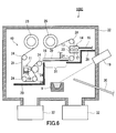
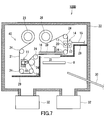
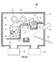
L'invention porte sur un dispositif de production de couche mince (100A) doté d'une cuve à vide (22), d'une source de dépôt (9) (source d'évaporation), d'un système de transport (40) et d'un dispositif d'enduction (11). La source de dépôt (9) est utilisée pour former une couche mince sur une première surface principale d'un substrat (21) dans une zone de dépôt (31) dans la cuve à vide (22). Le système de transport (40) est responsable du transport du substrat (21) d'un rouleau de déroulage (23) (position initiale) vers un rouleau d'enroulage (26) (position de récupération) le long d'un trajet de transport conçu de façon à ce que le substrat (21) passe dans la région de dépôt (31). Lors de la formation de la couche mince, le dispositif d'enduction (11) applique sur une seconde surface principale du substrat (21) une matière de refroidissement de substrat (10) qui peut être amenée à s'évaporer par l'application de chaleur au substrat (21).
Priority Applications (2)
| Application Number | Priority Date | Filing Date | Title |
|---|---|---|---|
| CN2012800091601A CN103392025A (zh) | 2011-03-11 | 2012-01-23 | 薄膜的制造方法和制造装置 |
| JP2012523161A JP5058396B1 (ja) | 2011-03-11 | 2012-01-23 | 薄膜の製造方法及び製造装置 |
Applications Claiming Priority (2)
| Application Number | Priority Date | Filing Date | Title |
|---|---|---|---|
| JP2011054719 | 2011-03-11 | ||
| JP2011-054719 | 2011-03-11 |
Publications (1)
| Publication Number | Publication Date |
|---|---|
| WO2012124246A1 true WO2012124246A1 (fr) | 2012-09-20 |
Family
ID=46830343
Family Applications (1)
| Application Number | Title | Priority Date | Filing Date |
|---|---|---|---|
| PCT/JP2012/000400 WO2012124246A1 (fr) | 2011-03-11 | 2012-01-23 | Procédé de production de couche mince et dispositif de production de couche mince |
Country Status (3)
| Country | Link |
|---|---|
| JP (1) | JP5058396B1 (fr) |
| CN (1) | CN103392025A (fr) |
| WO (1) | WO2012124246A1 (fr) |
Cited By (4)
| Publication number | Priority date | Publication date | Assignee | Title |
|---|---|---|---|---|
| JP2016219186A (ja) * | 2015-05-18 | 2016-12-22 | 株式会社アルバック | 正極活物質膜、および、成膜方法 |
| WO2019024326A1 (fr) * | 2017-07-31 | 2019-02-07 | 武汉华星光电半导体显示技术有限公司 | Appareil d'évaporation |
| JP2020158867A (ja) * | 2019-03-28 | 2020-10-01 | 芝浦メカトロニクス株式会社 | 成膜装置 |
| CN114231909A (zh) * | 2016-04-28 | 2022-03-25 | 佳能特机株式会社 | 真空蒸镀装置以及蒸发源的冷却方法 |
Families Citing this family (3)
| Publication number | Priority date | Publication date | Assignee | Title |
|---|---|---|---|---|
| CN108220890B (zh) * | 2016-12-15 | 2020-02-14 | 中国航空工业集团公司济南特种结构研究所 | 一种复材表面电弧离子镀膜方法 |
| CN112606372A (zh) * | 2020-12-15 | 2021-04-06 | 广东正一包装股份有限公司 | 一种高阻隔镀铝聚乙烯薄膜的制备方法 |
| CN113684464B (zh) * | 2021-08-27 | 2023-06-02 | 辽宁分子流科技有限公司 | 一种用于石墨烯复合薄膜制备的卷绕式设备 |
Citations (5)
| Publication number | Priority date | Publication date | Assignee | Title |
|---|---|---|---|---|
| JPH0348853U (fr) * | 1989-09-20 | 1991-05-10 | ||
| JP2006250909A (ja) * | 2005-03-14 | 2006-09-21 | Fuji Photo Film Co Ltd | 放射線像変換パネル |
| JP2009149963A (ja) * | 2007-12-22 | 2009-07-09 | Sumitomo Metal Mining Co Ltd | 真空成膜方法及び真空成膜装置 |
| WO2009104382A1 (fr) * | 2008-02-20 | 2009-08-27 | パナソニック株式会社 | Appareil de formation de film mince et procédé de formation de film mince |
| JP2010080855A (ja) * | 2008-09-29 | 2010-04-08 | Nikon Corp | 露光装置、露光方法及びデバイスの製造方法 |
Family Cites Families (1)
| Publication number | Priority date | Publication date | Assignee | Title |
|---|---|---|---|---|
| WO2007114314A1 (fr) * | 2006-03-30 | 2007-10-11 | Kabushiki Kaisha Mikuni Kogyo | Procede pour la formation d'une minuscule bosse metallique |
-
2012
- 2012-01-23 WO PCT/JP2012/000400 patent/WO2012124246A1/fr active Application Filing
- 2012-01-23 JP JP2012523161A patent/JP5058396B1/ja not_active Expired - Fee Related
- 2012-01-23 CN CN2012800091601A patent/CN103392025A/zh active Pending
Patent Citations (5)
| Publication number | Priority date | Publication date | Assignee | Title |
|---|---|---|---|---|
| JPH0348853U (fr) * | 1989-09-20 | 1991-05-10 | ||
| JP2006250909A (ja) * | 2005-03-14 | 2006-09-21 | Fuji Photo Film Co Ltd | 放射線像変換パネル |
| JP2009149963A (ja) * | 2007-12-22 | 2009-07-09 | Sumitomo Metal Mining Co Ltd | 真空成膜方法及び真空成膜装置 |
| WO2009104382A1 (fr) * | 2008-02-20 | 2009-08-27 | パナソニック株式会社 | Appareil de formation de film mince et procédé de formation de film mince |
| JP2010080855A (ja) * | 2008-09-29 | 2010-04-08 | Nikon Corp | 露光装置、露光方法及びデバイスの製造方法 |
Cited By (6)
| Publication number | Priority date | Publication date | Assignee | Title |
|---|---|---|---|---|
| JP2016219186A (ja) * | 2015-05-18 | 2016-12-22 | 株式会社アルバック | 正極活物質膜、および、成膜方法 |
| CN114231909A (zh) * | 2016-04-28 | 2022-03-25 | 佳能特机株式会社 | 真空蒸镀装置以及蒸发源的冷却方法 |
| CN114231909B (zh) * | 2016-04-28 | 2023-12-01 | 佳能特机株式会社 | 真空蒸镀装置以及蒸发源的冷却方法 |
| WO2019024326A1 (fr) * | 2017-07-31 | 2019-02-07 | 武汉华星光电半导体显示技术有限公司 | Appareil d'évaporation |
| JP2020158867A (ja) * | 2019-03-28 | 2020-10-01 | 芝浦メカトロニクス株式会社 | 成膜装置 |
| JP7319799B2 (ja) | 2019-03-28 | 2023-08-02 | 芝浦メカトロニクス株式会社 | 成膜装置 |
Also Published As
| Publication number | Publication date |
|---|---|
| JPWO2012124246A1 (ja) | 2014-07-17 |
| CN103392025A (zh) | 2013-11-13 |
| JP5058396B1 (ja) | 2012-10-24 |
Similar Documents
| Publication | Publication Date | Title |
|---|---|---|
| JP5058396B1 (ja) | 薄膜の製造方法及び製造装置 | |
| JP6724967B2 (ja) | プラズマを使った前処理装置を有した蒸着装置 | |
| US8697582B2 (en) | Substrate conveying roller, thin film manufacturing device, and thin film manufacturing method | |
| CN101889103B (zh) | 薄膜形成装置和薄膜形成方法 | |
| US8877291B2 (en) | Method of manufacturing thin film which suppresses unnecessary scattering and deposition of a source material | |
| JP5807216B2 (ja) | 薄膜の製造方法 | |
| JP6513221B2 (ja) | 方法及びコーティング設備 | |
| TWI526564B (zh) | Film forming apparatus and film forming method | |
| JPWO2018193993A1 (ja) | 成膜装置及び成膜方法 | |
| JP2012197477A (ja) | 薄膜製造方法および装置 | |
| JP4613048B2 (ja) | 圧力勾配型イオンプレーティング式成膜装置 | |
| JP2013008602A (ja) | リチウム二次電池用負極の製造装置および製造方法 | |
| JP2008291309A (ja) | 真空成膜装置 | |
| JP5050650B2 (ja) | 真空成膜方法 | |
| JP2012144783A (ja) | 薄膜製造装置及び薄膜製造方法 | |
| TW200304498A (en) | Method and apparatus for manufacturing thin film | |
| JP2012172261A (ja) | 成膜装置 | |
| WO2024022578A1 (fr) | Appareil de traitement pour traiter un substrat flexible et procédés associés | |
| WO1987005637A1 (fr) | Dispositif de plaquage ionique continu pour un film a defilement rapide | |
| JP2023502640A (ja) | スパッタ堆積 | |
| JP2004018895A (ja) | 薄膜製造装置、薄膜の製造方法および薄膜蒸着シートの製造方法 | |
| JP2012172260A (ja) | 成膜装置 | |
| JP2015209577A (ja) | 成膜装置および成膜方法 | |
| JPS6357767A (ja) | 高速移動フイルムの連続的シ−トプラズマ・イオンプレ−テイング装置 |
Legal Events
| Date | Code | Title | Description |
|---|---|---|---|
| ENP | Entry into the national phase |
Ref document number: 2012523161 Country of ref document: JP Kind code of ref document: A |
|
| 121 | Ep: the epo has been informed by wipo that ep was designated in this application |
Ref document number: 12757495 Country of ref document: EP Kind code of ref document: A1 |
|
| NENP | Non-entry into the national phase |
Ref country code: DE |
|
| 122 | Ep: pct application non-entry in european phase |
Ref document number: 12757495 Country of ref document: EP Kind code of ref document: A1 |