WO2012124246A1 - Thin-film production method and production device - Google Patents
Thin-film production method and production device Download PDFInfo
- Publication number
- WO2012124246A1 WO2012124246A1 PCT/JP2012/000400 JP2012000400W WO2012124246A1 WO 2012124246 A1 WO2012124246 A1 WO 2012124246A1 JP 2012000400 W JP2012000400 W JP 2012000400W WO 2012124246 A1 WO2012124246 A1 WO 2012124246A1
- Authority
- WO
- WIPO (PCT)
- Prior art keywords
- substrate
- thin film
- cooling material
- main surface
- formation region
- Prior art date
Links
Images


Classifications
-
- H—ELECTRICITY
- H01—ELECTRIC ELEMENTS
- H01M—PROCESSES OR MEANS, e.g. BATTERIES, FOR THE DIRECT CONVERSION OF CHEMICAL ENERGY INTO ELECTRICAL ENERGY
- H01M4/00—Electrodes
- H01M4/02—Electrodes composed of, or comprising, active material
- H01M4/04—Processes of manufacture in general
- H01M4/0402—Methods of deposition of the material
- H01M4/0421—Methods of deposition of the material involving vapour deposition
- H01M4/0423—Physical vapour deposition
- H01M4/0426—Sputtering
-
- C—CHEMISTRY; METALLURGY
- C23—COATING METALLIC MATERIAL; COATING MATERIAL WITH METALLIC MATERIAL; CHEMICAL SURFACE TREATMENT; DIFFUSION TREATMENT OF METALLIC MATERIAL; COATING BY VACUUM EVAPORATION, BY SPUTTERING, BY ION IMPLANTATION OR BY CHEMICAL VAPOUR DEPOSITION, IN GENERAL; INHIBITING CORROSION OF METALLIC MATERIAL OR INCRUSTATION IN GENERAL
- C23C—COATING METALLIC MATERIAL; COATING MATERIAL WITH METALLIC MATERIAL; SURFACE TREATMENT OF METALLIC MATERIAL BY DIFFUSION INTO THE SURFACE, BY CHEMICAL CONVERSION OR SUBSTITUTION; COATING BY VACUUM EVAPORATION, BY SPUTTERING, BY ION IMPLANTATION OR BY CHEMICAL VAPOUR DEPOSITION, IN GENERAL
- C23C14/00—Coating by vacuum evaporation, by sputtering or by ion implantation of the coating forming material
- C23C14/22—Coating by vacuum evaporation, by sputtering or by ion implantation of the coating forming material characterised by the process of coating
- C23C14/24—Vacuum evaporation
-
- C—CHEMISTRY; METALLURGY
- C23—COATING METALLIC MATERIAL; COATING MATERIAL WITH METALLIC MATERIAL; CHEMICAL SURFACE TREATMENT; DIFFUSION TREATMENT OF METALLIC MATERIAL; COATING BY VACUUM EVAPORATION, BY SPUTTERING, BY ION IMPLANTATION OR BY CHEMICAL VAPOUR DEPOSITION, IN GENERAL; INHIBITING CORROSION OF METALLIC MATERIAL OR INCRUSTATION IN GENERAL
- C23C—COATING METALLIC MATERIAL; COATING MATERIAL WITH METALLIC MATERIAL; SURFACE TREATMENT OF METALLIC MATERIAL BY DIFFUSION INTO THE SURFACE, BY CHEMICAL CONVERSION OR SUBSTITUTION; COATING BY VACUUM EVAPORATION, BY SPUTTERING, BY ION IMPLANTATION OR BY CHEMICAL VAPOUR DEPOSITION, IN GENERAL
- C23C14/00—Coating by vacuum evaporation, by sputtering or by ion implantation of the coating forming material
- C23C14/22—Coating by vacuum evaporation, by sputtering or by ion implantation of the coating forming material characterised by the process of coating
- C23C14/54—Controlling or regulating the coating process
- C23C14/541—Heating or cooling of the substrates
-
- C—CHEMISTRY; METALLURGY
- C23—COATING METALLIC MATERIAL; COATING MATERIAL WITH METALLIC MATERIAL; CHEMICAL SURFACE TREATMENT; DIFFUSION TREATMENT OF METALLIC MATERIAL; COATING BY VACUUM EVAPORATION, BY SPUTTERING, BY ION IMPLANTATION OR BY CHEMICAL VAPOUR DEPOSITION, IN GENERAL; INHIBITING CORROSION OF METALLIC MATERIAL OR INCRUSTATION IN GENERAL
- C23C—COATING METALLIC MATERIAL; COATING MATERIAL WITH METALLIC MATERIAL; SURFACE TREATMENT OF METALLIC MATERIAL BY DIFFUSION INTO THE SURFACE, BY CHEMICAL CONVERSION OR SUBSTITUTION; COATING BY VACUUM EVAPORATION, BY SPUTTERING, BY ION IMPLANTATION OR BY CHEMICAL VAPOUR DEPOSITION, IN GENERAL
- C23C14/00—Coating by vacuum evaporation, by sputtering or by ion implantation of the coating forming material
- C23C14/22—Coating by vacuum evaporation, by sputtering or by ion implantation of the coating forming material characterised by the process of coating
- C23C14/56—Apparatus specially adapted for continuous coating; Arrangements for maintaining the vacuum, e.g. vacuum locks
- C23C14/562—Apparatus specially adapted for continuous coating; Arrangements for maintaining the vacuum, e.g. vacuum locks for coating elongated substrates
-
- H—ELECTRICITY
- H01—ELECTRIC ELEMENTS
- H01M—PROCESSES OR MEANS, e.g. BATTERIES, FOR THE DIRECT CONVERSION OF CHEMICAL ENERGY INTO ELECTRICAL ENERGY
- H01M4/00—Electrodes
- H01M4/02—Electrodes composed of, or comprising, active material
- H01M4/13—Electrodes for accumulators with non-aqueous electrolyte, e.g. for lithium-accumulators; Processes of manufacture thereof
- H01M4/139—Processes of manufacture
- H01M4/1395—Processes of manufacture of electrodes based on metals, Si or alloys
-
- Y—GENERAL TAGGING OF NEW TECHNOLOGICAL DEVELOPMENTS; GENERAL TAGGING OF CROSS-SECTIONAL TECHNOLOGIES SPANNING OVER SEVERAL SECTIONS OF THE IPC; TECHNICAL SUBJECTS COVERED BY FORMER USPC CROSS-REFERENCE ART COLLECTIONS [XRACs] AND DIGESTS
- Y02—TECHNOLOGIES OR APPLICATIONS FOR MITIGATION OR ADAPTATION AGAINST CLIMATE CHANGE
- Y02E—REDUCTION OF GREENHOUSE GAS [GHG] EMISSIONS, RELATED TO ENERGY GENERATION, TRANSMISSION OR DISTRIBUTION
- Y02E60/00—Enabling technologies; Technologies with a potential or indirect contribution to GHG emissions mitigation
- Y02E60/10—Energy storage using batteries
Definitions
- the present invention relates to a thin film manufacturing method and manufacturing apparatus.
- Thin film technology is widely deployed to improve the performance and miniaturization of devices.
- the thinning of devices is not only a direct merit for users, but also plays an important role in environmental aspects such as protecting earth resources and reducing power consumption.
- the winding-type thin film manufacturing method is a method in which a long substrate is unwound from a winding roller, a thin film is formed on the substrate while being transported along the transport path, and then the substrate is wound on the winding roller. .
- a thin film can be formed with high productivity by combining a film formation source having a high deposition rate such as a vacuum evaporation source using an electron beam with a winding thin film manufacturing method. Further, when a thin film is continuously formed on each of the plate-like discrete substrates, a large number of stacked substrates are sequentially sent out from the delivery stocker to the film formation region. After film formation, the substrates are sequentially stored in a collection stocker.
- a film formation source having a high deposition rate such as a vacuum evaporation source using an electron beam with a winding thin film manufacturing method.
- the substrate can be cooled by a cylindrical can. Specifically, a thin film is formed on a substrate running along a cylindrical can. If the thermal contact between the substrate and the cylindrical can is ensured, heat can be released to the cylindrical can having a large heat capacity, so that an increase in the temperature of the substrate can be prevented. Further, the temperature of the substrate can be maintained at a specific cooling temperature. The cooling of the substrate by the cylindrical can is also effective in the transfer path other than the film formation region. In order to improve the adhesion between the cylindrical can and the substrate, the attachment of the substrate to the cylindrical can may be strengthened using an electron beam.
- Patent Document 1 discloses that in an apparatus for forming a thin film on a web that is a substrate, a gas is introduced into a region between the web and a support means. According to this method, since heat conduction between the web and the support means can be ensured, an increase in the temperature of the web can be suppressed.
- Patent Document 2 discloses a method of cooling a cylindrical can by making the inside of a cylindrical cooling part of the cylindrical can an independent decompression system and evaporating the refrigerant along the inner wall surface of the cylindrical cooling part.
- Patent Document 3 discloses a belt cooling method when a belt is used for transporting and cooling a substrate material. According to this method, in order to further cool the cooling belt, a cooling mechanism using a double or more cooling belt or a liquid medium is provided inside. Thereby, since the cooling efficiency can be increased, the characteristics of the magnetic tape including the electromagnetic conversion characteristics can be improved, and at the same time, the productivity can be greatly improved.
- substrate can be made to contact a support block. In order to improve heat conduction between the support block and the substrate, it is effective to introduce a gas between the substrate and the support block.
- JP-A-1-152262 Japanese Patent Publication No. 3-59987 JP-A-6-145982
- An object of the present invention is to solve the above-described conventional problems, and to provide a thin film manufacturing method and a manufacturing apparatus capable of achieving a high substrate cooling capability while suppressing deterioration of the degree of vacuum.
- the present invention Forming a thin film on the first main surface of the substrate in a vacuum; Prior to the thin film formation step, a step of applying a substrate cooling material that can be evaporated by heat applied to the substrate when forming the thin film to the second main surface of the substrate; A method for producing a thin film is provided.
- the present invention provides: A vacuum chamber; A film-forming source disposed in the vacuum chamber and forming a thin film on the first main surface of the substrate in a film-forming region in the vacuum chamber; A transport system that is disposed in the vacuum chamber and transports the substrate from a delivery position to a recovery position along a transport path set so that the substrate passes through the film formation region; A coater for applying to the second main surface of the substrate a substrate cooling material that can be evaporated by heat applied to the substrate when forming the thin film; An apparatus for manufacturing a thin film is provided.
- the substrate can be cooled by the heat of vaporization of the substrate cooling material applied to the second main surface. Since the vaporization heat of the substrate cooling material is used, more heat can be taken from the substrate with a small amount of the substrate cooling material than in the case of direct cooling with gas. Therefore, according to the present invention, a high cooling capacity can be achieved while suppressing the deterioration of the degree of vacuum.
- the present invention does not exclude the use of conventional gas cooling. It is also possible to use the present invention in combination with gas cooling.
- main surface means a surface having the widest area.
- first main surface corresponds to the front surface of the substrate
- second main surface corresponds to the back surface of the substrate.
- FIG. 1 Schematic of a thin film manufacturing apparatus according to an embodiment of the present invention. Partial enlarged view of FIG. The figure which shows the method of providing a substrate cooling material to the linear part of a substrate Figure showing another example of evaporation source
- Schematic of thin film manufacturing apparatus according to Modification 1 Schematic of thin film manufacturing apparatus according to Modification 2
- Schematic of thin film manufacturing apparatus according to Modification 3 Schematic of thin film manufacturing apparatus according to Modification 4
- Partial enlarged view of FIG. Schematic of thin film manufacturing apparatus according to Modification 5
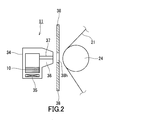
- the thin film manufacturing apparatus 100A includes a vacuum chamber 22, a transport system 40, an evaporation source 9 (film formation source), and a coater 11 (coater).
- the evaporation source 9, the transport system 40 and the coater 11 are disposed inside the vacuum chamber 22.
- the substrate cooling material 10 is applied to the second main surface of the substrate 21 by the coater 11.
- the substrate cooling material 10 is evaporated by heat applied to the substrate 21 when a thin film is formed on the substrate 21.
- the substrate 21 is cooled by the heat of vaporization of the substrate cooling material 10. Thereby, it is possible to prevent the substrate 21 from being damaged by heat.
- the vacuum chamber 22 is composed of a pressure-resistant container.
- a vacuum pump 32 is connected to the vacuum chamber 22.
- a shielding plate 29, an electron gun 19, and a source gas introduction pipe 30 are provided inside the vacuum chamber 22.
- the inside of the vacuum chamber 22 is partitioned by a shielding plate 29 into a region where the evaporation source 9 is disposed and a region where the transport system 40 is disposed.
- the shielding plate 29 has an opening for forming the film formation region 31 on the transport path of the substrate 21. When the substrate 21 passes through the film formation region 31, raw material particles flying from the evaporation source 9 are deposited on the substrate 21.
- the transport system 40 forms a transport path for the substrate 21 in the vacuum chamber 22 and plays a role of transporting the substrate 21 from the delivery position to the collection position along the transport path.
- the transport path is set so that the substrate 21 passes through the film formation region 31. Specifically, the transport path is set so that the substrate 21 travels linearly in the film formation region 31. In the film formation region 31, the raw material particles from the evaporation source 9 enter the substrate 21 substantially perpendicularly.
- the transport system 40 is constituted by an unwind roller 23, a transport roller 24, and a take-up roller 26.
- a substrate 21 before film formation is prepared on the unwinding roller 23.
- the unwinding roller 23 supplies the substrate 21 toward the transport roller 24 disposed closest to the unwinding roller 23.
- the transport roller 24 disposed upstream in the transport direction of the substrate 21 guides the substrate 21 supplied from the unwinding roller 23 to the film formation region 31.
- the transport roller 24 disposed downstream in the transport direction guides the substrate 21 to the take-up roller 26.
- the take-up roller 26 is driven by a driving means (not shown) such as a motor, and takes up and stores the substrate 21 after film formation.
- the unwinding roller 23 and the take-up roller 26 constitute a sending position and a collecting position for the substrate 21, respectively.
- the evaporation source 9 is used to form a thin film on the first main surface of the substrate 21 in the film formation region 31.
- the evaporation source 9 includes a crucible that holds a thin film material, and is provided below the film formation region 31.
- the raw material held in the evaporation source 9 is heated and evaporated.
- the raw material vapor moves upward and adheres to the substrate 21 in the film formation region 31. As a result, a thin film is formed on the substrate 21.
- a raw material supply machine for adding a raw material to the evaporation source 9 without purging the vacuum may be provided inside the vacuum chamber 22.
- the form of the raw material to be supplied is not particularly limited.
- a raw material melt generated by melting a rod-shaped raw material can be supplied to the evaporation source 9 in the form of droplets. This method is preferable because the temperature change of the melt held in the evaporation source 9 can be suppressed and the evaporation rate of the raw material hardly fluctuates.
- An electron beam can be used to melt the rod-shaped raw material.
- the thin-film manufacturing apparatus 100A can be simplified, so that a reduction in cost can be expected.
- Both the straight gun and the deflection gun can be used as the electron gun 19.
- a straight gun having a high output and a wide scanning range of the electron beam.
- it is effective to bend the trajectory of the electron beam about several degrees from the viewpoint of preventing contamination inside the barrel of the electron gun 19.
- a rectangular crucible having an opening width wider than the film forming width can be used as the evaporation source 9 in continuous vacuum deposition represented by a winding type. Such a crucible is effective from the viewpoint of ensuring film thickness uniformity in the width direction of the substrate 21.
- the irradiation position of the electron beam for melting the rod-shaped raw material and the dropping position of the molten raw material on the evaporation source 9 are outside the scanning range of the electron beam for evaporating the melt held in the evaporation source 9. Can be set. If it does in this way, the temperature change of the melt by adding a raw material and the vibration of the surface of a melt can be controlled. That is, the influence on the film forming conditions can be reduced. Control of the irradiation position of the electron beam is achieved by using an electron beam scanning circuit provided in the electron gun system and finely controlling a coil current for generating a magnetic field.
- the source gas introduction pipe 30 has one end directed to the space inside the vacuum chamber 22 and the other end extending to the outside of the vacuum chamber 22.
- One end of the source gas introduction pipe 30 is directed, for example, to a space between the evaporation source 9 and the film formation region 31.
- the other end of the source gas introduction pipe 30 is connected to a source gas supply source such as a gas cylinder or a gas generator outside the vacuum chamber 22. If the source gas introduction pipe 30 is used, a gas such as oxygen or nitrogen can be mixed with the source material evaporated from the evaporation source 9. As a result, a thin film containing a raw material oxide, nitride or oxynitride as a main component evaporated from the evaporation source 9 is formed on the substrate 21.
- the vacuum pump 32 is connected to the vacuum chamber 22.
- various vacuum pumps such as a rotary pump, an oil diffusion pump, a cryopump, and a turbo molecular pump can be used.
- the coater 11 is used to apply the substrate cooling material 10 to the second main surface of the substrate 21, that is, the surface opposite to the surface on which the thin film is to be formed.
- the position of the coater 11 is such that the substrate cooling material 10 is applied to the second main surface of the substrate 21 on the transport path between the unwinding roller 23 (delivery position) and the film formation region 31. Is set. If the substrate cooling material 10 is applied to the substrate 21 immediately before the film formation, it is possible to prevent the substrate cooling material 10 from detaching from the substrate 21 before reaching the film formation region 31 as much as possible.
- the coater 11 is configured to deposit the substrate cooling material 10 on the second main surface of the substrate 21. According to the vapor deposition method, the substrate cooling material 10 can be applied to the substrate 21 with a uniform and minimum necessary thickness relatively easily.
- the coater 11 includes a container 34, a heater 35, and a nozzle 36.
- the container 34 holds the substrate cooling material 10.
- the heater 35 heats the substrate cooling material 10 held in the container 34.
- the nozzle 36 is provided with a discharge port 37 (slit) extending from the inside of the container 34 toward the second main surface of the substrate 21.
- the width (inner diameter) of the discharge port 37 is, for example, 0.05 to 0.2 mm.
- the coater 11 may be configured so that the substrate cooling material 10 can be supplied to the container 34 from the outside of the vacuum chamber 22 without purging the vacuum.
- the configuration of the coater 11 is not limited.
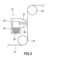
- the coater 11 may have a plurality of discharge ports 37 arranged at regular intervals along the transport direction of the substrate 21.
- the interval between the discharge ports 37 adjacent to each other is, for example, 2 to 10 mm.
- a metal sintered body having a plurality of pores and space passages may be provided in the coater 11.
- the coater 11 is appropriately separated from the substrate 21.
- the distance between the coater 11 and the substrate 21 is, for example, 2 to 20 mm.
- a heat shielding material 38 may be provided between the coater 11 and the substrate 21.
- the heat shield 38 has an opening 38h. The opening 38 h faces the discharge port 37 of the coater 11. The vapor of the substrate cooling material 10 advances from the coater 11 to the substrate 21 through the opening 38h.
- the substrate cooling material 10 is sprayed on the substrate 21 in the form of vapor. Since the temperature of the substrate 21 increases when the substrate cooling material 10 is applied, it is desirable to cool the substrate 21 before reaching the film formation region 31. According to the present embodiment, after the substrate cooling material 10 is applied, the substrate 21 contacts the transport roller 24 before reaching the film formation region 31. The substrate 21 is cooled by the transport roller 24. Further, in the transport path between the unwinding roller 23 and the film forming region 31, the substrate 21 has a portion supported by the transport roller 24. The substrate cooling material 10 is applied to the supported part. In this way, the temperature rise of the substrate 21 based on the provision of the substrate cooling material 10 to the substrate 21 can be suppressed.
- the second main surface of the substrate 21 is not in contact with the transfer roller 24, and only the first main surface of the substrate 21 is transferred. That is, the conveyance system 40 is configured to be supported by the roller 24. In this way, the substrate 21 can be cooled by the transport roller 24 while preventing the substrate cooling material 10 from adhering to the transport roller 24. Further, the cooling may be performed by radiation cooling.
- the coater 11 may be configured to spray or drop the liquid substrate cooling material 10 onto the substrate 21.
- the coater 11 has a rotating body impregnated with the substrate cooling material 10, and the substrate cooling material 10 can be applied to the substrate 21 by bringing the substrate 21 into contact with the rotating body.
- the method for applying the substrate cooling material 10 is not limited as long as the degree of vacuum is not significantly deteriorated.
- the posture of the substrate 21 when the substrate cooling material 10 is applied is not particularly limited.
- the substrate cooling material 10 can be applied to the substrate 21 stretched linearly.
- the substrate cooling material 10 can be applied to the substrate 21 that is traveling linearly between the transport rollers 24.
- the substrate 21 is prepared on the unwinding roller 23.
- a long and strip-shaped substrate can be used.
- substrate 21 is not specifically limited, Metal foil, a polymer film, these composite bodies, etc. can be used.
- the metal foil include aluminum foil, copper foil, nickel foil, titanium foil, and stainless steel foil.
- the polymer film include films made of resins such as polyethylene terephthalate, polyethylene naphthalate, polyamide, and polyimide.
- the dimensions of the substrate 21 are not particularly limited.
- the substrate 21 has, for example, a width of 50 to 1000 mm and a thickness of 3 to 150 ⁇ m. If the width of the substrate 21 is too wide or too narrow, there may be a problem in terms of productivity. If the substrate 21 is too thin, the heat capacity of the substrate 21 is extremely small, and thermal damage is likely to occur. However, these problems do not hinder the implementation of the present invention.
- a metal foil typically a copper foil (including a copper alloy foil) is used for the substrate 21 as a current collector.
- the surface of the copper foil may be roughened.
- Such copper foil is available from, for example, Furukawa Circuit Foil.
- the copper foil may be rolled.
- silicon is prepared in the evaporation source 9 as an active material of the lithium ion secondary battery.
- the melting point of silicon is as high as about 1410 ° C. Therefore, a relatively large heat load is applied to the substrate 21 during film formation. A large heat load reduces the strength (tensile strength) of the substrate 21.
- the method described in the present embodiment can be suitably used for manufacturing the electrode plate of the lithium ion secondary battery.
- the vacuum pump 32 is moved to exhaust the inside of the vacuum chamber 22.
- the inside of the vacuum chamber 22 is maintained at a pressure suitable for forming a thin film, for example, 1.0 ⁇ 10 ⁇ 2 to 1.0 ⁇ 10 ⁇ 4 Pa.
- the raw material of the thin film held in the evaporation source 9 is heated.
- the raw material is in a liquid phase in which a part thereof is being evaporated by heating with an electron beam.
- the acceleration voltage of the electron beam is about ⁇ 8 to ⁇ 30 kW, and the output of the electron beam is about 5 to 280 kW.
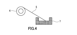
- a heating method other than the electron beam For example, when manufacturing a capacitor electrode plate, an aluminum oxide thin film is formed on the substrate 21. As shown in FIG. 4, aluminum can be dissolved and evaporated by resistance heating while supplying aluminum (aluminum wire 5) as a thin film constituent material from the raw material supplier 6 to the boat 7. When oxygen gas is supplied from the source gas introduction pipe 30 toward the film formation region 31, aluminum oxide is deposited on the substrate 21. A plurality of boats 7 may be arranged in the width direction of the substrate 21. The same applies to the evaporation source 9.
- the substrate 21 is transferred from the unwinding roller 23 to the take-up roller 26 along the transfer path (transfer process).
- a thin film is formed on the first main surface of the substrate 21 in the film forming region 31 set on the transport path (thin film forming step).
- an operation for supplying the substrate 21 from the unwinding roller 23 to the film forming region 31 and an operation for collecting the substrate 21 from the film forming region 31 to the take-up roller 26 are performed in synchronization. That is, the thin film manufacturing apparatus 100 ⁇ / b> A is a so-called winding type thin film manufacturing apparatus that forms a thin film on the substrate 21 being conveyed from the unwinding roller 23 to the winding roller 26. According to the roll-up type thin film manufacturing apparatus, high productivity can be achieved because continuous film formation for a long time is possible.
- the substrate 21 may be a discrete substrate.
- a large number of stacked substrates are sequentially sent from a delivery stocker to a film formation region. After film formation, the substrates are sequentially stored in a collection stocker.
- the substrate cooling material 10 can be applied to the discrete substrate on the transport path from the delivery stocker (delivery position) to the film formation region.
- the conveyance speed of the substrate 21 varies depending on the type of thin film and film forming conditions, and is, for example, 0.1 to 500 m / min.
- the average film formation rate is not particularly limited, and is, for example, 20 to 800 nm / second.
- a tension having an appropriate strength is applied to the substrate 21 being transported in the longitudinal direction of the substrate 21. The strength of the tension is appropriately adjusted depending on conditions such as the material of the substrate 21, the thickness of the substrate 21, and the film forming speed.
- a metal mask having an opening length of 50 to 400 mm in the width direction of the substrate 21 is disposed in the film formation region 31 so that a thin film having a certain width (for example, 100 to 600 mm) is formed on the substrate 21. (Not shown).
- the distance from the substrate 21 to the metal mask is, for example, 1 to 8 mm.
- the coater 11 Prior to the thin film forming process, the coater 11 is used to apply the substrate cooling material 19 to the second main surface of the substrate 21 on the transport path between the unwinding roller 23 and the film forming region 31 (applying process). .
- the substrate cooling material 10 is discharged from the discharge port 37 of the coater 11 in the form of vapor, reaches the second main surface of the substrate 21, and is liquefied or solidified into a thin film on the second main surface.
- the substrate cooling material 10 maintains a liquid phase or a solid phase state on the second main surface before the thin film forming step. Therefore, the substrate 21 can be cooled by the heat of vaporization (latent heat) of the substrate cooling material 10. This point is greatly different from conventional gas cooling.
- a material containing at least one selected from the group consisting of hydrocarbons, oils and higher alcohols can be used. These materials are suitable because they hardly remain as residues on the substrate 21.
- the hydrocarbon include alkanes such as decane, undecane, dodecane, and tridecane.
- the oil include fluorine oils such as Fomblin (registered trademark of Solvay Solexis) Y03, Fomblin Y06, and the like.
- the higher alcohol include those having 8 to 12 carbon atoms, such as octanol.
- a polymer material having a relatively low melting point such as low-density polyethylene can be used.
- a liquid or solid material can be used for the substrate cooling material 10 in a vacuum environment when forming a thin film.
- the composition of the substrate cooling material 10 includes the material of the substrate 21, the thickness of the substrate 21, the temperature reached by the substrate 21, the constituent material of the thin film, the deposition rate, the intensity of radiant heat, the required degree of cooling, the degree of vacuum, etc. Appropriately determined in consideration of various conditions.
- octanol can be used as the substrate cooling material 10.
- a discharge port 37 provided with a porous metal sintered body can be used.
- fluorine oil can be used as the substrate cooling material 10.
- one having a plurality of discharge ports 37 can be used.
- the thickness of the substrate cooling material 10 on the second main surface of the substrate 21 is not particularly limited.
- the substrate cooling material 10 has a thickness of 5 to 100 nm.
- the substrate cooling material 10 applied to the substrate 21 is transported together with the substrate 21 and reaches the film formation region 31.
- a thin film is formed on the first main surface of the substrate 21 while receiving heat from the raw material particles flying from the evaporation source 9 and radiation heat from the evaporation source 9.
- the substrate cooling material 10 takes heat from the substrate 21 and evaporates.
- the substrate 21 is heated by the formation of a thin film while being cooled by evaporation of the substrate cooling material 10. Therefore, the temperature rise of the substrate 21 can be suppressed.
- the entire amount of the substrate cooling material 10 may evaporate in the film formation region 31 or may remain slightly on the substrate 21. Even if a small amount of the substrate cooling material 10 remains on the substrate 21, the possibility of adversely affecting the quality of the thin film is low.
- a step of removing the substrate cooling material 10 from the substrate 21 may be performed as necessary.
- the substrate cooling material 10 can be removed from the substrate 21 by a method such as wiping, heating, and plasma irradiation described later.
- the substrate cooling material 10 remaining on the substrate 21 and the substrate cooling material 10 adhering to the members inside the vacuum chamber 22 can be detected by an evolved gas analysis (EGA) or other microchemical analysis.
- ESA evolved gas analysis
- the substrate 21 after film formation is analyzed by the generated gas analysis method, it can be checked whether the substrate cooling material 10 remains on the substrate 21.
- the substrate 21 is unwound from the unwinding roller 23 and then reaches the film formation region 31 via the transport roller 24.
- a thin film is formed on the first main surface of the substrate 21.
- the source gas may be supplied from the source gas introduction pipe 30 toward the film formation region 31.
- a thin film made of a compound of the raw material held in the evaporation source 9 and the raw material supplied from the raw material gas introduction pipe 30 can be formed.
- the substrate 21 is taken up by the take-up roller 26 via another transport roller 24.
- the step of applying the substrate cooling material 10 to the second main surface of the substrate 21 and the step of forming a thin film are performed on the moving substrate 21. That is, each process is performed while moving the substrate 21 slowly. Therefore, a thin film can be formed with high productivity.
- the substrate 21 can be moved intermittently little by little. That is, the substrate cooling material 10 may be applied on the substrate 21 that is temporarily stopped, or a thin film may be formed.
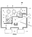
- FIG. 5 is a schematic view of a thin film manufacturing apparatus 100B provided with a sputtering source 8 as a film forming source.
- the sputter source 8 is disposed below the film formation region 31.
- the sputter source 8 can be used for manufacturing a transparent electrode, for example.
- a resin film such as a polyethylene terephthalate film can be used.
- an inert gas such as argon gas is introduced into the vacuum chamber 22, and the first target of the substrate 21 is formed by high-frequency sputtering using an ITO target that is a constituent material of the sputtering source 8.
- An ITO thin film is formed on the main surface.
- an ITO thin film having a thickness of 0.3 to 10 ⁇ m can be formed on a substrate 21 having a thickness of 10 to 150 ⁇ m.
- the average film formation rate by the sputtering method is generally slower than the average film formation rate by the vapor deposition method, for example, 0.5 to 5 nm / second.
- the conveyance speed of the substrate 21 is, for example, 0.05 to 1 m / min.
- FIG. 6 is a schematic diagram of a thin film manufacturing apparatus 100 ⁇ / b> C further including a plasma generator 14 and a heat receiving body 16 in addition to the configuration described with reference to FIG. 1. Only one of the plasma generator 14 and the heat receiving body 16 may be provided.
- the heat receiving body 16 faces the second main surface of the substrate 21 in the film formation region 31 and can receive heat from the substrate cooling material 10 evaporated from the second main surface of the substrate 21.
- the conveyance path is designed so that the substrate 21 travels linearly in the film formation region 31. Therefore, a member having a flat surface facing the substrate 21 can be suitably used as the heat receiving body 16. In this case, the distance between the heat receiving body 16 and the substrate 21 can be kept constant.
- the substrate cooling material 10 evaporates by heat applied to the substrate 21 in the film formation region 31 and takes heat of vaporization from the substrate 21.
- the evaporated substrate cooling material 10 stays for a while in the form of gas molecules between the substrate 21 and the heat receiving body 16.
- the gas molecules of the substrate cooling material 10 promote heat conduction between the substrate 21 and the heat receiving body 16. That is, the evaporated substrate cooling material 10 becomes a medium, and a high cooling effect can be obtained.
- One method for cooling the substrate in vacuum is to introduce a gas between the substrate and the support. According to this method, heat conduction between the substrate and the support is promoted by the gas.
- this modification both the effect of cooling the substrate 21 by the heat of vaporization of the substrate cooling material 10 and the effect of promoting the heat conduction between the substrate 21 and the heat receiving body 16 by the substrate cooling material 10 are obtained. It is done. Therefore, even if the load applied to the vacuum pump by gas cooling is approximately the same as the load applied to the vacuum pump 32 in this modification, this modification can exhibit a higher cooling effect than mere gas cooling.
- the heat receiving body 16 is preferably disposed near the substrate 21.
- the distance between the substrate 21 and the heat receiving body 16 is set to 0.1 to 3 mm, for example. When this interval is appropriately adjusted, the effect of promoting the heat conduction between the substrate 21 and the heat receiving body 16 by the evaporated substrate cooling material 10 is sufficiently prevented while preventing the heat receiving body 16 and the substrate 21 from contacting each other. Obtainable.
- the heat receiving body 16 also exhibits an effect of preventing the evaporated substrate cooling material 10 from being scattered inside the vacuum chamber 22. Therefore, the heat receiving body 16 preferably has a width wider than that of the substrate 21 in the width direction of the substrate 21.
- the heat receiving body 16 may be cooled by the cooler 39.
- the structure of the cooler 39 is not particularly limited. Examples of the cooler 39 include those using refrigerants such as water, antifreeze, and oil.
- the cooler 39 may be built in the heat receiving body 16 or may be only in contact with the heat receiving body 16.
- the heat receiving body 16 can be cooled by circulating the refrigerant cooled outside the vacuum chamber 22 to the cooler 39 using a refrigerator or the like.
- the material of the heat receiving body 16 is not particularly limited. A material such as metal, ceramic, or glass can be used as the material of the heat receiving body 16. When the heat receiving body 16 is made of a material that can easily maintain a low temperature and has a high emissivity, the effect of radiation cooling increases.
- the heat receiving body 16 may have a function of collecting the substrate cooling material 10.
- the lower part of the heat receiving body 16 faces the substrate 21, the lower part of the heat receiving body 16 may have an adsorption function.
- the heat receiving body 16 is composed of a simple metal block, the substrate cooling material 10 may adhere to the heat receiving body 16 without being exhausted and may eventually fall onto the substrate 21. In order to prevent this phenomenon, it is effective to provide holes and / or protrusions on the surface of the heat receiving body 16 or to provide a porous structure on the surface of the heat receiving body 16.
- part or all of the heat receiving body 16 may be made of an adsorbent that captures the substrate cooling material 10, typically a porous material. It is preferable that such an adsorbent is disposed in the film formation region 31 at a position facing the second main surface of the substrate 21 because the substrate cooling material 10 is unlikely to scatter in the vacuum chamber 22.
- the plasma generator 14 is provided on a conveyance path between the film formation region 31 and the take-up roller 26 (collection position). After film formation, the plasma generator 14 is used to decompose the substrate cooling material 10 remaining on the second main surface of the substrate 21.
- the plasma generator 14 includes a gas introduction tube 15, a discharge electrode 17, and a housing 20.
- the semi-sealed housing 20 is provided with two slits as entrances for the substrate 21.
- a conveyance path is set so that the substrate 21 passes through the inside of the housing 20.
- the gas introduction pipe 15 has one end connected to the housing 20 and the other end extending to the outside of the vacuum chamber 22.
- the other end of the gas introduction pipe 15 is connected to a gas supply source such as a gas cylinder or a gas generator outside the vacuum chamber 22.
- the discharge electrode 17 is provided inside the housing 20.
- the gas supplied to the housing 20 through the gas introduction tube 15 is excited by the discharge electrode 17, and plasma is generated inside the housing 20.
- the substrate cooling material 10 remaining on the substrate 21 is decomposed by the plasma generated around the substrate 21.
- the decomposition product of the substrate cooling material 10 is relatively easily separated from the substrate 21 and exhausted. Since the decomposition product has a smaller molecular weight than the substrate cooling material 10, it is exhausted as a gas with a high probability without adhering to the members inside the vacuum chamber 22.
- the composition of the process gas for generating plasma is not particularly limited.
- oxygen gas is used as a process gas for ashing organic substances.
- Oxygen gas is easy to handle.
- Oxygen plasma has a high ability to decompose organic substances, and can quickly decompose the substrate cooling material 10 into low molecular weight hydrocarbons, CO x , H 2 O, and the like.
- ozone gas, rare gas, nitrogen gas, halogen gas, hydrogen gas, chlorofluorocarbon gas and the like can be used. It is also possible to use a mixture of two or more gases, for example, a mixed gas of oxygen gas as a main component and a small amount of halogen gas.
- the “main component” means a component that is contained most in volume ratio.
- the flow rate of the process gas to be introduced into the housing 20 is not particularly limited, and is determined in consideration of the state of plasma discharge, the required degree of vacuum, and the like.
- the state of the plasma discharge also depends on the conductance of the housing 20 and the capacity of the exhaust pump 32. It should be noted that a sufficient degree of vacuum is required for the evaporation source 9 and the film formation region 31 in order to form a high-quality thin film.
- the flow rate of the process gas is controlled by a mass flow controller, and is, for example, 10 to 500 sccm (Standard Cubic Centimeter per Minute).
- the voltage to be applied to the discharge electrode 17 may be either direct current or alternating current.
- a high frequency voltage may be applied to the discharge electrode 17.
- the applied voltage is 500 to 1500 V, for example, although it depends on the pressure inside the casing 20 and the type of process gas.
- the supply power in the case of high frequency is, for example, 50 to 500 W (or 50 to 300 W).
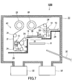
- FIG. 7 shows a combination of the first modification described with reference to FIG. 3 and the second modification described with reference to FIG. That is, the thin film manufacturing apparatus 100 ⁇ / b> D includes a sputtering source 8, a heat receiving body 16, and a plasma generator 14. As described above, the configurations described in the present specification can be appropriately combined as long as the cooling effect of the substrate 21 by the substrate cooling material 10 is obtained.
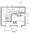
- FIG. 8 is a schematic diagram of a thin film manufacturing apparatus 100E further including a plasma generator 14 and a recovery mechanism 42 in addition to the configuration described with reference to FIG.
- the recovery mechanism 42 is provided at a position facing the second main surface of the substrate 21 staying in the film formation region 31. If the recovery mechanism 42 is used, the substrate cooling material 10 evaporated in the film formation region 31 can be efficiently recovered in the film formation region 31. Therefore, it is possible to prevent the substrate cooling material 10 from adversely affecting the quality of the thin film or scattering inside the vacuum chamber 22.
- the recovery mechanism 42 includes a gas introduction tube 15, a discharge electrode 17, an exhaust port 18, and a housing 43.
- the housing 43 opens toward the second main surface of the substrate 21, and prevents the substrate cooling material 10 evaporated from the second main surface of the substrate 21 from being scattered inside the vacuum chamber 22.
- the second main surface of the substrate 21 is covered with a housing 43.
- the exhaust port 18 is provided at a position facing the second main surface of the substrate 21 staying in the film formation region 31.
- a plurality of exhaust ports 18 are provided in a portion corresponding to the ceiling of the housing 43. The substrate cooling material 10 evaporated in the film forming region 31 is exhausted to the outside of the vacuum chamber 22 through the exhaust port 18.
- the position of the exhaust port 18 in the housing 43 is not particularly limited.
- the exhaust port 18 may not face the second main surface of the substrate 21.
- the substrate cooling material 10 is cooled through the exhaust port 18 before the substrate cooling material 10 leaks outside the housing 43 and diffuses into the vacuum chamber 22. The probability that the material 10 can be quickly exhausted to the outside of the vacuum chamber 22 is increased.
- an exhaust pipe 45 is connected to each exhaust port 18.
- the exhaust pipe 45 is connected to a vacuum pump 46 provided outside the vacuum chamber 22. That is, in addition to the vacuum pump 32 for exhausting the inside of the vacuum chamber 22, a vacuum pump 46 for exhausting the interior of the housing 43 through the exhaust port 18 and the exhaust pipe 45 is provided. According to such a structure, the substrate cooling material 10 can be recovered more efficiently.
- the dimension (inner diameter) of the exhaust port 18 is not particularly limited, and is, for example, 5 to 50 mm.
- the recovery mechanism 42 further includes a plasma generator 47.
- the plasma generator 47 includes the gas introduction tube 15 and the discharge electrode 17.
- the gas introduction pipe 15 has one end connected to the housing 43 and the other end extending to the outside of the vacuum chamber 22.
- the other end of the gas introduction pipe 15 is connected to a gas supply source such as a gas cylinder or a gas generator outside the vacuum chamber 22.
- the discharge electrode 17 is provided inside the housing 43. Specifically, the discharge electrode 17 is provided between the substrate 21 and the exhaust port 18.
- one end of the gas introduction pipe 15 opens toward the space between the substrate 21 and the exhaust port 18. According to such a positional relationship, plasma is generated in the space between the substrate 21 and the exhaust port 18.
- the substrate cooling material 10 evaporates in the film formation region 31 and is decomposed by plasma on the path from the substrate 21 to the exhaust port 18.
- the decomposition product of the substrate cooling material 10 is exhausted relatively easily.
- the housing 43 may have a wall portion in the width direction of the substrate 21.
- gas leakage can be reduced.
- FIG. 10 is a schematic view of a thin film manufacturing apparatus 100F further including a first plasma generator 14, a second plasma generator 54, and a cylindrical can 25 in addition to the configuration described with reference to FIG.
- the plasma generators 14 and 54 may be omitted.
- the thin film manufacturing apparatus 100F includes a transport system 50 having a cylindrical can 25 (can roller).
- the cylindrical can 25 is a roller-like member that can rotate at the same speed as the conveyance speed of the substrate 21, and is disposed in the film formation region 31. Specifically, a part of the outer peripheral surface of the cylindrical can 25 faces the film formation region 31. A part of the conveyance path by the conveyance system 50 is formed by a cylindrical can 25.
- a thin film is formed on the first main surface of the substrate 21.
- the cylindrical can 25 is often used when a thin film is formed on a long and strip-shaped substrate 21.
- the cylindrical can 25 has not only a role of forming a conveyance path, but also a role of a heat receiving body that receives heat from the substrate 21.
- the substrate cooling material 10 is not applied to the second main surface of the substrate 21.
- the heat of the substrate 21 moves to the cylindrical can 25 based on the direct contact between the substrate 21 and the cylindrical can 25.
- the substrate 21 is made of a metal foil, a region where the distance between the substrate 21 and the cylindrical can 25 exceeds 1 ⁇ m is likely to occur. Unless the substrate 21 and the cylindrical can 25 have extremely high dimensional accuracy, sufficient heat conduction cannot be expected.
- the substrate cooling material 10 evaporates by taking heat from the substrate 21 in the film formation region 31. Since the substrate 21 is supported by the cylindrical can 25, the gas molecules of the substrate cooling material 10 stay in a narrow space between the substrate 21 and the cylindrical can 25, and between the substrate 21 and the cylindrical can 25. Encourage heat conduction. That is, the evaporated substrate cooling material 10 becomes a medium, and a high cooling effect can be obtained. Similar to the second modification, both the effect of cooling the substrate 21 by the heat of vaporization of the substrate cooling material 10 and the effect of promoting the heat conduction between the substrate 21 and the cylindrical can 25 by the substrate cooling material 10 can be obtained. . In particular, in this modification, since the substrate 21 is supported by the cylindrical can 25, the substrate cooling material 10 can be easily confined in a narrow space between the substrate 21 and the cylindrical can 25. Therefore, the effect of promoting heat conduction can be obtained more sufficiently.
- the cylindrical can 25 may be cooled by a cooler.
- a cooler what was demonstrated in the modification 2 can be used, for example.
- the cylindrical can 25 preferably has a large heat capacity, and can be made of a metal material such as stainless steel, for example.
- the thin film manufacturing apparatus 100F also includes two plasma generators 14 and 54. Details of the first plasma generator 14 are as described in the second modification.
- the second plasma generator 54 plays a role of decomposing the substrate cooling material 10 attached to the outer peripheral surface of the cylindrical can 25. Thereby, it is possible to prevent the substrate cooling material 10 from accumulating in the cylindrical can 25.
- the second plasma generator 54 is provided near the cylindrical can 25 on the side opposite to the side facing the film formation region 31.
- the second plasma generator 54 includes the gas introduction tube 15, the discharge electrode 17, and the housing 55. Details of the gas introduction tube 15 and the discharge electrode 17 are as described in the second modification.
- the housing 55 opens toward the outer peripheral surface of the cylindrical can 25. As shown in FIG. 10, the casing 55 may have an opening that is curved along the outer peripheral surface of the cylindrical can 25 in order to enhance the confinement effect of the plasma generating gas.
- plasma low discharge plasma
- the outer peripheral surface of the cylindrical can 25 is exposed to the plasma. As a result, the substrate cooling material 10 adhering to the outer peripheral surface of the cylindrical can 25 is decomposed.
- the substrate 21 can be efficiently cooled while suppressing the deterioration of the degree of vacuum. Accordingly, it is possible to avoid an increase in the size of equipment such as a vacuum pump, and to achieve a high deposition rate at a low cost. Since the substrate 21 can be sufficiently cooled, the substrate 21 is not easily damaged by heat even if high-speed film formation is performed.
- the present invention can be applied to various uses that are required to form a thin film stably at high speed.
- the present invention can be suitably employed in the production of transparent electrodes, battery electrodes, and capacitor electrodes.
- the scope of application of the present invention is not limited to these.
- the present invention can be applied to the production of various films such as electrode plates for electrochemical capacitors, decorative films, solar cells, magnetic tapes, gas barrier films, sensors, optical films, and hard protective films.
- the present invention can be applied to an apparatus for manufacturing a device including a thin film.
Abstract
This thin film production device (100A) is provided with a vacuum tank (22), a deposition source (9) (evaporation source), a conveyance system (40), and a coater (11). The deposition source (9) is used to form a thin film on a first principle surface of a substrate (21) in a deposition region (31) in the vacuum tank (22). The conveyance system (40) is responsible for conveying the substrate (21) from an unwinding roller (23) (initial position) to a winding roller (26) (recovery position) along a conveyance path installed such that the substrate (21) passes through the deposition region (31). When forming the thin film, the coater (11) applies to a second principle surface of the substrate (21) a substrate cooling material (10) which can be evaporated through the application of heat to the substrate (21).
Description
本発明は、薄膜の製造方法及び製造装置に関する。
The present invention relates to a thin film manufacturing method and manufacturing apparatus.
デバイスの高性能化、小型化に薄膜技術が幅広く展開されている。また、デバイスの薄膜化はユーザーの直接メリットに留まらず、地球資源の保護、消費電力の低減といった環境側面からも重要な役割を果たしている。
Thin film technology is widely deployed to improve the performance and miniaturization of devices. In addition, the thinning of devices is not only a direct merit for users, but also plays an important role in environmental aspects such as protecting earth resources and reducing power consumption.
こうした薄膜技術の進展には、薄膜製造の高効率化、安定化、高生産性化、低コスト化といった産業利用面からの要請に応えることが必要不可欠であり、これに向けた努力が続けられている。
To advance the thin film technology, it is indispensable to meet the demands of industrial use such as high efficiency, stabilization, high productivity and low cost of thin film manufacturing. ing.
薄膜の生産性を高めるためには、高堆積速度の成膜技術が必須である。真空蒸着法、スパッタリング法、イオンプレーティング法、CVD法(Chemical Vapor Deposition Method)等をはじめとする薄膜製造において、堆積速度の高速化が進められている。また、薄膜を連続的に大量に形成する方法として、巻き取り式の薄膜製造方法が用いられる。巻き取り式の薄膜製造方法は、長尺の基板を巻き出しローラから巻き出し、搬送経路に沿って搬送中に基板上に薄膜を形成し、その後、巻き取りローラに基板を巻き取る方法である。例えば、電子ビームを用いた真空蒸着源等の高堆積速度の成膜源と、巻き取り式の薄膜製造方法とを組み合わせることによって、薄膜を生産性よく形成することができる。また、板状のディスクリート基板のそれぞれに薄膜を連続的に形成する場合には、多数枚集積された基板を送出系のストッカーから成膜領域に順次送り出す。成膜後、回収系のストッカーに基板を順次格納する。
In order to increase the productivity of thin films, high deposition rate film formation technology is essential. In the thin film manufacturing including the vacuum evaporation method, the sputtering method, the ion plating method, the CVD method (Chemical Vapor Deposition Method), etc., the deposition rate is being increased. Further, as a method of continuously forming a large amount of thin film, a winding type thin film manufacturing method is used. The winding-type thin film manufacturing method is a method in which a long substrate is unwound from a winding roller, a thin film is formed on the substrate while being transported along the transport path, and then the substrate is wound on the winding roller. . For example, a thin film can be formed with high productivity by combining a film formation source having a high deposition rate such as a vacuum evaporation source using an electron beam with a winding thin film manufacturing method. Further, when a thin film is continuously formed on each of the plate-like discrete substrates, a large number of stacked substrates are sequentially sent out from the delivery stocker to the film formation region. After film formation, the substrates are sequentially stored in a collection stocker.
このような連続的な薄膜製造の成否を決める要因として、成膜時の熱及び基板の冷却の課題がある。例えば真空蒸着の場合、蒸発源からの熱輻射と、蒸発原子の熱エネルギーとが基板に付与され、基板の温度が上昇する。その他の成膜方法においても熱源は異なるが、成膜時に基板に熱が加わる。熱によって基板の変形や溶断等が生じることを防ぐために、基板の冷却が行われる。成膜中の冷却は基板の最高到達温度を左右する点で特に重要である。
As a factor that determines the success or failure of such continuous thin film production, there are problems of heat during film formation and cooling of the substrate. For example, in the case of vacuum deposition, thermal radiation from the evaporation source and thermal energy of the evaporated atoms are applied to the substrate, and the temperature of the substrate rises. Although heat sources are different in other film formation methods, heat is applied to the substrate during film formation. In order to prevent the substrate from being deformed or blown by heat, the substrate is cooled. Cooling during film formation is particularly important in that it affects the maximum temperature reached by the substrate.
長尺基板の場合には、円筒状キャンによって基板を冷却することができる。具体的には、円筒状キャンに沿って走行している基板の上に薄膜を形成する。基板と円筒状キャンとの熱的な接触を確保すれば、熱容量の大きな円筒状キャンに熱を逃がすことができるので、基板の温度上昇を防ぐことができる。また、特定の冷却温度に基板の温度を保持することができる。円筒状キャンによる基板の冷却は、成膜領域以外の搬送経路においても有効である。円筒状キャンと基板との間の密着性を高めるために、電子ビームを用いて円筒状キャンへの基板の張り付けを強化することもある。
In the case of a long substrate, the substrate can be cooled by a cylindrical can. Specifically, a thin film is formed on a substrate running along a cylindrical can. If the thermal contact between the substrate and the cylindrical can is ensured, heat can be released to the cylindrical can having a large heat capacity, so that an increase in the temperature of the substrate can be prevented. Further, the temperature of the substrate can be maintained at a specific cooling temperature. The cooling of the substrate by the cylindrical can is also effective in the transfer path other than the film formation region. In order to improve the adhesion between the cylindrical can and the substrate, the attachment of the substrate to the cylindrical can may be strengthened using an electron beam.
基板と円筒状キャンとの間の熱的な接触を確保するための方法の1つとして、ガス冷却方式がある。特許文献1には、基板であるウェブに薄膜を形成するための装置において、ウェブと支持手段との間の領域にガスを導入することが示されている。この方法によれば、ウェブと支持手段との間の熱伝導を確保できるので、ウェブの温度上昇を抑制することができる。
There is a gas cooling method as one of the methods for ensuring thermal contact between the substrate and the cylindrical can. Patent Document 1 discloses that in an apparatus for forming a thin film on a web that is a substrate, a gas is introduced into a region between the web and a support means. According to this method, since heat conduction between the web and the support means can be ensured, an increase in the temperature of the web can be suppressed.
円筒状キャンの冷却方法としては、円筒状キャンの内部に冷媒を循環させる方法が一般的である。その他、気化熱を用いてキャンの内部を冷却する方法もある。特許文献2には、円筒状キャンの円筒冷却部の内部を独立した減圧系とし、円筒冷却部の内壁面に沿って冷媒を気化させることで円筒状キャンを冷却する方法が開示されている。
As a cooling method of the cylindrical can, a method of circulating a refrigerant inside the cylindrical can is generally used. In addition, there is a method of cooling the inside of the can by using vaporization heat. Patent Document 2 discloses a method of cooling a cylindrical can by making the inside of a cylindrical cooling part of the cylindrical can an independent decompression system and evaporating the refrigerant along the inner wall surface of the cylindrical cooling part.
さらに、基板冷却手段として円筒状キャンの代わりに冷却ベルトを用いることも可能である。斜め入射成分を用いた成膜を行う際には、基板が直線状に走行した状態で成膜を行うことが材料利用効率の観点で有利であり、その際の基板冷却手段として冷却ベルトを用いることが有効である。特許文献3には、基板材料の搬送及び冷却にベルトを用いた場合のベルトの冷却方法が開示されている。この方法によれば、冷却ベルトをさらに冷却するために、内側に二重以上の冷却ベルトや液状の媒体による冷却機構を設ける。これにより、冷却効率を高めることができるので、電磁変換特性を始めとする磁気テープの特性を改善し、同時に生産性を大幅に改善することができる。
Furthermore, it is also possible to use a cooling belt instead of the cylindrical can as the substrate cooling means. When performing film formation using an oblique incident component, it is advantageous from the viewpoint of material utilization efficiency to perform film formation in a state where the substrate travels linearly, and a cooling belt is used as a substrate cooling means at that time. It is effective. Patent Document 3 discloses a belt cooling method when a belt is used for transporting and cooling a substrate material. According to this method, in order to further cool the cooling belt, a cooling mechanism using a double or more cooling belt or a liquid medium is provided inside. Thereby, since the cooling efficiency can be increased, the characteristics of the magnetic tape including the electromagnetic conversion characteristics can be improved, and at the same time, the productivity can be greatly improved.
円筒状キャンを用いずに、平板等の支持ブロックに沿って基板を搬送することも行われる。また、板状のディスクリート基板の上に薄膜を形成する場合には、支持ブロックに基板を接触させることができる。支持ブロックと基板との間の熱伝導を良くするために、基板と支持ブロックとの間にガスを導入することは有効である。
It is also possible to transport the substrate along a support block such as a flat plate without using a cylindrical can. Moreover, when forming a thin film on a plate-shaped discrete board | substrate, a board | substrate can be made to contact a support block. In order to improve heat conduction between the support block and the substrate, it is effective to introduce a gas between the substrate and the support block.
薄膜の生産性を高めるためには、成膜速度の高速化と、これに伴う冷却効率の向上とが必要である。ガス冷却における冷却効率を上げるためには、冷却体と基板との間の圧力を高くすることが有効である。例えば、冷却体と基板との間隔をできる限り狭めるとともに、冷却ガスの量を多くする。しかし、前記した従来の構成では、冷却ガスの量を増やすと冷却体と基板との間から漏れ出した冷却ガスによって真空度が悪化し、薄膜の品質の低下、異常放電等の課題が生じるおそれがある。従って、冷却ガスの量には制限がある。また、真空ポンプの大型化が必要となり、設備コスト増大の課題が生じるおそれもある。
In order to increase the productivity of thin films, it is necessary to increase the deposition rate and to improve the cooling efficiency. In order to increase the cooling efficiency in gas cooling, it is effective to increase the pressure between the cooling body and the substrate. For example, the distance between the cooling body and the substrate is reduced as much as possible, and the amount of cooling gas is increased. However, in the above-described conventional configuration, when the amount of the cooling gas is increased, the degree of vacuum is deteriorated by the cooling gas leaked from between the cooling body and the substrate, and there is a risk that problems such as deterioration of the thin film quality and abnormal discharge may occur There is. Therefore, the amount of cooling gas is limited. In addition, the vacuum pump needs to be increased in size, which may cause an increase in equipment cost.
本発明の目的は、上記従来の課題を解決するもので、真空度の悪化を抑えつつ、高い基板冷却能力を達成できる薄膜の製造方法及び製造装置を提供することである。
An object of the present invention is to solve the above-described conventional problems, and to provide a thin film manufacturing method and a manufacturing apparatus capable of achieving a high substrate cooling capability while suppressing deterioration of the degree of vacuum.
すなわち、本発明は、
真空中で基板の第1主面上に薄膜を形成する工程と、
前記薄膜形成工程に先立って、前記薄膜を形成する際に前記基板に加わる熱によって蒸発しうる基板冷却材料を前記基板の第2主面に付与する工程と、
を含む、薄膜の製造方法を提供する。 That is, the present invention
Forming a thin film on the first main surface of the substrate in a vacuum;
Prior to the thin film formation step, a step of applying a substrate cooling material that can be evaporated by heat applied to the substrate when forming the thin film to the second main surface of the substrate;
A method for producing a thin film is provided.
別の側面において、本発明は、
真空槽と、
前記真空槽内に配置され、前記真空槽内の成膜領域で基板の第1主面上に薄膜を形成するための成膜源と、
前記真空槽内に配置され、前記成膜領域を前記基板が通過するように設定された搬送経路に沿って、前記基板を送出位置から回収位置へと搬送する搬送系と、
前記薄膜を形成する際に前記基板に加わる熱によって蒸発しうる基板冷却材料を前記基板の第2主面に付与するコータと、
を備えた、薄膜の製造装置を提供する。 In another aspect, the present invention provides:
A vacuum chamber;
A film-forming source disposed in the vacuum chamber and forming a thin film on the first main surface of the substrate in a film-forming region in the vacuum chamber;
A transport system that is disposed in the vacuum chamber and transports the substrate from a delivery position to a recovery position along a transport path set so that the substrate passes through the film formation region;
A coater for applying to the second main surface of the substrate a substrate cooling material that can be evaporated by heat applied to the substrate when forming the thin film;
An apparatus for manufacturing a thin film is provided.
本発明によれば、第2主面に付与した基板冷却材料の気化熱で基板を冷却することができる。基板冷却材料の気化熱を利用するので、ガスで直接冷却する場合に比べて、少量の基板冷却材料でより多くの熱を基板から奪うことができる。従って、本発明によれば、真空度の悪化を抑制しつつ、高い冷却能力を達成できる。
According to the present invention, the substrate can be cooled by the heat of vaporization of the substrate cooling material applied to the second main surface. Since the vaporization heat of the substrate cooling material is used, more heat can be taken from the substrate with a small amount of the substrate cooling material than in the case of direct cooling with gas. Therefore, according to the present invention, a high cooling capacity can be achieved while suppressing the deterioration of the degree of vacuum.
なお、本発明は、従来のガス冷却の採用を排除するものではない。本発明とガス冷却とを併用することも可能である。
The present invention does not exclude the use of conventional gas cooling. It is also possible to use the present invention in combination with gas cooling.
本明細書で「主面」とは、最も広い面積を有する面を意味する。以下に説明する実施形態では、第1主面が基板の表面に対応し、第2主面が基板の裏面に対応する。
In this specification, “main surface” means a surface having the widest area. In the embodiments described below, the first main surface corresponds to the front surface of the substrate, and the second main surface corresponds to the back surface of the substrate.
以下、本発明の実施形態について、図面を参照しながら説明する。
Hereinafter, embodiments of the present invention will be described with reference to the drawings.
図1に示すように、薄膜の製造装置100Aは、真空槽22、搬送系40、蒸発源9(成膜源)及びコータ11(coater)を備えている。蒸発源9、搬送系40及びコータ11は、真空槽22の内部に配置されている。基板21の第1主面上に薄膜を形成する前に、コータ11によって、基板21の第2主面に基板冷却材料10が付与される。基板冷却材料10は、基板21の上に薄膜を形成する際に基板21に加わる熱によって蒸発する。基板冷却材料10の気化熱によって基板21が冷却される。これにより、基板21が熱で損傷することを防止できる。
As shown in FIG. 1, the thin film manufacturing apparatus 100A includes a vacuum chamber 22, a transport system 40, an evaporation source 9 (film formation source), and a coater 11 (coater). The evaporation source 9, the transport system 40 and the coater 11 are disposed inside the vacuum chamber 22. Before the thin film is formed on the first main surface of the substrate 21, the substrate cooling material 10 is applied to the second main surface of the substrate 21 by the coater 11. The substrate cooling material 10 is evaporated by heat applied to the substrate 21 when a thin film is formed on the substrate 21. The substrate 21 is cooled by the heat of vaporization of the substrate cooling material 10. Thereby, it is possible to prevent the substrate 21 from being damaged by heat.
真空槽22は、耐圧性を有する容器で構成されている。真空槽22には、真空ポンプ32が接続されている。真空槽22の内部には、さらに、遮蔽板29、電子銃19及び原料ガス導入管30が設けられている。真空槽22の内部は、遮蔽板29によって、蒸発源9が配置された領域と、搬送系40が配置された領域とに仕切られている。遮蔽板29は、基板21の搬送経路上に成膜領域31を形成するための開口部を有する。成膜領域31を基板21が通過する際に、蒸発源9から飛来した原料粒子が基板21の上に堆積する。
The vacuum chamber 22 is composed of a pressure-resistant container. A vacuum pump 32 is connected to the vacuum chamber 22. Further, a shielding plate 29, an electron gun 19, and a source gas introduction pipe 30 are provided inside the vacuum chamber 22. The inside of the vacuum chamber 22 is partitioned by a shielding plate 29 into a region where the evaporation source 9 is disposed and a region where the transport system 40 is disposed. The shielding plate 29 has an opening for forming the film formation region 31 on the transport path of the substrate 21. When the substrate 21 passes through the film formation region 31, raw material particles flying from the evaporation source 9 are deposited on the substrate 21.
搬送系40は、真空槽22の内部に基板21の搬送経路を形成するとともに、搬送経路に沿って基板21を送出位置から回収位置へと搬送する役割を担う。搬送経路は、成膜領域31を基板21が通過するように設定されている。詳細には、成膜領域31で基板21が直線走行するように搬送経路が設定されている。成膜領域31において、蒸発源9からの原料粒子は、基板21に対して概ね垂直に入射する。
The transport system 40 forms a transport path for the substrate 21 in the vacuum chamber 22 and plays a role of transporting the substrate 21 from the delivery position to the collection position along the transport path. The transport path is set so that the substrate 21 passes through the film formation region 31. Specifically, the transport path is set so that the substrate 21 travels linearly in the film formation region 31. In the film formation region 31, the raw material particles from the evaporation source 9 enter the substrate 21 substantially perpendicularly.
具体的に、搬送系40は、巻き出しローラ23、搬送ローラ24及び巻き取りローラ26によって構成されている。巻き出しローラ23には、成膜前の基板21が準備される。巻き出しローラ23は、巻き出しローラ23から最も近くに配置された搬送ローラ24に向けて基板21を供給する。成膜領域31から見て、基板21の搬送方向の上流に配置された搬送ローラ24は、巻き出しローラ23から供給された基板21を成膜領域31に誘導する。成膜領域31から見て、搬送方向の下流に配置された搬送ローラ24は、基板21を巻き取りローラ26に誘導する。巻き取りローラ26は、モータ等の駆動手段(図示せず)によって駆動され、成膜後の基板21を巻き取って保存する。巻き出しローラ23及び巻き取りローラ26は、それぞれ、基板21の送出位置及び回収位置を構成している。
Specifically, the transport system 40 is constituted by an unwind roller 23, a transport roller 24, and a take-up roller 26. A substrate 21 before film formation is prepared on the unwinding roller 23. The unwinding roller 23 supplies the substrate 21 toward the transport roller 24 disposed closest to the unwinding roller 23. When viewed from the film formation region 31, the transport roller 24 disposed upstream in the transport direction of the substrate 21 guides the substrate 21 supplied from the unwinding roller 23 to the film formation region 31. When viewed from the film formation region 31, the transport roller 24 disposed downstream in the transport direction guides the substrate 21 to the take-up roller 26. The take-up roller 26 is driven by a driving means (not shown) such as a motor, and takes up and stores the substrate 21 after film formation. The unwinding roller 23 and the take-up roller 26 constitute a sending position and a collecting position for the substrate 21, respectively.
蒸発源9は、成膜領域31で基板21の第1主面上に薄膜を形成するために使用される。蒸発源9は、薄膜の原料を保持する坩堝を含み、成膜領域31の下方に設けられている。電子銃19からの電子ビームによって、蒸発源9に保持された原料が加熱されて蒸発する。原料の蒸気(原料粒子)は、上方に向けて移動して成膜領域31で基板21に付着する。これにより、基板21の上に薄膜が形成される。
The evaporation source 9 is used to form a thin film on the first main surface of the substrate 21 in the film formation region 31. The evaporation source 9 includes a crucible that holds a thin film material, and is provided below the film formation region 31. By the electron beam from the electron gun 19, the raw material held in the evaporation source 9 is heated and evaporated. The raw material vapor (raw material particles) moves upward and adheres to the substrate 21 in the film formation region 31. As a result, a thin film is formed on the substrate 21.
長時間の連続成膜を行うために、真空をパージ(purge)することなく蒸発源9に原料を追加するための原料供給機が真空槽22の内部に設けられていてもよい。供給するべき原料の形態は特に限定されない。例えば、棒状の原料を溶かすことによって生成した原料融液を液滴の形で蒸発源9に供給することができる。この方法によれば、蒸発源9に保持された融液の温度変化を抑えることができるとともに、原料の蒸発速度等が変動しにくいので好ましい。棒状の原料を溶かすために電子ビームを使用できる。棒状の原料及び蒸発源9に保持された原料のそれぞれに単一の電子銃19から電子ビームを照射することも可能である。この構成によれば、薄膜の製造装置100Aの簡素化を図れるので、コストの低減を期待できる。
In order to perform continuous film formation for a long time, a raw material supply machine for adding a raw material to the evaporation source 9 without purging the vacuum may be provided inside the vacuum chamber 22. The form of the raw material to be supplied is not particularly limited. For example, a raw material melt generated by melting a rod-shaped raw material can be supplied to the evaporation source 9 in the form of droplets. This method is preferable because the temperature change of the melt held in the evaporation source 9 can be suppressed and the evaporation rate of the raw material hardly fluctuates. An electron beam can be used to melt the rod-shaped raw material. It is also possible to irradiate each of the rod-shaped raw material and the raw material held in the evaporation source 9 with an electron beam from a single electron gun 19. According to this configuration, the thin-film manufacturing apparatus 100A can be simplified, so that a reduction in cost can be expected.
電子銃19としては、直進銃及び偏向銃のいずれも使用できる。大面積の成膜を行う場合には、高出力かつ電子ビームの走査範囲の広い直進銃を使用することが好ましい。ただし、電子銃19の鏡筒内部の汚染を防止する観点から、電子ビームの軌道を数度程度屈曲させることは有効である。
Both the straight gun and the deflection gun can be used as the electron gun 19. When forming a film with a large area, it is preferable to use a straight gun having a high output and a wide scanning range of the electron beam. However, it is effective to bend the trajectory of the electron beam about several degrees from the viewpoint of preventing contamination inside the barrel of the electron gun 19.
巻き取り式に代表される連続式の真空蒸着において、成膜幅よりも広い開口幅の矩形坩堝を蒸発源9に使用できる。そのような坩堝は、基板21の幅方向の膜厚均一性を確保する観点で有効である。棒状の原料を溶かすための電子ビームの照射位置、及び、溶けた原料の蒸発源9への滴下位置は、蒸発源9に保持された融液を蒸発させるための電子ビームの走査範囲の外側に設定されうる。このようにすれば、原料を追加することによる融液の温度変化及び融液の表面の振動を抑制できる。すなわち、成膜条件への影響を小さくすることができる。電子ビームの照射位置の制御は、電子銃システムに設けられた電子ビーム走査回路を用い、磁場を発生させるためのコイル電流を綿密に制御することによって達成される。
A rectangular crucible having an opening width wider than the film forming width can be used as the evaporation source 9 in continuous vacuum deposition represented by a winding type. Such a crucible is effective from the viewpoint of ensuring film thickness uniformity in the width direction of the substrate 21. The irradiation position of the electron beam for melting the rod-shaped raw material and the dropping position of the molten raw material on the evaporation source 9 are outside the scanning range of the electron beam for evaporating the melt held in the evaporation source 9. Can be set. If it does in this way, the temperature change of the melt by adding a raw material and the vibration of the surface of a melt can be controlled. That is, the influence on the film forming conditions can be reduced. Control of the irradiation position of the electron beam is achieved by using an electron beam scanning circuit provided in the electron gun system and finely controlling a coil current for generating a magnetic field.
原料ガス導入管30は、真空槽22の内部の空間に向けられた一端と、真空槽22の外部に延びている他端とを有する。原料ガス導入管30の一端は、例えば、蒸発源9と成膜領域31との間の空間に向けられている。原料ガス導入管30の他端は、真空槽22の外部において、ガスボンベ、ガス発生器等の原料ガス供給源に接続されている。原料ガス導入管30を使用すれば、蒸発源9から蒸発した原料に酸素、窒素等のガスを混合できる。これにより、蒸発源9から蒸発した原料の酸化物、窒化物又は酸窒化物を主成分として含む薄膜が基板21に形成される。
The source gas introduction pipe 30 has one end directed to the space inside the vacuum chamber 22 and the other end extending to the outside of the vacuum chamber 22. One end of the source gas introduction pipe 30 is directed, for example, to a space between the evaporation source 9 and the film formation region 31. The other end of the source gas introduction pipe 30 is connected to a source gas supply source such as a gas cylinder or a gas generator outside the vacuum chamber 22. If the source gas introduction pipe 30 is used, a gas such as oxygen or nitrogen can be mixed with the source material evaporated from the evaporation source 9. As a result, a thin film containing a raw material oxide, nitride or oxynitride as a main component evaporated from the evaporation source 9 is formed on the substrate 21.
真空ポンプ32は、真空槽22に接続されている。真空ポンプ32として、ロータリポンプ、油拡散ポンプ、クライオポンプ及びターボ分子ポンプ等の各種真空ポンプを使用できる。
The vacuum pump 32 is connected to the vacuum chamber 22. As the vacuum pump 32, various vacuum pumps such as a rotary pump, an oil diffusion pump, a cryopump, and a turbo molecular pump can be used.
コータ11は、基板21の第2主面、すなわち、薄膜を形成するべき面とは反対側の面に基板冷却材料10を付与するために使用される。本実施形態において、巻き出しローラ23(送出位置)と成膜領域31との間の搬送経路上で基板冷却材料10が基板21の第2主面に付与されるように、コータ11の位置が設定されている。成膜直前に基板冷却材料10を基板21に付与すれば、成膜領域31に到達する前に基板冷却材料10が基板21から離脱することを極力防止できる。
The coater 11 is used to apply the substrate cooling material 10 to the second main surface of the substrate 21, that is, the surface opposite to the surface on which the thin film is to be formed. In the present embodiment, the position of the coater 11 is such that the substrate cooling material 10 is applied to the second main surface of the substrate 21 on the transport path between the unwinding roller 23 (delivery position) and the film formation region 31. Is set. If the substrate cooling material 10 is applied to the substrate 21 immediately before the film formation, it is possible to prevent the substrate cooling material 10 from detaching from the substrate 21 before reaching the film formation region 31 as much as possible.
本実施形態において、コータ11は、基板冷却材料10を基板21の第2主面上に蒸着するように構成されている。蒸着法によれば、比較的容易に均一かつ必要最小限の厚さで基板冷却材料10を基板21に付与することができる。
In this embodiment, the coater 11 is configured to deposit the substrate cooling material 10 on the second main surface of the substrate 21. According to the vapor deposition method, the substrate cooling material 10 can be applied to the substrate 21 with a uniform and minimum necessary thickness relatively easily.
図2に示すように、コータ11は、容器34、ヒータ35及びノズル36を備えている。容器34は、基板冷却材料10を保持する。ヒータ35は、容器34に保持された基板冷却材料10を加熱する。ノズル36には、容器34の内部から基板21の第2主面に向かって延びる吐出ポート37(スリット)が設けられている。吐出ポート37の幅(内径)は、例えば0.05~0.2mmである。吐出ポート37を通じて、基板冷却材料10の蒸気が基板21の第2主面に導かれる。このような構成によれば、基板冷却材料10を基板21に効率的かつ容易に付与できる。なお、コータ11は、真空をパージすることなく真空槽22の外部から基板冷却材料10を容器34に供給できるように構成されていてもよい。
As shown in FIG. 2, the coater 11 includes a container 34, a heater 35, and a nozzle 36. The container 34 holds the substrate cooling material 10. The heater 35 heats the substrate cooling material 10 held in the container 34. The nozzle 36 is provided with a discharge port 37 (slit) extending from the inside of the container 34 toward the second main surface of the substrate 21. The width (inner diameter) of the discharge port 37 is, for example, 0.05 to 0.2 mm. Through the discharge port 37, the vapor of the substrate cooling material 10 is guided to the second main surface of the substrate 21. According to such a configuration, the substrate cooling material 10 can be efficiently and easily applied to the substrate 21. The coater 11 may be configured so that the substrate cooling material 10 can be supplied to the container 34 from the outside of the vacuum chamber 22 without purging the vacuum.
基板21に基板冷却材料10を付与できる限りにおいて、コータ11の構成は何ら限定されない。例えば、コータ11は、基板21の搬送方向に沿って一定の間隔で配置された複数の吐出ポート37を有していてもよい。互いに隣り合う吐出ポート37の間隔は、例えば2~10mmである。また、吐出ポート37として、複数の細孔、空間通路を有する金属焼結体等がコータ11に設けられていてもよい。
As long as the substrate cooling material 10 can be applied to the substrate 21, the configuration of the coater 11 is not limited. For example, the coater 11 may have a plurality of discharge ports 37 arranged at regular intervals along the transport direction of the substrate 21. The interval between the discharge ports 37 adjacent to each other is, for example, 2 to 10 mm. Moreover, as the discharge port 37, a metal sintered body having a plurality of pores and space passages may be provided in the coater 11.
真空槽22の内部に基板冷却材料10が飛散することを防止する観点から、コータ11から基板21までの距離は短ければ短いほど好ましい。逆に、コータ11と基板21との接触を防止する観点から、コータ11が基板21から適度に離れていることが好ましい。コータ11と基板21との距離は、例えば2~20mmである。また、コータ11からの輻射熱が基板21に加わることを防止するために、コータ11と基板21との間に遮熱材38が設けられていてもよい。遮熱材38は開口部38hを有している。開口部38hはコータ11の吐出ポート37に向かい合っている。基板冷却材料10の蒸気は、開口部38hを通って、コータ11から基板21に進める。
From the viewpoint of preventing the substrate cooling material 10 from scattering inside the vacuum chamber 22, the shorter the distance from the coater 11 to the substrate 21, the better. Conversely, from the viewpoint of preventing contact between the coater 11 and the substrate 21, it is preferable that the coater 11 is appropriately separated from the substrate 21. The distance between the coater 11 and the substrate 21 is, for example, 2 to 20 mm. Further, in order to prevent radiant heat from the coater 11 from being applied to the substrate 21, a heat shielding material 38 may be provided between the coater 11 and the substrate 21. The heat shield 38 has an opening 38h. The opening 38 h faces the discharge port 37 of the coater 11. The vapor of the substrate cooling material 10 advances from the coater 11 to the substrate 21 through the opening 38h.
基板冷却材料10は、蒸気の形で基板21に吹き付けられる。基板冷却材料10を付与すると基板21の温度が上昇するので、成膜領域31に到達するよりも前に基板21を冷却することが望ましい。本実施形態によれば、基板冷却材料10を付与した後、成膜領域31に到達する前に、基板21が搬送ローラ24に接触する。搬送ローラ24によって基板21は冷却される。また、巻き出しローラ23と成膜領域31との間の搬送経路において、基板21は、搬送ローラ24によって支持された部分を有している。その支持された部分に対して、基板冷却材料10が付与される。このようにすれば、基板冷却材料10を基板21に付与することに基づく基板21の温度上昇を抑制できる。好適には、基板冷却材料10を付与した後、成膜領域31に到達する前に、基板21の第2主面が搬送ローラ24に接触することなく、基板21の第1主面のみが搬送ローラ24に支持されるように、搬送系40が構成されていることである。このようにすれば、搬送ローラ24に基板冷却材料10が付着することを防止しつつ、基板21を搬送ローラ24で冷却できる。さらに、冷却は、輻射冷却によって行われてもよい。
The substrate cooling material 10 is sprayed on the substrate 21 in the form of vapor. Since the temperature of the substrate 21 increases when the substrate cooling material 10 is applied, it is desirable to cool the substrate 21 before reaching the film formation region 31. According to the present embodiment, after the substrate cooling material 10 is applied, the substrate 21 contacts the transport roller 24 before reaching the film formation region 31. The substrate 21 is cooled by the transport roller 24. Further, in the transport path between the unwinding roller 23 and the film forming region 31, the substrate 21 has a portion supported by the transport roller 24. The substrate cooling material 10 is applied to the supported part. In this way, the temperature rise of the substrate 21 based on the provision of the substrate cooling material 10 to the substrate 21 can be suppressed. Preferably, after applying the substrate cooling material 10 and before reaching the film formation region 31, the second main surface of the substrate 21 is not in contact with the transfer roller 24, and only the first main surface of the substrate 21 is transferred. That is, the conveyance system 40 is configured to be supported by the roller 24. In this way, the substrate 21 can be cooled by the transport roller 24 while preventing the substrate cooling material 10 from adhering to the transport roller 24. Further, the cooling may be performed by radiation cooling.
なお、基板冷却材料10の蒸気を基板21に吹き付けることは必須ではない。例えば、コータ11は、液状の基板冷却材料10を基板21に噴射又は滴下するように構成されていてもよい。さらに、コータ11が基板冷却材料10を含浸した回転体を有し、回転体に基板21を接触させることによって基板冷却材料10を基板21に付与することもできる。真空度の大幅な悪化を招かない限り、基板冷却材料10の付与方法は限定されない。
Note that it is not essential to spray the vapor of the substrate cooling material 10 onto the substrate 21. For example, the coater 11 may be configured to spray or drop the liquid substrate cooling material 10 onto the substrate 21. Furthermore, the coater 11 has a rotating body impregnated with the substrate cooling material 10, and the substrate cooling material 10 can be applied to the substrate 21 by bringing the substrate 21 into contact with the rotating body. The method for applying the substrate cooling material 10 is not limited as long as the degree of vacuum is not significantly deteriorated.
基板冷却材料10を付与するときの基板21の姿勢も特に限定されない。例えば、直線状に張られた基板21に対して、基板冷却材料10を付与することも可能である。具体的には、図3に示すように、搬送ローラ24と搬送ローラ24との間を直線的に走行中の基板21に基板冷却材料10を付与しうる。
The posture of the substrate 21 when the substrate cooling material 10 is applied is not particularly limited. For example, the substrate cooling material 10 can be applied to the substrate 21 stretched linearly. Specifically, as shown in FIG. 3, the substrate cooling material 10 can be applied to the substrate 21 that is traveling linearly between the transport rollers 24.
次に、薄膜の製造装置100Aを使用して薄膜を製造する方法を説明する。
Next, a method of manufacturing a thin film using the thin film manufacturing apparatus 100A will be described.
まず、巻き出しローラ23に基板21を準備する。基板21としては、長尺かつ帯状のものを使用できる。基板21の材料は特に限定されず、金属箔、高分子フィルム、これらの複合体等を使用できる。金属箔としては、アルミ箔、銅箔、ニッケル箔、チタニウム箔、ステンレス箔等が挙げられる。高分子フィルムとしては、ポリエチレンテレフタレート、ポリエチレンナフタレート、ポリアミド、ポリイミド等の樹脂でできたフィルムが挙げられる。
First, the substrate 21 is prepared on the unwinding roller 23. As the substrate 21, a long and strip-shaped substrate can be used. The material of the board | substrate 21 is not specifically limited, Metal foil, a polymer film, these composite bodies, etc. can be used. Examples of the metal foil include aluminum foil, copper foil, nickel foil, titanium foil, and stainless steel foil. Examples of the polymer film include films made of resins such as polyethylene terephthalate, polyethylene naphthalate, polyamide, and polyimide.
基板21の寸法も特に限定されない。基板21は、例えば、50~1000mmの幅を有し、3~150μmの厚さを有する。基板21の幅が広すぎたり狭すぎたりすると生産性の点で課題が生ずる場合がある。基板21が薄すぎると、基板21の熱容量が極めて小さいため熱損傷が発生しやすい。しかし、これらの課題は、本発明の実施を妨げるものではない。
The dimensions of the substrate 21 are not particularly limited. The substrate 21 has, for example, a width of 50 to 1000 mm and a thickness of 3 to 150 μm. If the width of the substrate 21 is too wide or too narrow, there may be a problem in terms of productivity. If the substrate 21 is too thin, the heat capacity of the substrate 21 is extremely small, and thermal damage is likely to occur. However, these problems do not hinder the implementation of the present invention.
リチウムイオン二次電池の極板を製造する場合、集電体としての基板21には、金属箔、典型的には銅箔(銅合金箔を含む)が使用される。銅箔の表面は粗化されていてもよい。そのような銅箔は、例えば、古河サーキットフォイル社から入手できる。また、銅箔は圧延されていてもよい。蒸発源9には、リチウムイオン二次電池の活物質材料として、例えばシリコンが準備される。シリコンの融点は約1410℃と高い。そのため、成膜中に基板21に比較的大きい熱負荷が加わる。大きい熱負荷は、基板21の強度(引っ張り強度)を低下させる。基板21の強度の低下を防止するために、リチウムイオン二次電池の極板の製造に本実施形態で説明する方法を好適に採用できる。
When manufacturing an electrode plate of a lithium ion secondary battery, a metal foil, typically a copper foil (including a copper alloy foil) is used for the substrate 21 as a current collector. The surface of the copper foil may be roughened. Such copper foil is available from, for example, Furukawa Circuit Foil. Moreover, the copper foil may be rolled. For example, silicon is prepared in the evaporation source 9 as an active material of the lithium ion secondary battery. The melting point of silicon is as high as about 1410 ° C. Therefore, a relatively large heat load is applied to the substrate 21 during film formation. A large heat load reduces the strength (tensile strength) of the substrate 21. In order to prevent the strength of the substrate 21 from being lowered, the method described in the present embodiment can be suitably used for manufacturing the electrode plate of the lithium ion secondary battery.
基板21を準備したら、真空ポンプ32を動かして真空槽22の内部を排気する。成膜時において、真空槽22の内部は薄膜の形成に適した圧力、例えば1.0×10⁻²~1.0×10⁻⁴Paに保たれる。
When the substrate 21 is prepared, the vacuum pump 32 is moved to exhaust the inside of the vacuum chamber 22. During film formation, the inside of the vacuum chamber 22 is maintained at a pressure suitable for forming a thin film, for example, 1.0 × 10 −2 to 1.0 × 10 −4 Pa.
真空槽22の排気と並行して、蒸発源9に保持された薄膜の原料を加熱する。原料は、電子ビームによる加熱でその一部が蒸発しつつある液相状態にある。ただし、原料として昇華型材料を使用する場合はこの限りではない。原料の種類及び蒸発速度にもよるが、電子ビームの加速電圧は-8~-30kV程度であり、電子ビームの出力は5~280kW程度である。
In parallel with the exhaust of the vacuum chamber 22, the raw material of the thin film held in the evaporation source 9 is heated. The raw material is in a liquid phase in which a part thereof is being evaporated by heating with an electron beam. However, this is not the case when a sublimation type material is used as a raw material. Depending on the type of raw material and the evaporation rate, the acceleration voltage of the electron beam is about −8 to −30 kW, and the output of the electron beam is about 5 to 280 kW.
電子ビーム以外の加熱方法を採用することも可能である。例えば、キャパシタの極板を製造する場合、基板21の上に酸化アルミニウム薄膜を形成する。図4に示すように、原料供給機6からボート7に薄膜の構成材料としてのアルミニウム(アルミニウム線材5)を供給しながら、抵抗加熱によってアルミニウムを溶解及び蒸発させることができる。原料ガス導入管30から成膜領域31に向けて酸素ガスを供給すれば、基板21に酸化アルミニウムが堆積する。基板21の幅方向に関して複数台のボート7が並べられていてもよい。このことは、蒸発源9についても同じである。
It is also possible to adopt a heating method other than the electron beam. For example, when manufacturing a capacitor electrode plate, an aluminum oxide thin film is formed on the substrate 21. As shown in FIG. 4, aluminum can be dissolved and evaporated by resistance heating while supplying aluminum (aluminum wire 5) as a thin film constituent material from the raw material supplier 6 to the boat 7. When oxygen gas is supplied from the source gas introduction pipe 30 toward the film formation region 31, aluminum oxide is deposited on the substrate 21. A plurality of boats 7 may be arranged in the width direction of the substrate 21. The same applies to the evaporation source 9.
成膜の準備が完了したら、搬送経路に沿って、基板21を巻き出しローラ23から巻き取りローラ26へと搬送する(搬送工程)。搬送経路上に設定された成膜領域31で基板21の第1主面上に薄膜を形成する(薄膜形成工程)。成膜時には、巻き出しローラ23から成膜領域31に基板21を供給する操作と、基板21を成膜領域31から巻き取りローラ26に回収する操作とが同期して行われる。すなわち、薄膜の製造装置100Aは、巻き出しローラ23から巻き取りローラ26へと搬送中の基板21の上に薄膜を形成する、いわゆる巻き取り式の薄膜の製造装置である。巻き取り式の薄膜の製造装置によると、長時間の連続成膜が可能なので高い生産性を達成できる。
When preparation for film formation is completed, the substrate 21 is transferred from the unwinding roller 23 to the take-up roller 26 along the transfer path (transfer process). A thin film is formed on the first main surface of the substrate 21 in the film forming region 31 set on the transport path (thin film forming step). At the time of film formation, an operation for supplying the substrate 21 from the unwinding roller 23 to the film forming region 31 and an operation for collecting the substrate 21 from the film forming region 31 to the take-up roller 26 are performed in synchronization. That is, the thin film manufacturing apparatus 100 </ b> A is a so-called winding type thin film manufacturing apparatus that forms a thin film on the substrate 21 being conveyed from the unwinding roller 23 to the winding roller 26. According to the roll-up type thin film manufacturing apparatus, high productivity can be achieved because continuous film formation for a long time is possible.
ただし、基板21は、ディスクリート基板(discrete substrate)であってもよい。ディスクリート基板に薄膜を形成する場合には、多数枚集積された基板を送出ストッカーから成膜領域に順次送り出す。成膜後、回収ストッカーに基板を順次格納する。送出ストッカー(送出位置)から成膜領域への搬送経路上において、ディスクリート基板に基板冷却材料10を付与することができる。
However, the substrate 21 may be a discrete substrate. When a thin film is formed on a discrete substrate, a large number of stacked substrates are sequentially sent from a delivery stocker to a film formation region. After film formation, the substrates are sequentially stored in a collection stocker. The substrate cooling material 10 can be applied to the discrete substrate on the transport path from the delivery stocker (delivery position) to the film formation region.
基板21の搬送速度は、薄膜の種類及び成膜条件によって異なり、例えば0.1~500m/分である。平均成膜速度も特に限定されず、例えば20~800nm/秒である。搬送中の基板21には、基板21の長手方向に関して、適切な強さの張力が印加される。張力の強さは、基板21の材料、基板21の厚さ、成膜速度等の条件によって適宜調節される。
The conveyance speed of the substrate 21 varies depending on the type of thin film and film forming conditions, and is, for example, 0.1 to 500 m / min. The average film formation rate is not particularly limited, and is, for example, 20 to 800 nm / second. A tension having an appropriate strength is applied to the substrate 21 being transported in the longitudinal direction of the substrate 21. The strength of the tension is appropriately adjusted depending on conditions such as the material of the substrate 21, the thickness of the substrate 21, and the film forming speed.
基板21の上に一定の幅(例えば100~600mm)を有する薄膜が形成されるように、基板21の幅方向に関して50~400mmの開口長を有するメタルマスクが成膜領域31に配置されていてもよい(図示省略)。基板21からメタルマスクまでの距離は、例えば1~8mmである。
A metal mask having an opening length of 50 to 400 mm in the width direction of the substrate 21 is disposed in the film formation region 31 so that a thin film having a certain width (for example, 100 to 600 mm) is formed on the substrate 21. (Not shown). The distance from the substrate 21 to the metal mask is, for example, 1 to 8 mm.
薄膜形成工程に先立って、コータ11を使用して、巻き出しローラ23と成膜領域31との間の搬送経路上で基板21の第2主面に基板冷却材料19を付与する(付与工程)。基板冷却材料10は、蒸気の形でコータ11の吐出ポート37から放出され、基板21の第2主面に到達し、第2主面上で薄膜状に液化又は固化する。基板冷却材料10は、薄膜形成工程の前に第2主面上で液相又は固相状態を保っている。従って、基板冷却材料10の気化熱(潜熱)で基板21を冷却できる。この点は、従来のガス冷却と大きく異なっている。
Prior to the thin film forming process, the coater 11 is used to apply the substrate cooling material 19 to the second main surface of the substrate 21 on the transport path between the unwinding roller 23 and the film forming region 31 (applying process). . The substrate cooling material 10 is discharged from the discharge port 37 of the coater 11 in the form of vapor, reaches the second main surface of the substrate 21, and is liquefied or solidified into a thin film on the second main surface. The substrate cooling material 10 maintains a liquid phase or a solid phase state on the second main surface before the thin film forming step. Therefore, the substrate 21 can be cooled by the heat of vaporization (latent heat) of the substrate cooling material 10. This point is greatly different from conventional gas cooling.
基板冷却材料10としては、炭化水素、オイル及び高級アルコールからなる群より選ばれる少なくとも1つを含むものを使用できる。これらの材料は、基板21に残渣として残りにくいので好適である。炭化水素としては、デカン、ウンデカン、ドデカン、トリデカン等のアルカンが挙げられる。オイルとしては、フォンブリン(ソルベイソレクシス社の登録商標)Y03、フォンブリンY06等のフッ素オイルが挙げられる。高級アルコールとしては、炭素数が8~12のもの、例えばオクタノールが挙げられる。また、低密度ポリエチレン等の比較的低い融点を持つ高分子材料を使用することもできる。その他、薄膜を形成する際の真空環境下で液体又は固体の材料を基板冷却材料10に使用できる。基板冷却材料10の組成は、基板21の材料、基板21の厚さ、基板21の到達温度、薄膜の構成材料、成膜速度、輻射熱の強さ、要求される冷却の度合い、真空度等の様々な条件を考慮して適切に決定される。
As the substrate cooling material 10, a material containing at least one selected from the group consisting of hydrocarbons, oils and higher alcohols can be used. These materials are suitable because they hardly remain as residues on the substrate 21. Examples of the hydrocarbon include alkanes such as decane, undecane, dodecane, and tridecane. Examples of the oil include fluorine oils such as Fomblin (registered trademark of Solvay Solexis) Y03, Fomblin Y06, and the like. Examples of the higher alcohol include those having 8 to 12 carbon atoms, such as octanol. In addition, a polymer material having a relatively low melting point such as low-density polyethylene can be used. In addition, a liquid or solid material can be used for the substrate cooling material 10 in a vacuum environment when forming a thin film. The composition of the substrate cooling material 10 includes the material of the substrate 21, the thickness of the substrate 21, the temperature reached by the substrate 21, the constituent material of the thin film, the deposition rate, the intensity of radiant heat, the required degree of cooling, the degree of vacuum, etc. Appropriately determined in consideration of various conditions.
一例として、シリコン薄膜を基板21の上に形成する場合、基板冷却材料10としてオクタノールを使用できる。コータ11としては、吐出ポート37に多孔質金属焼結体が設けられたものを使用できる。シリコン酸化物薄膜を基板21の上に形成する場合、基板冷却材料10としてフッ素オイル(フォンブリン)を使用できる。コータ11としては、複数の吐出ポート37を有するものを使用できる。
For example, when a silicon thin film is formed on the substrate 21, octanol can be used as the substrate cooling material 10. As the coater 11, a discharge port 37 provided with a porous metal sintered body can be used. When the silicon oxide thin film is formed on the substrate 21, fluorine oil (fomblin) can be used as the substrate cooling material 10. As the coater 11, one having a plurality of discharge ports 37 can be used.
基板21に付与するべき基板冷却材料10の量も上記した条件を考慮して適切に調節される。従って、基板21の第2主面における基板冷却材料10の厚さは特に限定されない。一例として、基板21の第2主面において、基板冷却材料10は、5~100nmの厚さを有する。
The amount of the substrate cooling material 10 to be applied to the substrate 21 is also appropriately adjusted in consideration of the above conditions. Therefore, the thickness of the substrate cooling material 10 on the second main surface of the substrate 21 is not particularly limited. As an example, on the second main surface of the substrate 21, the substrate cooling material 10 has a thickness of 5 to 100 nm.
基板21に付与された基板冷却材料10は、基板21とともに搬送されて成膜領域31に到達する。成膜領域31では蒸発源9から飛来した原料粒子による熱と、蒸発源9からの輻射熱とを受けながら、基板21の第1主面上に薄膜が形成される。その際、基板冷却材料10は、基板21から熱を奪って蒸発する。基板21は、薄膜の形成によって加熱される一方で、基板冷却材料10の蒸発によって冷却される。従って、基板21の温度上昇を抑制できる。
The substrate cooling material 10 applied to the substrate 21 is transported together with the substrate 21 and reaches the film formation region 31. In the film forming region 31, a thin film is formed on the first main surface of the substrate 21 while receiving heat from the raw material particles flying from the evaporation source 9 and radiation heat from the evaporation source 9. At that time, the substrate cooling material 10 takes heat from the substrate 21 and evaporates. The substrate 21 is heated by the formation of a thin film while being cooled by evaporation of the substrate cooling material 10. Therefore, the temperature rise of the substrate 21 can be suppressed.
基板冷却材料10は、成膜領域31でその全量が蒸発してもよいし、基板21に若干残ってもよい。微量の基板冷却材料10が基板21に残ったとしても、薄膜の品質に悪影響が及ぶ可能性は低い。成膜後の基板21に基板冷却材料10が残る場合には、必要に応じて、基板21から基板冷却材料10を除去する工程を実施してもよい。拭き取り、加熱、後述するプラズマ照射等の方法で基板21から基板冷却材料10を除去できる。基板21に残った基板冷却材料10及び真空槽22の内部の部材に付着した基板冷却材料10は、発生ガス分析法(EGA:Evolved Gas Analysis)又はその他の微量化学分析によって検出可能である。成膜後の基板21を発生ガス分析法にて分析すると、基板21に基板冷却材料10が残っているかどうかを調べることができる。
The entire amount of the substrate cooling material 10 may evaporate in the film formation region 31 or may remain slightly on the substrate 21. Even if a small amount of the substrate cooling material 10 remains on the substrate 21, the possibility of adversely affecting the quality of the thin film is low. When the substrate cooling material 10 remains on the substrate 21 after film formation, a step of removing the substrate cooling material 10 from the substrate 21 may be performed as necessary. The substrate cooling material 10 can be removed from the substrate 21 by a method such as wiping, heating, and plasma irradiation described later. The substrate cooling material 10 remaining on the substrate 21 and the substrate cooling material 10 adhering to the members inside the vacuum chamber 22 can be detected by an evolved gas analysis (EGA) or other microchemical analysis. When the substrate 21 after film formation is analyzed by the generated gas analysis method, it can be checked whether the substrate cooling material 10 remains on the substrate 21.
基板21は、巻き出しローラ23から巻き出された後、搬送ローラ24を経由して成膜領域31に到達する。成膜領域31おいて、基板21の第1主面上に薄膜が形成される。必要に応じて、原料ガス導入管30から成膜領域31に向けて原料ガスを供給してもよい。この場合、蒸発源9に保持された原料と、原料ガス導入管30から供給された原料との化合物でできた薄膜を形成できる。成膜領域31を通過した後、基板21は、別の搬送ローラ24を経由して巻き取りローラ26に巻き取られる。
The substrate 21 is unwound from the unwinding roller 23 and then reaches the film formation region 31 via the transport roller 24. In the film formation region 31, a thin film is formed on the first main surface of the substrate 21. If necessary, the source gas may be supplied from the source gas introduction pipe 30 toward the film formation region 31. In this case, a thin film made of a compound of the raw material held in the evaporation source 9 and the raw material supplied from the raw material gas introduction pipe 30 can be formed. After passing through the film formation region 31, the substrate 21 is taken up by the take-up roller 26 via another transport roller 24.
本実施形態では、移動中の基板21に対して、基板冷却材料10を基板21の第2主面に付与する工程と、薄膜を形成する工程とが実施される。つまり、基板21をゆっくり動かしながら、各工程が実施される。そのため、高い生産性で薄膜を形成することができる。ただし、基板21を間欠的に少しずつ動かすことも可能である。つまり、一時的に止まっている基板21の上に基板冷却材料10を付与したり、薄膜を形成したりしてもよい。
In the present embodiment, the step of applying the substrate cooling material 10 to the second main surface of the substrate 21 and the step of forming a thin film are performed on the moving substrate 21. That is, each process is performed while moving the substrate 21 slowly. Therefore, a thin film can be formed with high productivity. However, the substrate 21 can be moved intermittently little by little. That is, the substrate cooling material 10 may be applied on the substrate 21 that is temporarily stopped, or a thin film may be formed.
以下、いくつかの変形例を説明する。各変形例において、図1を参照して説明した構成要素と同じ構成要素に対して同じ符号を使用し、その説明を省略する。
Hereafter, some modified examples will be described. In each modification, the same reference numerals are used for the same components as those described with reference to FIG. 1, and description thereof is omitted.
(変形例1)
図5は、成膜源としてのスパッタ源8を備えた薄膜の製造装置100Bの概略図である。 (Modification 1)
FIG. 5 is a schematic view of a thinfilm manufacturing apparatus 100B provided with a sputtering source 8 as a film forming source.
図5は、成膜源としてのスパッタ源8を備えた薄膜の製造装置100Bの概略図である。 (Modification 1)
FIG. 5 is a schematic view of a thin
スパッタ源8は、成膜領域31の下方に配置されている。スパッタ源8は、例えば、透明電極の製造に使用できる。基板21として、ポリエチレンテレフタレートフィルム等の樹脂フィルムを使用できる。真空槽22の内部を排気した後、真空槽22にアルゴンガス等の不活性ガスを導入するとともに、スパッタ源8の構成材料であるITOターゲットを使用して、高周波スパッタにより、基板21の第1主面上にITO薄膜を形成する。例えば、10~150μmの厚さを有する基板21の上に0.3~10μmの厚さを有するITO薄膜を形成できる。スパッタリング法による平均成膜速度は、一般に、蒸着法による平均成膜速度よりも遅く、例えば0.5~5nm/秒である。基板21の搬送速度は、例えば0.05~1m/分である。
The sputter source 8 is disposed below the film formation region 31. The sputter source 8 can be used for manufacturing a transparent electrode, for example. As the substrate 21, a resin film such as a polyethylene terephthalate film can be used. After evacuating the inside of the vacuum chamber 22, an inert gas such as argon gas is introduced into the vacuum chamber 22, and the first target of the substrate 21 is formed by high-frequency sputtering using an ITO target that is a constituent material of the sputtering source 8. An ITO thin film is formed on the main surface. For example, an ITO thin film having a thickness of 0.3 to 10 μm can be formed on a substrate 21 having a thickness of 10 to 150 μm. The average film formation rate by the sputtering method is generally slower than the average film formation rate by the vapor deposition method, for example, 0.5 to 5 nm / second. The conveyance speed of the substrate 21 is, for example, 0.05 to 1 m / min.
(変形例2)
図6は、図1を参照して説明した構成に加えて、プラズマ発生器14及び受熱体16をさらに備えた薄膜の製造装置100Cの概略図である。プラズマ発生器14及び受熱体16の一方のみが設けられていてもよい。 (Modification 2)
FIG. 6 is a schematic diagram of a thin film manufacturing apparatus 100 </ b> C further including aplasma generator 14 and a heat receiving body 16 in addition to the configuration described with reference to FIG. 1. Only one of the plasma generator 14 and the heat receiving body 16 may be provided.
図6は、図1を参照して説明した構成に加えて、プラズマ発生器14及び受熱体16をさらに備えた薄膜の製造装置100Cの概略図である。プラズマ発生器14及び受熱体16の一方のみが設けられていてもよい。 (Modification 2)
FIG. 6 is a schematic diagram of a thin film manufacturing apparatus 100 </ b> C further including a
受熱体16は、成膜領域31で基板21の第2主面に向かい合っており、かつ、基板21の第2主面から蒸発した基板冷却材料10より熱を受け取ることができる。薄膜の製造装置100Cにおいて、搬送経路は、成膜領域31で基板21が直線走行するように設計されている。そのため、受熱体16としては、基板21に向かい合う平坦な面を有する部材を好適に使用できる。この場合、受熱体16と基板21との間隔を一定に保つことができる。直線形状を保っている基板21に対し、平坦な面を有する受熱体16を近づけることによって、基板21の第2主面に平行な方向に関して、均一に受熱体16の冷却効果が発揮されうる。
The heat receiving body 16 faces the second main surface of the substrate 21 in the film formation region 31 and can receive heat from the substrate cooling material 10 evaporated from the second main surface of the substrate 21. In the thin film manufacturing apparatus 100 </ b> C, the conveyance path is designed so that the substrate 21 travels linearly in the film formation region 31. Therefore, a member having a flat surface facing the substrate 21 can be suitably used as the heat receiving body 16. In this case, the distance between the heat receiving body 16 and the substrate 21 can be kept constant. By bringing the heat receiving body 16 having a flat surface closer to the substrate 21 having a linear shape, the cooling effect of the heat receiving body 16 can be uniformly exhibited in the direction parallel to the second main surface of the substrate 21.
基板冷却材料10は、成膜領域31で基板21に加えられた熱で蒸発し、基板21から気化熱を奪う。蒸発した基板冷却材料10は、基板21と受熱体16との間に気体分子の形でしばらく滞在する。基板冷却材料10の気体分子は、基板21と受熱体16との間の熱伝導を促す。つまり、蒸発した基板冷却材料10が媒体となって、高い冷却効果を得ることができる。
The substrate cooling material 10 evaporates by heat applied to the substrate 21 in the film formation region 31 and takes heat of vaporization from the substrate 21. The evaporated substrate cooling material 10 stays for a while in the form of gas molecules between the substrate 21 and the heat receiving body 16. The gas molecules of the substrate cooling material 10 promote heat conduction between the substrate 21 and the heat receiving body 16. That is, the evaporated substrate cooling material 10 becomes a medium, and a high cooling effect can be obtained.
真空中で基板を冷却する方法の1つとして、基板と支持体との間にガスを導入する方法が挙げられる。この方法によれば、ガスによって基板と支持体との間の熱伝導が促される。他方、本変形例によれば、基板冷却材料10の気化熱で基板21を冷却する効果と、基板冷却材料10によって基板21と受熱体16との間の熱伝導を促す効果との両方が得られる。従って、ガス冷却で真空ポンプに加わる負荷が、本変形例で真空ポンプ32に加わる負荷と同程度であったとしても、本変形例は、単なるガス冷却よりも高い冷却効果を発揮しうる。
One method for cooling the substrate in vacuum is to introduce a gas between the substrate and the support. According to this method, heat conduction between the substrate and the support is promoted by the gas. On the other hand, according to this modification, both the effect of cooling the substrate 21 by the heat of vaporization of the substrate cooling material 10 and the effect of promoting the heat conduction between the substrate 21 and the heat receiving body 16 by the substrate cooling material 10 are obtained. It is done. Therefore, even if the load applied to the vacuum pump by gas cooling is approximately the same as the load applied to the vacuum pump 32 in this modification, this modification can exhibit a higher cooling effect than mere gas cooling.
受熱体16は、基板21の近くに配置されていることが好ましい。基板21と受熱体16との間隔は、例えば0.1~3mmに設定される。この間隔が適切に調節されていると、受熱体16と基板21との接触を防止しつつ、蒸発した基板冷却材料10によって基板21と受熱体16との間の熱伝導を促す効果を十分に得ることができる。
The heat receiving body 16 is preferably disposed near the substrate 21. The distance between the substrate 21 and the heat receiving body 16 is set to 0.1 to 3 mm, for example. When this interval is appropriately adjusted, the effect of promoting the heat conduction between the substrate 21 and the heat receiving body 16 by the evaporated substrate cooling material 10 is sufficiently prevented while preventing the heat receiving body 16 and the substrate 21 from contacting each other. Obtainable.
また、受熱体16は、蒸発した基板冷却材料10が真空槽22の内部に飛散することを防止する効果も発揮する。従って、受熱体16は、基板21の幅方向に関して、基板21よりも広い幅を有していることが好ましい。
Further, the heat receiving body 16 also exhibits an effect of preventing the evaporated substrate cooling material 10 from being scattered inside the vacuum chamber 22. Therefore, the heat receiving body 16 preferably has a width wider than that of the substrate 21 in the width direction of the substrate 21.
受熱体16は、冷却器39によって冷却されていてもよい。冷却器39の構造は特に限定されない。冷却器39として、水、不凍液、オイル等の冷媒を用いたものが挙げられる。冷却器39は、受熱体16に内蔵されていてもよいし、受熱体16に接しているだけでもよい。冷凍機等を用いて真空槽22の外部で冷却された冷媒を冷却器39に循環させることによって、受熱体16を冷却できる。
The heat receiving body 16 may be cooled by the cooler 39. The structure of the cooler 39 is not particularly limited. Examples of the cooler 39 include those using refrigerants such as water, antifreeze, and oil. The cooler 39 may be built in the heat receiving body 16 or may be only in contact with the heat receiving body 16. The heat receiving body 16 can be cooled by circulating the refrigerant cooled outside the vacuum chamber 22 to the cooler 39 using a refrigerator or the like.
受熱体16の材料も特に限定されない。金属、セラミック、ガラス等の材料を受熱体16の材料として使用できる。低温を維持しやすく、かつ高い輻射率を有する材料で受熱体16が構成されていると、輻射冷却の効果が増す。
The material of the heat receiving body 16 is not particularly limited. A material such as metal, ceramic, or glass can be used as the material of the heat receiving body 16. When the heat receiving body 16 is made of a material that can easily maintain a low temperature and has a high emissivity, the effect of radiation cooling increases.
また、受熱体16が基板冷却材料10を回収する機能を有していてもよい。受熱体16の下部が基板21に向かい合っている場合、受熱体16の下部が吸着機能を有していてもよい。受熱体16が単なる金属ブロックで構成されている場合、基板冷却材料10が排気されずに受熱体16に付着し、やがて基板21に落下する可能性がある。この現象を防止するために、受熱体16の表面に孔及び/又は突起を設けたり、受熱体16の表面に多孔質構造を設けたりすることが有効である。具体的には、受熱体16の一部又は全部が基板冷却材料10を捕捉する吸着材、典型的には多孔質材で構成されていてもよい。そのような吸着材が成膜領域31で基板21の第2主面に向かい合う位置に配置されていると、真空槽22の内部に基板冷却材料10が飛散しにくいので好ましい。
Further, the heat receiving body 16 may have a function of collecting the substrate cooling material 10. When the lower part of the heat receiving body 16 faces the substrate 21, the lower part of the heat receiving body 16 may have an adsorption function. When the heat receiving body 16 is composed of a simple metal block, the substrate cooling material 10 may adhere to the heat receiving body 16 without being exhausted and may eventually fall onto the substrate 21. In order to prevent this phenomenon, it is effective to provide holes and / or protrusions on the surface of the heat receiving body 16 or to provide a porous structure on the surface of the heat receiving body 16. Specifically, part or all of the heat receiving body 16 may be made of an adsorbent that captures the substrate cooling material 10, typically a porous material. It is preferable that such an adsorbent is disposed in the film formation region 31 at a position facing the second main surface of the substrate 21 because the substrate cooling material 10 is unlikely to scatter in the vacuum chamber 22.
次に、プラズマ発生器14について説明する。プラズマ発生器14に関する以下の説明は、他の変形例にも援用されうる。
Next, the plasma generator 14 will be described. The following description regarding the plasma generator 14 may be incorporated in other modifications.
プラズマ発生器14は、成膜領域31と巻き取りローラ26(回収位置)との間の搬送経路上に設けられている。成膜後、プラズマ発生器14を使用して、基板21の第2主面上に残存している基板冷却材料10を分解する。具体的に、プラズマ発生器14は、ガス導入管15、放電電極17及び筐体20を備えている。半密閉式の筐体20には、基板21の出入り口としてのスリットが2箇所に設けられている。基板21が筐体20の内部を通過するように、搬送経路が設定されている。ガス導入管15は、筐体20に接続された一端と、真空槽22の外部に延びている他端とを有する。ガス導入管15の他端は、真空槽22の外部において、ガスボンベ、ガス発生器等のガス供給源に接続されている。放電電極17は、筐体20の内部に設けられている。
The plasma generator 14 is provided on a conveyance path between the film formation region 31 and the take-up roller 26 (collection position). After film formation, the plasma generator 14 is used to decompose the substrate cooling material 10 remaining on the second main surface of the substrate 21. Specifically, the plasma generator 14 includes a gas introduction tube 15, a discharge electrode 17, and a housing 20. The semi-sealed housing 20 is provided with two slits as entrances for the substrate 21. A conveyance path is set so that the substrate 21 passes through the inside of the housing 20. The gas introduction pipe 15 has one end connected to the housing 20 and the other end extending to the outside of the vacuum chamber 22. The other end of the gas introduction pipe 15 is connected to a gas supply source such as a gas cylinder or a gas generator outside the vacuum chamber 22. The discharge electrode 17 is provided inside the housing 20.
ガス導入管15を通じて筐体20に供給されたガスが放電電極17によって励起され、筐体20の内部にプラズマが発生する。基板21の周囲に発生したプラズマによって、基板21に残った基板冷却材料10が分解される。基板冷却材料10の分解物は、基板21から比較的容易に離脱し、排気される。分解物は、基板冷却材料10に比べて小さい分子量を有しているので、真空槽22の内部の部材に付着することなく高い確率でガスとして排気される。
The gas supplied to the housing 20 through the gas introduction tube 15 is excited by the discharge electrode 17, and plasma is generated inside the housing 20. The substrate cooling material 10 remaining on the substrate 21 is decomposed by the plasma generated around the substrate 21. The decomposition product of the substrate cooling material 10 is relatively easily separated from the substrate 21 and exhausted. Since the decomposition product has a smaller molecular weight than the substrate cooling material 10, it is exhausted as a gas with a high probability without adhering to the members inside the vacuum chamber 22.
プラズマを発生させるためのプロセスガスの組成は特に限定されない。一般に、有機物のアッシングには、プロセスガスとして酸素ガスが使用される。酸素ガスは取り扱いが容易である。酸素プラズマは有機物の分解能力も高く、基板冷却材料10を低分子量の炭化水素、COx、H2O等に迅速に分解することができる。酸素ガス以外には、オゾンガス、希ガス、窒素ガス、ハロゲンガス、水素ガス、フロンガス等を使用できる。2種以上のガスの混合物、例えば、主成分としての酸素ガスと少量のハロゲンガスとの混合ガスを使用することも可能である。「主成分」とは、体積比で最も多く含まれた成分を意味する。
The composition of the process gas for generating plasma is not particularly limited. Generally, oxygen gas is used as a process gas for ashing organic substances. Oxygen gas is easy to handle. Oxygen plasma has a high ability to decompose organic substances, and can quickly decompose the substrate cooling material 10 into low molecular weight hydrocarbons, CO x , H 2 O, and the like. In addition to oxygen gas, ozone gas, rare gas, nitrogen gas, halogen gas, hydrogen gas, chlorofluorocarbon gas and the like can be used. It is also possible to use a mixture of two or more gases, for example, a mixed gas of oxygen gas as a main component and a small amount of halogen gas. The “main component” means a component that is contained most in volume ratio.
筐体20に導入するべきプロセスガスの流量も特に限定されず、プラズマ放電の状態、要求される真空度等を考慮して決定される。プラズマ放電の状態は、筐体20のコンダクタンス及び排気ポンプ32の能力にも依存する。高品質の薄膜を形成するために、蒸発源9及び成膜領域31にとって十分な真空度が要求される点に留意するべきである。プロセスガスの流量は、マスフローコントローラによって制御され、例えば10~500sccm(Standard Cubic Centimeter per Minute)である。
The flow rate of the process gas to be introduced into the housing 20 is not particularly limited, and is determined in consideration of the state of plasma discharge, the required degree of vacuum, and the like. The state of the plasma discharge also depends on the conductance of the housing 20 and the capacity of the exhaust pump 32. It should be noted that a sufficient degree of vacuum is required for the evaporation source 9 and the film formation region 31 in order to form a high-quality thin film. The flow rate of the process gas is controlled by a mass flow controller, and is, for example, 10 to 500 sccm (Standard Cubic Centimeter per Minute).
放電電極17に印加するべき電圧は、直流及び交流のいずれであってもよい。高周波電圧を放電電極17に印加してもよい。印加電圧は、筐体20の内部の圧力及びプロセスガスの種類にもよるが、例えば500~1500Vである。高周波の場合の供給電力は、例えば50~500W(又は50~300W)である。
The voltage to be applied to the discharge electrode 17 may be either direct current or alternating current. A high frequency voltage may be applied to the discharge electrode 17. The applied voltage is 500 to 1500 V, for example, although it depends on the pressure inside the casing 20 and the type of process gas. The supply power in the case of high frequency is, for example, 50 to 500 W (or 50 to 300 W).
(変形例3)
図7は、図3を参照して説明した変形例1と図6を参照して説明した変形例2との組み合わせである。すなわち、薄膜の製造装置100Dは、スパッタ源8、受熱体16及びプラズマ発生器14を備えている。このように、本明細書に記載された各構成は、基板冷却材料10による基板21の冷却効果が得られる限り、適宜組み合わせることができる。 (Modification 3)
FIG. 7 shows a combination of the first modification described with reference to FIG. 3 and the second modification described with reference to FIG. That is, the thin film manufacturing apparatus 100 </ b> D includes asputtering source 8, a heat receiving body 16, and a plasma generator 14. As described above, the configurations described in the present specification can be appropriately combined as long as the cooling effect of the substrate 21 by the substrate cooling material 10 is obtained.
図7は、図3を参照して説明した変形例1と図6を参照して説明した変形例2との組み合わせである。すなわち、薄膜の製造装置100Dは、スパッタ源8、受熱体16及びプラズマ発生器14を備えている。このように、本明細書に記載された各構成は、基板冷却材料10による基板21の冷却効果が得られる限り、適宜組み合わせることができる。 (Modification 3)
FIG. 7 shows a combination of the first modification described with reference to FIG. 3 and the second modification described with reference to FIG. That is, the thin film manufacturing apparatus 100 </ b> D includes a
(変形例4)
図8は、図1を参照して説明した構成に加えて、プラズマ発生器14及び回収機構42をさらに備えた薄膜の製造装置100Eの概略図である。 (Modification 4)
FIG. 8 is a schematic diagram of a thinfilm manufacturing apparatus 100E further including a plasma generator 14 and a recovery mechanism 42 in addition to the configuration described with reference to FIG.
図8は、図1を参照して説明した構成に加えて、プラズマ発生器14及び回収機構42をさらに備えた薄膜の製造装置100Eの概略図である。 (Modification 4)
FIG. 8 is a schematic diagram of a thin
図8に示すように、回収機構42は、成膜領域31に滞在中の基板21の第2主面に向かい合う位置に設けられている。回収機構42を使用すれば、成膜領域31で蒸発した基板冷却材料10を成膜領域31で効率的に回収できる。そのため、基板冷却材料10が薄膜の品質に悪影響を及ぼしたり、真空槽22の内部に飛散したりすることを防止できる。
As shown in FIG. 8, the recovery mechanism 42 is provided at a position facing the second main surface of the substrate 21 staying in the film formation region 31. If the recovery mechanism 42 is used, the substrate cooling material 10 evaporated in the film formation region 31 can be efficiently recovered in the film formation region 31. Therefore, it is possible to prevent the substrate cooling material 10 from adversely affecting the quality of the thin film or scattering inside the vacuum chamber 22.
図9に示すように、回収機構42は、ガス導入管15、放電電極17、排気ポート18及び筐体43を備えている。筐体43は、基板21の第2主面に向かって開口しており、基板21の第2主面から蒸発した基板冷却材料10が真空槽22の内部に飛散することを妨げる。成膜領域31において、基板21の第2主面は筐体43で覆われている。排気ポート18は、成膜領域31に滞在中の基板21の第2主面に向かい合う位置に設けられている。本実施形態では、筐体43の天井に相当する部分に複数の排気ポート18が設けられている。排気ポート18を通じて、成膜領域31で蒸発した基板冷却材料10が真空槽22の外部に排気される。ただし、筐体43における排気ポート18の位置は特に限定されない。排気ポート18が基板21の第2主面に向かい合っていなくてもよい。排気ポート18が筐体43の内部に向かって開口している限り、基板冷却材料10が筐体43の外部に漏れて真空槽22の内部に拡散するよりも前に、排気ポート18を通じて基板冷却材料10を速やかに真空槽22の外部に排気できる確率が高まる。
As shown in FIG. 9, the recovery mechanism 42 includes a gas introduction tube 15, a discharge electrode 17, an exhaust port 18, and a housing 43. The housing 43 opens toward the second main surface of the substrate 21, and prevents the substrate cooling material 10 evaporated from the second main surface of the substrate 21 from being scattered inside the vacuum chamber 22. In the film formation region 31, the second main surface of the substrate 21 is covered with a housing 43. The exhaust port 18 is provided at a position facing the second main surface of the substrate 21 staying in the film formation region 31. In the present embodiment, a plurality of exhaust ports 18 are provided in a portion corresponding to the ceiling of the housing 43. The substrate cooling material 10 evaporated in the film forming region 31 is exhausted to the outside of the vacuum chamber 22 through the exhaust port 18. However, the position of the exhaust port 18 in the housing 43 is not particularly limited. The exhaust port 18 may not face the second main surface of the substrate 21. As long as the exhaust port 18 is open toward the inside of the housing 43, the substrate cooling material 10 is cooled through the exhaust port 18 before the substrate cooling material 10 leaks outside the housing 43 and diffuses into the vacuum chamber 22. The probability that the material 10 can be quickly exhausted to the outside of the vacuum chamber 22 is increased.
図9に示すように、各排気ポート18には排気管45が接続されている。また、排気管45は、真空槽22の外部に設けられた真空ポンプ46に接続されている。すなわち、真空槽22の内部を排気するための真空ポンプ32とは別に、排気ポート18及び排気管45を通じて筐体43の内部を排気するための真空ポンプ46が設けられている。このような構造によれば、より効率的に基板冷却材料10を回収できる。排気ポート18の寸法(内径)は特に限定されず、例えば5~50mmである。
As shown in FIG. 9, an exhaust pipe 45 is connected to each exhaust port 18. The exhaust pipe 45 is connected to a vacuum pump 46 provided outside the vacuum chamber 22. That is, in addition to the vacuum pump 32 for exhausting the inside of the vacuum chamber 22, a vacuum pump 46 for exhausting the interior of the housing 43 through the exhaust port 18 and the exhaust pipe 45 is provided. According to such a structure, the substrate cooling material 10 can be recovered more efficiently. The dimension (inner diameter) of the exhaust port 18 is not particularly limited, and is, for example, 5 to 50 mm.
回収機構42は、さらに、プラズマ発生器47を有している。プラズマ発生器47は、ガス導入管15及び放電電極17によって構成されている。ガス導入管15は、筐体43に接続された一端と、真空槽22の外部に延びている他端とを有する。ガス導入管15の他端は、真空槽22の外部において、ガスボンベ、ガス発生器等のガス供給源に接続されている。放電電極17は、筐体43の内部に設けられている。詳細には、放電電極17は、基板21と排気ポート18との間に設けられている。同様に、ガス導入管15の一端は、基板21と排気ポート18との間の空間に向かって開口している。このような位置関係によれば、基板21と排気ポート18との間の空間でプラズマが発生する。この場合、基板冷却材料10は、成膜領域31で蒸発し、基板21から排気ポート18への経路上において、プラズマによって分解される。変形例3で説明したように、基板冷却材料10の分解物は、比較的容易に排気される。
The recovery mechanism 42 further includes a plasma generator 47. The plasma generator 47 includes the gas introduction tube 15 and the discharge electrode 17. The gas introduction pipe 15 has one end connected to the housing 43 and the other end extending to the outside of the vacuum chamber 22. The other end of the gas introduction pipe 15 is connected to a gas supply source such as a gas cylinder or a gas generator outside the vacuum chamber 22. The discharge electrode 17 is provided inside the housing 43. Specifically, the discharge electrode 17 is provided between the substrate 21 and the exhaust port 18. Similarly, one end of the gas introduction pipe 15 opens toward the space between the substrate 21 and the exhaust port 18. According to such a positional relationship, plasma is generated in the space between the substrate 21 and the exhaust port 18. In this case, the substrate cooling material 10 evaporates in the film formation region 31 and is decomposed by plasma on the path from the substrate 21 to the exhaust port 18. As described in the third modification, the decomposition product of the substrate cooling material 10 is exhausted relatively easily.
プラズマ発生用のガスが筐体43の外部に漏れることをなるべく防ぐために、筐体43と基板21とのすき間を狭くすることが好ましい。また、筐体43は、基板21の幅方向に関して壁部を有していてもよい。筐体32の壁部が基板21の両端部の近傍から基板21の垂直方向に立ち上がっていると、ガスの漏れを減らすことができる。
In order to prevent the gas for generating plasma from leaking out of the casing 43 as much as possible, it is preferable to narrow the gap between the casing 43 and the substrate 21. The housing 43 may have a wall portion in the width direction of the substrate 21. When the wall portion of the housing 32 rises in the vertical direction of the substrate 21 from the vicinity of both end portions of the substrate 21, gas leakage can be reduced.
(変形例5)
図10は、図1を参照して説明した構成に加えて、第1プラズマ発生器14、第2プラズマ発生器54及び円筒状キャン25をさらに備えた薄膜の製造装置100Fの概略図である。プラズマ発生器14及び54は、省略されていてもよい。 (Modification 5)
FIG. 10 is a schematic view of a thinfilm manufacturing apparatus 100F further including a first plasma generator 14, a second plasma generator 54, and a cylindrical can 25 in addition to the configuration described with reference to FIG. The plasma generators 14 and 54 may be omitted.
図10は、図1を参照して説明した構成に加えて、第1プラズマ発生器14、第2プラズマ発生器54及び円筒状キャン25をさらに備えた薄膜の製造装置100Fの概略図である。プラズマ発生器14及び54は、省略されていてもよい。 (Modification 5)
FIG. 10 is a schematic view of a thin
具体的に、薄膜の製造装置100Fは、円筒状キャン25(キャンローラ)を有する搬送系50を備えている。円筒状キャン25は、基板21の搬送速度と同じ速度で回転しうるローラ状部材であって、成膜領域31に配置されている。詳細には、円筒状キャン25の外周面の一部が成膜領域31に向かい合っている。搬送系50による搬送経路の一部は、円筒状キャン25によって形成されている。円筒状キャン25の外周面に支持された基板21に薄膜の構成材料を堆積させることによって、基板21の第1主面上に薄膜が形成される。円筒状キャン25は、長尺かつ帯状の基板21の上に薄膜を形成する際にしばしば使用される。円筒状キャン25は、搬送経路を形成する役割だけでなく、基板21から熱を受け取る受熱体としての役割も担っている。
Specifically, the thin film manufacturing apparatus 100F includes a transport system 50 having a cylindrical can 25 (can roller). The cylindrical can 25 is a roller-like member that can rotate at the same speed as the conveyance speed of the substrate 21, and is disposed in the film formation region 31. Specifically, a part of the outer peripheral surface of the cylindrical can 25 faces the film formation region 31. A part of the conveyance path by the conveyance system 50 is formed by a cylindrical can 25. By depositing a constituent material of a thin film on the substrate 21 supported on the outer peripheral surface of the cylindrical can 25, a thin film is formed on the first main surface of the substrate 21. The cylindrical can 25 is often used when a thin film is formed on a long and strip-shaped substrate 21. The cylindrical can 25 has not only a role of forming a conveyance path, but also a role of a heat receiving body that receives heat from the substrate 21.
円筒状キャン25を本発明に適用すると、以下の理由により、高い冷却効果を得ることができる。
When the cylindrical can 25 is applied to the present invention, a high cooling effect can be obtained for the following reason.
まず、基板21の第2主面に基板冷却材料10が付与されていない場合を考える。この場合、基板21と円筒状キャン25との直接的な接触に基づいて基板21の熱が円筒状キャン25に移動する。しかし、真空中で基板21を円筒状キャン25に密着させることは難しい。従って、円筒状キャン25による基板21の冷却効果は必ずしも十分ではない。特に、基板21が金属箔で構成されている場合、基板21と円筒状キャン25との間の距離が1μmを超える領域が発生しやすい。基板21及び円筒状キャン25が極めて高い寸法精度を有していない限り、十分な熱伝導は期待できない。
First, consider a case where the substrate cooling material 10 is not applied to the second main surface of the substrate 21. In this case, the heat of the substrate 21 moves to the cylindrical can 25 based on the direct contact between the substrate 21 and the cylindrical can 25. However, it is difficult to bring the substrate 21 into close contact with the cylindrical can 25 in a vacuum. Therefore, the cooling effect of the substrate 21 by the cylindrical can 25 is not always sufficient. In particular, when the substrate 21 is made of a metal foil, a region where the distance between the substrate 21 and the cylindrical can 25 exceeds 1 μm is likely to occur. Unless the substrate 21 and the cylindrical can 25 have extremely high dimensional accuracy, sufficient heat conduction cannot be expected.
これに対し、基板21の第2主面に基板冷却材料10が付与されている場合を考える。この場合、基板冷却材料10は、成膜領域31で基板21から熱を奪って蒸発する。基板21が円筒状キャン25に支持されているので、基板冷却材料10の気体分子は、基板21と円筒状キャン25との間の狭い空間に滞在し、基板21と円筒状キャン25との間の熱伝導を促す。つまり、蒸発した基板冷却材料10が媒体となって、高い冷却効果を得ることができる。変形例2と同様に、基板冷却材料10の気化熱で基板21を冷却する効果と、基板冷却材料10によって基板21と円筒状キャン25との間の熱伝導を促す効果との両方が得られる。特に、本変形例では、基板21が円筒状キャン25に支持されているので、基板21と円筒状キャン25との間の狭い空間に基板冷却材料10を閉じ込めやすい。従って、熱伝導を促す効果をより十分に得ることができる。
On the other hand, consider a case where the substrate cooling material 10 is applied to the second main surface of the substrate 21. In this case, the substrate cooling material 10 evaporates by taking heat from the substrate 21 in the film formation region 31. Since the substrate 21 is supported by the cylindrical can 25, the gas molecules of the substrate cooling material 10 stay in a narrow space between the substrate 21 and the cylindrical can 25, and between the substrate 21 and the cylindrical can 25. Encourage heat conduction. That is, the evaporated substrate cooling material 10 becomes a medium, and a high cooling effect can be obtained. Similar to the second modification, both the effect of cooling the substrate 21 by the heat of vaporization of the substrate cooling material 10 and the effect of promoting the heat conduction between the substrate 21 and the cylindrical can 25 by the substrate cooling material 10 can be obtained. . In particular, in this modification, since the substrate 21 is supported by the cylindrical can 25, the substrate cooling material 10 can be easily confined in a narrow space between the substrate 21 and the cylindrical can 25. Therefore, the effect of promoting heat conduction can be obtained more sufficiently.
従来から、真空中で基板を円筒状キャンに接触させにくいことは知られている。例えば、長尺の高分子フィルムを基板として使用して磁気テープを製造する場合において、高分子フィルム及び/又は円筒状キャンに電子線を照射し、静電引力を利用して高分子フィルムと円筒状キャンとの接触を改善する技術が知られている。しかし、この技術を採用するためには、高価な電子線照射装置が必要である。本変形例では、そのような電子線照射装置を使用するまでもなく、基板21と円筒状キャン25との間の熱伝導を改善できる。もちろん、電子線照射装置を併用することも可能である。
Conventionally, it is known that it is difficult to bring a substrate into contact with a cylindrical can in a vacuum. For example, when manufacturing a magnetic tape using a long polymer film as a substrate, the polymer film and / or the cylindrical can are irradiated with an electron beam, and the polymer film and the cylinder are utilized by electrostatic attraction. Techniques for improving contact with a can are known. However, in order to employ this technique, an expensive electron beam irradiation apparatus is required. In this modification, it is not necessary to use such an electron beam irradiation apparatus, and the heat conduction between the substrate 21 and the cylindrical can 25 can be improved. Of course, an electron beam irradiation apparatus can be used in combination.
円筒状キャン25による基板21の冷却を促すために、円筒状キャン25は、冷却器によって冷却されていてもよい。冷却器として、例えば、変形例2で説明したものを使用できる。円筒状キャン25は、大きい熱容量を有していることが好ましく、例えば、ステンレス等の金属材料で構成されうる。
In order to promote the cooling of the substrate 21 by the cylindrical can 25, the cylindrical can 25 may be cooled by a cooler. As a cooler, what was demonstrated in the modification 2 can be used, for example. The cylindrical can 25 preferably has a large heat capacity, and can be made of a metal material such as stainless steel, for example.
薄膜の製造装置100Fは、また、2つのプラズマ発生器14及び54を備えている。第1プラズマ発生器14の詳細は変形例2で説明した通りである。第2プラズマ発生器54は、円筒状キャン25の外周面に付着した基板冷却材料10を分解する役割を担う。これにより、円筒状キャン25に基板冷却材料10が蓄積することを防止できる。
The thin film manufacturing apparatus 100F also includes two plasma generators 14 and 54. Details of the first plasma generator 14 are as described in the second modification. The second plasma generator 54 plays a role of decomposing the substrate cooling material 10 attached to the outer peripheral surface of the cylindrical can 25. Thereby, it is possible to prevent the substrate cooling material 10 from accumulating in the cylindrical can 25.
第2プラズマ発生器54は、成膜領域31に向かい合う側とは反対側において、円筒状キャン25の近くに設けられている。第2プラズマ発生器54は、ガス導入管15、放電電極17及び筐体55を有する。ガス導入管15及び放電電極17の詳細は変形例2で説明した通りである。筐体55は、円筒状キャン25の外周面に向かって開口している。図10に示すように、プラズマ発生用のガスの閉じ込め効果を高めるために、筐体55は、円筒状キャン25の外周面に沿って湾曲した開口部を有していてもよい。筐体55の中でプラズマ(グロー放電プラズマ)を発生させると、円筒状キャン25の外周面がプラズマに曝される。その結果、円筒状キャン25の外周面に付着している基板冷却材料10が分解される。
The second plasma generator 54 is provided near the cylindrical can 25 on the side opposite to the side facing the film formation region 31. The second plasma generator 54 includes the gas introduction tube 15, the discharge electrode 17, and the housing 55. Details of the gas introduction tube 15 and the discharge electrode 17 are as described in the second modification. The housing 55 opens toward the outer peripheral surface of the cylindrical can 25. As shown in FIG. 10, the casing 55 may have an opening that is curved along the outer peripheral surface of the cylindrical can 25 in order to enhance the confinement effect of the plasma generating gas. When plasma (glow discharge plasma) is generated in the housing 55, the outer peripheral surface of the cylindrical can 25 is exposed to the plasma. As a result, the substrate cooling material 10 adhering to the outer peripheral surface of the cylindrical can 25 is decomposed.
以上、本明細書で説明した薄膜の製造方法及び製造装置によれば、真空度の悪化を抑制しながら、基板21を効率よく冷却できる。従って、真空ポンプ等の設備の大型化を回避し、尚且つ低コストで、高い成膜速度を達成しうる。基板21を十分に冷却できるので、高速成膜を行ったとしても基板21が熱損傷を受けにくい。
As described above, according to the thin film manufacturing method and manufacturing apparatus described in this specification, the substrate 21 can be efficiently cooled while suppressing the deterioration of the degree of vacuum. Accordingly, it is possible to avoid an increase in the size of equipment such as a vacuum pump, and to achieve a high deposition rate at a low cost. Since the substrate 21 can be sufficiently cooled, the substrate 21 is not easily damaged by heat even if high-speed film formation is performed.
本発明は、高速で安定して薄膜を形成することが要求される様々な用途に適用できる。例えば、透明電極、電池用極板及びキャパシタ用極板の製造に本発明を好適に採用できる。ただし、本発明の適用範囲はこれらに限定されない。電気化学キャパシタ用極板、装飾フィルム、太陽電池、磁気テープ、ガスバリア膜、センサ、光学膜、硬質保護膜等の様々な膜の製造に本発明を適用できる。また、薄膜を含むデバイスを製造するための装置に本発明を応用できる。
The present invention can be applied to various uses that are required to form a thin film stably at high speed. For example, the present invention can be suitably employed in the production of transparent electrodes, battery electrodes, and capacitor electrodes. However, the scope of application of the present invention is not limited to these. The present invention can be applied to the production of various films such as electrode plates for electrochemical capacitors, decorative films, solar cells, magnetic tapes, gas barrier films, sensors, optical films, and hard protective films. In addition, the present invention can be applied to an apparatus for manufacturing a device including a thin film.
Claims (27)
- 真空中で基板の第1主面上に薄膜を形成する工程と、
前記薄膜形成工程に先立って、前記薄膜を形成する際に前記基板に加わる熱によって蒸発しうる基板冷却材料を前記基板の第2主面に付与する工程と、
を含む、薄膜の製造方法。 Forming a thin film on the first main surface of the substrate in a vacuum;
Prior to the thin film formation step, a step of applying a substrate cooling material that can be evaporated by heat applied to the substrate when forming the thin film to the second main surface of the substrate;
A method for producing a thin film. - 前記基板冷却材料が、前記薄膜形成工程の実施前に前記第2主面上で液相状態にある、請求項1に記載の薄膜の製造方法。 The method for producing a thin film according to claim 1, wherein the substrate cooling material is in a liquid phase on the second main surface before the thin film forming step.
- 前記基板冷却材料が、炭化水素、オイル及び高級アルコールからなる群より選ばれる少なくとも1つを含む、請求項1に記載の薄膜の製造方法。 The method for producing a thin film according to claim 1, wherein the substrate cooling material contains at least one selected from the group consisting of hydrocarbons, oils and higher alcohols.
- 真空中の成膜領域を前記基板が通過するように設定された搬送経路に沿って、前記基板を送出位置から回収位置へと搬送する工程をさらに含み、
前記送出位置と前記成膜領域との間の前記搬送経路上で前記基板に前記基板冷却材料が付与されるように前記付与工程を実施する、請求項1に記載の薄膜の製造方法。 Further comprising the step of transporting the substrate from a delivery position to a collection position along a transport path set so that the substrate passes through a vacuum deposition region;
The thin film manufacturing method according to claim 1, wherein the applying step is performed so that the substrate cooling material is applied to the substrate on the transport path between the delivery position and the film formation region. - 前記搬送経路を移動中の前記基板に対して、前記付与工程及び前記薄膜形成工程を実施する、請求項4に記載の薄膜の製造方法。 The method for producing a thin film according to claim 4, wherein the applying step and the thin film forming step are performed on the substrate that is moving along the transport path.
- 前記付与工程が、前記基板冷却材料を前記第2主面上に蒸着する工程を含む、請求項1に記載の薄膜の製造方法。 The method for producing a thin film according to claim 1, wherein the applying step includes a step of depositing the substrate cooling material on the second main surface.
- 真空中の成膜領域を前記基板が通過するように設定された搬送経路に沿って、前記基板を送出位置から回収位置へと搬送する工程をさらに含み、
前記成膜領域において、前記基板の前記第2主面は、前記基板の前記第2主面から蒸発した前記基板冷却材料より熱を受け取ることができる受熱体に向かいあっている、請求項1に記載の薄膜の製造方法。 Further comprising the step of transporting the substrate from a delivery position to a collection position along a transport path set so that the substrate passes through a vacuum deposition region;
The said 2nd main surface of the said board | substrate faces the heat receiving body which can receive heat from the said substrate cooling material evaporated from the said 2nd main surface of the said board | substrate in the said film-forming area | region. The manufacturing method of the thin film of description. - 前記受熱体が冷却器によって冷却されている、請求項7に記載の薄膜の製造方法。 The method for producing a thin film according to claim 7, wherein the heat receiving body is cooled by a cooler.
- 真空中の成膜領域を前記基板が通過するように設定された搬送経路に沿って、前記基板を送出位置から回収位置へと搬送する工程と、
前記成膜領域で蒸発した前記基板冷却材料を前記成膜領域で回収する工程と、
をさらに含む、請求項1に記載の薄膜の製造方法。 A step of transporting the substrate from a delivery position to a recovery position along a transport path set so that the substrate passes through a vacuum film formation region;
Recovering the substrate cooling material evaporated in the film formation region in the film formation region;
The method for producing a thin film according to claim 1, further comprising: - 前記回収工程は、前記成膜領域に滞在中の前記基板の前記第2主面に向かい合う位置に設けられた排気ポートを通じて、前記成膜領域で蒸発した前記基板冷却材料を真空外に排気する工程を含む、請求項9に記載の薄膜の製造方法。 The recovery step is a step of exhausting the substrate cooling material evaporated in the film formation region out of vacuum through an exhaust port provided at a position facing the second main surface of the substrate staying in the film formation region. The manufacturing method of the thin film of Claim 9 containing this.
- 前記回収工程は、前記基板から前記排気ポートへの経路上において、前記基板冷却材料をプラズマで分解する工程をさらに含む、請求項10に記載の薄膜の製造方法。 The method of manufacturing a thin film according to claim 10, wherein the recovery step further includes a step of decomposing the substrate cooling material with plasma on a path from the substrate to the exhaust port.
- 真空中の成膜領域を前記基板が通過するように設定された搬送経路に沿って、前記基板を送出位置から回収位置へと搬送する工程をさらに含み、
前記搬送経路の一部が前記成膜領域に配置された円筒状キャンによって形成されており、
前記薄膜形成工程は、前記円筒状キャンの外周面に支持された前記基板に前記薄膜の構成材料を堆積させる工程を含む、請求項1に記載の薄膜の製造方法。 Further comprising the step of transporting the substrate from a delivery position to a collection position along a transport path set so that the substrate passes through a vacuum deposition region;
A part of the transport path is formed by a cylindrical can disposed in the film formation region,
The method of manufacturing a thin film according to claim 1, wherein the thin film forming step includes a step of depositing a constituent material of the thin film on the substrate supported on an outer peripheral surface of the cylindrical can. - 前記薄膜を形成した後、前記第2主面上に残存している前記基板冷却材料をプラズマで分解する工程をさらに含む、請求項1に記載の薄膜の製造方法。 The method for producing a thin film according to claim 1, further comprising a step of decomposing the substrate cooling material remaining on the second main surface with plasma after forming the thin film.
- 前記プラズマを発生させるためのガスとして酸素ガスを使用する、請求項11に記載の薄膜の製造方法。 The method for producing a thin film according to claim 11, wherein oxygen gas is used as the gas for generating the plasma.
- 前記プラズマを発生させるためのガスとして酸素ガスを使用する、請求項13に記載の薄膜の製造方法。 The method for producing a thin film according to claim 13, wherein oxygen gas is used as a gas for generating the plasma.
- 前記基板が金属箔である、請求項1に記載の薄膜の製造方法。 The method for producing a thin film according to claim 1, wherein the substrate is a metal foil.
- 真空槽と、
前記真空槽内に配置され、前記真空槽内の成膜領域で基板の第1主面上に薄膜を形成するための成膜源と、
前記真空槽内に配置され、前記成膜領域を前記基板が通過するように設定された搬送経路に沿って、前記基板を送出位置から回収位置へと搬送する搬送系と、
前記薄膜を形成する際に前記基板に加わる熱によって蒸発しうる基板冷却材料を前記基板の第2主面に付与するコータと、
を備えた、薄膜の製造装置。 A vacuum chamber;
A film-forming source disposed in the vacuum chamber and forming a thin film on the first main surface of the substrate in a film-forming region in the vacuum chamber;
A transport system disposed in the vacuum chamber and transporting the substrate from a delivery position to a recovery position along a transport path set so that the substrate passes through the film formation region;
A coater for applying to the second main surface of the substrate a substrate cooling material that can be evaporated by heat applied to the substrate when forming the thin film;
An apparatus for manufacturing a thin film. - 前記送出位置と前記成膜領域との間の前記搬送経路上で前記基板冷却材料が前記基板の前記第2主面に付与されるように、前記搬送経路において前記コータの位置が設定されている、請求項17に記載の薄膜の製造装置。 The position of the coater is set in the transport path so that the substrate cooling material is applied to the second main surface of the substrate on the transport path between the delivery position and the film formation region. The thin film manufacturing apparatus according to claim 17.
- 前記コータは、前記基板冷却材料を前記第2主面上に蒸着するように構成されている、請求項17に記載の薄膜の製造装置。 The thin film manufacturing apparatus according to claim 17, wherein the coater is configured to deposit the substrate cooling material on the second main surface.
- 前記成膜領域で前記基板の前記第2主面に向かい合っており、かつ、前記基板の前記第2主面から蒸発した前記基板冷却材料より熱を受け取ることができる受熱体をさらに備えた、請求項17に記載の薄膜の製造装置。 The heat receiving body further facing the second main surface of the substrate in the film formation region and capable of receiving heat from the substrate cooling material evaporated from the second main surface of the substrate. Item 18. The apparatus for producing a thin film according to Item 17.
- 前記受熱体を冷却する冷却器をさらに備えた、請求項20に記載の薄膜の製造装置。 The thin film manufacturing apparatus according to claim 20, further comprising a cooler for cooling the heat receiving body.
- 前記成膜領域で前記基板の前記第2主面に向かい合っており、かつ、前記基板の前記第2主面から蒸発した前記基板冷却材料を捕捉する吸着材をさらに備えた、請求項17に記載の薄膜の製造装置。 The adsorbent further facing the second main surface of the substrate in the film formation region and capturing the substrate cooling material evaporated from the second main surface of the substrate. Thin film manufacturing equipment.
- 前記成膜領域で蒸発した前記基板冷却材料を前記成膜領域で回収する回収機構をさらに備えた、請求項17に記載の薄膜の製造装置。 The thin film manufacturing apparatus according to claim 17, further comprising a recovery mechanism for recovering the substrate cooling material evaporated in the film formation region in the film formation region.
- 前記回収機構は、前記成膜領域に滞在中の前記基板の前記第2主面に向かい合う位置に設けられた排気ポートを有し、
前記排気ポートを通じて、前記成膜領域で蒸発した前記基板冷却材料が前記真空槽の外部に排気される、請求項23に記載の薄膜の製造装置。 The recovery mechanism has an exhaust port provided at a position facing the second main surface of the substrate staying in the film formation region,
The thin film manufacturing apparatus according to claim 23, wherein the substrate cooling material evaporated in the film formation region is exhausted to the outside of the vacuum chamber through the exhaust port. - 前記回収機構は、前記第2主面から前記排気ポートへの経路上において、前記基板冷却材料を分解するプラズマ発生器をさらに有する、請求項24に記載の薄膜の製造装置。 The thin film manufacturing apparatus according to claim 24, wherein the recovery mechanism further includes a plasma generator for decomposing the substrate cooling material on a path from the second main surface to the exhaust port.
- 前記搬送系が前記成膜領域に配置された円筒状キャンを有し、
前記円筒状キャンの外周面に支持された前記基板に前記薄膜の構成材料を堆積させる、請求項17に記載の薄膜の製造装置。 The transport system has a cylindrical can disposed in the film formation region,
The thin film manufacturing apparatus according to claim 17, wherein the constituent material of the thin film is deposited on the substrate supported on the outer peripheral surface of the cylindrical can. - 前記成膜領域と前記回収位置との間の前記搬送経路上に設けられ、前記第2主面上に残存している前記基板冷却材料を分解するプラズマ発生器をさらに備えた、請求項17に記載の薄膜の製造装置。 The plasma generator according to claim 17, further comprising a plasma generator that is provided on the transfer path between the film formation region and the collection position and decomposes the substrate cooling material remaining on the second main surface. The thin film manufacturing apparatus described.
Priority Applications (2)
| Application Number | Priority Date | Filing Date | Title |
|---|---|---|---|
| JP2012523161A JP5058396B1 (en) | 2011-03-11 | 2012-01-23 | Thin film manufacturing method and manufacturing apparatus |
| CN2012800091601A CN103392025A (en) | 2011-03-11 | 2012-01-23 | Thin-film production method and production device |
Applications Claiming Priority (2)
| Application Number | Priority Date | Filing Date | Title |
|---|---|---|---|
| JP2011-054719 | 2011-03-11 | ||
| JP2011054719 | 2011-03-11 |
Publications (1)
| Publication Number | Publication Date |
|---|---|
| WO2012124246A1 true WO2012124246A1 (en) | 2012-09-20 |
Family
ID=46830343
Family Applications (1)
| Application Number | Title | Priority Date | Filing Date |
|---|---|---|---|
| PCT/JP2012/000400 WO2012124246A1 (en) | 2011-03-11 | 2012-01-23 | Thin-film production method and production device |
Country Status (3)
| Country | Link |
|---|---|
| JP (1) | JP5058396B1 (en) |
| CN (1) | CN103392025A (en) |
| WO (1) | WO2012124246A1 (en) |
Cited By (4)
| Publication number | Priority date | Publication date | Assignee | Title |
|---|---|---|---|---|
| JP2016219186A (en) * | 2015-05-18 | 2016-12-22 | 株式会社アルバック | Positive electrode active material film and film forming method |
| WO2019024326A1 (en) * | 2017-07-31 | 2019-02-07 | 武汉华星光电半导体显示技术有限公司 | Evaporation apparatus |
| JP2020158867A (en) * | 2019-03-28 | 2020-10-01 | 芝浦メカトロニクス株式会社 | Film deposition apparatus |
| CN114231909A (en) * | 2016-04-28 | 2022-03-25 | 佳能特机株式会社 | Vacuum evaporation apparatus and method for cooling evaporation source |
Families Citing this family (3)
| Publication number | Priority date | Publication date | Assignee | Title |
|---|---|---|---|---|
| CN108220890B (en) * | 2016-12-15 | 2020-02-14 | 中国航空工业集团公司济南特种结构研究所 | Arc ion plating method for surface of composite material |
| CN112606372A (en) * | 2020-12-15 | 2021-04-06 | 广东正一包装股份有限公司 | Preparation method of high-barrier aluminized polyethylene film |
| CN113684464B (en) * | 2021-08-27 | 2023-06-02 | 辽宁分子流科技有限公司 | Winding type equipment for preparing graphene composite film |
Citations (5)
| Publication number | Priority date | Publication date | Assignee | Title |
|---|---|---|---|---|
| JPH0348853U (en) * | 1989-09-20 | 1991-05-10 | ||
| JP2006250909A (en) * | 2005-03-14 | 2006-09-21 | Fuji Photo Film Co Ltd | Radiation image conversion panel |
| JP2009149963A (en) * | 2007-12-22 | 2009-07-09 | Sumitomo Metal Mining Co Ltd | Vacuum deposition method and vacuum deposition system |
| WO2009104382A1 (en) * | 2008-02-20 | 2009-08-27 | パナソニック株式会社 | Thin film forming apparatus and thin film forming method |
| JP2010080855A (en) * | 2008-09-29 | 2010-04-08 | Nikon Corp | Exposure device, method of exposing, and method of manufacturing device |
Family Cites Families (1)
| Publication number | Priority date | Publication date | Assignee | Title |
|---|---|---|---|---|
| CN101416294B (en) * | 2006-03-30 | 2011-03-30 | 株式会社美高仁工业 | Method of forming micro metal bump |
-
2012
- 2012-01-23 JP JP2012523161A patent/JP5058396B1/en not_active Expired - Fee Related
- 2012-01-23 CN CN2012800091601A patent/CN103392025A/en active Pending
- 2012-01-23 WO PCT/JP2012/000400 patent/WO2012124246A1/en active Application Filing
Patent Citations (5)
| Publication number | Priority date | Publication date | Assignee | Title |
|---|---|---|---|---|
| JPH0348853U (en) * | 1989-09-20 | 1991-05-10 | ||
| JP2006250909A (en) * | 2005-03-14 | 2006-09-21 | Fuji Photo Film Co Ltd | Radiation image conversion panel |
| JP2009149963A (en) * | 2007-12-22 | 2009-07-09 | Sumitomo Metal Mining Co Ltd | Vacuum deposition method and vacuum deposition system |
| WO2009104382A1 (en) * | 2008-02-20 | 2009-08-27 | パナソニック株式会社 | Thin film forming apparatus and thin film forming method |
| JP2010080855A (en) * | 2008-09-29 | 2010-04-08 | Nikon Corp | Exposure device, method of exposing, and method of manufacturing device |
Cited By (6)
| Publication number | Priority date | Publication date | Assignee | Title |
|---|---|---|---|---|
| JP2016219186A (en) * | 2015-05-18 | 2016-12-22 | 株式会社アルバック | Positive electrode active material film and film forming method |
| CN114231909A (en) * | 2016-04-28 | 2022-03-25 | 佳能特机株式会社 | Vacuum evaporation apparatus and method for cooling evaporation source |
| CN114231909B (en) * | 2016-04-28 | 2023-12-01 | 佳能特机株式会社 | Vacuum vapor deposition device and method for cooling evaporation source |
| WO2019024326A1 (en) * | 2017-07-31 | 2019-02-07 | 武汉华星光电半导体显示技术有限公司 | Evaporation apparatus |
| JP2020158867A (en) * | 2019-03-28 | 2020-10-01 | 芝浦メカトロニクス株式会社 | Film deposition apparatus |
| JP7319799B2 (en) | 2019-03-28 | 2023-08-02 | 芝浦メカトロニクス株式会社 | Deposition equipment |
Also Published As
| Publication number | Publication date |
|---|---|
| JPWO2012124246A1 (en) | 2014-07-17 |
| JP5058396B1 (en) | 2012-10-24 |
| CN103392025A (en) | 2013-11-13 |
Similar Documents
| Publication | Publication Date | Title |
|---|---|---|
| JP5058396B1 (en) | Thin film manufacturing method and manufacturing apparatus | |
| JP6724967B2 (en) | Vapor deposition equipment with pretreatment equipment using plasma | |
| US8697582B2 (en) | Substrate conveying roller, thin film manufacturing device, and thin film manufacturing method | |
| CN101889103B (en) | Thin film forming apparatus and thin film forming method | |
| US8877291B2 (en) | Method of manufacturing thin film which suppresses unnecessary scattering and deposition of a source material | |
| JP5807216B2 (en) | Thin film manufacturing method | |
| US10745797B2 (en) | Method and coating arrangement | |
| TWI526564B (en) | Film forming apparatus and film forming method | |
| JP2011058079A (en) | Apparatus and method for forming thin film | |
| JP2012197477A (en) | Method and apparatus for producing thin film | |
| JP4613048B2 (en) | Pressure gradient ion plating film deposition system | |
| JPWO2018193993A1 (en) | Film forming apparatus and film forming method | |
| JP2013008602A (en) | Manufacturing apparatus and manufacturing method of negative electrode for lithium secondary battery | |
| JP2008291309A (en) | Vacuum film-forming apparatus | |
| JP5050650B2 (en) | Vacuum deposition method | |
| JP2012144783A (en) | Apparatus and method for producing thin film | |
| TW200304498A (en) | Method and apparatus for manufacturing thin film | |
| JP2012172261A (en) | Film-forming apparatus | |
| JP2010235968A (en) | Vacuum treatment apparatus | |
| WO2024022578A1 (en) | Processing apparatus for processing a flexible substrate and methods therefor | |
| WO1987005637A1 (en) | Continuous ion plating device for rapidly moving film | |
| JP2023502640A (en) | sputter deposition | |
| JP2004018895A (en) | Apparatus for forming thin film, and methods for manufacturing thin film and thin film-deposited sheet | |
| JP2012172260A (en) | Film-forming apparatus | |
| JP2015209577A (en) | Film deposition apparatus and film deposition method |
Legal Events
| Date | Code | Title | Description |
|---|---|---|---|
| ENP | Entry into the national phase |
Ref document number: 2012523161 Country of ref document: JP Kind code of ref document: A |
|
| 121 | Ep: the epo has been informed by wipo that ep was designated in this application |
Ref document number: 12757495 Country of ref document: EP Kind code of ref document: A1 |
|
| NENP | Non-entry into the national phase |
Ref country code: DE |
|
| 122 | Ep: pct application non-entry in european phase |
Ref document number: 12757495 Country of ref document: EP Kind code of ref document: A1 |