WO2012121377A1 - 半導体装置および半導体装置の製造方法 - Google Patents
半導体装置および半導体装置の製造方法 Download PDFInfo
- Publication number
- WO2012121377A1 WO2012121377A1 PCT/JP2012/056140 JP2012056140W WO2012121377A1 WO 2012121377 A1 WO2012121377 A1 WO 2012121377A1 JP 2012056140 W JP2012056140 W JP 2012056140W WO 2012121377 A1 WO2012121377 A1 WO 2012121377A1
- Authority
- WO
- WIPO (PCT)
- Prior art keywords
- semiconductor
- semiconductor device
- resin composition
- manufacturing
- material layer
- Prior art date
- Legal status (The legal status is an assumption and is not a legal conclusion. Google has not performed a legal analysis and makes no representation as to the accuracy of the status listed.)
- Ceased
Links
Images


Classifications
-
- H—ELECTRICITY
- H10—SEMICONDUCTOR DEVICES; ELECTRIC SOLID-STATE DEVICES NOT OTHERWISE PROVIDED FOR
- H10W—GENERIC PACKAGES, INTERCONNECTIONS, CONNECTORS OR OTHER CONSTRUCTIONAL DETAILS OF DEVICES COVERED BY CLASS H10
- H10W74/00—Encapsulations, e.g. protective coatings
- H10W74/01—Manufacture or treatment
- H10W74/014—Manufacture or treatment using batch processing
-
- H—ELECTRICITY
- H10—SEMICONDUCTOR DEVICES; ELECTRIC SOLID-STATE DEVICES NOT OTHERWISE PROVIDED FOR
- H10W—GENERIC PACKAGES, INTERCONNECTIONS, CONNECTORS OR OTHER CONSTRUCTIONAL DETAILS OF DEVICES COVERED BY CLASS H10
- H10W74/00—Encapsulations, e.g. protective coatings
-
- H—ELECTRICITY
- H10—SEMICONDUCTOR DEVICES; ELECTRIC SOLID-STATE DEVICES NOT OTHERWISE PROVIDED FOR
- H10W—GENERIC PACKAGES, INTERCONNECTIONS, CONNECTORS OR OTHER CONSTRUCTIONAL DETAILS OF DEVICES COVERED BY CLASS H10
- H10W70/00—Package substrates; Interposers; Redistribution layers [RDL]
- H10W70/01—Manufacture or treatment
- H10W70/05—Manufacture or treatment of insulating or insulated package substrates, or of interposers, or of redistribution layers
- H10W70/08—Manufacture or treatment of insulating or insulated package substrates, or of interposers, or of redistribution layers by depositing layers on the chip or wafer, e.g. "chip-first" RDLs
- H10W70/09—Manufacture or treatment of insulating or insulated package substrates, or of interposers, or of redistribution layers by depositing layers on the chip or wafer, e.g. "chip-first" RDLs extending onto an encapsulation that laterally surrounds the chip or wafer, e.g. fan-out wafer level package [FOWLP] RDLs
-
- H—ELECTRICITY
- H10—SEMICONDUCTOR DEVICES; ELECTRIC SOLID-STATE DEVICES NOT OTHERWISE PROVIDED FOR
- H10W—GENERIC PACKAGES, INTERCONNECTIONS, CONNECTORS OR OTHER CONSTRUCTIONAL DETAILS OF DEVICES COVERED BY CLASS H10
- H10W70/00—Package substrates; Interposers; Redistribution layers [RDL]
- H10W70/60—Insulating or insulated package substrates; Interposers; Redistribution layers
-
- H—ELECTRICITY
- H10—SEMICONDUCTOR DEVICES; ELECTRIC SOLID-STATE DEVICES NOT OTHERWISE PROVIDED FOR
- H10W—GENERIC PACKAGES, INTERCONNECTIONS, CONNECTORS OR OTHER CONSTRUCTIONAL DETAILS OF DEVICES COVERED BY CLASS H10
- H10W74/00—Encapsulations, e.g. protective coatings
- H10W74/01—Manufacture or treatment
- H10W74/019—Manufacture or treatment using temporary auxiliary substrates
-
- H—ELECTRICITY
- H10—SEMICONDUCTOR DEVICES; ELECTRIC SOLID-STATE DEVICES NOT OTHERWISE PROVIDED FOR
- H10W—GENERIC PACKAGES, INTERCONNECTIONS, CONNECTORS OR OTHER CONSTRUCTIONAL DETAILS OF DEVICES COVERED BY CLASS H10
- H10W90/00—Package configurations
- H10W90/701—Package configurations characterised by the relative positions of pads or connectors relative to package parts
-
- H—ELECTRICITY
- H10—SEMICONDUCTOR DEVICES; ELECTRIC SOLID-STATE DEVICES NOT OTHERWISE PROVIDED FOR
- H10W—GENERIC PACKAGES, INTERCONNECTIONS, CONNECTORS OR OTHER CONSTRUCTIONAL DETAILS OF DEVICES COVERED BY CLASS H10
- H10W70/00—Package substrates; Interposers; Redistribution layers [RDL]
- H10W70/60—Insulating or insulated package substrates; Interposers; Redistribution layers
- H10W70/611—Insulating or insulated package substrates; Interposers; Redistribution layers for connecting multiple chips together
- H10W70/614—Insulating or insulated package substrates; Interposers; Redistribution layers for connecting multiple chips together the multiple chips being integrally enclosed
-
- H—ELECTRICITY
- H10—SEMICONDUCTOR DEVICES; ELECTRIC SOLID-STATE DEVICES NOT OTHERWISE PROVIDED FOR
- H10W—GENERIC PACKAGES, INTERCONNECTIONS, CONNECTORS OR OTHER CONSTRUCTIONAL DETAILS OF DEVICES COVERED BY CLASS H10
- H10W72/00—Interconnections or connectors in packages
- H10W72/01—Manufacture or treatment
- H10W72/0198—Manufacture or treatment batch processes
-
- H—ELECTRICITY
- H10—SEMICONDUCTOR DEVICES; ELECTRIC SOLID-STATE DEVICES NOT OTHERWISE PROVIDED FOR
- H10W—GENERIC PACKAGES, INTERCONNECTIONS, CONNECTORS OR OTHER CONSTRUCTIONAL DETAILS OF DEVICES COVERED BY CLASS H10
- H10W72/00—Interconnections or connectors in packages
- H10W72/20—Bump connectors, e.g. solder bumps or copper pillars; Dummy bumps; Thermal bumps
- H10W72/241—Dispositions, e.g. layouts
-
- H—ELECTRICITY
- H10—SEMICONDUCTOR DEVICES; ELECTRIC SOLID-STATE DEVICES NOT OTHERWISE PROVIDED FOR
- H10W—GENERIC PACKAGES, INTERCONNECTIONS, CONNECTORS OR OTHER CONSTRUCTIONAL DETAILS OF DEVICES COVERED BY CLASS H10
- H10W72/00—Interconnections or connectors in packages
- H10W72/20—Bump connectors, e.g. solder bumps or copper pillars; Dummy bumps; Thermal bumps
- H10W72/241—Dispositions, e.g. layouts
- H10W72/244—Dispositions, e.g. layouts relative to underlying supporting features, e.g. bond pads, RDLs or vias
-
- H—ELECTRICITY
- H10—SEMICONDUCTOR DEVICES; ELECTRIC SOLID-STATE DEVICES NOT OTHERWISE PROVIDED FOR
- H10W—GENERIC PACKAGES, INTERCONNECTIONS, CONNECTORS OR OTHER CONSTRUCTIONAL DETAILS OF DEVICES COVERED BY CLASS H10
- H10W74/00—Encapsulations, e.g. protective coatings
- H10W74/10—Encapsulations, e.g. protective coatings characterised by their shape or disposition
- H10W74/111—Encapsulations, e.g. protective coatings characterised by their shape or disposition the semiconductor body being completely enclosed
- H10W74/114—Encapsulations, e.g. protective coatings characterised by their shape or disposition the semiconductor body being completely enclosed by a substrate and the encapsulations
- H10W74/117—Encapsulations, e.g. protective coatings characterised by their shape or disposition the semiconductor body being completely enclosed by a substrate and the encapsulations the substrate having spherical bumps for external connection
-
- H—ELECTRICITY
- H10—SEMICONDUCTOR DEVICES; ELECTRIC SOLID-STATE DEVICES NOT OTHERWISE PROVIDED FOR
- H10W—GENERIC PACKAGES, INTERCONNECTIONS, CONNECTORS OR OTHER CONSTRUCTIONAL DETAILS OF DEVICES COVERED BY CLASS H10
- H10W74/00—Encapsulations, e.g. protective coatings
- H10W74/40—Encapsulations, e.g. protective coatings characterised by their materials
-
- H—ELECTRICITY
- H10—SEMICONDUCTOR DEVICES; ELECTRIC SOLID-STATE DEVICES NOT OTHERWISE PROVIDED FOR
- H10W—GENERIC PACKAGES, INTERCONNECTIONS, CONNECTORS OR OTHER CONSTRUCTIONAL DETAILS OF DEVICES COVERED BY CLASS H10
- H10W90/00—Package configurations
Definitions
- the present invention relates to a semiconductor device and a method for manufacturing the semiconductor device.
- This application claims priority based on Japanese Patent Application No. 2011-053541 for which it applied to Japan on March 10, 2011, and uses the content here.
- the packaging method using the pseudo wafer described in Patent Document 1 includes the following steps. First, a releasable mount film is attached to a carrier, and a plurality of chips are mounted thereon. A plurality of chips are sealed with an epoxy resin composition. Thereafter, a pseudo wafer is produced by peeling the film. In this pseudo wafer, the connection surfaces of a plurality of chips are exposed. It is described that packaging can be performed by dividing the pseudo wafer thus manufactured for each element and disposing the divided body having the element on the interposer substrate.
- the present invention is as follows. [1] A step of disposing a plurality of semiconductor elements on the main surface of the heat-peelable adhesive layer; Forming a sealing material layer for sealing a plurality of the semiconductor elements on the main surface of the thermally peelable adhesive layer using a resin composition for semiconductor sealing; Exposing the lower surface of the encapsulant layer and the lower surface of the semiconductor element by peeling the thermally peelable adhesive layer, The method for manufacturing a semiconductor device, wherein a contact angle of the lower surface of the sealing material layer after the step of peeling the heat-peelable adhesive layer is 70 degrees or less at the time of measurement using formamide.
- the step of forming the encapsulant layer includes the step of performing a curing process under a temperature condition of 100 ° C. or higher and 150 ° C. or lower, according to [1].
- the method for manufacturing a semiconductor device according to [1] or [2].
- the encapsulant layer is formed by compressing and forming the resin composition for semiconductor encapsulation of granules.
- the time to reach the saturated ion viscosity of the resin composition for semiconductor encapsulation when measured under the conditions of a measurement temperature of 125 ° C. and a measurement frequency of 100 Hz is 100 seconds or more and 900 seconds from the start of measurement.
- the peel strength between the sealing material layer and the mount film when measured under the conditions of a measurement temperature of 180 ° C. and a peeling speed of 50 mm / min is 1 N / m or more and 10 N / m or less, from [1] to [ [6]
- the high viscosity of the resin composition for encapsulating a semiconductor is 20 Pa ⁇ s or more and 200 Pa ⁇ s or less when measured at a measurement temperature of 125 ° C. and a load of 40 kg using a high viscosity viscosity measuring device.
- the storage elastic modulus (E ′) of the sealing material layer when measured with a dynamic viscoelasticity measuring device at a three-point bending mode, a frequency of 10 Hz, and a measurement temperature of 260 ° C. is 5 ⁇ 10 2 MPa or more, 5 The method for manufacturing a semiconductor device according to any one of [1] to [14], which is not more than ⁇ 10 3 MPa.
- the step of forming the insulating resin layer for rewiring when the insulating resin layer for rewiring is cured at 250 ° C.
- FIG. 1 is a cross-sectional view of a semiconductor device 100 according to the present embodiment.
- 2 to 5 are process cross-sectional views illustrating the manufacturing procedure of the semiconductor device according to the present embodiment.
- the semiconductor device 100 of this embodiment includes a semiconductor element 106, a sealing material layer 108, a rewiring insulating resin layer 110, a via 114, a rewiring circuit 116, a solder resist layer 118, a solder ball 120, and a pad 122.
- the semiconductor device 100 includes a single semiconductor element 106, but is not limited thereto, and may include a plurality of semiconductor elements 106.
- a plurality of pads 122 are formed on the lower surface 20 of the semiconductor element 106.
- the lower surface 20 of the semiconductor element 106 serves as a connection surface with the rewiring circuit 116.
- An insulating resin layer 110 for rewiring is formed on the lower surface 20 (connection surface) of such a semiconductor element 106.
- a solder resist layer 118 is formed on the insulating resin layer 110 for rewiring.
- a rewiring circuit 116 is formed on the solder resist layer 118.
- the rewiring insulating resin layer 110 is formed with a via 114 that electrically connects the rewiring circuit 116 and the pad 122.
- a solder ball 120 is formed on the rewiring circuit 116. Accordingly, the semiconductor device 100 is mounted on a mounting substrate such as an interposer via the solder balls 120 for external terminals.
- the semiconductor element 106 is sealed with a sealing material layer 108.
- the sealing material layer 108 is formed on the side wall surface and the upper surface of the semiconductor element 106.
- the lower surface 30 of the sealing material layer 108 and the lower surface 20 of the semiconductor element 106 constitute the same surface.
- the rewiring circuit 116 can be formed on the lower surface 30 of the sealing material layer 108 in addition to the lower surface 20 of the semiconductor element 106. Therefore, since the rewiring circuit 116 can be formed also on the lower surface 30 of the sealing material layer 108 formed outside the region of the lower surface 20 of the semiconductor element 106 in a top view, wiring can be designed freely. Therefore, according to the semiconductor device 100 of the present embodiment, the degree of freedom of wiring is improved.
- the insulating resin layer 110 for rewiring is formed so as to come into contact with the surface of the lower surface 30 of the sealing material layer 108.
- the contact angle of the lower surface 30 of the sealing material layer 108 is specified to be 70 degrees or less at the time of measurement using formamide.
- the lower surface 30 of the sealing material layer 108 has high wettability with respect to the material constituting the insulating resin layer 110 for rewiring.
- the method for manufacturing a semiconductor device in the present embodiment includes the following steps.
- the method for manufacturing a semiconductor device in the present embodiment includes the following steps.
- the contact angle of the lower surface of the sealing material layer 108 after the process of peeling the mount film 104 and before the rewiring process is 70 at the time of measurement using formamide. Specified below.
- a releasable mount film is attached to a carrier, and a plurality of chips are mounted thereon. A plurality of chips are sealed with an epoxy resin composition. Then, the pseudo wafer was produced by peeling the said film.
- the composition of the conventional epoxy resin composition is selected with a view to the sealing characteristics of the final product without particularly intending the influence on the manufacturing process. It has been found that when the mount film is peeled off from the sealing resin surface of the wafer, a part of the mount film remains on the sealing resin surface, which causes a residue.
- the residue of the reed may inhibit the redistribution material from being wet and spread, so that the coating property of the rewiring material may be deteriorated. . For this reason, in the conventional method for manufacturing a semiconductor device, the yield may be reduced.
- the residue on the lower surface 30 was reduced on the lower surface 30 due to the contact angle measured with the rewiring material on the lower surface 30 of the sealing material layer 108 (the peeled surface from which the mount film 104 was peeled off). I found out that I can evaluate this. That is, it has been found that by reducing the contact angle of the lower surface 30, the residue can be reduced. As a result of improving the wettability of the rewiring material on the lower surface 30 of the sealing material layer 108, it was considered that the coating film characteristics of the rewiring material were improved. Based on the above experimental facts, the following hypothesis was established.
- the wettability of the rewiring material can be qualitatively evaluated with the measurement standard substance of (i).
- the wettability of the rewiring material can be improved by appropriately controlling the contact angle measured with the measurement standard substance of (i). Based on these hypotheses, the present inventors have found a measurement standard substance that exhibits a tendency to wettability of the rewiring material, and studied to control the contact angle by the measurement standard substance to an appropriate value.
- formamide is a measurement standard substance generally used in the field of contact angles.
- the present embodiment by reducing the contact angle of the lower surface 30 of the encapsulant layer 108 specified by formamide, the residue on the lower surface 30 is reduced. For this reason, since it is suppressed that the rewiring material does not easily spread out on the lower surface 30 of the sealing material layer 108, the coating film characteristics of the rewiring material are improved. Therefore, according to the present embodiment, semiconductor device 100 having an excellent yield can be obtained.
- a heat-peelable adhesive layer (mount film 104) is disposed on a plate-like carrier 102.
- a film-like mount film 104 can be placed on the surface of the carrier 102.
- the shape and material of the carrier 102 are not particularly limited.
- a circular or polygonal metal plate or silicon substrate can be used in a top view.
- the mount film 104 preferably contains a main agent and a foaming agent.
- the main agent is not particularly limited and is, for example, an acrylic pressure-sensitive adhesive, a rubber-based pressure-sensitive adhesive, or a styrene / conjugated diene block copolymer, and preferably an acrylic pressure-sensitive adhesive.
- a foaming agent there is no restriction
- the heat peelability of the mount film 104 is obtained, for example, by making the pressure-sensitive adhesive foamable, and when heated to a temperature at which the pressure-sensitive adhesive foams, the adhesive strength of the pressure-sensitive adhesive is substantially lost.
- the film 104 can be easily peeled from the adherend.
- a plurality of semiconductor elements 106 are arranged apart from each other on the main surface 10 of the mount film 104 in plan view.
- the semiconductor elements 106 may have the same or different number of arrangement in the vertical and horizontal directions in plan view, and are point-symmetric from various viewpoints such as improvement in density and securing a terminal area per unit semiconductor chip. You may arrange
- the chip size of the semiconductor element 106 and the distance between the adjacent semiconductor elements 106 are not particularly limited, but are determined so as to efficiently use the mounting area of the mount film 104.
- the carrier 102 and the semiconductor element 106 are bonded and fixed via the mount film 104 so that the connection surface (the lower surface 20) of the semiconductor element 106 is in contact with the main surface 10 of the mount film 104.
- the sealing material layer 108 is formed on the side wall and the upper surface of the semiconductor element 106, and the sealing material layer 108 is formed so as to embed a space between the semiconductor elements 106. Therefore, the lower surface 20 (connection surface) of the semiconductor element 106 and the lower surface 30 (mount film 104 peeling surface) of the sealing material layer 108 constitute the same surface. In the present embodiment, the same surface refers to a continuous surface and an uneven height difference of preferably 1 mm or less, more preferably 100 ⁇ m or less.
- a sealing material layer 108 is formed by curing the semiconductor sealing resin composition according to the present invention.
- the sealing material layer 108 can be formed by compression molding using a granular semiconductor sealing resin composition.
- the resin composition for semiconductor encapsulation according to the present invention includes at least an epoxy resin (A), a curing agent (B), and an inorganic filler (C).
- the epoxy resin (A) is not particularly limited in molecular weight and structure as long as it has 2 or more, more preferably 3 or more epoxy groups in one molecule.
- novolak type epoxy resins such as phenol novolac type epoxy resin and cresol novolak type epoxy resin
- bisphenol type epoxy resins such as bisphenol A type epoxy resin and bisphenol F type epoxy resin
- Aromatic glycidylamine-type epoxy resins such as diglycidyltoluidine, diaminodiphenylmethane-type glycidylamine, aminophenamine, hydroquinone-type epoxide-type glycidyl-ashi resin, biphenyl-type epoxy resin, stilbene-type epoxy resin, triphenolmethane-type epoxy resin, triphenol Phenolpropane type epoxy resin, alkyl modified triphenolmethane type epoxy resin, triazine core-containing epoxy resin,
- an epoxy resin (A) with respect to the total value of 100 mass% of the resin composition for semiconductor sealing
- it is 1 mass% or more
- it is 2 mass % Or more is more preferable, and it is further more preferable that it is 4 mass% or more.
- liquidity can be acquired as the lower limit of a mixture ratio exists in the said range.
- the upper limit of the total value of the epoxy resin (A) content with respect to the resin composition for semiconductor sealing of this invention It is with respect to the total value of 100 mass% of the resin composition for semiconductor sealing. It is preferably 15% by mass or less, more preferably 12% by mass or less, and still more preferably 10% by mass or less.
- the upper limit of the blending ratio is within the above range, excellent reliability such as good solder resistance can be obtained.
- curing agent (B) is not specifically limited, For example, it can be set as a phenol resin.
- a phenol resin-based curing agent is a monomer, oligomer, or polymer in general having two or more, more preferably three or more phenolic hydroxyl groups in one molecule, and the molecular weight and molecular structure thereof are not particularly limited. .
- a novolak resin such as a phenol novolak resin, a cresol novolak resin, or a naphthol novolak resin
- a polyfunctional phenol resin such as a triphenolmethane phenol resin
- a terpene modified phenol resin a dicyclopentadiene modified phenol Modified phenol resins
- Aralkyl resins such as phenol aralkyl resins having a phenylene skeleton and / or biphenylene skeleton, naphthol aralkyl resins having a phenylene and / or biphenylene skeleton
- bisphenol compounds such as bisphenol A and bisphenol F .
- Such a phenol resin curing agent provides a good balance of flame resistance, moisture resistance, electrical properties, curability, storage stability, and the like.
- the hydroxyl group equivalent of the phenol resin-based curing agent can be 90 g / eq or more and 250 g / eq or less.
- examples of the curing agent that can be used in combination include a polyaddition type curing agent, a catalyst type curing agent, and a condensation type curing agent.
- polyaddition type curing agent examples include aliphatic polyamines such as diethylenetriamine (DETA), triethylenetetramine (TETA), and metaxylenediamine (MXDA), diaminodiphenylmethane (DDM), m-phenylenediamine (MPDA), and diamino.
- DETA diethylenetriamine
- TETA triethylenetetramine
- MXDA metaxylenediamine
- DDM diaminodiphenylmethane
- MPDA m-phenylenediamine
- aromatic polyamines such as diphenylsulfone (DDS), polyamine compounds including dicyandiamide (DICY), organic acid dihydralazide, and the like; alicyclic acid anhydrides such as hexahydrophthalic anhydride (HHPA) and methyltetrahydrophthalic anhydride (MTHPA) , Acid anhydrides including aromatic anhydrides such as trimellitic anhydride (TMA), pyromellitic anhydride (PMDA), benzophenone tetracarboxylic acid (BTDA); polysulfide, thioester, thioether Polymercaptan compounds such as Le; isocyanate prepolymer, isocyanate compounds such as blocked isocyanate; and organic acids such as carboxylic acid-containing polyester resins.
- DDS diphenylsulfone
- DIY dicyandiamide
- organic acid dihydralazide organic acid dihydralazide
- alicyclic acid anhydrides
- catalyst-type curing agent examples include tertiary amine compounds such as benzyldimethylamine (BDMA) and 2,4,6-trisdimethylaminomethylphenol (DMP-30); 2-methylimidazole, 2-ethyl-4 -Imidazole compounds such as methylimidazole (EMI24); Lewis acids such as BF3 complexes.
- BDMA benzyldimethylamine
- DMP-30 2,4,6-trisdimethylaminomethylphenol
- 2-methylimidazole, 2-ethyl-4 -Imidazole compounds such as methylimidazole (EMI24)
- Lewis acids such as BF3 complexes.
- condensation type curing agent examples include urea resins such as methylol group-containing urea resins; melamine resins such as methylol group-containing melamine resins.
- the lower limit of the content of the phenol resin curing agent is preferably 20% by mass or more, and 30% by mass with respect to the total curing agent (B). More preferably, it is more preferably 50% by mass or more. When the blending ratio is within the above range, good fluidity can be exhibited while maintaining flame resistance and solder resistance.
- the upper limit of the content of the phenol resin curing agent is not particularly limited, but is preferably 100% by mass or less with respect to the total curing agent (B).
- the total value of the resin composition for semiconductor sealing is 100 mass%. On the other hand, it is preferably 1% by mass or more, more preferably 2% by mass or more, and further preferably 3% by mass or more. When the lower limit value of the blending ratio is within the above range, good curability can be obtained. Moreover, although it does not specifically limit about the upper limit of the total value of content of the hardening
- the amount is preferably 12% by mass or less, more preferably 10% by mass or less, and further preferably 8% by mass or less with respect to 100% by mass.
- the upper limit value of the content of the curing agent (B) is within the above range, good solder resistance can be obtained.
- the phenol resin as the curing agent (B) and the epoxy resin (A) are equivalent ratios of the number of epoxy groups (EP) of all epoxy resins (A) and the number of phenolic hydroxyl groups (OH) of all phenol resins. It is preferable to blend so that (EP) / (OH) is 0.8 or more and 1.3 or less. When the equivalent ratio is within the above range, sufficient curing characteristics can be obtained when the resulting resin composition for encapsulating a semiconductor is molded.
- inorganic filler (C) As the inorganic filler (C) used for the semiconductor sealing resin composition of the present invention, inorganic fillers generally used in the technical field of semiconductor sealing resin compositions can be used. Examples thereof include fused silica, spherical silica, crystalline silica, alumina, silicon nitride, and aluminum nitride.
- the average particle size of the inorganic filler is desirably 0.01 ⁇ m or more and 150 ⁇ m or less from the viewpoint of filling properties into the mold cavity.
- the lower limit of the content of the inorganic filler (C) is preferably 80% by mass or more, more preferably 83% by mass or more, with respect to 100% by mass of the total value of the resin composition for semiconductor encapsulation. More preferably, it is 86 mass% or more.
- the lower limit value is within the above range, an increase in moisture absorption and a decrease in strength due to the curing of the obtained resin composition for encapsulating a semiconductor can be reduced. Thereby, the hardened
- the upper limit of the content of the inorganic filler (C) is preferably 95% by mass or less, more preferably 93% by mass or less, with respect to 100% by mass of the total value of the resin composition for semiconductor encapsulation. More preferably 91% by mass or less. When the upper limit is within the above range, the obtained resin composition for encapsulating a semiconductor has good fluidity and good moldability.
- an inorganic filler and a metal hydroxide such as aluminum hydroxide and magnesium hydroxide as described later, and an inorganic flame retardant such as zinc borate, zinc molybdate, and antimony trioxide when using an inorganic filler and a metal hydroxide such as aluminum hydroxide and magnesium hydroxide as described later, and an inorganic flame retardant such as zinc borate, zinc molybdate, and antimony trioxide,
- the total amount of these inorganic flame retardants and the inorganic filler is desirably within the range of the content of the inorganic filler (C).
- the semiconductor sealing resin composition of the present invention may contain a curing accelerator (D).
- the curing accelerator (D) may be any one that accelerates the reaction between the epoxy group of the epoxy resin (A) and the hydroxyl group of the phenol resin-based curing agent (B), and the generally used curing accelerator (D). Can be used.
- curing accelerator (D) examples include organic phosphines, phosphobetaine compounds, phosphorus atom-containing compounds such as adducts of phosphine compounds and quinone compounds, and monocyclic amidine compounds such as imidazole.
- Examples of the organic phosphine that can be used in the semiconductor sealing resin composition of the present invention include triarylphosphine such as triphenylphosphine, tritolylphosphine, and trimethoxyphenylphosphine, and trialkylphosphine such as tributylphosphine. Secondary phosphine such as tertiary phosphine and diphenylphosphine. Among these, triarylphosphine represented by the following general formula (8) is preferable.
- X represents hydrogen, an alkyl group having 1 to 3 carbon atoms, or an alkoxy group having 1 to 3 carbon atoms.
- M is an integer of 1 to 3.
- m is an integer of 2 or more, and an aromatic ring is In the case where a plurality of Xs are substituted, the plurality of Xs may be the same as or different from each other.
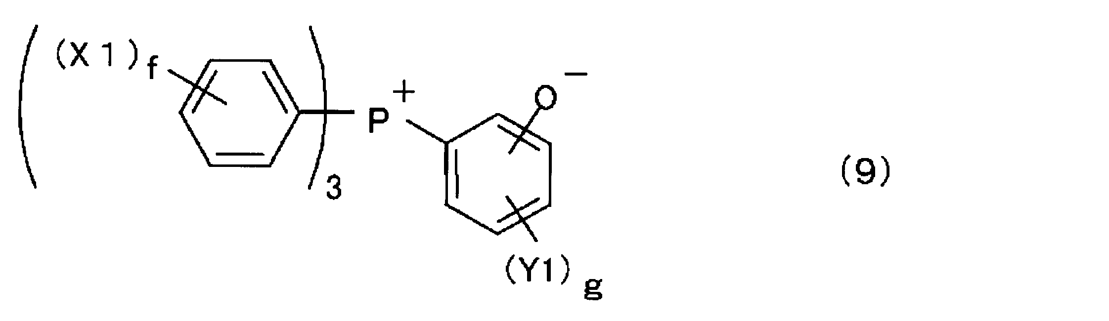
- Examples of the phosphobetaine compound that can be used in the semiconductor sealing resin composition of the present invention include compounds represented by the following general formula (9).
- X1 represents an alkyl group having 1 to 3 carbon atoms
- Y1 represents a hydroxyl group
- f is an integer of 0 to 5
- g is an integer of 0 to 4.
- f is an integer of 2 or more and the aromatic ring has a plurality of X1 as substituents
- the plurality of X1 may be the same as or different from each other.
- the compound represented by the general formula (9) is obtained as follows, for example. First, it is obtained through a step of bringing a triaromatic substituted phosphine, which is a third phosphine, into contact with a diazonium salt and replacing the triaromatic substituted phosphine with a diazonium group of the diazonium salt.
- a triaromatic substituted phosphine which is a third phosphine
- the present invention is not limited to this.
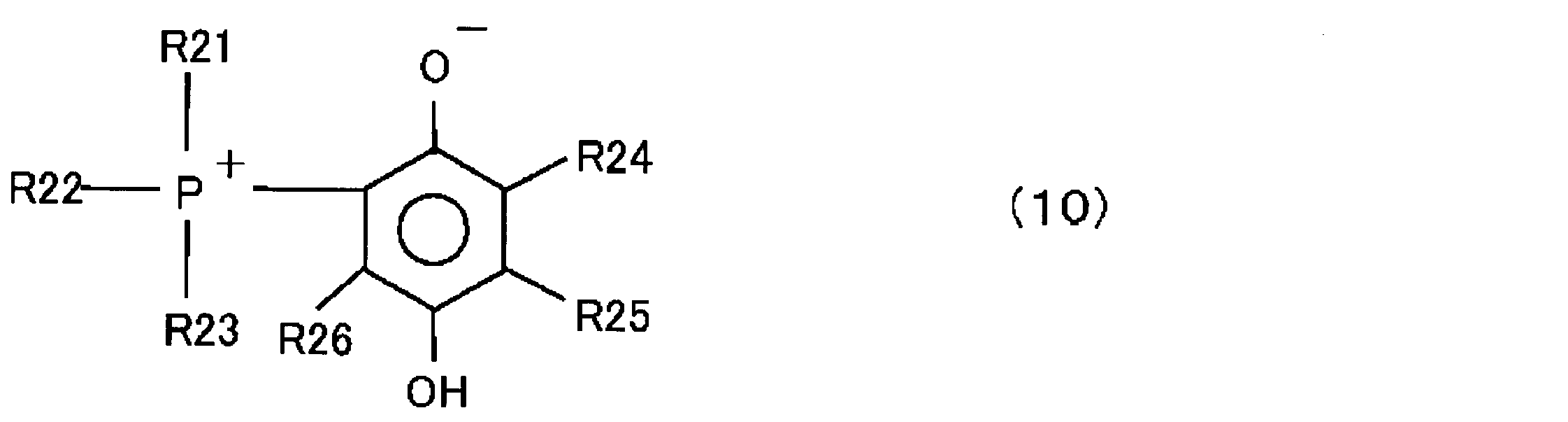
- Examples of the adduct of a phosphine compound and a quinone compound that can be used in the semiconductor sealing resin composition of the present invention include compounds represented by the following general formula (10).
- P represents a phosphorus atom
- R21, R22 and R23 each independently represent an alkyl group having 1 to 12 carbon atoms or an aryl group having 6 to 12 carbon atoms
- R24, R25 and R26 independently of each other represents a hydrogen atom or a hydrocarbon group having 1 to 12 carbon atoms
- R24 and R25 may be bonded to each other to form a ring.
- Examples of the phosphine compound used as an adduct of a phosphine compound and a quinone compound include an aromatic ring such as triphenylphosphine, tris (alkylphenyl) phosphine, tris (alkoxyphenyl) phosphine, trinaphthylphosphine, and tris (benzyl) phosphine.
- aromatic ring such as triphenylphosphine, tris (alkylphenyl) phosphine, tris (alkoxyphenyl) phosphine, trinaphthylphosphine, and tris (benzyl) phosphine.
- Those having a substituent or a substituent such as an alkyl group or an alkoxyl group are preferred.
- Examples of the substituent such as an alkyl group and an alkoxyl group include those having 1 to 6 carbon atoms. From the viewpoint of availability, tripheny
- examples of the quinone compound used for the adduct of the phosphine compound and the quinone compound include o-benzoquinone, p-benzoquinone and anthraquinones, and among them, p-benzoquinone is preferable from the viewpoint of storage stability.
- the adduct can be obtained by contacting and mixing in a solvent capable of dissolving both organic tertiary phosphine and benzoquinone.
- the solvent is preferably a ketone such as acetone or methyl ethyl ketone, which has low solubility in the adduct.
- the present invention is not limited to this.
- R21, R22 and R23 bonded to the phosphorus atom are phenyl groups, and R24, R25 and R26 are hydrogen atoms, that is, 1,4-benzoquinone and triphenyl
- R24, R25 and R26 are hydrogen atoms, that is, 1,4-benzoquinone and triphenyl
- a compound to which phosphine has been added is preferable in that it reduces the thermal elastic modulus of the cured product of the resin composition for semiconductor encapsulation.
- Examples of the monocyclic amidine compound that can be used in the semiconductor sealing resin composition of the present invention include 2-methylimidazole, 2-ethyl-4-methylimidazole, 2-phenylimidazole, 2-phenyl-4- Examples include methylimidazole and 1-benzyl-2-methylimidazole.
- imidazole represented by the following general formula (11) is particularly preferable.
- R which is a substituent of the following general formula (11), is preferably an aryl group such as a phenyl group or a tolyl group, an alkyl group such as a methyl group, an ethyl group, a propyl group or an isopropyl group, or an aralkyl group such as a benzyl group.
- R is hydrogen or a hydrocarbon group having 10 or less carbon atoms, and may be the same or different from each other.
- the lower limit of the content of the curing accelerator (D) that can be used in the resin composition for semiconductor encapsulation of the present invention is 0.01% with respect to 100% by mass of the total value of the resin composition for semiconductor encapsulation.
- the content is preferably at least mass%, more preferably at least 0.03% by mass, and most preferably at least 0.05 mass%.
- the upper limit of content of a hardening accelerator (D) is 1.5 mass% or less with respect to 100 mass% of total values of the resin composition for all semiconductor sealing, and 1.2 mass % Or less is more preferable, and 0.8% by mass or less is most preferable. Sufficient fluidity
- a compound (E) in which a hydroxyl group is bonded to each of two or more adjacent carbon atoms constituting an aromatic ring (hereinafter also simply referred to as “compound (E)”) can be used.
- the reason for using the compound (E) in which a hydroxyl group is bonded to each of two or more adjacent carbon atoms constituting the aromatic ring is to cure the epoxy resin (A) and the phenol resin-based curing agent (B). Even when a phosphorus atom-containing curing accelerator having no latency is used as the accelerator (D), the reaction during melt-kneading of the resin composition for semiconductor encapsulation can be suppressed, and the semiconductor encapsulation can be stably performed.
- the compound (E) also has an effect of lowering the melt viscosity of the resin composition for semiconductor encapsulation and improving the fluidity.
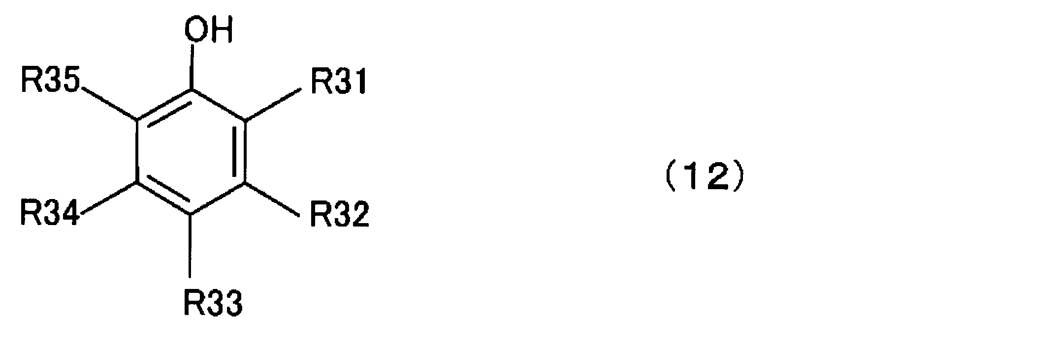
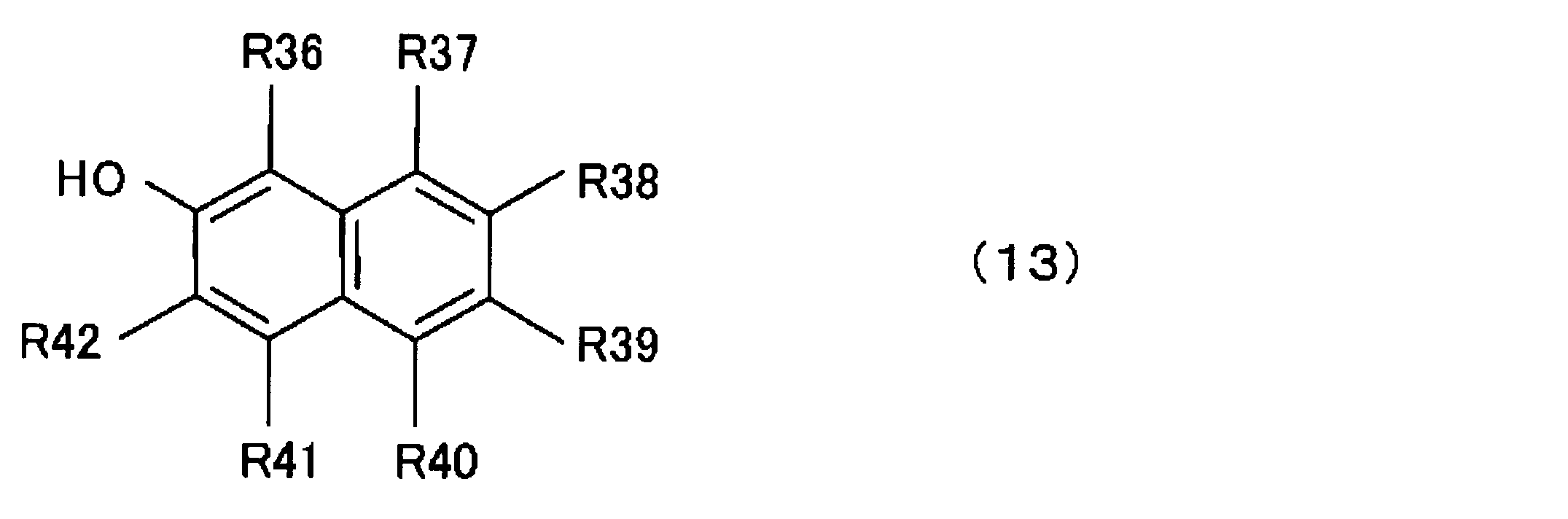
- a monocyclic compound represented by the following general formula (12) or a polycyclic compound represented by the following general formula (13) can be used. It may further have a substituent.
- one of R31 and R35 is a hydroxyl group, the other is a hydrogen atom, a hydroxyl group, or a substituent other than a hydroxyl group, and R32, R33, and R34 are substitutions other than a hydrogen atom, a hydroxyl group, or a hydroxyl group. It is a group.
- one of R36 and R42 is a hydroxyl group, the other is a hydrogen atom, a hydroxyl group or a substituent other than a hydroxyl group, and R37, R38, R39, R40, and R41 are a hydrogen atom, a hydroxyl group, A substituent other than a hydroxyl group.
- the monocyclic compound represented by the general formula (12) include catechol, pyrogallol, gallic acid, gallic acid ester, and derivatives thereof.
- Specific examples of the polycyclic compound represented by the general formula (13) include 1,2-dihydroxynaphthalene, 2,3-dihydroxynaphthalene, and derivatives thereof.
- a compound in which a hydroxyl group is bonded to each of two adjacent carbon atoms constituting an aromatic ring is preferable because of easy control of fluidity and curability.
- the mother nucleus is a compound having a low volatility and a highly stable weighing naphthalene ring.
- the compound (E) can be a compound having a naphthalene ring such as 1,2-dihydroxynaphthalene, 2,3-dihydroxynaphthalene and derivatives thereof.
- These compounds (E) may be used individually by 1 type, or may use 2 or more types together.
- the lower limit of the content of the compound (E) is preferably 0.01% by mass or more, more preferably 0.03% by mass with respect to 100% by mass of the total value of the resin composition for encapsulating all semiconductors. As mentioned above, it is 0.05 mass% or more especially preferably.
- the upper limit of content of a compound (E) is 1 mass% or less with respect to the total value of 100 mass% of the resin composition for all semiconductor sealing, More preferably, it is 0.8 mass%. Hereinafter, it is particularly preferably 0.5% by mass or less.
- a coupling agent (F) such as a silane coupling agent is added to improve the adhesion between the epoxy resin (A) and the inorganic filler (C).
- a coupling agent (F) if it reacts between an epoxy resin (A) and an inorganic filler (C) and improves the interface strength of an epoxy resin (A) and an inorganic filler (C).
- Well not particularly limited, for example, epoxy silane, amino silane, ureido silane, mercapto silane and the like.
- a coupling agent (F) raises the effect of the compound (E) of reducing the melt viscosity of the resin composition for semiconductor sealing, and improving fluidity
- Examples of the epoxy silane include ⁇ -glycidoxypropyltriethoxysilane, ⁇ -glycidoxypropyltrimethoxysilane, ⁇ -glycidoxypropylmethyldimethoxysilane, and ⁇ - (3,4 epoxycyclohexyl) ethyltrimethoxysilane.
- Examples of aminosilane include ⁇ -aminopropyltriethoxysilane, ⁇ -aminopropyltrimethoxysilane, N- ⁇ (aminoethyl) ⁇ -aminopropyltrimethoxysilane, and N- ⁇ (aminoethyl) ⁇ -aminopropyl.
- Methyldimethoxysilane N-phenyl ⁇ -aminopropyltriethoxysilane, N-phenyl ⁇ -aminopropyltrimethoxysilane, N- ⁇ (aminoethyl) ⁇ -aminopropyltriethoxysilane, N-6- (aminohexyl) 3 -Aminopropyltrimethoxysilane, N- (3- (trimethoxysilylpropyl) -1,3-benzenedimethanane, etc.
- ureidosilane include ⁇ -ureidopropyltriethoxysilane, hexa Methyl disilazane, etc.
- the primary amino moiety may be used as a latent aminosilane coupling agent protected by reacting with a ketone or an aldehyde, and the aminosilane may have a secondary amino group.
- a latent aminosilane coupling agent protected by reacting with a ketone or an aldehyde
- the aminosilane may have a secondary amino group.
- pyrolysis such as ⁇ -mercaptopropyltrimethoxysilane, 3-mercaptopropylmethyldimethoxysilane, bis (3-triethoxysilylpropyl) tetrasulfide, bis (3-triethoxysilylpropyl) disulfide
- Examples include silane coupling agents that exhibit the same function as mercaptosilane coupling agents, etc. These silane coupling agents may be pre-hydrolyzed, and these silane coupling agents. Can be used alone or two or more It may be used in combination.
- Mercaptosilane is preferred in terms of the balance between solder resistance and continuous moldability, aminosilane is preferred in terms of fluidity, and in terms of adhesion to organic components such as polyimide on the silicon chip surface and solder resist on the substrate surface. Epoxysilane is preferred.
- the total value of all the semiconductor sealing resin compositions is 100% by mass. Is preferably 0.01% by mass or more, more preferably 0.05% by mass or more, and particularly preferably 0.1% by mass or more. If the lower limit of the content of the coupling agent (F) such as a silane coupling agent is within the above range, the interface strength between the epoxy resin (A) and the inorganic filler (C) does not decrease, and the semiconductor Good solder crack resistance in the apparatus can be obtained.
- an upper limit of content of coupling agents (F), such as a silane coupling agent 1 mass% or less is preferable with respect to the total value of 100 mass% of the resin composition for whole semiconductor sealing, More preferably Is 0.8% by mass or less, particularly preferably 0.6% by mass or less. If the upper limit of the content of the coupling agent (F) such as a silane coupling agent is within the above range, the interface strength between the epoxy resin (A) and the inorganic filler (C) does not decrease, and the semiconductor Good solder crack resistance in the apparatus can be obtained.
- a silane coupling agent 1 mass% or less is preferable with respect to the total value of 100 mass% of the resin composition for whole semiconductor sealing, More preferably Is 0.8% by mass or less, particularly preferably 0.6% by mass or less.
- an inorganic flame retardant (G) can be added in order to improve flame retardancy.
- a metal hydroxide or a composite metal hydroxide that inhibits the combustion reaction by dehydrating and absorbing heat during combustion is preferable in that the combustion time can be shortened.
- the metal hydroxide include aluminum hydroxide, magnesium hydroxide, calcium hydroxide, barium hydroxide, and zirconia hydroxide.
- the composite metal hydroxide is a hydrotalcite compound containing two or more metal elements, wherein at least one metal element is magnesium, and the other metal elements are calcium, aluminum, tin, titanium, iron Any metal element selected from cobalt, nickel, copper, or zinc may be used, and as such a composite metal hydroxide, a magnesium hydroxide / zinc solid solution is easily available on the market.
- aluminum hydroxide and magnesium hydroxide / zinc solid solution are preferable from the viewpoint of the balance between solder resistance and continuous moldability.
- An inorganic flame retardant (G) may be used independently or may be used 2 or more types. Further, for the purpose of reducing the influence on the continuous moldability, a surface treatment may be performed with a silicon compound such as a silane coupling agent or an aliphatic compound such as wax.
- colorants such as carbon black, bengara and titanium oxide; natural waxes such as carnauba wax; synthetic waxes such as polyethylene wax; stearic acid and zinc stearate Release agents such as higher fatty acids and their metal salts or paraffin; low-stress additives such as silicone oil and silicone rubber may be appropriately blended.
- the resin composition for encapsulating a semiconductor of the present invention comprises an epoxy resin (A), a curing agent (B), an inorganic filler (C), and other additives described above at room temperature using, for example, a mixer. Mix uniformly and then melt and knead using a kneader such as a heating roll, kneader, or extruder, if necessary, and then cool and pulverize as necessary to achieve the desired degree of dispersion and fluidity. Etc. can be adjusted.
- a kneader such as a heating roll, kneader, or extruder
- the saturated ion viscosity of the resin composition for semiconductor encapsulation when measured under the conditions of a measurement temperature of 125 ° C. and a measurement frequency of 100 Hz using a dielectric analyzer. Is preferably 100 seconds or more, more preferably 180 seconds or more, and even more preferably 300 seconds or more from the start of measurement, while preferably 900 seconds or less, more preferably 800 seconds or less, still more preferably 700 seconds or less.
- the time when the saturated ion viscosity is reached means, for example, the time when the increase in the ion viscosity is stopped.
- the minimum ionic viscosity of the resin composition for semiconductor encapsulation when measured under the conditions of a measurement temperature of 125 ° C. and a measurement frequency of 100 Hz using a dielectric analyzer.
- Log Ion Viscosity is preferably 6 or more and 8 or less, and the ionic viscosity after 600 seconds from the start of measurement is preferably 9 or more and 11 or less.
- the time of appearance of the lowest ionic viscosity represents the ease of dissolution as a resin system, and the value of the lowest ionic viscosity represents the lowest viscosity as a resin system.
- the resin composition for semiconductor encapsulation according to the present invention, a nozzle having a nozzle diameter of 0.5 mm ⁇ and a length of 1 mm is used by using a Koka type viscosity measuring apparatus (manufactured by Shimadzu Corporation, CFT500).
- the high viscosity of the resin composition for semiconductor encapsulation when measured at a measurement temperature of 125 ° C. and a load of 40 kg is preferably 20 Pa ⁇ s to 200 Pa ⁇ s, more preferably 30 Pa ⁇ s to 180 Pa. -S or less.
- the curing accelerator (D) is appropriately selected, or a triphenolmethane type epoxy resin, a triphenolpropane type epoxy resin, an alkyl-modified triphenolmethane type epoxy resin, etc.
- Semiconductors with excellent low-temperature moldability by using polyfunctional epoxy resins and trifunctional phenolic resins such as triphenolmethane type phenolic resin, triphenolpropane type phenolic resin, and alkyl-modified triphenolmethane type phenolic resin
- a sealing resin composition is obtained.
- the step of forming the encapsulant layer 108 is preferably 100 ° C. or higher and 150 ° C. or lower, more preferably 115.
- the curing treatment can be performed under a temperature condition of not lower than 135 ° C and not higher than 135 ° C, more preferably not lower than 120 ° C and not higher than 130 ° C.
- the present inventors have found that if the molding temperature of the resin composition for semiconductor encapsulation is lowered, the residue is reduced.
- the residue of the mount film 104 can be reduced by setting the curing treatment of the semiconductor sealing resin composition within the above temperature range, that is, by reducing the curing temperature. Accordingly, by setting the molding temperature in the step of forming the sealing material layer 108 to be equal to or lower than the above upper limit value, the residue can be reduced. On the other hand, the moldability of the sealing material layer 108 can be improved by setting the molding temperature to the above lower limit value or more. In particular, by setting the molding temperature within a more preferable range, it is possible to realize a semiconductor device that is excellent in the balance between the reduction of residue and the moldability of the sealing material layer 108.
- the method for obtaining a granular semiconductor sealing resin composition according to the present invention is not particularly limited as long as the particle size distribution and granule density of the present invention are satisfied.
- a cylinder having a plurality of small holes The melt-kneaded resin composition is supplied to the inside of the rotor composed of the outer periphery of the disk and the disk-shaped bottom surface, and the semiconductor sealing resin composition is subjected to centrifugal force obtained by rotating the rotor.
- a method obtained by passing through small holes (hereinafter also referred to as “centrifugal milling method”); after each raw material component is premixed by a mixer, heated and kneaded by a kneader such as a roll, a kneader or an extruder, and then cooled and pulverized Through which a coarse product and a fine powder are removed from the pulverized product using a sieve (hereinafter, also referred to as “pulverized sieving method”); After that, a plurality of small diameters are arranged at the screw tip.
- the particle size distribution and granule density of the present invention can be obtained by selecting kneading conditions, centrifugal conditions, sieving conditions, cutting conditions and the like.
- a particularly preferred production method is centrifugal milling, and the granular semiconductor sealing resin composition obtained thereby can stably express the particle size distribution and granule density of the present invention. It is preferable for transportability and prevention of sticking.
- the particle surface can be smoothed to some extent, so that the particles are not caught and the frictional resistance with the surface of the conveying path does not increase, and the bridge ( This is also preferable for prevention of clogging) and prevention of retention on the conveyance path.
- particles are formed using centrifugal force from the state where the resin composition is melted, and therefore, the voids are included to some extent in the particles. As a result, the granule density can be lowered to some extent, which is advantageous in terms of transportability in compression molding.
- the pulverization sieving method expresses the particle size distribution of the present invention, such as selection of sheet thickness when forming a molten resin sheet before pulverization, selection of pulverization conditions and screen during pulverization, selection of sieving during sieving, etc. Since there are many factors that can be controlled independently, it is preferable in that there are many choices of means for adjusting to a desired particle size distribution.
- the hot cut method is also preferable in that a conventional production line can be used as it is, for example, by adding a hot cut mechanism to the tip of the extruder.
- FIG. 6 is a schematic view of an example from the melt kneading of the semiconductor sealing resin composition to the collection of the granular semiconductor sealing resin composition to obtain the granular semiconductor sealing resin composition.
- FIG. 7 is a cross-sectional view of an embodiment of an exciting coil for heating the rotor and the cylindrical outer peripheral portion of the rotor, and
- FIG. 8 is a melt-kneaded resin composition for semiconductor encapsulation supplied to the rotor. Sectional drawing of one Example of the double tube
- the semiconductor sealing resin composition melt-kneaded by the twin-screw extruder 309 is supplied to the inside of the rotor 301 through a double-pipe cylindrical body 305 cooled by passing a refrigerant between the inner wall and the outer wall.
- the double-pipe cylinder 305 is preferably cooled using a refrigerant so that the melt-kneaded resin composition for semiconductor sealing does not adhere to the wall of the double-pipe cylinder 305.
- the semiconductor sealing resin composition when the semiconductor sealing resin composition is supplied to the rotor 301 through the double-pipe cylindrical body 305, even if the semiconductor sealing resin composition is supplied in a continuous thread shape, the rotor 301 The semiconductor sealing resin composition does not overflow from the rotor 301 during high-speed rotation, and stable supply becomes possible.
- the particle shape and particle size distribution of the granular semiconductor sealing resin composition can be adjusted by controlling the molten resin discharge temperature and the like according to the kneading conditions in the twin screw extruder 309. Further, by incorporating a degassing device in the twin-screw extruder 309, the entrainment of bubbles in the particles can be controlled.
- the rotor 301 is connected to a motor 310 and can be rotated at an arbitrary number of revolutions. By appropriately selecting the number of rotations, the particle shape and particle size distribution of the granular resin composition for encapsulating a semiconductor can be adjusted.
- a cylindrical outer peripheral portion 302 having a plurality of small holes installed on the outer periphery of the rotor 301 includes a magnetic material 303. Magnetic material due to eddy current loss and hysteresis loss caused by passing alternating magnetic flux generated by passing the AC power generated by the AC power generator 306 through the magnetic material 303 to the exciting coil 304 provided in the vicinity thereof. 303 is heated. In addition, as this magnetic material 303, iron material, silicon steel, etc.
- the vicinity of the small holes in the cylindrical outer peripheral portion 302 having a plurality of small holes may not be formed of the same material as the magnetic material 303.
- the vicinity of the small hole of the cylindrical outer peripheral portion 302 is formed of a nonmagnetic material having a high thermal conductivity, and the magnetic material 303 is provided above and below the cylindrical outer peripheral portion 302.
- the vicinity of the small holes 302 can also be heated.
- the nonmagnetic material include copper and aluminum, and one type or two or more types of nonmagnetic materials can be used in combination.
- the resin composition for encapsulating a semiconductor in contact with the heated cylindrical outer peripheral portion 302 having a plurality of small holes easily passes through the small holes in the cylindrical outer peripheral portion 302 and is discharged without increasing the melt viscosity.
- the temperature to heat can be arbitrarily set with the characteristic of the resin composition for semiconductor sealing to apply. By appropriately selecting the heating temperature, it is possible to adjust the particle shape and particle size distribution of the granular semiconductor sealing resin composition. In general, if the heating temperature is raised too much, the resin composition hardens, and the fluidity may decrease or the small holes in the cylindrical outer periphery 302 may clog.
- the contact time of the resin composition for semiconductor encapsulation and the cylindrical outer peripheral portion 302 is extremely short, the influence on the fluidity is extremely small. Further, since the cylindrical outer peripheral portion 302 having a plurality of small holes is uniformly heated, there is very little local change in fluidity. The plurality of small holes in the cylindrical outer peripheral portion 302 can adjust the particle shape and particle size distribution of the granular semiconductor sealing resin composition by appropriately selecting the hole diameter.
- the granular semiconductor sealing resin composition discharged through the small holes in the cylindrical outer peripheral portion 302 is collected, for example, in an outer tank 308 installed around the rotor 301.
- the outer tank 308 has small holes in the cylindrical outer peripheral portion 302 in order to prevent adhesion of the granular semiconductor sealing resin composition to the inner wall and fusion between the granular semiconductor sealing resin compositions.
- the collision surface where the granular semiconductor sealing resin composition flying through and collides with the inner wall has an impact surface of 10 to 80 degrees with respect to the flight direction of the granular semiconductor sealing resin composition, preferably 25. It is preferably installed with an inclination of ⁇ 65 degrees.
- the slope of the collision surface with respect to the flight direction of the resin composition for semiconductor encapsulation is not more than the above upper limit value, the collision energy of the granular resin composition for semiconductor encapsulation can be sufficiently dispersed, and adhesion to the wall surface is prevented. Less likely to occur. Further, if the slope of the collision surface with respect to the flight direction of the resin composition is equal to or higher than the lower limit value, the flight speed of the granular semiconductor sealing resin composition can be sufficiently reduced. Even in the event of a next collision, there is little risk of adhering to the exterior wall surface.
- the inner diameter of the outer tank 308 is such that the granular semiconductor sealing resin composition is sufficiently cooled to adhere to the inner wall of the granular semiconductor sealing resin composition, or the granular semiconductor sealing resin composition. It is desirable to have a size that does not cause mutual fusion. In general, an air flow is generated by the rotation of the rotor 301 and a cooling effect is obtained, but cold air may be introduced as necessary.
- the size of the outer tank 308 depends on the amount of resin to be processed, for example, when the diameter of the rotor 301 is 20 cm, adhesion and fusion can be prevented if the inner diameter of the outer tank 308 is about 100 cm.
- the mount film 104 is peeled from the lower surface 30 of the sealing material layer 108 and the lower surface 20 of the semiconductor element 106.
- the mount film 104 can be separated by thermally decomposing the mount film 104 by heat treatment.
- an irradiation treatment such as electron beam or ultraviolet light may be performed.
- the mount film 104 and the carrier 102 can be separated from the structure including the carrier 102, the mount film 104, the semiconductor element 106, and the sealing material layer 108.
- the rewiring pseudo wafer 200 shown in FIG. 3B is obtained.
- the rewiring pseudo-wafer 200 includes a semiconductor element 106 and a sealing material layer 108. On the same surface as the lower surface 30 of the sealing material layer 108, the lower surfaces 20 (connection surfaces) of the plurality of semiconductor elements 106 are exposed. On the other hand, a sealing material layer 108 is formed so as to continuously cover the upper surfaces of the plurality of semiconductor elements 106. In other words, in a cross-sectional view, the sealing material layer 108 and the semiconductor element 106 are formed on one surface (rewiring forming surface) side of the rewiring pseudo-wafer 200, while on the other surface (sealing surface) side. Only the sealing material layer 108 is formed.
- the rewiring pseudo wafer 200 has, for example, a plate shape.
- the rewiring pseudo wafer 200 may have a circular shape or a rectangular shape in plan view.
- the peel strength between the sealing material layer 108 and the mount film 104 under the following measurement conditions is preferably 1 N / m or more and 10 N / m or less, More preferably, it is 2 N / m or more and 9 N / m or less.
- the measurement conditions for peel strength are a measurement temperature of 180 ° C. and a peeling speed of 50 mm / min.
- the upper limit value of the contact angle of the lower surface of the sealing material layer 108 after the step of peeling the mount film 104 is preferably 70 at the time of measurement using formamide. It is not more than 65 degrees, more preferably not more than 65 degrees, and further preferably not more than 60 degrees.
- the lower limit value of the contact angle is not particularly limited, but is, for example, 0 degree, preferably 5 degrees or more, and more preferably 10 degrees or more.
- the contact angle may be, for example, an average value, a minimum value, or a maximum value after a predetermined measurement time from the start of measurement, but the average value is more preferable.
- predetermined time For example, it shall be 10 seconds.
- a method of taking the average value by repeating the measurement of the value after 10 seconds by allowing the droplet to stand at 25 ° C. and measuring the value after 10 seconds can be mentioned.
- This formamide is used as a standard solution in general contact angle measurement.
- the measurement is performed at a measurement temperature of 25 ° C. and a measurement apparatus: Dropmaster 500 (manufactured by Kyowa Science Co., Ltd.).
- the contact angle can be reduced by appropriately selecting the main agent and the curing agent or appropriately selecting the curing accelerator (D).
- a reduction in the contact angle measured using formamide indicates that the contact angle of the rewiring material is reduced.
- the residue of the mount film 104 is reduced, so that the liquid rewiring material spreads on the surface of the rewiring pseudo wafer 200. It is suppressed that it becomes difficult. Therefore, in the present embodiment, the semiconductor device 100 with excellent yield can be obtained.
- Post-cure may be performed on the sealing material layer 108 in the rewiring pseudo-wafer 200 before and / or after the mount film 104 is peeled off. Post-curing is performed, for example, in a temperature range of 150 ° C. to 200 ° C., more preferably 160 ° C. to 190 ° C., for 10 minutes to 8 hours. By performing the post cure after the mount film 104 is peeled off, the residue of the mount film 104 can be suppressed.
- a rewiring insulating resin layer 110 is formed on the lower surface 30 of the sealing material layer 108 and on the lower surface 20 of the semiconductor element 106. .
- the rewiring insulating resin layer 110 is formed on one surface of the rewiring pseudo wafer 200 (the surface having the connection surface of the semiconductor element 106).
- an opening 112 exposing the surface of the pad 122 on the connection surface of the semiconductor element 106 is formed in the insulating resin layer 110 for rewiring.
- a pattern is formed in the insulating resin layer 110 for rewiring using a photolithography method or the like, and a curing process is performed.
- the curing is performed in a temperature range of 150 ° C. to 300 ° C. for 10 minutes to 5 hours.
- the rewiring insulating resin layer 110 may be directly formed on the rewiring pseudo-wafer 200, but a passivation layer (not shown) may be formed therebetween.
- the insulating resin layer 110 for rewiring is not particularly limited, but polyimide resin, polybenzooxide resin, benzocyclobutene resin and the like are used from the viewpoint of heat resistance and reliability.
- a resist layer is formed on the power feeding layer and exposed to a predetermined pattern.
- the via 114 and the rewiring circuit 116 are formed by electrolytic copper plating.
- the resist layer is peeled off and the power feeding layer is etched.
- the Shore D hardness of the sealing material layer 108 after being cured at 125 ° C. for 10 minutes is preferably 70 or more and 100 or less. Preferably they are 80 or more and 95 or less.
- the bending strength of the sealing material layer 108 at 260 ° C. is preferably 10 MPa or more and 100 MPa or less, and more preferably 20 MPa or more and 80 MPa or less. .
- a sample having a stable shape can be prepared in the sealing material layer 108 around the semiconductor element 106, and the occurrence of deformation of the surface shape such as a dent can be suppressed.
- the resin layer 110 and the rewiring circuit 116 can be formed with high accuracy.
- the flexural modulus of the sealing material layer 108 at 260 ° C. is preferably 5 ⁇ 10 2 MPa or more and 3 ⁇ 10 3 MPa or less, more preferably. Is 7 ⁇ 10 2 MPa or more and 2.8 ⁇ 10 3 MPa or less.
- the encapsulant layer 108 is stored when measured using a dynamic viscoelasticity measuring device at a three-point bending mode, a frequency of 10 Hz, and a measurement temperature of 260 ° C.
- the elastic modulus (E ′) is preferably 5 ⁇ 10 2 MPa or more and 5 ⁇ 10 3 MPa or less, more preferably 8 ⁇ 10 2 MPa or more and 4 ⁇ 10 3 MPa or less.
- the linear expansion coefficient ( ⁇ 1) in the xy plane direction of the sealing material layer 108 in the region of 25 ° C. or more and the glass transition temperature (Tg) or less is preferably Is from 3 ppm / ° C. to 15 ppm / ° C., more preferably from 4 ppm / ° C. to 11 ppm / ° C.
- Tg glass transition temperature
- the linear expansion coefficient ( ⁇ 1) can be within the above range.
- the sealing material layer 108 around the semiconductor element 106 can be prevented from warping the opposing surface side with respect to the arrangement surface side of the semiconductor element 106.
- the insulating resin layer 110 for wiring and the rewiring circuit 116 can be formed with high accuracy.
- a polyfunctional epoxy resin such as a triphenolmethane type epoxy resin, a triphenolpropane type epoxy resin, an alkyl-modified triphenolmethane type epoxy resin, and a triphenolmethane type phenol resin.
- polyfunctional phenolic resins such as triphenolpropane type phenolic resin and alkyl-modified triphenolmethane type phenolic resin, or by promoting curing during molding or post-curing after molding (post By curing, it becomes possible to further cure the resin, and a cured product (encapsulant layer 108) of the resin composition for semiconductor encapsulation having a stable shape can be obtained. Therefore, the yield of the semiconductor device 100 of this embodiment is improved.
- the glass transition temperature (Tg) of the sealing material layer 108 is preferably 100 ° C. or higher and 250 ° C. or lower, more preferably 110 ° C. or higher and 220 ° C. or lower. It is.
- the glass transition temperature (Tg) can be within the above range by using a polyfunctional epoxy resin (A) or a polyfunctional curing agent (B) or by promoting a curing reaction.
- the rewiring insulating resin layer 110 when the rewiring insulating resin layer 110 is cured at 250 ° C. for 90 minutes, the rewiring insulating resin layer 110 is cured before and after the curing process.
- the mass difference of the sealing material layer 108 is preferably within 5% by mass.
- solder ball 120 is mounted on the land by mounting the solder ball 120 and then melting by heating. Further, a solder resist layer 118 is formed so as to cover a part of the rewiring circuit 116 and the solder balls 120.
- the applied flux can be resin-based or water-based.
- the heating and melting method reflow, hot plate (hot plate) or the like can be used. Thereby, the wafer level package 210 is obtained. Thereafter, the wafer level package 210 is singulated, for example, for each semiconductor element 106 by a method such as dicing. Thereby, the semiconductor device 100 of the present embodiment can be obtained.
- the semiconductor element 106 having a plurality of functions can be arranged in one semiconductor device 100 by dividing the semiconductor chip 108 into units.
- the semiconductor device 100 obtained in this way may be mounted on a substrate (interposer).
- the solder ball 120 of the semiconductor device 100 and a wiring circuit formed on the interposer are electrically connected via bumps. Thereby, a stacked package is obtained.
- each component used for the resin composition for semiconductor sealing obtained in the Example and comparative example which are mentioned later is demonstrated. Unless otherwise specified, the amount of each component is part by mass.
- Example 1 Composition (part by mass) of resin composition for semiconductor encapsulation>
- Epoxy resin 1 an epoxy resin mainly composed of an epoxy resin having a triphenylmethane skeleton represented by the following formula (1) (product name: YL6677, epoxy equivalent 163) 6.95 parts by mass
- Phenol resin-based curing agent 1 phenol resin having a triphenylmethane skeleton represented by the following formula (2) (manufactured by Air Water Co., Ltd., trade name HE910-20, softening point 88 ° C., hydroxyl group equivalent 101) 4.30 parts by mass Fused spherical silica 1: (average particle size 24 ⁇ m, specific surface area 3.5 m 2 / g) 73 parts by mass Fused spherical silica 2: (average particle size 0.5 ⁇ m, specific surface area 5.9 m 2 / g) 15 parts by mass
- Agent 1 Triphenylphosphine (manufactured by Kay Chemical Co
- An iron punched wire net having a small hole with a hole diameter of 2.5 mm was used as the material of the cylindrical outer peripheral portion 302 shown in FIG.
- a punched wire net having a height of 25 mm and a thickness of 1.5 mm processed into a cylindrical shape was attached to the outer periphery of a rotor 301 having a diameter of 20 cm, thereby forming a cylindrical outer peripheral portion 302.
- the rotor 301 was rotated at 3000 RPM, and the cylindrical outer peripheral portion 302 was heated to 115 ° C. with an exciting coil.
- the melt obtained by melting and kneading the master batch with the twin-screw extruder 309 while degassing with a degassing device was supplied to the inside of the rotor 301 at a rate of 2 kg / hr through the double-pipe cylindrical body 305 from above the rotor 301.
- the granular resin composition for semiconductor sealing was obtained by allowing the melt to pass through the plurality of small holes in the cylindrical outer peripheral portion 302 by centrifugal force obtained by rotating the rotor 301.
- a plurality of semiconductor elements were arranged side by side on a mount film (manufactured by Nitto Denko Corporation: Riva Alpha (registered trademark)). Subsequently, compression molding was performed using the granular semiconductor sealing resin composition to seal the semiconductor element on the mount film.
- the compression molding conditions were a molding temperature of 125 ° C. and a curing time of 7 minutes. Thereafter, post-curing was performed at 150 ° C. for 1 hour, the mount film was peeled off, and further post-curing was performed at 175 ° C. for 4 hours.
- a rewiring material manufactured by Sumitomo Bakelite Co., Ltd., CRC-8902
- CRC-8902 a rewiring material
- Examples 2 to 6 Comparative Examples 1 to 4
- a granular resin composition was produced in the same manner as in Example 1 according to the formulation shown in Table 1, and then a semiconductor device was produced in the same manner as in Example 1.
- the raw materials used other than Example 1 are shown below.
- Epoxy resin 2 phenol aralkyl type epoxy resin having a biphenylene skeleton represented by the following formula (3) (manufactured by Nippon Kayaku Co., Ltd., trade name NC3000P, softening point 58 ° C., epoxy equivalent 273)
- Phenol resin curing agent 2 Phenol aralkyl resin having a biphenylene skeleton represented by the following formula (4) (Maywa Kasei Co., Ltd., trade name MEH-7851SS, softening point 107 ° C., hydroxyl equivalent 204)
- Curing accelerator 2 4-hydroxy-2- (triphenylphosphonium) phenolate (manufactured by Kay Kasei Co., Ltd., trade name TPP-BQ)
- Curing accelerator 3 Tetraphenylphosphonium bis (naphthalene-2,3-dioxy) phenyl silicate (manufactured by Sumitomo Bakelite Co., Ltd.)
- Tg -Glass transition temperature
- ⁇ 1 linear expansion coefficient by TMA measurement (molded product at 125 ° C)
- Transfer molding was performed using the granular resin compositions obtained in Examples and Comparative Examples to obtain test pieces having a length of 15 mm, a width of 4 mm, and a thickness of 3 mm.
- the conditions for transfer molding were a molding temperature of 125 ° C. and a curing time of 7 minutes.
- the obtained test piece was heated from a room temperature (25 ° C.) at a heating rate of 5 ° C./min using a thermal dilatometer (TMA-120 manufactured by Seiko Instruments Inc.). The rapidly changing temperature was determined as the glass transition temperature.
- the unit is ° C.
- an average linear expansion coefficient between room temperature (25 ° C.) and Tg-30 ° C. was obtained and set as ⁇ 1.
- the unit is ppm / ° C.
- the measurement results are shown in Table 2.
- Peel strength In the manufacturing process of the semiconductor device of the example and the comparative example, when the mount film is peeled off, the sealing material layer and the mount film are peeled off at a measurement temperature of 180 ° C. and a peeling speed of 50 mm / min. The peel strength was determined. The unit is N / m. The measurement results are shown in Table 2.
- the present invention there is provided a structure of a semiconductor device with reduced yield and excellent yield, and a method for manufacturing the same. Therefore, the present invention can be suitably used for a semiconductor device and a manufacturing method thereof.
Landscapes
- Structures Or Materials For Encapsulating Or Coating Semiconductor Devices Or Solid State Devices (AREA)
- Encapsulation Of And Coatings For Semiconductor Or Solid State Devices (AREA)
- Epoxy Resins (AREA)
Abstract
Description
本願は、2011年3月10日に日本に出願された特願2011-053541号に基づき優先権を主張し、その内容をここに援用する。
[1]
熱剥離性粘着層の主面上に、複数の半導体素子を配置する工程と、
半導体封止用樹脂組成物を用いて、前記熱剥離性粘着層の前記主面上の複数の前記半導体素子を封止する封止材層を形成する工程と、
前記熱剥離性粘着層を剥離することにより、前記封止材層の下面および前記半導体素子の下面を露出させる工程と、を含み、
前記熱剥離性粘着層を剥離する前記工程の後における、前記封止材層の前記下面の接触角が、ホルムアミドを用いた測定時において、70度以下である、半導体装置の製造方法。
[2]
前記封止材層を形成する工程は、100℃以上150℃以下の温度条件で硬化処理を行う工程を含む、[1]に記載の半導体装置の製造方法。
[3]
前記熱剥離性粘着層を剥離する前記工程の後、前記封止材層の前記下面上および前記半導体素子の前記下面上に、再配線用絶縁樹脂層を形成する工程と、
前記再配線用絶縁樹脂層上に、再配線回路を形成する工程と、を含む、[1]または[2]に記載の半導体装置の製造方法。
[4]
前記熱剥離性粘着層を剥離する前記工程の後、前記再配線用絶縁樹脂層を形成する工程の前に、150℃以上200℃以下の温度条件で、更に硬化後処理を行う工程を含む、[3]に記載の半導体装置の製造方法。
[5]
前記封止材層を形成する前記工程において、顆粒の前記半導体封止用樹脂組成物を用い、圧縮形成を行うことにより、前記封止材層を形成する、[1]から[4]のいずれか1項に記載の半導体装置の製造方法。
[6]
誘電分析装置を用いて、測定温度125℃、測定周波数100Hzの条件で測定した際の、前記半導体封止用樹脂組成物の飽和イオン粘度に到達する時刻が、測定開始から100秒以上、900秒以下にある、[1]から[5]のいずれか1項に記載の半導体装置の製造方法。
[7]
測定温度180℃、引き剥がし速度50mm/minの条件で測定した際の、前記封止材層と前記マウントフィルムとのピール強度が1N/m以上、10N/m以下である、[1]から[6]のいずれか1項に記載の半導体装置の製造方法。
[8]
125℃、10分の条件で硬化させた後の前記封止材層のショアD硬度が70以上である、[1]から[7]のいずれか1項に記載の半導体装置の製造方法。
[9]
誘電分析装置を用いて、測定温度125℃、測定周波数100Hzの条件で測定した際の、前記半導体封止用樹脂組成物の最低イオン粘度が、6以上、8以下であり、かつ、測定開始からの経過時間が600秒後のイオン粘度が、9以上11以下である、[1]から[8]のいずれか1項に記載の半導体装置の製造方法。
[10]
高化式粘度測定装置を用いて、測定温度125℃、荷重40kgで測定した際の、前記半導体封止用樹脂組成物の高化式粘度が、20Pa・s以上200Pa・s以下である、[1]から[9]のいずれか1項に記載の半導体装置の製造方法。
[11]
260℃における、前記封止材層の曲げ強度が、10MPa以上、100MPa以下である、[1]から[10]のいずれか1項に記載の半導体装置の製造方法。
[12]
260℃における、前記封止材層の曲げ弾性率が、5×10²MPa以上、3×10³MPa以下である、[1]から[11]のいずれか1項に記載の半導体装置の製造方法。
[13]
前記封止材層のガラス転移温度(Tg)が、100℃以上、250℃以下である、[1]から[12]のいずれか1項に記載の半導体装置の製造方法。
[14]
25℃以上、ガラス転移温度(Tg)以下の領域における、前記封止材層のxy平面方向の線膨張係数(α1)が、3ppm/℃以上、15ppm/℃以下である、[1]から[13]のいずれか1項に記載の半導体装置の製造方法。
[15]
動的粘弾性測定器を用い、三点曲げモード、周波数10Hz、測定温度260℃で測定した際の、前記封止材層の貯蔵弾性率(E')が、5×10²MPa以上、5×10³MPa以下である、[1]から[14]のいずれか1項に記載の半導体装置の製造方法。
[16]
前記再配線用絶縁樹脂層を形成する前記工程において、前記再配線用絶縁樹脂層を250℃、90分で硬化させたとき、前記再配線用絶縁樹脂層の硬化処理前と硬化処理後との前記封止材層の質量差が、5質量%以内である、[3]に記載の半導体装置の製造方法。
[17]
[1]から[16]のいずれか1項に記載の半導体装置の製造方法で得られた、半導体装置。
本実施の形態における半導体装置の製造方法は、以下の工程を含む。
(チップマウント工程):熱剥離性粘着層(マウントフィルム104)の主面10上に、複数の半導体素子106を配置する工程。
(封止材層108形成工程):半導体封止用樹脂組成物を用いて、マウントフィルム104の主面10上の複数の半導体素子106を封止する封止材層108を形成する工程。
(再配線用疑似ウエハ200形成工程):マウントフィルム104を剥離することにより、封止材層108の下面および半導体素子106の下面を露出させる工程。
また、本実施の形態における半導体装置の製造方法は、以下の工程を含む。
(再配線工程):熱剥離性粘着層(マウントフィルム104)を剥離する工程の後、封止材層108の下面30上および半導体素子106の下面20上に、再配線用絶縁樹脂層110を形成する工程と、再配線用絶縁樹脂層110上に、再配線回路116を形成する工程。
しかしながら、本発明者らが検討した結果、従来のエポキシ樹脂組成物の組成は、製造プロセスへの影響については特に意図せずに、最終製品の封止特性を求めて選択されているため、疑似ウエハの封止樹脂面からマウントフィルムを剥離したときに、封止樹脂面上にマウントフィルムの一部が残るという、ノリ残りが発生することが判明した。このようなノリ残りが発生した疑似ウエハ面上に再配線材料を塗布すると、ノリ残りが再配線材料の濡れ拡がりを阻害することにより、再配線材料の塗膜特性が低下することがあり得た。このため、従来の半導体装置の製造方法では、歩留まりが低下することがあった。
上記実験事実に基づき、次の仮説を立てた。
(i)再配線材料の濡れ性の傾向を示す、接触角を測定する測定標準物質が存在すること。
(ii)(i)の測定標準物質により、かかる再配線材料の濡れ性を定性的に評価できること。
(iii)(i)の測定標準物質により測定された接触角を適切に制御することにより、再配線材料の濡れ性を改善できること。
こうした仮説に基づき、本発明者らは、再配線材料の濡れ性の傾向を示す測定標準物質を見出し、その測定標準物質による接触角を適切な値に制御することを検討した。
まず、図2(a)に示すように、板状のキャリア102上に、熱剥離性粘着層(マウントフィルム104)を配置する。例えば、キャリア102の表面上に、フィルム状のマウントフィルム104を載置することができる。
キャリア102の形状および材料としては、特に限定されないが、例えば、上面視において円形形状または多角形形状の金属板またはシリコン基板を用いることができる。
また、マウントフィルム104は、好ましくは主剤と発泡剤とを含む。この主剤としては、特に制限はなく、例えば、アクリル系粘着剤、ゴム系粘着剤、スチレン・共役ジエンブロック共重合体であり、好ましくはアクリル系粘着剤である。また、発泡剤としては、特に制限はなく、例えば、無機系、有機系等の各種発泡剤である。マウントフィルム104の熱剥離性は、例えば粘着剤を発泡性のものとすることによって得られており、この粘着剤が発泡する温度まで加熱すると、粘着剤の接着力が実質的になくなるため、マウントフィルム104を被着体から容易に剥離することができる。
続いて、図3(a)に示すように、マウントフィルム104の主面10上に載置された複数の半導体素子106を、封止材層108で封止する。すなわち、半導体素子106の側壁上および上面上に封止材層108を形成するとともに、半導体素子106同士の離間部を埋め込むように封止材層108を形成する。このため、半導体素子106の下面20(接続面)と封止材層108の下面30(マウントフィルム104剥離面)とは同一面を構成している。本実施の形態において、同一面とは、連続した面であり、かつ凹凸の高低差が好ましくは1mm以下、より好ましくは100μm以下のものを指す。このような封止材層108は、本発明に係る半導体封止用樹脂組成物を硬化することにより形成している。例えば、封止材層108は、顆粒の半導体封止用樹脂組成物を用い、圧縮成形を行うことによって形成することができる。
ここで、本発明に係る半導体封止用樹脂組成物の各成分等について説明する。
本発明に係る半導体封止用樹脂組成物は、少なくともエポキシ樹脂(A)と、硬化剤(B)と、無機充填剤(C)と、を含む。
次に、硬化剤(B)について説明する。硬化剤(B)は、特に限定されないが、たとえばフェノール樹脂とすることができる。このようなフェノール樹脂系硬化剤は、一分子内にフェノール性水酸基を2個以上、より好ましくは3個以上有するモノマー、オリゴマー、ポリマー全般であり、その分子量、分子構造を特に限定するものではない。例えば、フェノール樹脂系硬化剤として、フェノールノボラック樹脂、クレゾールノボラック樹脂、ナフトールノボラック樹脂等のノボラック型樹脂;トリフェノールメタン型フェノール樹脂等の多官能型フェノール樹脂;テルペン変性フェノール樹脂、ジシクロペンタジエン変性フェノール樹脂等の変性フェノール樹脂;フェニレン骨格及び/又はビフェニレン骨格を有するフェノールアラルキル樹脂、フェニレン及び/又はビフェニレン骨格を有するナフトールアラルキル樹脂等のアラルキル型樹脂;ビスフェノールA、ビスフェノールF等のビスフェノール化合物等が挙げられる。これらは、1種類を単独で用いても2種類以上を併用してもよい。このようなフェノール樹脂系硬化剤により、耐燃性、耐湿性、電気特性、硬化性、保存安定性等のバランスが良好となる。特に、硬化性の点から、たとえばフェノール樹脂系硬化剤の水酸基当量は、90g/eq以上、250g/eq以下とすることができる。
本発明の半導体封止用樹脂組成物に用いられる無機充填剤(C)としては、半導体封止用樹脂組成物の技術分野で一般的に用いられる無機充填剤を使用することができる。例えば、溶融シリカ、球状シリカ、結晶シリカ、アルミナ、窒化珪素、窒化アルミ等が挙げられる。無機充填剤の平均粒径は、金型キャビティへの充填性の観点から、0.01μm以上、150μm以下であることが望ましい。
本発明の半導体封止用樹脂組成物は、硬化促進剤(D)を含んでもよい。硬化促進剤(D)は、エポキシ樹脂(A)のエポキシ基とフェノール樹脂系硬化剤(B)の水酸基との反応を促進するものであればよく、一般に使用される硬化促進剤(D)を用いることができる。


ここで、本発明者らは、メカニズムは不明だが、半導体封止用樹脂組成物の成形温度を低くするとノリ残りが低減することを見出した。したがって、半導体封止用樹脂組成物の硬化処理を上記温度範囲内とすることにより、すなわち、硬化温度を低減することにより、マウントフィルム104のノリ残りを低減させることができる。
従って、封止材層108を形成する工程における成形温度を上記上限値以下とすることにより、ノリ残りを低減させることができる。一方、成形温度を上記下限値以上とすることにより、封止材層108の成形性を向上させることができる。とくに、成形温度をより好ましい範囲内とすることにより、ノリ残りの低減と封止材層108の成形性とのバランスに優れた半導体装置を実現することができる。
次に、本発明の顆粒状の半導体封止用樹脂組成物を得る方法について説明する。
本発明に係る顆粒状の半導体封止用樹脂組成物を得る方法としては、本発明の粒度分布や顆粒密度を満足すれば特に限定されるものではないが、例えば、複数の小孔を有する円筒状外周部と円盤状の底面から構成される回転子の内側に、溶融混練された樹脂組成物を供給し、その半導体封止用樹脂組成物を、回転子を回転させて得られる遠心力によって小孔に通過させて得る方法(以下、「遠心製粉法」とも言う。);各原料成分をミキサーで予備混合後、ロール、ニーダー又は押出機等の混練機により加熱混練後、冷却、粉砕工程を経て粉砕物とし、篩(ふるい)を用いて粉砕物から粗粒と微紛の除去を行って得る方法(以下、「粉砕篩分法」とも言う。);各原料成分をミキサーで予備混合後、スクリュー先端部に小径を複数配置したダイを設置した押出機を用いて、加熱混練を行うとともに、ダイに配置された小孔からストランド状に押し出されてくる溶融樹脂をダイ面に略平行に摺動回転するカッターで切断して得る方法(以下、「ホットカット法」とも言う。)等が挙げられる。いずれの方法でも混練条件、遠心条件、篩分条件、切断条件等を選ぶことにより本発明の粒度分布や顆粒密度を得ることができる。特に好ましい製法としては、遠心製粉法であり、これにより得られる顆粒状の半導体封止用樹脂組成物は、本発明の粒度分布や顆粒密度を安定して発現させることができるため、搬送路上での搬送性や固着防止に対して好ましい。また、遠心製粉法では、粒子表面をある程度滑らかにすることができるため、粒子同士が引っかかったり、搬送路面との摩擦抵抗が大きくなったりすることもなく、搬送路への供給口でのブリッジ(詰まり)の防止、搬送路上での滞留の防止に対しても好ましい。また、遠心製粉法では、樹脂組成物が溶融した状態から遠心力を用いて粒子を形成させるため、粒子内に空隙がある程度含まれた状態となる。その結果、顆粒密度をある程度低くできるため、圧縮成形における搬送性に関して有利である。
続いて、図3(b)に示すように、封止材層108の下面30および半導体素子106の下面20から、マウントフィルム104を剥離する。例えば、加熱処理によりマウントフィルム104を熱分解することにより、かかるマウントフィルム104を分離することができる。また、加熱処理の他に、電子線や紫外線などの照射処理を実施してもよい。このようにして、キャリア102、マウントフィルム104、半導体素子106及び封止材層108から構成される構造体から、マウントフィルム104及びキャリア102を分離できる。これにより、図3(b)に示す再配線用疑似ウエハ200が得られる。再配線用疑似ウエハ200は、半導体素子106及び封止材層108を有する。封止材層108の下面30と同一面上において、複数の半導体素子106の下面20(接続面)が露出している。一方、複数の半導体素子106の上面を連続して覆うように、封止材層108が形成されている。言い換えると、断面視において、再配線用疑似ウエハ200の一面(再配線形成面)側には、封止材層108及び半導体素子106が形成され、一方、他面(封止面)側には封止材層108のみが形成される。再配線用疑似ウエハ200は、例えば、板状である。再配線用疑似ウエハ200は、平面視において、円形状でもよく、矩形形状でもよい。
ピール強度の測定条件としては、測定温度180℃、引き剥がし速度50mm/minである。ピール強度を上記範囲にすることにより、マウントフィルム104のノリ残りを低減させることができる。このため、液状の再配線材料が封止材層108面上に形成されにくくなることを抑制することができる。ピール強度の低減は、例えば、半導体封止用樹脂組成物の材料や硬化温度を適切に選択することにより実現できる。
ここで、本実施の形態において、接触角としては、例えば、測定開始から所定の測定時間後における平均値、最小値または最大値のいずれでもよいが、平均値がより好ましい。所定時間としては、特に限定されないが、例えば、10秒間とする。具体的にはマウントフィルム104を剥離した後、25℃において液滴を静置し、10秒後の値を計測することを3回繰り返し、その平均値を取る方法が挙げられる。
本実施の形態においては、測定温度:25℃、測定装置:Dropmaster500(協和科学(株)製)により測定する。
マウントフィルム104を剥離する前、及び/又は、マウントフィルム104を剥離した後に、再配線用疑似ウエハ200中の封止材層108に対してポストキュアを実施してもよい。ポストキュアとしては、例えば、150℃以上200℃以下、より好ましくは160℃以上190℃以下の温度範囲で、10分から8時間行う。ポストキュアの実施をマウントフィルム104の剥離後に行うことにより、マウントフィルム104のノリ残りを抑制することができる。
続いて、マウントフィルム104を剥離する工程後、図4(a)に示すように、封止材層108の下面30上および半導体素子106の下面20上に再配線用絶縁樹脂層110を形成する。言い換えると、再配線用疑似ウエハ200の一面(半導体素子106の接続面を有する面)上に、再配線用絶縁樹脂層110を形成する。
この後、ダイシング等の方法により、ウエハレベルパッケージ210を、例えば半導体素子106毎に個片化する。これにより、本実施の形態の半導体装置100を得ることができる。なお、複数の半導体チップ108単位で分割することにより、一つの半導体装置100に複数の機能を有する半導体素子106を配置することができる。このようにして得られた半導体装置100は、基板(インターポーザ)に実装してもよい。実装をするには、例えば、半導体装置100の半田ボール120とインターポーザの上に形成された配線回路とをバンプを介して電気的に接続する。これにより積層パッケージが得られる。
<半導体封止用樹脂組成物の配合(質量部)>
エポキシ樹脂1:下記式(1)で表されるトリフェニルメタン骨格を有するエポキシ樹脂を主成分とするエポキシ樹脂(JER(株)製、商品名YL6677、エポキシ当量163)
6.95質量部
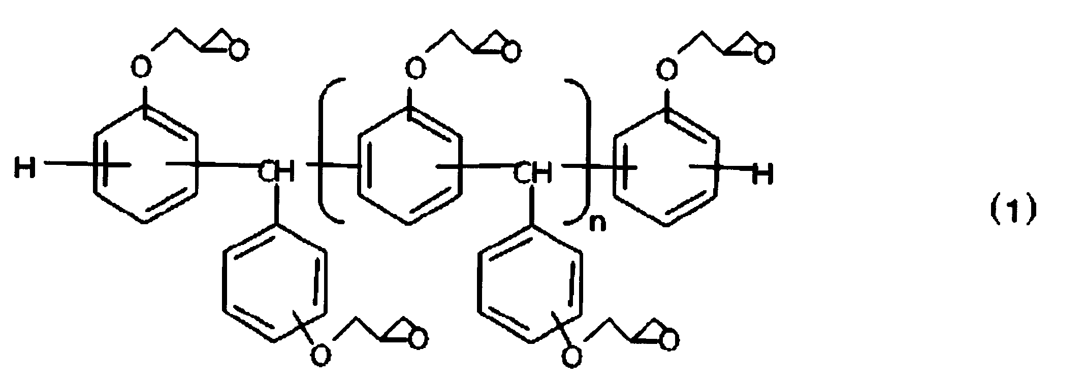
4.30質量部
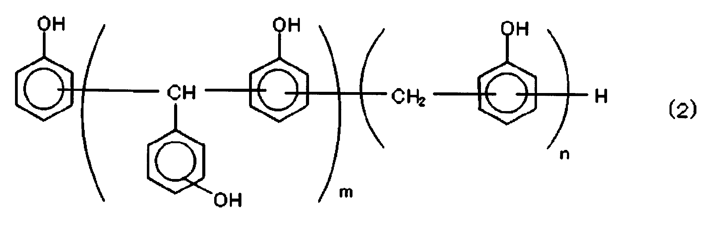
溶融球状シリカ2:(平均粒径0.5μm、比表面積5.9m2/g) 15質量部
硬化促進剤1:トリフェニルホスフィン(ケイ・アイ化成(株)製、商品名PP-360)
0.1質量部
着色剤:カーボンブラック(比表面積29m2/g、DBP吸収量71cm3/100g)
0.3質量部
カップリング剤:N-フェニルγ-アミノプロピルトリメトキシシラン(信越化学(株)製、商品名KBM-573)
0.2質量部
離型剤:モンタン酸エステル系ワックス(クラリアントジャパン(株)製、商品名リコルブWE-4)
0.15質量部
上記配合の樹脂組成物の原材料をスーパーミキサーにより5分間粉砕混合したのち、この混合原料を準備した。
図6に示す円筒状外周部302の素材として孔径2.5mmの小孔を有している鉄製の打ち抜き金網を使用した。直径20cmの回転子301の外周上に円筒状に加工した高さ25mm、厚さ1.5mmの打ち抜き金網を取り付け、円筒状外周部302を形成した。回転子301を3000RPMで回転させ、円筒状外周部302を励磁コイルで115℃に加熱した。回転子301の回転数と、円筒状外周部302の温度が定常状態になった後、脱気装置により脱気しつつ二軸押出機309により上記マスターバッチを溶融混練して得られた溶融物を、回転子301の上方より2重管式円筒体305を通して2kg/hrの割合で回転子301の内側に供給した。これにより、回転子301を回転させて得られる遠心力によって円筒状外周部302の複数の小孔に溶融物を通過させることで、顆粒状の半導体封止用樹脂組成物を得た。
マウントフィルム(日東電工(株)製:リバアルファ(登録商標))上に、複数の半導体素子を並べて配置した。続いて、上記顆粒状の半導体封止用樹脂組成物を用いて圧縮成形を行い、マウントフィルム上の半導体素子を封止した。圧縮成形の条件としては、成形温度125℃、硬化時間7分であった。この後、ポストキュアを150℃、1時間で行った後、マウントフィルムを剥離し、更にポストキュアを175℃、4時間で行った。
表1の配合に従い、実施例1と同様にして顆粒状の樹脂組成物を製造したのち、実施例1と同様にして半導体装置を製造した。
実施例1以外で用いた原材料を以下に示す。
エポキシ樹脂2:下記式(3)で表されるビフェニレン骨格を有するフェノールアラルキル型エポキシ樹脂(日本化薬(株)製、商品名NC3000P、軟化点58℃、エポキシ当量273)

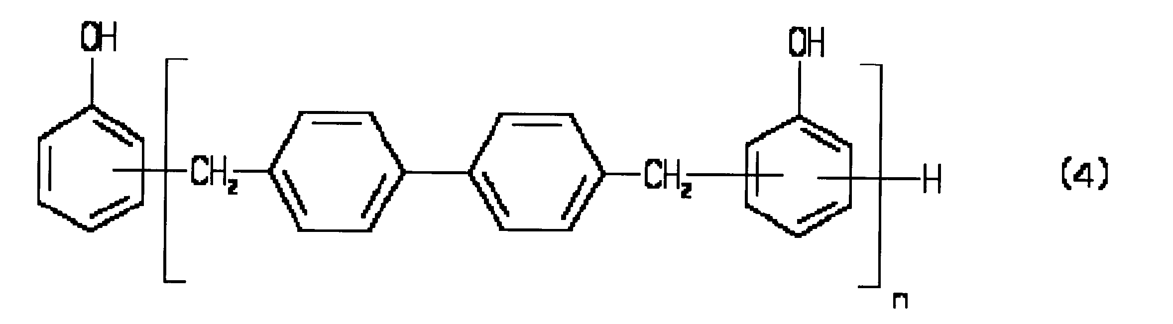
硬化促進剤3:テトラフェニルホスホニウム・ビス(ナフタレン-2,3-ジオキシ)フェニルシリケート(住友ベークライト(株)製)
硬化促進剤4:テトラフェニルホスホニウム・4,4'-スルフォニルジフェノラート(住友ベークライト(株)製)
硬化促進剤5:テトラフェニルホスホニウム・2,3'-ジヒドロキシナフタレート(住友ベークライト(株)製)
硬化促進剤6:下記式(5)で表される2-(トリフェニルホスホニウム)フェノラート


各評価については、下記の条件に従って行った。
・イオン粘度
誘電分析装置本体としてNETZSCH社製のDEA231/1 cure analyzerを使用し、プレスとしてNETZSCH社製のMP235 Mini-Pressを使用して、ASTM E2039に準拠して、測定温度125℃、測定周波数100Hzの条件にて、実施例および比較例で得られた顆粒状の樹脂組成物を粉末状にした試料約3gをプレス内の電極部上面に導入した後、プレスして測定した。得られた粘度プロファイルから、最低イオン粘度、600秒経過後のイオン粘度、及び飽和イオン粘度に達した時間を求めた。最低イオン粘度、600秒経過後のイオン粘度の単位は無し、飽和イオン粘度に達した時間の単位は秒(sec.)。測定結果を表2に示す。
実施例および比較例で得られた顆粒状の樹脂組成物について、高化式フローテスター((株)島津製作所・製CFT-500)を用いて、125℃、圧力40kgf/cm2、キャピラリー径0.5mmの条件で高化式粘度を測定した。単位はPa・s。測定結果を表2に示す。
実施例および比較例で得られた顆粒状の樹脂組成物を用いてトランスファー成形を行い、長さ800mm、幅10mm、厚さ4mmの試験片を成形した。トランスファー成形の条件は、成形温度125℃、硬化時間10分とした。成形時、型開き10秒後、ショアD硬度計を用いて試験片のショアD硬度を測定した。測定結果を表2に示す。
実施例および比較例で得られた顆粒状の樹脂組成物を用いてトランスファー成形を行い、JIS曲げ試験片を得た。トランスファー成形の条件は、成形温度125℃、硬化時間7分とした。得られた試験片の260℃における曲げ強度および曲げ弾性率を、JIS K 6911に準じて測定した。単位はMPa。測定結果を表2に示す。
実施例および比較例で得られた顆粒状の樹脂組成物を用いてトランスファー成形を行い、長さ15mm、幅4mm、厚さ3mmの試験片を得た。トランスファー成形の条件は、成形温度125℃、硬化時間7分とした。得られた試験片を、熱膨張計(セイコーインスツルメント社製TMA-120)を用い、室温(25℃)から5℃/分の昇温速度で昇温して、試験片の伸び率が急激に変化する温度をガラス転移温度として求めた。単位は℃である。また、室温(25℃)からTg-30℃の間での平均の線膨張係数を求め、α1とした。単位はppm/℃。測定結果を表2に示す。
実施例および比較例で得られた顆粒状の樹脂組成物を用いてトランスファー成形を行い、幅4mm、長さ20mm、厚み0.1mmの試験片を得た。トランスファー成形の条件は、成形温度125℃、硬化時間7分とした。得られた試験片を、三点曲げモード、周波数10Hz、測定温度260℃の条件で、DMA(Dynamic mechanical analysis/動的粘弾性測定器)を用いて測定した際の、260℃における貯蔵弾性率(E')を求めた。単位はMPa。測定結果を表2に示す。
実施例および比較例の半導体装置の製造工程において、マウントフィルムを剥離する際に、測定温度180℃、引き剥がし速度50mm/minの条件で、封止材層とマウントフィルムとを引き剥がし、ピール強度を求めた。単位はN/m。測定結果を表2に示す。
実施例および比較例の半導体装置の製造工程において、マウントを剥離した後の封止材層下面とホルムアミドとの接触角を、Dropmaster500(協和科学(株)製)を用いて、25℃において液滴を静置し、10秒後の値を計測することを3回繰り返し、その平均値を取った。単位は°(度)。結果を表2に示す。
実施例および比較例の半導体装置の製造工程において、マウントフィルムを剥離した後の封止材層下面と再配線材料(住友ベークライト(株)製、CRC-8902)との接触角を、Dropmaster500(協和科学(株)製)を用いて、25℃において液滴を静置し、10秒後の値を計測することを3回繰り返し、その平均値を取った。単位は°(度)。結果を表2に示す。
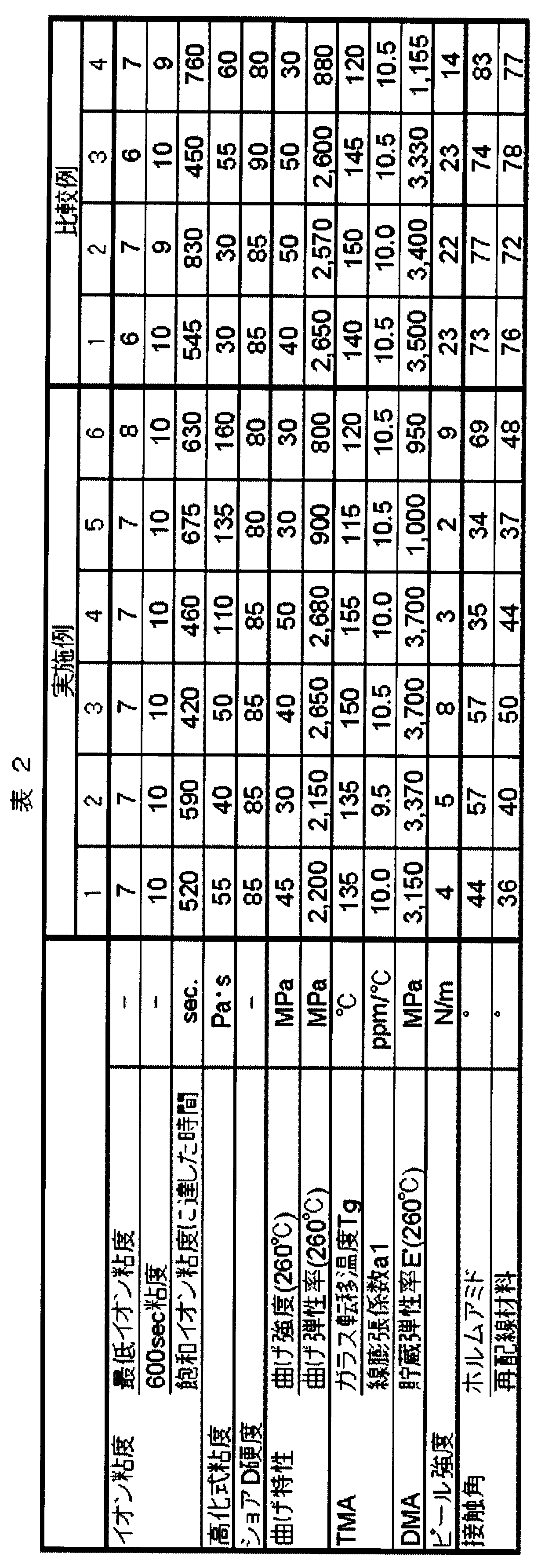
20 下面
30 下面
100 半導体装置
102 キャリア
104 マウントフィルム
106 半導体素子
108 封止材層
110 再配線用絶縁樹脂層
112 開口部
114 ビア
116 再配線回路
118 ソルダーレジスト層
120 半田ボール
122 パッド
200 再配線用疑似ウエハ
210 ウエハレベルパッケージ
301 回転子
302 円筒状外周部
303 磁性材料
304 励磁コイル
305 2重管式円筒体
306 交流電源発生装置
307 冷却ジャケット
308 外槽
309 二軸押出機
310 モーター
Claims (14)
- 熱剥離性粘着層の主面上に、複数の半導体素子を配置する工程と、
半導体封止用樹脂組成物を用いて、前記熱剥離性粘着層の前記主面上の複数の前記半導体素子を封止する封止材層を形成する工程と、
前記熱剥離性粘着層を剥離することにより、前記封止材層の下面および前記半導体素子の下面を露出させる工程と、を含み、
前記熱剥離性粘着層を剥離する前記工程の後における、前記封止材層の前記下面の接触角が、ホルムアミドを用いた測定時において、70度以下である、半導体装置の製造方法。 - 前記封止材層を形成する工程は、100℃以上150℃以下の温度条件で硬化処理を行う工程を含む、請求項1に記載の半導体装置の製造方法。
- 前記熱剥離性粘着層を剥離する前記工程の後、前記封止材層の前記下面上および前記半導体素子の前記下面上に、再配線用絶縁樹脂層を形成する工程と、
前記再配線用絶縁樹脂層上に、再配線回路を形成する工程と、を含む、請求項1または2に記載の半導体装置の製造方法。 - 前記熱剥離性粘着層を剥離する前記工程の後、前記再配線用絶縁樹脂層を形成する工程の前に、150℃以上200℃以下の温度条件で、更に硬化後処理を行う工程を含む、請求項3に記載の半導体装置の製造方法。
- 前記封止材層を形成する前記工程において、顆粒の前記半導体封止用樹脂組成物を用い、圧縮形成を行うことにより、前記封止材層を形成する、請求項1または2に記載の半導体装置の製造方法。
- 誘電分析装置を用いて、測定温度125℃、測定周波数100Hzの条件で測定した際の、前記半導体封止用樹脂組成物の飽和イオン粘度に到達する時刻が、測定開始から100秒以上、900秒以下にある、請求項1または2に記載の半導体装置の製造方法。
- 測定温度180℃、引き剥がし速度50mm/minの条件で測定した際の、前記封止材層と前記マウントフィルムとのピール強度が1N/m以上、10N/m以下である、請求項1または2に記載の半導体装置の製造方法。
- 125℃、10分の条件で硬化させた後の前記封止材層のショアD硬度が70以上である、請求項1または2に記載の半導体装置の製造方法。
- 誘電分析装置を用いて、測定温度125℃、測定周波数100Hzの条件で測定した際の、前記半導体封止用樹脂組成物の最低イオン粘度が、6以上、8以下であり、かつ、測定開始からの経過時間が600秒後のイオン粘度が、9以上11以下である、請求項1または2に記載の半導体装置の製造方法。
- 高化式粘度測定装置を用いて、測定温度125℃、荷重40kgで測定した際の、前記半導体封止用樹脂組成物の高化式粘度が、20Pa・s以上200Pa・s以下である、請求項1または2に記載の半導体装置の製造方法。
- 260℃における、前記封止材層の曲げ強度が、10MPa以上、100MPa以下である、請求項1または2に記載の半導体装置の製造方法。
- 260℃における、前記封止材層の曲げ弾性率が、5×10²MPa以上、3×10³MPa以下である、請求項1または2に記載の半導体装置の製造方法。
- 動的粘弾性測定器を用い、三点曲げモード、周波数10Hz、測定温度260℃で測定した際の、前記封止材層の貯蔵弾性率(E')が、5×10²MPa以上、5×10³MPa以下である、請求項1または2に記載の半導体装置の製造方法。
- 請求項1または2に記載の半導体装置の製造方法で得られた、半導体装置。
Priority Applications (5)
| Application Number | Priority Date | Filing Date | Title |
|---|---|---|---|
| KR1020137024478A KR101872556B1 (ko) | 2011-03-10 | 2012-03-09 | 반도체 장치 및 반도체 장치의 제조 방법 |
| SG2013068507A SG193419A1 (en) | 2011-03-10 | 2012-03-09 | Semiconductor device, and process for manufacturing semiconductor device |
| CN201280012160.7A CN103415923B (zh) | 2011-03-10 | 2012-03-09 | 半导体装置和半导体装置的制造方法 |
| US14/003,404 US20130337608A1 (en) | 2011-03-10 | 2012-03-09 | Semiconductor device, and process for manufacturing semiconductor device |
| JP2013503625A JP6032197B2 (ja) | 2011-03-10 | 2012-03-09 | 半導体装置の製造方法 |
Applications Claiming Priority (2)
| Application Number | Priority Date | Filing Date | Title |
|---|---|---|---|
| JP2011053541 | 2011-03-10 | ||
| JP2011-053541 | 2011-03-10 |
Publications (1)
| Publication Number | Publication Date |
|---|---|
| WO2012121377A1 true WO2012121377A1 (ja) | 2012-09-13 |
Family
ID=46798328
Family Applications (1)
| Application Number | Title | Priority Date | Filing Date |
|---|---|---|---|
| PCT/JP2012/056140 Ceased WO2012121377A1 (ja) | 2011-03-10 | 2012-03-09 | 半導体装置および半導体装置の製造方法 |
Country Status (7)
| Country | Link |
|---|---|
| US (1) | US20130337608A1 (ja) |
| JP (1) | JP6032197B2 (ja) |
| KR (1) | KR101872556B1 (ja) |
| CN (1) | CN103415923B (ja) |
| SG (1) | SG193419A1 (ja) |
| TW (1) | TWI590394B (ja) |
| WO (1) | WO2012121377A1 (ja) |
Cited By (7)
| Publication number | Priority date | Publication date | Assignee | Title |
|---|---|---|---|---|
| JP2017088828A (ja) * | 2015-11-17 | 2017-05-25 | 住友ベークライト株式会社 | 半導体封止用樹脂組成物、半導体装置および構造体 |
| JP2017524250A (ja) * | 2014-07-20 | 2017-08-24 | エックス−セレプリント リミテッドX−Celeprint Limited | マイクロ転写印刷のための装置および方法 |
| WO2018220868A1 (ja) * | 2017-05-30 | 2018-12-06 | アオイ電子株式会社 | 半導体装置および半導体装置の製造方法 |
| JP2019024130A (ja) * | 2018-11-14 | 2019-02-14 | アオイ電子株式会社 | 半導体装置の製造方法 |
| US11062936B1 (en) | 2019-12-19 | 2021-07-13 | X Display Company Technology Limited | Transfer stamps with multiple separate pedestals |
| JP2022191847A (ja) * | 2021-06-16 | 2022-12-28 | 住友ベークライト株式会社 | 低温硬化性樹脂組成物、および電子装置 |
| WO2023013732A1 (ja) * | 2021-08-06 | 2023-02-09 | パナソニックIpマネジメント株式会社 | フラックス用樹脂組成物、はんだペースト及び実装構造体 |
Families Citing this family (23)
| Publication number | Priority date | Publication date | Assignee | Title |
|---|---|---|---|---|
| US9161448B2 (en) | 2010-03-29 | 2015-10-13 | Semprius, Inc. | Laser assisted transfer welding process |
| US9412727B2 (en) | 2011-09-20 | 2016-08-09 | Semprius, Inc. | Printing transferable components using microstructured elastomeric surfaces with pressure modulated reversible adhesion |
| DE102013106353B4 (de) * | 2013-06-18 | 2018-06-28 | Tdk Corporation | Verfahren zum Aufbringen einer strukturierten Beschichtung auf ein Bauelement |
| US9324680B2 (en) * | 2013-09-19 | 2016-04-26 | Intel Corporation | Solder attach apparatus and method |
| TWI582866B (zh) * | 2014-04-03 | 2017-05-11 | 矽品精密工業股份有限公司 | 半導體封裝件之製法及其所用之支撐件 |
| KR101676916B1 (ko) * | 2014-08-20 | 2016-11-16 | 앰코 테크놀로지 코리아 주식회사 | 반도체 디바이스의 제조 방법 및 이에 따른 반도체 디바이스 |
| US9666556B2 (en) * | 2015-06-29 | 2017-05-30 | Taiwan Semiconductor Manufacturing Company, Ltd. | Flip chip packaging |
| US9704821B2 (en) | 2015-08-11 | 2017-07-11 | X-Celeprint Limited | Stamp with structured posts |
| US10468363B2 (en) | 2015-08-10 | 2019-11-05 | X-Celeprint Limited | Chiplets with connection posts |
| CN105161431A (zh) * | 2015-08-12 | 2015-12-16 | 中芯长电半导体(江阴)有限公司 | 晶圆级芯片封装方法 |
| US10103069B2 (en) | 2016-04-01 | 2018-10-16 | X-Celeprint Limited | Pressure-activated electrical interconnection by micro-transfer printing |
| EP3460005B1 (en) * | 2016-05-18 | 2022-05-11 | Sumitomo Bakelite Co.Ltd. | Thermosetting resin composition for lds, resin molded article and three-dimensional molded circuit component |
| US10222698B2 (en) | 2016-07-28 | 2019-03-05 | X-Celeprint Limited | Chiplets with wicking posts |
| US11064609B2 (en) | 2016-08-04 | 2021-07-13 | X Display Company Technology Limited | Printable 3D electronic structure |
| CN109643666A (zh) * | 2016-08-24 | 2019-04-16 | 东丽工程株式会社 | 安装方法和安装装置 |
| WO2018057040A1 (en) * | 2016-09-26 | 2018-03-29 | Brown Andrew J | Semiconductor device and method of making |
| JP2019033124A (ja) * | 2017-08-04 | 2019-02-28 | リンテック株式会社 | 半導体装置の製造方法、及び接着積層体 |
| TWI631684B (zh) * | 2017-09-05 | 2018-08-01 | Phoenix Pioneer Technology Co., Ltd. | 中介基板及其製法 |
| US10796971B2 (en) | 2018-08-13 | 2020-10-06 | X Display Company Technology Limited | Pressure-activated electrical interconnection with additive repair |
| CN109638108B (zh) * | 2018-12-05 | 2020-04-14 | 上海空间电源研究所 | 平流层飞行器针对翘曲柔性太阳电池片的组件封装方法 |
| US11495588B2 (en) * | 2018-12-07 | 2022-11-08 | Advanced Micro Devices, Inc. | Circuit board with compact passive component arrangement |
| US10748793B1 (en) | 2019-02-13 | 2020-08-18 | X Display Company Technology Limited | Printing component arrays with different orientations |
| TWI903494B (zh) * | 2024-05-09 | 2025-11-01 | 矽品精密工業股份有限公司 | 電子組件及其製法 |
Citations (6)
| Publication number | Priority date | Publication date | Assignee | Title |
|---|---|---|---|---|
| JPH11130938A (ja) * | 1997-10-29 | 1999-05-18 | Sumitomo Bakelite Co Ltd | エポキシ樹脂組成物及び半導体装置 |
| JP2005005632A (ja) * | 2003-06-16 | 2005-01-06 | Sony Corp | チップ状電子部品及びその製造方法、並びにその実装構造 |
| JP2006335835A (ja) * | 2005-05-31 | 2006-12-14 | Sumitomo Bakelite Co Ltd | エポキシ樹脂組成物および半導体装置 |
| JP2008081683A (ja) * | 2006-09-28 | 2008-04-10 | Sumitomo Bakelite Co Ltd | エポキシ樹脂組成物、半導体封止用エポキシ樹脂組成物および半導体装置 |
| JP2010070622A (ja) * | 2008-09-18 | 2010-04-02 | Sumitomo Bakelite Co Ltd | エポキシ樹脂組成物、半導体封止用エポキシ樹脂組成物及び半導体装置 |
| JP2010165940A (ja) * | 2009-01-16 | 2010-07-29 | Shinko Electric Ind Co Ltd | 半導体素子の樹脂封止方法 |
Family Cites Families (7)
| Publication number | Priority date | Publication date | Assignee | Title |
|---|---|---|---|---|
| JP2970569B2 (ja) * | 1997-01-13 | 1999-11-02 | 日本電気株式会社 | 樹脂封止方法および樹脂封止金型装置 |
| TWI281924B (en) * | 2003-04-07 | 2007-06-01 | Hitachi Chemical Co Ltd | Epoxy resin molding material for sealing use and semiconductor device |
| JPWO2005007756A1 (ja) * | 2003-05-21 | 2006-08-31 | 日立化成工業株式会社 | プライマ、樹脂付き導体箔、積層板並びに積層板の製造方法 |
| CN101160026B (zh) * | 2003-05-21 | 2011-08-03 | 日立化成工业株式会社 | 底漆、带有树脂的导体箔、层叠板以及层叠板的制造方法 |
| US7326592B2 (en) | 2005-04-04 | 2008-02-05 | Infineon Technologies Ag | Stacked die package |
| JP2008144047A (ja) * | 2006-12-11 | 2008-06-26 | Three M Innovative Properties Co | 耐熱性マスキングテープ及びその使用方法 |
| MY152389A (en) * | 2008-12-10 | 2014-09-15 | Sumitomo Bakelite Co | Resin composition for encapsulating semiconductor, method for producing semiconductor device and semiconductor device |
-
2012
- 2012-03-09 CN CN201280012160.7A patent/CN103415923B/zh not_active Expired - Fee Related
- 2012-03-09 KR KR1020137024478A patent/KR101872556B1/ko not_active Expired - Fee Related
- 2012-03-09 SG SG2013068507A patent/SG193419A1/en unknown
- 2012-03-09 WO PCT/JP2012/056140 patent/WO2012121377A1/ja not_active Ceased
- 2012-03-09 JP JP2013503625A patent/JP6032197B2/ja not_active Expired - Fee Related
- 2012-03-09 US US14/003,404 patent/US20130337608A1/en not_active Abandoned
- 2012-03-09 TW TW101108144A patent/TWI590394B/zh not_active IP Right Cessation
Patent Citations (6)
| Publication number | Priority date | Publication date | Assignee | Title |
|---|---|---|---|---|
| JPH11130938A (ja) * | 1997-10-29 | 1999-05-18 | Sumitomo Bakelite Co Ltd | エポキシ樹脂組成物及び半導体装置 |
| JP2005005632A (ja) * | 2003-06-16 | 2005-01-06 | Sony Corp | チップ状電子部品及びその製造方法、並びにその実装構造 |
| JP2006335835A (ja) * | 2005-05-31 | 2006-12-14 | Sumitomo Bakelite Co Ltd | エポキシ樹脂組成物および半導体装置 |
| JP2008081683A (ja) * | 2006-09-28 | 2008-04-10 | Sumitomo Bakelite Co Ltd | エポキシ樹脂組成物、半導体封止用エポキシ樹脂組成物および半導体装置 |
| JP2010070622A (ja) * | 2008-09-18 | 2010-04-02 | Sumitomo Bakelite Co Ltd | エポキシ樹脂組成物、半導体封止用エポキシ樹脂組成物及び半導体装置 |
| JP2010165940A (ja) * | 2009-01-16 | 2010-07-29 | Shinko Electric Ind Co Ltd | 半導体素子の樹脂封止方法 |
Cited By (10)
| Publication number | Priority date | Publication date | Assignee | Title |
|---|---|---|---|---|
| JP2017524250A (ja) * | 2014-07-20 | 2017-08-24 | エックス−セレプリント リミテッドX−Celeprint Limited | マイクロ転写印刷のための装置および方法 |
| JP2017088828A (ja) * | 2015-11-17 | 2017-05-25 | 住友ベークライト株式会社 | 半導体封止用樹脂組成物、半導体装置および構造体 |
| WO2018220868A1 (ja) * | 2017-05-30 | 2018-12-06 | アオイ電子株式会社 | 半導体装置および半導体装置の製造方法 |
| JP2018206797A (ja) * | 2017-05-30 | 2018-12-27 | アオイ電子株式会社 | 半導体装置および半導体装置の製造方法 |
| CN110709970A (zh) * | 2017-05-30 | 2020-01-17 | 青井电子株式会社 | 半导体装置及半导体装置的制造方法 |
| US11075180B2 (en) | 2017-05-30 | 2021-07-27 | Aoi Electronics Co., Ltd. | Semiconductor device and method of manufacturing the semiconductor device |
| JP2019024130A (ja) * | 2018-11-14 | 2019-02-14 | アオイ電子株式会社 | 半導体装置の製造方法 |
| US11062936B1 (en) | 2019-12-19 | 2021-07-13 | X Display Company Technology Limited | Transfer stamps with multiple separate pedestals |
| JP2022191847A (ja) * | 2021-06-16 | 2022-12-28 | 住友ベークライト株式会社 | 低温硬化性樹脂組成物、および電子装置 |
| WO2023013732A1 (ja) * | 2021-08-06 | 2023-02-09 | パナソニックIpマネジメント株式会社 | フラックス用樹脂組成物、はんだペースト及び実装構造体 |
Also Published As
| Publication number | Publication date |
|---|---|
| CN103415923B (zh) | 2016-06-08 |
| JPWO2012121377A1 (ja) | 2014-07-17 |
| CN103415923A (zh) | 2013-11-27 |
| JP6032197B2 (ja) | 2016-11-24 |
| KR20140012672A (ko) | 2014-02-03 |
| SG193419A1 (en) | 2013-11-29 |
| KR101872556B1 (ko) | 2018-06-28 |
| US20130337608A1 (en) | 2013-12-19 |
| TWI590394B (zh) | 2017-07-01 |
| TW201240032A (en) | 2012-10-01 |
Similar Documents
| Publication | Publication Date | Title |
|---|---|---|
| JP6032197B2 (ja) | 半導体装置の製造方法 | |
| KR101712216B1 (ko) | 반도체 봉지용 수지 조성물, 반도체 장치의 제조 방법 및 반도체 장치 | |
| JP7078138B2 (ja) | 半導体装置の製造方法 | |
| JP5799532B2 (ja) | 半導体封止用樹脂組成物、半導体装置および半導体装置の製造方法 | |
| JP6766360B2 (ja) | 樹脂組成物 | |
| JP2012052089A (ja) | 機能性粒子、充填剤、電子部品用樹脂組成物、電子部品および半導体装置 | |
| JP2021120462A (ja) | 熱硬化性樹脂組成物、樹脂封止基板、および電子装置 | |
| CN105968324B (zh) | 密封用树脂组合物、电子零件的制造方法和电子零件 | |
| JP2024166236A (ja) | 熱硬化性樹脂組成物、及び電子装置 | |
| JP2019026715A (ja) | 一括封止用エポキシ樹脂組成物、電子装置およびその製造方法 | |
| JP2020123670A (ja) | 半導体パッケージおよびそれに用いる封止用エポキシ樹脂組成物 | |
| JP2021113267A (ja) | 熱硬化性樹脂組成物、電子装置、熱伝導性材料の製造方法、熱硬化性樹脂組成物の製造方法 | |
| JP2017088828A (ja) | 半導体封止用樹脂組成物、半導体装置および構造体 | |
| JP7501105B2 (ja) | 樹脂被覆無機粒子、熱硬化性樹脂組成物、半導体装置、樹脂被覆無機粒子の製造方法 | |
| JP2018024770A (ja) | 封止用樹脂組成物、および半導体装置 | |
| JP2021113270A (ja) | 樹脂組成物、樹脂組成物の製造方法、及び、これらに用いる無機粒子 | |
| JP5167587B2 (ja) | 半導体封止用エポキシ樹脂組成物及び半導体装置 | |
| JP6776597B2 (ja) | 熱硬化性樹脂組成物、樹脂封止基板、および電子装置 | |
| JP2021113269A (ja) | 熱硬化性樹脂組成物、電子装置、及び熱硬化性樹脂組成物の製造方法 | |
| JP2016023279A (ja) | 封止用樹脂組成物、半導体装置および構造体 | |
| KR102352497B1 (ko) | 열경화성 수지 조성물, 수지 봉지 기판, 및 전자 장치 | |
| WO2021205892A1 (ja) | 半導体封止用樹脂成形材の製造方法、半導体パッケージの製造方法、及び半導体装置の製造方法 | |
| JP2020132723A (ja) | 半導体封止用樹脂組成物および半導体装置 | |
| CN107429041A (zh) | 压缩成型用模具底部填充材料、半导体封装、结构体和半导体封装的制造方法 | |
| JP2015218294A (ja) | 封止用樹脂組成物の製造方法、および半導体装置の製造方法 |
Legal Events
| Date | Code | Title | Description |
|---|---|---|---|
| 121 | Ep: the epo has been informed by wipo that ep was designated in this application |
Ref document number: 12755678 Country of ref document: EP Kind code of ref document: A1 |
|
| ENP | Entry into the national phase |
Ref document number: 2013503625 Country of ref document: JP Kind code of ref document: A |
|
| WWE | Wipo information: entry into national phase |
Ref document number: 14003404 Country of ref document: US |
|
| NENP | Non-entry into the national phase |
Ref country code: DE |
|
| WWE | Wipo information: entry into national phase |
Ref document number: 1301005003 Country of ref document: TH |
|
| ENP | Entry into the national phase |
Ref document number: 20137024478 Country of ref document: KR Kind code of ref document: A |
|
| 122 | Ep: pct application non-entry in european phase |
Ref document number: 12755678 Country of ref document: EP Kind code of ref document: A1 |