WO2012118028A1 - 色素増感太陽電池モジュール - Google Patents
色素増感太陽電池モジュール Download PDFInfo
- Publication number
- WO2012118028A1 WO2012118028A1 PCT/JP2012/054815 JP2012054815W WO2012118028A1 WO 2012118028 A1 WO2012118028 A1 WO 2012118028A1 JP 2012054815 W JP2012054815 W JP 2012054815W WO 2012118028 A1 WO2012118028 A1 WO 2012118028A1
- Authority
- WO
- WIPO (PCT)
- Prior art keywords
- dye
- sensitized solar
- solar cell
- electrode
- sealing portion
- Prior art date
Links
- 238000007789 sealing Methods 0.000 claims abstract description 356
- 239000000758 substrate Substances 0.000 claims abstract description 77
- 239000004065 semiconductor Substances 0.000 claims abstract description 33
- 239000010410 layer Substances 0.000 claims description 83
- 239000004020 conductor Substances 0.000 claims description 51
- 239000011241 protective layer Substances 0.000 claims description 40
- 238000002844 melting Methods 0.000 claims description 36
- 239000011810 insulating material Substances 0.000 claims description 35
- 229910052751 metal Inorganic materials 0.000 claims description 35
- 239000002184 metal Substances 0.000 claims description 35
- 239000000463 material Substances 0.000 claims description 33
- 230000008018 melting Effects 0.000 claims description 33
- 229920005989 resin Polymers 0.000 claims description 26
- 239000011347 resin Substances 0.000 claims description 26
- 239000003792 electrolyte Substances 0.000 claims description 22
- 206010070834 Sensitisation Diseases 0.000 claims description 5
- 230000008313 sensitization Effects 0.000 claims description 5
- 238000000113 differential scanning calorimetry Methods 0.000 description 41
- 238000005192 partition Methods 0.000 description 29
- 239000000975 dye Substances 0.000 description 22
- 230000015572 biosynthetic process Effects 0.000 description 14
- 238000004519 manufacturing process Methods 0.000 description 13
- 239000003504 photosensitizing agent Substances 0.000 description 13
- 230000002165 photosensitisation Effects 0.000 description 12
- 230000000052 comparative effect Effects 0.000 description 11
- 239000012298 atmosphere Substances 0.000 description 10
- 238000010248 power generation Methods 0.000 description 10
- 239000011521 glass Substances 0.000 description 9
- -1 polyethylene terephthalate Polymers 0.000 description 9
- 238000000034 method Methods 0.000 description 8
- BASFCYQUMIYNBI-UHFFFAOYSA-N platinum Chemical compound [Pt] BASFCYQUMIYNBI-UHFFFAOYSA-N 0.000 description 8
- BQCADISMDOOEFD-UHFFFAOYSA-N Silver Chemical compound [Ag] BQCADISMDOOEFD-UHFFFAOYSA-N 0.000 description 7
- 238000005520 cutting process Methods 0.000 description 7
- 238000010438 heat treatment Methods 0.000 description 7
- 230000007257 malfunction Effects 0.000 description 7
- 238000000059 patterning Methods 0.000 description 7
- 229910052709 silver Inorganic materials 0.000 description 7
- 239000004332 silver Substances 0.000 description 7
- WEVYAHXRMPXWCK-UHFFFAOYSA-N Acetonitrile Chemical compound CC#N WEVYAHXRMPXWCK-UHFFFAOYSA-N 0.000 description 6
- 239000004743 Polypropylene Substances 0.000 description 6
- GWEVSGVZZGPLCZ-UHFFFAOYSA-N Titan oxide Chemical compound O=[Ti]=O GWEVSGVZZGPLCZ-UHFFFAOYSA-N 0.000 description 6
- WFDIJRYMOXRFFG-UHFFFAOYSA-N acetic acid anhydride Natural products CC(=O)OC(C)=O WFDIJRYMOXRFFG-UHFFFAOYSA-N 0.000 description 6
- 238000001035 drying Methods 0.000 description 6
- 239000000853 adhesive Substances 0.000 description 5
- 230000001070 adhesive effect Effects 0.000 description 5
- 239000003054 catalyst Substances 0.000 description 5
- 238000010304 firing Methods 0.000 description 5
- 239000002245 particle Substances 0.000 description 5
- 239000004642 Polyimide Substances 0.000 description 4
- 229920005648 ethylene methacrylic acid copolymer Polymers 0.000 description 4
- 230000002093 peripheral effect Effects 0.000 description 4
- 229910052697 platinum Inorganic materials 0.000 description 4
- 229920001721 polyimide Polymers 0.000 description 4
- 229920001155 polypropylene Polymers 0.000 description 4
- 238000003825 pressing Methods 0.000 description 4
- 238000007650 screen-printing Methods 0.000 description 4
- 239000002904 solvent Substances 0.000 description 4
- 229910001887 tin oxide Inorganic materials 0.000 description 4
- 229920000219 Ethylene vinyl alcohol Polymers 0.000 description 3
- 239000004698 Polyethylene Substances 0.000 description 3
- RTAQQCXQSZGOHL-UHFFFAOYSA-N Titanium Chemical compound [Ti] RTAQQCXQSZGOHL-UHFFFAOYSA-N 0.000 description 3
- 238000006243 chemical reaction Methods 0.000 description 3
- 229920001577 copolymer Polymers 0.000 description 3
- 239000002608 ionic liquid Substances 0.000 description 3
- 229920000554 ionomer Polymers 0.000 description 3
- 239000007769 metal material Substances 0.000 description 3
- 239000003960 organic solvent Substances 0.000 description 3
- 230000035515 penetration Effects 0.000 description 3
- 229920000573 polyethylene Polymers 0.000 description 3
- 229920002451 polyvinyl alcohol Polymers 0.000 description 3
- 238000000926 separation method Methods 0.000 description 3
- 238000004544 sputter deposition Methods 0.000 description 3
- 239000000126 substance Substances 0.000 description 3
- XOLBLPGZBRYERU-UHFFFAOYSA-N tin dioxide Chemical compound O=[Sn]=O XOLBLPGZBRYERU-UHFFFAOYSA-N 0.000 description 3
- 229920002554 vinyl polymer Polymers 0.000 description 3
- XLYOFNOQVPJJNP-UHFFFAOYSA-N water Substances O XLYOFNOQVPJJNP-UHFFFAOYSA-N 0.000 description 3
- YEJRWHAVMIAJKC-UHFFFAOYSA-N 4-Butyrolactone Chemical compound O=C1CCCO1 YEJRWHAVMIAJKC-UHFFFAOYSA-N 0.000 description 2
- PXHVJJICTQNCMI-UHFFFAOYSA-N Nickel Chemical compound [Ni] PXHVJJICTQNCMI-UHFFFAOYSA-N 0.000 description 2
- 239000004793 Polystyrene Substances 0.000 description 2
- VYPSYNLAJGMNEJ-UHFFFAOYSA-N Silicium dioxide Chemical compound O=[Si]=O VYPSYNLAJGMNEJ-UHFFFAOYSA-N 0.000 description 2
- 229910006404 SnO 2 Inorganic materials 0.000 description 2
- DKGAVHZHDRPRBM-UHFFFAOYSA-N Tert-Butanol Chemical compound CC(C)(C)O DKGAVHZHDRPRBM-UHFFFAOYSA-N 0.000 description 2
- 239000003575 carbonaceous material Substances 0.000 description 2
- 239000000470 constituent Substances 0.000 description 2
- 125000004122 cyclic group Chemical group 0.000 description 2
- 230000006866 deterioration Effects 0.000 description 2
- 238000009792 diffusion process Methods 0.000 description 2
- 229910003437 indium oxide Inorganic materials 0.000 description 2
- PJXISJQVUVHSOJ-UHFFFAOYSA-N indium(iii) oxide Chemical compound [O-2].[O-2].[O-2].[In+3].[In+3] PJXISJQVUVHSOJ-UHFFFAOYSA-N 0.000 description 2
- 238000003475 lamination Methods 0.000 description 2
- 238000013035 low temperature curing Methods 0.000 description 2
- 229910044991 metal oxide Inorganic materials 0.000 description 2
- 150000004706 metal oxides Chemical class 0.000 description 2
- 229920000139 polyethylene terephthalate Polymers 0.000 description 2
- 239000005020 polyethylene terephthalate Substances 0.000 description 2
- 229920002223 polystyrene Polymers 0.000 description 2
- 238000007639 printing Methods 0.000 description 2
- 150000003839 salts Chemical class 0.000 description 2
- 239000002356 single layer Substances 0.000 description 2
- 238000005118 spray pyrolysis Methods 0.000 description 2
- 239000012780 transparent material Substances 0.000 description 2
- FGYADSCZTQOAFK-UHFFFAOYSA-N 1-methylbenzimidazole Chemical compound C1=CC=C2N(C)C=NC2=C1 FGYADSCZTQOAFK-UHFFFAOYSA-N 0.000 description 1
- JFJNVIPVOCESGZ-UHFFFAOYSA-N 2,3-dipyridin-2-ylpyridine Chemical group N1=CC=CC=C1C1=CC=CN=C1C1=CC=CC=N1 JFJNVIPVOCESGZ-UHFFFAOYSA-N 0.000 description 1
- QKPVEISEHYYHRH-UHFFFAOYSA-N 2-methoxyacetonitrile Chemical compound COCC#N QKPVEISEHYYHRH-UHFFFAOYSA-N 0.000 description 1
- SFPQDYSOPQHZAQ-UHFFFAOYSA-N 2-methoxypropanenitrile Chemical compound COC(C)C#N SFPQDYSOPQHZAQ-UHFFFAOYSA-N 0.000 description 1
- YSHMQTRICHYLGF-UHFFFAOYSA-N 4-tert-butylpyridine Chemical compound CC(C)(C)C1=CC=NC=C1 YSHMQTRICHYLGF-UHFFFAOYSA-N 0.000 description 1
- ZCYVEMRRCGMTRW-UHFFFAOYSA-N 7553-56-2 Chemical compound [I] ZCYVEMRRCGMTRW-UHFFFAOYSA-N 0.000 description 1
- 229910018072 Al 2 O 3 Inorganic materials 0.000 description 1
- 229910015902 Bi 2 O 3 Inorganic materials 0.000 description 1
- ROFVEXUMMXZLPA-UHFFFAOYSA-N Bipyridyl Chemical group N1=CC=CC=C1C1=CC=CC=N1 ROFVEXUMMXZLPA-UHFFFAOYSA-N 0.000 description 1
- CPELXLSAUQHCOX-UHFFFAOYSA-M Bromide Chemical compound [Br-] CPELXLSAUQHCOX-UHFFFAOYSA-M 0.000 description 1
- WKBOTKDWSSQWDR-UHFFFAOYSA-N Bromine atom Chemical compound [Br] WKBOTKDWSSQWDR-UHFFFAOYSA-N 0.000 description 1
- OKTJSMMVPCPJKN-UHFFFAOYSA-N Carbon Chemical compound [C] OKTJSMMVPCPJKN-UHFFFAOYSA-N 0.000 description 1
- RYGMFSIKBFXOCR-UHFFFAOYSA-N Copper Chemical compound [Cu] RYGMFSIKBFXOCR-UHFFFAOYSA-N 0.000 description 1
- OIFBSDVPJOWBCH-UHFFFAOYSA-N Diethyl carbonate Chemical compound CCOC(=O)OCC OIFBSDVPJOWBCH-UHFFFAOYSA-N 0.000 description 1
- KMTRUDSVKNLOMY-UHFFFAOYSA-N Ethylene carbonate Chemical compound O=C1OCCO1 KMTRUDSVKNLOMY-UHFFFAOYSA-N 0.000 description 1
- ZOKXTWBITQBERF-UHFFFAOYSA-N Molybdenum Chemical compound [Mo] ZOKXTWBITQBERF-UHFFFAOYSA-N 0.000 description 1
- 229920003298 Nucrel® Polymers 0.000 description 1
- 229920012266 Poly(ether sulfone) PES Polymers 0.000 description 1
- 239000002202 Polyethylene glycol Substances 0.000 description 1
- JUJWROOIHBZHMG-UHFFFAOYSA-N Pyridine Chemical class C1=CC=NC=C1 JUJWROOIHBZHMG-UHFFFAOYSA-N 0.000 description 1
- 239000012327 Ruthenium complex Substances 0.000 description 1
- 229910004298 SiO 2 Inorganic materials 0.000 description 1
- XLOMVQKBTHCTTD-UHFFFAOYSA-N Zinc monoxide Chemical compound [Zn]=O XLOMVQKBTHCTTD-UHFFFAOYSA-N 0.000 description 1
- 230000002411 adverse Effects 0.000 description 1
- WUOACPNHFRMFPN-UHFFFAOYSA-N alpha-terpineol Chemical compound CC1=CCC(C(C)(C)O)CC1 WUOACPNHFRMFPN-UHFFFAOYSA-N 0.000 description 1
- 229910052782 aluminium Inorganic materials 0.000 description 1
- XAGFODPZIPBFFR-UHFFFAOYSA-N aluminium Chemical compound [Al] XAGFODPZIPBFFR-UHFFFAOYSA-N 0.000 description 1
- 238000007611 bar coating method Methods 0.000 description 1
- LRESCJAINPKJTO-UHFFFAOYSA-N bis(trifluoromethylsulfonyl)azanide;1-ethyl-3-methylimidazol-3-ium Chemical compound CCN1C=C[N+](C)=C1.FC(F)(F)S(=O)(=O)[N-]S(=O)(=O)C(F)(F)F LRESCJAINPKJTO-UHFFFAOYSA-N 0.000 description 1
- 229910000416 bismuth oxide Inorganic materials 0.000 description 1
- 239000005388 borosilicate glass Substances 0.000 description 1
- 229940006460 bromide ion Drugs 0.000 description 1
- GDTBXPJZTBHREO-UHFFFAOYSA-N bromine Substances BrBr GDTBXPJZTBHREO-UHFFFAOYSA-N 0.000 description 1
- 229910052794 bromium Inorganic materials 0.000 description 1
- 239000002041 carbon nanotube Substances 0.000 description 1
- 229910021393 carbon nanotube Inorganic materials 0.000 description 1
- 238000006555 catalytic reaction Methods 0.000 description 1
- 229910000420 cerium oxide Inorganic materials 0.000 description 1
- 238000005229 chemical vapour deposition Methods 0.000 description 1
- 229920001940 conductive polymer Polymers 0.000 description 1
- 229910052802 copper Inorganic materials 0.000 description 1
- 239000010949 copper Substances 0.000 description 1
- 230000007797 corrosion Effects 0.000 description 1
- 238000005260 corrosion Methods 0.000 description 1
- SQIFACVGCPWBQZ-UHFFFAOYSA-N delta-terpineol Natural products CC(C)(O)C1CCC(=C)CC1 SQIFACVGCPWBQZ-UHFFFAOYSA-N 0.000 description 1
- 238000011161 development Methods 0.000 description 1
- 230000018109 developmental process Effects 0.000 description 1
- TYIXMATWDRGMPF-UHFFFAOYSA-N dibismuth;oxygen(2-) Chemical compound [O-2].[O-2].[O-2].[Bi+3].[Bi+3] TYIXMATWDRGMPF-UHFFFAOYSA-N 0.000 description 1
- 238000007606 doctor blade method Methods 0.000 description 1
- 230000000694 effects Effects 0.000 description 1
- YQGOJNYOYNNSMM-UHFFFAOYSA-N eosin Chemical compound [Na+].OC(=O)C1=CC=CC=C1C1=C2C=C(Br)C(=O)C(Br)=C2OC2=C(Br)C(O)=C(Br)C=C21 YQGOJNYOYNNSMM-UHFFFAOYSA-N 0.000 description 1
- 239000000835 fiber Substances 0.000 description 1
- 239000005357 flat glass Substances 0.000 description 1
- 239000003349 gelling agent Substances 0.000 description 1
- OWCYYNSBGXMRQN-UHFFFAOYSA-N holmium(3+);oxygen(2-) Chemical compound [O-2].[O-2].[O-2].[Ho+3].[Ho+3] OWCYYNSBGXMRQN-UHFFFAOYSA-N 0.000 description 1
- 150000004693 imidazolium salts Chemical class 0.000 description 1
- 230000001771 impaired effect Effects 0.000 description 1
- AMGQUBHHOARCQH-UHFFFAOYSA-N indium;oxotin Chemical compound [In].[Sn]=O AMGQUBHHOARCQH-UHFFFAOYSA-N 0.000 description 1
- 229910010272 inorganic material Inorganic materials 0.000 description 1
- 239000011147 inorganic material Substances 0.000 description 1
- 230000010354 integration Effects 0.000 description 1
- 230000009545 invasion Effects 0.000 description 1
- 150000002496 iodine Chemical class 0.000 description 1
- 229910052740 iodine Inorganic materials 0.000 description 1
- 239000011630 iodine Substances 0.000 description 1
- 230000001678 irradiating effect Effects 0.000 description 1
- MRELNEQAGSRDBK-UHFFFAOYSA-N lanthanum(3+);oxygen(2-) Chemical compound [O-2].[O-2].[O-2].[La+3].[La+3] MRELNEQAGSRDBK-UHFFFAOYSA-N 0.000 description 1
- 239000003446 ligand Substances 0.000 description 1
- DZVCFNFOPIZQKX-LTHRDKTGSA-M merocyanine Chemical compound [Na+].O=C1N(CCCC)C(=O)N(CCCC)C(=O)C1=C\C=C\C=C/1N(CCCS([O-])(=O)=O)C2=CC=CC=C2O\1 DZVCFNFOPIZQKX-LTHRDKTGSA-M 0.000 description 1
- 239000000203 mixture Substances 0.000 description 1
- 229910052750 molybdenum Inorganic materials 0.000 description 1
- 239000011733 molybdenum Substances 0.000 description 1
- 229910052759 nickel Inorganic materials 0.000 description 1
- URLJKFSTXLNXLG-UHFFFAOYSA-N niobium(5+);oxygen(2-) Chemical compound [O-2].[O-2].[O-2].[O-2].[O-2].[Nb+5].[Nb+5] URLJKFSTXLNXLG-UHFFFAOYSA-N 0.000 description 1
- 230000010355 oscillation Effects 0.000 description 1
- TWNQGVIAIRXVLR-UHFFFAOYSA-N oxo(oxoalumanyloxy)alumane Chemical compound O=[Al]O[Al]=O TWNQGVIAIRXVLR-UHFFFAOYSA-N 0.000 description 1
- BMMGVYCKOGBVEV-UHFFFAOYSA-N oxo(oxoceriooxy)cerium Chemical compound [Ce]=O.O=[Ce]=O BMMGVYCKOGBVEV-UHFFFAOYSA-N 0.000 description 1
- SIWVEOZUMHYXCS-UHFFFAOYSA-N oxo(oxoyttriooxy)yttrium Chemical compound O=[Y]O[Y]=O SIWVEOZUMHYXCS-UHFFFAOYSA-N 0.000 description 1
- WKMKTIVRRLOHAJ-UHFFFAOYSA-N oxygen(2-);thallium(1+) Chemical compound [O-2].[Tl+].[Tl+] WKMKTIVRRLOHAJ-UHFFFAOYSA-N 0.000 description 1
- RVTZCBVAJQQJTK-UHFFFAOYSA-N oxygen(2-);zirconium(4+) Chemical compound [O-2].[O-2].[Zr+4] RVTZCBVAJQQJTK-UHFFFAOYSA-N 0.000 description 1
- 239000004417 polycarbonate Substances 0.000 description 1
- 229920000515 polycarbonate Polymers 0.000 description 1
- 229920001223 polyethylene glycol Polymers 0.000 description 1
- 239000011112 polyethylene naphthalate Substances 0.000 description 1
- 150000004032 porphyrins Chemical class 0.000 description 1
- FVSKHRXBFJPNKK-UHFFFAOYSA-N propionitrile Chemical compound CCC#N FVSKHRXBFJPNKK-UHFFFAOYSA-N 0.000 description 1
- RUOJZAUFBMNUDX-UHFFFAOYSA-N propylene carbonate Chemical compound CC1COC(=O)O1 RUOJZAUFBMNUDX-UHFFFAOYSA-N 0.000 description 1
- 238000006722 reduction reaction Methods 0.000 description 1
- PYWVYCXTNDRMGF-UHFFFAOYSA-N rhodamine B Chemical compound [Cl-].C=12C=CC(=[N+](CC)CC)C=C2OC2=CC(N(CC)CC)=CC=C2C=1C1=CC=CC=C1C(O)=O PYWVYCXTNDRMGF-UHFFFAOYSA-N 0.000 description 1
- 229910052814 silicon oxide Inorganic materials 0.000 description 1
- 239000005361 soda-lime glass Substances 0.000 description 1
- 229910001220 stainless steel Inorganic materials 0.000 description 1
- 239000010935 stainless steel Substances 0.000 description 1
- VEALVRVVWBQVSL-UHFFFAOYSA-N strontium titanate Chemical compound [Sr+2].[O-][Ti]([O-])=O VEALVRVVWBQVSL-UHFFFAOYSA-N 0.000 description 1
- 229940116411 terpineol Drugs 0.000 description 1
- 229910003438 thallium oxide Inorganic materials 0.000 description 1
- 229920005992 thermoplastic resin Polymers 0.000 description 1
- 229910052719 titanium Inorganic materials 0.000 description 1
- 239000010936 titanium Substances 0.000 description 1
- OGIDPMRJRNCKJF-UHFFFAOYSA-N titanium oxide Inorganic materials [Ti]=O OGIDPMRJRNCKJF-UHFFFAOYSA-N 0.000 description 1
- 125000001425 triazolyl group Chemical group 0.000 description 1
- WFKWXMTUELFFGS-UHFFFAOYSA-N tungsten Chemical compound [W] WFKWXMTUELFFGS-UHFFFAOYSA-N 0.000 description 1
- 229910052721 tungsten Inorganic materials 0.000 description 1
- 239000010937 tungsten Substances 0.000 description 1
- ZNOKGRXACCSDPY-UHFFFAOYSA-N tungsten trioxide Chemical compound O=[W](=O)=O ZNOKGRXACCSDPY-UHFFFAOYSA-N 0.000 description 1
- 238000007740 vapor deposition Methods 0.000 description 1
- 238000005406 washing Methods 0.000 description 1
- 229910001928 zirconium oxide Inorganic materials 0.000 description 1
Images


Classifications
-
- H—ELECTRICITY
- H01—ELECTRIC ELEMENTS
- H01G—CAPACITORS; CAPACITORS, RECTIFIERS, DETECTORS, SWITCHING DEVICES, LIGHT-SENSITIVE OR TEMPERATURE-SENSITIVE DEVICES OF THE ELECTROLYTIC TYPE
- H01G9/00—Electrolytic capacitors, rectifiers, detectors, switching devices, light-sensitive or temperature-sensitive devices; Processes of their manufacture
- H01G9/20—Light-sensitive devices
- H01G9/2068—Panels or arrays of photoelectrochemical cells, e.g. photovoltaic modules based on photoelectrochemical cells
- H01G9/2077—Sealing arrangements, e.g. to prevent the leakage of the electrolyte
-
- H—ELECTRICITY
- H01—ELECTRIC ELEMENTS
- H01G—CAPACITORS; CAPACITORS, RECTIFIERS, DETECTORS, SWITCHING DEVICES, LIGHT-SENSITIVE OR TEMPERATURE-SENSITIVE DEVICES OF THE ELECTROLYTIC TYPE
- H01G9/00—Electrolytic capacitors, rectifiers, detectors, switching devices, light-sensitive or temperature-sensitive devices; Processes of their manufacture
- H01G9/20—Light-sensitive devices
- H01G9/2068—Panels or arrays of photoelectrochemical cells, e.g. photovoltaic modules based on photoelectrochemical cells
- H01G9/2081—Serial interconnection of cells
-
- H—ELECTRICITY
- H01—ELECTRIC ELEMENTS
- H01G—CAPACITORS; CAPACITORS, RECTIFIERS, DETECTORS, SWITCHING DEVICES, LIGHT-SENSITIVE OR TEMPERATURE-SENSITIVE DEVICES OF THE ELECTROLYTIC TYPE
- H01G9/00—Electrolytic capacitors, rectifiers, detectors, switching devices, light-sensitive or temperature-sensitive devices; Processes of their manufacture
- H01G9/20—Light-sensitive devices
- H01G9/2027—Light-sensitive devices comprising an oxide semiconductor electrode
- H01G9/2031—Light-sensitive devices comprising an oxide semiconductor electrode comprising titanium oxide, e.g. TiO2
-
- H—ELECTRICITY
- H01—ELECTRIC ELEMENTS
- H01G—CAPACITORS; CAPACITORS, RECTIFIERS, DETECTORS, SWITCHING DEVICES, LIGHT-SENSITIVE OR TEMPERATURE-SENSITIVE DEVICES OF THE ELECTROLYTIC TYPE
- H01G9/00—Electrolytic capacitors, rectifiers, detectors, switching devices, light-sensitive or temperature-sensitive devices; Processes of their manufacture
- H01G9/20—Light-sensitive devices
- H01G9/2059—Light-sensitive devices comprising an organic dye as the active light absorbing material, e.g. adsorbed on an electrode or dissolved in solution
-
- Y—GENERAL TAGGING OF NEW TECHNOLOGICAL DEVELOPMENTS; GENERAL TAGGING OF CROSS-SECTIONAL TECHNOLOGIES SPANNING OVER SEVERAL SECTIONS OF THE IPC; TECHNICAL SUBJECTS COVERED BY FORMER USPC CROSS-REFERENCE ART COLLECTIONS [XRACs] AND DIGESTS
- Y02—TECHNOLOGIES OR APPLICATIONS FOR MITIGATION OR ADAPTATION AGAINST CLIMATE CHANGE
- Y02E—REDUCTION OF GREENHOUSE GAS [GHG] EMISSIONS, RELATED TO ENERGY GENERATION, TRANSMISSION OR DISTRIBUTION
- Y02E10/00—Energy generation through renewable energy sources
- Y02E10/50—Photovoltaic [PV] energy
- Y02E10/542—Dye sensitized solar cells
Definitions
- the present invention relates to a dye-sensitized solar cell module.
- a dye-sensitized solar cell module As a photoelectric conversion element module, a dye-sensitized solar cell module has attracted attention because it is inexpensive and can provide high photoelectric conversion efficiency, and various developments have been made on the dye-sensitized solar cell module.
- a dye-sensitized solar cell module generally includes a plurality of dye-sensitized solar cells connected in series, and each dye-sensitized solar cell connects a working electrode, a counter electrode, and a working electrode and a counter electrode. And an annular sealing portion.
- the working electrode includes a transparent substrate, a transparent conductive film formed thereon, and an oxide semiconductor layer provided on the transparent conductive film.
- Patent Document 1 in two adjacent dye-sensitized solar cells, a conductive member extending from the counter electrode of one dye-sensitized solar cell and a transparent conductive film of the other dye-sensitized solar cell are adjacent to each other.
- a dye-sensitized solar cell module connected between stops is disclosed.
- the dye-sensitized solar cell module may be stored in a case having an opening.
- the dye-sensitized solar cell module is disposed so that the light-receiving surfaces of all the dye-sensitized solar cells are accommodated inside the outer frame member provided along the edge of the opening. Accordingly, the larger the total area of the light receiving surface in the area inside the outer frame member, the higher the aperture ratio.
- Having such a high aperture ratio is of course not only a dye-sensitized solar cell module used outdoors, but also a dye-sensitized solar cell module having a small size such that the power generation current of one dye-sensitized solar cell is less than 500 mA.
- a dye-sensitized solar cell module used in a place with relatively low illuminance such as indoors.
- small-size dye-sensitized solar cell modules and dye-sensitized solar cell modules used in places with relatively low illuminance have a smaller light-receiving area than light-sensitive solar cell modules used outdoors. The amount is small. For this reason, in a dye-sensitized solar cell module, it is calculated
- the transparent conductive film is connected between the adjacent sealing portions. That is, the connection location where the edge of the counter electrode and the transparent conductive film are connected exists in the light receiving area such as the inner region of the outer frame member described above. For this reason, it does not contribute to power generation by the area of the connection location, and the aperture ratio becomes low.
- the area required for the connection site is usually almost the same for a dye-sensitized solar cell module having a large light receiving area and a small dye-sensitized solar cell module. For this reason, when the connection location between two adjacent dye-sensitized solar cells is within the light receiving area, the dye-sensitized solar cell module having a smaller light receiving area has a lower aperture ratio.
- the dye-sensitized solar cell module having a smaller light receiving area has a lower aperture ratio.
- the bonding strength at the connection location is lowered, and the connection reliability is lowered. Therefore, in the dye-sensitized solar cell module described in Patent Document 1, it is difficult to obtain a higher aperture ratio.
- the dye-sensitized solar cell module described in Patent Document 1 has room for improvement in terms of improving the aperture ratio.
- the dye-sensitized solar cell module described in Patent Document 1 adjacent dye-sensitized solar cells are connected between adjacent sealing portions. For this reason, a gap exists between two adjacent sealing portions, and the two adjacent sealing portions are respectively exposed to the gap. For this reason, moisture and air in the atmosphere are likely to enter the inside of the dye-sensitized solar cell. Therefore, the dye-sensitized solar cell module described in Patent Document 1 has room for improvement in terms of durability.
- one end of a jumper wire is connected to the surface opposite to the working electrode with respect to the counter electrode, and the adjacent dye sensitization is performed.
- Adjacent dye sensitization is provided by providing an overhanging portion that projects from the transparent conductive film of the solar cell to the outside of the sealing portion and to the side of the sealing portion, and by connecting the other end of the jumper wire to the overhanging portion. It is also conceivable to connect the solar cells electrically outside the light receiving area.
- the jumper wire tends to be long because it connects the counter electrode of one dye-sensitized solar cell and the overhanging portion of the transparent conductive film of the other dye-sensitized solar cell. For this reason, for example, when an operator's hand gets caught in a jumper wire when handling a dye-sensitized solar cell module, the connection location between the jumper wire and the counter electrode or the connection location between the jumper wire and the overhanging portion of the transparent conductive film is excessive. Easy to be stressed. As a result, connection reliability may be impaired.
- the present invention has been made in view of the above circumstances, and a first object thereof is to provide a dye-sensitized solar cell module capable of improving the aperture ratio and having excellent durability.
- the second object of the present invention is to provide a dye-sensitized solar cell module capable of sufficiently improving connection reliability while improving the aperture ratio and sufficiently preventing malfunction.
- the present inventors have found that the first object can be achieved by the following invention, and have completed the present invention.
- the present invention provides a dye-sensitized solar cell module in which a plurality of dye-sensitized solar cells are connected in series and electrically, wherein the dye-sensitized solar cell is provided on the transparent substrate and the transparent substrate.
- a first electrode having a transparent conductive film; a second electrode facing the first electrode; an oxide semiconductor layer provided on the first electrode or the second electrode; the first electrode and the second electrode; And the second electrode of two adjacent dye-sensitized solar cells, wherein the transparent substrate is formed of a common transparent substrate of the plurality of dye-sensitized solar cells.
- the sealing portion has an annular first sealing portion provided between the first electrode and the second electrode, and the adjacent first sealing portions are integrated with each other.
- the first sealing portions are integrated with each other.
- the adjacent first sealing portions are not integrated, there are two sealing portions exposed to the atmosphere between the adjacent dye-sensitized solar cells.
- the adjacent first sealing portions are integrated with each other, so that they are exposed to the atmosphere between the adjacent dye-sensitized solar cells.
- the first sealing portions are integrated with each other, the penetration distance of moisture and the like from the atmosphere to the electrolyte is extended.
- invade from the exterior of a dye-sensitized solar cell can be fully reduced between adjacent dye-sensitized solar cells. That is, the sealing ability of the dye-sensitized solar cell module can be sufficiently improved.
- adjacent 1st sealing parts are integrated. For this reason, it becomes possible to ensure a sufficient sealing width even if the first sealing portions are integrated in a state where the sealing width is smaller than that of the first sealing portion that is not integrated. That is, it is possible to sufficiently increase the adhesive strength between the first sealing portion and the first electrode and the adhesive strength between the first sealing portion and the second electrode while improving the aperture ratio.
- the aperture ratio can be improved, and when the dye-sensitized solar cell module is used at a high temperature, the electrolyte expands and an excessive stress is applied from the inside to the outside of the first sealing portion.
- peeling of the 1st sealing part from the 1st electrode and the 2nd electrode can fully be controlled, and it becomes possible to have outstanding durability.
- the first sealing portion extends through the gap between the adjacent second electrodes to the opposite side of the second electrode to the first electrode, It is preferable to adhere to the edge of the second electrode.
- the first sealing portion extends to the surface of the second electrode opposite to the first electrode, and is bonded to the edge of the second electrode. For this reason, even if a stress in a direction away from the first electrode acts on the second electrode, the separation is sufficiently suppressed by the first sealing portion.
- the 1st sealing part is extended to the surface on the opposite side to the 1st electrode among 2nd electrodes, and it adhere
- atmosphere to electrolyte is more Extend. For this reason, the quantity of the water
- the sealing portion is provided so as to overlap the first sealing portion, and an annular second member that sandwiches an edge portion of the second electrode together with the first sealing portion.
- the second sealing portion of the two adjacent dye-sensitized solar cells is further integrated, and the second sealing portion is the first of the two adjacent dye-sensitized solar cells.
- the first sealing portion may be bonded through a gap between the two electrodes.
- the second sealing portion is bonded to the first sealing portion through the gap between the adjacent second electrodes, and the edge of the second electrode is connected to the first sealing portion and the second sealing portion. It is clamped by the part. For this reason, even if a stress in a direction away from the first electrode acts on the second electrode, the peeling is sufficiently suppressed by the second sealing portion.
- the second sealing portion has a higher melting point than the first sealing portion.
- the second sealing portion is harder than the first sealing portion, it is possible to effectively prevent contact between the second electrodes of the adjacent dye-sensitized solar cells. Moreover, since the 1st sealing part becomes softer than the 2nd sealing part, the stress added to a sealing part can be relieve
- the sealing portion includes, for example, a resin.
- the dye-sensitized solar cell further includes an insulating material provided between the first sealing portion and the transparent substrate, and the thickness of the insulating material is the transparent It is preferable that it is larger than the thickness of the conductive film, and the melting point of the insulating material is higher than the melting point of the first sealing portion.
- the insulating material has a higher melting point than the first sealing portion.
- a dye-sensitized solar cell module may be used at a high temperature, the first sealing portion may be softened, and the distance between the first electrode and the second electrode may be reduced.
- the thickness of the insulating material is larger than the thickness of the transparent conductive film, and the insulating material has a higher melting point than the first sealing portion. Therefore, contact between the second electrode and the transparent conductive film is sufficiently prevented.
- the transparent conductive film in one of the dye-sensitized solar cells includes a main body portion and the plurality of dye-sensitized solar cells from the main body portion.
- a projecting portion projecting laterally beyond the sealing portion with respect to the cell arrangement direction, and the outside of the sealing portion of the other dye-sensitized solar cell from the projecting portion and the other dye-sensitized sun
- the second electrode has a metal substrate, and the extension of the transparent conductive film in the one dye-sensitized solar cell. It is preferable that the part and the metal substrate of the second electrode in the other dye-sensitized solar cell are connected via a conductive material.
- the transparent conductive film in the dye-sensitized solar cell has an overhang portion that protrudes laterally from the main body portion with respect to the arrangement direction of the plurality of dye-sensitized solar cells and the other portion from the overhang portion.
- the extension part in the film and the metal substrate of the second electrode in the other dye-sensitized solar cell are connected via a conductive material.
- the transparent conductive film of one dye-sensitized solar cell and the second electrode of the other dye-sensitized solar cell are And connected outside the light receiving area including the sealing portion of all the dye-sensitized solar cells.
- a connection location that does not contribute to power generation in the dye-sensitized solar cell module is provided outside the light receiving area. Therefore, the aperture ratio can be further improved.
- the transparent conductive film of one dye-sensitized solar cell and the second electrode of the other dye-sensitized solar cell are connected on the outside of the sealing portion, the connection point between the transparent conductive film and the conductive material It is also possible to increase the area of the connection location between the second electrode and the conductive material. Furthermore, the extending part of the transparent conductive film in one dye-sensitized solar cell is outside the sealing part of the other dye-sensitized solar cell from the overhanging part and on the side of the main part of the other dye-sensitized solar cell It extends to the position.
- the transparent conductive film of the dye-sensitized solar cell is provided in the immediate vicinity of the second electrode of the adjacent dye-sensitized solar cell. For this reason, it becomes possible to shorten a conductive material, and it becomes difficult for an operator's hand to be caught in a conductive material. As a result, it is possible to prevent an excessive stress from being applied to the connection portion between the conductive material and the second electrode, or the connection portion between the conductive material and the transparent conductive film, and to improve the connection reliability in the dye-sensitized solar cell module. It can be improved sufficiently.
- the conductive material is sufficiently prevented from coming into contact with the second electrode of the adjacent dye-sensitized solar cell, the adjacent second electrodes are sufficiently prevented from being electrically connected by the conductive material. The As a result, it is possible to sufficiently prevent malfunction of the dye-sensitized solar cell module.
- a portion of the first sealing portion provided between two adjacent dye-sensitized solar cells is provided between two adjacent dye-sensitized solar cells.
- it is made of a low thermal conductivity material having a lower thermal conductivity than the non-exposed portion.
- a portion provided between two adjacent dye-sensitized solar cells in the first sealing portion is provided between two adjacent dye-sensitized solar cells. It is made of a low thermal conductivity material having a lower thermal conductivity than the non-exposed portion. For this reason, a certain dye-sensitized solar cell is locally heated by the heat of sunlight or the like, and a portion provided between two adjacent dye-sensitized solar cells in the first sealing portion is locally Even when the temperature becomes high, the heated portion has lower thermal conductivity than the portion not provided between the two adjacent dye-sensitized solar cells, so that the heat is increased in the adjacent dye-sensitized solar cell. It becomes difficult to transmit to the battery, and the deterioration of the adjacent dye-sensitized solar cell can be sufficiently suppressed.
- the first electrode further includes a wiring portion provided between the first sealing portion and the transparent substrate, and the wiring portion is adjacent to two dye sensitizers.
- a current collecting wiring provided on the transparent conductive film of the solar cell, a wiring protective layer covering the current collecting wiring to protect from the electrolyte and coupled to the first sealing portion, Of the one sealing portion or the wiring protective layer, the portion provided between two adjacent dye-sensitized solar cells has a lower heat than the portion not provided between two adjacent dye-sensitized solar cells. It is preferable to be composed of a low thermal conductivity material having conductivity.
- two adjacent dye-sensitized solar cells in which the portion provided between two adjacent dye-sensitized solar cells in the first sealing portion or the wiring protective layer is adjacent. It is comprised with the low heat conductive material which has a heat conductivity lower than the part which is not provided between. For this reason, a certain dye-sensitized solar cell is locally heated by sunlight or the like, and is provided between two adjacent dye-sensitized solar cells in the first sealing portion or the wiring protective layer.
- the hot portion Even if the portion is locally hot, the hot portion has lower thermal conductivity than the portion not provided between two adjacent dye-sensitized solar cells, so that the heat It becomes difficult to be transmitted to the dye-sensitized solar cell, and the deterioration of the adjacent dye-sensitized solar cell can be sufficiently suppressed.
- the dye-sensitized solar cell has lower thermal conductivity than the first sealing portion between the first sealing portion and the first electrode or the second electrode. It is preferable that the low heat conductive layer comprised with the low heat conductive material which has a rate is included.
- the low heat composed of the low thermal conductivity material having lower thermal conductivity than the first sealing portion between the first sealing portion and the first electrode or the second electrode.
- a conductive layer is provided. For this reason, even if a certain dye-sensitized solar cell is locally heated due to the heat of sunlight or the like and the low thermal conductive layer is locally heated, the low thermal conductive layer is lower than the first sealing portion. Since it has thermal conductivity, its fluidity is unlikely to decrease. For this reason, the relative positional relationship between the counter electrodes of adjacent dye-sensitized solar cells can be sufficiently maintained.
- the first electrode further includes a wiring portion provided between the first sealing portion and the transparent substrate, and the wiring portion is adjacent to two dye sensitizers.
- a current collecting wiring provided on the transparent conductive film of the solar cell, a wiring protective layer covering the current collecting wiring to protect from the electrolyte and coupled to the first sealing portion, and the dye
- the sensitized solar cell has a low thermal conductivity material having a lower thermal conductivity than the first sealing portion and the wiring protective layer between the first sealing portion and the wiring protective layer or the second electrode. It is preferable that the low heat conductive layer comprised by these is included.
- the low thermal conductivity material having lower thermal conductivity than the first sealing portion and the wiring protective layer between the first sealing portion and the wiring protective layer or the second electrode.
- a low thermal conductive layer is provided. For this reason, even if a certain dye-sensitized solar cell is locally heated due to the heat of sunlight, etc., and the low thermal conductive layer is locally heated, the low thermal conductive layer is protected by the first sealing portion and the wiring protection. Since it has lower thermal conductivity than the layer, its fluidity is unlikely to decrease. For this reason, the relative positional relationship between the counter electrodes of adjacent dye-sensitized solar cells can be sufficiently maintained.
- the low thermal conductivity material preferably contains a resin. In this case, since the stress is sufficiently relieved by the low thermal conductive layer, the stress applied to the interface between the first sealing portion and the first electrode or the second electrode can be sufficiently relieved.
- the invention for achieving the second object is configured as follows.
- the invention that can achieve the second object is a dye-sensitized solar cell module having a plurality of dye-sensitized solar cells connected in series, wherein the dye-sensitized solar cell includes a transparent substrate and the transparent A first electrode having a transparent conductive film having a main body provided on a substrate, a second electrode including a metal substrate facing the first electrode, and provided on the first electrode or the second electrode. An oxide semiconductor layer; and an annular sealing portion that joins the first electrode and the second electrode, and the transparent substrate is formed of a common transparent substrate of the plurality of dye-sensitized solar cells.
- the transparent conductive film in one of the dye-sensitized solar cells is sealed laterally from the main body portion with respect to the arrangement direction of the plurality of dye-sensitized solar cells.
- Overhang overhanging part And an extending portion that extends from the overhanging portion to the outside of the sealing portion of the other dye-sensitized solar cell and to a position on the side of the main body portion of the other dye-sensitized solar cell.
- the dye sensitization in which the extending portion of the transparent conductive film in the one dye-sensitized solar cell and the metal substrate of the second electrode in the other dye-sensitized solar cell are connected via a conductive material. This is a solar cell module.
- the transparent conductive film in one of the dye-sensitized solar cells extends from the main body side to the side of the arrangement direction of the plurality of dye-sensitized solar cells beyond the sealing portion.
- the extension part and the metal substrate of the second electrode in the other dye-sensitized solar cell are connected via a conductive material.
- the transparent conductive film of one dye-sensitized solar cell and the second electrode of the other dye-sensitized solar cell are And connected outside the light receiving area including the sealing portion of all the dye-sensitized solar cells.
- a connection location that does not contribute to power generation in the dye-sensitized solar cell module is provided outside the light receiving area. Therefore, the aperture ratio can be further improved.
- the transparent conductive film of one dye-sensitized solar cell and the second electrode of the other dye-sensitized solar cell are connected on the outside of the sealing portion, the connection point between the transparent conductive film and the conductive material It is also possible to increase the area of the connection location between the second electrode and the conductive material. Furthermore, the extending part of the transparent conductive film in one dye-sensitized solar cell is outside the sealing part of the other dye-sensitized solar cell from the overhanging part and on the side of the main part of the other dye-sensitized solar cell It extends to the position.
- the transparent conductive film of the dye-sensitized solar cell is provided in the immediate vicinity of the second electrode of the adjacent dye-sensitized solar cell. For this reason, it becomes possible to shorten a conductive material, and it becomes difficult for an operator's hand to be caught in a conductive material. As a result, it is possible to prevent an excessive stress from being applied to the connection portion between the conductive material and the second electrode, or the connection portion between the conductive material and the transparent conductive film, and to improve the connection reliability in the dye-sensitized solar cell module. It can be improved sufficiently.
- the conductive material is sufficiently prevented from coming into contact with the second electrode of the adjacent dye-sensitized solar cell, the adjacent second electrodes are sufficiently prevented from being electrically connected by the conductive material. The As a result, it is possible to sufficiently prevent malfunction of the dye-sensitized solar cell module.
- the conductive material is preferably a metal film.
- the unevenness on the back surface side of the second electrode can be reduced.
- the dye-sensitized solar cell module can be stably installed on the flat surface.
- a dye-sensitized solar cell module that can improve the aperture ratio and has excellent durability is provided.
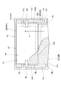
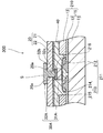
- FIG. 2 is a cross-sectional view taken along line II-II in FIG. It is a partially cutaway partial bottom view of FIG. It is a top view which shows the 1st sealing part of FIG. It is a top view which shows the 2nd sealing part of FIG. It is a top view which shows the 1st sealing part formation body for forming the 1st sealing part of FIG. It is a fragmentary sectional view which shows 2nd Embodiment of the dye-sensitized solar cell module of this invention.
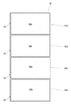
- FIG. 1 is a bottom view showing a first embodiment of the dye-sensitized solar cell module of the present invention
- FIG. 2 is a cross-sectional view taken along line II-II in FIG. 1
- FIG. 3 is a partially cutaway view of FIG. It is a notch partial bottom view.
- a dye-sensitized solar cell module (hereinafter sometimes referred to as “DSC module”) 100 includes a plurality (four in FIG. 1) of dye-sensitized solar cells (hereinafter referred to as “DSC”).
- the plurality of DSCs 50 are connected in series.
- the four DSCs 50 in the DSC module 100 may be referred to as DSCs 50A to 50D.
- each of the plurality of DSCs 50 includes a working electrode 10, a counter electrode 20 that faces the working electrode 10 and has a metal substrate 21, and a sealing portion 30 ⁇ / b> A that joins the working electrode 10 and the counter electrode 20.
- a cell space C formed by the working electrode 10, the counter electrode 20, and the annular sealing portion 30A is filled with an electrolyte 40.
- the working electrode 10 includes a transparent substrate 11 and a transparent conductive substrate 15 having a transparent conductive film 12 provided on the transparent substrate 11 and at least one oxide provided on the transparent conductive film 12 of the transparent conductive substrate 15. And a semiconductor layer 13.
- the oxide semiconductor layer 13 is disposed inside the annular sealing portion 30A.
- the transparent substrate 11 is used as a common transparent substrate for the DSCs 50A to 50D.
- An insulating material 14 is provided between the transparent substrate 11 and the sealing portion 30A. The insulating material 14 is directly fixed on the transparent substrate 11.
- the transparent conductive film 12 corresponding to the DSCs 50A to 50D may be referred to as transparent conductive films 12A to 12D.
- the first electrode is configured by the transparent conductive substrate 15.
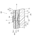
- each of the transparent conductive films 12A to 12D of each DSC 50 has a rectangular main body portion 12a indicated by a one-dot chain line (see FIG. 1). As shown in FIG. 3, the main body portion 12a has two side edge portions 12b along the arrangement direction X of the plurality of dye-sensitized solar cells 50A to 50D. For example, in two adjacent DSCs 50A and 50B, the transparent conductive film 12B in one DSC 50B has two projecting portions projecting laterally from both side edge portions 12b of the main body portion 12a with respect to the arrangement direction X of the DSCs 50A to 50D.
- the extending part 12d extends to the position outside the sealing part 30A of the DSC 50A and to the side of the side edge part 12b of the main body part 12a of the DSC 50A.
- the extending part 12d is disposed along the sealing part 30A of the DSC 50B and the sealing part 30A of the other DSC 50A.
- the two extending portions 12d are disposed so as to sandwich the main body portion 12a of the transparent conductive film 12A in the adjacent DSC 50A.
- the conductive material 60 is disposed so as to pass over the sealing portion 30A.
- a metal film is used in this embodiment.
- a metal material constituting the metal film for example, silver or copper can be used.
- the transparent conductive film 12C has a protruding portion 12c and an extending portion 12d in addition to the main body portion 12a. Also in the DSC 50D, the transparent conductive film 12D includes a projecting portion 12c and an extending portion 12d in addition to the main body portion 12a.
- the DSC 50A is already connected to the DSC 50B, and there is no other DSC 50 to be connected. For this reason, in the DSC 50A, the transparent conductive film 12A does not have the extending portion 12d.
- the counter electrode 20 includes a metal substrate 21 and a catalyst layer 22 provided on the working electrode 10 side of the metal substrate 21 to promote the catalytic reaction.
- the counter electrodes 20 are separated from each other.
- the second electrode is constituted by the counter electrode 20.
- the sealing portion 30A is provided between the transparent conductive substrate 15 and the counter electrode 20 so as to overlap the first sealing portion 31A and the annular first sealing portion 31A provided so as to overlap the insulating material 14.
- the second sealing portion 32A sandwiches the edge portion 20a of the counter electrode 20 together with the first sealing portion 31A.
- the 1st sealing part 31A which adjoined 1st sealing part 31A was integrated.
- the first sealing portion 31 is provided between an annular portion (hereinafter referred to as “annular portion”) 31 a that is not provided between two adjacent DSCs 50 and two adjacent DSCs 50.
- a part (hereinafter referred to as “partition part”) 31b that partitions the annular part 31a.
- the second sealing portions 32 ⁇ / b> A are integrated between adjacent counter electrodes 20, and the second sealing portion 32 is configured by the integrated second sealing portion 32 ⁇ / b> A.
- the thickness of the insulating material 14 is larger than the thickness of the transparent conductive film 12, and the melting point of the insulating material 14 is higher than the melting point of the first sealing portion 31A.
- reference numeral 32a represents an opening.
- the second sealing portion 32 is provided between a main body portion 32 b provided on the opposite side of the counter electrode 20 from the working electrode 10 and adjacent counter electrodes 20. And an adhesive portion 32c.
- the second sealing portion 32 is bonded to the first sealing portion 31 by the bonding portion 32c.
- the adjacent first sealing portions 31A and the adjacent second sealing portions 32A are integrated between the adjacent counter electrodes 20.
- the adjacent first sealing portions 31 ⁇ / b> A are not integrated, two adjacent sealing portions are exposed to the atmosphere between the adjacent DSCs 50.
- the adjacent first sealing portions 31A are integrated, there is one sealing portion exposed to the atmosphere between the adjacent DSCs 50. That is, since the 1st sealing part 31 is comprised by the cyclic
- the first sealing portions 31A are integrated with each other, the penetration distance of moisture and the like from the atmosphere to the electrolyte 40 is extended. For this reason, it is possible to sufficiently reduce the amount of moisture and air entering from the outside of the DSC 50 between the adjacent DSCs 50. That is, the sealing ability of the DSC module 100 can be sufficiently improved. Further, according to the DSC module 100, the adjacent first sealing portions 31A are integrated. For this reason, even if the first sealing portions 31A are integrated with each other in a state where the sealing width is smaller than that of the first sealing portion 31A that is not integrated, the partition portion 31b is formed. It becomes possible to secure the width.
- the aperture ratio can be improved, and when the DSC module 100 is used at a high temperature, the electrolyte 40 expands and an excessive stress is applied from the inside to the outside of the first sealing portion 31A. In addition, peeling of the first sealing portion 31A from the transparent conductive substrate 15 and the counter electrode 20 can be sufficiently suppressed, and excellent durability can be achieved.
- the second sealing portion 32A is bonded to the first sealing portion 31A through the gap S between the adjacent counter electrodes 20, and the edge portion 20a of the counter electrode 20 is the first sealing. It is sandwiched between the portion 31A and the second sealing portion 32A. For this reason, even if the stress in the direction away from the working electrode 10 acts on the counter electrode 20, the separation is sufficiently suppressed by the second sealing portion 32A. Further, since the second sealing portion 32A is bonded to the first sealing portion 31A through the gap S between the adjacent counter electrodes 20, it is reliably prevented that the counter electrodes 20 of the adjacent DSC 50 contact each other. Is done.
- the thickness of the insulating material 14 is larger than the thickness of the transparent conductive film 12, and the insulating material 14 has a higher melting point than the first sealing portion 31A.
- the DSC module 100 is used at a high temperature, the first sealing portion 31A is softened, and the distance between the transparent conductive substrate 15 and the counter electrode 20 may be reduced.
- the thickness of the insulating material 14 is larger than the thickness of the transparent conductive film 12, and the insulating material 14 is larger than the first sealing portion 31A. Since it has a high melting point, contact between the counter electrode 20 and the transparent conductive film 12 is sufficiently prevented.
- the transparent conductive film 12 in one DSC 50 has two projecting portions 12c and an extending portion 12d extending from each of the projecting portions 12c to the other DSC 50 side.
- the part 12d extends to the outside of the sealing part 30A of the DSC 50A and to a side position with respect to the side edge part 12b of the main body part 12a of the DSC 50A. Then, the extending portion 12 d and the metal substrate 21 of the counter electrode 20 in the other DSC 50 are connected via the conductive material 60.
- the transparent conductive film 12 of one DSC 50 and the counter electrode 20 of the other DSC 50 are outside the light receiving area including the sealing portions 30A of all the DSCs 50A to 50D. It is connected. In other words, a connection point that does not contribute to power generation in the DSC module 100 is provided outside the light receiving area. Therefore, the aperture ratio can be improved.
- the transparent conductive film 12 of one DSC 50 and the counter electrode 20 of the other DSC 50 are connected outside the light receiving area, the connection portion between the transparent conductive film 12 and the conductive material 60, and the counter electrode 20 and the conductive material. It is also possible to increase the area of the connection point with 60.
- the extending portion 12d of the transparent conductive film 12 in one DSC 50 is positioned laterally from the overhanging portion 12c to the outside of the sealing portion 30A of the other DSC 50A and to the side edge portion 12b of the main body portion 12a of the DSC 50A. It extends to. That is, the transparent conductive film 12A of the DSC 50B is provided in the immediate vicinity of the counter electrode 20 of the adjacent DSC 50A. For this reason, the conductive material 60 can be shortened, and the operator's hand is not easily caught by the conductive material 60.
- connection reliability in the DSC module 100 is sufficient. Can be improved.
- the conductive material 60 is sufficiently prevented from coming into contact with the counter electrode 20 of the adjacent DSC 50, the adjacent counter electrodes 20 are sufficiently prevented from being electrically connected by the conductive material 60. As a result, it is possible to sufficiently prevent malfunction of the DSC module 100.
- the counter electrode 20 of one DSC 50 and the extending portion 12d of the transparent conductive film 12 of the other DSC 50 are connected by a conductive material 60 made of a metal film. . For this reason, it is possible to reduce the unevenness on the surface of the counter electrode 20 opposite to the working electrode 1, and it is possible to stably install the DSC module 100 on a flat surface such as the inner wall surface of the case.
- a transparent conductive substrate 15 formed by forming a transparent conductive film 12 on one transparent substrate 11 is prepared.
- the material which comprises the transparent substrate 11 should just be a transparent material, for example, as such a transparent material, glass, such as borosilicate glass, soda lime glass, white plate glass, quartz glass, polyethylene terephthalate (PET), for example , Polyethylene naphthalate (PEN), polycarbonate (PC), and polyethersulfone (PES).
- PET polyethylene terephthalate
- PEN Polyethylene naphthalate
- PC polycarbonate
- PES polyethersulfone
- the thickness of the transparent substrate 11 is appropriately determined according to the size of the DSC module 100 and is not particularly limited, but may be in the range of 50 to 10,000 ⁇ m, for example.
- Examples of the material for forming the transparent conductive film 12 include tin-doped indium oxide (Indium-Tin-Oxide: ITO), tin oxide (SnO 2 ), and fluorine-doped tin oxide (Fluorine-doped-Tin-Oxide: FTO).
- Examples include conductive metal oxides.
- the transparent conductive film 12 may be a single layer or a laminate of a plurality of layers made of different conductive metal oxides. When the transparent conductive film 12 is composed of a single layer, the transparent conductive film 12 is preferably composed of FTO because it has high heat resistance and chemical resistance.
- the transparent conductive film 12 it is preferable to use a laminate composed of a plurality of layers as the transparent conductive film 12 because the characteristics of each layer can be reflected. Among these, it is preferable to use a laminate of a layer made of ITO and a layer made of FTO. In this case, the transparent conductive film 12 having high conductivity, heat resistance and chemical resistance can be realized.
- the thickness of the transparent conductive film 12 may be in the range of 0.01 to 2 ⁇ m, for example.
- a sputtering method As a method for forming the transparent conductive film 12, a sputtering method, a vapor deposition method, a spray pyrolysis method (SPD), a CVD method, or the like is used.
- patterning is performed on the transparent conductive film 12 with, for example, a YAG laser or a CO 2 laser as follows. That is, patterning is performed so that the four transparent conductive films 12A to 12D corresponding to the DSCs 50A to 50D have the rectangular main body portion 12a and the overhanging portion 12c. At this time, for the transparent conductive films 12B to 12D corresponding to the DSCs 50B to 50D, not only the rectangular main body 12a and the overhanging part 12c but also an extending part 12d extending from the overhanging part 12c to the adjacent DSC 50 side. Patterning is performed to form.
- the oxide semiconductor layer 13 is formed on the main body 12 a of the transparent conductive film 12.
- the oxide semiconductor layer 13 is formed by printing a porous oxide semiconductor layer forming paste containing oxide semiconductor particles, followed by firing.
- the oxide semiconductor layer forming paste contains a resin such as polyethylene glycol and a solvent such as terpineol in addition to the oxide semiconductor particles.
- the oxide semiconductor particles include titanium oxide (TiO 2 ), silicon oxide (SiO 2 ), zinc oxide (ZnO), tungsten oxide (WO 3 ), niobium oxide (Nb 2 O 5 ), and strontium titanate (SrTiO 3 ).
- the thickness of the oxide semiconductor layer 13 may be 0.5 to 50 ⁇ m, for example.
- a method for printing the oxide semiconductor layer forming paste for example, a screen printing method, a doctor blade method, a bar coating method, or the like can be used.
- the firing temperature varies depending on the material of the oxide semiconductor particles, but is usually 350 to 600 ° C.
- the firing time also varies depending on the material of the oxide semiconductor particles, but is usually 1 to 5 hours.
- the insulating material 14 disposed between the adjacent DSCs 50 is directly fixed on the transparent substrate 11.
- the insulating material 14 is provided to prevent the transparent conductive film 12 on the transparent substrate 11 and the counter electrode 20 from coming into contact with each other and short-circuiting. Therefore, the insulating material 14 only needs to have a higher melting point than the first sealing portion 31A.
- an inorganic material such as low-melting glass, polyimide, an ultraviolet curable resin, a thermoplastic resin, or the like is used.
- an inorganic substance is preferable because it effectively prevents leakage of the electrolyte 40.
- the thickness of the insulating material 14 is usually 1 to 200 ⁇ m, preferably 3 to 10 ⁇ m.
- a photosensitizing dye is supported on the oxide semiconductor layer 13 of the working electrode 10.
- the working electrode 10 is immersed in a solution containing a photosensitizing dye, the photosensitizing dye is adsorbed on the oxide semiconductor layer 13, and then the excess photosensitizer is added with the solvent component of the solution.
- the photosensitizing dye may be adsorbed to the oxide semiconductor layer 13 by washing away the dye and drying it.
- the photosensitizing dye can be absorbed into the oxide semiconductor layer 13. 13 can be carried.
- the photosensitizing dye examples include a ruthenium complex having a ligand containing a bipyridine structure, a terpyridine structure, and the like, and organic dyes such as porphyrin, eosin, rhodamine, and merocyanine.
- the electrolyte 40 is disposed on the oxide semiconductor layer 13.
- the electrolyte 40 includes, for example, a redox couple such as I ⁇ / I 3 ⁇ and an organic solvent.
- a redox couple such as I ⁇ / I 3 ⁇
- organic solvent acetonitrile, methoxyacetonitrile, methoxypropionitrile, propionitrile, ethylene carbonate, propylene carbonate, diethyl carbonate, ⁇ -butyrolactone, and the like can be used.
- the redox pair include I ⁇ / I 3 ⁇ and bromine / bromide ion pairs.
- a gelling agent may be added to the volatile solvent.
- the electrolyte 40 may be composed of an ionic liquid electrolyte made of a mixture of an ionic liquid and a volatile component.
- the ionic liquid for example, a known iodine salt such as a pyridinium salt, an imidazolium salt, or a triazolium salt, and a room temperature molten salt that is in a molten state near room temperature is used.
- a room temperature molten salt for example, 1-ethyl-3-methylimidazolium bis (trifluoromethylsulfonyl) imide is preferably used.
- the volatile component include the above organic solvents, LiI, I 2 , 4-t-butylpyridine, N-methylbenzimidazole, and the like.
- the 1st sealing part formation body 131 for forming the 1st sealing part 31 is prepared.
- the 1st sealing part formation body 131 can be obtained by preparing the sealing resin film of 1 sheet, and forming the square-shaped opening 131a according to the number of DSC50 in the sealing resin film.
- the first sealing portion forming body 131 has a structure in which a plurality of first sealing portion forming bodies 131A are integrated.
- sealing resin film examples include resins such as ionomer, ethylene-vinyl acetic anhydride copolymer, ethylene-methacrylic acid copolymer, ethylene-vinyl alcohol copolymer, ultraviolet curable resin, and vinyl alcohol polymer. Is mentioned.
- the first sealing portion forming body 131 is adhered on the working electrode 10. At this time, the first sealing portion forming body 131 is bonded to the working electrode 10 so as to overlap the insulating material 14.
- the first sealing portion forming body 131 can be adhered to the working electrode 10 by heating and melting the first sealing portion forming body 131.
- the first sealing portion forming body 131 is bonded to the working electrode 1 so that the main body portion 12 a of the transparent conductive film 2 is disposed inside the first sealing portion forming body 131.
- the counter electrode 20 includes the metal substrate 21 and the conductive catalyst layer 22 that is provided on the working electrode 10 side of the metal substrate 21 and promotes the reduction reaction on the surface of the counter electrode 20.
- the metal substrate 21 is formed by, for example, forming a film made of a corrosion-resistant metal material such as titanium, nickel, platinum, molybdenum, tungsten, aluminum, and stainless steel or a conductive oxide such as ITO or FTO on the transparent substrate 11 described above. Composed.
- the thickness of the metal substrate 21 is appropriately determined according to the size of the DSC module 100 and is not particularly limited, but may be, for example, 0.005 to 0.1 mm.
- the catalyst layer 22 is composed of platinum, a carbon-based material, a conductive polymer, or the like.
- carbon nanotubes are suitably used as the carbon-based material.
- the first sealing portion forming body 131 bonded to the counter electrode 20 and the first sealing portion forming body 131 bonded to the working electrode 10 are superposed and heated while pressurizing the first sealing portion forming body 131. Melt.
- the first sealing portion 31 is formed between the working electrode 10 and the counter electrode 20.
- the formation of the first sealing portion 31 may be performed under atmospheric pressure or under reduced pressure, but is preferably performed under reduced pressure.
- a second sealing portion 32 is prepared.
- the second sealing portion 32 has a structure in which a plurality of first sealing portions 32A are integrated.
- the second sealing portion 32 can be obtained by preparing a single sealing resin film and forming a rectangular opening 32a corresponding to the number of DSCs 50 in the sealing resin film.
- the second sealing portion 32 is bonded to the counter electrode 20 so as to sandwich the edge portion 20 a of the counter electrode 20 together with the first sealing portion 31.
- the adhesion of the second sealing portion 32 to the counter electrode 20 can be performed by heating and melting the second sealing portion 32.
- the sealing resin film examples include resins such as ionomer, ethylene-vinyl acetic anhydride copolymer, ethylene-methacrylic acid copolymer, ethylene-vinyl alcohol copolymer, ultraviolet curable resin, and vinyl alcohol polymer. Is mentioned.
- the constituent material of the sealing resin film for forming the second sealing portion 32 preferably has a higher melting point than the constituent material of the sealing resin film for forming the first sealing portion 31. In this case, since the second sealing portion 32A is harder than the first sealing portion 31A, it is possible to effectively prevent contact between the counter electrodes 20 of the adjacent DSCs 50. Further, since the first sealing portion 31A is softer than the second sealing portion 32A, the stress applied to the sealing portion 30A can be effectively relieved.
- a paste containing a metal material constituting the conductive material 60 is prepared, and this paste is applied from the counter electrode 20 to the extending portion 12d of the transparent conductive film 12 of the adjacent DSC 50 and cured.
- a low-temperature curable paste that can be cured at a temperature of 90 ° C. or lower.
- the DSC module 100 is obtained as described above.
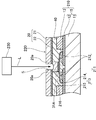
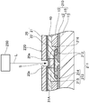
- FIG. 7 is a partial cross-sectional view showing a second embodiment of the DSC module of the present invention.
- the same or equivalent components as those in the first embodiment are denoted by the same reference numerals, and redundant description is omitted.
- the working electrode 210 is disposed between the first sealing portion 31 ⁇ / b> A and the transparent substrate 11 in place of the insulating material 14, and the transparent conductive film of the adjacent DSC 50.
- 12 is different from the DSC module 100 of the first embodiment in that it includes a wiring portion 211 provided so as to connect 12 and a low thermal conductive layer 216 provided between the wiring portion 211 and the first sealing portion 31A.
- the wiring section 211 includes a current collecting wiring 212 provided on each of the transparent conductive films 12 of adjacent DSCs 50 and a wiring protection layer 213 that protects the current collecting wiring 212 from the electrolyte 40.
- the wiring protective layer 213 covers the current collecting wiring 212 to protect it from the electrolyte 40, and covers the first wiring protective layer 214 in direct contact with the transparent substrate 11, and the first wiring protective layer 214 to cover the current collecting wiring 212 with the electrolyte 40.
- a second wiring protective layer 215 for protecting from the above.
- the low thermal conductive layer 216 is made of a low thermal conductive material having lower thermal conductivity than the material constituting each of the first sealing portion 31A and the wiring protective layer 213.
- a low thermal conductivity material for example, when polyethylene is used as the first sealing portion 31A, glass is used as the first wiring protection layer 214, and polyimide is used as the second wiring protection layer 215, polypropylene, Resins such as polystyrene can be used.
- the thickness of the low thermal conductive layer 216 is, for example, 20 to 60 ⁇ m.
- the low thermal conductive layer 216 having lower thermal conductivity than the first sealing portion 31A and the wiring protective layer 213 is provided between the first sealing portion 31A and the wiring protective layer 213. Is provided. For this reason, even if a certain DSC 50 is locally heated due to the heat of sunlight, etc., and the low thermal conductive layer 216 is locally heated, the low thermal conductive layer 216 is formed of the first sealing portion 31A and the wiring protective layer. Since it has thermal conductivity lower than 213, its fluidity is unlikely to decrease. For this reason, the relative positional relationship between the counter electrodes 20 of adjacent DSCs can be sufficiently maintained. That is, since the fluidity of the low thermal conductive layer 216 is not easily lowered, the edge 20a of the counter electrode 20 is more sufficiently suppressed from approaching the transparent conductive film 12. For this reason, it is more fully suppressed that counter electrodes 20 contact.
- the difference between the thermal conductivity of the low thermal conductive layer 216 and the thermal conductivity of the layer having the lowest thermal conductivity among the first sealing portion 31A and the wiring protective layer 213 is preferably 0.1 W / m ⁇ K or more, more preferably 0.10 to 0.6 W / m ⁇ K, still more preferably 0.15 to 0.4 W / m ⁇ K.
- the relative positional relationship between the counter electrodes 20 of adjacent DSCs 50 can be more sufficiently maintained.
- the manufacturing method of the DSC module 200 is the first embodiment in that instead of forming the insulating material 14 between the first sealing portion 31A and the transparent substrate 11, the wiring portion 211 and the low thermal conductive layer 216 are formed sequentially. This is different from the manufacturing method of the DSC module 100 of FIG.
- the wiring part 211 is performed before the step of bonding the first sealing part forming body 131 to the working electrode 10. Specifically, in the wiring portion 211, the current collecting wiring 212 is formed on each of the two adjacent transparent conductive films 12, and then the wiring protective layer 213 is formed so as to cover the current collecting wiring 212. At this time, the current collector wiring 212 can be formed by applying a paste containing silver or the like to the surface of the transparent conductive film 12, drying, and firing. For the first wiring protective layer 214, a paste containing the material constituting the first wiring protective layer 214 is applied to the surfaces of the current collector wiring 211, the transparent conductive film 12, and the transparent substrate 11, and after drying, as necessary. It can be formed by firing. The second wiring protective layer 215 can be obtained by applying a paste containing a material constituting the second wiring protective layer 215 to the surface of the first wiring protective layer 214, drying it, and baking it as necessary. .
- the low thermal conductive layer 216 can be formed by applying a paste containing the low thermal conductive material to the surface of the wiring protective layer 213 and drying it.
- the counter electrode 20 may be prepared by preparing a plurality of counter electrodes 20 in advance, as in the first embodiment, but the counter electrode 20 may be manufactured as follows. This is preferable from the viewpoint of improving production efficiency.
- one counter electrode forming body 220 is prepared. Then, the single counter electrode forming body 220 is bonded so as to close the entire opening 131 a of the first sealing portion forming body 131.
- the first sealing portion forming body 131 bonded to the counter electrode forming body 220 and the first sealing portion forming body 131 bonded to the working electrode 10 are overlapped, and the first sealing portion forming body 131 is pressurized. Heat and melt while.
- the first sealing portion 31 ⁇ / b> A is formed between the working electrode 10 and the counter electrode forming body 220.
- the counter electrode forming body 220 is cut by laser processing to be divided into a plurality of counter electrodes 20. Specifically, as shown in FIG. 9, the counter electrode forming body 220 is irradiated with the laser light L from the laser light source 230 on a portion of the counter electrode forming body 220 that is in contact with the first sealing portion 31 ⁇ / b> A. Is divided into a plurality of counter electrodes 20.
- the cutting of the counter electrode forming body 220 is performed by heating and melting the cut portion.
- the low thermal conductive layer 216 having lower thermal conductivity than the first sealing portion 31A is provided between the first sealing portion 31A and the wiring protective layer 213 of the wiring portion 211, the counter electrode is formed. While cutting the body 220, the diffusion of heat at the cut portion is sufficiently suppressed. For this reason, the counter electrode forming body 220 can be efficiently cut.
- a pulse laser light source is used as the laser light source 230.
- the wavelength of the laser beam L may be 1000 nm or more, preferably 1000 to 2000 nm, and more preferably 1000 to 1200 nm.
- the pulse width of the laser beam L is not particularly limited, but is usually 150 ns or less, preferably 100 ns or less. However, it is preferably 5 ns or more. In this case, a sufficient amount of heat can be applied to the cut portion of the counter electrode forming body 220.
- the irradiation energy per unit scanning distance is preferably 0.01 to 0.3 J / mm, and more preferably 0.06 to 0.09 J / mm.
- the number of times of cutting per place may be one time or a plurality of times, but one time is preferable from the viewpoint of production efficiency.
- FIG. 10 is a partial cross-sectional view showing a third embodiment of the DSC module of the present invention.
- the same or equivalent components as those in the first and second embodiments are denoted by the same reference numerals, and redundant description is omitted.
- the low thermal conductive layer 216 is replaced with the first sealing portion 31 ⁇ / b> A and the counter electrode 20 instead of between the first sealing portion 31 ⁇ / b> A and the transparent substrate 11. It is different from the DSC module 200 of the second embodiment in that it is provided in between.
- the low thermal conductive layer 216 having lower thermal conductivity than the first sealing portion 31A and the wiring protective layer 213 is provided between the first sealing portion 31A and the counter electrode 20. ing. For this reason, even if a certain DSC 50 is locally heated due to the heat of sunlight, etc., and the low thermal conductive layer 216 is locally heated, the low thermal conductive layer 216 is formed of the first sealing portion 31A and the wiring protective layer. Since it has thermal conductivity lower than 213, its fluidity is unlikely to decrease. For this reason, the relative positional relationship between the counter electrodes 20 of the adjacent DSCs 50 can be sufficiently maintained. That is, since the fluidity of the low thermal conductive layer 216 is not easily lowered, the edge 20a of the counter electrode 20 is more sufficiently suppressed from approaching the transparent conductive film 12. For this reason, it is more fully suppressed that counter electrodes 20 contact.
- the difference between the thermal conductivity of the low thermal conductivity layer 216 and the thermal conductivity of the layer having the lowest thermal conductivity among the first sealing portion 31A and the wiring protective layer 213 is the same as in the second embodiment. Therefore, it is preferably 0.1 W / m ⁇ K or more, more preferably 0.1 to 0.6 W / m ⁇ K, and still more preferably 0.15 to 0.4 W / m ⁇ K.
- the low thermal conductive layer 216 is not fixed to the working electrode 10 before the first sealing portion forming body 131 is bonded to the working electrode 10, but is first sealed to the counter electrode 20. This is different from the manufacturing method of the DSC module 200 of the second embodiment in that it is fixed to the counter electrode 20 before the step of bonding the part forming body 131.
- the manufacturing method of the DSC module 300 as in the manufacturing method of the DSC module 200 of the second embodiment, it is possible to produce the counter electrode 20 by irradiating the laser light L from the laser light source 230. It is preferable from the viewpoint of improvement.
- the cutting of the counter electrode forming body 220 for forming the counter electrode 20 is performed by causing the cut portion to generate heat and melting.
- the low thermal conductive layer 216 having lower thermal conductivity than the first sealing portion 31A is provided between the first sealing portion 31 and the counter electrode forming body 220, the counter electrode forming body 220 is cut.
- the diffusion of heat at the cut portion is sufficiently suppressed.
- the low thermal conductive layer 216 is in direct contact with the counter electrode forming body 220. For this reason, while the counter electrode forming body 220 is being cut, it is possible to effectively suppress the heat generated at the cutting portion from diffusing, and the counter electrode forming body 220 can be cut more efficiently.
- FIG. 12 is a partial cross-sectional view showing a fourth embodiment of the dye-sensitized solar cell module of the present invention.
- the same or equivalent components as those in the first to third embodiments are denoted by the same reference numerals, and redundant description is omitted.
- the DSC module 400 of this embodiment does not have the low thermal conductive layer 216 between the first sealing portion 31 ⁇ / b> A and the wiring protection layer 213,
- the partition portion 31b is different from the DSC module 200 of the second embodiment in that the partition portion 31b is made of a low thermal conductivity material having a lower thermal conductivity than the annular portion 31a.
- the DSC module 400 of the present embodiment even if a certain DSC 50 is locally heated due to the heat of sunlight or the like, and the partition portion 31b of the first sealing portion 31 is locally heated, The partition portion 31b that has reached a high temperature has a lower thermal conductivity than the annular portion 31a that is not provided between the two adjacent DSCs 50, so that heat is not easily transmitted to the adjacent DSC 50, and the adjacent DSC 50 is deteriorated. Can be sufficiently suppressed.
- the material constituting the annular portion 31a of the first sealing portion 31 is ionomer, ethylene-vinyl acetic anhydride copolymer, ethylene-methacrylic acid copolymer, ethylene-vinyl alcohol copolymer, ultraviolet curable resin, And it selects from resin, such as a vinyl alcohol polymer, suitably.
- the material constituting the partition portion 31b of the first sealing portion 31 may be a low thermal conductivity material having lower thermal conductivity than the material constituting the annular portion 31a, and examples thereof include resins such as polypropylene and polystyrene. It is done.
- the annular portion 31a is formed on the working electrode 210, and then the partition portion 31b is formed by vacuum lamination on the inside of the annular portion 31a and on the wiring portion 211. What is necessary is just to form.
- the difference between the thermal conductivity of the annular portion 31a of the first sealing portion 31A and the thermal conductivity of the partition portion 31b is 0.1 W / m ⁇ K or more, more preferably 0.10 to It is 0.6 W / m ⁇ K, more preferably 0.15 to 0.4 W / m ⁇ K.
- each of the transparent conductive films 12B to 12D has two projecting portions 12c, but the transparent conductive films 12B to 12D do not need to have two projecting portions 12c. You may have only one. In this case, the transparent conductive films 12B to 12D have only one extending portion 12d.
- the transparent conductive films 12B, 12C, and 12D have the two overhanging portions 12c and the two extending portions 12d. From the viewpoint of achieving the first object of being able to be improved and having excellent durability, in the transparent conductive films 12B, 12C, and 12D, the overhanging portion 12c and the extending portion 12d are not necessarily required. It can be omitted.
- the second sealing portion 32A is bonded to the first sealing portion 31A, but the second sealing portion 32A is not bonded to the first sealing portion 31A. May be.
- the first sealing portion 31A and the second sealing portion 32A are made of the same material, in the sealing portion 30A, the first sealing portion 31A is adjacent to the counter electrode.
- the counter electrode 20 extends to the opposite side of the working electrode 10 through the gap S between the two electrodes 20, and is bonded to the edge 20a of the counter electrode 20.
- the first sealing portion 31A extends to the surface of the counter electrode 20 opposite to the working electrode 10 and is bonded to the edge 20a of the counter electrode 20. For this reason, even if a stress in a direction away from the working electrode 10 acts on the counter electrode 20, the separation is sufficiently suppressed by the first sealing portion 31A.
- the first sealing portion 31A extends to the surface of the counter electrode 20 opposite to the working electrode 10 and is bonded to the edge portion 20a of the counter electrode 20, the intrusion distance of moisture or the like from the atmosphere to the electrolyte 40 is increased. It extends more. For this reason, between the adjacent DSCs 50, the amount of moisture and air entering from the outside of the DSC 50 can be more sufficiently reduced.
- the sealing part 30A is composed of the first sealing part 31A and the second sealing part 32A, but the second sealing part 32A may be omitted.
- the thickness of the insulating material 14 is larger than the thickness of the transparent conductive film 12, and the melting point of the insulating material 14 is higher than the melting point of the first sealing portion 31.
- the thickness of 14 may be equal to or less than the thickness of the transparent conductive film 12, and the melting point of the insulating material 14 may be equal to or less than the melting point of the first sealing portion 31.
- the insulating material 14 is provided. However, when a material having a sufficiently high melting point is used as the first sealing portion 31A, the counter electrode 20 and the transparent conductive film 12 are sufficiently short-circuited. Can be omitted, and can be omitted.
- the annular first sealing portions 31A of the adjacent DSCs 50 are integrated with each other, but the connection reliability can be sufficiently improved while improving the aperture ratio.
- the annular first sealing portions 31A of the adjacent DSCs 50 do not necessarily have to be integrated. That is, the annular first sealing portions 31A may be separated from each other.
- the conductive material 60 is made of a metal film.
- the conductive material 60 is not limited to a metal film, and may be made of a jumper wire or the like.
- the partition part 31b of the 1st sealing parts 31 is comprised with the low heat conductive material which has lower thermal conductivity than the cyclic
- the 1st sealing part 31 is comprised.
- the partition portion 31b is made of the same material as the annular portion 31a, and the portion of the first wiring protective layer 214 or the second wiring protective layer 215 provided between the partition portion 31b and the transparent substrate 11 is an annular portion. You may be comprised with the heat conductive material which has heat conductivity lower than the part provided between 31a and the transparent substrate 11. FIG.
- the partition portion 31b of the first sealing portion 31 is made of a low thermal conductivity material having a lower thermal conductivity than the annular portion 31a, and the first wiring protection layer 214 or the second wiring protection layer 215 Among these, the part provided between the partition part 31 b and the transparent substrate 11 may be made of a heat conductive material having lower thermal conductivity than the part provided between the annular part 31 a and the transparent substrate 11. .
- the wiring part 211 is provided, but the wiring part 211 is not necessarily required and can be omitted.
- a transparent conductive substrate was prepared by forming a transparent conductive film made of FTO having a thickness of 1 ⁇ m on a transparent substrate made of glass having a thickness of 1 mm. Then, patterning was performed so as to form four transparent conductive films arranged in a row by a CO 2 laser (V-460 manufactured by Universal System). The patterning was performed so that each of the four transparent conductive films had a rectangular main body of 3 cm ⁇ 5 cm, and the interval between the main bodies was 0.5 mm. Of the four transparent conductive films, three transparent conductive films are transparent conductive films corresponding to the adjacent DSCs from the two projecting parts projecting from both side edges of the main body part and the two projecting parts.
- An extension portion extending to a side position with respect to the side edge portion of the main body portion of the film is formed.
- the length of the overhang portion in the overhang direction was 1 cm, and the width of the overhang portion was 3 mm. Further, the width of the extending part was 2 mm, and the length of the extending part in the extending direction was 2 cm.
- an oxide semiconductor layer forming paste containing titania was applied onto the main body of the transparent conductive film, dried, and then fired at 500 ° C. for 1 hour. Thus, a working electrode having the oxide semiconductor layer 13 was obtained.
- the paste containing the low melting point glass is applied to the region between the main body portions by screen printing and then baked, and the insulating material (melting point: 495 ° C.) made of the low melting point glass in the region between the adjacent main body portions. Formed. At this time, the thickness of the insulating material was 60 ⁇ m.
- the working electrode is immersed overnight in a dye solution containing 0.3 mmol of a photosensitizing dye composed of N719 and a solvent in which acetonitrile and tert-butanol are mixed at a volume ratio of 1: 1. Then, it was taken out and dried, and a photosensitizing dye was supported on the oxide semiconductor layer.
- a photosensitizing dye composed of N719 and a solvent in which acetonitrile and tert-butanol are mixed at a volume ratio of 1: 1.
- an electrolyte made of iodine redox was applied on the oxide semiconductor layer and dried to place the electrolyte.
- the first sealing part forming body is prepared as a single sealing resin film made of a 12 cm ⁇ 5 cm ⁇ 50 ⁇ m ethylene-methacrylic acid copolymer (trade name: Nucrel, Mitsui-Dupont Polychemical Co., Ltd.) It was obtained by forming four rectangular openings in the sealing resin film. At this time, the 1st sealing part formation body was produced so that each opening might become a magnitude
- the first sealing portion forming body was adhered to the working electrode by heating and melting.
- Each counter electrode was prepared by forming a catalyst layer made of platinum having a thickness of 10 nm on a 2.95 cm ⁇ 5 cm ⁇ 40 ⁇ m titanium foil by sputtering.
- another first sealing portion forming body was prepared, and this first sealing portion forming body was adhered to the surface of the counter electrode facing the working electrode in the same manner as described above.
- the first sealing portion forming body bonded to the working electrode and the first sealing portion forming body bonded to the counter electrode were opposed to each other, and the first sealing portion forming bodies were overlapped with each other. And in this state, the 1st sealing part formation body was heat-melted, pressing the 1st sealing part formation body. Thus, the first sealing portion was formed between the working electrode and the counter electrode.
- the second sealing portion prepares one sealing resin film made of maleic anhydride-modified polyethylene (trade name: Binnel, manufactured by DuPont) having a size of 13 cm ⁇ 6 cm ⁇ 50 ⁇ m. It was obtained by forming four rectangular openings. At this time, each opening has a size of 2.8 cm ⁇ 4.8 cm ⁇ 50 ⁇ m, the width of the outer peripheral portion is 1.5 mm, and the width of the partition portion that partitions the inner opening of the outer peripheral portion is 1 mm.
- a second sealing portion was prepared. The second sealing part was bonded to the counter electrode so as to sandwich the edge of the counter electrode together with the first sealing part. At this time, the first sealing portion and the second sealing portion were bonded to the counter electrode and the first sealing portion by heating and melting while pressing the second sealing portion against the counter electrode.
- a low temperature curing type silver paste (Fujikura Kasei Co., Ltd., D-500) is prepared and applied from the counter electrode to the extended portion of the transparent conductive film corresponding to the adjacent DSC and cured at 30 ° C. for 12 hours. It was.
- a metal film made of silver and connecting the counter electrode and the extending portion of the transparent conductive film corresponding to the adjacent DSC was formed.
- the size of the metal film was 7 mm ⁇ 10 mm ⁇ 10 ⁇ m.
- a DSC module was thus obtained. In the obtained DSC module, the distance D in the DSC arrangement direction between adjacent counter electrodes was 0.5 mm, and the width W of the sealing portion (partition portion) was 1 mm.
- Example 2 As shown in Table 1, the transparent conductive film, the first sealing part, the second sealing part, the insulating material, the spacing D in the DSC arrangement direction between adjacent counter electrodes, and the width W of the sealing part (partition part) are changed.
- a DSC module was produced in the same manner as in Example 1 except that.
- Examples 4 to 7 As shown in Table 1, the transparent conductive film, the first sealing part, the second sealing part, the insulating material, the spacing D in the DSC arrangement direction between adjacent counter electrodes, and the width W of the sealing part (partition part) are changed.
- a DSC module was produced in the same manner as in Example 1 except that.
- a transparent conductive substrate was prepared by forming a transparent conductive film made of FTO having a thickness of 1 ⁇ m on a transparent substrate made of glass having a thickness of 1 mm. Then, patterning was performed so as to form four transparent conductive films arranged in a row by a CO 2 laser (V-460 manufactured by Universal System). The patterning was performed so that the four transparent conductive films had a rectangular main body portion of 3 cm ⁇ 5 cm, and the interval between the main body portions was 0.5 mm. Of the four transparent conductive films, three transparent conductive films are transparent conductive films corresponding to the adjacent DSCs from the two projecting parts projecting from both side edges of the main body part and the two projecting parts.
- An extension portion extending to a side position with respect to the side edge portion of the main body portion of the film is formed.
- the length of the overhang portion in the overhang direction was 1 cm, and the width of the overhang portion was 3 mm. Further, the width of the extending part was 2 mm, and the length of the extending part in the extending direction was 2 cm.
- an oxide semiconductor layer forming paste containing titania was applied onto the main body of the transparent conductive film, dried, and then fired at 500 ° C. for 1 hour.
- a paste containing silver was applied on the transparent conductive film, dried, and then fired at 500 ° C. for 1 hour to obtain a current collector wiring.
- a paste containing a low-melting glass is applied by screen printing so as to include the current collecting wiring formed on each of the adjacent transparent conductive films, and then baked at 500 ° C. for 1 hour to form a first wiring protective layer. Formed.
- the low-melting glass had a thermal conductivity of 0.76 W / m ⁇ K.
- a paste containing polyimide was applied to the first wiring protective layer by screen printing and then heated at 350 ° C. for 1 hour to form a second wiring protective layer.
- the thermal conductivity of the polyimide was 0.31 W / m ⁇ K.
- a paste containing polypropylene hereinafter referred to as “PP” was applied on the second wiring protective layer and then dried to obtain a low thermal conductive layer having a thickness of 0.06 mm.
- the thermal conductivity of PP was 0.125 W / m ⁇ K.
- Example 2 a first sealing portion forming body for forming the first sealing portion was prepared.
- the thermal conductivity of the nucleure which comprises a 1st sealing part formation body was 0.33 W / m * K.
- the first sealing portion forming body was bonded to the working electrode by heating and melting.
- the counter electrode forming body was prepared by forming a catalyst layer made of platinum having a thickness of 10 nm on a 2.95 cm ⁇ 5 cm ⁇ 40 ⁇ m titanium foil by sputtering. Further, another first sealing portion forming body was prepared, and this first sealing portion forming body was adhered to the surface of the counter electrode forming body facing the working electrode in the same manner as in Example 1. .
- the first sealing portion forming body bonded to the working electrode and the first sealing portion forming body bonded to the counter electrode forming body were opposed to each other, and the first sealing portion forming bodies were overlapped with each other. And in this state, the 1st sealing part formation body was heat-melted, pressing the 1st sealing part formation body. Thus, the first sealing portion was formed between the working electrode and the counter electrode forming body.
- one counter electrode forming body was cut by laser processing and divided into four counter electrodes.
- the laser processing conditions at this time were as follows. (1) Laser light source Yb: fiber laser (oscillation wavelength: 1090 nm, product name: MD-F3000, manufactured by Keyence Corporation) (2) Laser pulse width 50 ns (3) Irradiation energy per unit scanning distance 0.06 J / mm
- the second sealing portion prepares one sealing resin film made of maleic anhydride-modified polyethylene (trade name: Binnel, manufactured by DuPont) having a size of 13 cm ⁇ 6 cm ⁇ 50 ⁇ m. It was obtained by forming four rectangular openings. At this time, each opening is 2.8 cm ⁇ 4.8 cm ⁇ 50 ⁇ m in size, the width of the outer peripheral portion is 1.5 mm, and the width of the partition that partitions the inner opening of the outer peripheral portion is 1 mm.
- Two sealing parts were produced. The second sealing part was bonded to the counter electrode so as to sandwich the edge of the counter electrode together with the first sealing part. At this time, the first sealing portion and the second sealing portion were bonded to the counter electrode and the first sealing portion by heating and melting while pressing the second sealing portion against the counter electrode.
- a low temperature curing type silver paste (Fujikura Kasei Co., Ltd., D-500) is prepared and applied from the counter electrode to the extended portion of the transparent conductive film corresponding to the adjacent DSC and cured at 30 ° C. for 12 hours. It was. Thus, a conductive material made of silver and connecting the counter electrode and the extending portion of the transparent conductive film corresponding to the adjacent DSC was formed. The size of the conductive material was 7 mm ⁇ 10 mm ⁇ 10 ⁇ m. A DSC module was thus obtained.
- Example 9 An annular portion that is not formed between two adjacent DSCs without forming a low thermal conductive layer, and a partition portion that is provided between two adjacent DSCs and partitions the annular portion is sequentially formed by vacuum lamination, A DSC module was produced in the same manner as in Example 8 except that the first sealing portion forming body was prepared so that the portion was composed of nucleolate and the partition portion was composed of polypropylene.
- the upper part in the column of the material, melting point and thermal conductivity of the first sealing part shows the material, melting point and thermal conductivity of the annular part, and the lower part shows the material, melting point of the partition part. And the thermal conductivity is shown.
- Example 5 A transparent conductive film that does not have an extending part is formed, and the second sealing part is not used, and the first sealing part has a width of 1 mm and an opening of 2.8 mm ⁇ 4.8 mm 4 Two square annular sealing portions, the interval between the sealing portions of adjacent DSCs was 2 mm, and the edge of the counter electrode and the transparent conductive film of the adjacent DSC were connected via a jumper wire between the sealing portions.
- a DSC module was produced in the same manner as in Example 1 except for the above.
- a DSC module was produced in the same manner as in Example 1 except that the first sealing portion was four square annular sealing portions having a width of 1 mm and an opening of 2.8 mm ⁇ 4.8 mm.
- the aperture ratio was measured in order to examine whether or not the first object was achieved.
- the results are shown in Table 1.
- the acceptance criteria for the aperture ratio were as follows. Pass: 90% or more
- the power generation efficiency immediately after manufacture was measured, and then the power generation efficiency was measured in an environment of 85 ° C. was measured for a 30% drop.
- the power generation efficiency is energy conversion efficiency with respect to incident light of AM 1.5 and 100 mW / cm 2 , and is a value when only the area of the titanium oxide porous film is considered as the light incident area. This time was called durability time, and was used as an index of durability of the DSC module.
- the results are shown in Table 1.
- the acceptance criteria for durability were as follows. Pass: More than 1000 hours
- the DSC module of the present invention can improve the aperture ratio and has excellent durability.
- the counter electrode of one DSC and the extending portion of the transparent conductive film of the other DSC are connected by a metal film. For this reason, it is considered that there is no worry that the operator's hand will be caught, and the connection reliability can be sufficiently improved. Further, since the metal film is sufficiently prevented from contacting the counter electrode of the adjacent dye-sensitized solar cell, the adjacent counter electrodes are sufficiently prevented from being electrically connected by the metal film. As a result, it is considered possible to sufficiently prevent malfunction of the DSC module.
Landscapes
- Engineering & Computer Science (AREA)
- Power Engineering (AREA)
- Chemical & Material Sciences (AREA)
- Chemical Kinetics & Catalysis (AREA)
- Electrochemistry (AREA)
- Microelectronics & Electronic Packaging (AREA)
- Hybrid Cells (AREA)
- Photovoltaic Devices (AREA)
- Sealing Battery Cases Or Jackets (AREA)
Priority Applications (4)
| Application Number | Priority Date | Filing Date | Title |
|---|---|---|---|
| EP12751921.3A EP2683020B1 (de) | 2011-03-02 | 2012-02-27 | Farbstoffsensibilisiertes solarzellenmodul |
| CN201280004104.9A CN103262337B (zh) | 2011-03-02 | 2012-02-27 | 色素敏化太阳能电池模块 |
| JP2013502340A JP5597304B2 (ja) | 2011-03-02 | 2012-02-27 | 色素増感太陽電池モジュール |
| US14/015,143 US9536676B2 (en) | 2011-03-02 | 2013-08-30 | Dye-sensitized solar cell module |
Applications Claiming Priority (2)
| Application Number | Priority Date | Filing Date | Title |
|---|---|---|---|
| JP2011-044678 | 2011-03-02 | ||
| JP2011044678 | 2011-03-02 |
Related Child Applications (1)
| Application Number | Title | Priority Date | Filing Date |
|---|---|---|---|
| US14/015,143 Continuation US9536676B2 (en) | 2011-03-02 | 2013-08-30 | Dye-sensitized solar cell module |
Publications (1)
| Publication Number | Publication Date |
|---|---|
| WO2012118028A1 true WO2012118028A1 (ja) | 2012-09-07 |
Family
ID=46757962
Family Applications (1)
| Application Number | Title | Priority Date | Filing Date |
|---|---|---|---|
| PCT/JP2012/054815 WO2012118028A1 (ja) | 2011-03-02 | 2012-02-27 | 色素増感太陽電池モジュール |
Country Status (5)
| Country | Link |
|---|---|
| US (1) | US9536676B2 (de) |
| EP (1) | EP2683020B1 (de) |
| JP (1) | JP5597304B2 (de) |
| CN (1) | CN103262337B (de) |
| WO (1) | WO2012118028A1 (de) |
Cited By (10)
| Publication number | Priority date | Publication date | Assignee | Title |
|---|---|---|---|---|
| JP2012182040A (ja) * | 2011-03-02 | 2012-09-20 | Fujikura Ltd | 色素増感太陽電池モジュール |
| JP5380619B1 (ja) * | 2013-03-30 | 2014-01-08 | 株式会社フジクラ | 色素増感太陽電池素子 |
| JP5410628B1 (ja) * | 2013-03-30 | 2014-02-05 | 株式会社フジクラ | 色素増感太陽電池素子 |
| JP2015056293A (ja) * | 2013-09-12 | 2015-03-23 | 株式会社フジクラ | 色素増感太陽電池素子 |
| WO2015098914A1 (ja) * | 2013-12-24 | 2015-07-02 | 株式会社フジクラ | 光電変換素子 |
| WO2015115607A1 (ja) | 2014-01-30 | 2015-08-06 | 株式会社フジクラ | 光電変換素子 |
| EP2892106A4 (de) * | 2012-09-01 | 2016-05-04 | Fujikura Ltd | Farbstoffsensibilisiertes solarzellenelement für geringe leuchtkraft |
| EP2892107A4 (de) * | 2012-09-01 | 2016-05-04 | Fujikura Ltd | Farbstoffsensibilisiertes solarzellenelement |
| JPWO2015098914A1 (ja) * | 2013-12-24 | 2017-03-23 | 株式会社フジクラ | 光電変換素子 |
| WO2024203678A1 (ja) * | 2023-03-24 | 2024-10-03 | 株式会社カネカ | 太陽電池モジュール |
Families Citing this family (6)
| Publication number | Priority date | Publication date | Assignee | Title |
|---|---|---|---|---|
| FR2893873B1 (fr) * | 2005-11-25 | 2008-12-12 | Air Liquide | Procede de coupage avec un laser a fibre d'acier inoxydable |
| JP6243776B2 (ja) * | 2013-06-28 | 2017-12-06 | 積水化学工業株式会社 | 光電変換素子及び光電変換素子の製造方法 |
| US20150317751A1 (en) * | 2014-05-01 | 2015-11-05 | retail2social LLC | Method of Posting Information Regarding Sales Transactions to Social Networks |
| EP3220400A4 (de) * | 2015-02-04 | 2018-04-11 | Fujikura, Ltd. | Photoelektrisches umwandlungselement |
| JP6259878B1 (ja) * | 2016-08-26 | 2018-01-10 | 株式会社フジクラ | 光電変換素子 |
| WO2019065430A1 (ja) * | 2017-09-29 | 2019-04-04 | 積水化学工業株式会社 | 太陽電池モジュール、および太陽電池モジュールの製造方法 |
Citations (3)
| Publication number | Priority date | Publication date | Assignee | Title |
|---|---|---|---|---|
| JP2007220606A (ja) * | 2006-02-20 | 2007-08-30 | Dainippon Printing Co Ltd | 色素増感型太陽電池モジュール |
| WO2009133689A1 (ja) | 2008-04-28 | 2009-11-05 | 株式会社フジクラ | 光電変換素子の製造方法、及び、それにより製造される光電変換素子、及び、光電変換素子モジュールの製造方法、及び、それにより製造される光電変換素子モジュール |
| JP2010040432A (ja) * | 2008-08-07 | 2010-02-18 | Shimane Prefecture | 色素増感太陽電池および隔壁形成方法 |
Family Cites Families (14)
| Publication number | Priority date | Publication date | Assignee | Title |
|---|---|---|---|---|
| TWI326920B (en) | 2002-10-03 | 2010-07-01 | Fujikura Ltd | Electrode substrate, photoelectric transducer, conductive glass substrate and manufacturing method thereof, and dye-sensitized solar cell |
| JP4515061B2 (ja) * | 2003-08-28 | 2010-07-28 | 株式会社フジクラ | 色素増感太陽電池の製造方法 |
| JP2004128267A (ja) * | 2002-10-03 | 2004-04-22 | Fujikura Ltd | 光電変換素子用の導電性ガラス基板並びにその製造方法 |
| JP4674435B2 (ja) * | 2003-01-15 | 2011-04-20 | ソニー株式会社 | 光電変換素子 |
| JP2005216663A (ja) * | 2004-01-29 | 2005-08-11 | Optrex Corp | 色素増感型太陽電池 |
| JP2006294423A (ja) * | 2005-04-11 | 2006-10-26 | Ngk Spark Plug Co Ltd | 色素増感型太陽電池 |
| JP5028804B2 (ja) * | 2006-01-19 | 2012-09-19 | ソニー株式会社 | 機能デバイス |
| WO2008053464A2 (en) * | 2006-11-01 | 2008-05-08 | Bar-Ilan University | Nickel-cobalt alloys as current collectors and conductive interconnects and deposition thereof on transparent conductive oxides |
| JP5400273B2 (ja) * | 2007-03-09 | 2014-01-29 | ジオマテック株式会社 | 色素増感太陽電池及びこれを備えた複合型機器 |
| JP5230481B2 (ja) * | 2009-02-24 | 2013-07-10 | 株式会社フジクラ | 光電変換素子 |
| JP2011029131A (ja) * | 2009-06-29 | 2011-02-10 | Kyocera Corp | 光電変換装置 |
| JP5574657B2 (ja) * | 2009-07-16 | 2014-08-20 | 京セラ株式会社 | 光電変換装置 |
| JP4504456B1 (ja) * | 2009-07-28 | 2010-07-14 | 株式会社フジクラ | 色素増感型太陽電池の製造方法 |
| KR20110101973A (ko) * | 2010-03-10 | 2011-09-16 | 삼성에스디아이 주식회사 | 광전변환소자 및 그 제조방법 |
-
2012
- 2012-02-27 WO PCT/JP2012/054815 patent/WO2012118028A1/ja unknown
- 2012-02-27 CN CN201280004104.9A patent/CN103262337B/zh not_active Expired - Fee Related
- 2012-02-27 EP EP12751921.3A patent/EP2683020B1/de active Active
- 2012-02-27 JP JP2013502340A patent/JP5597304B2/ja not_active Expired - Fee Related
-
2013
- 2013-08-30 US US14/015,143 patent/US9536676B2/en not_active Expired - Fee Related
Patent Citations (3)
| Publication number | Priority date | Publication date | Assignee | Title |
|---|---|---|---|---|
| JP2007220606A (ja) * | 2006-02-20 | 2007-08-30 | Dainippon Printing Co Ltd | 色素増感型太陽電池モジュール |
| WO2009133689A1 (ja) | 2008-04-28 | 2009-11-05 | 株式会社フジクラ | 光電変換素子の製造方法、及び、それにより製造される光電変換素子、及び、光電変換素子モジュールの製造方法、及び、それにより製造される光電変換素子モジュール |
| JP2010040432A (ja) * | 2008-08-07 | 2010-02-18 | Shimane Prefecture | 色素増感太陽電池および隔壁形成方法 |
Non-Patent Citations (1)
| Title |
|---|
| See also references of EP2683020A4 * |
Cited By (16)
| Publication number | Priority date | Publication date | Assignee | Title |
|---|---|---|---|---|
| JP2012182040A (ja) * | 2011-03-02 | 2012-09-20 | Fujikura Ltd | 色素増感太陽電池モジュール |
| US9947483B2 (en) | 2012-09-01 | 2018-04-17 | Fujikura Ltd. | Dye-sensitized solar cell element |
| US10096431B2 (en) | 2012-09-01 | 2018-10-09 | Fujikura Ltd. | Dye-sensitized solar cell element for low illuminance |
| EP2892106A4 (de) * | 2012-09-01 | 2016-05-04 | Fujikura Ltd | Farbstoffsensibilisiertes solarzellenelement für geringe leuchtkraft |
| EP2892107A4 (de) * | 2012-09-01 | 2016-05-04 | Fujikura Ltd | Farbstoffsensibilisiertes solarzellenelement |
| JP5380619B1 (ja) * | 2013-03-30 | 2014-01-08 | 株式会社フジクラ | 色素増感太陽電池素子 |
| JP5410628B1 (ja) * | 2013-03-30 | 2014-02-05 | 株式会社フジクラ | 色素増感太陽電池素子 |
| JP2015056293A (ja) * | 2013-09-12 | 2015-03-23 | 株式会社フジクラ | 色素増感太陽電池素子 |
| WO2015098914A1 (ja) * | 2013-12-24 | 2015-07-02 | 株式会社フジクラ | 光電変換素子 |
| JPWO2015098914A1 (ja) * | 2013-12-24 | 2017-03-23 | 株式会社フジクラ | 光電変換素子 |
| EP3089182A4 (de) * | 2013-12-24 | 2017-08-30 | Fujikura Ltd. | Fotoelektrisches umwandlungselement |
| US20160322173A1 (en) * | 2013-12-24 | 2016-11-03 | Fujikura, Ltd. | Photoelectric conversion element |
| US10580587B2 (en) | 2013-12-24 | 2020-03-03 | Fujikura Ltd. | Photoelectric conversion element |
| JPWO2015115607A1 (ja) * | 2014-01-30 | 2017-03-23 | 株式会社フジクラ | 光電変換素子 |
| WO2015115607A1 (ja) | 2014-01-30 | 2015-08-06 | 株式会社フジクラ | 光電変換素子 |
| WO2024203678A1 (ja) * | 2023-03-24 | 2024-10-03 | 株式会社カネカ | 太陽電池モジュール |
Also Published As
| Publication number | Publication date |
|---|---|
| EP2683020A4 (de) | 2014-09-03 |
| CN103262337B (zh) | 2016-06-22 |
| US9536676B2 (en) | 2017-01-03 |
| CN103262337A (zh) | 2013-08-21 |
| US20140000678A1 (en) | 2014-01-02 |
| EP2683020A1 (de) | 2014-01-08 |
| JP5597304B2 (ja) | 2014-10-01 |
| EP2683020B1 (de) | 2019-07-24 |
| JPWO2012118028A1 (ja) | 2015-03-02 |
Similar Documents
| Publication | Publication Date | Title |
|---|---|---|
| JP5597304B2 (ja) | 色素増感太陽電池モジュール | |
| JP5631242B2 (ja) | 色素増感太陽電池モジュール | |
| WO2014034913A1 (ja) | 低照度用色素増感太陽電池素子 | |
| JP5451920B1 (ja) | 色素増感太陽電池素子 | |
| WO2014034914A1 (ja) | 色素増感太陽電池素子 | |
| JP6333343B2 (ja) | 光電変換素子 | |
| JP5465446B2 (ja) | 光電変換素子 | |
| JP5680996B2 (ja) | 色素増感太陽電池モジュール及びその製造方法 | |
| JP6143911B2 (ja) | 低照度用色素増感太陽電池素子 | |
| JP5700591B2 (ja) | 色素増感太陽電池素子 | |
| JP5870196B2 (ja) | 色素増感太陽電池素子 | |
| JP5680995B2 (ja) | 色素増感太陽電池モジュール | |
| JP5456118B2 (ja) | 色素増感太陽電池素子 | |
| JP2013054827A (ja) | 色素増感太陽電池モジュール | |
| JP5412593B1 (ja) | 色素増感太陽電池素子 | |
| JP5634594B2 (ja) | 低照度用色素増感太陽電池 | |
| JP6120926B2 (ja) | 色素増感光電変換素子 | |
| JP5380619B1 (ja) | 色素増感太陽電池素子 | |
| JP5382827B1 (ja) | 色素増感太陽電池モジュール | |
| JP6598757B2 (ja) | 光電変換素子 | |
| JP6718322B2 (ja) | 光電変換素子 | |
| JP5456119B2 (ja) | 色素増感太陽電池モジュール | |
| JP5377780B1 (ja) | 色素増感太陽電池素子 | |
| JP2014053111A (ja) | 色素増感太陽電池モジュール | |
| JP5945012B2 (ja) | 色素増感太陽電池素子 |
Legal Events
| Date | Code | Title | Description |
|---|---|---|---|
| 121 | Ep: the epo has been informed by wipo that ep was designated in this application |
Ref document number: 12751921 Country of ref document: EP Kind code of ref document: A1 |
|
| ENP | Entry into the national phase |
Ref document number: 2013502340 Country of ref document: JP Kind code of ref document: A |
|
| NENP | Non-entry into the national phase |
Ref country code: DE |