WO2012111694A1 - ナノ構造体を表面に備える基板の製造方法 - Google Patents
ナノ構造体を表面に備える基板の製造方法 Download PDFInfo
- Publication number
- WO2012111694A1 WO2012111694A1 PCT/JP2012/053499 JP2012053499W WO2012111694A1 WO 2012111694 A1 WO2012111694 A1 WO 2012111694A1 JP 2012053499 W JP2012053499 W JP 2012053499W WO 2012111694 A1 WO2012111694 A1 WO 2012111694A1
- Authority
- WO
- WIPO (PCT)
- Prior art keywords
- substrate
- block copolymer
- layer
- block
- nanostructure
- Prior art date
- Legal status (The legal status is an assumption and is not a legal conclusion. Google has not performed a legal analysis and makes no representation as to the accuracy of the status listed.)
- Ceased
Links
Images


Classifications
-
- H—ELECTRICITY
- H05—ELECTRIC TECHNIQUES NOT OTHERWISE PROVIDED FOR
- H05K—PRINTED CIRCUITS; CASINGS OR CONSTRUCTIONAL DETAILS OF ELECTRIC APPARATUS; MANUFACTURE OF ASSEMBLAGES OF ELECTRICAL COMPONENTS
- H05K3/00—Apparatus or processes for manufacturing printed circuits
-
- B—PERFORMING OPERATIONS; TRANSPORTING
- B81—MICROSTRUCTURAL TECHNOLOGY
- B81C—PROCESSES OR APPARATUS SPECIALLY ADAPTED FOR THE MANUFACTURE OR TREATMENT OF MICROSTRUCTURAL DEVICES OR SYSTEMS
- B81C1/00—Manufacture or treatment of devices or systems in or on a substrate
- B81C1/00015—Manufacture or treatment of devices or systems in or on a substrate for manufacturing microsystems
- B81C1/00023—Manufacture or treatment of devices or systems in or on a substrate for manufacturing microsystems without movable or flexible elements
- B81C1/00031—Regular or irregular arrays of nanoscale structures, e.g. etch mask layer
-
- G—PHYSICS
- G03—PHOTOGRAPHY; CINEMATOGRAPHY; ANALOGOUS TECHNIQUES USING WAVES OTHER THAN OPTICAL WAVES; ELECTROGRAPHY; HOLOGRAPHY
- G03F—PHOTOMECHANICAL PRODUCTION OF TEXTURED OR PATTERNED SURFACES, e.g. FOR PRINTING, FOR PROCESSING OF SEMICONDUCTOR DEVICES; MATERIALS THEREFOR; ORIGINALS THEREFOR; APPARATUS SPECIALLY ADAPTED THEREFOR
- G03F7/00—Photomechanical, e.g. photolithographic, production of textured or patterned surfaces, e.g. printing surfaces; Materials therefor, e.g. comprising photoresists; Apparatus specially adapted therefor
- G03F7/16—Coating processes; Apparatus therefor
- G03F7/168—Finishing the coated layer, e.g. drying, baking, soaking
-
- G—PHYSICS
- G03—PHOTOGRAPHY; CINEMATOGRAPHY; ANALOGOUS TECHNIQUES USING WAVES OTHER THAN OPTICAL WAVES; ELECTROGRAPHY; HOLOGRAPHY
- G03F—PHOTOMECHANICAL PRODUCTION OF TEXTURED OR PATTERNED SURFACES, e.g. FOR PRINTING, FOR PROCESSING OF SEMICONDUCTOR DEVICES; MATERIALS THEREFOR; ORIGINALS THEREFOR; APPARATUS SPECIALLY ADAPTED THEREFOR
- G03F7/00—Photomechanical, e.g. photolithographic, production of textured or patterned surfaces, e.g. printing surfaces; Materials therefor, e.g. comprising photoresists; Apparatus specially adapted therefor
- G03F7/26—Processing photosensitive materials; Apparatus therefor
- G03F7/30—Imagewise removal using liquid means
- G03F7/32—Liquid compositions therefor, e.g. developers
- G03F7/325—Non-aqueous compositions
-
- H—ELECTRICITY
- H10—SEMICONDUCTOR DEVICES; ELECTRIC SOLID-STATE DEVICES NOT OTHERWISE PROVIDED FOR
- H10P—GENERIC PROCESSES OR APPARATUS FOR THE MANUFACTURE OR TREATMENT OF DEVICES COVERED BY CLASS H10
- H10P50/00—Etching of wafers, substrates or parts of devices
- H10P50/20—Dry etching; Plasma etching; Reactive-ion etching
- H10P50/28—Dry etching; Plasma etching; Reactive-ion etching of insulating materials
- H10P50/286—Dry etching; Plasma etching; Reactive-ion etching of insulating materials of organic materials
- H10P50/287—Dry etching; Plasma etching; Reactive-ion etching of insulating materials of organic materials by chemical means
-
- H—ELECTRICITY
- H10—SEMICONDUCTOR DEVICES; ELECTRIC SOLID-STATE DEVICES NOT OTHERWISE PROVIDED FOR
- H10P—GENERIC PROCESSES OR APPARATUS FOR THE MANUFACTURE OR TREATMENT OF DEVICES COVERED BY CLASS H10
- H10P76/00—Manufacture or treatment of masks on semiconductor bodies, e.g. by lithography or photolithography
- H10P76/20—Manufacture or treatment of masks on semiconductor bodies, e.g. by lithography or photolithography of masks comprising organic materials
-
- H—ELECTRICITY
- H10—SEMICONDUCTOR DEVICES; ELECTRIC SOLID-STATE DEVICES NOT OTHERWISE PROVIDED FOR
- H10P—GENERIC PROCESSES OR APPARATUS FOR THE MANUFACTURE OR TREATMENT OF DEVICES COVERED BY CLASS H10
- H10P76/00—Manufacture or treatment of masks on semiconductor bodies, e.g. by lithography or photolithography
- H10P76/20—Manufacture or treatment of masks on semiconductor bodies, e.g. by lithography or photolithography of masks comprising organic materials
- H10P76/202—Manufacture or treatment of masks on semiconductor bodies, e.g. by lithography or photolithography of masks comprising organic materials for lift-off processes
-
- B—PERFORMING OPERATIONS; TRANSPORTING
- B81—MICROSTRUCTURAL TECHNOLOGY
- B81C—PROCESSES OR APPARATUS SPECIALLY ADAPTED FOR THE MANUFACTURE OR TREATMENT OF MICROSTRUCTURAL DEVICES OR SYSTEMS
- B81C2201/00—Manufacture or treatment of microstructural devices or systems
- B81C2201/01—Manufacture or treatment of microstructural devices or systems in or on a substrate
- B81C2201/0101—Shaping material; Structuring the bulk substrate or layers on the substrate; Film patterning
- B81C2201/0147—Film patterning
- B81C2201/0149—Forming nanoscale microstructures using auto-arranging or self-assembling material
Definitions
- the present invention relates to a method of manufacturing a substrate in which nanostructures are formed on a substrate using phase separation of a block copolymer.
- the present application is filed on February 15, 2011, in Japanese Patent Application No. 2011-030274 filed in Japan, September 12, 2011, Japanese Patent Application No. 2011-198764 filed in Japan, September 12, 2011. , Claiming priority based on Japanese Patent Application No. 2011-198765 filed in Japan, the contents of which are incorporated herein by reference.
- the method of selectively removing a specific polymer region from the nanophase separation structure of the block copolymer can be roughly classified into two types, a liquid phase type and a dry type (see, for example, Patent Document 2).
- the dry type method (dry etching) is a method in which a reactive gas is sprayed on the nanophase separation structure and selectively removed by the difference in the decomposition rate of the polymer with respect to the dry gas.
- the liquid phase type method solution etching
- an aqueous solution-based developer is generally used. This is based on the high solubility in water of substances that are believed to be formed by polymer degradation.
- JP 2008-36491 A Japanese Patent No. 4127682
- the present invention has been made in view of the above circumstances, and uses a phase separation of a block copolymer to produce a substrate having a nanostructure on the surface thereof in which the nanophase separation structure is more accurately reflected.
- the purpose is to provide.
- the present invention employs the following configuration. That is, according to the first aspect of the present invention, after a layer containing a block copolymer in which a plurality of types of blocks are bonded is formed on a substrate, the layer is heated, and the phase is separated.
- the developer has an SP value of 7.5 to 11.5 (cal / cm 3 ) 1/2 and an organic solvent having a vapor pressure of less than 2.1 kPa at 25 ° C., or an alkyl group, an alkoxy group,
- block means a partial constituent component constituting a block copolymer and having only the same type of structural units bonded together.
- the present invention it is possible to provide a method capable of manufacturing a substrate including a nanostructure on which a nanophase separation structure is more accurately reflected.
- FIG. 2 is a scanning electron microscope image of the substrate surface when butyl acetate is used as a developer in Example 1.
- FIG. 6 is a scanning electron microscope image of the substrate surface after development processing in Example 4.
- 8 is a scanning electron microscope image of the substrate surface after development processing in Example 7.
- a layer containing a block copolymer in which a plurality of types of blocks are bonded is formed on the substrate, and then the layer is heated to phase-separate the layer.
- the developer has an SP value of 7.5 to 11.5 (cal / cm 3 ) 1/2 and an organic solvent having a vapor pressure of less than 2.1 kPa at 25 ° C., or an alkyl group, an alkoxy group,
- the main component is benzene which may be substituted with a halogen atom.
- the layer containing a block copolymer in which a plurality of types of blocks are bonded forms a structure in which each component constituting the block polymer is separated by phase separation.
- the nano-particles formed from the remaining phases are selectively removed by selectively removing one or more phases in the phase separation structure so that at least one phase in the phase separation structure remains.
- a structure can be formed on the substrate. Further, by appropriately adjusting the size and shape of the phase separation structure formed on the substrate, a nanostructure having a desired shape and size can be formed on the substrate.
- the developer used in the solution etching is mainly composed of an organic solvent having a SP value (solubility parameter) in a specific range, so that a specific phase in the nanophase separation structure can be obtained without pattern collapse. Can be selectively removed.
- the vapor pressure at 25 ° C. of the organic solvent as the main component of the developer is as low as less than 2.1 kPa, local volatilization of the developer organic solvent is suppressed in paddle development used in a normal lithography process. And a pattern with good in-plane uniformity can be obtained.
- the present invention provides a patterning process that can be easily and mass-processed by using organic solvents that are already widely used in semiconductor processes and that have SP values and vapor pressures within the above ranges.
- the developer used in the solution etching is mainly composed of benzene which may be substituted with an alkyl group, an alkoxy group, or a halogen atom, so that the nanophase separation structure can be obtained without pattern collapse. Certain phases in it can be selectively removed.
- the present invention provides a patterning process that can be easily and mass-processed by using an organic solvent that is already widely used in a semiconductor process and that is mainly composed of a compound having a specific structure.
- a block copolymer is a polymer in which a plurality of partial constituent components (blocks) in which only the same type of structural units are bonded.
- the plural types of blocks constituting the block copolymer are not particularly limited as long as they are combinations in which phase separation occurs, but are preferably combinations of blocks that are incompatible with each other.
- the phase which consists of at least 1 type block in the multiple types of block which comprises a block copolymer is a combination which can be selectively removed easily rather than the phase which consists of other types of block.
- the block copolymer examples include a block copolymer in which a block having styrene or a derivative thereof as a structural unit and a block having a (meth) acrylate ester as a structural unit are bonded, a block having styrene or a derivative thereof as a structural unit, and siloxane. Or a block copolymer in which a block having a derivative as a structural unit is combined, and a block copolymer in which a block having an alkylene oxide as a structural unit and a block having a (meth) acrylate ester as a structural unit are combined.
- the “(meth) acrylic acid ester” means one or both of an acrylic acid ester having a hydrogen atom bonded to the ⁇ -position and a methacrylic acid ester having a methyl group bonded to the ⁇ -position.
- Examples of (meth) acrylic acid esters include those in which a substituent such as an alkyl group or a hydroxyalkyl group is bonded to a carbon atom of (meth) acrylic acid.
- Examples of the alkyl group used as a substituent include a linear, branched or cyclic alkyl group having 1 to 10 carbon atoms.
- the (meth) acrylic acid ester examples include methyl (meth) acrylate, ethyl (meth) acrylate, propyl (meth) acrylate, cyclohexyl (meth) acrylate, octyl (meth) acrylate, ( Nonyl methacrylate, hydroxyethyl (meth) acrylate, hydroxypropyl (meth) acrylate, benzyl (meth) acrylate, anthracene (meth) acrylate, glycidyl (meth) acrylate, (meth) acrylic acid 3, 4-epoxycyclohexylmethane, (meth) acrylic acid propyltrimethoxysilane and the like.
- styrene derivatives include ⁇ -methyl styrene, 2-methyl styrene, 3-methyl styrene, 4-methyl styrene, 4-t-butyl styrene, 4-n-octyl styrene, 2,4,6-trimethyl styrene.
- siloxane derivative examples include dimethylsiloxane, diethylsiloxane, diphenylsiloxane, and methylphenylsiloxane.
- alkylene oxide examples include ethylene oxide, propylene oxide, isopropylene oxide, butylene oxide and the like.
- a block copolymer in which a block having styrene or a derivative thereof as a structural unit and a block having a (meth) acrylate ester as a structural unit are combined.
- polystyrene-polymethyl methacrylate (PS-PMMA) block copolymer polystyrene-polyethyl methacrylate block copolymer, polystyrene- (poly-t-butyl methacrylate) block copolymer, polystyrene-polymethacrylic acid block copolymer, polystyrene-poly Examples thereof include a methyl acrylate block copolymer, a polystyrene-polyethyl acrylate block copolymer, a polystyrene- (poly-t-butyl acrylate) block copolymer, and a polystyrene-polyacrylic acid block copolymer.
- PS-PMMA polystyrene-polymethyl methacrylate
- the mass average molecular weight (Mw) (polystyrene conversion standard by gel permeation chromatography) of each block constituting the block copolymer is not particularly limited as long as it is a size capable of causing phase separation. To 500,000, more preferably from 5,000 to 400,000, and even more preferably from 5,000 to 300,000.
- the dispersity (Mw / Mn) of the block copolymer is preferably 1.0 to 3.0, more preferably 1.0 to 1.5, and still more preferably 1.0 to 1.2.
- Mn shows a number average molecular weight.
- the polymer which is selectively removed as P B block after selectively removed without blocking P A block in step, the polymer which is selectively removed as P B block.
- the phase composed of PMMA is selectively removed by subjecting the layer to decomposition treatment and developer treatment.
- PS is a block P A
- PMMA is P B block.
- phase is selectively removed (i.e., phase consisting block P B) the shape and size of the component ratio or the blocks constituting the block copolymer is defined by the molecular weight of the block copolymer.
- phase consisting block P B the shape and size of the component ratio or the blocks constituting the block copolymer is defined by the molecular weight of the block copolymer.
- the component ratio per volume of the block P B and P A block occupied in the block copolymer to the same extent, lamellae and the phase of phase and P B block consisting of block P A are alternately stacked A structure can be formed.
- the size of each phase can be increased by increasing the molecular weight of the block copolymer.
- the type of the substrate is not particularly limited as long as the substrate can be coated with a solution containing a block copolymer.
- metals such as silicon, copper, chromium, iron, and aluminum; substrates made of inorganic materials such as glass, titanium oxide, silica, and mica; substrates made of organic compounds such as acrylic plates, polystyrene, cellulose, cellulose acetate, and phenol resins Is mentioned.
- the size and shape of the substrate used in the present invention are not particularly limited.
- the substrate does not necessarily have a smooth surface, and substrates of various materials and shapes can be selected as appropriate. For example, a substrate having a curved surface, a flat plate having an uneven surface, and a substrate having various shapes such as a flaky shape can be used.
- the substrate may be a substrate whose surface has electron donating properties. If the substrate has an electron donating property, an oxidation-reduction reaction (galvanic substitution reaction) can occur with metal ions. Examples of such a substrate include a silicon wafer, a metal substrate such as copper, chromium, iron, and aluminum. In addition, even if the substrate is provided with an electron donating film such as a silicon thin film on the surface of a polycarbonate or glass (quartz glass etc.) substrate, a galvanic substitution by oxidation-reduction reaction occurs on the substrate surface. Good.
- the substrate surface Prior to forming the layer containing the block copolymer, the substrate surface may be cleaned. By cleaning the substrate surface, the subsequent neutralization reaction treatment may be performed satisfactorily.
- the cleaning treatment a conventionally known method can be used, and examples thereof include oxygen plasma treatment, ozone oxidation treatment, acid-alkali treatment, and chemical modification treatment.
- the substrate is immersed in an acid solution such as a sulfuric acid / hydrogen peroxide solution, washed with water, and dried. Thereafter, a layer containing a block copolymer can be formed on the surface of the substrate.
- Neutralization treatment refers to a treatment that modifies the substrate surface so as to have affinity with any block constituting the block copolymer.
- By performing the neutralization treatment it is possible to suppress only the phase composed of a specific block from coming into contact with the substrate surface by phase separation. For this reason, before forming the layer containing a block copolymer, it is preferable to perform the neutralization process according to the kind of block copolymer to be used for the substrate surface. In particular, in order to form a lamellar structure or a cylinder structure that is oriented in a direction perpendicular to the substrate surface by phase separation, it is preferable to perform a neutralization treatment on the substrate surface in advance.
- the neutralization treatment includes, for example, a treatment for forming a thin film (neutralization film) containing a base agent having affinity with any block constituting the block copolymer on the substrate surface.
- a film made of a resin composition can be used.
- the resin composition used as the base agent can be appropriately selected from conventionally known resin compositions used for thin film formation, depending on the type of block constituting the block copolymer.
- the resin composition used as the base agent may be a heat-polymerizable resin composition or a photosensitive resin composition such as a positive resist composition or a negative resist composition.
- the neutralized film may be a non-polymerizable film.
- a siloxane-based organic monomolecular film composed of a base agent such as phenethyltrichlorosilane, octadecyltrichlorosilane, hexamethyldisilazane, etc. can also be suitably used as the neutralized film.
- the neutralized film made of these base materials can be formed by a conventional method.
- Examples of the base agent having affinity with any block constituting the block copolymer include, for example, a resin composition containing all the structural units of each block constituting the block copolymer, and an affinity with each block constituting the block copolymer.
- Examples thereof include resins containing all high structural units.
- a resin composition containing both PS and PMMA as a constituent unit as a base agent an aromatic ring that is a site having high affinity with PS, and an affinity with PMMA It is preferable to use a compound or composition containing both of a highly polar functional group which is a high site.
- Examples of the resin composition containing both PS and PMMA as structural units include a random copolymer of PS and PMMA, an alternating polymer of PS and PMMA (in which each monomer is alternately copolymerized), and the like.
- a composition including both a part having high affinity with PS and a part having high affinity with PMMA for example, as a monomer, at least a monomer having an aromatic ring and a monomer having a polar substituent are polymerized.
- the resin composition obtained by making it contain is mentioned.
- a monomer having an aromatic ring one hydrogen atom is removed from an aromatic hydrocarbon ring such as a phenyl group, a biphenyl group, a fluorenyl group, a naphthyl group, an anthryl group, or a phenanthryl group.
- a monomer having a highly polar substituent include a trimethoxysilyl group, a trichlorosilyl group, a carboxy group, a hydroxyl group, a cyano group, and a hydroxyalkyl group in which a part of hydrogen atoms of the alkyl group is substituted with a fluorine atom.
- a compound including both a site having a high affinity for PS and a site having a high affinity for PMMA a compound containing both an aryl group such as phenethyltrichlorosilane and a substituent having a high polarity; an alkylsilane compound, etc. And a compound containing both of the above alkyl group and a highly polar substituent.
- the substrate surface may have a guide pattern in which a pattern is formed in advance before the layer containing the block copolymer is formed.
- a guide pattern in which a pattern is formed in advance before the layer containing the block copolymer is formed.
- the surface of the guide pattern has affinity with any of the polymers that make up the block copolymer, making it easier to form a phase-separated structure consisting of a lamellar structure or a cylinder structure oriented in the direction perpendicular to the substrate surface. You can also
- the substrate having the guide pattern on the substrate surface for example, a substrate on which a metal pattern is formed in advance can be used. Moreover, what formed the pattern in the board
- a positive resist composition when radiation is irradiated (exposed), an acid is generated from the acid generator component, the polarity is increased by the action of the acid, and the solubility in an alkaline developer is increased. Therefore, in the formation of the guide pattern, when selective exposure is performed on the resist film obtained using the resist composition, the solubility of the exposed portion of the resist film in the alkali developer increases.
- the unexposed portion remains hardly soluble in alkali and does not change, by performing alkali development, the exposed portion is removed to form a guide pattern.
- the positive resist composition those containing a base material component whose solubility in an alkaline developer is increased by the action of an acid and which generates an acid upon exposure can be used.
- the positive resist composition is applied onto the substrate surface with a spinner or the like, and pre-baking (post-apply baking (PAB)) is preferably performed for 40 to 120 seconds under a temperature condition of 80 to 150 ° C. Is applied for 60 to 90 seconds, and ArF excimer laser light is selectively exposed through a desired mask pattern using, for example, an ArF exposure apparatus, and then PEB (post-exposure heating) at a temperature of 80 to 150 ° C. For 40 to 120 seconds, preferably 60 to 90 seconds. Next, this is developed with an alkali developer, for example, an aqueous solution of 0.1 to 10% by mass of tetramethylammonium hydroxide (TMAH), preferably rinsed with pure water and dried. In some cases, a baking process (post-bake) may be performed after the development process. In this way, a guide pattern faithful to the mask pattern can be formed.
- pre-baking post-apply baking
- a negative resist composition containing a base material component whose polarity is increased by the action of an acid and whose solubility in a developer containing an organic solvent is reduced, and an acid generator component that generates an acid upon exposure, is provided. It can also be used to form a guide pattern.
- a negative developing resist composition when radiation is irradiated (exposed), an acid is generated from the base component, and the solubility of the base component in an organic solvent is reduced by the action of the acid. Therefore, in the formation of the guide pattern, when selective exposure is performed on the resist film obtained using the resist composition, the solubility of the exposed portion of the resist film in the organic developer containing the organic solvent is determined. However, since the solubility of the unexposed area in the organic developer does not change, negative development using the organic developer removes the unexposed area and forms a guide pattern.
- a guide pattern can also be formed using a negative resist composition containing a base component soluble in an alkali developer, an acid generator component that generates an acid upon exposure, and a crosslinking agent.
- a negative resist composition when acid is generated from the acid generator component by exposure, the acid acts to cause cross-linking between the base material component and the cross-linking agent component, resulting in poor solubility in an alkali developer.
- the exposed portion of the resist film turns into poorly soluble in an alkali developer, while Since the exposed portion remains soluble in the alkali developer, the unexposed portion is removed by alkali development, so that a guide pattern can be formed.
- the height of the guide pattern from the substrate surface (or neutralized film surface) is preferably equal to or greater than the thickness of the layer containing the block copolymer formed on the substrate surface.
- the height of the guide pattern from the substrate surface (or neutralized film surface) can be appropriately adjusted depending on, for example, the thickness of the resist film formed by applying a resist composition for forming the guide pattern.
- a resist composition for forming a guide pattern a resist composition generally used for forming a resist pattern or a modified product thereof is appropriately selected from those having affinity for any block constituting the block copolymer. Can be used.
- the resist composition may be either a positive resist composition or a negative resist composition, but is preferably a negative resist composition.
- the organic solvent solution of the block copolymer is poured onto the substrate on which the guide pattern is formed, heat treatment is performed to cause phase separation. For this reason, as a resist composition which forms a guide pattern, it is preferable that it can form the resist film excellent in solvent resistance and heat resistance.
- the substrate surface may be formed with a more planar guide pattern instead of the guide pattern having a physically uneven structure as described above. That is, a chemical pattern having a different surface chemical property can be used without having a physical shape. Specifically, you may have the guide pattern which consists of an area
- the planar guide pattern can be formed as follows, for example. First, as a base agent, a photosensitive resist composition having an affinity with any block constituting the block copolymer or a composition that undergoes polymerization or main chain breakage with an electron beam is used, and the base agent is applied to the substrate surface. After forming a resist film, a block copolymer is formed on the substrate surface by selective exposure with radiation such as light and electron beam through a mask with a predetermined pattern and development. A thin film having affinity with any of the blocks is arranged in a predetermined pattern. Thereby, a planar guide pattern in which the region formed from the base agent and the region from which the base agent has been removed is arranged in a predetermined pattern can be formed.
- a conventionally known photosensitive resin composition used for forming a thin film having a desired property can be appropriately selected and used.
- a layer containing a block copolymer is formed on a substrate. Specifically, a block copolymer dissolved in a suitable organic solvent is applied onto a substrate using a spinner or the like.
- a suitable organic solvent any organic solvent may be used as long as it can dissolve the block copolymer to be used to form a uniform solution, and any of the polymers constituting the block copolymer must be highly compatible. it can.
- An organic solvent may be used independently and may be used as 2 or more types of mixed solvents.
- Examples of the organic solvent for dissolving the block copolymer include lactones such as ⁇ -butyrolactone; Ketones such as acetone, methyl ethyl ketone, cyclohexanone, methyl-n-pentyl ketone, methyl isopentyl ketone, 2-heptanone; Polyhydric alcohols such as ethylene glycol, diethylene glycol, propylene glycol, dipropylene glycol; Compounds having an ester bond such as ethylene glycol monoacetate, diethylene glycol monoacetate, propylene glycol monoacetate, dipropylene glycol monoacetate, monomethyl ether, monoethyl ether, monopropyl of the polyhydric alcohols or the compound having an ester bond Derivatives of polyhydric alcohols such as ethers, monoalkyl ethers such as monobutyl ether or compounds having an ether bond such as monophenyl ether [in these, propylene glycol monomethyl ether
- PS-PMMA block copolymer when used as the block copolymer, it is preferably dissolved in toluene, butyl acetate, 2-heptanone, or PGMEA, more preferably dissolved in toluene, 2-heptanone, or PGMEA, It is particularly preferred to dissolve in 2-heptanone or PGMEA.
- the thickness of the layer containing the block copolymer may be sufficient to cause phase separation, and the lower limit of the thickness is not particularly limited, but the phase separation structure to be formed is not particularly limited. Considering the structure periodic size, the uniformity of the nanostructure, etc., it is preferably 5 nm or more, more preferably 10 nm or more. As will be described later, when a substrate including a metal nanostructure is manufactured using a nanostructure formed on the substrate as a template, the thickness of the layer including the block copolymer formed on the substrate should be formed. What is necessary is just to set suitably so that it may become higher than the height dimension from the board
- the substrate on which the polymer-containing layer is formed is heat-treated to form a phase separation structure in which at least a part of the substrate surface is exposed by selective removal of the block copolymer in a subsequent process.
- the temperature of the heat treatment is preferably higher than the glass transition temperature of the block copolymer used and lower than the thermal decomposition temperature.
- the heat treatment is preferably performed in a gas having low reactivity such as nitrogen.
- phase consisting of P B block phase separation structure ⁇ Decomposition phase consisting of P B block phase separation structure> Then, the phase of the separated structure comprising a block copolymer on the substrate after forming the layer, decomposing at least some of the blocks of the phase in consisting of block P B (low molecular weight) to. Advance by decomposing a part of the block P B, results enhanced dissolution in a developer, a phase consisting of block P B is likely to selectively remove than the phase consisting of P A block.
- P A is not particularly limited as long as it is preferentially degradable processing block P B than the block, from among the techniques used in the decomposition of the block, the block P A and P B block Depending on the type, it can be selected as appropriate.
- the decomposition treatment include UV (ultraviolet) irradiation treatment, ArF excimer laser irradiation treatment, thermal decomposition treatment, and chemical reaction treatment.
- the decomposition treatment is preferably performed by UV irradiation treatment.
- the UV irradiation treatment at the same time as the decomposition of the block P B, it is possible to accelerate the curing of the block P A.
- UV exposure in the UV irradiation process can be adjusted depending on the type of block P A and P B block. If UV exposure is too small it tends to be insufficient decomposition of block P B, likely would be decomposed when UV exposure is too large to block P A.
- the UV exposure dose is preferably 1 to 100 mJ / cm 2 at a wavelength of 254 nm, and more preferably 10 to 50 mJ / cm 2 .
- ArF excimer laser irradiation treatment it is also preferable to perform the decomposition treatment by ArF excimer laser irradiation treatment.
- the ArF excimer laser irradiation at the same time as the decomposition of the block P B, it is possible to accelerate the curing of the block P A.
- ArF exposure amount in ArF excimer laser irradiation process can be adjusted depending on the type of block P A and P B block. Decomposition tends to be insufficient block P B when ArF exposure amount is too small, will likely be degraded when ArF exposure dose is too large to block P A.
- ArF exposure is preferably 400 ⁇ 4000mJ / cm 2 at a wavelength of 193 nm, and more preferably 800 ⁇ 3600mJ / cm 2.
- Phase separation structure in the case were lamellar structure or cylindrical structure oriented in a direction perpendicular to the substrate surface, by selectively removing the phase consisting block P B is formed of only P A block A line-shaped or hole-shaped nanostructure is formed on the substrate.
- phase consisting of block P B a phase which is formed continuously from the substrate surface to the surface of the layer containing the block copolymer is removed to expose the substrate surface.
- the neutralization film is also removed as well as phase consisting block P B.
- the guide pattern is not removed as with P A block.
- the substrate after the phase separation structure is formed has a SP value of 7.5 to 11.5 (cal / cm 3 ) 1/2 and vapor at 25 ° C.
- organic solvent pressure is lower than 2.1 kPa, or an alkyl group, alkoxy group, substituted with a halogen atom immersed in a developing solution mainly composed of benzene, selectively dissolve phase consisting block P B This is done by removing.
- the SP value is preferably 8.0 to 10.5 (cal / cm 3 ) 1/2 , and more preferably 8.4 to 9.5 (cal / cm 3 ) 1/2 .
- the SP value is described on pages 679 to 680 of “POLYMER HANDBOOK (FOURTH EDITION)” (edited by Brandrup, etal., 1999, John Wiley & Sons, Inc.). It is a value estimated by the theoretical formula.
- the developer may contain only one kind of organic solvent having an SP value of 7.5 to 11.5 (cal / cm 3 ) 1/2 and a vapor pressure at 25 ° C. of less than 2.1 kPa. In addition, two or more types may be included.
- the developer has an SP value of 7.5 to 11.5 (cal / cm 3 ) 1/2 and a vapor pressure at 25 ° C. of less than 2.1 kPa unless the effects of the present invention are impaired.
- You may contain other components other than a certain organic solvent. Examples of the other components include organic solvents having a vapor pressure of 2.1 kPa or higher at 25 ° C. such as ethyl acetate.
- the main component of the developer is preferably butyl acetate, 2-heptanone, or PGMEA.
- the developer preferably contains one or more selected from the group consisting of butyl acetate, 2-heptanone, and PGMEA.
- the alkyl group includes an alkyl group having 1 to 5 carbon atoms.
- the alkoxy group include an alkoxy group having 1 to 5 carbon atoms.
- the halogen atom include a fluorine atom and a chlorine atom.
- the main component of the developer is preferably benzene, toluene, ethylbenzene, xylene, anisole, or chlorobenzene, more preferably toluene or benzene.
- the developer preferably contains one or more selected from the group consisting of benzene, toluene, ethylbenzene, xylene, anisole, and chlorobenzene.
- Phase consisting selectivity (P A removed difficulty phases of blocks) and storage stability of the nanostructure (P B block exposed nano phase separation structure in the developer removal phase consisting block P B by
- the degree of coincidence between the nanostructure formed by removing only the nanostructure and the actually formed nanostructure) may also depend on the type of solvent in which the block copolymer is dissolved.
- the solvent in which the block copolymer is dissolved is toluene or PGMEA
- the main component of the developer is preferably butyl acetate, 2-heptanone, or PGMEA, or toluene or benzene.
- a nanostructure made of metal can be formed on the substrate.
- a substrate including a metal nanostructure having a very fine shape can be formed.
- the selective removal of the phase consisting of block P B of the nano phase separation structure, rather than dry etching, by conducting a solution etching using a developer comprising as an active ingredient a specific organic solvent, nano A nano pattern reflecting the phase separation structure more accurately can be formed.
- the metallic nanostructures substantially equal height and thickness of the layer containing the block copolymer to be formed on the substrate Can be formed.
- the method for forming the metal nanostructure is not particularly limited, and can be appropriately selected from the methods used when forming the metal structure using a polymer template.
- a method of forming a metal thin film on the mold surface by an electroless plating method, a sputtering method, or the like (see, for example, JP 2009-57518 A or JP 2009-297837 A) or a galvanic substitution reaction is used.
- Examples include a method of depositing a metal.
- the exposed substrate surface after the selective removal treatment and before the formation of the metal nanostructure.
- the same processing as that described in the substrate cleaning processing can be performed.
- the substrate obtained by forming a metal nanostructure may be used as it is, and may then remove the layer containing the block copolymer remaining on the substrate of equality consisting block P A.
- a substrate to form a metallic nanostructure to hydrogen plasma treatment it can be removed equality consisting block P A from the substrate.
- a method for forming a metal thin film on a mold will be described.
- a coating film made of a metal thin film can be formed by electroless plating or sputtering. Electroless plating is performed by bringing a plating solution containing ions of a predetermined metal species into contact with the mold surface and reducing the ions (precipitating the metal), thereby forming the predetermined metal species.
- a metal thin film is formed.
- the target metal species is a metal species that is difficult to directly electrolessly plate (for example, a noble metal such as gold)
- electroless plating using a metal species (for example, nickel) having a higher ionization tendency than the metal species in advance for example, nickel
- a metal thin film of the target metal species can be easily formed.
- the electroless plating metal species is not particularly limited, and those generally used as electroless plating metal species can be used.
- gold, silver, copper, nickel, cobalt, tin, platinum group (palladium Platinum, rhodium, ruthenium) and the like are generally used.
- at least one selected from the group consisting of gold, silver, copper, nickel and cobalt is preferable.
- the metal constituting the metal thin film is a conductive metal, a conductive metal nanostructure can be formed.
- the conductive metal is preferably at least one selected from the group consisting of gold, silver and copper, for example.
- a metal which comprises a metal thin film since the structure which has ferromagnetism is obtained, cobalt is also preferable.
- Reduction of ions of the metal species can be performed by a known method. Specific examples include a method of using a catalyst for reduction reaction (a catalyst in electroless plating), a method of replacing a metal having a higher ionization tendency than a plating metal, and the like.
- the electroless plating after introducing a catalyst for electroless plating on the surface of the base material. Since the catalyst promotes the reduction reaction of metal ions in contact with the substrate surface as the core of electroless plating, a metal thin film can be efficiently formed on the substrate surface with high plating selectivity.
- a catalyst in electroless plating metal fine particles, thin films, and the like are generally used. The type of metal used as a catalyst varies depending on the type of metal species used, and a metal that is the same as the metal species used or more easily ionized is used as the catalyst.
- the metal species when the metal species is silver, a silver catalyst is mainly used; when the metal species is copper, a silver catalyst or a copper catalyst is mainly used; when the metal species is nickel, cobalt, gold, or the like. Palladium catalyst, tin catalyst, etc. are mainly used.
- a catalyst 1 type may be used independently and 2 or more types may be used together.
- Introduction of the catalyst to the surface of the substrate can be performed by a known method. For example, an aqueous solution of a metal salt (for example, silver nitrate, metal chloride, etc.) serving as a catalyst is brought into contact with the substrate surface to adsorb the salt on the substrate surface, and the salt is reduced. Thereby, metal fine particles can be introduced on the surface of the substrate.
- a metal salt for example, silver nitrate, metal chloride, etc.
- the surface of the base material may be subjected to a hydrophilic treatment before the thin film forming step.
- a hydrophilic treatment when a metal is used as the nanostructure forming material, the hydrophilicity of the template surface is improved (activated) by applying a hydrophilic treatment to the surface of the base material.
- a metal thin film can be formed with high adhesion to density. Further, in the thin film forming step, it becomes easy to introduce a catalyst for electroless plating on the surface of the substrate. Therefore, it is possible to form a metal thin film having a shape in which the uneven shape of the substrate is accurately copied or transferred.
- the hydrophilization treatment a conventionally known method can be used, and examples thereof include oxygen plasma treatment, ozone oxidation treatment, acid-alkali treatment, and chemical modification treatment.
- oxygen plasma treatment is preferable because the treatment time is short and simple.
- by performing oxygen plasma treatment not only activation of the substrate surface but also adjustment of the treatment conditions can regulate the height of the uneven shape of the substrate, and thus the height of the nanostructure formed. it can. For example, as the treatment time of the oxygen plasma treatment is longer, the height of the uneven shape of the substrate is lowered, and a finer nanostructure is formed.
- the pressure during the oxygen plasma treatment is preferably 1.33 to 66.5 Pa (10 to 50 mtorr), and more preferably 13.3 to 26.6 Pa (100 to 200 mtorr).
- the plasma output during the oxygen plasma treatment is preferably 5 to 500 W, and more preferably 5 to 50 W.
- the treatment time during the oxygen plasma treatment is preferably 1 to 30 seconds, more preferably 2 to 5 seconds.
- the temperature of the oxygen plasma treatment is preferably ⁇ 30 to 300 ° C., more preferably 0 to 100 ° C., and most preferably room temperature (5 to 40 ° C.).
- the plasma apparatus used for the oxygen plasma treatment is not particularly limited. For example, a PE-2000 plasma etcher (Plasma etcher) manufactured by South Bay (South Bay Technology, USA) can be used.
- a part or all of the metal thin film formed on the bottom surface portion of the concave-convex concave portion and the top surface portion of the convex portion is removed to form a nanostructure.
- a coating film covering the side wall portion of the convex portion is formed, which corresponds to the film thickness of the metal thin film.
- a nanostructure having a thickness can be formed.
- a method for removing a part of the metal thin film a known method may be adopted in consideration of the type of material constituting the metal thin film, and in consideration of the type of the base material as necessary.
- Examples of the known method include etching, chemical treatment, physical peeling, and polishing.
- etching is preferable because it has few processing steps and is simple, and dry etching using argon, oxygen, or the like is particularly preferable.
- the height of the formed nanostructure can be adjusted by adjusting how much the top surface portion is removed. For example, the higher the removal amount of the top surface portion of the coating film (that is, the upper end portion of the side wall portion of the convex portion), the lower the height of the nanostructure formed, and a finer nanostructure can be obtained. In this way, when the upper end of the metal thin film is removed and the side wall portion of the convex portion of the metal thin film is used, a nano-level structure can be easily obtained without using a very fine as the uneven shape on the substrate surface. Can get to.
- ⁇ Metal deposition method using galvanic substitution reaction> In selective removal, the phase consisting of P B blocks formed continuously from the substrate surface to the surface of the layer containing the block copolymer is removed to expose the substrate surface. Therefore, when a substrate having an electron donating property is used, a metal ion is brought into contact with the exposed substrate surface, and a metal reaction is caused on the substrate surface by an electrochemical reaction occurring between the substrate surface and the metal ion. Can be deposited. A layer containing a block copolymer remaining on the substrate surface (phase having a PA block on the surface) serves as a template, and a metal nanostructure is formed from the deposited metal.
- Phase separation structure in the case were lamellar structure or cylindrical structure oriented in a direction perpendicular to the substrate surface, by a structure consisting of P A block as a template, a line-shaped or cylinder-shaped metal nanostructure
- the body can be formed directly on the substrate.
- the metal ion may be an ion having a standard electrode potential larger than that of the metal contained in the substrate.
- the metal ion include gold, silver, copper, nickel, cobalt, tin, platinum group (palladium, platinum, rhodium, ruthenium) and the like.
- the metal ions are preferably gold ions, silver ions, or copper ions.
- the substrate with a part of the surface exposed is immersed in an aqueous solution containing metal ions.
- the immersion time in the metal aqueous solution can be appropriately adjusted in consideration of the exposed surface area of the substrate, the height and size of the desired metal nanostructure, and the like. If the immersion time in the aqueous metal solution is too short, a region where the metal is not deposited is formed on a part of the exposed substrate surface, and the shape of the formed metal nanostructure is a phase composed of the selectively removed PB block. It will no longer follow the shape. When the immersion time is too long, the metal is deposited beyond the template, and it becomes impossible to form a metal nanostructure having the shape of the phase composed of the selectively removed PB block.
- Example 1 After the silicon substrate was immersed in a sulfuric acid / hydrogen peroxide mixture (volume ratio 7: 3) for 1 hour, the substrate was washed with water and air-dried with nitrogen gas. Next, a toluene solution (1.0% by volume) of phenethyltrichlorosilane was dropped onto the surface of the substrate and spin-coated. Thereafter, the substrate was heated at 250 ° C. for 60 seconds, finally immersed in toluene for 30 seconds, and then air-dried with nitrogen gas.
- a sulfuric acid / hydrogen peroxide mixture volume ratio 7: 3
- This substrate was spin-coated with a toluene solution (17.5 mg / ml) of PS-PMMA block copolymer 1 (PS molecular weight: 53000, PMMA molecular weight: 54000, polydispersity index: PDI): 1.16). (Rotational speed: 3000 rpm, 60 seconds).
- the substrate coated with the PS-PMMA block copolymer was heated at 200 ° C. for 1 hour under a nitrogen stream to form a phase separation structure.
- the substrate was irradiated with UV for 30 minutes using an ozone-less low-pressure mercury lamp (254 nm) (manufactured by Sen Special Light Company).
- each substrate was immersed in each developer for 1 minute, and the substrate was further air-dried with nitrogen gas. Thereby, the nanostructure which the surface consists only of the phase which consists of PS remained on the said board
- development processing The process from UV irradiation to nitrogen gas air drying is referred to as development processing.
- the surface after the development treatment was observed with a scanning electron microscope.
- the observation results are shown in Table 1 together with the SP value and the vapor pressure at 25 ° C. of the organic solvent which is the main component of various developing solutions.
- methanol has a vapor pressure at 12 ° C.
- “A” indicates that a nanostructure reflecting the phase separation structure is formed, and although a phase separation structure is formed, a part of the nanostructure does not reflect the phase separation structure, and the nanopattern collapses. This was evaluated as “B”, and “C” when no clear stripe-shaped nanostructure was observed.
- the SP value of the organic solvent as the main component is 7.5 to 11.5 (cal / cm 3 ) 1/2 and the vapor pressure at 25 ° C.
- PGMEA ethyl acetate
- n-hexane or n-heptane having an SP value of an organic solvent as a main component of less than 7.5 (cal / cm 3 ) 1/2 and an SP value of 11.5 (cal / cm 3 )
- a clear nanostructure was not observed with GBL thinner (main component: ⁇ -butyrolactone), ethanol, and methanol that were more than 1/2 .
- the SP value is 7.5 to 11.5 (cal / cm 3 ) 1/2 , but THF, PGME, acetone, acetic acid, and 1-propanol having a vapor pressure of 2.1 kPa or more at 25 ° C. Among them, a part of the nano pattern collapsed in acetic acid, and no clear nanostructure was observed except in acetic acid. This is presumably because local vaporization of the developer organic solvent has occurred because the vapor pressure is too high.
- FIG. 1 shows an electron microscope image of the substrate surface when butyl acetate is used as the developer.
- Example 2 The effect of the type of organic solvent that dissolves the block copolymer on the development process was investigated. After the silicon substrate was immersed in a sulfuric acid / hydrogen peroxide mixture (volume ratio 7: 3) for 1 hour, the substrate was washed with water and air-dried with nitrogen gas. Next, the negative resist composition solution produced in Production Example 1 was spin-coated on the substrate surface (rotation speed: 2000 rpm, 60 seconds), and then heated at 250 ° C. for 60 seconds. The substrate was immersed once in toluene for 30 seconds and air-dried with nitrogen gas.
- the substrate was spin-coated with PS-PMMA block copolymer 1 toluene solution, PGMEA solution, or HP thinner solution (each 17.5 mg / ml) used in Example 1 (rotation speed: 3000 rpm, 60 seconds).
- the substrate coated with the PS-PMMA block copolymer was heated at 200 ° C. for 1 hour under a nitrogen stream to form a phase separation structure.
- the substrate was air-dried with nitrogen gas.
- Example 3 The effect of UV exposure on development processing was examined. After the silicon substrate was immersed in a sulfuric acid / hydrogen peroxide mixture (volume ratio 7: 3) for 1 hour, the substrate was washed with water and air-dried with nitrogen gas. Next, the negative resist composition solution produced in Production Example 1 was applied to the substrate surface in the same manner as in Example 2 and air-dried.
- This substrate was spin-coated with a toluene solution (17.5 mg / ml) of PS-PMMA block copolymer 1 used in Example 1 (rotation speed: 3000 rpm, 60 seconds).
- the substrate coated with the PS-PMMA block copolymer was heated at 200 ° C. for 1 hour under a nitrogen stream to form a phase separation structure.
- the substrate was irradiated with UV for 0, 5, 10, 15, or 30 minutes using an ozone-less low-pressure mercury lamp (254 nm) (manufactured by Sen Special Light Company).
- the UV illuminance was 18.4 mW / cm 2 , so the UV exposure amount was 0, 5.5, 11.0, 16.5, as the exposure amount at 365 nm, respectively. And 33.1 mJ / cm 2 . Thereafter, each substrate was immersed in PGMEA for 1 minute, and the substrate was further air-dried with nitrogen gas.
- the layer made of the block copolymer was dissolved and removed from the substrate in the UV unirradiated substrate (irradiation time 0 minutes), and almost no film remained on the substrate. It was. As the UV irradiation time became longer, a clear pattern of nanostructures was observed. On the other hand, in the substrate irradiated with UV for 30 minutes, the nanopattern was obscured in contrast to that irradiated for 15 minutes. From these results, it was suggested that it is important to irradiate the substrate with UV so that the UV exposure amount falls within an appropriate range in order to obtain a clear development pattern.
- Example 4 A substrate having nanostructures on its surface was manufactured by a graphoepitaxy process using a substrate on which a guide pattern was formed before forming a layer containing a block copolymer.
- an organic antireflection film composition “ARC29A” (trade name, manufactured by Brewer Science Co., Ltd.) was formed on a silicon substrate so as to have a film thickness of 82 nm and heated at 205 ° C. for 60 seconds.
- SM-008T (trade name, manufactured by Tokyo Ohka Kogyo Co., Ltd.) was formed to a thickness of 1 nm by spin coating, and heated at 250 ° C. for 600 seconds.
- SG-N002 PM (trade name, manufactured by Tokyo Ohka Kogyo Co., Ltd.) is applied to the substrate surface using a spinner, and pre-baked (PAB) treatment is performed on a hot plate at 85 ° C. for 60 seconds.
- PAB pre-baked
- a resist film for forming a guide pattern having a thickness of 100 nm was formed.
- development was performed with butyl acetate for 16 seconds, followed by post-baking at 100 ° C. for 60 seconds and then at 200 ° C. for 300 seconds.
- a guide pattern having a line width of 160 nm and a space An L / S pattern with an interval of 160 nm was formed.
- a PGMEA solution (17.5 mg / ml) of PS-PMMA block copolymer 1 used in Example 1 was spin-coated on the substrate surface, pre-baked (PAB) treatment at 110 ° C. for 60 seconds, and a film thickness of 60 nm.
- PS-PMMA block copolymer layer was formed.
- the substrate on which the PS-PMMA block copolymer layer was formed was heated at 240 ° C. for 10 minutes in a nitrogen stream to form a phase separation structure.
- the substrate was irradiated with UV under a nitrogen stream so that the UV exposure amount was 36 mJ / cm 2 . Thereafter, the substrate was immersed in PGMEA for 1 minute and then air-dried with nitrogen gas.
- FIG. 2 shows an electron microscope image of the substrate surface after the development processing.
- a clear parallel line pattern having a width of about 50 nm and a height of about 100 nm parallel to the guide pattern line was formed between the mold line lines made of the guide pattern.
- Example 5 After the silicon substrate was immersed in a sulfuric acid / hydrogen peroxide mixture (volume ratio 7: 3) for 1 hour, the substrate was washed with water and air-dried with nitrogen gas. Next, a toluene solution (1.0% by volume) of phenethyltrichlorosilane was dropped onto the surface of the substrate and spin-coated. Thereafter, the substrate was heated at 250 ° C. for 60 seconds, finally immersed in toluene for 30 seconds, and then air-dried with nitrogen gas.
- a sulfuric acid / hydrogen peroxide mixture volume ratio 7: 3
- This substrate was spin-coated with a toluene solution (17.5 mg / ml) of PS-PMMA block copolymer 1 (PS molecular weight: 53000, PMMA molecular weight: 54000, polydispersity index: PDI): 1.16). (Rotational speed: 3000 rpm, 60 seconds).
- the substrate coated with the PS-PMMA block copolymer was heated at 200 ° C. for 1 hour under a nitrogen stream to form a phase separation structure.
- the substrate was irradiated with UV for 30 minutes using an ozone-less low-pressure mercury lamp (254 nm) (manufactured by Sen Special Light Company).
- the UV illuminance was 16.2 mW / cm 2 , so the UV exposure amount was calculated to be 29.1 mJ / cm 2 .
- each substrate was immersed in toluene (special grade) or benzene for 1 minute, and then the substrate was air-dried with nitrogen gas. Thereby, the nanostructure which the surface consists only of the phase which consists of PS remained on the said board
- the process from UV irradiation to nitrogen gas air drying is referred to as development processing.
- the surface after the development treatment was observed with a scanning electron microscope. As a result, a nanostructure reflecting the phase separation structure was observed when either toluene or benzene was used as the developer.
- Example 6 After the silicon substrate was immersed in a sulfuric acid / hydrogen peroxide mixture (volume ratio 7: 3) for 1 hour, the substrate was washed with water and air-dried with nitrogen gas. Next, a toluene solution (1.0% by volume) of phenethyltrichlorosilane was dropped onto the surface of the substrate and spin-coated. Thereafter, the substrate was heated at 250 ° C. for 60 seconds, finally immersed in toluene for 30 seconds, and then air-dried with nitrogen gas.
- a sulfuric acid / hydrogen peroxide mixture volume ratio 7: 3
- PS-PMMA block copolymer 2 PS molecular weight: 18000, PMMA molecular weight: 18000, dispersity: 1.06
- PAB pre-baking
- the substrate on which the PS-PMMA block copolymer layer was formed was heated at 200 ° C. for 1 hour under a nitrogen stream to form a phase separation structure.
- the substrate was irradiated with UV under a nitrogen stream so that the UV exposure amount was 15 mJ / cm 2 . Thereafter, the substrate was immersed in toluene (special grade) for 1 minute and then air-dried with nitrogen gas.
- toluene special grade
- Example 7 A substrate having nanostructures on its surface was manufactured by a graphoepitaxy process using a substrate on which a guide pattern was formed before forming a layer containing a block copolymer.
- a silicon substrate was immersed in a sulfuric acid / hydrogen peroxide mixture (volume ratio 7: 3) for 1 hour, the substrate was washed with water and air-dried with nitrogen gas.
- a toluene solution (1.0% by volume) of phenethyltrichlorosilane was dropped onto the surface of the substrate and spin-coated. Thereafter, the substrate was heated at 250 ° C. for 60 seconds, finally immersed in toluene for 30 seconds, and then air-dried with nitrogen gas.
- TSMR-iN027 (trade name, manufactured by Tokyo Ohka Kogyo Co., Ltd.) was applied to the substrate surface using a spinner, and prebaked (PAB) treatment was performed on a hot plate at 90 ° C. for 60 seconds.
- PAB prebaked
- a high-pressure mercury lamp 365 nm
- exposure amount 85 mJ / cm 2 ).
- post-exposure heating (PEB) treatment was performed at 120 ° C. for 60 seconds, and further, a 2.38 mass% TMAH aqueous solution (trade name: NMD-3, manufactured by Tokyo Ohka Kogyo Co., Ltd.) at 23 ° C. for 60 seconds.
- TMAH aqueous solution trade name: NMD-3, manufactured by Tokyo Ohka Kogyo Co., Ltd.
- Post bake treatment was performed for 5 minutes and then at 200 ° C. for 5 minutes.
- an L / S pattern having a line width of 500 nm and a space interval of 250 nm was formed as a guide pattern.
- the surface of the substrate was spin-coated with the toluene solution of PS-PMMA block copolymer 1 used in Example 5 (rotation speed: 3000 rpm, 60 seconds), and pre-baked (PAB) treatment at 110 ° C. for 90 seconds to form a film.
- a PS-PMMA block copolymer layer having a thickness of 50 to 60 nm was formed.
- the substrate on which the PS-PMMA block copolymer layer was formed was heated at 200 ° C. for 1 hour under a nitrogen stream to form a phase separation structure.
- the substrate was irradiated with UV under a nitrogen stream so that the UV exposure amount was 36 mJ / cm 2 . Thereafter, the substrate was immersed in toluene (special grade) for 3 minutes and then air-dried with nitrogen gas.
- toluene special grade
- FIG. 3 shows an electron microscope image of the substrate surface after the development processing.
- a clear parallel line pattern having a width of about 50 nm and a height of about 100 nm parallel to the guide pattern line was formed between the mold line lines made of the guide pattern.
- Example 8 A post-bake treatment is performed on the guide pattern forming resist film at 130 ° C. for 5 minutes to form a L / S pattern with a line width of 350 nm and a space interval of 350 nm as a guide pattern, and a toluene solution of PS-PMMA block copolymer 1 Except that a toluene solution (17.5 mg / ml) of PS-PMMA block copolymer 3 (PS molecular weight: 37000, PMMA molecular weight: 37000, dispersity: 1.08) was used. Then, after forming a guide pattern on the silicon substrate, forming a PS-PMMA block copolymer layer on the substrate, a phase separation structure was formed.
- the substrate was irradiated with UV under a nitrogen stream so that the UV exposure amount was 36 mJ / cm 2 . Thereafter, the substrate was immersed in toluene (special grade) for 5 minutes and then air-dried with nitrogen gas.
- toluene special grade
- Example 9 A post-bake treatment is performed on the resist film for forming a guide pattern at 200 ° C. for 5 minutes to form an L / S pattern having a line width of 350 nm and a space interval of 350 nm as a guide pattern, and a toluene solution of PS-PMMA block copolymer 1
- a guide pattern was formed on a silicon substrate in the same manner as in Example 7, and then PS-PMMA was formed on the substrate. After forming the block copolymer layer, a phase separation structure was formed.
- the substrate was irradiated with UV under a nitrogen stream so that the UV exposure amount was 30 mJ / cm 2 . Thereafter, the substrate was immersed in toluene (special grade) for 10 minutes and then air-dried with nitrogen gas.
- toluene special grade
- Example 10 As a guide pattern, instead of the L / S pattern, a guide pattern was formed on a silicon substrate in the same manner as in Example 9 except that a hole resist pattern having a hole diameter of 310 nm and a pitch interval of 980 nm was formed. A PS-PMMA block copolymer layer was formed on the substrate, a phase separation structure was formed, and then development processing was performed. When the surface of the substrate after the development treatment was observed with a scanning electron microscope, a cylindrical nanostructure concentric with the template hole reflecting the phase separation structure in the template hole made of a guide pattern was formed on the substrate. Was formed.
- Example 11 A substrate having nanostructures on its surface was manufactured by a graphoepitaxy process using a substrate on which a guide pattern was formed before forming a layer containing a block copolymer.
- an organic antireflection film composition “ARC29A” (trade name, manufactured by Brewer Science Co., Ltd.) was formed on a silicon substrate so as to have a film thickness of 82 nm and heated at 205 ° C. for 60 seconds.
- SM-008T (trade name, manufactured by Tokyo Ohka Kogyo Co., Ltd.) was formed to a thickness of 1 nm by spin coating, and heated at 250 ° C. for 600 seconds.
- SG-N002 PM (trade name, manufactured by Tokyo Ohka Kogyo Co., Ltd.) is applied to the substrate surface using a spinner, and prebaking (PAB) is performed on a hot plate at 85 ° C. for 60 seconds.
- PAB prebaking
- Exposure amount 11 mJ / cm 2
- development was performed with butyl acetate for 16 seconds, followed by post-baking at 100 ° C. for 60 seconds and then at 200 ° C. for 300 seconds.
- a hole resist pattern with an interval of 158 nm was formed.
- a PGMEA solution (8.0 mg / ml) of PS-PMMA block copolymer is spin coated on the surface of the substrate, pre-baked (PAB) treatment at 110 ° C. for 60 seconds, and a PS-PMMA block copolymer layer having a thickness of 20 nm. Formed.
- the substrate on which the PS-PMMA block copolymer layer was formed was heated in an air atmosphere at 240 ° C. for 60 seconds to form a phase separation structure.
- an ArF exposure apparatus S-308F (193 nm) manufactured by Nikon Corporation
- the substrate was irradiated with an ArF excimer laser in an air atmosphere so that the ArF exposure amount was 400 to 4000 mJ / cm 2 .
- the substrate was immersed in toluene for 1 minute and then air-dried with nitrogen gas.
- a cylindrical nanostructure concentric with the template hole reflecting the phase separation structure in the template hole made of a guide pattern was formed on the substrate. was formed.
- Example 12 A guide pattern was formed on a silicon substrate, a block copolymer layer was formed on the substrate, and a phase separation structure was formed in the same manner as in Example 11 except that butyl acetate was used instead of toluene as the developer. Thereafter, development processing was performed. When the surface of the substrate after the development treatment was observed with a scanning electron microscope, a cylindrical nanostructure concentric with the template hole reflecting the phase separation structure in the template hole made of a guide pattern was formed on the substrate. Was formed.
- Example 13 A guide pattern was formed on a silicon substrate, a block copolymer layer was formed on the substrate, and a phase separation structure was formed in the same manner as in Example 11 except that 2-heptanone was used instead of toluene as the developer. Then, development processing was performed. When the surface of the substrate after the development treatment was observed with a scanning electron microscope, a cylindrical nanostructure concentric with the template hole reflecting the phase separation structure in the template hole made of a guide pattern was formed on the substrate. Was formed.
Landscapes
- Engineering & Computer Science (AREA)
- Manufacturing & Machinery (AREA)
- Chemical & Material Sciences (AREA)
- General Physics & Mathematics (AREA)
- Physics & Mathematics (AREA)
- Microelectronics & Electronic Packaging (AREA)
- Nanotechnology (AREA)
- Analytical Chemistry (AREA)
- Materials For Photolithography (AREA)
- Exposure Of Semiconductors, Excluding Electron Or Ion Beam Exposure (AREA)
- Photosensitive Polymer And Photoresist Processing (AREA)
- Chemical Kinetics & Catalysis (AREA)
- General Chemical & Material Sciences (AREA)
Abstract
Description
本願は、2011年2月15日に、日本に出願された特願2011-030274号、2011年9月12日に、日本に出願された特願2011-198764号、2011年9月12日に、日本に出願された特願2011-198765号、に基づき優先権を主張し、その内容をここに援用する。
ブロックコポリマーの相分離を利用するためには、ミクロ相分離により形成された自己組織化ナノ構造を特定の領域のみに形成し、かつ所望の方向へ配列させることが必須となる。これらの位置制御及び配向制御を実現するために、ガイドパターンによって、相分離パターンを制御するグラフォエピタキシーと、基板の化学状態の違いによって相分離パターンを制御するケミカルエピタキシーといった方法が提案されている(例えば、非特許文献1参照。)。
すなわち、本発明の第一の態様は、複数種類のブロックが結合したブロックコポリマーを含む層を基板上に形成した後、当該層を加熱し、当該層を相分離させる相分離工程と、
前記層のうち、前記ブロックコポリマーを構成する複数種類のブロックのうちの少なくとも一種類のブロックからなる相の少なくとも一部を分解する分解工程と、前記層を現像液に浸漬させ、前記分解工程において分解されたブロックを含む相を選択的に除去する選択的除去工程と、を有し、
前記現像液が、SP値が7.5~11.5(cal/cm3)1/2であり、かつ25℃における蒸気圧が2.1kPa未満である有機溶媒、又はアルキル基、アルコキシ基、ハロゲン原子で置換されていても良いベンゼンを主成分とする、ナノ構造体を表面に備える基板の製造方法である。
前記現像液が、SP値が7.5~11.5(cal/cm3)1/2であり、かつ25℃における蒸気圧が2.1kPa未満である有機溶媒、又はアルキル基、アルコキシ基、ハロゲン原子で置換されていても良いベンゼンを主成分とする。
<ブロックコポリマー>
ブロックコポリマーは、同種の構成単位のみが結合した部分構成成分(ブロック)が、複数結合した高分子である。ブロックコポリマーを構成するブロックの種類は、2種類であってもよく、3種類以上であってもよい。
本発明においては、ブロックコポリマーを構成する複数種類のブロックは、相分離が起こる組み合わせであれば特に限定されるものではないが、互いに非相溶であるブロック同士の組み合わせであることが好ましい。また、ブロックコポリマーを構成する複数種類のブロック中の少なくとも1種類のブロックからなる相が、他の種類のブロックからなる相よりも、容易に選択的に除去可能な組み合わせであることが好ましい。
アルキレンオキシドとしては、エチレンオキシド、プロピレンオキシド、イソプロピレンオキシド、ブチレンオキシド等が挙げられる。
またブロックコポリマーの分散度(Mw/Mn)は1.0~3.0が好ましく、1.0~1.5がより好ましく、1.0~1.2がさらに好ましい。なお、Mnは数平均分子量を示す。
基板は、その表面上にブロックコポリマーを含む溶液を塗布し得るものであれば、その種類は特に限定されない。例えば、シリコン、銅、クロム、鉄、アルミニウム等の金属;ガラス、酸化チタン、シリカ、マイカなどの無機物からなる基板;アクリル板、ポリスチレン、セルロース、セルロースアセテート、フェノール樹脂などの有機化合物からなる基板などが挙げられる。
また、本発明において用いられる基板の大きさや形状は、特に限定されるものではない。基板は必ずしも平滑な表面を有する必要はなく、様々な材質や形状の基板を適宜選択することができる。例えば、曲面を有する基板、表面が凹凸形状の平板、薄片状などの様々な形状の基板まで多様に用いることができる。
ブロックコポリマーを含む層を形成する前に、基板表面を洗浄してもよい。基板表面を洗浄することにより、後の中性化反応処理が良好に行える場合がある。
洗浄処理としては、従来公知の方法を利用でき、例えば酸素プラズマ処理、オゾン酸化処理、酸アルカリ処理、化学修飾処理等が挙げられる。例えば、基板を硫酸/過酸化水素水溶液等の酸溶液に浸漬させた後、水洗し、乾燥させる。その後、当該基板の表面に、ブロックコポリマーを含む層を形成することができる。
「中性化処理」とは、基板表面を、ブロックコポリマーを構成するいずれのブロックとも親和性を有するように改変する処理をいう。中性化処理を行うことにより、相分離によって特定のブロックからなる相のみが基板表面に接することを抑制することができる。このため、ブロックコポリマーを含む層を形成する前に、基板表面に、用いるブロックコポリマーの種類に応じた中性化処理を行っておくことが好ましい。特に、相分離によって基板表面に対して垂直方向に配向されたラメラ構造又はシリンダー構造を形成させるためには、予め基板表面に中性化処理を行っておくことが好ましい。
このような中性化膜としては、樹脂組成物からなる膜を用いることができる。下地剤として用いられる樹脂組成物は、ブロックコポリマーを構成するブロックの種類に応じて、薄膜形成に用いられる従来公知の樹脂組成物の中から適宜選択することができる。下地剤として用いられる樹脂組成物は、熱重合性樹脂組成物であってもよく、ポジ型レジスト組成物やネガ型レジスト組成物等の感光性樹脂組成物であってもよい。
その他、中性化膜は非重合性膜であってもよい。例えば、フェネチルトリクロロシラン、オクタデシルトリクロロシラン、ヘキサメチルジシラザン等の下地剤からなるシロキサン系有機単分子膜も、中性化膜として好適に用いることができる。
これらの下地剤からなる中性化膜は、常法により形成することができる。
例えば、PS-PMMAブロックコポリマーを用いる場合には、下地剤として、PSとPMMAの両方を構成単位として含む樹脂組成物や;PSと親和性が高い部位である芳香環等と、PMMAと親和性の高い部位である極性の高い官能基等の両方を含む化合物又は組成物を用いることが好ましい。
PSとPMMAの両方を構成単位として含む樹脂組成物としては、例えば、PSとPMMAのランダムコポリマー、PSとPMMAの交互ポリマー(各モノマーが交互に共重合しているもの)等が挙げられる。
その他、PSと親和性が高い部位とPMMAと親和性の高い部位の両方を含む化合物としては、フェネチルトリクロロシラン等のアリール基と、極性の高い置換基の両方を含む化合物や;アルキルシラン化合物等のアルキル基と、極性の高い置換基の両方を含む化合物等が挙げられる。
基板表面は、ブロックコポリマーを含む層を形成する前に、予めパターンが形成されたガイドパターンを有していてもよい。これにより、ガイドパターンの形状・表面特性に応じた相分離構造の配列構造制御が可能となる。例えば、ガイドパターンがない場合にはランダムな指紋状の相分離構造が形成されるブロックコポリマーであっても、基板表面にレジスト膜の溝構造を導入することにより、その溝に沿って配向した相分離構造が得られる。このような原理でガイドパターンを導入してもよい。ガイドパターンとしては、例えば、L/Sパターンや、コンタクトホールパターン等の物理形状をもつ構造が利用可能である。またガイドパターンの表面が、ブロックコポリマーを構成するいずれかのポリマーと親和性を備えることにより、基板表面に対して垂直方向に配向されたラメラ構造やシリンダー構造からなる相分離構造を形成しやすくすることもできる。
基板表面は、前記のような物理的に凹凸のある構造からなるガイドパターンに代えて、より平面的なガイドパターンを形成してもよい。すなわち、物理形状を持たなくても、表面の化学的性状が異なるような化学パターンも利用可能である。具体的には、ブロックコポリマーを構成するいずれかのブロックと親和性を有する領域と、その他の領域とからなるガイドパターンを有していてもよい。
まず、基板上にブロックコポリマーを含む層を形成する。具体的には、適当な有機溶剤に溶解させたブロックコポリマーを、スピンナー等を用いて基板上に塗布する。
ブロックコポリマーを溶解させる有機溶剤としては、用いるブロックコポリマーを溶解し、均一な溶液とすることができるものであればよく、ブロックコポリマーを構成する各ポリマーのいずれとも相溶性の高いものを用いることができる。有機溶剤は単独で用いてもよく、2種以上の混合溶剤として用いてもよい。
アセトン、メチルエチルケトン、シクロヘキサノン、メチル-n-ペンチルケトン、メチルイソペンチルケトン、2-ヘプタノンなどのケトン類;
エチレングリコール、ジエチレングリコール、プロピレングリコール、ジプロピレングリコールなどの多価アルコール類;
エチレングリコールモノアセテート、ジエチレングリコールモノアセテート、プロピレングリコールモノアセテート、又はジプロピレングリコールモノアセテート等のエステル結合を有する化合物、前記多価アルコール類又は前記エステル結合を有する化合物のモノメチルエーテル、モノエチルエーテル、モノプロピルエーテル、モノブチルエーテル等のモノアルキルエーテル又はモノフェニルエーテル等のエーテル結合を有する化合物等の多価アルコール類の誘導体[これらの中では、プロピレングリコールモノメチルエーテルアセテート(PGMEA)、プロピレングリコールモノメチルエーテル(PGME)が好ましい];
ジオキサンのような環式エーテル類;乳酸メチル、乳酸エチル(EL)、酢酸メチル、酢酸エチル、酢酸ブチル、ピルビン酸メチル、ピルビン酸エチル、メトキシプロピオン酸メチル、エトキシプロピオン酸エチルなどのエステル類;
アニソール、エチルベンジルエーテル、クレジルメチルエーテル、ジフェニルエーテル、ジベンジルエーテル、フェネトール、ブチルフェニルエーテル、エチルベンゼン、ジエチルベンゼン、ペンチルベンゼン、イソプロピルベンゼン、トルエン、キシレン、シメン、メシチレン等の芳香族系有機溶剤などを挙げることができる。
例えば、ブロックコポリマーとしてPS-PMMAブロックコポリマーを用いる場合には、トルエン、酢酸ブチル、2-ヘプタノン、又はPGMEAに溶解させることが好ましく、トルエン、2-ヘプタノン、又はPGMEAに溶解させることがより好ましく、2-ヘプタノン又はPGMEAに溶解させることが特に好ましい。
次いで、相分離構造を形成させた後の基板上のブロックコポリマーを含む層のうち、PBブロックからなる相中のブロックの少なくとも一部を分解(低分子量化)する。予めPBブロックの一部を分解することにより、現像液に対する溶解性を高められる結果、PBブロックからなる相がPAブロックからなる相よりも選択的に除去しやすくなる。
次いで、相分離構造を形成させた後の基板上のブロックコポリマーを含む層のうち、露出しているPBブロックからなる相を選択的に除去する。これにより、PAブロックからなる相のみが、基板の露出面に残る。すなわち、基板表面には、表面がPAブロックからなる相のみからなるナノ構造体が形成される。相分離構造が、基板表面に対して垂直方向に配向されたラメラ構造又はシリンダー構造であった場合には、PBブロックからなる相を選択的に除去することにより、PAブロックのみから形成されるライン状やホール状のナノ構造体が基板上に形成される。
SP値が7.5~11.5(cal/cm3)1/2であり、かつ25℃における蒸気圧が2.1kPa未満である有機溶媒を主成分とする現像液の場合、当該有機溶媒のSP値は、8.0~10.5(cal/cm3)1/2であることが好ましく、8.4~9.5(cal/cm3)1/2であることがより好ましい。なお、本発明及び本願明細書において、SP値は、‘POLYMER HANDBOOK (FOURTH EDITION)’(edited by Brandrup, etal.,1999, John Wiley & Sons, Inc.)の第679~680ページに記載されている理論式で見積もられた値である。
基板上に形成されたナノ構造体を鋳型として金属からなるナノ構造体を基板上に形成させることができる。本発明においては、レジストパターンよりも微細なパターンを形成することが可能な相分離構造を鋳型として用いることにより、非常に微細な形状の金属ナノ構造体を備える基板を形成することができる。
例えば、鋳型表面に無電解めっき法やスパッタ法等で金属薄膜を形成する方法(例えば、特開2009-57518号公報又は特開2009-297837号公報参照。)や、ガルバニック置換反応を利用して金属を析出させる方法等が挙げられる。
まず、鋳型に金属薄膜を形成する方法について説明する。
例えば、無電解めっき法やスパッタリング法により、金属薄膜からなる被覆膜を形成することができる。
無電解めっきは、所定の金属種のイオンを含むめっき液を鋳型表面に接触させ、当該イオンを還元する(金属を析出させる)ことにより行われ、これにより、前記所定の金属種で構成される金属薄膜が形成される。
目的とする金属種が、直接無電解めっきが困難な金属種(たとえば金などの貴金属)である場合、あらかじめ、当該金属種よりもイオン化傾向の高い金属種(たとえばニッケル)を用いて無電解めっきにより金属薄膜を形成し、その後、当該金属薄膜の金属種を目的とする金属種に置換することで、容易に目的とする金属種の金属薄膜を形成できる。
無電解めっきの金属種としては、特に限定されず、一般的に無電解めっきの金属種として用いられているものが使用でき、たとえば金、銀、銅、ニッケル、コバルト、すず、白金族(パラジウム、白金、ロジウム、ルテニウム)等が挙げられる。これらの中でも、一般的にめっき技術が確立していることから、金、銀、銅、ニッケルおよびコバルトからなる群から選択される少なくとも1種が好ましい。
金属薄膜を構成する金属が、導電性を持つ金属である場合には、導電性を持つ金属ナノ構造体を形成することができる。本発明においては、導電性を持つ金属としては、例えば、金、銀および銅からなる群から選択される少なくとも1種であることが好ましい。
また、金属薄膜を構成する金属としては、強磁性を有する構造体が得られることから、コバルトも好ましい。
金属種のイオンの還元は、公知の方法により行うことができる。具体例としては、還元反応の触媒となるもの(無電解めっきにおける触媒)を使用する方法、めっき金属よりもイオン化傾向の高い金属を置換する方法等が挙げられる。
無電解めっきにおける触媒としては、一般的に、金属の微粒子や薄膜等が用いられる。
触媒となる金属の種類は、使用する金属種の種類によって異なっており、通常、使用する金属種と同じか、またはそれよりもイオン化しやすい金属が触媒として用いられる。
具体例としては、たとえば金属種が銀の場合は主に銀触媒が用いられ;金属種が銅の場合は主に銀触媒、銅触媒が用いられ;金属種がニッケル、コバルト、金等の場合は主にパラジウム触媒、すず触媒等が用いられる。触媒としては、1種を単独で用いてもよく、2種以上を併用してもよい。
基材の表面への触媒を導入は、公知の方法により行うことができる。たとえば、触媒となる金属の塩(たとえば硝酸銀、金属塩化物等)の水溶液と基材表面に接触させて当該塩を基材表面に吸着させ、当該塩を還元する。これにより、基材表面に金属微粒子を導入できる。
親水化処理としては、従来公知の方法を利用でき、たとえば酸素プラズマ処理、オゾン酸化処理、酸アルカリ処理、化学修飾処理等が挙げられる。これらの中でも、処理時間が短く、簡便であることから、酸素プラズマ処理が好ましい。また、酸素プラズマ処理を行うことにより、基材表面の活性化のみならず、その処理条件を調節することにより、基材の凹凸形状の高さ、ひいては形成されるナノ構造体の高さを調節できる。たとえば酸素プラズマ処理の処理時間が長いほど、基材の凹凸形状の高さが低くなり、より微細なナノ構造体が形成される。
たとえば、酸素プラズマ処理を用いる場合、酸素プラズマ処理時の圧力は、1.33~66.5Pa(10~50mtorr)が好ましく、13.3~26.6Pa(100~200mtorr)がより好ましい。また、酸素プラズマ処理時のプラズマ出力は、5~500Wが好ましく、5~50Wがより好ましい。また、酸素プラズマ処理時の処理時間は、1~30秒が好ましく、2~5秒がより好ましい。また、酸素プラズマ処理の温度は、-30~300℃が好ましく、0~100℃がより好ましく、最も好ましくは室温(5~40℃)である。酸素プラズマ処理に用いるプラズマ装置は、特に限定されず、たとえば、サウスベイ社製(South Bay Technology,USA)のPE-2000プラズマエッキャー(Plasma etcher)などを用いることができる。
金属薄膜の一部を除去する方法としては、金属薄膜を構成する材料の種類を考慮して、また必要に応じて基材の種類等を考慮して、公知の方法を採用すればよい。当該公知の方法としては、たとえば、エッチング、化学処理、物理的剥離、研磨等が挙げられる。被覆膜が金属薄膜である場合には、これらの中でも、処理工程が少なく簡便であることからエッチングが好ましく、特に、アルゴン、酸素等を用いるドライエッチングが好ましい。
このように、金属薄膜の上端部を除去し、金属薄膜の凸部の側壁部分を利用する場合、基材表面の凹凸形状として、それほど微細なものを用いなくとも、ナノレベルの構造体を容易に得ることができる。
選択的除去において、基板表面からブロックコポリマーを含む層の表面まで連続して形成されていたPBブロックからなる相が除去されると、基板表面が露出する。そこで、基板表面が電子供与性を備える基板を用いた場合には、露出された基板表面に金属イオンを接触させ、基板表面と金属イオンとの間に起こる電気化学反応により、当該基板表面に金属を析出させることができる。基板表面上に残存しているブロックコポリマーを含む層(表面がPAブロックからなる相)が鋳型となり、析出された金属から金属ナノ構造体が形成される。相分離構造が、基板表面に対して垂直方向に配向されたラメラ構造又はシリンダー構造であった場合には、PAブロックからなる構造を鋳型とすることにより、ライン状やシリンダー状の金属ナノ構造体を基板上に直接形成することができる。
シリコン基板を硫酸/過酸化水素水混合液(体積比7:3)に1時間浸漬させた後、当該基板を水洗し、窒素ガスによって風乾した。次いで、当該基板の表面に、フェネチルトリクロロシランのトルエン溶液(1.0体積%)を滴下し、回転塗布した。その後、当該基板を250℃で60秒間加熱し、最後にトルエンに30秒間浸漬後、窒素ガスで風乾した。
この基板に、PS-PMMAブロックコポリマー1(PSの分子量:53000、PMMAの分子量:54000、分散度(Poly dispersity index:PDI):1.16)のトルエン溶液(17.5mg/ml)をスピンコート(回転数:3000rpm、60秒間)した。PS-PMMAブロックコポリマーが塗布された基板を、窒素気流下、200℃で1時間加熱させて相分離構造を形成させた。
次いで、オゾンレス低圧水銀ランプ(254nm)(セン特殊光源社製)を用いて、当該基板に30分間UVを照射した。356nm用の照度測定計で測定したところ、UV照度は16.2mW/cm2であったため、UV露光量は29.1mJ/cm2であると算出された。その後、各種現像液にそれぞれ1分間浸漬させた後、さらに当該基板を窒素ガスで風乾した。これにより、当該基板上には、表面がPSからなる相のみからなるナノ構造体が残存した。なお、UV照射から窒素ガス風乾までを現像処理という。

下地剤として使用するネガ型レジスト組成物溶液を製造した。
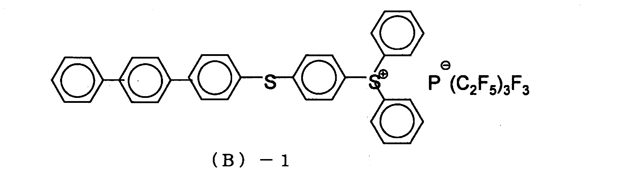
具体的には、下記式(A)-1で表されるポリマー(Mw=40000)を100質量部、下記式(B)-1で表される光酸発生剤((4-ターフェニルチオフェニル)ジフェニルスルフォニウム トリス(ペンタフルオロエチル)トリフルオロフォスフェート)を2.5質量部、下記式(C)-1で表される架橋剤を150質量部、及びPGMEAを34150質量部混合し、溶解してネガ型レジスト組成物溶液(1%PGMEA溶液)を調製した。なお、式(A)-1中、( )の右下の数値は各構成単位の割合(モル%)を示す。


ブロックコポリマーを溶解させる有機溶媒の種類が、現像処理に与える影響を調べた。
シリコン基板を硫酸/過酸化水素水混合液(体積比7:3)に1時間浸漬させた後、当該基板を水洗し、窒素ガスによって風乾した。次いで、当該基板表面に、製造例1により製造されたネガ型レジスト組成物溶液をスピンコート(回転数:2000rpm、60秒間)した後、250℃で60秒間加熱した。当該基板を、トルエンに30秒間浸漬させる処理を1回行い、窒素ガスによって風乾した。
UV露光量が、現像処理に与える影響を調べた。
シリコン基板を硫酸/過酸化水素水混合液(体積比7:3)に1時間浸漬させた後、当該基板を水洗し、窒素ガスによって風乾した。次いで、当該基板表面に、製造例1により製造されたネガ型レジスト組成物溶液を実施例2と同様にして塗布し、風乾した。
次いで、オゾンレス低圧水銀ランプ(254nm)(セン特殊光源社製)を用いて、当該基板に0、5、10、15、又は30分間UVを照射した。356nm用の照度測定計で測定したところ、UV照度は18.4mW/cm2であったため、UV露光量はそれぞれ、365nmでの露光量として0、5.5、11.0、16.5、及び33.1mJ/cm2であると算出された。その後、PGMEAにそれぞれ1分間浸漬させた後、さらに当該基板を窒素ガスで風乾した。
ブロックコポリマーを含む層を形成する前にガイドパターンが形成された基板を用いるグラフォエピタキシープロセスにて、ナノ構造体を表面に備える基板を製造した。
まず、シリコン基板に、スピンコートによって有機系反射防止膜組成物「ARC29A」(商品名、ブリュワーサイエンス社製)を膜厚82nmになるように製膜し、205℃で60秒加熱した。次に、スピンコートによってSM-008T(商品名、東京応化工業社製)を膜厚1nmになるように製膜し、250℃で600秒間加熱した。
次いで、当該基板表面に、SG-N002 PM(商品名、東京応化工業社製)を、スピンナーを用いて塗布し、ホットプレート上で、85℃、60秒間の条件でプレベーク(PAB)処理を行い、乾燥することにより、膜厚100nmのガイドパターン形成用レジスト膜を形成した。
当該ガイドパターン形成用レジスト膜に対して、露光装置S-302(ニコン社製;NA(開口数)=0.60、σ=2/3)により、マスクパターンを介して選択的に露光した(露光量=17.5mJ/cm2)。露光後、酢酸ブチルで16秒間の条件で現像し、その後100℃、60秒間、次いで200℃で300秒間の条件でポストベーク処理を行った後、その結果、ガイドパターンとして、ライン幅160nm、スペース間隔160nmのL/Sパターンが形成された。
オゾンレス低圧水銀ランプ(254nm)(セン特殊光源社製)を用いて、当該基板に対して、UV露光量が36mJ/cm2となるように、窒素気流下、UVを照射した。その後、当該基板をPGMEAに1分間浸漬させた後、窒素ガスで風乾した。
シリコン基板を硫酸/過酸化水素水混合液(体積比7:3)に1時間浸漬させた後、当該基板を水洗し、窒素ガスによって風乾した。次いで、当該基板の表面に、フェネチルトリクロロシランのトルエン溶液(1.0体積%)を滴下し、回転塗布した。その後、当該基板を250℃で60秒間加熱し、最後にトルエンに30秒間浸漬後、窒素ガスで風乾した。
この基板に、PS-PMMAブロックコポリマー1(PSの分子量:53000、PMMAの分子量:54000、分散度(Poly dispersity index:PDI):1.16)のトルエン溶液(17.5mg/ml)をスピンコート(回転数:3000rpm、60秒間)した。PS-PMMAブロックコポリマーが塗布された基板を、窒素気流下、200℃で1時間加熱させて相分離構造を形成させた。
次いで、オゾンレス低圧水銀ランプ(254nm)(セン特殊光源社製)を用いて、当該基板に30分間UVを照射した。356nm用の照度測定計で測定したところ、UV照度は16.2mW/cm2であったため、UV露光量は29.1mJ/cm2であると算出された。その後、トルエン(特級)又はベンゼンにそれぞれ1分間浸漬させた後、さらに当該基板を窒素ガスで風乾した。これにより、当該基板上には、表面がPSからなる相のみからなるナノ構造体が残存した。なお、UV照射から窒素ガス風乾までを現像処理という。
現像処理後の表面を走査型電子顕微鏡で観察した。この結果、現像液としてトルエン及びベンゼンのいずれを用いた場合でも、相分離構造を反映したナノ構造体が観察された。
シリコン基板を硫酸/過酸化水素水混合液(体積比7:3)に1時間浸漬させた後、当該基板を水洗し、窒素ガスによって風乾した。次いで、当該基板の表面に、フェネチルトリクロロシランのトルエン溶液(1.0体積%)を滴下し、回転塗布した。その後、当該基板を250℃で60秒間加熱し、最後にトルエンに30秒間浸漬後、窒素ガスで風乾した。
次いで、当該基板表面に、PS-PMMAブロックコポリマー2(PSの分子量:18000、PMMAの分子量:18000、分散度:1.06)のトルエン溶液(17.5mg/ml)をスピンコート(回転数:3000rpm、60秒間)し、110℃、90秒間プレベーク(PAB)処理を行い、膜厚50~60nmのPS-PMMAブロックコポリマー層を形成した。PS-PMMAブロックコポリマー層が形成された基板を、窒素気流下、200℃で1時間加熱させて相分離構造を形成させた。
オゾンレス低圧水銀ランプ(254nm)(セン特殊光源社製)を用いて、当該基板に対して、UV露光量が15mJ/cm2となるように、窒素気流下、UVを照射した。その後、当該基板をトルエン(特級)に1分間浸漬させた後、窒素ガスで風乾した。
ブロックコポリマーを含む層を形成する前にガイドパターンが形成された基板を用いるグラフォエピタキシープロセスにて、ナノ構造体を表面に備える基板を製造した。
まず、シリコン基板を硫酸/過酸化水素水混合液(体積比7:3)に1時間浸漬させた後、当該基板を水洗し、窒素ガスによって風乾した。次いで、当該基板の表面に、フェネチルトリクロロシランのトルエン溶液(1.0体積%)を滴下し、回転塗布した。その後、当該基板を250℃で60秒間加熱し、最後にトルエンに30秒間浸漬後、窒素ガスで風乾した。
次いで、当該基板表面に、TSMR-iN027(商品名、東京応化工業社製)を、スピンナーを用いて塗布し、ホットプレート上で、90℃、60秒間の条件でプレベーク(PAB)処理を行い、乾燥することにより、膜厚350nmのガイドパターン形成用レジスト膜を形成した。
当該ガイドパターン形成用レジスト膜に対して、i線露光装置NSR-2205i14E(ニコン社製;NA(開口数)=0.57、σ=0.56)により、マスクパターン(6%ハーフトーン)を介して選択的に、高圧水銀灯(365nm)を170m秒間照射した(露光量=85mJ/cm2)。そして、120℃、60秒間の条件で露光後加熱(PEB)処理を行い、さらに23℃にて2.38質量%TMAH水溶液(商品名:NMD-3、東京応化工業社製)で60秒間の条件で現像し、その後100℃、60秒間ポストベーク処理後、ghi線ブロードバンド露光機HMW-532D(ORC社製)によりマスクを介さずウエハー全面に紫外線を500mJ/cm2照射し、次いで130℃、5分間、その後200℃、5分間の条件でポストベーク処理を行った。その結果、ガイドパターンとして、ライン幅500nm、スペース間隔250nmのL/Sパターンが形成された。
オゾンレス低圧水銀ランプ(254nm)(セン特殊光源社製)を用いて、当該基板に対して、UV露光量が36mJ/cm2となるように、窒素気流下、UVを照射した。その後、当該基板をトルエン(特級)に3分間浸漬させた後、窒素ガスで風乾した。
ガイドパターン形成用レジスト膜に対するポストベーク処理を130℃、5分間の条件で行い、ガイドパターンとして、ライン幅350nm、スペース間隔350nmのL/Sパターンを形成し、PS-PMMAブロックコポリマー1のトルエン溶液に代えてPS-PMMAブロックコポリマー3(PSの分子量:37000、PMMAの分子量:37000、分散度:1.08)のトルエン溶液(17.5mg/ml)を用いた以外は、実施例7と同様にして、シリコン基板上にガイドパターンを形成後、当該基板上にPS-PMMAブロックコポリマー層を形成した後、相分離構造を形成した。
オゾンレス低圧水銀ランプ(254nm)(セン特殊光源社製)を用いて、当該基板に対して、UV露光量が36mJ/cm2となるように、窒素気流下、UVを照射した。その後、当該基板をトルエン(特級)に5分間浸漬させた後、窒素ガスで風乾した。
ガイドパターン形成用レジスト膜に対するポストベーク処理を200℃、5分間の条件で行い、ガイドパターンとして、ライン幅350nm、スペース間隔350nmのL/Sパターンを形成し、PS-PMMAブロックコポリマー1のトルエン溶液に代えて、実施例6で用いたPS-PMMAブロックコポリマー2のトルエン溶液を用いた以外は、実施例7と同様にして、シリコン基板上にガイドパターンを形成後、当該基板上にPS-PMMAブロックコポリマー層を形成した後、相分離構造を形成した。
オゾンレス低圧水銀ランプ(254nm)(セン特殊光源社製)を用いて、当該基板に対して、UV露光量が30mJ/cm2となるように、窒素気流下、UVを照射した。その後、当該基板をトルエン(特級)に10分間浸漬させた後、窒素ガスで風乾した。
ガイドパターンとして、L/Sパターンに代えて、ホール径310nm、ピッチ間隔980nmのホールレジストパターンを形成した以外は、実施例9と同様にして、シリコン基板上にガイドパターンを形成後、当該基板上にPS-PMMAブロックコポリマー層を形成し、相分離構造を形成した後、現像処理を行った。
現像処理後の基板表面を走査型電子顕微鏡で観察したところ、当該基板上には、ガイドパターンからなる鋳型ホール内に、相分離構造を反映した当該鋳型ホールと同心円状のシリンダー状のナノ構造体が形成されていた。
ブロックコポリマーを含む層を形成する前にガイドパターンが形成された基板を用いるグラフォエピタキシープロセスにて、ナノ構造体を表面に備える基板を製造した。
まず、シリコン基板に、スピンコートによって有機系反射防止膜組成物「ARC29A」(商品名、ブリュワーサイエンス社製)を膜厚82nmになるように製膜し、205℃で60秒加熱した。次に、スピンコートによってSM-008T(商品名、東京応化社製)を膜厚1nmになるように製膜し、250℃で600秒間加熱した。
次いで、当該基板表面に、SG-N002 PM(商品名、東京応化工業社製)を、スピンナーを用いて塗布し、ホットプレート上で、85℃、60秒間の条件でプレベーク(PAB)処理を行い、乾燥することにより、膜厚100nmのガイドパターン形成用レジスト膜を形成した。
当該ガイドパターン形成用レジスト膜に対して、露光装置S-308F(ニコン社製;NA(開口数)=0.92、Crosspole(0.76-0.95)with POLANO)により、マスクパターンを介して選択的に露光した(露光量=11mJ/cm2)。露光後、酢酸ブチルで16秒間の条件で現像し、その後100℃、60秒間、次いで200℃で300秒間の条件でポストベーク処理を行った後、その結果、ガイドパターンとして、ホール径85nm、ピッチ間隔158nmのホールレジストパターンが形成された。
ArF露光装置S-308F(193nm)(ニコン社製)を用いて、当該基板に対して、ArF露光量が400~4000mJ/cm2となるように、空気雰囲気下、ArFエキシマレーザーを照射した。その後、当該基板をトルエンに1分間浸漬させた後、窒素ガスで風乾した。
現像処理後の基板表面を走査型電子顕微鏡で観察したところ、当該基板上には、ガイドパターンからなる鋳型ホール内に、相分離構造を反映した当該鋳型ホールと同心円状のシリンダー状のナノ構造体が形成されていた。
現像液をトルエンに代えて、酢酸ブチルを用いた以外は実施例11と同様にして、シリコン基板上にガイドパターンを形成後、当該基盤上にブロックコポリマー層を形成し、相分離構造を形成した後、現像処理を行った。
現像処理後の基板表面を走査型電子顕微鏡で観察したところ、当該基板上には、ガイドパターンからなる鋳型ホール内に、相分離構造を反映した当該鋳型ホールと同心円状のシリンダー状のナノ構造体が形成されていた。
現像液をトルエンに代えて、2-ヘプタノンを用いた以外は実施例11と同様にして、シリコン基板上にガイドパターンを形成後、当該基盤上にブロックコポリマー層を形成し、相分離構造を形成した後、現像処理を行った。
現像処理後の基板表面を走査型電子顕微鏡で観察したところ、当該基板上には、ガイドパターンからなる鋳型ホール内に、相分離構造を反映した当該鋳型ホールと同心円状のシリンダー状のナノ構造体が形成されていた。
Claims (10)
- 複数種類のブロックが結合したブロックコポリマーを含む層を基板上に形成した後、当該層を加熱し、当該層を相分離させる相分離工程と、
前記層のうち、前記ブロックコポリマーを構成する複数種類のブロックのうちの少なくとも一種類のブロックからなる相の少なくとも一部を分解する分解工程と、
前記層を現像液に浸漬させ、前記分解工程において分解されたブロックを含む相を選択的に除去する選択的除去工程と、
を有し、
前記現像液が、SP値が7.5~11.5(cal/cm3)1/2であり、かつ25℃における蒸気圧が2.1kPa未満である有機溶媒、又はアルキル基、アルコキシ基、ハロゲン原子で置換されていても良いベンゼンを主成分とすることを特徴とする、ナノ構造体を表面に備える基板の製造方法。 - 前記現像液が、酢酸ブチル、2-ヘプタノン、及びプロピレングリコールモノメチルエーテルアセテートからなる群より選択される1種以上を含む請求項1に記載のナノ構造体を表面に備える基板の製造方法。
- 前記現像液が、ベンゼン、トルエン、エチルベンゼン、キシレン、アニソール、及びクロロベンゼンからなる群より選択される1種以上を含む請求項1に記載のナノ構造体を表面に備える基板の製造方法。
- 前記分解工程を、前記層に対して紫外線を照射することにより行う請求項1に記載のナノ構造体を表面に備える基板の製造方法。
- 前記層に対して、波長254nmにおける紫外線露光量が1~100mJ/cm2である請求項4に記載のナノ構造体を表面に備える基板の製造方法。
- 前記分解工程を、前記層に対してArFエキシマレーザーを照射することにより行う請求項1に記載のナノ構造体を表面に備える基板の製造方法。
- 前記層に対して、波長193nmにおけるArF露光量が400~4000mJ/cm2である請求項6に記載のナノ構造体を表面に備える基板の製造方法。
- 前記ブロックコポリマーが、ポリスチレンとポリメチルメタクリレートからなる請求項1に記載のナノ構造体を表面に備える基板の製造方法。
- 前記選択的除去工程により、前記基板表面の一部が露出し、
前記選択的除去工程後、さらに、
露出された基板表面に金属イオンを接触させ、基板表面と金属イオンとの間に起こる電気化学反応により、当該基板表面に金属を析出させる析出工程と、
を有する請求項1~8のいずれか一項に記載のナノ構造体を表面に備える基板の製造方法。 - 前記選択的除去工程後、さらに、
前記層の表面に、金属薄膜を形成する薄膜形成工程と、
前記金属薄膜の一部または全部を残したまま、前記層の一部または全部を除去する除去工程と、を有する請求項1~8のいずれか一項に記載のナノ構造体を表面に備える基板の製造方法。
Priority Applications (2)
| Application Number | Priority Date | Filing Date | Title |
|---|---|---|---|
| JP2012557987A JP6090777B2 (ja) | 2011-02-15 | 2012-02-15 | ナノ構造体を表面に備える基板の製造方法 |
| US13/984,405 US9060415B2 (en) | 2011-02-15 | 2012-02-15 | Method for producing substrate having surface nanostructure |
Applications Claiming Priority (6)
| Application Number | Priority Date | Filing Date | Title |
|---|---|---|---|
| JP2011-030274 | 2011-02-15 | ||
| JP2011030274 | 2011-02-15 | ||
| JP2011-198765 | 2011-09-12 | ||
| JP2011198765 | 2011-09-12 | ||
| JP2011198764 | 2011-09-12 | ||
| JP2011-198764 | 2011-09-12 |
Publications (1)
| Publication Number | Publication Date |
|---|---|
| WO2012111694A1 true WO2012111694A1 (ja) | 2012-08-23 |
Family
ID=46672609
Family Applications (1)
| Application Number | Title | Priority Date | Filing Date |
|---|---|---|---|
| PCT/JP2012/053499 Ceased WO2012111694A1 (ja) | 2011-02-15 | 2012-02-15 | ナノ構造体を表面に備える基板の製造方法 |
Country Status (4)
| Country | Link |
|---|---|
| US (1) | US9060415B2 (ja) |
| JP (1) | JP6090777B2 (ja) |
| TW (1) | TWI534072B (ja) |
| WO (1) | WO2012111694A1 (ja) |
Cited By (10)
| Publication number | Priority date | Publication date | Assignee | Title |
|---|---|---|---|---|
| WO2013146715A1 (ja) * | 2012-03-30 | 2013-10-03 | Jsr株式会社 | パターン形成方法 |
| WO2013150955A1 (ja) * | 2012-04-06 | 2013-10-10 | 東京エレクトロン株式会社 | パターン形成方法、パターン形成装置、及びコンピュータ可読記憶媒体 |
| WO2013161605A1 (ja) * | 2012-04-24 | 2013-10-31 | 東京エレクトロン株式会社 | パターン形成方法、パターン形成装置、及び非一時的なコンピュータ読み取り可能な記憶媒体 |
| JP2014011245A (ja) * | 2012-06-28 | 2014-01-20 | Institute Of Physical & Chemical Research | 微細パターン形成方法、現像液 |
| WO2014098025A1 (ja) * | 2012-12-18 | 2014-06-26 | 日産化学工業株式会社 | スチレン構造を含む自己組織化膜の下層膜形成組成物 |
| WO2014208311A1 (ja) * | 2013-06-26 | 2014-12-31 | 東京エレクトロン株式会社 | 基板処理方法、コンピュータ記憶媒体及び基板処理システム |
| WO2015075833A1 (ja) * | 2013-11-25 | 2015-05-28 | 東京エレクトロン株式会社 | パターン形成方法及び加熱装置 |
| JP2015144262A (ja) * | 2013-12-26 | 2015-08-06 | Jsr株式会社 | 下地膜形成用組成物及び自己組織化リソグラフィープロセス |
| JP2016516288A (ja) * | 2012-12-21 | 2016-06-02 | アルケマ フランス | ナノリソグラフィーマスクの製造方法 |
| JP2016209826A (ja) * | 2015-05-11 | 2016-12-15 | 東京応化工業株式会社 | 相分離構造を含む構造体の製造方法、ブロックコポリマー組成物及びブロックコポリマー組成物に用いる有機溶剤 |
Families Citing this family (8)
| Publication number | Priority date | Publication date | Assignee | Title |
|---|---|---|---|---|
| KR101529646B1 (ko) * | 2012-09-10 | 2015-06-17 | 주식회사 엘지화학 | 실리콘 옥사이드의 나노 패턴 형성 방법, 금속 나노 패턴의 형성 방법 및 이를 이용한 정보저장용 자기 기록 매체 |
| CN106104754B (zh) * | 2014-01-16 | 2020-07-28 | 布鲁尔科技公司 | 用于直接自组装的高chi嵌段共聚物 |
| JP2016058620A (ja) * | 2014-09-11 | 2016-04-21 | 株式会社東芝 | 半導体装置の製造方法 |
| JP1618421S (ja) | 2018-01-10 | 2018-11-19 | ||
| JP1618619S (ja) | 2018-01-10 | 2018-11-19 | ||
| USD928279S1 (en) | 2018-01-10 | 2021-08-17 | Kubota Corporation | Membrane cartridge for submerged membrane separation |
| EP3528045A1 (en) | 2018-02-16 | 2019-08-21 | IMEC vzw | Method for forming a cross-linked layer |
| US12521937B2 (en) * | 2021-03-23 | 2026-01-13 | Xerox Corporation | Piezoelectric composite filaments and use thereof in additive manufacturing |
Citations (3)
| Publication number | Priority date | Publication date | Assignee | Title |
|---|---|---|---|---|
| JP2007297644A (ja) * | 1999-06-07 | 2007-11-15 | Toshiba Corp | 多孔質構造体の製造方法 |
| JP2009138014A (ja) * | 2007-12-03 | 2009-06-25 | Toyota Central R&D Labs Inc | ナノ構造材料の製造方法 |
| JP2011126000A (ja) * | 2009-12-18 | 2011-06-30 | Hitachi Global Storage Technologies Netherlands Bv | ナノメートルスケールの自己組織化膜上の支持メンブラン |
Family Cites Families (5)
| Publication number | Priority date | Publication date | Assignee | Title |
|---|---|---|---|---|
| JP3940546B2 (ja) | 1999-06-07 | 2007-07-04 | 株式会社東芝 | パターン形成方法およびパターン形成材料 |
| JP4127682B2 (ja) | 1999-06-07 | 2008-07-30 | 株式会社東芝 | パターン形成方法 |
| JP4673266B2 (ja) | 2006-08-03 | 2011-04-20 | 日本電信電話株式会社 | パターン形成方法及びモールド |
| JP2009057518A (ja) | 2007-09-03 | 2009-03-19 | Institute Of Physical & Chemical Research | 異方性フィルムおよび異方性フィルムの製造方法 |
| JP2009297837A (ja) | 2008-06-13 | 2009-12-24 | Institute Of Physical & Chemical Research | ナノ構造体含有フィルムの製造方法およびナノ構造体含有フィルム |
-
2012
- 2012-02-15 WO PCT/JP2012/053499 patent/WO2012111694A1/ja not_active Ceased
- 2012-02-15 TW TW101104920A patent/TWI534072B/zh active
- 2012-02-15 JP JP2012557987A patent/JP6090777B2/ja active Active
- 2012-02-15 US US13/984,405 patent/US9060415B2/en active Active
Patent Citations (3)
| Publication number | Priority date | Publication date | Assignee | Title |
|---|---|---|---|---|
| JP2007297644A (ja) * | 1999-06-07 | 2007-11-15 | Toshiba Corp | 多孔質構造体の製造方法 |
| JP2009138014A (ja) * | 2007-12-03 | 2009-06-25 | Toyota Central R&D Labs Inc | ナノ構造材料の製造方法 |
| JP2011126000A (ja) * | 2009-12-18 | 2011-06-30 | Hitachi Global Storage Technologies Netherlands Bv | ナノメートルスケールの自己組織化膜上の支持メンブラン |
Cited By (22)
| Publication number | Priority date | Publication date | Assignee | Title |
|---|---|---|---|---|
| WO2013146715A1 (ja) * | 2012-03-30 | 2013-10-03 | Jsr株式会社 | パターン形成方法 |
| US20150062545A1 (en) * | 2012-04-06 | 2015-03-05 | Tokyo Electron Limited | Pattern forming method, pattern forming apparatus, and computer readable storage medium |
| WO2013150955A1 (ja) * | 2012-04-06 | 2013-10-10 | 東京エレクトロン株式会社 | パターン形成方法、パターン形成装置、及びコンピュータ可読記憶媒体 |
| JP2013232621A (ja) * | 2012-04-06 | 2013-11-14 | Tokyo Electron Ltd | パターン形成方法、パターン形成装置、及びコンピュータ可読記憶媒体 |
| KR101857323B1 (ko) | 2012-04-06 | 2018-05-11 | 도쿄엘렉트론가부시키가이샤 | 패턴 형성 방법, 패턴 형성 장치 및 컴퓨터 판독 가능 기억 매체 |
| US9618849B2 (en) | 2012-04-06 | 2017-04-11 | Tokyo Electron Limited | Pattern forming method, pattern forming apparatus, and computer readable storage medium |
| WO2013161605A1 (ja) * | 2012-04-24 | 2013-10-31 | 東京エレクトロン株式会社 | パターン形成方法、パターン形成装置、及び非一時的なコンピュータ読み取り可能な記憶媒体 |
| JP2013228492A (ja) * | 2012-04-24 | 2013-11-07 | Tokyo Electron Ltd | パターン形成方法、パターン形成装置、及びコンピュータ可読記憶媒体 |
| US9530645B2 (en) | 2012-04-24 | 2016-12-27 | Tokyo Electron Limited | Pattern forming method, pattern forming apparatus, and non-transitory computer-readable storage medium |
| JP2014011245A (ja) * | 2012-06-28 | 2014-01-20 | Institute Of Physical & Chemical Research | 微細パターン形成方法、現像液 |
| KR20150096668A (ko) * | 2012-12-18 | 2015-08-25 | 닛산 가가쿠 고교 가부시키 가이샤 | 스티렌구조를 포함하는 자기조직화막의 하층막 형성조성물 |
| JPWO2014098025A1 (ja) * | 2012-12-18 | 2017-01-12 | 日産化学工業株式会社 | スチレン構造を含む自己組織化膜の下層膜形成組成物 |
| WO2014098025A1 (ja) * | 2012-12-18 | 2014-06-26 | 日産化学工業株式会社 | スチレン構造を含む自己組織化膜の下層膜形成組成物 |
| US10280328B2 (en) | 2012-12-18 | 2019-05-07 | Nissan Chemical Industries, Ltd. | Bottom layer film-forming composition of self-organizing film containing styrene structure |
| KR102126789B1 (ko) * | 2012-12-18 | 2020-06-25 | 닛산 가가쿠 가부시키가이샤 | 스티렌구조를 포함하는 자기조직화막의 하층막 형성조성물 |
| JP2016516288A (ja) * | 2012-12-21 | 2016-06-02 | アルケマ フランス | ナノリソグラフィーマスクの製造方法 |
| JP2015008246A (ja) * | 2013-06-26 | 2015-01-15 | 東京エレクトロン株式会社 | 基板処理方法、プログラム、コンピュータ記憶媒体及び基板処理システム |
| WO2014208311A1 (ja) * | 2013-06-26 | 2014-12-31 | 東京エレクトロン株式会社 | 基板処理方法、コンピュータ記憶媒体及び基板処理システム |
| US9810987B2 (en) | 2013-06-26 | 2017-11-07 | Tokyo Electron Limited | Substrate treatment method, computer storage medium and substrate treatment system |
| WO2015075833A1 (ja) * | 2013-11-25 | 2015-05-28 | 東京エレクトロン株式会社 | パターン形成方法及び加熱装置 |
| JP2015144262A (ja) * | 2013-12-26 | 2015-08-06 | Jsr株式会社 | 下地膜形成用組成物及び自己組織化リソグラフィープロセス |
| JP2016209826A (ja) * | 2015-05-11 | 2016-12-15 | 東京応化工業株式会社 | 相分離構造を含む構造体の製造方法、ブロックコポリマー組成物及びブロックコポリマー組成物に用いる有機溶剤 |
Also Published As
| Publication number | Publication date |
|---|---|
| US20130313223A1 (en) | 2013-11-28 |
| JP6090777B2 (ja) | 2017-03-08 |
| TWI534072B (zh) | 2016-05-21 |
| TW201247521A (en) | 2012-12-01 |
| JPWO2012111694A1 (ja) | 2014-07-07 |
| US9060415B2 (en) | 2015-06-16 |
Similar Documents
| Publication | Publication Date | Title |
|---|---|---|
| JP6090777B2 (ja) | ナノ構造体を表面に備える基板の製造方法 | |
| JP5979660B2 (ja) | コンタクトホールパターンの形成方法 | |
| JP5891075B2 (ja) | ブロックコポリマー含有組成物及びパターンの縮小方法 | |
| JP5846568B2 (ja) | 相分離構造を有する層を表面に備える基板の製造方法 | |
| CN108137313B (zh) | 用于嵌段共聚物自组装的组合物和方法 | |
| TWI531526B (zh) | 表面具備金屬奈米構造體之基板及其製造方法 | |
| JP5934565B2 (ja) | パターンの縮小方法、及び組成物 | |
| TWI655217B (zh) | 底劑、含相分離結構的結構體的製造方法 | |
| JP6249714B2 (ja) | 相分離構造を含む構造体の製造方法 | |
| JP6020991B2 (ja) | 微細パターン形成方法、現像液 | |
| JP7008403B2 (ja) | 相分離構造形成用樹脂組成物、及び、相分離構造を含む構造体の製造方法 | |
| WO2018062157A1 (ja) | 相分離構造を含む構造体の製造方法 | |
| JP2020090628A (ja) | 相分離構造形成用樹脂組成物及び相分離構造を含む構造体の製造方法 | |
| JP7018791B2 (ja) | 相分離構造を含む構造体の製造方法 | |
| WO2023048114A1 (ja) | 相分離構造形成用樹脂組成物、及び、相分離構造を含む構造体の製造方法 | |
| JP2012116967A (ja) | 高分子ナノ構造体を表面に備える基板及びその製造方法 | |
| JP2015033753A (ja) | 相分離構造を含む構造体の製造方法、相分離構造体及びブロックコポリマー組成物 |
Legal Events
| Date | Code | Title | Description |
|---|---|---|---|
| 121 | Ep: the epo has been informed by wipo that ep was designated in this application |
Ref document number: 12747012 Country of ref document: EP Kind code of ref document: A1 |
|
| ENP | Entry into the national phase |
Ref document number: 2012557987 Country of ref document: JP Kind code of ref document: A |
|
| WWE | Wipo information: entry into national phase |
Ref document number: 13984405 Country of ref document: US |
|
| NENP | Non-entry into the national phase |
Ref country code: DE |
|
| 122 | Ep: pct application non-entry in european phase |
Ref document number: 12747012 Country of ref document: EP Kind code of ref document: A1 |