WO2012102087A1 - 液晶表示装置 - Google Patents
液晶表示装置 Download PDFInfo
- Publication number
- WO2012102087A1 WO2012102087A1 PCT/JP2012/050450 JP2012050450W WO2012102087A1 WO 2012102087 A1 WO2012102087 A1 WO 2012102087A1 JP 2012050450 W JP2012050450 W JP 2012050450W WO 2012102087 A1 WO2012102087 A1 WO 2012102087A1
- Authority
- WO
- WIPO (PCT)
- Prior art keywords
- liquid crystal
- crystal display
- display device
- conductive
- display element
- Prior art date
Links
Images


Classifications
-
- G—PHYSICS
- G02—OPTICS
- G02F—OPTICAL DEVICES OR ARRANGEMENTS FOR THE CONTROL OF LIGHT BY MODIFICATION OF THE OPTICAL PROPERTIES OF THE MEDIA OF THE ELEMENTS INVOLVED THEREIN; NON-LINEAR OPTICS; FREQUENCY-CHANGING OF LIGHT; OPTICAL LOGIC ELEMENTS; OPTICAL ANALOGUE/DIGITAL CONVERTERS
- G02F1/00—Devices or arrangements for the control of the intensity, colour, phase, polarisation or direction of light arriving from an independent light source, e.g. switching, gating or modulating; Non-linear optics
- G02F1/01—Devices or arrangements for the control of the intensity, colour, phase, polarisation or direction of light arriving from an independent light source, e.g. switching, gating or modulating; Non-linear optics for the control of the intensity, phase, polarisation or colour
- G02F1/13—Devices or arrangements for the control of the intensity, colour, phase, polarisation or direction of light arriving from an independent light source, e.g. switching, gating or modulating; Non-linear optics for the control of the intensity, phase, polarisation or colour based on liquid crystals, e.g. single liquid crystal display cells
- G02F1/133—Constructional arrangements; Operation of liquid crystal cells; Circuit arrangements
- G02F1/1333—Constructional arrangements; Manufacturing methods
- G02F1/1345—Conductors connecting electrodes to cell terminals
-
- G—PHYSICS
- G02—OPTICS
- G02F—OPTICAL DEVICES OR ARRANGEMENTS FOR THE CONTROL OF LIGHT BY MODIFICATION OF THE OPTICAL PROPERTIES OF THE MEDIA OF THE ELEMENTS INVOLVED THEREIN; NON-LINEAR OPTICS; FREQUENCY-CHANGING OF LIGHT; OPTICAL LOGIC ELEMENTS; OPTICAL ANALOGUE/DIGITAL CONVERTERS
- G02F1/00—Devices or arrangements for the control of the intensity, colour, phase, polarisation or direction of light arriving from an independent light source, e.g. switching, gating or modulating; Non-linear optics
- G02F1/01—Devices or arrangements for the control of the intensity, colour, phase, polarisation or direction of light arriving from an independent light source, e.g. switching, gating or modulating; Non-linear optics for the control of the intensity, phase, polarisation or colour
- G02F1/13—Devices or arrangements for the control of the intensity, colour, phase, polarisation or direction of light arriving from an independent light source, e.g. switching, gating or modulating; Non-linear optics for the control of the intensity, phase, polarisation or colour based on liquid crystals, e.g. single liquid crystal display cells
- G02F1/133—Constructional arrangements; Operation of liquid crystal cells; Circuit arrangements
- G02F1/1333—Constructional arrangements; Manufacturing methods
- G02F1/133308—Support structures for LCD panels, e.g. frames or bezels
- G02F1/13332—Front frames
-
- G—PHYSICS
- G02—OPTICS
- G02F—OPTICAL DEVICES OR ARRANGEMENTS FOR THE CONTROL OF LIGHT BY MODIFICATION OF THE OPTICAL PROPERTIES OF THE MEDIA OF THE ELEMENTS INVOLVED THEREIN; NON-LINEAR OPTICS; FREQUENCY-CHANGING OF LIGHT; OPTICAL LOGIC ELEMENTS; OPTICAL ANALOGUE/DIGITAL CONVERTERS
- G02F1/00—Devices or arrangements for the control of the intensity, colour, phase, polarisation or direction of light arriving from an independent light source, e.g. switching, gating or modulating; Non-linear optics
- G02F1/01—Devices or arrangements for the control of the intensity, colour, phase, polarisation or direction of light arriving from an independent light source, e.g. switching, gating or modulating; Non-linear optics for the control of the intensity, phase, polarisation or colour
- G02F1/13—Devices or arrangements for the control of the intensity, colour, phase, polarisation or direction of light arriving from an independent light source, e.g. switching, gating or modulating; Non-linear optics for the control of the intensity, phase, polarisation or colour based on liquid crystals, e.g. single liquid crystal display cells
- G02F1/133—Constructional arrangements; Operation of liquid crystal cells; Circuit arrangements
- G02F1/1333—Constructional arrangements; Manufacturing methods
- G02F1/133308—Support structures for LCD panels, e.g. frames or bezels
- G02F1/133334—Electromagnetic shields
-
- G—PHYSICS
- G02—OPTICS
- G02F—OPTICAL DEVICES OR ARRANGEMENTS FOR THE CONTROL OF LIGHT BY MODIFICATION OF THE OPTICAL PROPERTIES OF THE MEDIA OF THE ELEMENTS INVOLVED THEREIN; NON-LINEAR OPTICS; FREQUENCY-CHANGING OF LIGHT; OPTICAL LOGIC ELEMENTS; OPTICAL ANALOGUE/DIGITAL CONVERTERS
- G02F1/00—Devices or arrangements for the control of the intensity, colour, phase, polarisation or direction of light arriving from an independent light source, e.g. switching, gating or modulating; Non-linear optics
- G02F1/01—Devices or arrangements for the control of the intensity, colour, phase, polarisation or direction of light arriving from an independent light source, e.g. switching, gating or modulating; Non-linear optics for the control of the intensity, phase, polarisation or colour
- G02F1/13—Devices or arrangements for the control of the intensity, colour, phase, polarisation or direction of light arriving from an independent light source, e.g. switching, gating or modulating; Non-linear optics for the control of the intensity, phase, polarisation or colour based on liquid crystals, e.g. single liquid crystal display cells
- G02F1/133—Constructional arrangements; Operation of liquid crystal cells; Circuit arrangements
- G02F1/1333—Constructional arrangements; Manufacturing methods
- G02F1/1343—Electrodes
- G02F1/134309—Electrodes characterised by their geometrical arrangement
- G02F1/134327—Segmented, e.g. alpha numeric display
-
- G—PHYSICS
- G02—OPTICS
- G02F—OPTICAL DEVICES OR ARRANGEMENTS FOR THE CONTROL OF LIGHT BY MODIFICATION OF THE OPTICAL PROPERTIES OF THE MEDIA OF THE ELEMENTS INVOLVED THEREIN; NON-LINEAR OPTICS; FREQUENCY-CHANGING OF LIGHT; OPTICAL LOGIC ELEMENTS; OPTICAL ANALOGUE/DIGITAL CONVERTERS
- G02F1/00—Devices or arrangements for the control of the intensity, colour, phase, polarisation or direction of light arriving from an independent light source, e.g. switching, gating or modulating; Non-linear optics
- G02F1/01—Devices or arrangements for the control of the intensity, colour, phase, polarisation or direction of light arriving from an independent light source, e.g. switching, gating or modulating; Non-linear optics for the control of the intensity, phase, polarisation or colour
- G02F1/13—Devices or arrangements for the control of the intensity, colour, phase, polarisation or direction of light arriving from an independent light source, e.g. switching, gating or modulating; Non-linear optics for the control of the intensity, phase, polarisation or colour based on liquid crystals, e.g. single liquid crystal display cells
- G02F1/133—Constructional arrangements; Operation of liquid crystal cells; Circuit arrangements
- G02F1/1333—Constructional arrangements; Manufacturing methods
- G02F1/1345—Conductors connecting electrodes to cell terminals
- G02F1/13458—Terminal pads
-
- G—PHYSICS
- G02—OPTICS
- G02F—OPTICAL DEVICES OR ARRANGEMENTS FOR THE CONTROL OF LIGHT BY MODIFICATION OF THE OPTICAL PROPERTIES OF THE MEDIA OF THE ELEMENTS INVOLVED THEREIN; NON-LINEAR OPTICS; FREQUENCY-CHANGING OF LIGHT; OPTICAL LOGIC ELEMENTS; OPTICAL ANALOGUE/DIGITAL CONVERTERS
- G02F2202/00—Materials and properties
- G02F2202/22—Antistatic materials or arrangements
Landscapes
- Physics & Mathematics (AREA)
- Nonlinear Science (AREA)
- Mathematical Physics (AREA)
- Chemical & Material Sciences (AREA)
- Crystallography & Structural Chemistry (AREA)
- General Physics & Mathematics (AREA)
- Optics & Photonics (AREA)
- Liquid Crystal (AREA)
- Devices For Indicating Variable Information By Combining Individual Elements (AREA)
Abstract
Description
そこで本発明は、前述の課題に対して対処するため、液晶表示素子が静電気の影響を受けて誤動作する虞のない液晶表示装置の提供を目的とするものである。
11 上側絶縁基板(絶縁基板)
11a 第1透明電極(透明電極)
12 下側絶縁基板(絶縁基板)
12a 第2透明電極(透明電極)
14 液晶
15 表示部
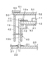
16 リード端子(接続部材)
17 導電部
18 第1のアース端子(第1のアース部)
18a、19a 挟持部
18b 接触片
18c 接続部
19 第2のアース端子(第2のアース部)
19b リード部
20 回路基板
21 接地部
40 ケース体
50 表示パネル(前面パネル)
51 透光性基板
53 透視部
60 見返し部材
T1 第1の導電パターン(導電部の所定箇所)
T2 第2の導電パターン
T3 第3の導電パターン
T4 第4の導電パターン
T5 第5の導電パターン
T6 第6の導電パターン
T7 第7の導電パターン(導電部の他の箇所)
Claims (4)
- 液晶を封止した一対の絶縁基板の内側表面に透明電極が各々設けられることで表示部を形成する液晶表示素子と、
所定の接続部材を介して前記液晶表示素子と導通接続される回路基板と、
前記透明電極を取り囲むように形成される導電部とを備え、
前記導電部が前記接続部材の配設位置を避けるように前記一対の絶縁基板のうちどちらか一方の絶縁基板に設けられている液晶表示装置において、
前記表示部を視認可能な透視部もしくは貫通部を有する前面パネルと、
一端側が前記導電部の所定箇所に導通接続されているとともに他端側が前記前面パネルに当接する第1のアース部と、
一端側が前記所定箇所とは異なる前記導電部の他の箇所に導通接続されているとともに他端側が前記回路基板に設けられた接地部に導通接続されている第2のアース部とを備えていることを特徴とする液晶表示装置。 - 前記接続部材は、前記液晶表示素子と前記回路基板とを導通接続するように前記一方の絶縁基板に設けられた複数個のリード端子からなり、
前記第1、第2のアース部は、前記リード端子と並設された状態で前記一方の絶縁基板に設けられた第1、第2のアース端子からなることを特徴とする請求項1記載の液晶表示装置。 - 前記第1のアース部の前記他端側は、バネ性を有した状態で前記前面パネルに当接していることを特徴とする請求項1または請求項2記載の液晶表示装置。
- 前記第1のアース部は、前記接地部に導通接続される接続部を備えていることを特徴とする請求項1から請求項3のうち何れか1つに記載の液晶表示装置。
Priority Applications (4)
| Application Number | Priority Date | Filing Date | Title |
|---|---|---|---|
| EP12739657.0A EP2669733B1 (en) | 2011-01-27 | 2012-01-12 | Liquid crystal display device |
| CN201280006300.XA CN103329031B (zh) | 2011-01-27 | 2012-01-12 | 液晶显示装置 |
| KR1020137018662A KR20140006824A (ko) | 2011-01-27 | 2012-01-12 | 액정표시장치 |
| US13/982,241 US9411202B2 (en) | 2011-01-27 | 2012-01-12 | Liquid crystal display device |
Applications Claiming Priority (2)
| Application Number | Priority Date | Filing Date | Title |
|---|---|---|---|
| JP2011-014975 | 2011-01-27 | ||
| JP2011014975A JP5590403B2 (ja) | 2011-01-27 | 2011-01-27 | 液晶表示装置 |
Publications (1)
| Publication Number | Publication Date |
|---|---|
| WO2012102087A1 true WO2012102087A1 (ja) | 2012-08-02 |
Family
ID=46580660
Family Applications (1)
| Application Number | Title | Priority Date | Filing Date |
|---|---|---|---|
| PCT/JP2012/050450 WO2012102087A1 (ja) | 2011-01-27 | 2012-01-12 | 液晶表示装置 |
Country Status (6)
| Country | Link |
|---|---|
| US (1) | US9411202B2 (ja) |
| EP (1) | EP2669733B1 (ja) |
| JP (1) | JP5590403B2 (ja) |
| KR (1) | KR20140006824A (ja) |
| CN (1) | CN103329031B (ja) |
| WO (1) | WO2012102087A1 (ja) |
Cited By (1)
| Publication number | Priority date | Publication date | Assignee | Title |
|---|---|---|---|---|
| EP2985751A1 (en) * | 2013-04-09 | 2016-02-17 | Nippon Seiki Co., Ltd. | Display device |
Families Citing this family (3)
| Publication number | Priority date | Publication date | Assignee | Title |
|---|---|---|---|---|
| JP6493750B2 (ja) * | 2015-04-22 | 2019-04-03 | 日本精機株式会社 | 計器装置 |
| JP6837103B2 (ja) * | 2019-08-08 | 2021-03-03 | 日本精機株式会社 | 車両用表示装置 |
| US11363745B1 (en) * | 2020-07-07 | 2022-06-14 | Waymo Llc | Housing for display electromagnetic shielding and electrostatic grounding |
Citations (6)
| Publication number | Priority date | Publication date | Assignee | Title |
|---|---|---|---|---|
| JPH11185991A (ja) * | 1997-12-25 | 1999-07-09 | Casio Comput Co Ltd | 電子機器 |
| JP2004233890A (ja) * | 2003-01-31 | 2004-08-19 | Optrex Corp | 液晶表示素子およびその除電方法 |
| JP2006139100A (ja) * | 2004-11-12 | 2006-06-01 | Matsushita Electric Ind Co Ltd | 通信端末 |
| JP2007328922A (ja) * | 2006-06-06 | 2007-12-20 | Sharp Corp | 電子機器 |
| WO2008029906A1 (fr) * | 2006-09-08 | 2008-03-13 | Kyocera Corporation | Appareil électronique et téléphone portatif |
| JP2008170812A (ja) | 2007-01-12 | 2008-07-24 | Matsushita Electric Works Ltd | 液晶表示素子 |
Family Cites Families (22)
| Publication number | Priority date | Publication date | Assignee | Title |
|---|---|---|---|---|
| JPS5622468A (en) * | 1979-08-01 | 1981-03-03 | Nissan Motor | Liquid crystal display unit |
| JP2916824B2 (ja) * | 1991-05-31 | 1999-07-05 | アルプス電気株式会社 | 液晶表示装置 |
| JPH07152019A (ja) * | 1993-11-30 | 1995-06-16 | Matsushita Electric Ind Co Ltd | 液晶表示装置 |
| TWI234674B (en) * | 1995-10-12 | 2005-06-21 | Hitachi Ltd | In-plane electric field LCD panel with structure for preventing electric charging |
| US6532053B2 (en) * | 1996-12-18 | 2003-03-11 | Hitachi, Ltd. | Transverse electric field system liquid crystal display device suitable for improving aperture ratio |
| JPH10282896A (ja) * | 1997-04-07 | 1998-10-23 | Mitsubishi Electric Corp | 表示装置 |
| JP2000181362A (ja) * | 1998-12-17 | 2000-06-30 | Alps Electric Co Ltd | 液晶表示装置 |
| JP3107078B2 (ja) * | 1999-02-26 | 2000-11-06 | 日本電気株式会社 | 液晶表示装置 |
| CN1126003C (zh) * | 1999-05-21 | 2003-10-29 | 时至准钟表股份有限公司 | 液晶显示面板 |
| JP2001147441A (ja) * | 1999-11-19 | 2001-05-29 | Nec Corp | 横電界液晶表示装置 |
| CN1292300C (zh) * | 2003-04-29 | 2006-12-27 | 明基电通股份有限公司 | 电子装置及其抗静电放电方法 |
| KR101107982B1 (ko) | 2004-08-19 | 2012-01-25 | 삼성전자주식회사 | 평판표시장치 |
| JP4892946B2 (ja) * | 2005-12-08 | 2012-03-07 | エプソンイメージングデバイス株式会社 | 電気光学装置及び電子機器 |
| US8400599B2 (en) * | 2006-08-16 | 2013-03-19 | Samsung Display Co., Ltd. | Liquid crystal display panel having a light blocking electrode |
| KR20080023466A (ko) * | 2006-09-11 | 2008-03-14 | 삼성에스디아이 주식회사 | 평판 표시 장치 |
| JP2009175709A (ja) * | 2007-12-27 | 2009-08-06 | Seiko Instruments Inc | 表示装置 |
| JP5283255B2 (ja) * | 2008-02-14 | 2013-09-04 | 株式会社ジャパンディスプレイ | 液晶表示装置 |
| TWI376544B (en) | 2008-06-16 | 2012-11-11 | Wintek Corp | Liquid crystal display panel |
| JP5311018B2 (ja) * | 2008-12-23 | 2013-10-09 | 日本精機株式会社 | 液晶表示装置 |
| JP5079715B2 (ja) * | 2009-01-16 | 2012-11-21 | 株式会社ジャパンディスプレイウェスト | 液晶表示装置 |
| JP5690178B2 (ja) * | 2010-04-26 | 2015-03-25 | 京セラディスプレイ株式会社 | 液晶表示装置 |
| KR20120097146A (ko) * | 2011-02-24 | 2012-09-03 | 엘지디스플레이 주식회사 | 액정표시장치 |
-
2011
- 2011-01-27 JP JP2011014975A patent/JP5590403B2/ja active Active
-
2012
- 2012-01-12 CN CN201280006300.XA patent/CN103329031B/zh not_active Expired - Fee Related
- 2012-01-12 EP EP12739657.0A patent/EP2669733B1/en not_active Not-in-force
- 2012-01-12 KR KR1020137018662A patent/KR20140006824A/ko not_active Application Discontinuation
- 2012-01-12 WO PCT/JP2012/050450 patent/WO2012102087A1/ja active Application Filing
- 2012-01-12 US US13/982,241 patent/US9411202B2/en active Active
Patent Citations (6)
| Publication number | Priority date | Publication date | Assignee | Title |
|---|---|---|---|---|
| JPH11185991A (ja) * | 1997-12-25 | 1999-07-09 | Casio Comput Co Ltd | 電子機器 |
| JP2004233890A (ja) * | 2003-01-31 | 2004-08-19 | Optrex Corp | 液晶表示素子およびその除電方法 |
| JP2006139100A (ja) * | 2004-11-12 | 2006-06-01 | Matsushita Electric Ind Co Ltd | 通信端末 |
| JP2007328922A (ja) * | 2006-06-06 | 2007-12-20 | Sharp Corp | 電子機器 |
| WO2008029906A1 (fr) * | 2006-09-08 | 2008-03-13 | Kyocera Corporation | Appareil électronique et téléphone portatif |
| JP2008170812A (ja) | 2007-01-12 | 2008-07-24 | Matsushita Electric Works Ltd | 液晶表示素子 |
Non-Patent Citations (1)
| Title |
|---|
| See also references of EP2669733A4 * |
Cited By (2)
| Publication number | Priority date | Publication date | Assignee | Title |
|---|---|---|---|---|
| EP2985751A1 (en) * | 2013-04-09 | 2016-02-17 | Nippon Seiki Co., Ltd. | Display device |
| EP2985751A4 (en) * | 2013-04-09 | 2017-05-03 | Nippon Seiki Co., Ltd. | Display device |
Also Published As
| Publication number | Publication date |
|---|---|
| KR20140006824A (ko) | 2014-01-16 |
| CN103329031B (zh) | 2016-01-20 |
| US20130314657A1 (en) | 2013-11-28 |
| EP2669733A1 (en) | 2013-12-04 |
| US9411202B2 (en) | 2016-08-09 |
| JP5590403B2 (ja) | 2014-09-17 |
| CN103329031A (zh) | 2013-09-25 |
| JP2012155176A (ja) | 2012-08-16 |
| EP2669733B1 (en) | 2017-06-28 |
| EP2669733A4 (en) | 2014-08-20 |
Similar Documents
| Publication | Publication Date | Title |
|---|---|---|
| JP5590403B2 (ja) | 液晶表示装置 | |
| JP5406007B2 (ja) | 計器装置 | |
| US20180239484A1 (en) | Touch sensitive cover plate and manufacturing method thereof, and touch sensitive display device | |
| JP2011059136A (ja) | 表示装置及び該表示装置を備えた車両用計器装置 | |
| JP5207135B2 (ja) | 計器装置 | |
| JP5621647B2 (ja) | 液晶表示装置 | |
| JP2014137458A (ja) | 表示装置 | |
| JP6048061B2 (ja) | 液晶表示装置 | |
| WO2018193953A1 (ja) | 表示装置 | |
| JP6493750B2 (ja) | 計器装置 | |
| EP3581996B1 (en) | Image display device | |
| JP2012153281A (ja) | 表示装置 | |
| JP2012189666A (ja) | 表示装置 | |
| JP5510391B2 (ja) | 電気回路装置 | |
| JP2016038443A (ja) | 車両用表示装置 | |
| JPH027071B2 (ja) | ||
| JP6790748B2 (ja) | 計器装置 | |
| JP5513812B2 (ja) | 表示装置 | |
| JP2015087138A (ja) | 車両用表示装置 | |
| JP2010151852A (ja) | 液晶表示装置 | |
| JP5609077B2 (ja) | 表示装置 | |
| JP2016008947A (ja) | 表示装置 | |
| JP2013235168A (ja) | 表示装置 | |
| WO2019022183A1 (ja) | 計器 | |
| JP2019002984A (ja) | 表示装置 |
Legal Events
| Date | Code | Title | Description |
|---|---|---|---|
| 121 | Ep: the epo has been informed by wipo that ep was designated in this application |
Ref document number: 12739657 Country of ref document: EP Kind code of ref document: A1 |
|
| REEP | Request for entry into the european phase |
Ref document number: 2012739657 Country of ref document: EP |
|
| WWE | Wipo information: entry into national phase |
Ref document number: 2012739657 Country of ref document: EP |
|
| ENP | Entry into the national phase |
Ref document number: 20137018662 Country of ref document: KR Kind code of ref document: A |
|
| WWE | Wipo information: entry into national phase |
Ref document number: 13982241 Country of ref document: US |
|
| NENP | Non-entry into the national phase |
Ref country code: DE |