WO2012090350A1 - Dispositif émetteur de lumière et lampe - Google Patents
Dispositif émetteur de lumière et lampe Download PDFInfo
- Publication number
- WO2012090350A1 WO2012090350A1 PCT/JP2011/004678 JP2011004678W WO2012090350A1 WO 2012090350 A1 WO2012090350 A1 WO 2012090350A1 JP 2011004678 W JP2011004678 W JP 2011004678W WO 2012090350 A1 WO2012090350 A1 WO 2012090350A1
- Authority
- WO
- WIPO (PCT)
- Prior art keywords
- light emitting
- emitting device
- light
- groove
- wavelength conversion
- Prior art date
Links
Images


Classifications
-
- H—ELECTRICITY
- H01—ELECTRIC ELEMENTS
- H01L—SEMICONDUCTOR DEVICES NOT COVERED BY CLASS H10
- H01L33/00—Semiconductor devices with at least one potential-jump barrier or surface barrier specially adapted for light emission; Processes or apparatus specially adapted for the manufacture or treatment thereof or of parts thereof; Details thereof
- H01L33/48—Semiconductor devices with at least one potential-jump barrier or surface barrier specially adapted for light emission; Processes or apparatus specially adapted for the manufacture or treatment thereof or of parts thereof; Details thereof characterised by the semiconductor body packages
- H01L33/50—Wavelength conversion elements
- H01L33/507—Wavelength conversion elements the elements being in intimate contact with parts other than the semiconductor body or integrated with parts other than the semiconductor body
-
- F—MECHANICAL ENGINEERING; LIGHTING; HEATING; WEAPONS; BLASTING
- F21—LIGHTING
- F21K—NON-ELECTRIC LIGHT SOURCES USING LUMINESCENCE; LIGHT SOURCES USING ELECTROCHEMILUMINESCENCE; LIGHT SOURCES USING CHARGES OF COMBUSTIBLE MATERIAL; LIGHT SOURCES USING SEMICONDUCTOR DEVICES AS LIGHT-GENERATING ELEMENTS; LIGHT SOURCES NOT OTHERWISE PROVIDED FOR
- F21K9/00—Light sources using semiconductor devices as light-generating elements, e.g. using light-emitting diodes [LED] or lasers
- F21K9/20—Light sources comprising attachment means
- F21K9/23—Retrofit light sources for lighting devices with a single fitting for each light source, e.g. for substitution of incandescent lamps with bayonet or threaded fittings
- F21K9/232—Retrofit light sources for lighting devices with a single fitting for each light source, e.g. for substitution of incandescent lamps with bayonet or threaded fittings specially adapted for generating an essentially omnidirectional light distribution, e.g. with a glass bulb
-
- F—MECHANICAL ENGINEERING; LIGHTING; HEATING; WEAPONS; BLASTING
- F21—LIGHTING
- F21V—FUNCTIONAL FEATURES OR DETAILS OF LIGHTING DEVICES OR SYSTEMS THEREOF; STRUCTURAL COMBINATIONS OF LIGHTING DEVICES WITH OTHER ARTICLES, NOT OTHERWISE PROVIDED FOR
- F21V3/00—Globes; Bowls; Cover glasses
-
- H—ELECTRICITY
- H01—ELECTRIC ELEMENTS
- H01L—SEMICONDUCTOR DEVICES NOT COVERED BY CLASS H10
- H01L33/00—Semiconductor devices with at least one potential-jump barrier or surface barrier specially adapted for light emission; Processes or apparatus specially adapted for the manufacture or treatment thereof or of parts thereof; Details thereof
- H01L33/48—Semiconductor devices with at least one potential-jump barrier or surface barrier specially adapted for light emission; Processes or apparatus specially adapted for the manufacture or treatment thereof or of parts thereof; Details thereof characterised by the semiconductor body packages
- H01L33/483—Containers
- H01L33/486—Containers adapted for surface mounting
-
- F—MECHANICAL ENGINEERING; LIGHTING; HEATING; WEAPONS; BLASTING
- F21—LIGHTING
- F21Y—INDEXING SCHEME ASSOCIATED WITH SUBCLASSES F21K, F21L, F21S and F21V, RELATING TO THE FORM OR THE KIND OF THE LIGHT SOURCES OR OF THE COLOUR OF THE LIGHT EMITTED
- F21Y2103/00—Elongate light sources, e.g. fluorescent tubes
- F21Y2103/10—Elongate light sources, e.g. fluorescent tubes comprising a linear array of point-like light-generating elements
-
- F—MECHANICAL ENGINEERING; LIGHTING; HEATING; WEAPONS; BLASTING
- F21—LIGHTING
- F21Y—INDEXING SCHEME ASSOCIATED WITH SUBCLASSES F21K, F21L, F21S and F21V, RELATING TO THE FORM OR THE KIND OF THE LIGHT SOURCES OR OF THE COLOUR OF THE LIGHT EMITTED
- F21Y2105/00—Planar light sources
- F21Y2105/10—Planar light sources comprising a two-dimensional array of point-like light-generating elements
-
- F—MECHANICAL ENGINEERING; LIGHTING; HEATING; WEAPONS; BLASTING
- F21—LIGHTING
- F21Y—INDEXING SCHEME ASSOCIATED WITH SUBCLASSES F21K, F21L, F21S and F21V, RELATING TO THE FORM OR THE KIND OF THE LIGHT SOURCES OR OF THE COLOUR OF THE LIGHT EMITTED
- F21Y2115/00—Light-generating elements of semiconductor light sources
- F21Y2115/10—Light-emitting diodes [LED]
-
- H—ELECTRICITY
- H01—ELECTRIC ELEMENTS
- H01L—SEMICONDUCTOR DEVICES NOT COVERED BY CLASS H10
- H01L25/00—Assemblies consisting of a plurality of individual semiconductor or other solid state devices ; Multistep manufacturing processes thereof
- H01L25/03—Assemblies consisting of a plurality of individual semiconductor or other solid state devices ; Multistep manufacturing processes thereof all the devices being of a type provided for in the same subgroup of groups H01L27/00 - H01L33/00, or in a single subclass of H10K, H10N, e.g. assemblies of rectifier diodes
- H01L25/04—Assemblies consisting of a plurality of individual semiconductor or other solid state devices ; Multistep manufacturing processes thereof all the devices being of a type provided for in the same subgroup of groups H01L27/00 - H01L33/00, or in a single subclass of H10K, H10N, e.g. assemblies of rectifier diodes the devices not having separate containers
- H01L25/075—Assemblies consisting of a plurality of individual semiconductor or other solid state devices ; Multistep manufacturing processes thereof all the devices being of a type provided for in the same subgroup of groups H01L27/00 - H01L33/00, or in a single subclass of H10K, H10N, e.g. assemblies of rectifier diodes the devices not having separate containers the devices being of a type provided for in group H01L33/00
- H01L25/0753—Assemblies consisting of a plurality of individual semiconductor or other solid state devices ; Multistep manufacturing processes thereof all the devices being of a type provided for in the same subgroup of groups H01L27/00 - H01L33/00, or in a single subclass of H10K, H10N, e.g. assemblies of rectifier diodes the devices not having separate containers the devices being of a type provided for in group H01L33/00 the devices being arranged next to each other
-
- H—ELECTRICITY
- H01—ELECTRIC ELEMENTS
- H01L—SEMICONDUCTOR DEVICES NOT COVERED BY CLASS H10
- H01L2924/00—Indexing scheme for arrangements or methods for connecting or disconnecting semiconductor or solid-state bodies as covered by H01L24/00
- H01L2924/0001—Technical content checked by a classifier
- H01L2924/0002—Not covered by any one of groups H01L24/00, H01L24/00 and H01L2224/00
-
- H—ELECTRICITY
- H01—ELECTRIC ELEMENTS
- H01L—SEMICONDUCTOR DEVICES NOT COVERED BY CLASS H10
- H01L33/00—Semiconductor devices with at least one potential-jump barrier or surface barrier specially adapted for light emission; Processes or apparatus specially adapted for the manufacture or treatment thereof or of parts thereof; Details thereof
- H01L33/48—Semiconductor devices with at least one potential-jump barrier or surface barrier specially adapted for light emission; Processes or apparatus specially adapted for the manufacture or treatment thereof or of parts thereof; Details thereof characterised by the semiconductor body packages
- H01L33/50—Wavelength conversion elements
- H01L33/505—Wavelength conversion elements characterised by the shape, e.g. plate or foil
-
- H—ELECTRICITY
- H01—ELECTRIC ELEMENTS
- H01L—SEMICONDUCTOR DEVICES NOT COVERED BY CLASS H10
- H01L33/00—Semiconductor devices with at least one potential-jump barrier or surface barrier specially adapted for light emission; Processes or apparatus specially adapted for the manufacture or treatment thereof or of parts thereof; Details thereof
- H01L33/48—Semiconductor devices with at least one potential-jump barrier or surface barrier specially adapted for light emission; Processes or apparatus specially adapted for the manufacture or treatment thereof or of parts thereof; Details thereof characterised by the semiconductor body packages
- H01L33/50—Wavelength conversion elements
- H01L33/508—Wavelength conversion elements having a non-uniform spatial arrangement or non-uniform concentration, e.g. patterned wavelength conversion layer, wavelength conversion layer with a concentration gradient of the wavelength conversion material
Definitions
- the present invention relates to a light emitting device including a semiconductor light emitting element, and a lamp including the light emitting device.
- LEDs Light Emitting Diodes
- an LED lamp there are a straight tube type LED lamp (straight tube type LED lamp) and a bulb-shaped LED lamp (bulb-shaped LED lamp). Also, in any of the lamps, an LED module (light emitting module) configured by mounting a plurality of LEDs on a substrate is used.
- Patent Document 1 discloses a conventional bulb-shaped LED lamp.
- Patent Document 2 discloses a conventional straight tube type LED lamp.
- a heat sink is used to dissipate the heat generated by the LED, and the LED module is fixed to the heat sink.
- a metal casing functioning as a heat sink is provided between the hemispherical glove and the cap, and the LED module is mounted and fixed on the upper surface of the metal casing It is done.
- a heat sink is used to dissipate the heat generated by the LED.
- a long metal base made of aluminum or the like is used as the heat sink.
- the metal base is fixed to the inner surface of the straight pipe by an adhesive, and the LED module is fixed to the upper surface of the metal base.
- the spread of light is different from that of an incandescent lamp, a compact fluorescent lamp, or a straight tubular fluorescent lamp having all light distribution characteristics.
- the configuration of the bulb-shaped LED lamp similar to that of the incandescent bulb. That is, a bulb-shaped LED lamp having a configuration in which the filament coil of the incandescent bulb is simply replaced with the LED module without using a heat sink can be considered. In this case, the light from the LED module is not blocked by the heat sink.
- the conventional LED module is configured to allow the light emitted from the LED module to travel to the side opposite to the heat sink without traveling to the heat sink side. That is, the conventional LED module is configured to emit light only from one side of the surface of the substrate on which the LED is mounted.
- the present invention has been made in consideration of the above-described conventional problems, and an object thereof is to provide a light emitting device and a lamp using a semiconductor light emitting element, which are light emitting characteristics having light distribution characteristics in multiple directions.
- a light emitting device is a light transmitting substrate, a semiconductor light emitting element disposed on the substrate, and a sealing member for sealing the semiconductor light emitting element.
- a sealing member including a first wavelength conversion material for converting a wavelength of light emitted by the semiconductor light emitting element into a predetermined wavelength, and a groove provided on a side of the semiconductor light emitting element, the substrate being A second wavelength which is provided in a recessed shape from a rear surface which is an arrangement surface on which the semiconductor light emitting device is arranged or a surface opposite to the arrangement surface, and which converts a wavelength of light emitted by the semiconductor light emitting device into the predetermined wavelength And a groove for receiving the conversion material.
- the light emitted from the semiconductor light emitting element is converted into a predetermined wavelength by the first wavelength conversion material contained in the sealing member and emitted to the outside. Further, the light emitted from the semiconductor light emitting element is converted to a predetermined wavelength by the second wavelength conversion material accommodated in the groove provided at the side position of the semiconductor light emitting element of the base and emitted to the outside.
- the semiconductor light emitting element is disposed on the upper surface of the base, light emitted from the semiconductor light emitting element is emitted as light of a predetermined wavelength toward at least the upper side and the side of the base.
- the second wavelength conversion material is accommodated in the groove, for example, the complication of the manufacturing process which occurs when applying the material containing the second wavelength conversion material on the side surface of the base, and the peeling of the material from the base It is hard to produce problems.
- a substrate having a thickness of about 1 mm is employed as the substrate, application of the material to the side surface is not easy and peeling is easy, so the configuration of the light emitting device of this embodiment is useful.
- the light emitting device of this embodiment is a light emitting device having light distribution characteristics in multiple directions and having high practicability.
- the grooves may be provided on both sides of the semiconductor light emitting element.
- the semiconductor light emitting device when the semiconductor light emitting device is disposed on the upper surface of the base, the light converted into the predetermined wavelength can be emitted toward at least the upper side of the base and the both sides.
- the groove may be provided to surround the semiconductor light emitting element.
- the first wavelength conversion material and the second wavelength conversion material are the same material, and the sealing member seals the semiconductor light emitting element.
- the second wavelength conversion material may be accommodated in the groove by entering into the groove.
- the sealing member covers the semiconductor light emitting element and continuously exists to the inside of the groove. That is, in the case of manufacturing the light emitting device of the present embodiment, for example, when applying the resin constituting the sealing member to the semiconductor light emitting element, the resin is poured into the groove to form the sealing member and to the groove. The placement of the second wavelength conversion material is performed. That is, a light emitting device having light distribution characteristics in multiple directions can be obtained by an efficient process.
- the light emitting device further includes a wavelength conversion unit that is disposed on the back surface of the base and includes a third wavelength conversion material that converts light emitted by the semiconductor light emitting element into the predetermined wavelength. It may be
- the semiconductor light emitting device when the semiconductor light emitting device is disposed on the upper surface of the base, the light converted into the predetermined wavelength can be emitted in all directions centered on the base, for example.
- the wavelength conversion unit is a sintered film formed on the back surface, and the sintered film is formed of the third wavelength conversion material and an inorganic material. And the binder for sintering.
- the durability of the wavelength conversion unit against heat and vibration can be improved.
- the first wavelength conversion material, the second wavelength conversion material, and the third wavelength conversion material are phosphors that emit light by being excited by light emitted from the semiconductor light emitting element. It may be composed of particles.
- the wavelength conversion materials used in different parts of the light emitting device are shared.
- the manufacture of the light emitting device can be streamlined, and the uniformity of the color of light emitted in multiple directions can be improved.
- a plurality of the semiconductor light emitting elements are disposed on the disposition surface of the base, and at least a part of the groove is an array of the plurality of semiconductor light emitting elements. It may extend along the direction.
- a lamp according to an aspect of the present invention includes the light emitting device according to any of the above aspects.
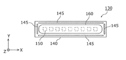
- FIG. 1 is an external perspective view of a light emitting device according to Embodiment 1 of the present invention.
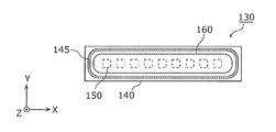
- FIG. 2 is a top view of the light emitting device in the first embodiment.
- FIG. 3 is a cross-sectional view showing an AA cross section in FIG.
- FIG. 4 is a cross-sectional view showing a cross section BB in FIG.
- FIG. 5 is a schematic view for explaining basic light distribution characteristics of the light emitting device according to the first embodiment.
- FIG. 6 is a cross-sectional view showing an outline of the configuration in the case where the light emitting device in Embodiment 1 has a wavelength conversion unit on the back surface.
- FIG. 1 is an external perspective view of a light emitting device according to Embodiment 1 of the present invention.
- FIG. 2 is a top view of the light emitting device in the first embodiment.
- FIG. 3 is a cross-sectional view showing an AA cross section in FIG.
- FIG. 4 is a cross-sectional view showing a
- FIG. 7 is a cross-sectional view showing an outline of the configuration when the light emitting device in the first embodiment is provided with a reflective film on the back surface.
- FIG. 8 is a cross-sectional view showing a configuration outline when the sealing member and the inward material of the groove are integrally provided in the light emitting device in the first embodiment.
- FIG. 9 is a first diagram showing another example of groove formation positions in the first embodiment.
- FIG. 10 is a second view showing another example of the formation position of the groove in the first embodiment.
- FIG. 11 is a third diagram showing another example of the groove formation position in the first embodiment.
- FIG. 12 is a fourth diagram showing another example of groove formation positions in the first embodiment.
- FIG. 13 is a first diagram showing another example of the overall shape of the groove in the first embodiment.
- FIG. 14 is a second diagram showing another example of the overall shape of the groove in the first embodiment.
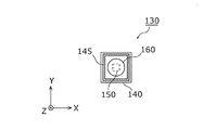
- FIG. 15 is a diagram showing a configuration outline when the light emitting device in the first embodiment includes only one LED.
- FIG. 16 is a diagram showing a configuration outline in the case where the light emitting device in the first embodiment is provided with a plurality of LED groups.
- FIG. 17 is a perspective view of a light bulb shaped lamp according to Embodiment 2 of the present invention.
- FIG. 18 is an exploded perspective view of the light bulb shaped lamp in the second embodiment.
- FIG. 19 is a front view of the light bulb shaped lamp in the second embodiment.
- Embodiment 1 First, a schematic configuration of the light emitting device in the first embodiment of the present invention will be described with reference to FIGS. 1 and 2.
- FIG. 1 a schematic configuration of the light emitting device in the first embodiment of the present invention will be described with reference to FIGS. 1 and 2.
- FIG. 1 a schematic configuration of the light emitting device in the first embodiment of the present invention will be described with reference to FIGS. 1 and 2.
- FIG. 1 is an external perspective view of light emitting device 130 in the first embodiment of the present invention
- FIG. 2 is a top view of light emitting device 130 in the first embodiment.
- the light emitting device 130 in the first embodiment of the present invention is an LED module that emits predetermined illumination light.
- the light emitting device 130 includes a light transmitting base 140, an LED 150 disposed on the base 140, a sealing member 160 for sealing the LED 150, and a groove 145 provided on the side of the LED 150.
- the base 140 is, for example, a substrate having a thickness of about 1 mm. Further, as such a substrate 140, a translucent ceramic substrate made of alumina or aluminum nitride, a transparent glass substrate, a substrate made of quartz, a sapphire substrate, or a resin substrate is employed.
- the LED 150 is an example of a semiconductor light emitting element. Further, in the present embodiment, the plurality of LEDs 150 are linearly arranged on the upper surface of the base 140. Further, the plurality of LEDs 150 are connected, for example, in series by wiring not shown, and emit light by supplying electricity through electrodes provided at both ends thereof.
- each of the LEDs 150 is a bare chip that emits monochromatic visible light, and is die-bonded onto the substrate 140 by a translucent die attach agent (die bonding agent).
- Each LED 150 is an LED chip that emits light in all directions, that is, side, upward and downward. For example, 20% of the total light amount laterally, 60% of the total light amount upward, and 20 of the total light amount downward Emits% light.
- each LED 150 for example, a blue LED chip that emits blue light is adopted.
- the blue LED chip for example, a gallium nitride based semiconductor light emitting element having a center wavelength of 440 nm to 470 nm, which is made of an InGaN based material, is used.
- the sealing member 160 collectively seals all the LEDs 150 on the base 140 and has a first wavelength conversion material that converts the wavelength of light emitted by the LEDs 150 into a predetermined wavelength.
- the sealing member 160 is a phosphor-containing resin in which predetermined phosphor particles are contained as a first wavelength conversion material in a predetermined resin.
- the sealing member 160 is, for example, a material in which predetermined phosphor particles are dispersed in a translucent material such as silicone resin.
- the groove 145 is a groove provided in a recessed shape from the arrangement surface of the base 140 on which the LED 150 is disposed.
- the second wavelength conversion material for converting the wavelength of the light emitted from the LED 150 into the predetermined wavelength is accommodated in the groove 145.
- the groove 145 is extended along the arrangement direction of the plurality of LEDs 150. More specifically, as shown in FIG. 2, the grooves 145 are arranged to surround all the LEDs 150. Also, focusing on a certain LED 150, grooves 145 are provided on at least both sides of the LED 150.
- FIG. 3 is a cross-sectional view showing an AA cross section in FIG. 2
- FIG. 4 is a cross-sectional view showing a BB cross section in FIG.
- the sealing member 160 includes the first wavelength conversion material 161, and the groove 145 contains the second wavelength conversion material 162.
- the groove 145 accommodates a phosphor-containing resin in which predetermined phosphor particles are contained as the second wavelength conversion material 162 in a predetermined resin.
- the light emitting device 130 of this embodiment has light distribution characteristics in multiple directions by having such a configuration.
- FIG. 5 is a schematic view for explaining the basic light distribution characteristic of the light emitting device 130 according to the first embodiment.
- the light emitted from the LED 150 is emitted upward through the sealing member 160 and emitted laterally across the groove 145.
- a blue LED is employed as the LED 150, and YAG (yttrium aluminum garnet) -based yellow phosphor particles are used as the first wavelength conversion material 161 and the second wavelength conversion material 162.
- YAG yttrium aluminum garnet
- the yellow phosphor particles emit yellow light when excited by the blue light from the LED 150. As a result, white light obtained by the yellow light and the blue light from the LED 150 is emitted.
- the blue light emitted by the LED 150 is wavelength-converted by the first wavelength conversion material 161, becomes white light, and is emitted upward (in the positive Z-axis direction).
- the blue light emitted from the LED 150 is converted by the second wavelength conversion material 162 which passes through the light-transmissive substrate 140 and the groove 145 and is accommodated in the groove 145 into a white light. , Sideward (in the left direction in FIG. 5).
- a groove is formed so as to surround the plurality of LEDs 150. This emits white light towards the top and all the sides of the substrate 140.
- the height of the LED 150 is, for example, about 100 ⁇ m, and the height of the sealing member 160 is, for example, about 0.5 mm.
- the depth of the groove 145 is, for example, about 0.3 mm, and the width of the groove 145 is, for example, about 0.5 mm.
- the light path length of the light emitted upward from the LED 150 through the sealing member 160 that is, from the upper surface of the LED 150 to the apex of the sealing member 160
- the sum of the optical path lengths of light emitted laterally from the LED 150, passing through the sealing member 160, and further crossing the groove 145 through the phosphor-containing resin ie, the sealing member 160
- the latter is longer than the former as compared with the value obtained by adding the optical path length passing through and the optical path length passing through the phosphor-containing resin contained in the groove 145.
- the concentration of the phosphor particles (second wavelength conversion material 162) in the phosphor-containing resin accommodated in the groove 145 is determined by the concentration of the phosphor particles (first wavelength conversion material 161) in the sealing member 160 Make it thinner too. Thereby, color unevenness in the whole of the light emitted from the light emitting device 130 can be suppressed.
- the phosphor-containing resin is applied to the side surface of the base 140 so that the side surface is covered. It is also conceivable to emit white light to the
- the substrate 140 when a substrate having a thickness of, for example, about 1 mm is adopted as the substrate 140, it is difficult to form a film of a phosphor-containing resin so as to be within the width of about 1 mm. Furthermore, even if a film of a phosphor-containing resin is formed on the side surface, there is another problem that peeling is apt to occur because the bonding area is not sufficient.
- the groove 145 is provided on the side of the LED 150 of the base 140, and the groove 145 contains the phosphor-containing resin including the second wavelength conversion material 162. There is. That is, the configuration for wavelength conversion of the light emitted from the base 140 to the side is realized by an easy and highly practical method.
- the step of applying the phosphor-containing resin from above the plurality of LEDs 150 to form the sealing member 160; The step of pouring the phosphor-containing resin into the groove 145 can be performed continuously.
- the light emitting device 130 of the present embodiment is a light emitting device 130 having light distribution characteristics in multiple directions and having high practicability. Moreover, according to the light emitting device 130 of the present embodiment, the luminous flux is improved by thus having the light distribution characteristics in multiple directions.
- white light can be emitted further downward by further providing a wavelength conversion portion on the back surface.
- FIG. 6 is a cross-sectional view showing an outline of the configuration when the light emitting device 130 according to the first embodiment has a wavelength conversion unit on the back surface.
- the cross section corresponds to the cross section BB in FIG.
- the wavelength conversion unit 165 is disposed on the back surface that is the surface opposite to the disposition surface on which the LEDs 150 are disposed.
- the wavelength conversion part 165 contains the 3rd wavelength conversion material 166 which converts the light which LED150 emits into a predetermined
- the wavelength converter 165 converts the wavelength of the light traveling through the base 140 among the light emitted by the LED 150 toward the back surface by the third wavelength conversion material 166 and emits the light after wavelength conversion.
- the third wavelength conversion material 166 is a phosphor particle like the first wavelength conversion material 161 and the second wavelength conversion material 162.
- the third wavelength conversion material 166 is a YAG-based yellow phosphor particle, and emits yellow light when excited by blue light emitted from the LED 150. That is, white light is emitted from the wavelength converter 165.
- the wavelength conversion portion 165 is coated on the back surface of the base 140 as a sintered body film having the third wavelength conversion material 166 for converting the wavelength of light as described above and a sintering binder made of an inorganic material. There is.
- the sintering binder contained in the wavelength conversion portion 165 is made of an inorganic material, and transmits light emitted from the LED 150 and wavelength converted light emitted from the third wavelength conversion material 166.
- a glass frit composed of a material containing silicon oxide (SiO 2 ) as a main component is employed as a binder for sintering.
- the glass frit is a binder (binder) for binding the phosphor particles as the third wavelength conversion material 166 to the substrate 140, and is made of a material having a high transmittance to visible light.
- the glass frit functions as a binder (binder) by heating and melting.
- a binder binder
- SiO 2 -B 2 O 3 -R 2 O system, B 2 O 3 -R 2 O-based, or P 2 O 5 -R 2 O system (wherein, R 2 O, both, Li 2 O, Na 2 O or K 2 O can be used.
- SnO 2 -B 2 O 3 composed of low melting point crystals may be adopted as the material of the binder for sintering.
- the wavelength conversion portion 165 having the above configuration sinters after printing or applying a paste obtained by mixing the third wavelength conversion material 166, a binder for sintering, a solvent and the like on the back surface of the base 140. It is formed by
- the substrate 140 When the sintered body film is thus formed on the substrate 140, a ceramic substrate or the like having high heat resistance is adopted as the substrate 140.
- the wavelength conversion unit 165 may not be disposed in the light emitting device 130 as a sintered body film.
- the wavelength converter 165 may be formed, for example, by applying a resin containing yellow phosphor particles to the substrate 140.
- the wavelength converter 165 is not limited to a specific material, shape, and arrangement as long as it can convert the wavelength of light transmitted through the base 140 and emitted outward from the back surface to a predetermined wavelength.
- the light emitting device 130 can include the wavelength converter 165 on the back surface of the base 140.
- the light emitting device 130 can emit the light converted into the predetermined wavelength in all directions as shown in FIG. 6 by including the wavelength converting portion 165.
- the luminous flux obtained from the light emitting device 130 is further improved.
- the light distribution characteristics in all directions can also be obtained by combining the two light emitting devices 130 by bonding the back surfaces of the two light emitting devices 130 instead of providing the wavelength conversion portion 165 on the back surface of the base 140.
- a reflective film that reflects light may be provided on the back surface of the base 140.
- FIG. 7 is a cross-sectional view showing an outline of the configuration when the light emitting device 130 according to the first embodiment is provided with a reflective film on the back surface.
- the cross section corresponds to the cross section BB in FIG.
- the light emitting device 130 shown in FIG. 7 includes a reflective film 167 on the back surface of the base 140 for reflecting the light from the LED 150 that has passed through the base 140 toward the surface (that is, the arrangement surface) of the base 140.
- the reflective film 167 for example, a film containing metal oxide fine particles and a glass frit is used.
- the glass frit is heated and melted to function as a binder (binding material) for binding the metal oxide fine particles to the substrate 140.
- the metal oxide fine particles include fine particles made of rutile type and anatase type titanium oxide, zirconia oxide, aluminum oxide, zinc oxide and the like.
- fine-particles mean the particle
- the glass frit has a high visible light transmittance, and the metal oxide fine particles have a high visible light reflectance, so the reflective film 167 can efficiently reflect the light from the LED 150.
- the light emitting device 130 can be provided with the reflective film 167 on the back surface of the base 140.
- the emission of white light to the side of the base 140 is realized by the second wavelength conversion material 162 accommodated in the groove 145, and the LED 150 of the base 140 is at least provided with the reflective film 167.
- the luminous flux of the light emitted from the side on which is placed is further enhanced.
- the first wavelength conversion material 161 included in the sealing member 160 and the second wavelength conversion material 162 accommodated in the groove 145 are common, a plurality of sealing members 160 may be used.
- the light emitting diode 150 may be formed to be continuous to the inside of the groove 145.
- the sealing member 160 and the material for wavelength conversion accommodated in the groove 145 may be integrally provided in the light emitting device 130.
- FIG. 8 is a cross-sectional view showing an outline of the configuration when the sealing member 160 and the inward material of the groove 145 are integrally provided in the light emitting device 130 according to the first embodiment.
- the sealing member 160 so as to cover the plurality of LEDs 150 and to be continuous to the inside of the groove 145, for example, the manufacturing efficiency of the light emitting device 130 is improved.
- the phosphor-containing resin is added to the inside of the groove 145 when the phosphor-containing resin is applied as the sealing member 160. It may be applied to 140.
- the light emitting device 130 having light distribution characteristics in multiple directions can be obtained by an efficient process.
- the groove 145 is formed in the base 140 so as to surround the LED 150.
- the groove 145 may be disposed at a position at the side of the LED 150 in the base 140.
- various aspects of the groove 145 will be described with some examples.
- FIG. 9 is a first diagram showing another example of the formation position of the groove 145 in the first embodiment.
- the grooves 145 may be formed between the adjacent LEDs 150 in the light emitting device 130.
- the groove 145 existing between the two LEDs 150 is filled with the phosphor-containing resin that constitutes the sealing member 160. Therefore, the groove 145 can function as a component that converts the wavelength of at least part of light traveling from the plurality of LEDs 150 on the base 140 toward the back surface, for example.
- FIG. 10 is a second view showing another example of the formation position of the groove 145 in the first embodiment.
- the groove 145 may be provided on the side of the LED 150 and on the back surface of the base 140.
- the light passing through the groove 145 from the direction of the LED 150 is set to a predetermined wavelength by the second wavelength conversion material 162 accommodated in the groove 145 It is converted. That is, white light can be emitted from the surface on the left side of the base 140 in FIG.
- grooves 145 may be formed on both the arrangement surface and the back surface of the base 140.
- FIG. 11 is a third diagram showing another example of the formation position of the groove 145 in the first embodiment.
- FIG. 12 is a fourth diagram showing another example of the formation position of the groove 145 in the first embodiment.
- the groove 145 may be provided inside the base 140 having a generally recessed shape.
- the base 140 shown in FIG. 12 has a structure as a container into which the phosphor-containing resin constituting the sealing member 160 is poured, and the plurality of LEDs 150 are disposed on the surface corresponding to the bottom of the container. Further, the bottom surface is an arrangement surface on which the LED 150 is disposed. That is, even in the case where the base 140 has the structure shown in FIG. 12, the groove 145 can be provided on the side of the LED 150 and can be provided in a recessed shape from the arrangement surface.
- FIG. 13 is a first diagram showing another example of the overall shape of the groove 145 in the first embodiment.
- independent grooves 145 may be provided along the four sides of the arrangement surface of the base 140.
- the groove 145 may be constituted by a plurality of divided parts.
- the LED 150 may be surrounded by a plurality of independent grooves 145 that are not connected to each other, as long as color unevenness in light emitted laterally from the light emitting device 130 is not a problem. By doing this, for example, the total amount of the phosphor-containing resin accommodated in the groove 145 can be reduced.
- FIG. 14 is a second diagram showing another example of the overall shape of the groove 145 in the first embodiment.
- the path of the groove 145 does not have to be rectangular in top view, and may have an oval shape with rounded corners, for example.
- the variation in the distance from the LED 150 at the left end of the plurality of LEDs 150 to the curve portion at the left end of the groove 145 is reduced. Also, similarly, the variation in the distance from the right end LED 150 to the curve portion at the right end of the groove 145 is reduced. Thereby, for example, color unevenness or brightness unevenness in light emitted outward through the curved portions is suppressed.
- the light emitting device 130 is provided with the plurality of LEDs 150.
- the light emitting device 130 may include at least one LED 150.
- FIG. 15 is a diagram showing a configuration outline when the light emitting device 130 according to Embodiment 1 includes only one LED 150.
- the light emitting device 130 when the light emitting device 130 includes only one LED 150, for example, the light emitting device 130 can be used as a light emitting source of each of a plurality of types of lamps having different numbers of required LEDs 150. That is, each of the plurality of types of lamps can be provided with light distribution characteristics in multiple directions.
- the light emitting device 130 is provided with a row of LEDs 150.
- the light emitting device 130 may include a plurality of rows of LEDs 150.
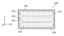
- FIG. 16 is a diagram showing a configuration outline when the light emitting device 130 according to the first embodiment includes a plurality of rows of LEDs 150.
- the light emitting device 130 shown in FIG. 16 includes the LEDs 150 arranged in three rows.
- the second wavelength conversion material 162 is laterally and outwardly of at least one of the LEDs 150 among the LEDs 150.
- the sealing member 160 when arranging a plurality of LEDs 150 on the base 140, it is not necessary to form the sealing member 160 for each row, for example, the sealing member 160 separated for each LED 150 May be formed.
- the groove 145 is provided in a recessed shape in the base 140 parallel to the thickness direction (Z-axis direction) of the plate-shaped base 140.
- the grooves 145 may be recessed in the base 140 in a direction oblique to the thickness direction of the base 140.
- the groove 145 having a depth direction in an oblique direction to the thickness direction of the substrate 140 can be formed.
- the groove 145 is inclined so that the bottom surface of the groove 145 approaches the left side surface of the base 140.
- an optical path length of light traveling from the LED 150 in the direction of the groove 145 (for example, a dotted arrow in FIG. 5) passing through the second wavelength conversion material 162 accommodated in the groove 145 is as shown in FIG.
- the depth direction is longer than when parallel to the Z-axis direction.
- the groove 145 when the groove 145 is recessed in the direction oblique to the thickness direction of the base 140 in this manner, for example, the optical path length necessary for conversion to the predetermined wavelength by the second wavelength conversion material 162 is maintained In addition, the width of the groove 145 can be narrowed. As a result, the total amount of the phosphor-containing resin including the second wavelength conversion material 162 contained in the groove 145 can be reduced.
- the groove 145 in the first embodiment has a rectangular cross section perpendicular to the longitudinal direction (the X axis direction in FIG. 3).
- the cross-sectional shape of the groove 145 does not have to be a quadrangle, and may be configured entirely or partially by a curve.
- the cross-sectional shape of the groove 145 may be a polygon other than a quadrangle such as a triangle.
- the cross-sectional shape is not limited, and the cross-sectional shape does not have to be the same over the entire length of the groove 145.
- grooves 145 do not have to be provided on the base 140 at positions on both sides of the LED 150.
- the groove 145 should be provided only on the near side. Good.
- FIG. 17 is a perspective view of a light bulb shaped lamp 100 according to Embodiment 2 of the present invention.
- FIG. 18 is an exploded perspective view of a light bulb shaped lamp 100 according to a second embodiment of the present invention.
- FIG. 19 is a front view of a light bulb shaped lamp 100 according to Embodiment 2 of the present invention.
- the lighting circuit 180 and a part of the lead wire 170 for feeding and holding, which are located inside the base 190, are indicated by dotted lines.
- the light bulb shaped lamp 100 is a light bulb in which a base 190 is attached to a translucent globe 110.
- a light emitting device 130 which is an LED module mounted with LEDs, is housed.
- the light emitting device 130 is fixed to a stem 120 which extends from the opening 111 of the globe 110 into the globe 110.
- the light bulb shaped lamp 100 includes a globe 110, a stem 120, a light emitting device 130, two lead wires 170, a lighting circuit 180 and a cap 190. Equipped with
- the globe 110 is a hollow member made of silica glass that is transparent to visible light. Therefore, the user can view the light emitting device 130 stored in the glove 110 from the outside of the glove 110.
- the bulb-shaped lamp 100 can suppress the loss of light generated by the LED 150 by the globe 110. Furthermore, the light bulb shaped lamp 100 can obtain high heat resistance.
- the shape of the glove 110 is a shape in which one end is closed spherically and the other end has an opening 111.
- the shape of the globe 110 is such that a part of the hollow sphere is narrowed while extending in a direction away from the center of the sphere, and the opening 111 is formed at a position away from the center of the sphere.
- the shape of the globe 110 is an A-shape (JIS C7710) similar to a general incandescent lamp.
- the shape of the glove 110 does not have to be A-shaped.
- the shape of the glove 110 may be G-shaped or E-shaped or the like.
- the glove 110 does not have to be made of silica glass.
- the glove 110 may be a member made of resin such as acrylic.
- the stem 120 is provided to extend from the opening 111 of the glove 110 into the glove 110. Specifically, at one end of the stem 120, a rod-like extending portion 120a extending in the Z direction to the vicinity of the light emitting device 130 is formed. That is, the stem 120 according to the present embodiment is a member in which a stem used for a general incandescent lamp is extended into the globe 110.
- a light emitting device 130 is fixed to the tip of the extending portion 120a.
- the other end of the stem 120 is flared to match the shape of the opening 111.
- the other end of the flared stem 120 is joined to the opening 111 of the glove 110 so as to close the opening of the glove 110.
- the stem 120 a part of each of the two lead wires 170 is sealed.
- the bulb-shaped lamp 100 can prevent water or water vapor and the like from intruding into the glove 110 for a long period of time, and the deterioration of the light emitting device 130 due to moisture and the connection portion between the light emitting device 130 and the lead wire Deterioration can be suppressed.
- the stem 120 is made of soft glass which is transparent to visible light.
- the light bulb shaped lamp 100 can suppress the loss of the light generated by the LED 150 by the stem 120.
- the bulb-shaped lamp 100 can also prevent the stem 120 from forming a shadow.
- the stem 120 emits light due to the light emitted from the LED 150, the light bulb shaped lamp 100 can also exhibit a visually excellent appearance.
- the stem 120 does not necessarily have to be transparent to visible light and does not have to be made of soft glass.
- the stem 120 may be a member made of a high thermal conductivity resin.
- a high thermal conductivity resin for example, a silicone resin mixed with metal particles such as alumina or zinc oxide may be used.
- the light bulb shaped lamp 100 can actively dissipate the heat generated by the light emitting device 130 to the glove 110 or the cap 190 via the stem 120. As a result, the light bulb shaped lamp 100 can suppress the decrease in the light emission efficiency and the decrease in the life of the LED 150 due to the temperature rise.
- the stem 120 does not necessarily have to close the opening of the glove 110, and may be attached to a part of the opening 111.
- the two lead wires 170 are connected to the light emitting device 130, and the power supplied from the base 190 is supplied to the plurality of LEDs 150 via the two lead wires 170.
- the lead wire 170 is preferably a metal wire containing copper having a high thermal conductivity.
- the heat generated by the light emitting device 130 can be positively dissipated to the base 190 via the lead wire 170.
- the number of lead wires 170 is not necessarily two.
- the light bulb shaped lamp 100 when the light bulb shaped lamp 100 is provided with a plurality of light emitting devices 130 in the globe 110, the light bulb shaped lamp 100 may be provided with two lead wires 170 for each light emitting device 130.
- the lead wire 170 is preferably attached to the base 140 so as to press the base 140 toward the stem 120. This makes it possible to fix and hold the base 140 to the stem 120 more firmly.
- the lighting circuit 180 is a circuit for causing the LED 150 to emit light, and is housed in the base 190.
- lighting circuit 180 includes a plurality of circuit elements and a circuit board on which each circuit element is mounted.
- the lighting circuit 180 converts AC power received from the base 190 into DC power, and supplies the DC power to the plurality of LEDs 150 via the two lead wires 170.
- the light emitting device 130 is the light emitting device 130 in the first embodiment of the present invention described above.
- the light emitting device 130 shown in FIGS. 1 to 5 is employed as a light source of the light bulb shaped lamp 100.
- white light is emitted in a wide range including the lower side of the light emitting device 130 and all sides.
- the light emitting device 130 having the wavelength conversion portion 165 on the back surface shown in FIG. 6 is adopted as a light source of the bulb-shaped lamp 100, all light distribution characteristics similar to the incandescent bulb using a filament as a light source Can.
- Each of the light emitting devices 130 shown in FIGS. 7 to 16 may also be employed as a light source of the light bulb shaped lamp 100.
- the light emitting device 130 is supported by the stem 120.
- the light emitting device 130 may not be supported by the stem 120.
- light emitting device 130 may be supported by only two leads 170.
- the light-bulb-shaped lamp 100 provided with the light-emitting device 130 was demonstrated in this Embodiment, the light-emitting device 130 may be employ
- the light emitting device 130 may be employed as a light source of a straight tube lamp.
- the light emitting device 130 provided with the wavelength conversion portion 165 on the back surface shown in FIG. 6 is adopted as a light source of a straight tube lamp, all light distribution characteristics similar to a general straight tube fluorescent lamp can be obtained.
- the light emitting device 130 may be adopted as a light source of an annular lamp.
- the light emitting device 130 by forming the entire shape of the light emitting device 130 shown in FIG. 1 to be curved according to the ring shape of the annular lamp, the light emitting device 130 can be installed on the annular lamp without difficulty. .
- the light emitting device 130 is not limited to a particular type of lamp, and can be used as a light source for various types of lamps.
- a blue LED chip is adopted as the LED 150, and yellow phosphor particles are adopted as a wavelength conversion material from blue light to white light.
- the combination of the LED 150 and the phosphor particles is not limited to this combination.
- the light emitting device 130 emits white light by a blue LED chip that emits blue light, and green phosphor particles that are excited by blue light to emit green light and red phosphor particles that emit red light. It is also good.
- the light emitting device 130 is an ultraviolet LED chip that emits ultraviolet light having a wavelength shorter than that of blue light, and blue phosphor particles that are mainly excited by the ultraviolet light to emit blue light, red light and green light.
- White light may be emitted by the green phosphor particles and the red phosphor particles.
- Embodiment 1 when arranging several LED150, as shown in FIG.1 and FIG.16 grade
- the wavelength conversion portion 165 which is a sintered body film is formed on the back surface of the base 140, the arrangement position of the wavelength conversion portion 165 is not the back surface. It is also good.
- the wavelength conversion unit 165 may be formed on an arrangement surface which is a surface on which the LEDs 150 are arranged. In this case, the LED 150 is mounted on the wavelength converter 165.
- the LED 150 is disposed only on one of the two main surfaces perpendicular to the thickness direction of the plate-like base 140 (arrangement surface in the first embodiment). However, the LEDs 150 may be placed on both the placement side and the back side.
- the light emitting device 130 provided with the wavelength conversion portion 165 or the reflective film 167 on the back surface of the base 140 has been described with reference to FIGS. 6 and 7.
- the back surface of the base 140 may be provided with other elements.
- a heat sink for dissipating heat may be disposed on the back surface of the base 140.
- the second wavelength conversion material 162 accommodated in the groove 145 is the same as the case where the reflective film 167 is disposed on the back surface of the base 140.
- the emission of white light to the side of 140 is realized.
- the light emitting device 130 having a heat sink may be employed as a light source for each of the light bulb shaped lamp 100, the straight tube type lamp, and the ring shaped lamp described in the second embodiment.
- the substrate 140 is a substrate made of glass or the like.
- the base 140 does not have to be a plate-like member, and may be, for example, a rod-like member or a member having a curved surface.
- an LED is illustrated as a semiconductor light emitting element included in the light emitting device 130 in the first and second embodiments.
- the semiconductor light emitting element provided in the light emitting device 130 may be a semiconductor laser or an organic EL (Electro Luminescence).
- the present invention can be widely used as a light emitting device including a semiconductor light emitting element, a lamp including the light emitting device, and the like.
- Reference Signs List 100 light bulb shaped lamp 110 globe 111 opening 120 stem 120 a extension 130 light emitting device 140 base 145 groove 150 LED 160 sealing member 161 first wavelength conversion material 162 second wavelength conversion material 165 wavelength conversion part 166 third wavelength conversion material 167 reflection film 170 lead wire 180 lighting circuit
Abstract
Priority Applications (4)
| Application Number | Priority Date | Filing Date | Title |
|---|---|---|---|
| EP11832061A EP2492979A4 (fr) | 2010-12-27 | 2011-08-23 | Dispositif émetteur de lumière et lampe |
| JP2011547095A JP4926303B1 (ja) | 2010-12-27 | 2011-08-23 | 発光装置およびランプ |
| US13/503,242 US8421111B2 (en) | 2010-12-27 | 2011-08-23 | Light-emitting device and lamp |
| CN2011900002261U CN202721174U (zh) | 2010-12-27 | 2011-08-23 | 发光装置及灯 |
Applications Claiming Priority (2)
| Application Number | Priority Date | Filing Date | Title |
|---|---|---|---|
| JP2010290928 | 2010-12-27 | ||
| JP2010-290928 | 2010-12-27 |
Publications (1)
| Publication Number | Publication Date |
|---|---|
| WO2012090350A1 true WO2012090350A1 (fr) | 2012-07-05 |
Family
ID=46382496
Family Applications (1)
| Application Number | Title | Priority Date | Filing Date |
|---|---|---|---|
| PCT/JP2011/004678 WO2012090350A1 (fr) | 2010-12-27 | 2011-08-23 | Dispositif émetteur de lumière et lampe |
Country Status (4)
| Country | Link |
|---|---|
| US (1) | US8421111B2 (fr) |
| EP (1) | EP2492979A4 (fr) |
| CN (1) | CN202721174U (fr) |
| WO (1) | WO2012090350A1 (fr) |
Cited By (9)
| Publication number | Priority date | Publication date | Assignee | Title |
|---|---|---|---|---|
| WO2014083781A1 (fr) * | 2012-11-30 | 2014-06-05 | パナソニック株式会社 | Appareil électroluminescent et source électroluminescente |
| WO2014181757A1 (fr) | 2013-05-09 | 2014-11-13 | 日東電工株式会社 | Carte de circuit imprimé, dispositif à semi-conducteur optique et procédé de fabrication associé |
| JP2015056666A (ja) * | 2013-09-11 | 2015-03-23 | 廣▲ジャー▼光電股▲ふん▼有限公司 | 発光モジュール及びそれに関する照明装置 |
| JP2015056667A (ja) * | 2013-09-11 | 2015-03-23 | 廣▲ジャー▼光電股▲ふん▼有限公司 | 可撓性発光ダイオードモジュール及び発光ダイオード電球 |
| JP2015076612A (ja) * | 2013-10-07 | 2015-04-20 | 廣▲ジャー▼光電股▲ふん▼有限公司 | 発光ダイオードモジュール及びその製造方法 |
| JP2016115947A (ja) * | 2014-07-30 | 2016-06-23 | 高玉宇 | 蛍光複合樹脂基板白色発光ダイオード |
| KR20170060335A (ko) * | 2015-11-24 | 2017-06-01 | 엘지이노텍 주식회사 | 발광 소자 패키지 및 이를 포함하는 차량용 조명 장치 |
| US9680075B2 (en) | 2012-08-31 | 2017-06-13 | Panasonic Intellectual Property Management Co., Ltd. | Light-emitting device |
| US20240011621A1 (en) * | 2020-11-27 | 2024-01-11 | Kyocera Corporation | Light emission device and illumination apparatus |
Families Citing this family (23)
| Publication number | Priority date | Publication date | Assignee | Title |
|---|---|---|---|---|
| EP2562147A4 (fr) | 2010-04-19 | 2013-09-18 | Panasonic Corp | Composition de verre, dispositif source lumineuse et dispositif d'éclairage |
| KR101641860B1 (ko) * | 2010-05-12 | 2016-07-29 | 엘지이노텍 주식회사 | 발광소자 어레이, 조명장치 및 백라이트 장치 |
| US8192051B2 (en) | 2010-11-01 | 2012-06-05 | Quarkstar Llc | Bidirectional LED light sheet |
| US8410726B2 (en) | 2011-02-22 | 2013-04-02 | Quarkstar Llc | Solid state lamp using modular light emitting elements |
| US8314566B2 (en) | 2011-02-22 | 2012-11-20 | Quarkstar Llc | Solid state lamp using light emitting strips |
| CN105826311B (zh) | 2011-04-20 | 2019-06-25 | 松下知识产权经营株式会社 | 发光装置、背光单元、液晶显示装置以及照明装置 |
| US8835945B2 (en) * | 2013-01-11 | 2014-09-16 | Lighting Science Group Corporation | Serially-connected light emitting diodes, methods of forming same, and luminaires containing same |
| US9360202B2 (en) | 2011-05-13 | 2016-06-07 | Lighting Science Group Corporation | System for actively cooling an LED filament and associated methods |
| KR20140066974A (ko) | 2011-09-26 | 2014-06-03 | 파나소닉 주식회사 | 발광 장치의 제조 방법 및 발광 장치 |
| US9423118B2 (en) * | 2011-11-15 | 2016-08-23 | Panasonic Intellectual Property Management Co., Ltd. | Light-emitting module and lamp using same |
| US20150023014A1 (en) * | 2012-02-16 | 2015-01-22 | Panasonic Corporation | Lamp and lighting apparatus |
| CN103591480B (zh) * | 2012-08-17 | 2016-02-17 | 展晶科技(深圳)有限公司 | 发光二极管照明装置 |
| CN103807622B (zh) * | 2012-11-09 | 2018-04-24 | 欧司朗有限公司 | 照明装置 |
| TWM461732U (zh) * | 2013-04-10 | 2013-09-11 | Wintek Corp | 光源模組 |
| CN103335226A (zh) * | 2013-06-19 | 2013-10-02 | 福建省万邦光电科技有限公司 | 一种全方向出光的led球泡灯 |
| CN104633486B (zh) * | 2013-11-07 | 2018-09-07 | 陈宗烈 | 一种led灯泡 |
| CN105322433B (zh) * | 2014-05-28 | 2020-02-04 | 深圳光峰科技股份有限公司 | 波长转换装置及其相关发光装置 |
| CN105322072B (zh) * | 2014-07-30 | 2019-08-06 | 盛汉有限公司 | 萤光复合树脂基板白光发光二级管装置及其制造方法 |
| DE102014015695B4 (de) * | 2014-10-21 | 2020-02-06 | Isophon Glas Gmbh | Glasplatte und Glasanordnung |
| DE102016117594A1 (de) * | 2016-09-19 | 2018-03-22 | Osram Opto Semiconductors Gmbh | Licht emittierende Vorrichtung |
| EP3480510B1 (fr) * | 2017-11-03 | 2020-03-25 | Xiamen Eco Lighting Co., Ltd. | Appareil d'éclairage à del |
| EP3514440B1 (fr) * | 2018-01-18 | 2021-12-29 | BGT Materials Limited | Procédé de fabrication d'une ampoule bulbe à dels comportant des filaments de rayonnement thermique |
| CN110081323B (zh) * | 2018-05-23 | 2021-08-31 | 浙江山蒲照明电器有限公司 | Led灯丝及led球泡灯 |
Citations (9)
| Publication number | Priority date | Publication date | Assignee | Title |
|---|---|---|---|---|
| JP2000315824A (ja) * | 1999-04-30 | 2000-11-14 | Runaraito Kk | 発光ダイオードおよびその製造方法 |
| US20020021085A1 (en) * | 2000-08-09 | 2002-02-21 | Ng Kee Yean | Light emitting devices |
| JP2006313717A (ja) | 2005-04-08 | 2006-11-16 | Toshiba Lighting & Technology Corp | 電球型ランプ |
| JP2007123885A (ja) * | 2005-10-28 | 2007-05-17 | Iled Photoelectronics Inc | 白光ledパッケージ構造 |
| JP2008066691A (ja) * | 2006-03-10 | 2008-03-21 | Toshiba Lighting & Technology Corp | 照明装置 |
| JP2009043447A (ja) | 2007-08-06 | 2009-02-26 | Sharp Corp | 照明装置 |
| JP2010141119A (ja) * | 2008-12-11 | 2010-06-24 | Nitto Denko Corp | 光半導体封止用シート |
| JP2010229002A (ja) * | 2009-03-30 | 2010-10-14 | Nippon Electric Glass Co Ltd | 蛍光体複合材料に用いられるSnO−P2O5系ガラス |
| JP2010283281A (ja) * | 2009-06-08 | 2010-12-16 | Nichia Corp | 発光装置 |
Family Cites Families (9)
| Publication number | Priority date | Publication date | Assignee | Title |
|---|---|---|---|---|
| JP2003110146A (ja) | 2001-07-26 | 2003-04-11 | Matsushita Electric Works Ltd | 発光装置 |
| TW552726B (en) | 2001-07-26 | 2003-09-11 | Matsushita Electric Works Ltd | Light emitting device in use of LED |
| JP4046118B2 (ja) | 2002-05-28 | 2008-02-13 | 松下電工株式会社 | 発光素子、それを用いた発光装置及び面発光照明装置 |
| US7758223B2 (en) | 2005-04-08 | 2010-07-20 | Toshiba Lighting & Technology Corporation | Lamp having outer shell to radiate heat of light source |
| JP2007165811A (ja) * | 2005-12-16 | 2007-06-28 | Nichia Chem Ind Ltd | 発光装置 |
| US8337048B2 (en) | 2007-10-31 | 2012-12-25 | Yu-Nung Shen | Light source package having a six sided light emitting die supported by electrodes |
| JP5276412B2 (ja) * | 2008-11-04 | 2013-08-28 | キヤノン株式会社 | 機能性領域の移設方法、ledアレイ、ledプリンタヘッド、及びledプリンタ |
| CN202839730U (zh) * | 2010-12-28 | 2013-03-27 | 松下电器产业株式会社 | 发光装置、发光模块及灯 |
| CN103080631A (zh) | 2011-01-14 | 2013-05-01 | 松下电器产业株式会社 | 灯及照明装置 |
-
2011
- 2011-08-23 CN CN2011900002261U patent/CN202721174U/zh not_active Expired - Fee Related
- 2011-08-23 EP EP11832061A patent/EP2492979A4/fr not_active Withdrawn
- 2011-08-23 US US13/503,242 patent/US8421111B2/en not_active Expired - Fee Related
- 2011-08-23 WO PCT/JP2011/004678 patent/WO2012090350A1/fr active Application Filing
Patent Citations (9)
| Publication number | Priority date | Publication date | Assignee | Title |
|---|---|---|---|---|
| JP2000315824A (ja) * | 1999-04-30 | 2000-11-14 | Runaraito Kk | 発光ダイオードおよびその製造方法 |
| US20020021085A1 (en) * | 2000-08-09 | 2002-02-21 | Ng Kee Yean | Light emitting devices |
| JP2006313717A (ja) | 2005-04-08 | 2006-11-16 | Toshiba Lighting & Technology Corp | 電球型ランプ |
| JP2007123885A (ja) * | 2005-10-28 | 2007-05-17 | Iled Photoelectronics Inc | 白光ledパッケージ構造 |
| JP2008066691A (ja) * | 2006-03-10 | 2008-03-21 | Toshiba Lighting & Technology Corp | 照明装置 |
| JP2009043447A (ja) | 2007-08-06 | 2009-02-26 | Sharp Corp | 照明装置 |
| JP2010141119A (ja) * | 2008-12-11 | 2010-06-24 | Nitto Denko Corp | 光半導体封止用シート |
| JP2010229002A (ja) * | 2009-03-30 | 2010-10-14 | Nippon Electric Glass Co Ltd | 蛍光体複合材料に用いられるSnO−P2O5系ガラス |
| JP2010283281A (ja) * | 2009-06-08 | 2010-12-16 | Nichia Corp | 発光装置 |
Non-Patent Citations (1)
| Title |
|---|
| See also references of EP2492979A4 |
Cited By (16)
| Publication number | Priority date | Publication date | Assignee | Title |
|---|---|---|---|---|
| US9680075B2 (en) | 2012-08-31 | 2017-06-13 | Panasonic Intellectual Property Management Co., Ltd. | Light-emitting device |
| WO2014083781A1 (fr) * | 2012-11-30 | 2014-06-05 | パナソニック株式会社 | Appareil électroluminescent et source électroluminescente |
| JP5838309B2 (ja) * | 2012-11-30 | 2016-01-06 | パナソニックIpマネジメント株式会社 | 発光装置、照明用光源、および照明装置 |
| WO2014181757A1 (fr) | 2013-05-09 | 2014-11-13 | 日東電工株式会社 | Carte de circuit imprimé, dispositif à semi-conducteur optique et procédé de fabrication associé |
| JP2015056666A (ja) * | 2013-09-11 | 2015-03-23 | 廣▲ジャー▼光電股▲ふん▼有限公司 | 発光モジュール及びそれに関する照明装置 |
| JP2015056667A (ja) * | 2013-09-11 | 2015-03-23 | 廣▲ジャー▼光電股▲ふん▼有限公司 | 可撓性発光ダイオードモジュール及び発光ダイオード電球 |
| USRE49031E1 (en) | 2013-09-11 | 2022-04-12 | Epistar Corporation | Flexible LED assemblies and LED light bulbs |
| JP2015076612A (ja) * | 2013-10-07 | 2015-04-20 | 廣▲ジャー▼光電股▲ふん▼有限公司 | 発光ダイオードモジュール及びその製造方法 |
| US10319886B2 (en) | 2013-10-07 | 2019-06-11 | Epistar Corporation | LED assembly for omnidirectional light appliances |
| US10910528B2 (en) | 2013-10-07 | 2021-02-02 | Epistar Corporation | LED assembly |
| US11450791B2 (en) | 2013-10-07 | 2022-09-20 | Epistar Corporation | LED assembly for omnidirectional light applications |
| US11949050B2 (en) | 2013-10-07 | 2024-04-02 | Epistar Corporation | LED assembly |
| JP2016115947A (ja) * | 2014-07-30 | 2016-06-23 | 高玉宇 | 蛍光複合樹脂基板白色発光ダイオード |
| KR20170060335A (ko) * | 2015-11-24 | 2017-06-01 | 엘지이노텍 주식회사 | 발광 소자 패키지 및 이를 포함하는 차량용 조명 장치 |
| KR102413302B1 (ko) | 2015-11-24 | 2022-06-27 | 쑤저우 레킨 세미컨덕터 컴퍼니 리미티드 | 발광 소자 패키지 및 이를 포함하는 차량용 조명 장치 |
| US20240011621A1 (en) * | 2020-11-27 | 2024-01-11 | Kyocera Corporation | Light emission device and illumination apparatus |
Also Published As
| Publication number | Publication date |
|---|---|
| EP2492979A4 (fr) | 2012-11-28 |
| CN202721174U (zh) | 2013-02-06 |
| EP2492979A1 (fr) | 2012-08-29 |
| US20120235181A1 (en) | 2012-09-20 |
| US8421111B2 (en) | 2013-04-16 |
Similar Documents
| Publication | Publication Date | Title |
|---|---|---|
| WO2012090350A1 (fr) | Dispositif émetteur de lumière et lampe | |
| JP5147997B2 (ja) | 発光装置、電球形ランプ及び照明装置 | |
| JP5276226B2 (ja) | 実装用基板、発光装置及びランプ | |
| EP2492978B1 (fr) | Dispositif électroluminescent, module électroluminescent et lampe | |
| WO2012011279A1 (fr) | Lampe en forme d'ampoule | |
| JP6358457B2 (ja) | 発光装置、照明用光源及び照明装置 | |
| JP6233750B2 (ja) | 発光装置およびその製造方法、照明用光源、並びに照明装置 | |
| JP2016167518A (ja) | 発光装置、及び、照明装置 | |
| JP6268636B2 (ja) | 発光装置、照明用光源及び照明装置 | |
| JP4926303B1 (ja) | 発光装置およびランプ | |
| JP5838309B2 (ja) | 発光装置、照明用光源、および照明装置 | |
| JP5351365B1 (ja) | 発光装置及びランプ | |
| WO2014013671A1 (fr) | Lampe de type à ampoule et dispositif d'éclairage | |
| JP2018121032A (ja) | 発光装置及び照明装置 | |
| JP4928013B1 (ja) | 発光装置、発光モジュール及びランプ | |
| WO2015072120A1 (fr) | Dispositif émettant de la lumière, module émettant de la lumière, dispositif d'éclairage et lampe | |
| JP2016058650A (ja) | 発光装置、照明用光源、及び照明装置 | |
| JP5563730B1 (ja) | 照明用光源及び照明装置 | |
| JP5420118B1 (ja) | 電球形ランプ及び照明装置 | |
| JP5793721B2 (ja) | 照明用光源及び照明装置 | |
| JP2013201380A (ja) | 反射材及び照明装置 | |
| JP2018041806A (ja) | 発光装置、及び、照明装置 | |
| JP2015176968A (ja) | 発光装置およびその製造方法、照明用光源、並びに照明装置 |
Legal Events
| Date | Code | Title | Description |
|---|---|---|---|
| WWE | Wipo information: entry into national phase |
Ref document number: 201190000226.1 Country of ref document: CN |
|
| WWE | Wipo information: entry into national phase |
Ref document number: 2011547095 Country of ref document: JP |
|
| WWE | Wipo information: entry into national phase |
Ref document number: 13503242 Country of ref document: US Ref document number: 2011832061 Country of ref document: EP |
|
| WWE | Wipo information: entry into national phase |
Ref document number: 3962/CHENP/2012 Country of ref document: IN |
|
| 121 | Ep: the epo has been informed by wipo that ep was designated in this application |
Ref document number: 11832061 Country of ref document: EP Kind code of ref document: A1 |
|
| 121 | Ep: the epo has been informed by wipo that ep was designated in this application |
Ref document number: 11832061 Country of ref document: EP Kind code of ref document: A1 |
|
| NENP | Non-entry into the national phase |
Ref country code: DE |