WO2012086091A1 - フィルム基板の液晶注入方法、及び、フィルム基板の液晶注入装置 - Google Patents
フィルム基板の液晶注入方法、及び、フィルム基板の液晶注入装置 Download PDFInfo
- Publication number
- WO2012086091A1 WO2012086091A1 PCT/JP2010/073463 JP2010073463W WO2012086091A1 WO 2012086091 A1 WO2012086091 A1 WO 2012086091A1 JP 2010073463 W JP2010073463 W JP 2010073463W WO 2012086091 A1 WO2012086091 A1 WO 2012086091A1
- Authority
- WO
- WIPO (PCT)
- Prior art keywords
- liquid crystal
- film substrate
- crystal injection
- contact
- injection method
- Prior art date
- Legal status (The legal status is an assumption and is not a legal conclusion. Google has not performed a legal analysis and makes no representation as to the accuracy of the status listed.)
- Ceased
Links
Images











Classifications
-
- B—PERFORMING OPERATIONS; TRANSPORTING
- B32—LAYERED PRODUCTS
- B32B—LAYERED PRODUCTS, i.e. PRODUCTS BUILT-UP OF STRATA OF FLAT OR NON-FLAT, e.g. CELLULAR OR HONEYCOMB, FORM
- B32B37/00—Methods or apparatus for laminating, e.g. by curing or by ultrasonic bonding
- B32B37/14—Methods or apparatus for laminating, e.g. by curing or by ultrasonic bonding characterised by the properties of the layers
-
- G—PHYSICS
- G02—OPTICS
- G02F—OPTICAL DEVICES OR ARRANGEMENTS FOR THE CONTROL OF LIGHT BY MODIFICATION OF THE OPTICAL PROPERTIES OF THE MEDIA OF THE ELEMENTS INVOLVED THEREIN; NON-LINEAR OPTICS; FREQUENCY-CHANGING OF LIGHT; OPTICAL LOGIC ELEMENTS; OPTICAL ANALOGUE/DIGITAL CONVERTERS
- G02F1/00—Devices or arrangements for the control of the intensity, colour, phase, polarisation or direction of light arriving from an independent light source, e.g. switching, gating or modulating; Non-linear optics
- G02F1/01—Devices or arrangements for the control of the intensity, colour, phase, polarisation or direction of light arriving from an independent light source, e.g. switching, gating or modulating; Non-linear optics for the control of the intensity, phase, polarisation or colour
- G02F1/13—Devices or arrangements for the control of the intensity, colour, phase, polarisation or direction of light arriving from an independent light source, e.g. switching, gating or modulating; Non-linear optics for the control of the intensity, phase, polarisation or colour based on liquid crystals, e.g. single liquid crystal display cells
- G02F1/133—Constructional arrangements; Operation of liquid crystal cells; Circuit arrangements
- G02F1/1333—Constructional arrangements; Manufacturing methods
- G02F1/1341—Filling or closing of cells
-
- Y—GENERAL TAGGING OF NEW TECHNOLOGICAL DEVELOPMENTS; GENERAL TAGGING OF CROSS-SECTIONAL TECHNOLOGIES SPANNING OVER SEVERAL SECTIONS OF THE IPC; TECHNICAL SUBJECTS COVERED BY FORMER USPC CROSS-REFERENCE ART COLLECTIONS [XRACs] AND DIGESTS
- Y10—TECHNICAL SUBJECTS COVERED BY FORMER USPC
- Y10T—TECHNICAL SUBJECTS COVERED BY FORMER US CLASSIFICATION
- Y10T156/00—Adhesive bonding and miscellaneous chemical manufacture
- Y10T156/17—Surface bonding means and/or assemblymeans with work feeding or handling means
Definitions
- the embodiment described in the present specification relates to a liquid crystal injection method and a liquid crystal injection device for a film substrate, in which a liquid crystal material is injected into the film substrate.
- a transparent substrate to which a transparent electrode is added is bonded so that the electrode faces the other substrate, the liquid crystal material is sealed between the transparent substrates, and a voltage is applied between the electrodes to react the liquid crystal material.
- a liquid crystal panel that performs display is known.
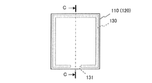
- the first substrate 110 and the second substrate 120 are bonded together by a rectangular sealing frame portion 130.
- an opening 131 for injecting a liquid crystal material is formed on one of the four sides.
- the sealing frame portion 130 seals a liquid crystal material described later between the first substrate 110 and the second substrate 120.
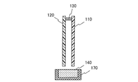
- the first substrate 110 and the second substrate 120 bonded together by the sealing frame portion 130 are housed in a housing (not shown), and the pressure inside the housing is reduced to, for example, a vacuum by the pressure reducing means. (Depressurized state).
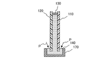
- the first substrate 110 and the second substrate 120 are shown in FIGS. 6A and 6B of the sealing frame portion 130 in the liquid crystal material 140 in the liquid crystal reservoir 170 while being in a reduced pressure state. Immerse the opening 131 side.
- the first substrate 110 and the second substrate 120 have the opening 131 (see FIGS. 6A and 6B) of the sealing frame portion 130 in the sealing material 151 in the sealing material reservoir 180. See) Immerse the side.
- the ultraviolet irradiation unit 160 cures the adhering sealing material 151 by the ultraviolet UV (cured sealing material 152). Then, as shown in FIG. 7I, a part 152 ′ of the cured sealing material 152 is removed along the surfaces of the first substrate 110 and the second substrate 120.
- the jig having a recess for accommodating the liquid crystal material corresponding to the injection amount is moved up to the outside of the liquid crystal material and brought into close contact with the liquid crystal injection port to inject the liquid crystal material.
- a method is known (see, for example, Patent Document 1).
- JP 2004-341236 A Japanese Patent Laid-Open No. 2005-181601 JP 2005-345500 A
- a plurality of liquid crystal panels 101 including a first substrate 110, a second substrate 120, and a sealing frame portion 130 are connected to the liquid crystal material 140 in the liquid crystal reservoir 170.
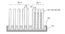
- the gap between the liquid crystal panels 101 is narrow (gap G1) as in the liquid crystal panel 101-1 shown on the right side of FIG. 8, the liquid crystal material 140 is placed between the liquid crystal panels 101 due to the surface tension as shown in FIG. Get in.
- the liquid crystal injection port 101a of the liquid crystal panel 101 is liquid crystal.
- the liquid crystal reservoir 170 is filled with a large amount of the liquid crystal material 140, and the liquid crystal injection port 101a is inserted therein.
- the liquid crystal injection port 101a hits the flat bottom of the liquid crystal reservoir 170, the liquid crystal injection port 101a is blocked, so that the liquid crystal panel 101 like the liquid crystal panel 101-3 on the left side of FIG. Is held by the jig so as to float at least the minimum gap (G3) from the bottom of the liquid crystal reservoir 170.
- the height of the liquid crystal injection port 101a may be shifted as in the central liquid crystal panel 101-4 or the right liquid crystal panel 101-5 in FIG. .
- the position of the liquid crystal injection port 101a where the liquid crystal injection port 101a is located at the uppermost position (away from the bottom of the liquid crystal reservoir 170) (the position of the right liquid crystal panel 101-5 in FIG. 9) is the lowest liquid level position S. Since the liquid crystal material 140 must be stored above the lowest liquid level position S, the liquid crystal material 140-1 above the lowest liquid level position S is filled in the liquid crystal panel 101. However, an extra liquid crystal material 140-2 below the lowest liquid level position S is necessary.
- the liquid crystal material 140 when the amount of the liquid crystal material 140 stored in the liquid crystal reservoir 170 increases, the liquid crystal material 140 is contaminated (such as absorption of moisture) because it takes a long time to contact the air, and the liquid crystal material 140 cannot be used and is wasted. There is a problem of generating materials.
- An object of the present invention is to provide a liquid crystal injection method and a liquid crystal injection device for a film substrate capable of reducing the amount of liquid crystal material stored in a liquid crystal reservoir.
- a liquid crystal injection method for a film substrate disclosed in the present specification is a liquid crystal injection method for a film substrate for injecting a liquid crystal material into the film substrate, and the film substrate is provided in a liquid crystal reservoir for storing the liquid crystal material.
- a liquid crystal injection device for a film substrate disclosed in the present specification is a liquid crystal injection device for a film substrate for injecting a liquid crystal material into the film substrate, and includes a liquid crystal reservoir for storing the liquid crystal material, and the liquid crystal reservoir is And a contact portion that forms a gap between the liquid crystal inlet of the film substrate and the bottom surface of the liquid crystal reservoir when the film substrate contacts.
- the amount of liquid crystal material stored in the liquid crystal reservoir can be reduced.
- FIG. 1B is a first cross-sectional view taken along the line AA in FIG. 1B.
- FIG. 2B is a cross-sectional view taken along the line AA in FIG.
- FIG. 1B is a first cross-sectional view taken along the line AA in FIG. 1B.
- FIG. 2B is a cross-sectional view taken along the line AA in FIG.
- FIG. 1B is a first cross-sectional view taken along the line AA in FIG.
- FIG. 2B is a cross-sectional view taken along the line AA in FIG.
- FIG. 6B It is an exploded view of a film substrate for explaining a conventional liquid crystal injection method. It is a top view of the film substrate for demonstrating the conventional liquid crystal injection
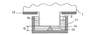
- FIGS. 1A and 1B are partial cross-sectional views illustrating a liquid crystal injection device 10 according to an embodiment.
- FIGS. 1A and 1B are cross-sectional views taken along the line AA in FIG. 1B.
- a liquid crystal injection device 10 shown in FIGS. 1A and 1B includes a liquid crystal reservoir 11 in which a liquid crystal material 2 is stored, and a jig 12 that supports the film substrate 1 at least vertically upward.
- the film substrate 1 is a liquid crystal panel, for example.
- a liquid crystal material 2 is injected into the liquid crystal.
- the film substrate 1 is formed by bonding two substrates each made of a flexible film. At least one of these two substrates is transparent, and is bonded so that transparent electrodes (not shown) face each other.
- the film substrate 1 has a rectangular shape, and a protruding portion 1b protruding in a rectangular shape is formed on one of the four sides of the rectangle.
- the tip of the protrusion 1b is a liquid crystal injection port 1a into which the liquid crystal material 2 is injected.
- the liquid crystal reservoir 11 has a convex portion 13 which is an example of a contact portion.
- the convex portion 13 comes into contact with the film substrate 1 to form a gap G shown in FIG. 2A between the liquid crystal inlet 1 a of the film substrate 1 and the bottom surface of the liquid crystal reservoir 11.
- the convex portion 13 of the present embodiment protrudes upward from the bottom surface of the liquid crystal reservoir 11 and has a longitudinal direction in the arrangement direction of the film substrate 1. Specifically, the convex portion 13 is formed in a shape such that one of the three rectangular surfaces comes into contact with the bottom surface of the liquid crystal reservoir portion 11 by placing a triangular prism member in the arrangement direction of the film substrate 1. Presents a shape.
- the convex portion 13 is in line contact with a part of the liquid crystal injection port 11a of the film substrate 1 at the upper end extending linearly in the longitudinal direction.
- the protrusion 13 may be provided integrally with the liquid crystal reservoir 11 or may be provided by disposing another member in the liquid crystal reservoir 11.
- the jig 12 is disposed for each film substrate 1, and the plurality of jigs 12 are moved up and down independently of each other. Further, the jig 12 supports the film substrate 1 vertically upward on both sides of the bottom surface with the protruding portion 1b of the film substrate 1 interposed therebetween.
- the jig 12 supports, for example, the film substrate 1 in the horizontal direction so as to sandwich the protruding portion 1b of the film substrate 1 from both sides, or supports the film substrate 1 in the thickness direction horizontally on both sides of the protruding portion 1b. May prevent the film substrate 1 from tilting.
- a plurality of film substrates 1 are respectively supported by a plurality of jigs 12 that move up and down independently above a liquid crystal reservoir 11 that stores a liquid crystal material 2.
- the height of the liquid crystal inlet 1 a is shifted for each film substrate 1.
- the jig 12 descends so that the liquid crystal injection port 1 a of the film substrate 1 comes into contact with the convex portion 13 provided in the liquid crystal reservoir 11.
- gaps G are formed at equal intervals between the liquid crystal inlet 1a and the bottom surface of the liquid crystal reservoir 11 (contact process).
- the jig 12 descends, so that the support of the jig 12 with respect to the film substrate 1 is released vertically, and the liquid crystal injection ports of the plurality of film substrates 1 are released.
- the position of 1a coincides with the convex portion 13.
- the film substrate 1 can be positioned even if the support in the vertically upward direction is released.
- the liquid crystal material 2 is injected from the gap G into the liquid crystal injection port 1a with the film substrate 1 in contact with the convex portion 13 (injection step).
- the film substrate 1 is housed in a housing (not shown), the inside of the housing is in a decompressed state, and the liquid crystal injection port 1a is inserted into the liquid crystal material 2 in the contact process while being in the decompressed state.
- the liquid crystal material 2 is injected from the liquid crystal injection port 1a when the reduced pressure state becomes the normal pressure state.
- the liquid crystal material 2 gathers around the convex portion 13 due to surface tension.
- the collected liquid crystal becomes a liquid reservoir 2-1 and is injected into the film substrate 1 by contacting the liquid crystal injection port 1a.
- the liquid crystal reservoir 11 of the present embodiment is made of, for example, aluminum, and a fluorine coating portion (an example of a coating portion) that prevents the liquid crystal material 2 from entering the surface thereof is formed on the convex portion 13.
- the liquid crystal reservoir 2-1 is easily formed.
- the sealing material for sealing the liquid crystal material 2 is injected into the liquid crystal injection port 1a and cured by ultraviolet rays or the like, whereby the sealing of the liquid crystal material 2 on the film substrate 1 is completed. .
- the film substrate 1 comes into contact with the convex portion (contact portion) 13 provided in the liquid crystal reservoir 11 that stores the liquid crystal material 2, so that the liquid crystal inlet 1 a of the film substrate 1 A gap G is formed between the liquid crystal reservoir 11 and the bottom surface (contact process). Further, the liquid crystal material 2 is injected from the gap G into the liquid crystal injection port 1a in a state where the film substrate 1 is in contact with the convex portion 13 (injection step).
- the liquid crystal inlet 1 a of the film substrate 1 is blocked by the bottom surface of the liquid crystal reservoir 11. Further, by forming the convex portion 13 by setting the gap G necessary for injecting the liquid crystal material 2 to a minimum, for example, the liquid crystal material 2 is added to the liquid crystal reservoir portion 11 in accordance with the height variation of the film substrate 1. Can be avoided.
- the amount of the liquid crystal material 2 stored in the liquid crystal reservoir 11 can be reduced.
- the liquid crystal reservoir 11 is provided with a convex portion 13 which is an example of a contact portion with which the film substrate 1 comes into contact. Therefore, the amount of the liquid crystal material 2 stored in the liquid crystal reservoir 11 can be reduced with a simple configuration.
- the convex portion 13 is in line contact with the liquid crystal inlet 1 a of the film substrate 1. Therefore, the gap G between the liquid crystal injection port 1a and the bottom surface of the liquid crystal reservoir 11 can be made constant irrespective of the manufacturing accuracy of the film substrate 1, and the amount of the liquid crystal material 2 stored in the liquid crystal reservoir 11 Can be further reduced.
- the liquid reservoir of the liquid crystal material 2 formed on the convex portion 13 due to surface tension. 2-1 is injected into the liquid crystal injection port 1a. Therefore, the liquid crystal material 2 can be injected even if the liquid level of the liquid crystal material 2 is lower than the gap G between the liquid crystal injection port 1 a and the bottom surface of the liquid crystal reservoir 11, so that the liquid crystal material 2 is stored in the liquid crystal reservoir 11. The amount of the liquid crystal material 2 can be further reduced.
- substrate 1 is made to contact the convex part 13, and the film board
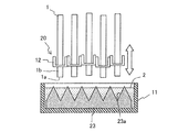
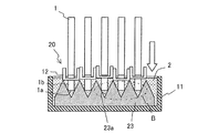
- FIG. 3A and 3B are partial cross-sectional views showing a liquid crystal injection device 20 according to another embodiment.
- FIG. 4 is an enlarged view of a portion B in FIG. 3B.
- the convex portion 13 is not provided, but the concave portion 23a of the protruding portion 23 is provided.
- the convex portion 13 is not provided, but the concave portion 23a of the protruding portion 23 is provided.
- a liquid crystal injection device 20 shown in FIGS. 3A and 3B includes a liquid crystal reservoir 11 in which the liquid crystal material 2 is stored, and a jig 12 that supports the film substrate 1 at least vertically upward.
- the film substrate 1 is a liquid crystal panel, for example.
- a liquid crystal material 2 is injected into the liquid crystal.
- the liquid crystal reservoir 11 has a recess 23a, which is an example of a contact portion, formed on the protrusion 23a.
- the recess 23 a comes into contact with the film substrate 1 to form a gap G shown in FIG. 4 between the liquid crystal inlet 1 a of the film substrate 1 and the bottom surface of the liquid crystal reservoir 11.
- the protrusion 23 protrudes upward from the bottom surface of the liquid crystal reservoir 11.
- the recess 23a is a groove having a longitudinal direction extending in a direction orthogonal to the arrangement direction of the film substrates 1 (longitudinal direction of the liquid crystal injection port 1a).
- the recess 23 a has a V-shaped cross section that is in line contact with the peripheral edge (two sides facing each other) of the injection port forming surface on which the liquid crystal injection port 1 a of the film substrate 1 is formed. It is a groove.
- the protrusion 23 may be provided integrally with the liquid crystal reservoir 11 or may be provided by arranging another member in the liquid crystal reservoir 11.
- a plurality of film substrates 1 are respectively supported by a plurality of jigs 12 that move up and down independently above a liquid crystal reservoir 11 that stores liquid crystal material 2.
- the height of the liquid crystal inlet 1 a is shifted for each film substrate 1.
- the liquid crystal injection port 1 a of the film substrate 1 is lined in two surfaces forming the V shape of the recess 23 a of the protrusion 23 provided in the liquid crystal reservoir 11. Contact. As a result, a gap G is formed between the liquid crystal inlet 1a and the bottom surface of the liquid crystal reservoir 11 (the bottom of the recess 23a in this embodiment) (contact process).
- the jig 12 descends, so that the support of the jig 12 to the film substrate 1 in the vertical direction is released, and the liquid crystal injection ports 1a of the plurality of film substrates 1 are released. Is coincident with the contact position with the recess 23a.
- the film substrate 1 can be positioned even if the support in the vertically upward direction is released.
- the liquid crystal material 2 is injected from the gap G into the liquid crystal injection port 1a (injection step).
- the sealing material for sealing the liquid crystal material 2 is injected into the liquid crystal injection port 1a and cured by ultraviolet rays or the like, whereby the sealing of the liquid crystal material 2 on the film substrate 1 is completed.
- the film substrate 1 comes into contact with the recess (contact portion) 23a provided in the liquid crystal reservoir 11 for storing the liquid crystal material 2, so that the liquid crystal injection port 1a of the film substrate 1 and A gap G is formed between the liquid crystal reservoir 11 and the bottom surface (contact process). Further, the liquid crystal material 2 is injected from the gap G into the liquid crystal injection port 1a in a state where the film substrate 1 is in contact with the recess 23a (injection step).
- the amount of the liquid crystal material 2 stored in the liquid crystal reservoir 11 can be reduced as in the above-described embodiment.
- the liquid crystal reservoir 11 is provided with a recess 23a of the protrusion 23 as an example of a contact portion with which the film substrate 1 comes into contact. Therefore, the amount of the liquid crystal material 2 can be reduced by collecting the liquid crystal material 2 in the recess 23a with a simple configuration. Furthermore, since the different liquid crystal material 2 can be stored for every recessed part 23a, the liquid crystal material 2 can also be simultaneously injected into a different kind of film board
- the recess 23a is in contact with the periphery (two sides facing each other) of the injection port forming surface on which the liquid crystal injection port 1a of the film substrate 1 is formed. Therefore, the gap G between the liquid crystal injection port 1a and the bottom surface of the liquid crystal reservoir 11 (the bottom of the recess 23a) can be made constant regardless of the manufacturing accuracy of the jig 12 and the film substrate 1, so that it is as narrow as possible. Liquid crystal can be injected at intervals, and the amount of the liquid crystal material 2 stored in the liquid crystal reservoir 11 can be further reduced.
- the concave portion 23a is a groove extending in the longitudinal direction of the liquid crystal injection port 1a. Therefore, the concave portion 23a contacts the liquid crystal injection port 1a over the longitudinal direction of the liquid crystal injection port 1a, so that the gap G between the liquid crystal injection port 1a and the bottom surface of the liquid crystal reservoir 11 (the bottom of the concave portion 23a) is surely secured. The amount of the liquid crystal material 2 stored in the liquid crystal reservoir 11 can be further reduced.
- the recess 23a is a groove having a V-shaped cross section. Therefore, the gap G between the liquid crystal inlet 1a and the bottom surface of the liquid crystal reservoir 11 (the bottom of the recess 23a) can be made constant by contacting the film substrate 1 on the two V-shaped surfaces. The amount of the liquid crystal material 2 stored in the reservoir 11 can be further reduced.
- the jig 12 that supports the film substrate 1 at least vertically upward is lowered to bring the film substrate 1 into contact with the recess 23a, and the jig after the film substrate 1 contacts the recess 23a.
- the support of the jig 12 vertically upward with respect to the film substrate 1 is released. Therefore, the variation in the height of the film substrate 1 can be reliably suppressed, and the amount of the liquid crystal material 2 stored in the liquid crystal reservoir 11 can be further reduced.
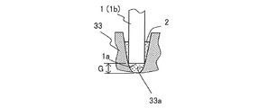
- the concave portion 23 a that is a groove having a V-shaped cross section formed in the protruding portion 23 has been described as an example of the contact portion, but the contact portion is described in FIG. 5.
- the liquid crystal stored in the liquid crystal reservoir 11 is the same as in the present embodiment, even in the case of the concave portion 33a which is a groove having a U-shaped cross section formed in the protruding portion 33 and other concave portions. The amount of the material 2 can be reduced.
- the convex portion 13 and the concave portions 23a and 33a have been described as examples of the contact portion.
- the contact portion is, for example, an uneven surface such as a rough surface.
Landscapes
- Physics & Mathematics (AREA)
- Nonlinear Science (AREA)
- Mathematical Physics (AREA)
- Chemical & Material Sciences (AREA)
- Crystallography & Structural Chemistry (AREA)
- General Physics & Mathematics (AREA)
- Optics & Photonics (AREA)
- Liquid Crystal (AREA)
Abstract
フィルム基板1に液晶材料2を注入するフィルム基板1の液晶注入方法であって、フィルム基板1を、液晶材料2を貯留する液晶溜め部11に設けられた接触部(13)に接触させることにより、フィルム基板1の液晶注入口1aと液晶溜め部11の底面との間に間隙Gを形成する接触工程と、フィルム基板1が接触部(13)に接触した状態で、上記間隙Gから液晶注入口1aに液晶材料2を注入する注入工程と、を含む。
Description
本明細書に記述された実施態様は、フィルム基板に液晶材料を注入する、フィルム基板の液晶注入方法及び液晶注入装置に関する。
従来、透明電極を付加した透明基板を他方の基板と電極が向き合うように貼り合わせ、透明基板の間に液晶材料を封止し、電極間に電圧を印加することにより、液晶材料を反応させて表示を行う液晶パネルが知られている。
液晶パネルに液晶材料を注入する方法として、第1の基板と第2の基板とを貼り合せるための封止枠部に設けた開口部から液晶材料を注入する方法がある。
この注入方法について、図6A~図6C及び図7A~図7Iを参照しながら簡単に説明する。
この注入方法について、図6A~図6C及び図7A~図7Iを参照しながら簡単に説明する。
図6A~図6Cに示すように、いずれも透明なフィルムからなる第1の基板110と第2の基板120とは、矩形の封止枠部130により貼り合わされる。この封止枠部130には、4辺のうちの1辺に、液晶材料注入用の開口部131が形成されている。封止枠部130は、後述する液晶材料を第1の基板110と第2の基板120との間で封止する。
図7Aに示すように封止枠部130により貼り合わされた第1の基板110及び第2の基板120は、図示しない筐体に収容され、減圧手段によって筐体内部が例えば真空になるまで減圧される(減圧状態)。
そして、図7Bに示すように、第1の基板110及び第2の基板120は、減圧状態のまま、液晶溜め部170内の液晶材料140に封止枠部130の図6A及び図6Bに示す開口部131側を浸漬する。
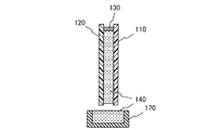
そして、図7C及び図7Dに示すように、図示しない筐体内の減圧状態が解除されて常圧状態になると、液晶材料140に外気圧Pが加わり、液晶材料140が封止枠部130内に充填される。その後、図7Eに示すように、第1の基板110及び第2の基板120が液晶溜め部170内の液晶材料140から取り出される。
そして、図7Fに示すように、第1の基板110及び第2の基板120は、封止材溜め部180内の封止材151に封止枠部130の開口部131(図6A及び図6B参照)側を浸漬する。
その後、図7Gに示すように、第1の基板110及び第2の基板120が封止材溜め部180内の封止材151から取り出されると、第1の基板110及び第2の基板120には、封止材151が付着する。
次に、図7Hに示すように、紫外線照射部160が紫外線UVによって、付着した封止材151を硬化させる(硬化封止材152)。そして、図7Iに示すように、第1の基板110及び第2の基板120の表面に沿って硬化封止材152の一部152´が除去される。
なお、液晶材料を注入する際に、注入量に相当する液晶材料を収容する凹みを有する冶具を、液晶材料の外まで上方に移動させて液晶注入口に密着させることで、液晶材料を注入する方法が知られている(例えば、特許文献1参照)。
また、液晶材料を注入する際に、液晶材料に浸される液晶吸引保持体を支持部材により支持した状態で、液晶吸引保持体から液晶注入口に液晶材料を注入する方法が知られている(例えば、特許文献2参照)。
また、液晶材料を注入する際に、液晶材料に浸される液晶吸引保持体を位置決め部材により位置決めした状態で、液晶吸引保持体から液晶注入口に液晶材料を注入する方法が知られている(例えば、特許文献3参照)。
ところで、図6A~図6C及び図7A~図7Iを参照しながら説明したように液晶材料を注入する方法では、開口部131からの液晶材料注入時に液晶材料140が不足すると、封止枠130内側に空気またはガスが侵入し液晶材料140が未充填となるため、封止枠部130に注入する量以上の液晶材料140が液晶溜め部170内に必要となる。
また、図8に示すように、第1の基板110と第2の基板120と封枠部130とを備える複数の液晶パネル101(液晶材料140注入前)を液晶溜め部170内の液晶材料140に挿入する場合、図8の右側に示す液晶パネル101-1のように液晶パネル101の間隔が狭いと(間隔G1)、図8に示すように表面張力によって液晶材料140が液晶パネル101の間に入り込んでしまう。
それに対し、図8の左側に示す液晶パネル101-2のように液晶パネル101の間隔を広くとると(ギャップG2)、液晶溜め部170に貯留される液晶材料140の量をそのギャップ分が増える事になる。
上述のように液晶パネル101の間隔をとるためには液晶材料140の量が余分に必要となるが、図9に示すように、液晶材料140の注入時に液晶パネル101の液晶注入口101aを液晶材料140内に維持するために、液晶溜め部170に多めの液晶材料140を満たし、その中に液晶注入口101aを挿入する方法がとられている。
具体的には、液晶溜め部170の平坦な底に液晶注入口101aが突き当たると液晶注入口101aが塞がれてしまうため、図9の左側の液晶パネル101-3のように、液晶パネル101は、液晶溜め部170の底との間に少なくとも最小ギャップ(G3)だけ浮かした状態に冶具により保持される。
しかし、液晶パネル101の製造精度や冶具の位置精度によっては、図9の中央の液晶パネル101-4や右側の液晶パネル101-5のように液晶注入口101aの高さにズレが生じてしまう。
そのため、液晶注入口101aが最も上方(液晶溜め部170の底から離れた)に位置する液晶注入口101aの位置(図9の右側の液晶パネル101-5の位置)が最低液面位置Sに設定されることになり、液晶材料140は、最低液面位置Sよりも上方まで貯留しなければならないため、最低液面位置Sよりも上方の液晶材料140-1は液晶パネル101内に充填されるが、最低液面位置Sよりも下方の液晶材料140-2は余分に必要ということになる。
一般に、液晶溜め部170に貯留される液晶材料140の量が増えると、液晶材料140が空気に触れる時間が長くなるため汚染(水分の吸収等)され、液晶材料140を使用できなくなり無駄な液晶材料を発生させるという問題がある。
本発明の目的は、液晶溜め部に貯留される液晶材料の量を低減することができるフィルム基板の液晶注入方法及び液晶注入装置を提供することである。
本明細書で開示するフィルム基板の液晶注入方法は、フィルム基板に液晶材料を注入するフィルム基板の液晶注入方法であって、前記フィルム基板を、前記液晶材料を貯留する液晶溜め部に設けられた接触部に接触させることにより、前記フィルム基板の液晶注入口と前記液晶溜め部の底面との間に間隙を形成する接触工程と、前記フィルム基板が前記接触部に接触した状態で、前記間隙から前記液晶注入口に前記液晶材料を注入する注入工程と、を含む。
本明細書で開示するフィルム基板の液晶注入装置は、フィルム基板に液晶材料を注入するフィルム基板の液晶注入装置であって、前記液晶材料が貯留される液晶溜め部を備え、前記液晶溜め部は、前記フィルム基板が接触することにより該フィルム基板の液晶注入口と前記液晶溜め部の底面との間に間隙を形成する接触部を有する。
本明細書で開示するフィルム基板の液晶注入方法及び液晶注入装置によれば、液晶溜め部に貯留される液晶材料の量を低減することができる。
以下、実施の形態に係るフィルム基板の液晶注入方法について、図面を参照しながら説明する。
図1A及び図1Bは、一実施の形態に係る液晶注入装置10を示す部分断面図である。
図1A及び図1Bは、一実施の形態に係る液晶注入装置10を示す部分断面図である。
図2A及び図2Bは、図1BのA-A断面図である。
図1A及び図1Bに示す液晶注入装置10は、液晶材料2が貯留される液晶溜め部11と、フィルム基板1を少なくとも鉛直上方に支持する冶具12とを備え、例えば液晶パネルであるフィルム基板1に液晶材料2を注入する。
図1A及び図1Bに示す液晶注入装置10は、液晶材料2が貯留される液晶溜め部11と、フィルム基板1を少なくとも鉛直上方に支持する冶具12とを備え、例えば液晶パネルであるフィルム基板1に液晶材料2を注入する。
フィルム基板1は、いずれも可撓性を有するフィルムからなる2枚の基板を貼り合わせて形成されている。これら2枚の基板は、少なくとも一方が透明であり、図示しない透明電極が向き合うように貼り合わされている。フィルム基板1は、矩形状を呈し、矩形4辺のうちの1辺には、矩形状に突出する突出部1bが形成されている。この突出部1bの先端は、液晶材料2が注入される液晶注入口1aである。
液晶溜め部11は、接触部の一例である凸部13を有する。この凸部13は、フィルム基板1に接触することによりフィルム基板1の液晶注入口1aと液晶溜め部11の底面との間に図2Aに示す間隙Gを形成する。
本実施の形態の凸部13は、液晶溜め部11の底面から上方に突出し、フィルム基板1の配列方向に長手方向を有する。具体的には、凸部13は、三角柱の部材をフィルム基板1の配列方向に寝かせて矩形3面のうちの1つの面が液晶溜め部11の底面に接するような形状に形成され、断面三角形状を呈する。
凸部13は、長手方向に線状に延びる上端においてフィルム基板1の液晶注入口11aの一部に線接触する。なお、凸部13は、液晶溜め部11と一体に設けられていても、別部材を液晶溜め部11に配置することにより設けられていてもよい。
冶具12は、フィルム基板1ごとに配置され、複数の冶具12は、互いに独立して昇降する。また、冶具12は、フィルム基板1の突出部1bを挟んだ底面の両側においてフィルム基板1を鉛直上方に支持する。なお、冶具12は、例えば、フィルム基板1の突出部1bを両側から挟むように水平方向に支持したり、或いは、突出部1bを挟んだ両側においてフィルム基板1を厚さ方向に水平方向支持したりすることによって、フィルム基板1が傾くのを防ぐようにしてもよい。
以下、一実施の形態に係る液晶注入方法を、上述の説明と重複する点については適宜省略しながら説明する。
まず、図1Aに示すように、液晶材料2を貯留する液晶溜め部11の上方において、複数のフィルム基板1は、独立して昇降する複数の冶具12によってそれぞれ支持される。このとき、フィルム基板1の製造精度や冶具12の位置精度によって、液晶注入口1aの高さには、フィルム基板1ごとにズレが生じている。
次に、図1Bに示すように、冶具12が降下することにより、フィルム基板1の液晶注入口1aが液晶溜め部11に設けられた凸部13に接触する。これにより、図2Aに示すように、液晶注入口1aと液晶溜め部11の底面との間に等間隔の間隙Gが形成される(接触工程)。
そして、このようにフィルム基板1が凸部13に接触した後も冶具12が降下することにより、冶具12のフィルム基板1に対する鉛直上方への支持が解除され、複数のフィルム基板1の液晶注入口1aの位置が凸部13上に一致する。なお、冶具12がフィルム基板1を水平方向に支持しておくことで、鉛直上方への支持が解除されてもフィルム基板1を位置決めすることができる。
次に、フィルム基板1が凸部13に接触した状態で、上記の間隙Gから液晶注入口1aに液晶材料2が注入される(注入工程)。
なお、フィルム基板1は、例えば、図示しない筐体内に収容され、筐体内を減圧状態とし、減圧状態のまま接触工程において液晶注入口1aが液晶材料2に挿入され、その後、図示しない筐体内の減圧状態が常圧状態になることで液晶材料2が液晶注入口1aから注入される。
図2Bに示すように、注入工程では、液晶溜め部11における液晶材料2の液面が凸部13よりも低くなった状態においても、表面張力により凸部13の周辺に液晶材料2が寄せ集められ、寄せ集められた液晶は液溜まり2-1となり液晶注入口1aに接触することでフィルム基板1の内部に注入される。
なお、本実施の形態の液晶溜め部11は、例えば、アルミから形成され、その表面に液晶材料2の浸入を防ぐフッ素コーティング部(コーティング部の一例)が形成されることで、凸部13に液晶溜まり2-1が形成されやすくなっている。
液晶材料2の注入が終了した後、液晶材料2を封止する封止材が液晶注入口1aに注入されて紫外線等により硬化することで、フィルム基板1における液晶材料2の封止が完了する。
以上説明した本実施の形態では、フィルム基板1が、液晶材料2を貯留する液晶溜め部11に設けられた凸部(接触部)13に接触することにより、フィルム基板1の液晶注入口1aと液晶溜め部11の底面との間に間隙Gが形成される(接触工程)。また、フィルム基板1が凸部13に接触した状態で、上記の間隙Gから液晶注入口1aに液晶材料2が注入される(注入工程)。
そのため、フィルム基板1の液晶注入口1aが液晶溜め部11の底面に塞がれてしまうのを防ぐことができる。また、液晶材料2の注入に必要な間隙Gを例えば最低限に設定して凸部13を形成することによって、フィルム基板1の高さのバラつきに応じて液晶材料2を余分に液晶溜め部11に貯留するのを回避することができる。
よって、本実施の形態によれば、液晶溜め部11に貯留される液晶材料2の量を低減することができる。
また、本実施の形態では、フィルム基板1が接触する接触部の一例である凸部13が液晶溜め部11に設けられている。そのため、簡素な構成で、液晶溜め部11に貯留される液晶材料2の量を低減することができる。
また、本実施の形態では、凸部13は、フィルム基板1の液晶注入口1aに線接触する。そのため、液晶注入口1aと液晶溜め部11の底面との間の間隙Gを、フィルム基板1の製造精度によらず一定にすることができ、液晶溜め部11に貯留される液晶材料2の量をより一層低減することができる。
また、本実施の形態の注入工程では、液晶溜め部11における液晶材料2の液面が凸部2よりも低くなった状態において、表面張力により凸部13に形成される液晶材料2の液溜まり2-1が液晶注入口1aに注入される。そのため、液晶材料2の液面が液晶注入口1aと液晶溜め部11の底面との間の間隙Gより低くなっても、液晶材料2を注入することができるため、液晶溜め部11に貯留される液晶材料2の量をより一層低減することができる。
また、本実施の形態の接触工程では、フィルム基板1を少なくとも鉛直上方に支持する冶具12を降下させることによりフィルム基板1を凸部13に接触させ、フィルム基板1が凸部13に接触した後も冶具12を降下させることにより、冶具12のフィルム基板1に対する鉛直上方への支持を解除する。そのため、フィルム基板1の高さのバラつきを確実に抑えることができ、液晶溜め部11に貯留される液晶材料2の量をより一層低減することができる。
図3A及び図3Bは、他の実施の形態に係る液晶注入装置20を示す部分断面図である。
図4は、図3BのB部拡大図である。
図4は、図3BのB部拡大図である。
本実施の形態では、接触部の一例として、凸部13が設けられているのではなく、突出部23の凹部23aが設けられている点において上述の一実施の形態と相違し、その他の点は概ね同様であるため、相違点を中心に説明する。
図3A及び図3Bに示す液晶注入装置20は、液晶材料2が貯留される液晶溜め部11と、フィルム基板1を少なくとも鉛直上方に支持する冶具12とを備え、例えば液晶パネルであるフィルム基板1に液晶材料2を注入する。
液晶溜め部11は、突出部23aに形成された、接触部の一例である凹部23aを有する。この凹部23aは、フィルム基板1に接触することによりフィルム基板1の液晶注入口1aと液晶溜め部11の底面との間に図4に示す間隙Gを形成する。
突出部23は、液晶溜め部11の底面から上方に突出する。凹部23aは、フィルム基板1の配列方向と直交する方向(液晶注入口1aの長手方向)に延びる長手方向を有する溝である。具体的には、凹部23aは、図4に示すように、フィルム基板1の液晶注入口1aが形成された注入口形成面の周縁(互いに対向する2辺)に線接触する断面V字型の溝である。
なお、突出部23は、液晶溜め部11と一体に設けられていても、別部材を液晶溜め部11に配置することにより設けられていてもよい。
以下、他の実施の形態に係る液晶注入方法を、上述の説明と重複する点については適宜省略しながら説明する。
まず、図3Aに示すように、液晶材料2を貯留する液晶溜め部11の上方において、複数のフィルム基板1は、独立して昇降する複数の冶具12によってそれぞれ支持される。このとき、フィルム基板1の製造精度や冶具12の位置精度によって、液晶注入口1aの高さには、フィルム基板1ごとにズレが生じている。
次に、図3Bに示すように、冶具12が降下することにより、フィルム基板1の液晶注入口1aが液晶溜め部11に設けられた突出部23の凹部23aのV字をなす2面に線接触する。これにより、液晶注入口1aと液晶溜め部11の底面(本実施の形態では凹部23aの底)との間に間隙Gが形成される(接触工程)。
そして、このようにフィルム基板1が凹部23aに接触した後も冶具12が降下することにより、冶具12のフィルム基板1に対する鉛直上方への支持が解除され、複数のフィルム基板1の液晶注入口1aの位置が凹部23aとの接触位置上に一致する。なお、冶具12がフィルム基板1を水平方向に支持しておくことで、鉛直上方への支持が解除されてもフィルム基板1を位置決めすることができる。
次に、フィルム基板1が凹部23aに接触した状態で、上記の間隙Gから液晶注入口1aに液晶材料2が注入される(注入工程)。
液晶材料2の注入が終了した後、液晶材料2を封止する封止材が液晶注入口1aに注入されて紫外線等により硬化することで、フィルム基板1における液晶材料2の封止が完了する。
液晶材料2の注入が終了した後、液晶材料2を封止する封止材が液晶注入口1aに注入されて紫外線等により硬化することで、フィルム基板1における液晶材料2の封止が完了する。
以上説明した本実施の形態においても、フィルム基板1が、液晶材料2を貯留する液晶溜め部11に設けられた凹部(接触部)23aに接触することにより、フィルム基板1の液晶注入口1aと液晶溜め部11の底面との間に間隙Gが形成される(接触工程)。また、フィルム基板1が凹部23aに接触した状態で、上記の間隙Gから液晶注入口1aに液晶材料2が注入される(注入工程)。
よって、本実施の形態によっても、上述の一実施の形態と同様に、液晶溜め部11に貯留される液晶材料2の量を低減することができる。
また、本実施の形態では、フィルム基板1が接触する接触部の一例として突出部23の凹部23aが液晶溜め部11に設けられている。そのため、簡素な構成で、凹部23aに液晶材料2を集めて液晶材料2の量を低減することができる。更には、凹部23aごとに異なる液晶材料2を貯留することができるため、異なる種類のフィルム基板1に同時に液晶材料2を注入することもできる。
また、本実施の形態では、凹部23aは、フィルム基板1の液晶注入口1aが形成された注入口形成面の周縁(互いに対向する2辺)に接触する。そのため、液晶注入口1aと液晶溜め部11の底面(凹部23aの底)との間の間隙Gを、治具12やフィルム基板1の製造精度によらず一定にすることができるため、極力狭間隔で液晶注入ができ液晶溜め部11に貯留される液晶材料2の量をより一層低減することができる。
また、本実施の形態では、凹部23aは、液晶注入口1aの長手方向に延びる溝である。そのため、凹部23aが液晶注入口1aの長手方向に亘って液晶注入口1aに接触することにより、液晶注入口1aと液晶溜め部11の底面(凹部23aの底)との間の間隙Gを確実に保つことができ、液晶溜め部11に貯留される液晶材料2の量をより一層低減することができる。
また、本実施の形態では、凹部23aは、断面V字型の溝である。そのため、V字をなす2面においてフィルム基板1に接触することにより、液晶注入口1aと液晶溜め部11の底面(凹部23aの底)との間の間隙Gを一定にすることができ、液晶溜め部11に貯留される液晶材料2の量をより一層低減することができる。
また、本実施の形態の接触工程では、フィルム基板1を少なくとも鉛直上方に支持する冶具12を降下させることによりフィルム基板1を凹部23aに接触させ、フィルム基板1が凹部23aに接触した後も冶具12を降下させることにより、冶具12のフィルム基板1に対する鉛直上方への支持を解除する。そのため、フィルム基板1の高さのバラつきを確実に抑えることができ、液晶溜め部11に貯留される液晶材料2の量をより一層低減することができる。
なお、本実施の形態では、図4に示すように突出部23に形成された断面V字型の溝である凹部23aを接触部の一例として説明したが、接触部としては、図5に記載の変形例に示すように突出部33に形成された断面U字型の溝である凹部33aやその他の凹部であっても、本実施の形態と同様に、液晶溜め部11に貯留される液晶材料2の量を低減することができる。
また、上述の一実施の形態及び他の実施の形態では、凸部13及び凹部23a,33aを接触部の一例として説明したが、接触部は、例えば、粗面などの凹凸面のように、凸部或いは凹部がフィルム基板1ごとに2つ以上あるものであってもよい。
なお、図面において断面を表すハッチングを記載しているが、ハッチングの種類は材質を限定するものではない。
1 フィルム基板
1a 液晶注入口
1b 突出部
2 液晶材料
10 液晶注入装置
11 液晶溜め部
12 冶具
13 凸部
20 液晶注入装置
23 突出部
23a 凹部
33 突出部
33a 凹部
1a 液晶注入口
1b 突出部
2 液晶材料
10 液晶注入装置
11 液晶溜め部
12 冶具
13 凸部
20 液晶注入装置
23 突出部
23a 凹部
33 突出部
33a 凹部
Claims (12)
- フィルム基板に液晶材料を注入するフィルム基板の液晶注入方法であって、
前記フィルム基板を、前記液晶材料を貯留する液晶溜め部に設けられた接触部に接触させることにより、前記フィルム基板の液晶注入口と前記液晶溜め部の底面との間に間隙を形成する接触工程と、
前記フィルム基板が前記接触部に接触した状態で、前記間隙から前記液晶注入口に前記液晶材料を注入する注入工程と、
を含むことを特徴とするフィルム基板の液晶注入方法。 - 請求項1記載のフィルム基板の液晶注入方法において、
前記接触部は、凸部である、
ことを特徴とするフィルム基板の液晶注入方法。 - 請求項2記載のフィルム基板の液晶注入方法において、
前記凸部は、前記フィルム基板の前記液晶注入口に線接触する、
ことを特徴とするフィルム基板の液晶注入方法。 - 請求項3記載のフィルム基板の液晶注入方法において、
前記注入工程では、前記液晶溜め部における前記液晶材料の液面が前記凸部よりも低くなった状態において、表面張力により前記凸部に形成される前記液晶材料の液溜まりが前記液晶注入口に注入される、
ことを特徴とするフィルム基板の液晶注入方法。 - 請求項1記載のフィルム基板の液晶注入方法において、
前記接触部は、前記液晶注入口が挿入される凹部である、
ことを特徴とするフィルム基板の液晶注入方法。 - 請求項5記載のフィルム基板の液晶注入方法において、
前記凹部は、前記フィルム基板の前記液晶注入口が形成された注入口形成面の周縁に接触する、
ことを特徴とするフィルム基板の液晶注入方法。 - 請求項5又は請求項6記載のフィルム基板の液晶注入方法において、
前記凹部は、前記液晶注入口の長手方向に延びる溝である、
ことを特徴とするフィルム基板の液晶注入方法。 - 請求項5から請求項7のいずれか1項記載のフィルム基板の液晶注入方法において、
前記凹部は、断面V字型の溝である、
ことを特徴とするフィルム基板の液晶注入方法。 - 請求項5から請求項7のいずれか1項記載のフィルム基板の液晶注入方法において、
前記凹部は、断面U字型の溝である、
ことを特徴とするフィルム基板の液晶注入方法。 - 請求項1から請求項9のいずれか1項記載のフィルム基板の液晶注入方法において、
前記接触工程では、前記フィルム基板を少なくとも鉛直上方に支持する冶具を降下させることにより前記フィルム基板を前記接触部に接触させ、前記フィルム基板が前記接触部に接触した後も前記冶具を降下させることにより、前記冶具の前記フィルム基板に対する鉛直上方への支持を解除する、
ことを特徴とするフィルム基板の液晶注入方法。 - フィルム基板に液晶材料を注入するフィルム基板の液晶注入装置であって、
前記液晶材料が貯留される液晶溜め部を備え、
前記液晶溜め部は、前記フィルム基板が接触することにより該フィルム基板の液晶注入口と前記液晶溜め部の底面との間に間隙を形成する接触部を有する、
ことを特徴とするフィルム基板の液晶注入装置。 - 請求項11記載のフィルム基板の液晶注入装置において、
前記フィルム基板を少なくとも鉛直上方に支持する冶具を更に備え、
前記冶具は、降下することにより前記フィルム基板を前記接触部に接触させ、前記フィルム基板が前記接触部に接触した後も降下することにより、前記フィルム基板に対する鉛直上方への支持が解除される、
ことを特徴とするフィルム基板の液晶注入装置。
Priority Applications (5)
| Application Number | Priority Date | Filing Date | Title |
|---|---|---|---|
| JP2012549572A JPWO2012086091A1 (ja) | 2010-12-24 | 2010-12-24 | フィルム基板の液晶注入方法、及び、フィルム基板の液晶注入装置 |
| CN2010800703026A CN103221883A (zh) | 2010-12-24 | 2010-12-24 | 薄膜基板的液晶注入方法以及薄膜基板的液晶注入装置 |
| PCT/JP2010/073463 WO2012086091A1 (ja) | 2010-12-24 | 2010-12-24 | フィルム基板の液晶注入方法、及び、フィルム基板の液晶注入装置 |
| TW100136353A TW201227104A (en) | 2010-12-24 | 2011-10-06 | Method for injecting liquid crystal to film substrate, and apparatus for injecting liquid crystal to film substrate |
| US13/870,444 US20130233466A1 (en) | 2010-12-24 | 2013-04-25 | Method and device for injecting liquid crystal of film substrate |
Applications Claiming Priority (1)
| Application Number | Priority Date | Filing Date | Title |
|---|---|---|---|
| PCT/JP2010/073463 WO2012086091A1 (ja) | 2010-12-24 | 2010-12-24 | フィルム基板の液晶注入方法、及び、フィルム基板の液晶注入装置 |
Related Child Applications (1)
| Application Number | Title | Priority Date | Filing Date |
|---|---|---|---|
| US13/870,444 Continuation US20130233466A1 (en) | 2010-12-24 | 2013-04-25 | Method and device for injecting liquid crystal of film substrate |
Publications (1)
| Publication Number | Publication Date |
|---|---|
| WO2012086091A1 true WO2012086091A1 (ja) | 2012-06-28 |
Family
ID=46313387
Family Applications (1)
| Application Number | Title | Priority Date | Filing Date |
|---|---|---|---|
| PCT/JP2010/073463 Ceased WO2012086091A1 (ja) | 2010-12-24 | 2010-12-24 | フィルム基板の液晶注入方法、及び、フィルム基板の液晶注入装置 |
Country Status (5)
| Country | Link |
|---|---|
| US (1) | US20130233466A1 (ja) |
| JP (1) | JPWO2012086091A1 (ja) |
| CN (1) | CN103221883A (ja) |
| TW (1) | TW201227104A (ja) |
| WO (1) | WO2012086091A1 (ja) |
Citations (6)
| Publication number | Priority date | Publication date | Assignee | Title |
|---|---|---|---|---|
| JPH06222371A (ja) * | 1993-01-25 | 1994-08-12 | Sony Corp | 液晶注入装置 |
| JPH07294947A (ja) * | 1994-04-27 | 1995-11-10 | Rohm Co Ltd | 液晶注入装置、およびこれに用いる液晶保持面材の製造方法 |
| JP2000029047A (ja) * | 1998-07-13 | 2000-01-28 | Rohm Co Ltd | 液晶注入容器 |
| JP2000155324A (ja) * | 1998-11-19 | 2000-06-06 | Rohm Co Ltd | 液晶表示素子における液晶充填方法及びこれに使用する充填用治具の構造 |
| JP2002148642A (ja) * | 2000-11-13 | 2002-05-22 | Casio Comput Co Ltd | 液晶表示パネルとその製造方法 |
| JP2002221729A (ja) * | 2001-01-26 | 2002-08-09 | Seiko Epson Corp | 液晶注入装置および液晶装置の製造方法 |
Family Cites Families (9)
| Publication number | Priority date | Publication date | Assignee | Title |
|---|---|---|---|---|
| JPS5840726B2 (ja) * | 1975-11-12 | 1983-09-07 | 株式会社日立製作所 | 液晶封入装置 |
| KR950011959B1 (ko) * | 1992-12-24 | 1995-10-12 | 엘지전자주식회사 | 액정 표시 소자(lcd) 패널제조시 액정 주입 방법 |
| JPH07244289A (ja) * | 1994-03-02 | 1995-09-19 | Casio Comput Co Ltd | 液晶注入方法およびその装置 |
| JPH09265100A (ja) * | 1996-01-26 | 1997-10-07 | Matsushita Electric Ind Co Ltd | 液晶材料注入方法及び装置 |
| KR100228285B1 (ko) * | 1997-07-23 | 1999-11-01 | 윤종용 | 액정 표시 장치의 액정 물질 주입 장치 및 그 방법 |
| US7295279B2 (en) * | 2002-06-28 | 2007-11-13 | Lg.Philips Lcd Co., Ltd. | System and method for manufacturing liquid crystal display devices |
| CN1635411A (zh) * | 2003-12-31 | 2005-07-06 | 中华映管股份有限公司 | 一种液晶皿结构 |
| KR101321509B1 (ko) * | 2007-01-26 | 2013-10-22 | 삼성디스플레이 주식회사 | 액정 표시 장치 |
| JP2008185711A (ja) * | 2007-01-29 | 2008-08-14 | Nec Lcd Technologies Ltd | 液晶皿、液晶注入装置および液晶注入方法 |
-
2010
- 2010-12-24 JP JP2012549572A patent/JPWO2012086091A1/ja active Pending
- 2010-12-24 WO PCT/JP2010/073463 patent/WO2012086091A1/ja not_active Ceased
- 2010-12-24 CN CN2010800703026A patent/CN103221883A/zh active Pending
-
2011
- 2011-10-06 TW TW100136353A patent/TW201227104A/zh unknown
-
2013
- 2013-04-25 US US13/870,444 patent/US20130233466A1/en not_active Abandoned
Patent Citations (6)
| Publication number | Priority date | Publication date | Assignee | Title |
|---|---|---|---|---|
| JPH06222371A (ja) * | 1993-01-25 | 1994-08-12 | Sony Corp | 液晶注入装置 |
| JPH07294947A (ja) * | 1994-04-27 | 1995-11-10 | Rohm Co Ltd | 液晶注入装置、およびこれに用いる液晶保持面材の製造方法 |
| JP2000029047A (ja) * | 1998-07-13 | 2000-01-28 | Rohm Co Ltd | 液晶注入容器 |
| JP2000155324A (ja) * | 1998-11-19 | 2000-06-06 | Rohm Co Ltd | 液晶表示素子における液晶充填方法及びこれに使用する充填用治具の構造 |
| JP2002148642A (ja) * | 2000-11-13 | 2002-05-22 | Casio Comput Co Ltd | 液晶表示パネルとその製造方法 |
| JP2002221729A (ja) * | 2001-01-26 | 2002-08-09 | Seiko Epson Corp | 液晶注入装置および液晶装置の製造方法 |
Also Published As
| Publication number | Publication date |
|---|---|
| TW201227104A (en) | 2012-07-01 |
| CN103221883A (zh) | 2013-07-24 |
| JPWO2012086091A1 (ja) | 2014-05-22 |
| US20130233466A1 (en) | 2013-09-12 |
Similar Documents
| Publication | Publication Date | Title |
|---|---|---|
| TWI653489B (zh) | 用於顯示模組之再加工設備 | |
| JP2002122873A (ja) | 液晶装置の製造方法 | |
| KR101970645B1 (ko) | 표시 장치 및 그 제조 방법 | |
| JP2001154211A (ja) | 液晶パネルおよびその製造方法 | |
| KR20140037422A (ko) | 곡면 디스플레이 패널 제조를 위한 기판 식각방법 | |
| JP5487915B2 (ja) | 保護板一体型液晶表示パネルの製造方法 | |
| JP4997434B2 (ja) | 液晶表示装置の製造方法 | |
| KR102491118B1 (ko) | 표시 패널 어셈블리 및 표시 패널 제조 방법 | |
| WO2012086091A1 (ja) | フィルム基板の液晶注入方法、及び、フィルム基板の液晶注入装置 | |
| JP2008233720A (ja) | 液晶表示装置及びその製造方法 | |
| JP2006039280A (ja) | 液晶表示素子の製造方法及び製造装置、並びに液晶表示素子の基板母材 | |
| TWI659679B (zh) | 軟性顯示裝置及其製造方法 | |
| JP2010134316A (ja) | 電気光学装置、電気光学装置の製造方法、電子機器 | |
| JP2009237032A (ja) | 液晶表示パネル及びその製造方法 | |
| KR20120076897A (ko) | 평판디스플레이 패널 제조방법 | |
| JP2010197470A (ja) | 表示装置及びその製造方法 | |
| JP5575371B2 (ja) | 液晶表示素子 | |
| JP4717406B2 (ja) | 表示パネルの収納方法 | |
| JP4937708B2 (ja) | 液晶素子の製造方法 | |
| KR20050044954A (ko) | 액정 주입 방법 및 액정 주입용 패턴 마스크와액정표시장치 형성방법 | |
| JP2008129327A (ja) | 液晶素子の製造方法 | |
| JP2008003293A (ja) | 液晶装置及び液晶装置の製造方法 | |
| KR100552284B1 (ko) | 액정 표시 장치의 제조 방법 | |
| JP2022021482A (ja) | 基板封止用治具 | |
| JPH06250195A (ja) | 液体の注入方法 |
Legal Events
| Date | Code | Title | Description |
|---|---|---|---|
| 121 | Ep: the epo has been informed by wipo that ep was designated in this application |
Ref document number: 10861170 Country of ref document: EP Kind code of ref document: A1 |
|
| WWE | Wipo information: entry into national phase |
Ref document number: 2012549572 Country of ref document: JP |
|
| NENP | Non-entry into the national phase |
Ref country code: DE |
|
| 122 | Ep: pct application non-entry in european phase |
Ref document number: 10861170 Country of ref document: EP Kind code of ref document: A1 |