WO2012043175A1 - 通信装置 - Google Patents
通信装置 Download PDFInfo
- Publication number
- WO2012043175A1 WO2012043175A1 PCT/JP2011/070360 JP2011070360W WO2012043175A1 WO 2012043175 A1 WO2012043175 A1 WO 2012043175A1 JP 2011070360 W JP2011070360 W JP 2011070360W WO 2012043175 A1 WO2012043175 A1 WO 2012043175A1
- Authority
- WO
- WIPO (PCT)
- Prior art keywords
- waveguide
- communication device
- straight
- housing
- taper
- Prior art date
Links
Images


Classifications
-
- H—ELECTRICITY
- H01—ELECTRIC ELEMENTS
- H01Q—ANTENNAS, i.e. RADIO AERIALS
- H01Q1/00—Details of, or arrangements associated with, antennas
- H01Q1/12—Supports; Mounting means
- H01Q1/22—Supports; Mounting means by structural association with other equipment or articles
- H01Q1/24—Supports; Mounting means by structural association with other equipment or articles with receiving set
-
- H—ELECTRICITY
- H01—ELECTRIC ELEMENTS
- H01P—WAVEGUIDES; RESONATORS, LINES, OR OTHER DEVICES OF THE WAVEGUIDE TYPE
- H01P3/00—Waveguides; Transmission lines of the waveguide type
- H01P3/12—Hollow waveguides
-
- H—ELECTRICITY
- H01—ELECTRIC ELEMENTS
- H01P—WAVEGUIDES; RESONATORS, LINES, OR OTHER DEVICES OF THE WAVEGUIDE TYPE
- H01P1/00—Auxiliary devices
- H01P1/04—Fixed joints
-
- H—ELECTRICITY
- H01—ELECTRIC ELEMENTS
- H01P—WAVEGUIDES; RESONATORS, LINES, OR OTHER DEVICES OF THE WAVEGUIDE TYPE
- H01P11/00—Apparatus or processes specially adapted for manufacturing waveguides or resonators, lines, or other devices of the waveguide type
-
- H—ELECTRICITY
- H01—ELECTRIC ELEMENTS
- H01P—WAVEGUIDES; RESONATORS, LINES, OR OTHER DEVICES OF THE WAVEGUIDE TYPE
- H01P11/00—Apparatus or processes specially adapted for manufacturing waveguides or resonators, lines, or other devices of the waveguide type
- H01P11/001—Manufacturing waveguides or transmission lines of the waveguide type
- H01P11/002—Manufacturing hollow waveguides
-
- H—ELECTRICITY
- H01—ELECTRIC ELEMENTS
- H01Q—ANTENNAS, i.e. RADIO AERIALS
- H01Q13/00—Waveguide horns or mouths; Slot antennas; Leaky-waveguide antennas; Equivalent structures causing radiation along the transmission path of a guided wave
- H01Q13/02—Waveguide horns
-
- H—ELECTRICITY
- H04—ELECTRIC COMMUNICATION TECHNIQUE
- H04B—TRANSMISSION
- H04B1/00—Details of transmission systems, not covered by a single one of groups H04B3/00 - H04B13/00; Details of transmission systems not characterised by the medium used for transmission
- H04B1/38—Transceivers, i.e. devices in which transmitter and receiver form a structural unit and in which at least one part is used for functions of transmitting and receiving
- H04B1/40—Circuits
Definitions
- the present invention relates to a communication apparatus installed outdoors, and particularly to a mode of a waveguide that transmits signals by connecting to an antenna, and a mode of a housing that houses a transmission unit and a reception unit.
- Wired communication and wireless communication are used for such an access network between wireless base stations.
- wireless communication there are merits that the construction cost of the network can be reduced and the degree of freedom of the installation location of the wireless base station is increased.
- a wireless communication device using a microwave is used for wireless communication between wireless base stations. In such a wireless communication device, it is necessary to install an antenna on a high floor such as a steel tower or a rooftop of a building without an obstacle.
- Such a wireless communication device includes a wireless transmission / reception device (hereinafter referred to as an ODU (outdoor device)) installed in the vicinity of an antenna installed outdoors, and an indoor device installed separately from the antenna for performing modulation / demodulation processing of transmission signals.
- the apparatus is divided into devices (hereinafter referred to as IDUs), and the two are connected by a coaxial cable or the like (see Japanese Patent Application Laid-Open No. 2006-197343 (hereinafter referred to as Patent Document 1)). Since the ODU is installed in an outdoor high place together with the antenna, the ODU is provided with only a limited function such as a function of transmitting / receiving a signal to / from the antenna, thereby reducing the size and weight.
- IDUs have complex functions such as signal modulation and signal processing and signal processing, and are installed indoors to improve ease of maintenance and reliability.
- the ODU has a structure in which a waveguide is used to exchange signals with an external antenna.
- a waveguide is used to exchange signals with an external antenna.
- Patent Document 2 Japanese Patent Laid-Open No. 2001-168611
- the waveguide is manufactured as a separate part from the ODU casing and attached to the ODU casing, and the antenna side conductor is connected. It was connected via a wave tube and a waveguide connecting component.
- ODUs are installed outdoors where the installation environment is very harsh, and sometimes in deserts, cold regions, near coasts, etc. It is installed in a place where frequent inspections are difficult (for example, high places on steel towers). Therefore, the requirements for environmental resistance are very high. For these reasons, precision electronic components such as transmitter circuits and receiver circuits that make up the ODU are housed in a robust metal casing.
- Such ODUs are required not only to reduce the size and weight but also to reduce the cost due to intensifying price competition, and it is strongly desired to reduce the number of parts and work man-hours in manufacturing.
- an apparatus as disclosed in Patent Document 2 requires not only the manufacture of a housing but also the manufacture of a waveguide and a structure for attaching the waveguide to an ODU housing.
- the present invention has been made in view of the above-described problems, and an example of the object is to reduce the cost of a product while ensuring the reliability as an ODU of a wireless communication device.
- the present invention is a communication device installed outdoors, which is a transmission unit that transmits a signal, a reception unit that receives a signal, a waveguide that is connected to an external antenna to transmit and receive signals, and the transmission And a housing that accommodates the receiving unit.
- a communication device installed outdoors, which is a transmission unit that transmits a signal, a reception unit that receives a signal, a waveguide that is connected to an external antenna to transmit and receive signals, and the transmission And a housing that accommodates the receiving unit.
- One aspect of such a device includes that the waveguide is formed integrally with the housing and that a taper is provided in a portion of the tube hole of the waveguide.
- the above-mentioned waveguide is formed integrally with the housing, and a straight-shaped portion having a constant inner diameter from one end to the other end of the waveguide. And a tapered portion inclined at a predetermined angle.
- the above-described waveguide is formed integrally with the casing, and the outer surface of the casing is subjected to uneven treatment without being painted.
- Sectional drawing which shows the housing
- the figure which showed a mode that a tube hole was processed about the waveguide with a tube hole with a taper.
- the figure for demonstrating the slide-type shim used when connecting waveguides. The figure for demonstrating the subject at the time of combining a slide-type shim with the waveguide with a tube hole with a taper.
- FIG. 17 is a front view and a rear view of the ODU shown in FIG. 16.
- FIG. 17 is a perspective view of the front side and the back side of the ODU shown in FIG. 16.
- corrugation was formed in the surface of the ODU housing
- the cross-sectional schematic diagram which shows the outer surface and the inside of the nonferrous metal which forms the housing
- the ODU housing is mainly made of a strong metal, because it is required to function as a device that houses precision electronic components such as transmitter circuits and receiver circuits, and it is cast in consideration of cost and workability. In particular, it is generally manufactured by die casting such as die casting. Thus, for example, as shown in FIG. 1, it is conceivable to integrally manufacture the waveguide 11 and the ODU casing 12 with a casting.
- the waveguide it is desirable in terms of cost that the waveguide can be formed at a time together with the casing by casting.
- the mold is usually provided with a taper for reducing the mold release resistance.
- the tube hole shape of the waveguide is desirably straight (no taper) in terms of electrical characteristics, and there is a concern that the taper may affect the electrical characteristics.
- the aperture size of one waveguide end is the ideal size in terms of electrical characteristics, for example, the aperture size of a waveguide conforming to the EIAJ (Electronic Industries Association of Japan) standard
- the other waveguide The diameter of the tube end portion deviates from the ideal size according to the taper angle and the waveguide length.
- the aperture size does not match the standard, and the electrical characteristics as the waveguide deteriorate.
- the waveguide length is short or the taper angle is small, the dimension in which the waveguide aperture size changes is small, so that the electrical characteristics are not greatly affected.
- the taper angle has a certain restriction from the viewpoint of the mechanism such as manufacturability. For example, even when the taper angle is considered to be easy to release, such as 10 °, as the length of the part becomes shorter, the tube hole shape of the waveguide approaches almost straight, and when the casting is extracted from the mold The mold release resistance increases.
- a taper angle of, for example, 2 ° to 5 ° is usually required.
- the aperture size S (10.668 ⁇ 4.318mm) at one end of this waveguide goes to the other end side
- a taper is provided so as to be narrowed.
- the length of this waveguide is 20 mm, if the taper angle is 0.5 °, a dimensional difference of 0.175 mm per side is generated, and the aperture size of the other waveguide end is 10.318 ⁇ 3.968 mm. .
- the taper angle is 2 °, a difference of 0.700 mm is produced per side, and the aperture size S1 (FIG. 2) at the other end of the waveguide is 9.268 ⁇ 2.918 mm. If the taper angle is 5 °, a difference of 1.750 mm per side is generated, and the diameter of the other waveguide end S2 (FIG. 2) is 7.168 ⁇ 0.818 mm.
- the lowest frequency (so-called cut-off frequency) that can be transmitted through the waveguide greatly changes at both ends of the waveguide.
- a rectangular waveguide having an aperture size conforming to the EIAJ standard may be referred to as a standard waveguide.
- the waveguide inner diameter constant by scraping only the tapered portion after manufacturing the waveguide in an approximate shape by casting.
- the drill 14 is slippery along the inclined surface 13 of the tapered portion, the cutting operation is difficult.
- the waveguide and the ODU casing are integrally manufactured by casting, it is difficult to make the waveguide portion excellent in both manufacturability and electrical characteristics. Further, if the waveguide portion is cast together with the housing portion with a taper angle, then precision processing by cutting in the waveguide portion leads to an increase in manufacturing cost.
- the waveguide part can be used in the shape as it is taken out from the mold, which greatly impairs the manufacturability of the casting.
- a device having a shape capable of maintaining electrical characteristics as a waveguide is proposed.
- FIG. 4 shows a cross-sectional view (FIG. 4 (a)) and a perspective view (FIG. 4 (b)) of a waveguide shape according to the present invention
- FIG. 5 shows a normal waveguide shape (FIG. 5 (a)).
- a perspective view (FIG. 5B) shows a normal waveguide shape (FIG. 5 (a)).
- FIG. 5B shows a perspective view (FIG. 5B).
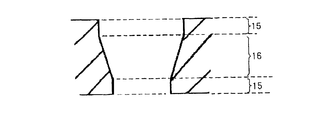
- the normal waveguide shape is such that the shape of the waveguide opening is rectangular, and the inner diameter size from the end of one waveguide to the end of the other waveguide (that is, 4 of the rectangular opening). (Side dimension) is constant.
- the waveguide shape according to the present invention is a straight shape formed from one waveguide end to a predetermined length from the other waveguide end. The portion 15 and the tapered portion 16 formed so that the inner diameter size is narrowed to the other waveguide end portion following the straight shape portion 15.
- the tapered portion 16 consists of two pairs of side surfaces that are inclined at a predetermined taper angle.
- the corner 17 in the tapered portion 16 has no roundness R and is sharp.
- the straight-shaped portion 15 includes two pairs of parallel side surfaces and four corner portions 18 formed at four corners, respectively.
- the corner portion 18 in the straight-shaped portion 15 is rounded in order to obtain easy mold release and durability of the mold. Further, the corner portion 18 may be provided with a taper so that the radius of curvature becomes larger as it approaches the tapered portion 16.
- the radius of curvature R at the portion 18a on the waveguide end side of the corner 18 is 1 mm
- the radius of curvature R at the portion 18b adjacent to the tapered portion 16 of the corner 18 is 1.5 mm.
- the tapered portion 16 and the straight portion 15 are arranged in this order with respect to the release direction (from the bottom to the top of the drawing).
- the present invention is not limited to this shape.
- the straight-shaped portion 15 and the tapered-shaped portion 16 may be arranged in this order in the release direction (from the bottom to the top of the drawing).
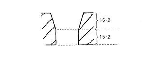
- the waveguide illustrated in FIG. 6 includes a tapered portion 16-2 formed so that the inner diameter size is narrowed to a predetermined length from one waveguide end to the other waveguide end. And a straight-shaped portion 15-2 formed with a constant inner diameter to the other waveguide end portion following the tapered-shaped portion 16-2.
- both end portions of the waveguide are formed by straight-shaped portions 15, and a portion between these straight-shaped portions 15 is formed by a tapered-shaped portion 16.
- both end portions of the waveguide are formed by the tapered portions 16 and the portion between the tapered portions 16 is formed by the straight portion 15.
- the waveguide part formed as a part of the casting ODU casing is configured by combining the straight part and the tapered part. To achieve both. In particular, by adding roundness R to the corners of the four corners with respect to the straight shape portion, the ease of release is improved.
- the tapered portion the taper angle is set to an angle that does not affect the electrical characteristics and is easy to release. As a result, both the manufacturability of the casting and the electrical characteristics of the waveguide are achieved.
- the roundness R of the corners of the four corners of the straight shape portion is also made compatible by making the radius of curvature R so as not to affect the ease of release and the electrical characteristics. If the waveguide part is designed as described above, the electrical characteristics of the waveguide part are maintained without additional processing after the casing is removed from the mold, so compared to conventional ODU casings. Manufacturing costs can be greatly reduced.
- Example 1 Further, the shape of the waveguide according to the present invention will be specifically described by taking as an example the aperture (size: 10.668 ⁇ 4.318 mm) of a rectangular waveguide of size WRJ-220 that conforms to the EIAJ standard described above.
- the corners of the waveguide are rounded R from a mechanical point of view, such as casting manufacturability.
- the roundness R is provided so that only the dimension on the long side of the tube hole is enlarged. For example, by rounding the curvature radius R of 1.5 mm at the corner of the tube hole of the rectangular waveguide of size WRJ-220, the aperture size of the rectangular waveguide is expanded to approximately 11.100 ⁇ 4.318 mm.
- an opening of the straight portion 15 is provided at one end of the waveguide shown in FIG.
- the straight-shaped part 15 is provided by fixed length from opening of this one waveguide end part.
- a tapered portion 16 is provided so that the inner diameter size becomes narrower from the straight shape portion 15 toward the other end side of the waveguide.
- the straight-shaped portion 15 is set to a pipe length of 5 mm and the tapered-shaped portion 16 is set to 15 mm.
- the corner portion 18 of the straight portion 15 is tapered so as to gradually change from a radius of curvature of 1.5R to 2R as it approaches the tapered portion 16 from the opening at one end of the waveguide (FIG. 4 ( b)).
- the tapered portion 16 is formed at a predetermined taper angle so that the inner diameter size becomes narrower toward the other waveguide end (lower side in the figure).
- the straight portion 15 has a length of about 5 mm, the influence on the castability was small. Furthermore, in this specific example, since the four corners 18 of the straight-shaped portion 15 are tapered as described above, it is easier to release.
- the change in the aperture size is reduced by the amount of shortening to 15 mm compared to the case where the taper is provided over the entire length of 20 mm of the tube hole. That is, the difference in aperture between both ends of the waveguide can be reduced.
- the taper angle is 2 °
- the taper is only 15mm, a difference of 0.524mm per side is required (difference between both: 0.176mm.
- the change of the waveguide diameter at 15mm is from 10.668 ⁇ 4.318mm to 9.62 ⁇ 3.270mm).
- FIG. 10 is a graph comparing one sample of the waveguide shape according to the present invention composed of a straight shape portion and a tapered shape portion with a waveguide shape consisting entirely of a taper with respect to electrical characteristics.
- the graph of the reflection characteristic (S11) in FIG. 10 shows that the characteristic becomes better as it goes downward. From this figure, it can be seen that the reflection characteristics of the waveguide shape according to the present invention are improved as compared with the waveguide shape which is entirely tapered. Specifically, a maximum improvement of 6 dB can be seen in the range of 13000 to 16000 MHz.
- the rounded radius R is added to the corner portion 18 of the straight-shaped portion 15 to increase the standard size of the waveguide.
- the dimension of the long side of the tube hole is slightly larger than the standard, and the influence on the waveguide characteristics such as the cut-off frequency is small.
- the rounded portion R is not sharpened at the corner portion 18 of the straight-shaped portion 15, the ease of pulling out from the mold and the durability of the mold are improved.
- the straight shape portion of this specific example maintains both the manufacturability of the casting and the electrical characteristics of the waveguide by setting the roundness of the corner 18 to about 1.5R.
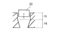
- the sliding shim is formed outwardly at a cylindrical portion 22 having an outer diameter substantially the same as the inner diameter of the waveguide portion 21 of the ODU, and at one end of the cylindrical portion 22.
- the flange portion 23 is formed.
- the sliding shim is made of a metal such as stainless steel.
- the other end of the cylindrical portion 22 of the sliding shim that is, the end portion on which the flange portion 23 is not formed becomes ODU. It is inserted from the opening 21A of the waveguide portion 21. Since the outer diameter of the cylindrical portion 22 is substantially the same as the inner diameter of the waveguide portion 21, the cylindrical portion 22 can be slid within the waveguide portion 21.
- the waveguide portion 21 on the ODU side and the waveguide portion 24 on the antenna side are aligned, and the end face 25 of the waveguide portion 24 contacts the flange portion 23 of the sliding shim.
- the waveguide portion 24 is pressed against the waveguide portion 21, and the cylindrical portion 22 of the sliding shim is completely inserted into the waveguide portion 21.
- the waveguide portions 21 and 24 are fastened using bolts or the like. As a result, the gap formed between the end faces 25 and 26 of the connected waveguide portions 21 and 24 is closed by the cylindrical portion 22 of the sliding shim, so that the reflection loss at the waveguide connection portion is reduced.
- the waveguide shape according to the present invention has good affinity with such a sliding shim. This is described in detail below.
- the cylindrical portion 22 of the shim When the sliding shim is used in combination with a rectangular waveguide having a tapered tube hole as shown in FIG. 9B, the cylindrical portion 22 of the shim has a tube hole as shown in FIG. May interfere with the inner wall 28 and cannot be inserted into the waveguide portion. Considering this, as shown by an arrow in FIG. 12B, the diameter of the opening 27 of the waveguide portion is enlarged so that the cylindrical portion 22 can be inserted without interfering with the inner wall 28. There is a need. This is a major limitation in design.
- either one end of the waveguide shape is formed of a straight shape portion. Therefore, the above problems can be avoided by using a sliding shim on the straight shape portion side.
- the straight portion 15 of the waveguide shape according to the present invention is matched to the range in which the cylindrical portion 22 of the sliding shim is inserted into and removed from the tube hole of the waveguide portion. It is good to let it. As a result, a difference in clearance from the inner wall of the waveguide hole of the waveguide does not occur depending on the amount of shim insertion, and a large characteristic change can be suppressed.
- the casting accuracy of both portions can be made differently.
- a high casting accuracy is required for the straight-shaped portion 15 into which a sliding shim is inserted in order to suppress characteristic deterioration due to a shim assembly error.
- the taper-shaped portion 16 into which the shim is not inserted needs only to ensure the characteristics as a waveguide, so that high casting accuracy is not necessary.
- a waveguide shape having a tube hole with only a taper if it is attempted to increase the accuracy, it must be performed over the entire length. Production is possible.
- the sliding shim is used for a rectangular waveguide with a diameter conforming to the EIAJ standard (hereinafter referred to as a standard waveguide)
- the outer diameter of the shim cylindrical portion must be smaller than the diameter of the standard waveguide. I must. Accordingly, the inner diameter dimension of the shim cylindrical portion is shifted from the diameter conforming to the EIAJ standard by the thickness of the side wall of the shim cylindrical portion, and the electrical characteristics are deteriorated.
- the side opposite to the side where the cylindrical portion 22 of the sliding shim is inserted is shown.
- the aperture size of the straight portion 15 so that the standard waveguide aperture 30 on the side and the aperture 29 of the shim cylindrical portion 22 are the same.
- the tapered portion 16 so that the diameter of the narrowed tip is the standard waveguide diameter 30.
- the larger one of the diameters at both ends of the waveguide is an actual passage opening in which the diameter 29 of the shim cylindrical portion 22 has the same size as the standard waveguide diameter 30, and the other end is also the same. Since the standard waveguide aperture is 30, both apertures are electrically the size of the standard waveguide.
- the waveguide shape of the present application comprising the straight shape portion and the taper shape portion, when combined with the sliding shim, the mutual weak points can be complemented, and the compatibility is very good.
- the waveguide portion particularly the outer portion of the ODU casing will be described.
- the surface of a metal housing that contains precision electronic components such as transmitter / receiver circuits is usually coated with resin in consideration of durability and corrosion resistance. .
- Such coating can increase the reliability of the equipment by delaying the progress of the corrosion of the metal casing forming the ODU.
- the paint color is set to white, the metal casing is prevented from absorbing sunlight, and there is an effect that heat is not easily propagated inside the ODU. Such painting was expensive.
- Casting an ODU casing can reduce mass production and reduce costs, but the cast casing can be used as a hot-flow pattern or mold trace on the surface of the outer appearance when it is removed from the mold. Has occurred.
- the present applicant has found the invention modes described below.
- the following second embodiment is also applied to a housing having a waveguide portion according to the first embodiment.
- FIG. 16 is a perspective view showing a state in which the ODU according to the second embodiment is installed.
- the ODU 31 of this embodiment shown in this figure includes a transmission unit (not shown) that transmits a radio signal, a reception unit (not shown) that receives a radio signal, and a housing that accommodates at least these.
- an antenna 33 is assembled to the ODU 31 as an example.
- the antenna 33 transmits a radio signal from the transmission unit to the outside and receives a radio signal to the reception unit from the outside.
- the ODU 31 includes a joint unit (see reference numeral 35 in FIG. 18) that connects the antenna 33. Have.
- the ODU 31 is fixed by being attached to, for example, a pole 34 standing on the roof of the building.
- FIG. 17 shows the ODU 31, (a) is a front view, and (b) is a rear view.
- 18A is a perspective view showing the front side of the ODU 31
- FIG. 18B is a perspective view showing the back side of the ODU 31.
- the casing of the ODU 31 shown in these drawings is configured by combining a cover 31A and a case 31B. Further, a transmitter and a receiver are accommodated in the housing. Further, the ODU 31 is provided with a handle 36 so that it is easy to carry and further facilitates setting of the transmission / reception direction.
- the handle 36 may be formed integrally with the case 31B. When the housing and the handle 36 are integrally formed, the number of parts can be reduced.
- Such a casing is made of non-ferrous metal.
- the casing portion may be manufactured by cutting, but when the ODU 31 casing is mass-produced, it is formed by a die casting method.
- a non-ferrous metal is used as the material of the casing. Examples thereof include aluminum, aluminum alloy (aluminum alloy), and zinc alloy. These non-ferrous metals are lightweight, easy to process, and particularly easy to mold by the die casting method, and are therefore suitable as a housing for ODU31. Molding by the die casting method facilitates mass production and reduces costs.
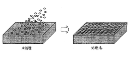
- the outer surface of the ODU casing is not coated in the present invention, and the powder is uniformly sprayed on the surface of the non-ferrous metal at high speed, and the unevenness is continuous over the entire surface of the non-ferrous metal. Formed.
- the unevenness is a collision mark. Concavities and convexities were similarly formed on the surface of the non-ferrous metal forming the handle 36.
- the handle 36 is formed integrally with the housing, the housing and the handle can be processed at a time, which is efficient.
- FIG. 19 shows how the unevenness is formed in this way.
- stainless steel, glass beads, or aluminum oxide (alumina) powder can be used.
- a powder injection device a rotary blade type (impeller type) or air nozzle type shot peening device can be used.
- Such a high temperature is momentarily applied to the surface of the aluminum alloy having a melting point of around 700 ° C., so that it is expected that fine remelting occurs in the surface layer of the aluminum alloy. The same is expected to occur even for non-ferrous metals having a melting point of 1000 ° C. or less, such as aluminum (melting point: 660 ° C.) or zinc alloy (around 600 ° C.).
- FIG. 20 is a cross-sectional view schematically showing the outer surface and the inside of a non-ferrous metal having irregularities formed in this way. As shown in this figure, irregularities 32a are formed on the outer surface of the non-ferrous metal 32, and the outer surface is modified into an oxide layer 32b by remelting.
- the outer surface of the aluminum alloy mainly contains aluminum oxide (Al 2 O 3 ).
- An oxide film is formed.
- Such oxides themselves have high corrosion resistance.
- the oxide film formed on the surface by the powder collision is thicker than the oxide film formed by naturally oxidizing the surface.
- the outer surface layer of the aluminum alloy is refined by the action of rapid heating and quenching, and this results in a denser metal structure than inside the aluminum alloy, thus improving the corrosion resistance of the ODU1 housing. To do.
- the oxide alloy formed on the surface of the base material has higher hardness than the base material, it can be expected that the wear resistance and scratch resistance are also improved.
- the injection of stainless steel powder forms irregularities consisting of continuous collision marks over the entire surface of the housing, and the surface roughness due to these irregularities prevents fingerprints from adhering to the metal housing surface.
- Ra center line average roughness
- the average diameter of the recesses having the surface roughness in this range is about several hundred ⁇ m.
- a hard, fine powder collides at high speed with the outer surface of the non-ferrous metal casing, and the outer surface layer of the non-ferrous metal casing is modified by using the heat generated at that time. It is quality. Therefore, other than non-aluminum alloys, other non-ferrous metals having a relatively low melting point (for example, about 1000 ° C. or less) can be expected to form metal oxides on the surface due to the same action. Can be used for
- the modified housing surface is denser than the metal structure inside the non-ferrous metal forming the housing 32, and the oxide film is formed thicker than the natural film. . Therefore, corrosion resistance and durability were improved as compared with non-surface-treated non-ferrous metals (see FIGS. 21 and 22). Therefore, it has excellent environmental resistance as the casing 2 that accommodates the transmission / reception circuit of the ODU 1 installed outdoors where the installation environment is very severe.
- FIG. 21 shows the housing surface before and after 192 hours in the corrosive gas test.
- the specification of this corrosive gas test conforms to the standard of IEC 61587-1.
- the surface of the ODU 31 housing is formed with a surface on which the powder collides and a surface that does not collide, and sulfur dioxide gas (SO 2 concentration: 25 ppm) is formed on the surface of the housing.
- SO 2 concentration: 25 ppm sulfur dioxide gas
- the environmental temperature in this test is 40 ° C., and the environmental humidity is 80% RH.
- the powder impingement surface was hardly discolored compared to the powder non-impact surface (see FIG. 21B).
- FIG. 22 shows the case surface before and after 120 hours in the salt spray test.
- the specifications for this salt spray test conform to IEC 60068-2-11.
- a surface on which the powder collides with a surface of the casing of the ODU 31 is formed, and a surface where the powder does not collide is formed. And continuously sprayed for 120 hours. Even after 120 hours in such a salt spray test, the powder impingement surface was hardly discolored compared to the powder non-impact surface (see FIG. 22B).
- the casing surface has such excellent corrosion resistance and durability, expensive coating on the casing surface is not required. Since there is no need for painting work using organic solvents, it is possible to provide a housing that is environmentally friendly.
- the surface of the casing can be made to have a surface roughness Ra on which fingerprints are difficult to adhere.
- the surface of the housing is increased due to the impact of the powder and the surface area is increased. At the same time, the housing surface is exposed without being coated with resin, so that the heat dissipation of the housing can also be improved. .
- FIG. 23A a hot water flow pattern
- FIG. 23B and FIG. 23C The housing surface (see FIG. 23B and FIG. 23C) formed in FIG. FIG. 23 (a) shows a photograph of the casing surface of the cast product in which a molten metal flow pattern is generated, and FIG.
- FIG. 23 (b) shows a case where minute irregularities due to collision marks are uniformly formed on the casing surface.
- a photograph of the housing surface (same magnification as in FIG. 23A) is shown.
- FIG.23 (c) has shown the enlarged photograph (50 times) of the part enclosed with the circle of FIG.23 (b).
- (Application example) 24 is a block diagram illustrating an example of a wireless communication system including a wireless transmission / reception apparatus (ODU) according to the present invention.
- FIG. 25 is a block diagram illustrating an example of a circuit accommodated in the wireless transmission / reception apparatus of FIG. FIG.
- an A station 41 (B station 51) inputs and outputs a single baseband signal and modulates and demodulates the baseband signal, an ODU43 (53) that is a radio transceiver, One coaxial cable 45 (55) that interfaces between the IDU 42 (52) and the ODU 43 (53), and an antenna 44 (54) that is connected to the ODU 43 (53) and transmits and receives wirelessly between opposite stations.
- the ODU 43 (53) of the A station 41 (B station 51) includes a multiplexer circuit 61, a transmission / reception circuit 62, and a control circuit 63 as shown in FIG.
- the transmission / reception circuit 62 in which the transmission circuit and the reception circuit are integrated is mounted.
- the transmission circuit and the reception circuit may be provided separately.
- the multiplexer circuit 61 of the ODU 43 separates multiplexed signals input from the IDU side via the coaxial cable 45 (55), supplies DC power to each circuit, and outputs a control signal to the control circuit 63. It has a function.
- the multiplexer circuit 61 further has a function of separating and extracting the modulated wave and outputting it to the transmission / reception circuit 62 and a function of outputting the demodulation intermediate frequency signal input from the transmission / reception circuit 62 to the IDU.
- the transmission / reception circuit 62 of the ODU 43 (53) converts the modulated wave input from the multiplexer circuit 61 into a radio frequency signal and transmits it from the antenna 44 (54), and the radio frequency signal received by the antenna 44 (54). Is converted into an intermediate frequency signal for demodulation and output to the multiplexer circuit 61.
- the control circuit 33 of the ODU 43 (53) has a function of performing communication control between IDU and ODU and a function of monitoring the control of the ODU 43 (53).
- the multiplexed signal input from the IDU 42 (52) to the ODU 43 (53) is separated into a DC power source, a control signal, and a modulated wave by the multiplexer circuit 61. Is output.
- the modulated wave input to the transmission / reception circuit 62 is converted into a radio frequency signal (RF signal) by the transmission / reception circuit 62 and transmitted to the opposite station via the antenna 44 (54).
- the RF signal received from the opposite station by the antenna 44 (54) is converted into an intermediate frequency signal for demodulation by the transmission / reception circuit 62, and output to the IDU 42 (52) via the multiplexer circuit 61 and the coaxial cable 45 (55).
- the example shown in FIG. 24 is a configuration in which the IDU and the ODU are separated in one base station, but the present invention can also be applied to a case where the IDU and the ODU are integrated.
- Precision electronic components such as a multiplexer circuit 61, a transmission / reception circuit 62, and a control circuit 63 that enable the above-described operation are accommodated in the housing of the ODU 31 shown in FIGS.
- the casing of the ODU according to the present invention has an outer surface excellent in environmental resistance even if it is not painted. Therefore, the above electronic circuit can be securely protected in a harsh outdoor environment.
Landscapes
- Engineering & Computer Science (AREA)
- Manufacturing & Machinery (AREA)
- Computer Networks & Wireless Communication (AREA)
- Signal Processing (AREA)
- Waveguides (AREA)
- Waveguide Aerials (AREA)
- Waveguide Connection Structure (AREA)
Abstract
Description
12 ODUの筐体
13 テーパー部分の斜面
14 ドリル
15 ストレート形状部分
16 テーパー形状部分
17、18 角部
21 ODU側の導波管部分
21A 導波管部分21の開口部
22 スライド式シムの筒状部
23 スライド式シムのフランジ部
24 アンテナ側の導波管部分
25 導波管部分24の端面
26 導波管部分21の端面
27 スライド式シムが挿入される導波管部分の開口部
28 導波管の管穴の内壁
29 スライド式シムの筒状部の口径
30 標準導波管の口径
31 屋外用無線送受信装置(ODU)
31A カバー
31B ケース
32 非鉄系金属
32a 凹凸
32b 酸化層
33 アンテナ
34 ポール
35 ジョイント部
36 取っ手
41 A局(基地局)
42、52 IDU
43、53 ODU
44、54 アンテナ
45、55 同軸ケーブル
51 B局(基地局)
61 マルチプレクサ回路
62 送受信回路
63 制御回路
まず、ODUの導波管部分に関して述べる。
さらに、本発明による導波管形状について、前述したEIAJ規格に準ずるサイズWRJ-220の矩形導波管の口径(サイズ;10.668×4.318mm)を例にして具体的に説明する。
次に、本発明による導波管形状をより効果的に利用できる他の具体例を挙げる。
(第二の実施形態)
次に、上記導波管部分の他の部分、特にODU筐体の外側部分に関して述べる。
図24は本発明に係る無線送受信装置(ODU)を備えた無線通信システムの一例を示したブロック図であり、図25は図24の無線送受信装置内に収容される回路の例を示したブロック図である。
Claims (19)
- 屋外に設置される通信装置であって、
信号を送信する送信部と、信号を受信する受信部と、外部のアンテナと接続して信号の送受を行う導波管と、該送信部および該受信部を収容する筐体とを備えており、
前記導波管は前記筐体と一体で形成されており、かつ、前記導波管の管穴の一部にテーパーが設けられている、通信装置。 - 前記テーパーにおいて前記導波管の管穴が所定の角度で傾斜している、請求項1に記載の通信装置。
- 前記テーパーは前記導波管の内径サイズが、前記導波管の一方の端部に向かって狭くなるように形成されている、請求項1に記載の通信装置。
- 前記導波管の少なくとも一方の端部から所定の距離において、前記導波管の内径サイズが一定の寸法になるよう形成されている、請求項1乃至3のいずれか1項に記載の通信装置。
- 屋外に設置される通信装置であって、
信号を送信する送信部と、信号を受信する受信部と、外部のアンテナと接続して信号の送受を行う導波管と、該送信部および該受信部を収容する筺体とを備えており、
前記導波管は前記筺体と一体で形成されており、かつ、該導波管の一方の端部から他方の端部までの内径サイズが一定の寸法からなるストレート形状部分と、所定の角度で傾斜するテーパー形状部分とを含む、通信装置。 - 前記ストレート形状部分は、四隅を成す2対の平行な側面と、該四隅にそれぞれ形成される4つの角部とからなり、該角部については、丸みRが付けられており、
前記テーパー形状部分は所定のテーパー角度で傾斜した2対の側面からなる、請求項5に記載の通信装置。 - 前記ストレート形状部分の前記角部には、前記テーパー形状部分に近くなるに従って曲率半径が大きくなるように前記丸みRが設けられている、請求項6に記載の通信装置。
- 前記ストレート形状部分が前記導波管の一端から他端への所定の長さまで形成され、前記テーパー形状部分が前記ストレート形状部分に続いて前記導波管の他端まで口径が狭くなるように形成されている、請求項5乃至7のいずれか1項に記載の通信装置。
- 前記テーパー形状部分が前記導波管の一端から他端への所定の長さまで口径が狭くなるように形成され、前記ストレート形状部分が前記テーパー形状部分に続いて前記導波管の他端まで一定の口径で形成されている、請求項5乃至7のいずれか1項に記載の通信装置。
- 前記ストレート形状部分および前記テーパー形状部分の少なくとも一方が導波管部分の長さ方向において2段以上設けられている、請求項5乃至9のいずれか1項に記載の通信装置。
- アンテナに備わる導波管部分と前記導波管とを接続するシムをさらに備え、前記シムは前記導波管の管穴にスライド可能に挿入される筒状部を有し、
前記導波管は前記筒状部が挿入される側に前記ストレート形状部分を備えている、請求項5乃至10のいずれか1項に記載の通信装置。 - 前記導波管における前記シムが挿入される範囲が前記ストレート形状部分で構成されている、請求項11に記載の通信装置。
- 前記シムの筒状部の内径寸法が、前記シムが挿入される側とは反対側の前記導波管の端部の口径寸法と略同一である、請求項11または12に記載の通信装置。
- 屋外に設置される通信装置であって、
信号を送信する送信部と、信号を受信する受信部と、外部のアンテナと接続して信号の授受を行う導波管と、該送信部および該受信部を収容する筐体とを備えており、
前記導波管は前記筐体と一体で形成されており、
前記筐体の外側表面は、塗装せずに凹凸処理されている、通信装置。 - 前記導波管の管穴の一部にテーパーが設けられている、請求項14に記載の通信装置。
- 前記テーパーにおいて前記導波管の管穴が所定の角度で傾斜している、請求項15に記載の通信装置。
- 前記テーパーは前記導波管の内径サイズが、前記導波管の一方の端部に向かって狭くなるように形成されている、請求項15に記載の通信装置。
- 前記ストレート形状部分が前記導波管の少なくとも一方の端部に形成されている、請求項15または16に記載の通信装置。
- 前記導波管の少なくとも一方の端部から所定の距離において、前記導波管の内径サイズが一定の寸法になるよう形成されている、請求項15乃至18のいずれか1項に記載の通信装置。
Priority Applications (6)
| Application Number | Priority Date | Filing Date | Title |
|---|---|---|---|
| JP2012536308A JP5549738B2 (ja) | 2010-09-29 | 2011-09-07 | 通信装置 |
| CN201180045815.6A CN103155272B (zh) | 2010-09-29 | 2011-09-07 | 通信装置 |
| EP11828736.6A EP2624359A4 (en) | 2010-09-29 | 2011-09-07 | COMMUNICATION DEVICE |
| US13/824,136 US9166278B2 (en) | 2010-09-29 | 2011-09-07 | Communication apparatus |
| KR1020137007664A KR101465922B1 (ko) | 2010-09-29 | 2011-09-07 | 통신 장치 |
| BR112013006739A BR112013006739A2 (pt) | 2010-09-29 | 2011-09-07 | aparelho de comunicação instalado no exterior |
Applications Claiming Priority (2)
| Application Number | Priority Date | Filing Date | Title |
|---|---|---|---|
| JP2010-219081 | 2010-09-29 | ||
| JP2010219081 | 2010-09-29 |
Publications (1)
| Publication Number | Publication Date |
|---|---|
| WO2012043175A1 true WO2012043175A1 (ja) | 2012-04-05 |
Family
ID=45892648
Family Applications (1)
| Application Number | Title | Priority Date | Filing Date |
|---|---|---|---|
| PCT/JP2011/070360 WO2012043175A1 (ja) | 2010-09-29 | 2011-09-07 | 通信装置 |
Country Status (7)
| Country | Link |
|---|---|
| US (1) | US9166278B2 (ja) |
| EP (1) | EP2624359A4 (ja) |
| JP (1) | JP5549738B2 (ja) |
| KR (1) | KR101465922B1 (ja) |
| CN (1) | CN103155272B (ja) |
| BR (1) | BR112013006739A2 (ja) |
| WO (1) | WO2012043175A1 (ja) |
Families Citing this family (2)
| Publication number | Priority date | Publication date | Assignee | Title |
|---|---|---|---|---|
| US9743383B1 (en) * | 2015-02-24 | 2017-08-22 | The Directv Group, Inc. | Hybrid wireless-wireline communications system and method |
| WO2020014452A1 (en) | 2018-07-12 | 2020-01-16 | Abilene Christian University | Apparatus, systems, and methods for non-invasive measurement of flow in a high temperature pipe |
Citations (5)
| Publication number | Priority date | Publication date | Assignee | Title |
|---|---|---|---|---|
| JPH09139603A (ja) * | 1995-11-13 | 1997-05-27 | Matsushita Electric Ind Co Ltd | 円偏波一直線偏波変換器 |
| JPH11284428A (ja) * | 1998-03-30 | 1999-10-15 | New Japan Radio Co Ltd | パラボラアンテナ給電用一次放射器 |
| JP2000332524A (ja) * | 1999-05-17 | 2000-11-30 | Alps Electric Co Ltd | 衛星放送受信用コンバーター |
| JP2001156501A (ja) * | 1999-11-29 | 2001-06-08 | Nec Corp | 導波管接続方法および接続構造 |
| JP2002151921A (ja) * | 2000-11-09 | 2002-05-24 | Mitsubishi Electric Corp | 偏波角切替調整装置 |
Family Cites Families (26)
| Publication number | Priority date | Publication date | Assignee | Title |
|---|---|---|---|---|
| GB696900A (en) | 1950-07-06 | 1953-09-09 | Sydney Robson | Improvements in waveguides and aerials |
| CA1274327A (en) * | 1985-02-22 | 1990-09-18 | Masao Momose | Microwave transmitter/receiver apparatus |
| JPS61214802A (ja) * | 1985-03-20 | 1986-09-24 | Fujitsu Ltd | 無線装置 |
| US4792814A (en) * | 1986-10-23 | 1988-12-20 | Mitsubishi Denki Kabushiki Kaisha | Conical horn antenna applicable to plural modes of electromagnetic waves |
| JPH03248760A (ja) * | 1990-02-27 | 1991-11-06 | Toshiba Corp | 金属部品の製造方法 |
| JP2759900B2 (ja) | 1993-06-30 | 1998-05-28 | 日本アンテナ株式会社 | ホーン一体型円偏波・直線偏波変換器 |
| US5760749A (en) * | 1994-03-17 | 1998-06-02 | Fujitsu Limited | Antenna integral-type transmitter/receiver system |
| JP3644104B2 (ja) | 1995-12-20 | 2005-04-27 | 株式会社村田製作所 | 誘電体共振器 |
| JP2000031702A (ja) | 1998-07-14 | 2000-01-28 | Alps Electric Co Ltd | 衛星放送受信用コンバータ |
| JP2001036301A (ja) | 1999-07-23 | 2001-02-09 | Alps Electric Co Ltd | 円導波管 |
| US6272269B1 (en) * | 1999-11-16 | 2001-08-07 | Dn Labs Inc. | Optical fiber/waveguide illumination system |
| JP2001168611A (ja) | 1999-12-13 | 2001-06-22 | Nec Wireless Networks Ltd | 屋外設置用無線送受信装置のアンテナと送受信装置との導波管接続構造 |
| JP4052621B2 (ja) * | 2000-08-11 | 2008-02-27 | 株式会社東芝 | 無線通信装置のゲイン調整器、無線通信装置のゲイン調整方法、及び無線通信システムの加入者局送信レベル制御方法 |
| JP3769494B2 (ja) | 2001-05-17 | 2006-04-26 | シャープ株式会社 | 偏波分離構造、電波受信用コンバータおよびアンテナ装置 |
| JP3899256B2 (ja) * | 2001-12-10 | 2007-03-28 | シャープ株式会社 | 衛星放送用アンテナの円偏波受信用コンバータ |
| JP4462043B2 (ja) | 2005-01-14 | 2010-05-12 | 日本電気株式会社 | マイクロ波無線通信システム |
| JP4229927B2 (ja) | 2005-04-27 | 2009-02-25 | シャープ株式会社 | 偏波分離構造、低雑音コンバータおよびアンテナ装置 |
| CN101010448B (zh) | 2005-06-23 | 2010-09-29 | 东京毅力科创株式会社 | 半导体处理装置用的构成部件及其制造方法 |
| JP2007142184A (ja) * | 2005-11-18 | 2007-06-07 | Sharp Corp | 電波受信用コンバータ |
| US7511678B2 (en) * | 2006-02-24 | 2009-03-31 | Northrop Grumman Corporation | High-power dual-frequency coaxial feedhorn antenna |
| JP4862530B2 (ja) * | 2006-07-25 | 2012-01-25 | 日本電気株式会社 | 導波管 |
| US7893789B2 (en) | 2006-12-12 | 2011-02-22 | Andrew Llc | Waveguide transitions and method of forming components |
| US7755557B2 (en) * | 2007-10-31 | 2010-07-13 | Raven Antenna Systems Inc. | Cross-polar compensating feed horn and method of manufacture |
| KR20100058337A (ko) * | 2008-11-24 | 2010-06-03 | 삼성전자주식회사 | 휴대용 전자 기기의 도장 조성물 및 그의 도장방법 |
| CN101807930A (zh) | 2009-02-13 | 2010-08-18 | 华为技术有限公司 | 基站射频双工器、射频模块和射频系统 |
| EP2587902A1 (en) * | 2010-06-25 | 2013-05-01 | Nec Corporation | Communications device and production method for communications device case |
-
2011
- 2011-09-07 EP EP11828736.6A patent/EP2624359A4/en not_active Withdrawn
- 2011-09-07 KR KR1020137007664A patent/KR101465922B1/ko not_active IP Right Cessation
- 2011-09-07 US US13/824,136 patent/US9166278B2/en not_active Expired - Fee Related
- 2011-09-07 WO PCT/JP2011/070360 patent/WO2012043175A1/ja active Application Filing
- 2011-09-07 CN CN201180045815.6A patent/CN103155272B/zh not_active Expired - Fee Related
- 2011-09-07 JP JP2012536308A patent/JP5549738B2/ja not_active Expired - Fee Related
- 2011-09-07 BR BR112013006739A patent/BR112013006739A2/pt not_active IP Right Cessation
Patent Citations (5)
| Publication number | Priority date | Publication date | Assignee | Title |
|---|---|---|---|---|
| JPH09139603A (ja) * | 1995-11-13 | 1997-05-27 | Matsushita Electric Ind Co Ltd | 円偏波一直線偏波変換器 |
| JPH11284428A (ja) * | 1998-03-30 | 1999-10-15 | New Japan Radio Co Ltd | パラボラアンテナ給電用一次放射器 |
| JP2000332524A (ja) * | 1999-05-17 | 2000-11-30 | Alps Electric Co Ltd | 衛星放送受信用コンバーター |
| JP2001156501A (ja) * | 1999-11-29 | 2001-06-08 | Nec Corp | 導波管接続方法および接続構造 |
| JP2002151921A (ja) * | 2000-11-09 | 2002-05-24 | Mitsubishi Electric Corp | 偏波角切替調整装置 |
Non-Patent Citations (1)
| Title |
|---|
| See also references of EP2624359A4 * |
Also Published As
| Publication number | Publication date |
|---|---|
| EP2624359A4 (en) | 2015-05-06 |
| CN103155272A (zh) | 2013-06-12 |
| KR20130055666A (ko) | 2013-05-28 |
| US9166278B2 (en) | 2015-10-20 |
| KR101465922B1 (ko) | 2014-11-26 |
| JPWO2012043175A1 (ja) | 2014-02-06 |
| BR112013006739A2 (pt) | 2016-06-14 |
| JP5549738B2 (ja) | 2014-07-16 |
| CN103155272B (zh) | 2015-04-15 |
| US20130181872A1 (en) | 2013-07-18 |
| EP2624359A1 (en) | 2013-08-07 |
Similar Documents
| Publication | Publication Date | Title |
|---|---|---|
| WO2011162281A1 (ja) | 通信装置および、通信装置の筐体の製造方法 | |
| JP5549738B2 (ja) | 通信装置 | |
| JP5698253B2 (ja) | アンテナ装置およびアンテナ選択方法 | |
| EP1375034A3 (en) | Method and apparatus for directional solidification of a metal melt | |
| US20190319370A1 (en) | Welding base for a microwave device and microwave device | |
| US20180177057A1 (en) | Gold-plating etching process for 5g communication high-frequency signal boards | |
| CN104345414B (zh) | 模块回退式安装卸载装置 | |
| FI123372B (fi) | Menetelmä metallurgisen uunin yhteydessä käytettävän jäähdytyselementin päällystämiseksi metallipäällysteellä ja jäähdytyselementti | |
| US20110241952A1 (en) | Antenna Apparatus with a Modified Surface | |
| CN106132137B (zh) | 一种壳体的净空区域的加工方法、壳体和移动终端 | |
| CN106984806A (zh) | 一种用于手机天线触点的金属混合粉末及触点加工方法 | |
| CN101959395A (zh) | 屏蔽壳体及其表面处理方法 | |
| CN203166069U (zh) | 车载天线 | |
| CN113414364B (zh) | 一种固态双金属内壁耐磨物料输送圆管及其制备方法 | |
| CN106381827B (zh) | 微波融雪设备 | |
| CN201000788Y (zh) | 一种综合电缆 | |
| CN111391223A (zh) | 基于熔接技术的接收器外壳的制造工艺 | |
| CN216485480U (zh) | 一种雷达的保护装置及雷达 | |
| CN215954907U (zh) | 一种通讯设备用屏蔽式电缆 | |
| US20230259179A1 (en) | Housings for electronic devices | |
| CN202711853U (zh) | 超轻型同轴电缆 | |
| WO2023169429A1 (zh) | 一种结构件及其制备方法和电子设备 | |
| CN105062367A (zh) | 电气接点测温装置外表面耐磨涂层 | |
| CN208226076U (zh) | 一种微波通信用天线装置 | |
| KR101892027B1 (ko) | 내장형 rf 안테나를 구비한 dtg 장치 |
Legal Events
| Date | Code | Title | Description |
|---|---|---|---|
| WWE | Wipo information: entry into national phase |
Ref document number: 201180045815.6 Country of ref document: CN |
|
| 121 | Ep: the epo has been informed by wipo that ep was designated in this application |
Ref document number: 11828736 Country of ref document: EP Kind code of ref document: A1 |
|
| WWE | Wipo information: entry into national phase |
Ref document number: 13824136 Country of ref document: US |
|
| REEP | Request for entry into the european phase |
Ref document number: 2011828736 Country of ref document: EP |
|
| WWE | Wipo information: entry into national phase |
Ref document number: 2011828736 Country of ref document: EP |
|
| ENP | Entry into the national phase |
Ref document number: 2012536308 Country of ref document: JP Kind code of ref document: A Ref document number: 20137007664 Country of ref document: KR Kind code of ref document: A |
|
| NENP | Non-entry into the national phase |
Ref country code: DE |
|
| REG | Reference to national code |
Ref country code: BR Ref legal event code: B01A Ref document number: 112013006739 Country of ref document: BR |
|
| ENP | Entry into the national phase |
Ref document number: 112013006739 Country of ref document: BR Kind code of ref document: A2 Effective date: 20130325 |