WO2012033136A1 - インダクタを含む積層型電子部品 - Google Patents
インダクタを含む積層型電子部品 Download PDFInfo
- Publication number
- WO2012033136A1 WO2012033136A1 PCT/JP2011/070399 JP2011070399W WO2012033136A1 WO 2012033136 A1 WO2012033136 A1 WO 2012033136A1 JP 2011070399 W JP2011070399 W JP 2011070399W WO 2012033136 A1 WO2012033136 A1 WO 2012033136A1
- Authority
- WO
- WIPO (PCT)
- Prior art keywords
- inductor
- laminate
- wiring layer
- conductor
- inductor conductor
- Prior art date
- Legal status (The legal status is an assumption and is not a legal conclusion. Google has not performed a legal analysis and makes no representation as to the accuracy of the status listed.)
- Ceased
Links
Images














Classifications
-
- H—ELECTRICITY
- H01—ELECTRIC ELEMENTS
- H01F—MAGNETS; INDUCTANCES; TRANSFORMERS; SELECTION OF MATERIALS FOR THEIR MAGNETIC PROPERTIES
- H01F17/00—Fixed inductances of the signal type
- H01F17/0006—Printed inductances
- H01F17/0013—Printed inductances with stacked layers
-
- H—ELECTRICITY
- H01—ELECTRIC ELEMENTS
- H01F—MAGNETS; INDUCTANCES; TRANSFORMERS; SELECTION OF MATERIALS FOR THEIR MAGNETIC PROPERTIES
- H01F17/00—Fixed inductances of the signal type
- H01F17/0006—Printed inductances
- H01F2017/004—Printed inductances with the coil helically wound around an axis without a core
Definitions
- the present invention relates to a multilayer electronic component including an inductor, and more particularly to a technique for forming an inductor inside a multilayer body without using a connection conductor that penetrates an insulating layer such as a through hole.
- Inductors are used for various purposes such as high-frequency LC filter circuits, resonant circuits, and impedance matching.
- an inductor may be formed inside the ceramic laminate to form various electronic components and electronic modules.
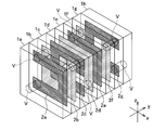
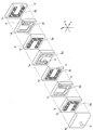
- FIG. 28 to FIG. 29 show an example of a conventional inductor formed inside such a laminate.
- 2f, 2g are connected by a through-type connection conductor V such as a through-hole, whereby an inductor having a spiral shape as a whole is formed inside the multilayer body.
- the conductor patterns 2a to 2g of the respective wiring layers are formed, for example, by printing a conductive paste on the surface of the ceramic green sheets 1b to 1h, and the plurality of green sheets 1b to 1h are stacked to form a chip and then fired. Thus, an electronic component is obtained.
- Patent Document 1 Japanese Patent Application Laid-Open No. 10-106838
- Patent Document 2 Japanese Patent Application Laid-Open No. 2009-170737
- inductor conductors printed on each wiring layer pass through a ceramic layer (green sheet). It is necessary to electrically connect through through holes. For this reason, the inductor cannot be formed only by a printing process, and a process for drilling a through hole or filling a conductive paste in the hole is required separately, which makes it difficult to make the manufacturing process complicated.
- a conventional coil-shaped inductor using through-holes is composed of upper and lower conductor patterns constituting the inductor and through-holes connecting them, and these are discontinuous through-holes as inductor conductors (pattern conductors).
- pattern conductors pattern conductors
- an object of the present invention includes an inductor by enabling an inductor to be formed across a plurality of layers within a multilayer body without using a through-insulating connection conductor such as a through hole. It is in the point which simplifies the manufacturing process of a laminated type electronic component, and improves an electrical property further.
- a first multilayer electronic component includes a first laminate having two or more wiring layers laminated via an insulating layer, and at least one insulating layer.
- a laminated electronic component comprising a second laminated body having a layer and a wiring layer formed on the surface thereof and joined to the first laminated body, wherein the wiring layer of the first laminated body and the second laminated body
- the first laminated body includes a first inductor conductor disposed in a first wiring layer of the two or more wiring layers, and the two or more wiring layers.
- a second inductor conductor disposed on the second wiring layer, wherein the first laminated conductor and the second inductor conductor form a coil-shaped inductor. The end of the first inductor conductor at the joint surface with the first laminate Having a connection conductor for electrically connecting the end portion of the second inductor conductor and.
- a plurality of inductor conductors arranged in different wiring layers inside the multilayer body are electrically connected to constitute a coil-shaped inductor.
- the first laminate is arranged so that the wiring layer and the wiring layer of the laminate (first laminate) are substantially orthogonal to each other.
- the inductor conductors are connected to each other by a second laminated body joined to the body.
- the second laminate has a wiring layer on the surface to be a joint surface with the first laminate, and the connection conductor (pattern conductor) for connecting the inductor conductors is formed on the wiring layer. Then, by connecting the end portion of the first inductor conductor and the end portion of the second inductor conductor to the connection conductor, respectively, the first inductor conductor and the second inductor conductor are connected via the connection conductor. Connect them electrically.
- connection conductor provided in the second laminate may be formed by, for example, a method such as printing a conductive paste. According to the present invention having such a structure, a through hole drilling process or a hole that has been conventionally required There is no need to fill the inside with the conductive paste.
- the inductor can be configured only by the conductor pattern formed on the surface of the insulating layer, and a high-Q and low-loss inductor can be provided inside the multilayer body.
- the first multilayer body has an overall shape of a rectangular parallelepiped, and the first inductor conductor is formed in a loop shape in the first wiring layer. One end portion and the other end portion are exposed at the joint surface with the second laminate, and the second inductor conductor is looped so as to substantially overlap the first inductor conductor in the second wiring layer.
- the one end part is exposed at the joint surface with the second laminate and the lamination direction of the first laminate (when viewed from the direction perpendicular to each wiring layer of the first laminate / Similarly, the first inductor is disposed at a position substantially overlapping with one end of the first inductor conductor, and the other end is exposed at the joint surface with the second stacked body and the first stacked body in the stacking direction. Approximately the same weight as the other end of the inductor conductor Arranged that position, the connecting conductor, and the other end portion of the first inductor conductor, electrically connects the end portion of the second inductor conductor.
- inductor conductor in addition to the first inductor conductor and the second inductor conductor, more inductor conductors are provided, and these are connected conductors in the same manner as the first inductor conductor and the second inductor conductor. As a whole, it is possible to configure one inductor (the same applies to second to fourth electronic components described later).
- the second multilayer electronic component of the present invention includes a first laminate having four or more wiring layers laminated via an insulating layer and having an overall shape of a rectangular parallelepiped, at least one insulating layer, A second laminated body having a wiring layer formed on the surface and bonded to the first laminated body; an at least one insulating layer; and a wiring layer formed on the surface thereof; and bonded to the first laminated body And a third laminated body.
- the wiring layer of the second laminated body and the wiring layer of the third laminated body are both substantially orthogonal to the wiring layer of the first laminated body.
- the third laminate is a surface of the first laminate facing or adjacent to the first joining surface.
- the first wiring layer, the second wiring layer, the third wiring layer, and the fourth wiring layer which are bonded to the two bonding surfaces, in order from the wiring layer positioned in the upper layer of the four wiring layers included in the first laminate.
- the first laminated body includes a first inductor conductor disposed in the first wiring layer, a second inductor conductor disposed in the second wiring layer, and a third inductor disposed in the third wiring layer. And a fourth inductor conductor disposed on the fourth wiring layer.
- the first inductor conductor is formed in a loop shape in the first wiring layer, and one end and the other end thereof are exposed at the first joint surface
- the second inductor conductor is The second wiring layer is formed in a loop shape so as to substantially overlap the first inductor conductor, and one end and the other end are exposed at the second joint surface
- the third inductor conductor In the wiring layer of the first inductor, the first inductor conductor and the second inductor conductor are formed in a loop shape so that one end is exposed to the first joint surface and the stacking direction of the first laminate is related to The first inductor conductor is disposed at a position that substantially overlaps one end of the first inductor conductor, the other end is exposed at the first joint surface, and the first inductor conductor is disposed in the stacking direction of the first laminate.
- the fourth inductor conductor substantially overlaps the first inductor conductor, the second inductor conductor, and the third inductor conductor in the fourth wiring layer.
- An end portion is exposed at the second joint surface and is disposed at a position that substantially overlaps the other end portion of the second inductor conductor in the stacking direction of the first stacked body, and the second stacked body includes the first inductor The other end of the first inductor conductor and one end of the third inductor conductor at the first joint surface such that the conductor for the third inductor and the conductor for the third inductor form a coiled inductor.
- a first connecting conductor that electrically connects the second laminated conductor and the third laminated conductor at the second joint surface such that the second inductor conductor and the fourth inductor conductor form a coiled inductor.
- a second connecting conductor for electrically connecting the other end of the second inductor conductor and one end of the fourth inductor conductor;
- a double spiral inductor can be formed inside the multilayer body.
- a spiral inductor formed by a first inductor conductor disposed in the first wiring layer of the first laminate and a third inductor conductor disposed in the third wiring layer, and a second wiring layer When the spiral inductor formed by the second inductor conductor arranged in the fourth wiring layer and the fourth inductor conductor arranged in the fourth wiring layer is viewed from the plane (in other words, the laminating direction of the first laminated body, in other words, The layers are stacked so as to overlap each other and to be alternately inserted (when viewed from a direction orthogonal to each wiring layer of the first stacked body).
- Each of the first to fourth inductor conductors has a loop shape, and includes a spiral conductor formed by the first inductor conductor and the third inductor conductor, a second inductor conductor, and a second inductor conductor.
- the spiral conductors formed by the four inductor conductors are combined so as to be alternately inserted to form a double spiral loop as a whole.
- the third multilayer electronic component of the present invention includes a first laminate having three or more wiring layers laminated via an insulating layer and having an overall shape of a rectangular parallelepiped, at least one insulating layer, A second laminated body having a wiring layer formed on the surface and bonded to the first laminated body; and a second laminated body having at least one insulating layer and a wiring layer formed on the surface and bonded to the first laminated body.
- the wiring layer of the second laminate and the wiring layer of the third laminate are both substantially orthogonal to the wiring layer of the first laminate, Of the surfaces, when the surface to which the second laminate is joined is defined as the first joining surface, the third laminate is the surface of the first laminate facing the first joining surface.
- the first laminated body has the first end exposed at the first joining surface and the other end exposed at the second joining surface and extends from the first joining surface to the second joining surface.
- first inductor conductor and the third inductor conductor are arranged so as to substantially overlap when viewed from the stacking direction of the first multilayer body, while the first inductor conductor and the third inductor conductor The inductor conductor and the second inductor conductor are spaced from each other when viewed from the stacking direction of the first laminate, and the second laminate includes the first inductor conductor and the first inductor A first connection for electrically connecting one end of the first inductor conductor and one end of the second inductor conductor at the first joint surface such that the second inductor conductor forms a coil-shaped inductor.
- the third laminated body includes a second inductor on the second joint surface such that the second inductor conductor and the third inductor conductor form a coil-shaped inductor. It has a second connection conductor for electrically connecting the other end of the inductor conductor and the other end portion of the third inductor conductor.
- each inductor conductor can typically be a linear (rectangular or strip-shaped) electrode extending between the first joint surface and the second joint surface.
- the shape of the inductor conductor may be various shapes such as a bent shape or an arc shape.
- the fourth multilayer electronic component of the present invention is laminated with an insulating layer and a first laminated body having two or more wiring layers laminated via an insulating layer and having an overall shape of a rectangular parallelepiped.
- the first laminated body and the first laminated body having a second laminated body having two or more wiring layers and having an overall shape of a rectangular parallelepiped, a front surface wiring layer formed on the surface, and a back surface wiring layer formed on the back surface.
- the first laminated body and the second laminated body are interposed between two laminated bodies so that the front surface wiring layer is in contact with the first laminated body and the back surface wiring layer is in contact with the second laminated body.
- a front surface wiring layer of the third laminated body is substantially orthogonal to a wiring layer of the first laminated body, and a back surface wiring layer of the third laminated body is It is substantially orthogonal to the wiring layer of the two-layered body.
- the first multilayer body includes a first inductor conductor disposed on a first wiring layer of the two or more wiring layers of the first multilayer body, and the first electronic component.
- a conductor for a second inductor disposed in a second wiring layer of the two or more wiring layers of the multilayer body wherein the second multilayer body is a wiring of the two or more layers of the second multilayer body
- the third laminated body includes a first inductor conductor at a joint surface with the first laminated body such that the first inductor conductor and the second inductor conductor form a coiled inductor.
- a first connection conductor that electrically connects the end of the second inductor and the end of the second inductor conductor An end portion of the third inductor conductor at a joint surface with the second laminated body so that the third inductor conductor and the fourth inductor conductor form a coil-shaped inductor while having a surface wiring layer
- the inductor conductor (first inductor conductor, second inductor conductor, third inductor conductor, and fourth inductor conductor) is the same as that of the first multilayer electronic component. It may have a loop shape as in one embodiment, or may be a linear electrode (extending from one surface of the laminate to the other surface) as described in the third electronic component. There may be. Further, when the inductor conductor is formed of such linear electrodes, each of the first stacked body and the second stacked body is connected to the third stacked body in the same manner as the third electronic component.
- connection conductor is further joined to the surface opposite to the joint surface (the surface facing the joint surface), and the opposing surface (the surface opposite to the joint surface with the third laminate).
- the end portions of the inductor conductor may be electrically connected.
- the laminated body including the inductor conductor can be formed by laminating ceramic green sheets, for example.
- the inductor conductor and the connection conductor can be formed by, for example, a printing method (for example, screen printing).
- a laminated body that is connected to a laminated body that includes a connection conductor and includes a conductor for an inductor specifically, the second laminated body in the first laminated electronic component, the second and third laminated electronic elements
- the second laminated body and the third laminated body in the component, and the third laminated body in the fourth laminated electronic component are typically only one or both of the front surface and the back surface as in the embodiment described later.
- the present invention is not limited to such a structure.
- a wiring layer is provided inside, and the internal It is also possible to provide circuit elements and conductor patterns other than the connection conductor referred to in the present invention in the wiring layer.
- the two laminates made of ceramic green sheets are integrated by heating and crimping, and then fired.
- the two laminated bodies become a continuous sintered body and are firmly bonded by the firing.
- the “multilayer electronic component” referred to in the present invention may be a single component (chip inductor) including only an inductor, but a capacitor, a resistor or other passive element, or an active element such as a transistor or FET, It may be a composite electronic component including various circuit elements other than an inductor, such as an integrated circuit including an active element such as an IC.
- a filter such as a band pass filter, a low pass filter and a high pass filter
- a duplexer such as a duplexer, a diplexer, a power amplifier module, and a high frequency superposition module
- Various electronic components and electronic modules such as isolators and sensors are included in the multilayer electronic component according to the present invention.
- the present invention does not prohibit the inclusion of through-hole type connection conductors such as through holes in the electronic component according to the present invention.
- it is used for connection to external connection terminals or other circuit elements.
- a through-type connection conductor is used for connection to external connection terminals or other circuit elements.
- the present invention it is possible to form a coil-shaped inductor across a plurality of layers in the multilayer body without using an insulating layer through-type connection conductor such as a through hole.
- the electrical characteristics of the electronic component can be improved.
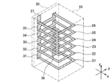
- FIG. 1 is a perspective view showing the appearance of the multilayer inductor according to the first embodiment of the present invention.
- FIG. 2 is a perspective view showing a conductor pattern of the multilayer inductor according to the first embodiment.
- FIG. 3 is an exploded perspective view of the multilayer inductor according to the first embodiment.
- FIG. 4 is a perspective view showing the appearance of the multilayer inductor according to the second embodiment of the present invention.
- FIG. 5 is a perspective view showing a conductor pattern of the multilayer inductor according to the second embodiment.
- FIG. 6 is an exploded perspective view of the multilayer inductor according to the second embodiment.
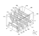
- FIG. 7 is a perspective view showing the internal structure of the multilayer inductor according to the third embodiment of the present invention in a transparent state.
- FIG. 1 is a perspective view showing the appearance of the multilayer inductor according to the first embodiment of the present invention.
- FIG. 2 is a perspective view showing a conductor pattern of the multilayer inductor according
- FIG. 8 is an exploded perspective view of the multilayer inductor according to the third embodiment.
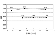
- FIG. 9 is a diagram showing a Q value of the multilayer inductor according to the third embodiment in comparison with a conventional multilayer inductor.
- FIG. 10 is an equivalent circuit diagram of the multilayer bandpass filter according to the fourth embodiment of the present invention.
- FIG. 11 is a perspective view showing the internal structure of the multilayer bandpass filter according to the fourth embodiment in a transparent state.
- FIG. 12 is an exploded perspective view of the multilayer bandpass filter according to the fourth embodiment.
- FIG. 13 is a diagram showing the frequency characteristics of the multilayer bandpass filter according to the fourth embodiment.
- FIG. 14 is a perspective view schematically showing one step of the manufacturing method suitable for manufacturing the multilayer electronic component according to the present invention.
- FIG. 15 is a perspective view schematically showing one step in the manufacturing method.
- FIG. 16 is a perspective view schematically showing one step in the manufacturing method.
- FIG. 17 is a perspective view schematically showing one step in the manufacturing method.
- FIG. 18 is a perspective view schematically showing one step in the manufacturing method.
- FIG. 19 is a perspective view schematically showing one step in the manufacturing method.
- FIG. 20 is a perspective view schematically showing one step in the manufacturing method.
- FIG. 21 is a perspective view schematically showing one step in the manufacturing method.
- FIG. 22 is a perspective view schematically showing one step in the manufacturing method.
- FIG. 23 is a perspective view schematically showing one step in the manufacturing method.
- FIG. 24 is a perspective view schematically showing one step in the manufacturing method.
- FIG. 25 is a diagram schematically showing a cross-section (cross-section BB in FIG. 24) of the reorganized laminated sheet in the manufacturing method.
- FIG. 26 is a perspective view schematically showing one step in the manufacturing method.
- FIG. 27 is a perspective view schematically showing one step in the manufacturing method.
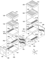
- FIG. 28 is a perspective view showing the internal structure of a conventional multilayer inductor in a transparent state.
- FIG. 29 is an exploded perspective view of the conventional multilayer inductor.
- the electronic component according to the first embodiment of the present invention includes ceramic sheets 11, 12, 13, and a plurality of internal wiring layers (six layers in the illustrated example). 14, 15, 16, and 17, and the second laminated body 30 having the wiring layer on the surface of the ceramic sheet, the lamination direction of the first laminated body 10 and the second laminated body 30 is They are joined so as to be orthogonal to each other (the wiring layer of the first laminated body 10 and the wiring layer of the second laminated body 30 form an angle of 90 ° with each other).
- inductor conductors 21, 22, 23, 24, 25, and 26 having a substantially U-shaped (substantially U-shaped) planar shape are formed.
- the inductor conductors 21 to 26 arranged in the wiring layer are arranged so as to overlap each other when viewed from the plane (when viewed from the z-axis direction in FIGS. 1 to 3). Further, both end portions (one end portions 21a to 26a and the other end portions 21b to 26b) of the inductor conductors 21 to 26 can be electrically connected to the connection conductors provided in the second laminate 30.
- the second laminated body 30 is exposed on the side surface of the first laminated body 10 to be joined.
- the internal wiring layers of the first laminate 10 are referred to as a first layer, a second layer,... From the bottom, and the uppermost internal wiring layer is referred to as a sixth layer.
- the inductor conductor 21 formed on the first layer is the first inductor conductor
- the inductor conductor 22 formed on the second layer is the second inductor conductor.
- the inductor conductor 21 is formed on the third to sixth layers.
- the inductor conductors 23 to 26 are referred to as a third inductor conductor, a fourth inductor conductor, a fifth inductor conductor, and a sixth inductor conductor, respectively (the same applies to the embodiments described later).
- the number of laminated layers is not particularly limited to this example (six layers or six), and may be smaller or larger.
- a plurality of the first to sixth inductor conductors 21 to 26 are electrically connected to the surface wiring layer of the second laminate 30 so that the inductor conductors 21 to 26 function as an inductor as a whole.
- Connection conductors 31, 32, 33, 34, and 35 are formed.
- the first connecting conductor 31 having 31b is formed on the surface of the second laminated body 30 to be a joint surface with the first laminated body 10, and the first inductor conductor 21 and the second inductor are formed by the first connecting conductor 31.
- the conductor 22 is electrically connected.
- the second connecting conductor 32 having the above is formed on the surface of the second laminated body 30, and the second connecting conductor 32 and the third inductor conductor 23 are electrically connected by the second connecting conductor 32.
- the third inductor conductor 23 to the sixth inductor conductor 26 are sequentially connected by the third connecting conductor 33, the fourth connecting conductor 34, and the fifth connecting conductor 35 that are provided in the same manner.
- the inductors are formed so that each of the inductor conductors 21 to 26 is spiral inside the first laminate 10.
- the first laminated body 10 may be provided with terminal electrodes (not shown) for external connection on the upper surface and the lower surface, respectively, or may be provided with other circuit elements by further laminating a ceramic sheet and providing a wiring layer.
- the connection conductors 36 and 37 are respectively provided at the upper end and the lower end of the surface of the second laminate 30 in the same manner as the connection conductor.
- the connection conductors 36 and 37 may be provided and connected to terminal electrodes and other circuit elements.
- the electronic component according to the second embodiment of the present invention includes a first laminate including an inductor conductor in each wiring layer of the ceramic laminate, and these inductor conductors.
- a pair of opposed first laminates 40 is provided.
- the second laminated body 80 and the third laminated body 90 are joined to the side surfaces of the two, respectively, and the inductor has a double spiral structure.
- each wiring layer of the first laminate 40 includes inductor conductors 61 to 70 having a substantially U-shaped (substantially U-shaped) planar shape as in the first embodiment.
- the inductor conductors 61 to 70 are laminated so that the orientations of the inductor conductors 61 to 70 are alternate every layer.
- the first inductor conductor 61 formed on the first layer, the third inductor conductor 63 formed on the third layer, the fifth inductor conductor 65 formed on the fifth layer, and the seventh layer are formed.
- the seventh inductor conductor 67 and the ninth inductor conductor 69 formed on the ninth layer are provided at both end portions thereof. Is rotated 180 degrees in the opposite direction (in the horizontal plane or in the xy plane) so as to be exposed on the side surface (second bonding surface) opposite to (opposed to) the side surface (first bonding surface). Arranged). And the 3rd laminated body 90 is joined to this opposing side surface (2nd joining surface).
- the first to tenth inductor conductors 61 to 70 are arranged so as to overlap each other when viewed from the plane except for the ends connected to the connection conductors 81 to 84 and 91 to 94, and the odd layer inductors.
- the inductor formed by the conductors 61, 63, 65, 67, 69 and the inductor formed by the even-layer inductor conductors 62, 64, 66, 68, 70 form a double helix to form one inductor as a whole.
- the second laminated body 80 and the third laminated body 90 are provided with connection conductors 81 to 84 and 91 to 94 similar to those of the first embodiment on their surfaces (bonding surfaces with the first laminated body 40).
- the inductor conductors 61 to 70 of the first laminated body 40 are connected to form a spiral inductor.
- the joint surface of the second stacked body 80 and the third stacked body 90 is the opposite side surface of the first stacked body 40, but the double spiral structure inductor is similarly configured as the adjacent side surface.
- the double spiral structure inductor is similarly configured as the adjacent side surface.
- the odd layer inductor conductors 61, 63, 65, 67, 69 and the even layer inductor conductors 62, 64, 66, 68, 70 are arranged so as to form an angle of 90 ° with each other when viewed from the plane. good.
- an inductor having a triple or quadruple helical structure can be similarly configured.
- the electronic component according to the third embodiment of the present invention includes inductor conductors 111, 112, and the like for each wiring layer of the ceramic laminate as in the first and second embodiments.
- the first laminated body 100 provided with 113, 114, 115, 116, 117 and the laminated body (first article) provided with connecting conductors 121, 122, 123, 131, 132, 133 connecting these inductor conductors 111 to 117.
- each of the inductor conductors 111 to 117 extends between a pair of opposing side surfaces of the first laminated body 100.
- the first laminated body 100 is formed by laminating ceramic sheets 101 to 109 in the front-rear direction (y-axis direction), and the second laminated body 100 has a second surface on one side surface (first bonding surface).
- the laminated body 120 is joined so that the wiring layer of the first laminated body 100 and the wiring layer of the second laminated body 120 are orthogonal to each other, and on the other side surface (second bonded surface) of the first laminated body 100.
- the third stacked body 130 is joined so that the wiring layer of the first stacked body 100 and the wiring layer of the third stacked body 130 are orthogonal to each other.
- strip-shaped inductor electrodes (first electrodes, one end of which is exposed to the first joint surface and the other end of the second multilayer are exposed to the second joint surface).
- 1 to 7 inductor conductors) 111 to 117 are formed.
- the inductor conductor formed in the odd layer that is, the first inductor conductor 111 formed in the first layer
- the third inductor conductor 113 formed in the third layer the fifth inductor conductor 115 formed on the fifth layer and the seventh inductor conductor 117 formed on the seventh layer extend horizontally below the respective wiring layers close to the bottom surface of the first multilayer body 100.
- the inductor conductor formed in the even layer that is, the second inductor conductor 112 formed in the second layer, the fourth inductor conductor 114 formed in the fourth layer, and the sixth inductor formed in the sixth layer.
- the conductors 116 are formed so as to extend horizontally on top of each wiring layer near the top surface of the first laminate 100.
- the odd-numbered inductor conductors first inductor conductor 111, third inductor conductor 113, and fifth inductor conductor 115.
- the seventh inductor conductor 117 overlap each other, and the even-number inductor conductors (second inductor conductor 112, fourth inductor conductor 114, and sixth inductor conductor 116) overlap each other.
- the odd-numbered inductor conductors 111, 113, 115, 117 and the even-numbered inductor conductors 112, 114, 116 extend in parallel and horizontally with a certain distance from each other. It is arranged in.
- one end 112a of the second inductor conductor 112 and one end 113a of the third inductor conductor 113 are connected by a connection conductor 121 provided on the surface of the second laminate 120, and The one end portion 114a of the fourth inductor conductor 114 and the one end portion 115a of the fifth inductor conductor 115 are connected by the connection conductor 122 provided on the surface of the second laminate 120, and the one end portion 116a of the sixth inductor conductor 116 is connected.
- One end portion 117 a of the seventh inductor conductor 117 is connected by a connection conductor 123 provided on the surface of the second multilayer body 120.
- the other end 111b of the first inductor conductor 111 and the other end 112b of the second inductor conductor 112 are connected to each other at the second joint surface by a connection conductor 131 provided on the surface of the third multilayer body 130.
- the other end 113b of the third inductor conductor 113 and the other end 114b of the fourth inductor conductor 114 are connected by the connection conductor 132 provided on the surface of the third laminated body 130, and the fifth inductor conductor 115 is connected.
- the other end portion 115b of the sixth inductor conductor 116 and the other end portion 116b of the sixth inductor conductor 116 are connected by a connection conductor 133 provided on the surface of the third laminated body 130.
- the first inductor conductor to the seventh inductor conductor are electrically connected in order, and a spiral inductor extending in the stacking direction (front-rear direction / y-axis direction) is formed inside the first stacked body. I can do it.
- terminal electrodes for external connection can be provided on the front surface and the rear surface of the first laminated body 100, and the terminal electrodes on the front surface side and the one end 111a of the first inductor conductor 111 are connected to each other.
- a through hole V is formed in order to connect, and a through hole V is formed in order to connect the terminal electrode on the rear surface side and the other end 117b of the seventh inductor conductor 117.
- connection conductors provided on the surface of the second laminate 120 and the surface of the third laminate 130, respectively.
- FIG. 9 shows a comparison between the Q value of the inductor of the present embodiment and the Q value of the conventional inductor shown in FIGS. 28 to 29, in which the solid line is the present embodiment, and the alternate long and short dash line is the conventional one. Structure. As is apparent from this figure, according to the present embodiment, it is possible to obtain a higher Q value than the conventional structure in which an inductor is formed using a through hole.
- the electronic component according to the fourth embodiment of the present invention has two stages of resonators, that is, an LC resonator 143 composed of an inductor L1 and a capacitor C1, and an LC resonance composed of an inductor L2 and a capacitor C2.
- This is a band-pass filter in which a pass band is formed by providing a device 144 between the input / output terminals 141 and 142.
- the laminated structure includes a first laminated body 150 including a first-stage resonator (first-stage resonator) 143 and a second-stage resonator (second-stage resonator).
- (Resonator) 144 having a built-in 144 and a third laminate 160 joined to the rear surface of the first laminate 150 and the front surface of the second laminate 160 so as to be interposed between the laminates 150 and 160.
- the wiring layer of the first stacked body 150 and the wiring layer of the second stacked body 160 are parallel to each other, and the wiring layers of the third stacked body 170, the fourth stacked body 180, and the fifth stacked body 190 are parallel to each other. It is.
- the wiring layers of the first stacked body 150 and the second stacked body 160 and the wiring layers of the third stacked body 170, the fourth stacked body 180, and the fifth stacked body 190 are orthogonal to each other.
- the first laminated body 150 and the second laminated body 160 have five ceramic sheets 151, 152, 153, 154, 155 so as to have four internal wiring layers. 161, 162, 163, 164, and 165 are laminated ceramic layers in the vertical direction (z-axis direction), respectively, and the fourth laminated body 180 and the fifth laminated body 190 are the second laminated layers of the third embodiment. Similar to the body 120 and the third laminate 130, the connection conductors are provided on the surface, and the third laminate 170 is provided with the connection conductors 171, 172;
- the first to third layers of the first laminate are provided with inductor conductors 201, 202, and 203, and the fourth layer is provided with a capacitor electrode 220.
- the second laminate 160 includes inductor conductors 211, 212, 213 and a capacitor electrode 220.
- These inductor conductors 201 to 203 and 211 to 213 are strip-like electrodes as in the third embodiment, and are arranged at one end 201a on the front surface of the first laminate 150, which is a joint surface with the fourth laminate 180.
- first laminate 150 which is a joint surface with the third laminate 170, and are linear in the front-rear direction (y-axis direction). (The same applies to the second laminate 160).
- first-layer first inductor conductor 201 and third-layer third inductor conductor 203 overlap each other when viewed from above, and even-layer inductor conductors (second-layer first conductors 201).
- the two-inductor conductor 202) is arranged in parallel with the odd-numbered inductor conductors 201 and 203 with a certain distance therebetween.
- the first inductor conductor 201, the second inductor conductor 202, and the third inductor conductor 203 are connected to conductors 171 and 172 provided on the front surface (front surface) of the third laminate 170, and the fourth laminate 180.
- the inductor conductor and the capacitor electrode can be connected in the same manner as the inductor conductors. That is, the connection between the third inductor conductor 203 of the first laminate 150 and the capacitor electrode 220 is made by the connection conductor 172 provided on the surface (front surface) of the third laminate 170 for the third inductor of the second laminate 160. The connection between the conductor 213 and the capacitor electrode 220 may be performed by a connection conductor 174 provided on the back surface (rear surface) of the third laminate 170.
- the capacitor electrodes 220 constitute capacitors C 1 and C 2 of the resonators 143 and 144 by facing the ground electrodes 221 formed on the top surfaces of the first stacked body 150 and the second stacked body 160.
- an input terminal electrode (not shown) is provided at the front end portion of the bottom surface of the first laminated body 150, and the input terminal electrode and one end portion 201 a of the first inductor conductor 201 are connected via the through hole V. Connecting. Further, an output terminal electrode (not shown) is provided at the rear end portion of the bottom surface of the second multilayer body 160, and the output terminal electrode and the other end portion 211b of the first inductor conductor 211 through the through hole V. And connect. A ground electrode (not shown) is formed between the input terminal electrode and the output terminal electrode over the bottom surfaces of the first stacked body 150, the third stacked body 170, and the second stacked body 160.
- the ground electrode and the ground electrode 221 formed on the top surfaces of the first laminate 150 and the second laminate 160 are formed on the side surfaces of the first laminate 150, the third laminate 170, and the second laminate 160. It is possible to connect by a surface electrode formed so as to spread.
- FIG. 13 shows the frequency characteristics of the bandpass filter of the present embodiment, where the solid line indicates the pass characteristic and the broken line indicates the cutoff characteristic.
- the bandpass filter of this embodiment it is possible to realize a pass characteristic of approximately 1.0 dB in the 5 GHz band, which is one of the wireless LAN standards that enables high-speed transmission.
- the method of manufacturing the electronic component according to the present invention is not limited to this, but the previous proposal by the applicant (Japanese Patent Application No. 2010-165398) can be preferably applied.
- this method will be briefly described with reference to FIGS. 14 to 27 by taking the bandpass filter of the fourth embodiment as an example.
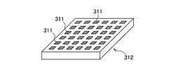
- (1) Production of Laminated Sheet / Laminated Stick As shown in FIG. 14, first, an unfired green sheet formed of a ceramic material is prepared, and a conductive paste is applied to the surface of the first laminated bodies 150 and 160. Ceramic sheets 301, 302, 303, 304, and 305 are produced by printing a predetermined conductor pattern corresponding to each wiring layer. The conductor patterns 311 printed on each of the ceramic sheets 301 to 305 are formed so as to be arranged in a matrix in the vertical and horizontal directions corresponding to the number of chips to be manufactured. Each conductor pattern 311 shown in FIG. 14 (the same applies to FIGS. 15 to 27) is intended to illustrate the concept of the manufacturing method, and is intended to accurately represent the conductor shape of the embodiment. Not what you want.
- the ceramic sheets 301 to 305 are superposed in a predetermined order while being aligned, and these are laminated by thermocompression bonding to obtain a first laminated sheet 312 as shown in FIG.
- the said 1st lamination sheet 312 is cut
- a plurality of conductor pattern sets constituting the first laminated body 150 are arranged in a laminated state.
- the second laminated body 160 is also subjected to the same process, and the second laminated stick 323 in which a plurality of sets of conductor patterns constituting the second laminated body 160 are arranged in the length direction is produced.
- the third laminated stick is produced.
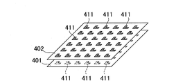
- an unfired green sheet is prepared in the same manner as in the production of the first laminated sheet, and a predetermined paste corresponding to the front and back surfaces of the third laminated body 170 is applied by applying a conductive paste to the surface.
- Ceramic sheets 401 and 402 on which the conductor pattern is printed are prepared.
- the conductor patterns formed on each of the ceramic sheets 401 and 402 are arranged in a matrix in the vertical direction and the horizontal direction, respectively, as in the first laminated sheet.
- the ceramic sheets 401 and 402 are overlapped while being aligned, and these are integrated by thermocompression bonding, thereby producing a third laminated sheet 412 as shown in FIG.
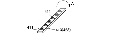
- the 3rd lamination sheet 412 is cut
- a plurality of sets of conductor patterns 181 and 191 constituting the fourth laminate 180 and the fifth laminate 190 are arranged in the longitudinal direction.
- a fourth laminated stick 423 is produced.
- the conductive pattern (connecting conductor 181) of the fourth laminated body 180 is formed on one surface of the front and back surfaces, and the conductive pattern (connecting conductor 191) of the fifth laminated body 190 is formed on the other surface. It shall be assumed.
- a ceramic sheet is further interposed between the ceramic sheet on one side where the conductor pattern of the fourth laminate 180 is formed and the ceramic sheet on the other side where the conductor pattern of the fifth laminate 190 is formed. What is necessary is just to laminate.
- the third laminated stick 413 and the fourth laminated stick 423 are arranged so that their wiring layers (front and back surfaces) stand vertically. Rotate 90 ° around the longitudinal direction.
- the first laminated stick 313 and the second laminated stick 323 are alternately arranged and rotated by 90 ° between the first laminated stick 313 and the second laminated stick 323.
- the first to fourth laminated sticks 313, 323, 413, 423 are integrated by thermocompression bonding as shown in FIG. .
- the reorganization lamination sheet 512 shown in FIG. 24 is obtained.
- the reorganized laminated sheet 512 includes a fourth laminated stick 423 (fourth laminated body 180), a first laminated stick 313 (first laminated body 150), and a third laminated stick 413 (first laminated).
- a fourth laminated stick 423 fourth laminated body 180
- a first laminated stick 313 first laminated body 150
- a third laminated stick 413 first laminated.
- Three laminated bodies 170), a second laminated stick 323 (second laminated body 160), and a fourth laminated stick 423 (fifth laminated body 190) are joined, and the conductors included in each adjacent laminated stick are connected to each other. Electrically connected.
- the third laminated sheet 512 is cut in a grid shape (diced shape) in the vertical direction and the horizontal direction at a cutting line 510 (see also FIG. 25), and is shown in FIG. 27.
- the chip 522 is obtained.
- the individual chips 522 are fired.
- the ceramic layers of the first to fifth laminates 150, 160, 170, 180, and 190 are sintered to form one continuous sintered body.
- external electrodes terminal electrodes
- the filter chip of the fourth embodiment can be manufactured.
- the electronic component according to the present invention can be manufactured with high productivity.
- the said manufacturing method is applicable similarly about the electronic component which concerns on other embodiment.
- C1, C2 capacitors L1, L2 inductors V through holes 1a, 1b, 1c, 1d, 1e, 1f, 1g, 1h, 11, 12, 13, 14, 15, 16, 17, 101, 102, 103, 104, 105 , 106, 107, 108, 109, 151, 152, 153, 154, 155, 161, 162, 163, 164, 165, 301, 302, 303, 304, 305, 401, 402 Ceramic green sheets 2a, 2b, 2c , 2d, 2e, 2f, 2g, 21, 22, 23, 24, 25, 26, 61, 62, 63, 64, 65, 66, 67, 68, 69, 70, 111, 112, 113, 114, 115 , 116, 117, 201, 202, 203, 211, 212, 213 Inductor conductor 10, 40, 100, 150 First laminated 21a, 22a, 23a, 24a, 25a, 26a, 61a, 62
Landscapes
- Engineering & Computer Science (AREA)
- Power Engineering (AREA)
- Microelectronics & Electronic Packaging (AREA)
- Coils Or Transformers For Communication (AREA)
Abstract
Description
特許文献2:特開2009-170737号公報
本発明の第一の実施形態に係る電子部品は、図1から図3に示すように、複数(図示の例の場合6層)の内部配線層を備えるようにセラミックシート11,12,13,14,15,16,17を積層した第一積層体10と、セラミックシートの表面に配線層を備えた第二積層体30とを、第一積層体10と第二積層体30の積層方向が互いに直交するように(第一積層体10の配線層と第二積層体30の配線層とが互いに90°の角度をなすように)接合したものである。
本発明の第二の実施形態に係る電子部品は、前記第一実施形態のインダクタと同様に、セラミック積層体の各配線層にインダクタ用導体を備えた第一積層体と、これらのインダクタ用導体をインダクタを形成するように接続する接続導体を備えた積層体とを有するものであるが、前記第一実施形態と異なり、図4から図6に示すように第一積層体40の対向する一対の側面にそれぞれ第二積層体80と第三積層体90を接合し、インダクタが二重螺旋構造を有する。
本発明の第三の実施形態に係る電子部品は、図7から図8に示すように、前記第一および第二実施形態と同様にセラミック積層体の各配線層にインダクタ用導体111,112,113,114,115,116,117を備えた第一積層体100と、これらのインダクタ用導体111~117を接続する接続導体121,122,123,131,132,133を備えた積層体(第二積層体120および第三積層体130)とを有するものであるが、前記実施形態と異なり、各インダクタ用導体111~117が第一積層体100の対向する一対の側面の間に亘って延びる直線状の電極であり、これらの電極を、インダクタを形成するように第二積層体120に設けた接続導体121~123と第三積層体130に設けた接続導体131~133とで接続する。
本発明の第四の実施形態に係る電子部品は、図10に示すように共振器を2段、すなわち、インダクタL1とキャパシタC1からなるLC共振器143と、インダクタL2とキャパシタC2からなるLC共振器144とを入出力端子141,142間に備えることにより通過帯域を形成したバンドパスフィルタである。
本発明に係る電子部品を製造する方法としては、これに限定されるわけではないが、本出願人による先の提案(特願2010-165398)を好ましく適用することが出来る。以下、この方法について図14から図27を参照し、前記第四実施形態のバンドパスフィルタを例にとって簡潔に説明する。
図14に示すようにまず、セラミック材料により形成した未焼成のグリーンシートを用意し、その表面に導電性ペーストを塗布して第一積層体150,160の各配線層に対応した所定の導体パターンを印刷することによりセラミックシート301,302,303,304,305を作製する。これらセラミックシート301~305の各々に印刷する導体パターン311は、作製するチップの数に対応した数だけ縦方向と横方向とにマトリックス状に配列するように形成する。なお、図14(図15から図27についても同様)に示した各導体パターン311は、当該製造方法の概念を示すためのものであって、前記実施形態の導体形状を正確に表すことを意図するものではない。
図20から図21に示すように第三積層スティック413および第四積層スティック423を、それらの配線層(表裏面)が垂直に立つように当該積層スティック413,423の長手方向の周りに90°回転させる。
図26に示すように切断線510(図25も参照)において第三積層シート512を縦方向と横方向とに方眼状(さいの目状)に切断し、図27に示すようにチップ522を得る。その後、個々のチップ522を焼成する。これにより、第一から第五の各積層体150,160,170,180,190のセラミック層が焼結して連続したひとつの焼結体となる。なお、焼成後には、チップ522の外表面に外部電極(端子電極)を適宜形成すれば良い。
L1,L2 インダクタ
V スルーホール
1a,1b,1c,1d,1e,1f,1g,1h,11,12,13,14,15,16,17,101,102,103,104,105,106,107,108,109,151,152,153,154,155,161,162,163,164,165,301,302,303,304,305,401,402 セラミックグリーンシート
2a,2b,2c,2d,2e,2f,2g,21,22,23,24,25,26,61,62,63,64,65,66,67,68,69,70,111,112,113,114,115,116,117,201,202,203,211,212,213 インダクタ用導体
10,40,100,150 第一積層体
21a,22a,23a,24a,25a,26a,61a,62a,63a,64a,65a,66a,67a,68a,69a,70a,111a,112a,113a,114a,115a,116a,117a,201a,202a,203a,211a,212a,213a インダクタ用導体の一端部
21b,22b,23b,24b,25b,26b,61b,62b,63b,64b,65b,66b,67b,68b,69b,70b,111b,112b,113b,114b,115b,116b,117b,201b,202b,203b,211b,212b,213b インダクタ用導体の他端部
30,80,120,160 第二積層体
31,32,33,34,35,36,37,81,82,83,84,91,92,93,94,121,122,123,131,132,133,171,172,173,174,181,191 接続導体
31a,32a,33a,34a,35a,81a,82a,83a,84a,91a,92a,93a,94a 接続導体の一端部
31b,32b,33b,34b,35b,81b,82b,83b,84b,91b,92b,93b,94b 接続導体の他端部
90,130,170 第三積層体
141 入力端子
142 出力端子
143 第1段LC共振器
144 第2段LC共振器
180 第四積層体
190 第五積層体
220 キャパシタ電極
221 グランド電極
311,411 導体パターン
312 第一積層シート
313 第一積層スティック
323 第二積層スティック
412 第三積層シート
413 第三積層スティック
423 第四積層スティック
510 切断線
512 再編積層シート
522 フィルタチップ
Claims (5)
- 絶縁層を介して積層した2層以上の配線層を有する第一積層体と、
少なくとも1層の絶縁層とその表面に形成した配線層とを備えかつ前記第一積層体に接合した第二積層体と
を含む積層型電子部品であって、
前記第一積層体の配線層と、前記第二積層体の配線層とは互いに略直交し、
前記第一積層体は、
前記2層以上の配線層のうちの第一の配線層に配した第一インダクタ用導体と、
前記2層以上の配線層のうちの第二の配線層に配した第二インダクタ用導体と、
を有し、
前記第二積層体は、
前記第一インダクタ用導体および前記第二インダクタ用導体がコイル状のインダクタを形成するように前記第一積層体との接合面において前記第一インダクタ用導体の端部と前記第二インダクタ用導体の端部とを電気的に接続する接続導体
を有する
ことを特徴とするコイル状のインダクタを含む積層型電子部品。 - 前記第一積層体は、直方体の全体形状を有し、
前記第一インダクタ用導体は、前記第一の配線層においてループ状に形成されて一端部および他端部が前記第二積層体との接合面にそれぞれ露出し、
前記第二インダクタ用導体は、前記第二の配線層において前記第一インダクタ用導体と略重なるようにループ状に形成されて、一端部が前記第二積層体との接合面に露出するとともに前記第一積層体の積層方向に関し前記第一インダクタ用導体の一端部と略重なる位置に配置され、かつ、他端部が前記第二積層体との接合面に露出するとともに前記第一積層体の積層方向に関し前記第一インダクタ用導体の他端部と略重なる位置に配置され、
前記接続導体は、前記第一インダクタ用導体の他端部と、前記第二インダクタ用導体の一端部とを電気的に接続する
請求項1に記載の積層型電子部品。 - 絶縁層を介して積層した4層以上の配線層を有しかつ直方体の全体形状を有する第一積層体と、
少なくとも1層の絶縁層とその表面に形成した配線層とを備えかつ前記第一積層体に接合した第二積層体と、
少なくとも1層の絶縁層とその表面に形成した配線層とを備えかつ前記第一積層体に接合した第三積層体と
を備えた積層型電子部品であって、
前記第二積層体の配線層および前記第三積層体の配線層はともに、前記第一積層体の配線層と略直交し、
前記第一積層体の表面のうち、前記第二積層体が接合される面を第一接合面としたときに、前記第三積層体は、当該第一接合面に対向又は隣接する第一積層体の表面である第二接合面に接合され、
前記第一積層体に含まれる4層の配線層をより上層に位置する配線層から順に、第一配線層、第二配線層、第三配線層、および第四配線層としたときに、前記第一積層体は、
第一配線層に配した第一インダクタ用導体と、
第二配線層に配した第二インダクタ用導体と、
第三配線層に配した第三インダクタ用導体と、
第四配線層に配した第四インダクタ用導体と、
を有し、
前記第一インダクタ用導体は、前記第一の配線層においてループ状に形成されて一端部および他端部が前記第一接合面にそれぞれ露出し、
前記第二インダクタ用導体は、前記第二の配線層において前記第一インダクタ用導体と略重なるようにループ状に形成されて一端部および他端部が前記第二接合面にそれぞれ露出し、
前記第三インダクタ用導体は、前記第三の配線層において前記第一インダクタ用導体および前記第二インダクタ用導体と略重なるようにループ状に形成されて、一端部が前記第一接合面に露出するとともに前記第一積層体の積層方向に関し前記第一インダクタ用導体の一端部と略重なる位置に配置され、かつ、他端部が前記第一接合面に露出するとともに前記第一積層体の積層方向に関し前記第一インダクタ用導体の他端部と略重なる位置に配置され、
前記第四インダクタ用導体は、前記第四の配線層において前記第一インダクタ用導体、前記第二インダクタ用導体および前記第三インダクタ用導体と略重なるようにループ状に形成されて、一端部が前記第二接合面に露出するとともに前記第一積層体の積層方向に関し前記第二インダクタ用導体の一端部と略重なる位置に配置され、かつ、他端部が前記第二接合面に露出するとともに前記第一積層体の積層方向に関し前記第二インダクタ用導体の他端部と略重なる位置に配置され、
前記第二積層体は、前記第一インダクタ用導体および前記第三インダクタ用導体がコイル状のインダクタを形成するように前記第一接合面において当該第一インダクタ用導体の他端部と当該第三インダクタ用導体の一端部とを電気的に接続する第一接続導体を有し、
前記第三積層体は、前記第二インダクタ用導体および前記第四インダクタ用導体がコイル状のインダクタを形成するように前記第二接合面において当該第二インダクタ用導体の他端部と当該第四インダクタ用導体の一端部とを電気的に接続する第二接続導体を有する
ことを特徴とするコイル状のインダクタを含む積層型電子部品。 - 絶縁層を介して積層した3層以上の配線層を有しかつ直方体の全体形状を有する第一積層体と、
少なくとも1層の絶縁層とその表面に形成した配線層を備えかつ前記第一積層体に接合した第二積層体と、
少なくとも1層の絶縁層とその表面に形成した配線層を備えかつ前記第一積層体に接合した第三積層体と
を備えた積層型電子部品であって、
前記第二積層体の配線層および前記第三積層体の配線層はともに、前記第一積層体の配線層と略直交し、
前記第一積層体の表面のうち、前記第二積層体が接合される面を第一接合面としたときに、前記第三積層体は、当該第一接合面に対向する第一積層体の表面である第二接合面に接合され、
前記第一積層体に含まれる3層の配線層をより上層に位置する配線層から順に、第一配線層、第二配線層、および第三配線層としたときに、前記第一積層体は、
一端部が前記第一接合面に露出するとともに他端部が前記第二接合面に露出しかつ前記第一接合面から前記第二接合面まで延在するように前記第一配線層に形成した第一インダクタ用導体と、
一端部が前記第一接合面に露出するとともに他端部が前記第二接合面に露出しかつ前記第一接合面から前記第二接合面まで延在するように前記第二配線層に形成した第二インダクタ用導体と、
一端部が前記第一接合面に露出するとともに他端部が前記第二接合面に露出しかつ前記第一接合面から前記第二接合面まで延在するように前記第三配線層に形成した第三インダクタ用導体と、
を有し、
前記第一インダクタ用導体と前記第三インダクタ用導体とは、前記第一積層体の積層方向から見たときに略重なるように配置される一方、
前記第一インダクタ用導体および前記第三インダクタ用導体と、前記第二インダクタ用導体とは、前記第一積層体の積層方向から見たときに互いに間隔を隔てて配置され、
前記第二積層体は、
前記第一インダクタ用導体および前記第二インダクタ用導体がコイル状のインダクタを形成するように前記第一接合面において前記第一インダクタ用導体の一端部と前記第二インダクタ用導体の一端部とを電気的に接続する第一接続導体
を有し、
前記第三積層体は、
前記第二インダクタ用導体および前記第三インダクタ用導体がコイル状のインダクタを形成するように前記第二接合面において前記第二インダクタ用導体の他端部と前記第三インダクタ用導体の他端部とを電気的に接続する第二接続導体
を有する
ことを特徴とするコイル状のインダクタを含む積層型電子部品。 - 絶縁層を介して積層した2層以上の配線層を有しかつ直方体の全体形状を有する第一積層体と、
絶縁層を介して積層した2層以上の配線層を有しかつ直方体の全体形状を有する第二積層体と、
表面に形成した表面配線層と裏面に形成した裏面配線層とを有して前記第一積層体と前記第二積層体との間に介在され、前記表面配線層が前記第一積層体に当接するとともに前記裏面配線層が前記第二積層体に当接するように前記第一積層体と前記第二積層体とに接合された第三積層体と
を備え、
前記第三積層体の表面配線層は、前記第一積層体の配線層と略直交し、
前記第三積層体の裏面配線層は、前記第二積層体の配線層と略直交する
積層型電子部品であって、
前記第一積層体は、
当該第一積層体の前記2層以上の配線層のうちの第一の配線層に配した第一インダクタ用導体と、
当該第一積層体の前記2層以上の配線層のうちの第二の配線層に配した第二インダクタ用導体と、
を有し、
前記第二積層体は、
当該第二積層体の前記2層以上の配線層のうちの第一の配線層に配した第三インダクタ用導体と、
当該第二積層体の前記2層以上の配線層のうちの第二の配線層に配した第四インダクタ用導体と、
を有し、
前記第三積層体は、
前記第一インダクタ用導体と前記第二インダクタ用導体とがコイル状のインダクタを形成するように前記第一積層体との接合面において前記第一インダクタ用導体の端部と前記第二インダクタ用導体の端部とを電気的に接続する第一接続導体を前記表面配線層に有するとともに、
前記第三インダクタ用導体と前記第四インダクタ用導体とがコイル状のインダクタを形成するように前記第二積層体との接合面において前記第三インダクタ用導体の端部と前記第四インダクタ用導体の端部とを電気的に接続する第二接続導体を前記裏面配線層に有する
ことを特徴とするコイル状のインダクタを含む積層型電子部品。
Priority Applications (2)
| Application Number | Priority Date | Filing Date | Title |
|---|---|---|---|
| CN201180034187.1A CN102985983B (zh) | 2010-09-09 | 2011-09-07 | 包含电感器的层叠型电子部件 |
| US13/580,021 US20120313743A1 (en) | 2010-09-09 | 2011-09-07 | Laminated electronic component equipped with inductor |
Applications Claiming Priority (2)
| Application Number | Priority Date | Filing Date | Title |
|---|---|---|---|
| JP2010-201959 | 2010-09-09 | ||
| JP2010201959A JP5692502B2 (ja) | 2010-09-09 | 2010-09-09 | インダクタを含む積層型電子部品 |
Publications (1)
| Publication Number | Publication Date |
|---|---|
| WO2012033136A1 true WO2012033136A1 (ja) | 2012-03-15 |
Family
ID=45810733
Family Applications (1)
| Application Number | Title | Priority Date | Filing Date |
|---|---|---|---|
| PCT/JP2011/070399 Ceased WO2012033136A1 (ja) | 2010-09-09 | 2011-09-07 | インダクタを含む積層型電子部品 |
Country Status (4)
| Country | Link |
|---|---|
| US (1) | US20120313743A1 (ja) |
| JP (1) | JP5692502B2 (ja) |
| CN (1) | CN102985983B (ja) |
| WO (1) | WO2012033136A1 (ja) |
Cited By (1)
| Publication number | Priority date | Publication date | Assignee | Title |
|---|---|---|---|---|
| WO2022195869A1 (ja) * | 2021-03-19 | 2022-09-22 | 日本たばこ産業株式会社 | 吸引装置、電磁誘導源、電磁誘導源の製造方法、及びシステム |
Families Citing this family (12)
| Publication number | Priority date | Publication date | Assignee | Title |
|---|---|---|---|---|
| JP5704114B2 (ja) | 2012-05-07 | 2015-04-22 | 株式会社村田製作所 | 高周波モジュール |
| JP2013243366A (ja) * | 2012-05-22 | 2013-12-05 | Samsung Electro-Mechanics Co Ltd | チップインダクタおよびその製造方法 |
| JP6031854B2 (ja) * | 2012-07-04 | 2016-11-24 | Tdk株式会社 | コモンモードフィルタ |
| JP2015018862A (ja) * | 2013-07-09 | 2015-01-29 | 富士通株式会社 | 2重螺旋構造電子部品、2重螺旋構造電子部品の製造方法及び多機能シート |
| WO2016094140A1 (en) * | 2014-12-10 | 2016-06-16 | Suzhou Qing Xin Fang Electronics Technology Co., Ltd. | Methods and devices of laminated integrations of semiconductor chips, magnetics, and capacitance |
| KR102414839B1 (ko) * | 2016-01-29 | 2022-06-30 | 삼성전기주식회사 | 코일 부품 |
| JP7032214B2 (ja) | 2018-04-02 | 2022-03-08 | 株式会社村田製作所 | 積層型コイル部品 |
| JP6954217B2 (ja) * | 2018-04-02 | 2021-10-27 | 株式会社村田製作所 | 積層型コイル部品 |
| JP7020455B2 (ja) * | 2019-05-24 | 2022-02-16 | 株式会社村田製作所 | 積層型コイル部品 |
| JP7127610B2 (ja) * | 2019-05-24 | 2022-08-30 | 株式会社村田製作所 | 積層型コイル部品 |
| KR102748946B1 (ko) * | 2019-08-08 | 2025-01-02 | 삼성전기주식회사 | 적층 세라믹 커패시터 |
| JP7243696B2 (ja) * | 2020-09-09 | 2023-03-22 | 株式会社村田製作所 | 積層型コイル部品 |
Citations (3)
| Publication number | Priority date | Publication date | Assignee | Title |
|---|---|---|---|---|
| JPH06236817A (ja) * | 1993-02-12 | 1994-08-23 | Hitachi Zosen Corp | ノイズフィルターの製造方法 |
| JP2008066671A (ja) * | 2006-09-11 | 2008-03-21 | Fuji Electric Device Technology Co Ltd | 薄型磁気部品及びその製造方法 |
| JP2008066592A (ja) * | 2006-09-08 | 2008-03-21 | Fuji Electric Holdings Co Ltd | 薄型磁気部品の製造方法 |
Family Cites Families (6)
| Publication number | Priority date | Publication date | Assignee | Title |
|---|---|---|---|---|
| JP3438859B2 (ja) * | 1996-11-21 | 2003-08-18 | ティーディーケイ株式会社 | 積層型電子部品とその製造方法 |
| JP3201309B2 (ja) * | 1997-05-23 | 2001-08-20 | 株式会社村田製作所 | 積層型コイル及びその製造方法 |
| US6911889B2 (en) * | 2001-08-20 | 2005-06-28 | Steward, Inc. | High frequency filter device and related methods |
| JP4010919B2 (ja) * | 2002-09-30 | 2007-11-21 | Tdk株式会社 | インダクティブ素子の製造方法 |
| JP4010920B2 (ja) * | 2002-09-30 | 2007-11-21 | Tdk株式会社 | インダクティブ素子の製造方法 |
| CN1661736A (zh) * | 2004-02-27 | 2005-08-31 | Tdk株式会社 | 感应元件及其制造方法 |
-
2010
- 2010-09-09 JP JP2010201959A patent/JP5692502B2/ja active Active
-
2011
- 2011-09-07 CN CN201180034187.1A patent/CN102985983B/zh active Active
- 2011-09-07 WO PCT/JP2011/070399 patent/WO2012033136A1/ja not_active Ceased
- 2011-09-07 US US13/580,021 patent/US20120313743A1/en not_active Abandoned
Patent Citations (3)
| Publication number | Priority date | Publication date | Assignee | Title |
|---|---|---|---|---|
| JPH06236817A (ja) * | 1993-02-12 | 1994-08-23 | Hitachi Zosen Corp | ノイズフィルターの製造方法 |
| JP2008066592A (ja) * | 2006-09-08 | 2008-03-21 | Fuji Electric Holdings Co Ltd | 薄型磁気部品の製造方法 |
| JP2008066671A (ja) * | 2006-09-11 | 2008-03-21 | Fuji Electric Device Technology Co Ltd | 薄型磁気部品及びその製造方法 |
Cited By (1)
| Publication number | Priority date | Publication date | Assignee | Title |
|---|---|---|---|---|
| WO2022195869A1 (ja) * | 2021-03-19 | 2022-09-22 | 日本たばこ産業株式会社 | 吸引装置、電磁誘導源、電磁誘導源の製造方法、及びシステム |
Also Published As
| Publication number | Publication date |
|---|---|
| CN102985983A (zh) | 2013-03-20 |
| JP5692502B2 (ja) | 2015-04-01 |
| CN102985983B (zh) | 2015-03-25 |
| JP2012059937A (ja) | 2012-03-22 |
| US20120313743A1 (en) | 2012-12-13 |
Similar Documents
| Publication | Publication Date | Title |
|---|---|---|
| JP5692502B2 (ja) | インダクタを含む積層型電子部品 | |
| TWI442624B (zh) | Laminated bandpass filter | |
| JP5305042B2 (ja) | 積層型電子部品の製造方法 | |
| CN101946364A (zh) | 层叠带通滤波器 | |
| JP2009194096A (ja) | 部品内蔵基板、及びそれを用いた部品パッケージ | |
| JP5861693B2 (ja) | 積層バンドパスフィルタ | |
| CN104756403B (zh) | Lc滤波器单元体以及lc滤波器 | |
| TWI260659B (en) | LC composite component | |
| JP6380717B2 (ja) | Lcフィルタおよびlcフィルタの製造方法 | |
| US6922129B2 (en) | High-work-efficiency multilayered circuit board | |
| EP1150375B1 (en) | LC-included electronic component | |
| JP2002271038A (ja) | 複合多層基板およびその製造方法ならびに電子部品 | |
| TWI712261B (zh) | 積層平衡-不平衡轉換器 | |
| WO1994022281A1 (fr) | Carte de circuit imprime feuilletee | |
| JP3368817B2 (ja) | 積層型電子部品アレイ | |
| JP2000269078A (ja) | 積層電子部品 | |
| WO2014156719A1 (ja) | バンドパスフィルタ | |
| JPH03263311A (ja) | 積層複合部品 | |
| JP2008053543A (ja) | 積層チップ部品 | |
| JP2006041632A (ja) | Lc複合フィルタ部品 | |
| JP3047705B2 (ja) | 複合電子部品及びその製造方法 | |
| JP2012138429A (ja) | 電子部品モジュールおよびその製造方法 | |
| JPH11234006A (ja) | 高周波積層型回路部品及びその製造方法 | |
| JPH1188008A (ja) | 積層型フィルタ及び積層型共用器 | |
| JPH1127004A (ja) | 誘電体フィルタ |
Legal Events
| Date | Code | Title | Description |
|---|---|---|---|
| WWE | Wipo information: entry into national phase |
Ref document number: 201180034187.1 Country of ref document: CN |
|
| 121 | Ep: the epo has been informed by wipo that ep was designated in this application |
Ref document number: 11823610 Country of ref document: EP Kind code of ref document: A1 |
|
| WWE | Wipo information: entry into national phase |
Ref document number: 13580021 Country of ref document: US |
|
| NENP | Non-entry into the national phase |
Ref country code: DE |
|
| 122 | Ep: pct application non-entry in european phase |
Ref document number: 11823610 Country of ref document: EP Kind code of ref document: A1 |