WO2012023233A1 - ウエーハの熱処理方法及びシリコンウエーハの製造方法並びにシリコンウエーハ並びに熱処理装置 - Google Patents
ウエーハの熱処理方法及びシリコンウエーハの製造方法並びにシリコンウエーハ並びに熱処理装置 Download PDFInfo
- Publication number
- WO2012023233A1 WO2012023233A1 PCT/JP2011/004047 JP2011004047W WO2012023233A1 WO 2012023233 A1 WO2012023233 A1 WO 2012023233A1 JP 2011004047 W JP2011004047 W JP 2011004047W WO 2012023233 A1 WO2012023233 A1 WO 2012023233A1
- Authority
- WO
- WIPO (PCT)
- Prior art keywords
- wafer
- main surface
- heat treatment
- temperature
- heating source
- Prior art date
Links
- 238000010438 heat treatment Methods 0.000 title claims abstract description 217
- 238000000034 method Methods 0.000 title claims abstract description 65
- XUIMIQQOPSSXEZ-UHFFFAOYSA-N Silicon Chemical compound [Si] XUIMIQQOPSSXEZ-UHFFFAOYSA-N 0.000 title claims abstract description 54
- 229910052710 silicon Inorganic materials 0.000 title claims abstract description 54
- 239000010703 silicon Substances 0.000 title claims abstract description 54
- 238000004519 manufacturing process Methods 0.000 title claims description 10
- 235000012431 wafers Nutrition 0.000 claims description 178
- 239000013078 crystal Substances 0.000 claims description 18
- 229910052736 halogen Inorganic materials 0.000 claims description 17
- 150000002367 halogens Chemical class 0.000 claims description 17
- 230000002093 peripheral effect Effects 0.000 claims description 15
- 239000000758 substrate Substances 0.000 claims description 8
- 238000001816 cooling Methods 0.000 abstract description 3
- 238000004151 rapid thermal annealing Methods 0.000 description 16
- 230000008646 thermal stress Effects 0.000 description 14
- 230000000052 comparative effect Effects 0.000 description 11
- 238000012545 processing Methods 0.000 description 9
- 238000010586 diagram Methods 0.000 description 8
- 239000007789 gas Substances 0.000 description 8
- 230000000694 effects Effects 0.000 description 6
- 239000010453 quartz Substances 0.000 description 6
- VYPSYNLAJGMNEJ-UHFFFAOYSA-N silicon dioxide Inorganic materials O=[Si]=O VYPSYNLAJGMNEJ-UHFFFAOYSA-N 0.000 description 6
- QVGXLLKOCUKJST-UHFFFAOYSA-N atomic oxygen Chemical compound [O] QVGXLLKOCUKJST-UHFFFAOYSA-N 0.000 description 4
- 229910052760 oxygen Inorganic materials 0.000 description 4
- 239000001301 oxygen Substances 0.000 description 4
- 230000002411 adverse Effects 0.000 description 3
- 238000009826 distribution Methods 0.000 description 3
- 238000005530 etching Methods 0.000 description 3
- 238000002844 melting Methods 0.000 description 3
- 230000008018 melting Effects 0.000 description 3
- 239000002244 precipitate Substances 0.000 description 3
- MYMOFIZGZYHOMD-UHFFFAOYSA-N Dioxygen Chemical compound O=O MYMOFIZGZYHOMD-UHFFFAOYSA-N 0.000 description 2
- NIPNSKYNPDTRPC-UHFFFAOYSA-N N-[2-oxo-2-(2,4,6,7-tetrahydrotriazolo[4,5-c]pyridin-5-yl)ethyl]-2-[[3-(trifluoromethoxy)phenyl]methylamino]pyrimidine-5-carboxamide Chemical compound O=C(CNC(=O)C=1C=NC(=NC=1)NCC1=CC(=CC=C1)OC(F)(F)F)N1CC2=C(CC1)NN=N2 NIPNSKYNPDTRPC-UHFFFAOYSA-N 0.000 description 2
- 230000007547 defect Effects 0.000 description 2
- 229910001882 dioxygen Inorganic materials 0.000 description 2
- 238000007689 inspection Methods 0.000 description 2
- 238000005259 measurement Methods 0.000 description 2
- 238000003672 processing method Methods 0.000 description 2
- 230000000630 rising effect Effects 0.000 description 2
- 238000000137 annealing Methods 0.000 description 1
- 230000015572 biosynthetic process Effects 0.000 description 1
- 238000009529 body temperature measurement Methods 0.000 description 1
- 238000007796 conventional method Methods 0.000 description 1
- 238000005520 cutting process Methods 0.000 description 1
- 230000003247 decreasing effect Effects 0.000 description 1
- 238000011156 evaluation Methods 0.000 description 1
- 238000003780 insertion Methods 0.000 description 1
- 230000037431 insertion Effects 0.000 description 1
- 239000010410 layer Substances 0.000 description 1
- 239000000463 material Substances 0.000 description 1
- 238000005121 nitriding Methods 0.000 description 1
- 230000001590 oxidative effect Effects 0.000 description 1
- 238000005498 polishing Methods 0.000 description 1
- 239000004065 semiconductor Substances 0.000 description 1
- 230000035882 stress Effects 0.000 description 1
- 239000002344 surface layer Substances 0.000 description 1
Images


Classifications
-
- H—ELECTRICITY
- H05—ELECTRIC TECHNIQUES NOT OTHERWISE PROVIDED FOR
- H05B—ELECTRIC HEATING; ELECTRIC LIGHT SOURCES NOT OTHERWISE PROVIDED FOR; CIRCUIT ARRANGEMENTS FOR ELECTRIC LIGHT SOURCES, IN GENERAL
- H05B1/00—Details of electric heating devices
-
- H—ELECTRICITY
- H01—ELECTRIC ELEMENTS
- H01L—SEMICONDUCTOR DEVICES NOT COVERED BY CLASS H10
- H01L21/00—Processes or apparatus adapted for the manufacture or treatment of semiconductor or solid state devices or of parts thereof
- H01L21/02—Manufacture or treatment of semiconductor devices or of parts thereof
- H01L21/04—Manufacture or treatment of semiconductor devices or of parts thereof the devices having potential barriers, e.g. a PN junction, depletion layer or carrier concentration layer
- H01L21/18—Manufacture or treatment of semiconductor devices or of parts thereof the devices having potential barriers, e.g. a PN junction, depletion layer or carrier concentration layer the devices having semiconductor bodies comprising elements of Group IV of the Periodic Table or AIIIBV compounds with or without impurities, e.g. doping materials
- H01L21/30—Treatment of semiconductor bodies using processes or apparatus not provided for in groups H01L21/20 - H01L21/26
- H01L21/324—Thermal treatment for modifying the properties of semiconductor bodies, e.g. annealing, sintering
-
- C—CHEMISTRY; METALLURGY
- C30—CRYSTAL GROWTH
- C30B—SINGLE-CRYSTAL GROWTH; UNIDIRECTIONAL SOLIDIFICATION OF EUTECTIC MATERIAL OR UNIDIRECTIONAL DEMIXING OF EUTECTOID MATERIAL; REFINING BY ZONE-MELTING OF MATERIAL; PRODUCTION OF A HOMOGENEOUS POLYCRYSTALLINE MATERIAL WITH DEFINED STRUCTURE; SINGLE CRYSTALS OR HOMOGENEOUS POLYCRYSTALLINE MATERIAL WITH DEFINED STRUCTURE; AFTER-TREATMENT OF SINGLE CRYSTALS OR A HOMOGENEOUS POLYCRYSTALLINE MATERIAL WITH DEFINED STRUCTURE; APPARATUS THEREFOR
- C30B29/00—Single crystals or homogeneous polycrystalline material with defined structure characterised by the material or by their shape
- C30B29/02—Elements
- C30B29/06—Silicon
-
- C—CHEMISTRY; METALLURGY
- C30—CRYSTAL GROWTH
- C30B—SINGLE-CRYSTAL GROWTH; UNIDIRECTIONAL SOLIDIFICATION OF EUTECTIC MATERIAL OR UNIDIRECTIONAL DEMIXING OF EUTECTOID MATERIAL; REFINING BY ZONE-MELTING OF MATERIAL; PRODUCTION OF A HOMOGENEOUS POLYCRYSTALLINE MATERIAL WITH DEFINED STRUCTURE; SINGLE CRYSTALS OR HOMOGENEOUS POLYCRYSTALLINE MATERIAL WITH DEFINED STRUCTURE; AFTER-TREATMENT OF SINGLE CRYSTALS OR A HOMOGENEOUS POLYCRYSTALLINE MATERIAL WITH DEFINED STRUCTURE; APPARATUS THEREFOR
- C30B33/00—After-treatment of single crystals or homogeneous polycrystalline material with defined structure
- C30B33/02—Heat treatment
-
- H—ELECTRICITY
- H01—ELECTRIC ELEMENTS
- H01L—SEMICONDUCTOR DEVICES NOT COVERED BY CLASS H10
- H01L21/00—Processes or apparatus adapted for the manufacture or treatment of semiconductor or solid state devices or of parts thereof
- H01L21/67—Apparatus specially adapted for handling semiconductor or electric solid state devices during manufacture or treatment thereof; Apparatus specially adapted for handling wafers during manufacture or treatment of semiconductor or electric solid state devices or components ; Apparatus not specifically provided for elsewhere
- H01L21/67005—Apparatus not specifically provided for elsewhere
- H01L21/67011—Apparatus for manufacture or treatment
- H01L21/67098—Apparatus for thermal treatment
- H01L21/67115—Apparatus for thermal treatment mainly by radiation
-
- H—ELECTRICITY
- H01—ELECTRIC ELEMENTS
- H01L—SEMICONDUCTOR DEVICES NOT COVERED BY CLASS H10
- H01L21/00—Processes or apparatus adapted for the manufacture or treatment of semiconductor or solid state devices or of parts thereof
- H01L21/67—Apparatus specially adapted for handling semiconductor or electric solid state devices during manufacture or treatment thereof; Apparatus specially adapted for handling wafers during manufacture or treatment of semiconductor or electric solid state devices or components ; Apparatus not specifically provided for elsewhere
- H01L21/67005—Apparatus not specifically provided for elsewhere
- H01L21/67242—Apparatus for monitoring, sorting or marking
- H01L21/67248—Temperature monitoring
Definitions
- the present invention relates to a heat treatment method for a wafer such as a semiconductor wafer. More specifically, the present invention relates to a heat treatment method and a heat treatment for a wafer that can reduce slip dislocation generated from a contact portion between a wafer and a wafer support member during the heat treatment.
- the present invention relates to an apparatus, a method of manufacturing a silicon wafer with less slip dislocation having the heat treatment step, and a silicon wafer.
- a silicon wafer cut out from a silicon single crystal ingot involves a number of steps from a wafer processing process to an element formation process before device manufacture.
- One of these processes is a heat treatment process.
- heat treatment may be performed for the purpose of forming a defect-free layer on the wafer surface layer and forming and controlling oxygen precipitates.
- slip dislocation is mainly caused by stress due to its own weight applied to the contact portion between the support pin supporting the silicon wafer and the wafer, and thermal stress due to non-uniform heat distribution because heat escapes through the pin during heat treatment. It is thought to be the cause. This problem has become more prominent as the weight of the wafer increases as the diameter of the wafer increases. Moreover, it tends to occur more easily as the heat treatment temperature becomes higher.
- Patent Document 1 discloses a method of performing heat treatment while controlling the heat treatment temperature so that the temperature of the outer peripheral portion of the wafer is 1 to 6 ° C. higher than the temperature of the central portion during RTA treatment. ing.
- Patent Document 1 cannot suppress slip dislocation generated from the support pin position.
- a high temperature exceeding 1250 ° C. there is a problem that slip dislocation occurs from the position of the support pin on the back surface of the wafer and penetrates to the surface.
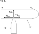
- FIG. 3 is a conceptual diagram in the case where the temperature at the outer periphery of the wafer is higher than the temperature at the central portion, and FIG.
- Patent Document 1 not only makes the oxide film thickness distribution non-uniform by making the temperature distribution in the wafer surface non-uniform, but also the temperature difference between the wafer center and the outer periphery.
- the thermal stress resulting from this increases, and slip dislocation tends to occur from the outer periphery of the wafer.
- slip dislocation occurs remarkably from the periphery of the wafer at a high temperature exceeding 1250 ° C.
- the present invention has been made in view of the above problems, and when a silicon wafer is heat-treated, a wafer heat-treatment method capable of reliably suppressing slip dislocation generated from a wafer support position and implementing the same. It is an object of the present invention to provide a heat treatment apparatus that can perform this process, a silicon wafer that has significantly less slip dislocations generated from a wafer support position using this method, or at least does not penetrate the surface, and a method for manufacturing the same.
- the temperature of the first main surface supported by the support member is 1 to 25 ° C. higher than the temperature of the main surface (second main surface) opposite to the first main surface of the wafer.
- the present invention provides a heat treatment method for a wafer, characterized in that heat treatment is performed while controlling the heating source.
- heat treatment is performed while controlling the temperature of the first main surface of the wafer supported by the support member to be 1 to 25 ° C. higher than the temperature of the second main surface opposite to the first main surface.
- the thermal stress generated in the vicinity of the support member can be reduced, and the occurrence of slip dislocation can be reliably suppressed as compared with the prior art, and a heat-treated wafer with less slip dislocation can be obtained.
- the heat treatment at a predetermined temperature accompanied by rapid temperature increase / decrease is a temperature rising rate or a temperature decreasing rate of 5 to 250 ° C./second, preferably 20 to 150 ° C./second, more preferably 30 to 70 ° C./second.
- This is a heat treatment (RTA treatment) with rapid heating or rapid cooling.
- the predetermined temperature refers to a temperature range of 700 ° C. or higher and lower than the melting point of the wafer.
- the temperature of the first main surface is changed by changing the output ratio between the first heating source for heating the first main surface of the wafer and the second heating source for heating the second main surface.
- the temperature is preferably controlled to be 1 to 25 ° C. higher than the temperature of the second main surface.
- the temperature can be controlled to be 1 to 25 ° C. higher than As a result, the temperature of the first main surface can be easily and reliably controlled to be 1 to 25 ° C. higher than the temperature of the second main surface, and the occurrence of slip dislocation can be suppressed more reliably.
- a halogen lamp can be used as the first heating source and the second heating source, and the output of the second heating source can be 10 to 90% of the output of the first heating source.
- the first heating source can be more easily and reliably performed.
- the temperature of the main surface can be controlled to be 1 to 25 ° C. higher than the temperature of the second main surface, and the occurrence of slip dislocation can be more effectively suppressed.
- a halogen lamp can be used as the heating source.
- a halogen lamp as a heating source, rapid heating can be easily performed, and heat treatment can be performed more easily.
- the support member horizontally supports the outer peripheral portion of the wafer by a plurality of support points.
- a wafer support member there is a method in which the edge portion of the wafer is supported by a thin ring-shaped susceptor over the entire circumference, but the wafer heat treatment method of the present invention is particularly effective when the wafer outer circumference portion is supported by a plurality of support points. is there.
- the predetermined temperature may be 700 ° C. or higher and lower than 1150 ° C.
- Slip dislocation from the position where the support member is located is noticeably generated when the heat treatment temperature is 700 ° C. or higher, but the wafer heat treatment method of the present invention is noticeably generated at such a treatment temperature of 700 ° C. or higher. This is particularly effective for suppressing slip dislocation.
- the said predetermined temperature can be made into 1150 degreeC or more and less than 1250 degreeC.
- a method for controlling an oxygen precipitate by performing an RTA process on the silicon wafer has been disclosed (see, for example, Japanese Patent Application Laid-Open No. 2001-503209) and is being widely adopted.
- most of the processing temperature of the RTA processing is 1150 ° C. or higher and lower than 1250 ° C. Since the occurrence of slip dislocation becomes more prominent at such a high temperature, the wafer heat treatment method of the present invention is more effective when RTA treatment is performed at 1150 ° C. or more and less than 1250 ° C.
- the said predetermined temperature can be made into 1250 degreeC or more.
- a method for melting glow-in defects (for example, COP) by RTA treatment at a temperature higher than 1300 ° C. has been disclosed (for example, see JP-A-2010-40589).
- the RTA temperature is less than 1250 ° C.
- slip dislocation occurs from the support position on the support member, but since it does not penetrate to the surface, it has a direct adverse effect on the device characteristics. There is not much.
- the heat treatment method for a wafer of the present invention can be particularly suitably performed even when the temperature is lower than 1250 ° C. At 1250 ° C. or higher, slip dislocation generated from the position of the support member penetrates to the surface, which has a significant adverse effect on device characteristics.
- the wafer heat treatment method of the present invention even if slip dislocation occurs, slip dislocation does not penetrate the surface, and many slip dislocations can be stopped in the bulk. It can be assumed that no dislocation occurs in the range of several ⁇ m.
- the wafer heat treatment method of the present invention is particularly effective when heat treatment is performed at a temperature of 1250 ° C. or higher.
- At least a silicon single crystal rod is grown by the Czochralski method, the silicon single crystal rod is sliced and processed into a silicon single crystal substrate, and then the present invention is applied to the silicon single crystal substrate.
- a method for producing a silicon wafer is provided, wherein the heat treatment is performed by the wafer heat treatment method described.
- the wafer heat treatment method of the present invention can surely suppress the occurrence of slip dislocation, the silicon wafer manufacturing method using the method can significantly reduce slip dislocation compared to the conventional method. Therefore, it becomes possible to manufacture a silicon wafer having a good quality more efficiently than before.
- a silicon wafer which is a silicon wafer that is heat-treated by the wafer heat treatment method described in the present invention.
- the silicon wafer to which the wafer heat treatment method of the present invention has been applied is of good quality with the slip dislocation greatly reduced as compared with the prior art.
- a heat treatment apparatus for performing heat treatment at a predetermined temperature accompanied with rapid temperature increase / decrease on a wafer, comprising at least a chamber for housing the wafer, and a first main surface of the wafer.
- a supporting member to be supported; a first heating source for heating the first main surface of the wafer; and a second heating for heating a main surface (second main surface) opposite to the first main surface of the wafer.
- a control mechanism for independently controlling outputs of the first heating source and the second heating source, and the control mechanism outputs outputs of the first heating source and the second heating source.
- the output is set so that the temperature of the first main surface supported by the support member is 1 to 25 ° C. higher than the temperature of the main surface (second main surface) opposite to the first main surface of the wafer. It is characterized by being controlled independently To provide a processing apparatus.
- the thermal stress in the vicinity of the support member in the wafer during the heat treatment can be reduced compared to the conventional case, and the occurrence rate of slip dislocation that has occurred in the wafer after the heat treatment can be greatly reduced. And a device capable of obtaining a wafer with less slip dislocation.
- the first and second heating sources are preferably halogen lamps.
- a halogen lamp as the heating source, rapid heating can be easily performed, and it becomes easier to perform a heat treatment that controls the temperature of the first main surface higher than the temperature of the second main surface.
- a method for heat-treating a wafer capable of surely suppressing slip dislocation generated from the wafer support position and a heat-treating apparatus capable of carrying out the same. And a silicon wafer in which slip dislocation generated from a wafer supporting position using this method is significantly less than that in the prior art, or at least does not penetrate the surface, and a method for manufacturing the same are provided.
- FIG. 4 is a conceptual diagram when performing heat treatment while controlling the heat source so that the temperature of the first main surface contacting the support member supporting the wafer of the present invention is 1 to 25 ° C. higher than the temperature of the second main surface. . It is the figure which showed an example of the outline of the heat processing apparatus of this invention. It is a conceptual diagram in case the temperature of the wafer outer peripheral part in the conventional heat processing method is higher than the temperature of center part. It is a conceptual diagram when the temperature of the wafer center part in the conventional heat processing method is higher than the temperature of an outer peripheral part. It is a conceptual diagram at the time of heat-processing by making the temperature of the 1st main surface which contacts the supporting member which supports the conventional wafer equal to the temperature of the 2nd main surface.
- FIG. 2 is a diagram showing an example of the outline of the heat treatment apparatus of the present invention.
- a heat treatment apparatus 10 of the present invention for performing heat treatment (RTA treatment) at a predetermined temperature with rapid temperature increase / decrease on a wafer W is made of at least quartz for accommodating the wafer W.
- the chamber 11 is provided with a temperature measurement special window (not shown).
- the pyrometer 19 installed outside the chamber 11 can measure the temperature of the wafer W through the special window. This signal can be transmitted to the control mechanism 15.
- the pyrometer 19 includes a first pyrometer 19a that measures the temperature of the first main surface of the wafer W and a second pyrometer 19b that measures the temperature of the second main surface. It may be transmitted.
- the control mechanism 15 then controls the power supply devices 21a (for controlling the first heating source 14a) and 21b (for controlling the second heating source 14b) according to the difference between the set temperature and the actually measured wafer temperature or the power ratio set in advance in the recipe. ) To control the outputs of the first heating source 14a and the second heating source 14b so that the temperature of the first main surface supported by the support member 12 is 1 to 25 ° C. higher than the temperature of the second main surface. The output can be controlled.
- a quartz buffer 18 is provided on the gas inlet 20a side of the quartz tray 16, and an introduced gas such as an oxidizing gas, a nitriding gas, or an Ar gas is supplied to the wafer W. It is possible to prevent hitting directly.
- an auto shutter 17 is provided to block outside air.
- the auto shutter 17 is provided with a wafer insertion port (not shown) that can be opened and closed by a gate valve. Further, the auto shutter 17 is provided with a gas exhaust port 20b so that the furnace atmosphere can be adjusted.
- the output of the heating source 14b is controlled independently by the control mechanism 15 that controls the output independently so that the temperature of the first main surface is 1 to 25 ° C. higher than the temperature of the second main surface.
- the heat flow inside the wafer can generate not only the heat flow toward the support member but also the heat flow flowing toward the wafer surface. And since this heat flow exists, the temperature gradient in the vicinity of the support member is reduced, and the thermal stress in the vicinity of the support member can be reduced as compared with the conventional case.
- the following method is also conceivable as a method of controlling the temperature so that the temperature of the first main surface is 1 to 25 ° C. higher than the temperature of the second main surface.
- the pyrometer 19a for measuring the temperature of the first main surface is provided, the RTA treatment is performed in advance in an oxygen atmosphere using the pyrometer 19a, and the relationship between the output of the heating source, the temperature, and the oxide film thickness is obtained.
- the outputs of the first heating source 14a and the second heating source 14b can be determined so that the temperature difference between the first main surface and the second main surface becomes a predetermined temperature difference.
- the output per lamp of the first heating source 14a and the second heating source 14b can be constant, and the lamp number ratio of the first heating source 14a and the second heating source 14b can be changed.
- the types of lamps of the first heating source 14a and the second heating source 14b lamps having different light emission characteristics
- the light emission characteristics are different even if the supplied power is constant.
- the first heating source 14a It is also possible to change the output ratio of the second heating source 14b.
- a feature of the heat treatment method of the present invention is that when a heat treatment is performed at a predetermined temperature accompanied by rapid temperature increase / decrease by heating a wafer represented by a silicon wafer with a heating source in a state of being supported by the support member, Heat treatment is performed while controlling the heating source so that the temperature of the supported first main surface is 1 to 25 ° C. higher than the temperature of the main surface (second main surface) opposite to the first main surface of the wafer. It is.
- the heat treatment is performed while controlling the heat source so that the temperature of the first main surface in contact with the support member supporting the wafer is 1 to 25 ° C. higher than the temperature of the second main surface.
- FIG. 5 is a conceptual diagram when heat treatment is performed with the temperature of the first main surface in contact with the support member supporting the wafer equal to the temperature of the second main surface as in the prior art.
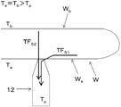
- the heat flow caused by the temperature difference is (1) heat flow TF 51 flowing toward the supporting member 12 from the first major surface W a (2) Heat flow TF 52 flowing from the second main surface W b toward the support member 12
- the following two types mainly occur. For this reason, it is considered that the temperature gradient in the vicinity of the support member 12 is increased, a large thermal stress is generated, and slip dislocation occurs.
- a distance and the temperature T b of the second main surface W b of the silicon wafer W, from the contact position in the first main surface W a of the supporting member 12 and the silicon wafer W and the temperature T a of the first main surface W a of the silicon wafer was, when the temperature of the silicon wafer W in the contact position of the first main surface W a and the support member 12 and T p, T a> T b > T p The relationship is established.
- the heat flow caused by the temperature difference is (1) heat flow TF 11 flowing toward the supporting member 12 from the first major surface W a (2) Heat flow TF 13 flowing from the first main surface W a toward the second main surface W b (3) Heat flow TF 12 flowing from the bulk portion of the wafer W toward the support member 12 (4) the heat flow through the bulk portion of the wafer W toward the second main surface W b TF 14
- the temperature gradient in the vicinity of the support member 12 becomes smaller than in the conventional case, and the thermal stress is reduced, so that it is considered that the occurrence of slip dislocation can be reliably suppressed.
- the heat flow TF 13 flowing from the first main surface W a toward the second main surface W b mechanism of suppressing slip dislocation occurs because the heat flow TF 14 flowing from the wafer bulk portion toward the second main surface W b is reduced not work almost can hardly suppress the generation of slip dislocation.
- the temperature difference between the temperature and the second main surface W b of the first main surface W a of the wafer W is greater than 25 ° C.
- the temperature difference between the first main surface W a and a second main surface W b is increased Therefore, the heat flows TF13 and TF14 in the wafer are increased, and the thermal stress generated in the wafer is increased, making it difficult to suppress the occurrence of slip dislocations. Therefore, it is necessary to perform heat treatment while controlling the temperature of the first main surface of the wafer supported by the support member to be 1 to 25 ° C. higher than the temperature of the second main surface opposite to the first main surface. .
- heat treatment is performed while controlling the temperature of the first main surface of the wafer supported by the support member to be 1 to 25 ° C. higher than the temperature of the second main surface opposite to the first main surface. Therefore, as described above, during the heat treatment, not only the heat flow toward the support member but also the heat flow flowing toward the surface exists, and the temperature gradient in the vicinity of the support member becomes small. Therefore, the thermal stress generated in the vicinity of the support member is reduced, whereby the occurrence of slip dislocation can be remarkably suppressed as compared with the conventional case, and a wafer with less slip dislocation can be obtained.
- the first heat source 14a for heating the first main surface W a of the wafer W by changing the output ratio between the second heating source 14b to heat the second main surface W b, the first main surface W the temperature of a can be controlled to be higher 1 ⁇ 25 ° C. than the temperature of the second main surface W b.
- the first main surface of the wafer is stably and surely changed.
- the temperature can be controlled to be 1 to 25 ° C. higher than the temperature of the second main surface, and the occurrence of slip dislocation can be suppressed more stably and reliably.
- a halogen lamp can be used as the heating source 13, particularly the first heating source 14a and the second heating source 14b.
- the output of the second heating source 14b can be 10 to 90% of the output of the first heating source 14a.
- the support member 12 can horizontally support the outer peripheral portion of the wafer W by a plurality of support points.
- the wafer heat treatment method of the present invention can suppress the occurrence of slip dislocation even when the wafer outer peripheral portion is supported by a plurality of support points.
- a susceptor of a type that is horizontally supported by a support point can be preferably used.
- the predetermined temperature for heating the wafer can be any temperature of 700 ° C. or higher and lower than 1150 ° C., 1150 ° C. or higher and lower than 1250 ° C., or 1250 ° C. or higher (desirably lower than the melting point temperature of the wafer).
- the wafer heat treatment method of the present invention that can reliably suppress the occurrence of slip dislocation can reliably suppress the occurrence of slip dislocation that occurs at a processing temperature of 700 ° C. or higher. This is preferable because it is possible.
- the treatment temperature is often 1150 ° C. or more and less than 1250 ° C.
- the temperature becomes high the occurrence of slip dislocation is remarkable. become.
- the wafer heat treatment method of the present invention can be used particularly effectively.
- glow-in defects such as COP
- the heat treatment method for a wafer of the present invention that can reliably suppress the occurrence of slip dislocations, This is particularly effective when heat treatment is performed at a temperature of 1250 ° C. or more at which slip dislocations generated from the position of the support member easily penetrate to the surface.
- a silicon single crystal rod is grown by the Czochralski method, the silicon single crystal rod is sliced and processed into a silicon single crystal substrate, and then the silicon single crystal substrate is heat treated by the wafer heat treatment method according to the present invention.
- the wafer heat treatment method according to the present invention.
- the silicon single crystal substrate to be manufactured may be a general one, and there are no particular limitations on electrical characteristics such as conductivity type and resistivity, crystal orientation, crystal diameter, and the like.
- the present invention is particularly effective in the heat treatment of a large-diameter wafer having a diameter of 8 inches (200 mm), 12 inches (300 mm), or more because its own weight becomes heavier and slip dislocation is more likely to occur.
- the processing from the silicon single crystal rod to the silicon single crystal substrate may be general, and for example, it can be sliced by a cutting device such as an inner peripheral slicer or a wire saw. Further, lapping, etching, polishing, etc. can be performed under general conditions, and can be appropriately selected according to the specifications of the silicon wafer to be manufactured.
- Example 1-5 Comparative Example 1-3
- Helios manufactured by Mattson Corp. was used as a heat treatment apparatus for rapidly raising and lowering the temperature.
- the apparatus has a control mechanism in which the lamp output of the upper lamp module (halogen lamp) corresponding to the second heating source and the lower lamp module (halogen lamp) corresponding to the first heating source can be changed at an arbitrary ratio.
- a p-type silicon wafer having a diameter of 300 mm was prepared, carried into the chamber through the opening of the heat treatment apparatus, and placed horizontally on three quartz support pins. At this time, the side supported by the support pins was the first main surface, and the opposite side was the second main surface.
- oxygen gas was introduced into the chamber, the temperature was raised to a predetermined heat treatment temperature at 50 ° C./sec, and heat treatment was performed at predetermined temperatures (1200 ° C., 1250 ° C., 1300 ° C., 1350 ° C.) for 10 seconds, respectively. Thereafter, heating was turned off at a stage where the temperature was lowered to 800 ° C. at a temperature lowering rate of 50 ° C./sec, and then cooled to 500 ° C. in the chamber, and then the wafer was taken out.
- the oxide film thicknesses of the first main surface and the second main surface were measured with an ellipsometer, and the temperature difference between the first main surface and the second main surface was calculated from the film thickness. Further, slip dislocation measurement on the wafer surface (second main surface) was performed with a laser scattering type foreign material inspection apparatus (SP1 manufactured by KLA-Tencor). The results are shown in Table 1.
- ⁇ means that slip dislocation does not occur at any of the three support pin positions
- ⁇ means that one or two slip dislocations occur
- x means that slip dislocation occurs in all three positions.
- the wafer heat-treated by the method of Example 1-5 compared to Comparative Example 1-3 has a shorter slip dislocation, which prevents or reduces slip dislocation. It was confirmed that there was an effect.
- Example 6 Helios manufactured by Mattson Corp. was used as a heat treatment apparatus for rapidly raising and lowering the temperature.
- the apparatus has a control mechanism in which the lamp output of the upper lamp module (halogen lamp) corresponding to the second heating source and the lower lamp module (halogen lamp) corresponding to the first heating source can be changed at an arbitrary ratio.
- a p-type silicon wafer having a diameter of 300 mm was prepared, carried into the chamber through the opening of the RTA apparatus, and placed horizontally on three quartz support pins. At this time, the side supported by the support pins was the first main surface, and the opposite side was the second main surface.
- oxygen gas was introduced into the chamber, the temperature was raised to a predetermined heat treatment temperature at 50 ° C./sec, and heat treatment was performed at predetermined temperatures (700 ° C., 1100 ° C., 1300 ° C.) for 10 seconds, respectively. Thereafter, heating was turned off at a stage where the temperature was lowered to 800 ° C. at a temperature lowering rate of 50 ° C./sec, and then cooled to 500 ° C. in the chamber, and then the wafer was taken out.
- upper side: lower side 40: 100 (temperature difference of 15 ° C.), the temperature at the outer periphery of the wafer and the temperature at the center were the same.
- the present invention is not limited to the above embodiment.
- the above-described embodiment is an exemplification, and the present invention has any configuration that has substantially the same configuration as the technical idea described in the claims of the present invention and exhibits the same function and effect. Are included in the technical scope.
Landscapes
- Engineering & Computer Science (AREA)
- Chemical & Material Sciences (AREA)
- Physics & Mathematics (AREA)
- Power Engineering (AREA)
- Computer Hardware Design (AREA)
- Microelectronics & Electronic Packaging (AREA)
- Manufacturing & Machinery (AREA)
- Condensed Matter Physics & Semiconductors (AREA)
- General Physics & Mathematics (AREA)
- Materials Engineering (AREA)
- Metallurgy (AREA)
- Organic Chemistry (AREA)
- Crystallography & Structural Chemistry (AREA)
- Thermal Sciences (AREA)
- Health & Medical Sciences (AREA)
- Toxicology (AREA)
- Crystals, And After-Treatments Of Crystals (AREA)
- Container, Conveyance, Adherence, Positioning, Of Wafer (AREA)
Priority Applications (4)
| Application Number | Priority Date | Filing Date | Title |
|---|---|---|---|
| CN201180039907.3A CN103069545B (zh) | 2010-08-18 | 2011-07-15 | 晶片的热处理方法、硅晶片的制造方法、硅晶片及热处理装置 |
| US13/807,243 US20130098888A1 (en) | 2010-08-18 | 2011-07-15 | Method for heat-treating wafer, method for producing silicon wafer, silicon wafer, and heat treatment apparatus |
| EP11817884.7A EP2608248A4 (en) | 2010-08-18 | 2011-07-15 | THERMAL PROCESSING METHOD FOR WAFER, METHOD FOR PRODUCING SILICON WAFER, SILICON WAFER, AND HEAT TREATMENT APPARATUS |
| KR1020137004020A KR101658892B1 (ko) | 2010-08-18 | 2011-07-15 | 웨이퍼의 열처리 방법 및 실리콘 웨이퍼의 제조 방법 및 실리콘 웨이퍼 및 열처리 장치 |
Applications Claiming Priority (2)
| Application Number | Priority Date | Filing Date | Title |
|---|---|---|---|
| JP2010-183020 | 2010-08-18 | ||
| JP2010183020A JP5530856B2 (ja) | 2010-08-18 | 2010-08-18 | ウエーハの熱処理方法及びシリコンウエーハの製造方法並びに熱処理装置 |
Publications (1)
| Publication Number | Publication Date |
|---|---|
| WO2012023233A1 true WO2012023233A1 (ja) | 2012-02-23 |
Family
ID=45604904
Family Applications (1)
| Application Number | Title | Priority Date | Filing Date |
|---|---|---|---|
| PCT/JP2011/004047 WO2012023233A1 (ja) | 2010-08-18 | 2011-07-15 | ウエーハの熱処理方法及びシリコンウエーハの製造方法並びにシリコンウエーハ並びに熱処理装置 |
Country Status (7)
Families Citing this family (3)
| Publication number | Priority date | Publication date | Assignee | Title |
|---|---|---|---|---|
| JP6138610B2 (ja) * | 2013-07-10 | 2017-05-31 | 株式会社Screenホールディングス | 熱処理装置 |
| KR20220162896A (ko) * | 2021-06-01 | 2022-12-09 | 삼성디스플레이 주식회사 | 레이저 가공 장치 및 레이저 가공 방법 |
| JP2024162803A (ja) * | 2023-05-11 | 2024-11-21 | グローバルウェーハズ・ジャパン株式会社 | 半導体ウェーハの製造方法および半導体デバイスの製造方法 |
Citations (7)
| Publication number | Priority date | Publication date | Assignee | Title |
|---|---|---|---|---|
| JPH0245914A (ja) * | 1988-08-05 | 1990-02-15 | Nec Yamaguchi Ltd | 半導体基板の予備加熱装置 |
| JP2001503009A (ja) | 1997-04-09 | 2001-03-06 | エムイーエムシー・エレクトロニック・マテリアルズ・インコーポレイテッド | 低欠陥密度の理想的酸素析出シリコン |
| JP2008016652A (ja) * | 2006-07-06 | 2008-01-24 | Shin Etsu Handotai Co Ltd | シリコンウェーハの製造方法 |
| JP2010034288A (ja) | 2008-07-29 | 2010-02-12 | Sumco Corp | シリコンウェーハの熱処理方法 |
| JP2010040589A (ja) | 2008-07-31 | 2010-02-18 | Covalent Materials Corp | シリコンウェーハの製造方法 |
| JP2010073782A (ja) * | 2008-09-17 | 2010-04-02 | Sumco Corp | 半導体ウェーハの熱処理方法 |
| JP2010109100A (ja) * | 2008-10-29 | 2010-05-13 | Shin Etsu Handotai Co Ltd | シリコンウェーハの製造方法 |
Family Cites Families (12)
| Publication number | Priority date | Publication date | Assignee | Title |
|---|---|---|---|---|
| JPS63221612A (ja) * | 1987-03-10 | 1988-09-14 | Mitsubishi Electric Corp | ランプアニ−ル装置 |
| JPH0917742A (ja) * | 1995-06-30 | 1997-01-17 | Hitachi Ltd | 熱処理装置 |
| DE19727693A1 (de) * | 1997-06-20 | 1998-12-24 | Heidenhain Gmbh Dr Johannes | Verfahren und Vorrichtung zur Herstellung elektrisch leitfähiger Durchgänge in Halbleiter-Bauelementen |
| JPH1197448A (ja) * | 1997-09-18 | 1999-04-09 | Kemitoronikusu:Kk | 熱処理装置とこれを用いた半導体結晶の熱処理法 |
| JPH11214501A (ja) * | 1998-01-26 | 1999-08-06 | Mitsubishi Electric Corp | 半導体デバイスの製造方法、半導体デバイス及び半導体デバイスの製造装置 |
| US6849831B2 (en) * | 2002-03-29 | 2005-02-01 | Mattson Technology, Inc. | Pulsed processing semiconductor heating methods using combinations of heating sources |
| JP5630935B2 (ja) * | 2003-12-19 | 2014-11-26 | マトソン テクノロジー、インコーポレイテッド | 工作物の熱誘起運動を抑制する機器及び装置 |
| JP5084108B2 (ja) * | 2005-03-15 | 2012-11-28 | ラピスセミコンダクタ株式会社 | 半導体装置の製造方法 |
| US8530801B2 (en) * | 2005-07-06 | 2013-09-10 | Sumco Techxiv Kabushiki Kaisha | Method and apparatus for manufacturing semiconductor wafer |
| JP5239155B2 (ja) * | 2006-06-20 | 2013-07-17 | 信越半導体株式会社 | シリコンウエーハの製造方法 |
| JP2008117892A (ja) * | 2006-11-02 | 2008-05-22 | Toshiba Corp | 半導体製造装置および半導体装置の製造方法 |
| JP4816634B2 (ja) * | 2007-12-28 | 2011-11-16 | ウシオ電機株式会社 | 基板加熱装置及び基板加熱方法 |
-
2010
- 2010-08-18 JP JP2010183020A patent/JP5530856B2/ja active Active
-
2011
- 2011-07-15 WO PCT/JP2011/004047 patent/WO2012023233A1/ja active Application Filing
- 2011-07-15 EP EP11817884.7A patent/EP2608248A4/en not_active Withdrawn
- 2011-07-15 KR KR1020137004020A patent/KR101658892B1/ko active Active
- 2011-07-15 US US13/807,243 patent/US20130098888A1/en not_active Abandoned
- 2011-07-15 CN CN201180039907.3A patent/CN103069545B/zh active Active
- 2011-07-21 TW TW100125842A patent/TWI508180B/zh active
Patent Citations (7)
| Publication number | Priority date | Publication date | Assignee | Title |
|---|---|---|---|---|
| JPH0245914A (ja) * | 1988-08-05 | 1990-02-15 | Nec Yamaguchi Ltd | 半導体基板の予備加熱装置 |
| JP2001503009A (ja) | 1997-04-09 | 2001-03-06 | エムイーエムシー・エレクトロニック・マテリアルズ・インコーポレイテッド | 低欠陥密度の理想的酸素析出シリコン |
| JP2008016652A (ja) * | 2006-07-06 | 2008-01-24 | Shin Etsu Handotai Co Ltd | シリコンウェーハの製造方法 |
| JP2010034288A (ja) | 2008-07-29 | 2010-02-12 | Sumco Corp | シリコンウェーハの熱処理方法 |
| JP2010040589A (ja) | 2008-07-31 | 2010-02-18 | Covalent Materials Corp | シリコンウェーハの製造方法 |
| JP2010073782A (ja) * | 2008-09-17 | 2010-04-02 | Sumco Corp | 半導体ウェーハの熱処理方法 |
| JP2010109100A (ja) * | 2008-10-29 | 2010-05-13 | Shin Etsu Handotai Co Ltd | シリコンウェーハの製造方法 |
Non-Patent Citations (1)
| Title |
|---|
| See also references of EP2608248A4 |
Also Published As
| Publication number | Publication date |
|---|---|
| CN103069545A (zh) | 2013-04-24 |
| KR101658892B1 (ko) | 2016-09-23 |
| TWI508180B (zh) | 2015-11-11 |
| TW201220403A (en) | 2012-05-16 |
| US20130098888A1 (en) | 2013-04-25 |
| KR20130100987A (ko) | 2013-09-12 |
| CN103069545B (zh) | 2016-03-02 |
| JP5530856B2 (ja) | 2014-06-25 |
| JP2012043931A (ja) | 2012-03-01 |
| EP2608248A1 (en) | 2013-06-26 |
| EP2608248A4 (en) | 2014-05-07 |
Similar Documents
| Publication | Publication Date | Title |
|---|---|---|
| US7977219B2 (en) | Manufacturing method for silicon wafer | |
| JP6044660B2 (ja) | シリコンウェーハの製造方法 | |
| JP5504664B2 (ja) | シリコンエピタキシャルウェーハおよびその製造方法 | |
| JP5567259B2 (ja) | シリコンウェーハおよびその製造方法 | |
| JP5470769B2 (ja) | シリコンウェーハの熱処理方法 | |
| JP5530856B2 (ja) | ウエーハの熱処理方法及びシリコンウエーハの製造方法並びに熱処理装置 | |
| WO2020080247A1 (ja) | シリコンウェーハの熱処理方法 | |
| JP5512137B2 (ja) | シリコンウェーハの熱処理方法 | |
| WO2002045141A1 (fr) | Procédé de fabrication de plaquettes à semi-conducteur | |
| JP6489321B2 (ja) | エピタキシャルウェーハの製造方法 | |
| JP2008166517A (ja) | 半導体基板の製造方法 | |
| JP5613994B2 (ja) | シリコンウェーハおよびその製造方法 | |
| JP5410769B2 (ja) | シリコンウェーハの熱処理方法 | |
| JP5517354B2 (ja) | シリコンウェーハの熱処理方法 | |
| JP5517235B2 (ja) | シリコンウエハの熱処理方法 | |
| TWI867950B (zh) | 半導體晶圓的製造方法以及半導體器件的製造方法 | |
| JP5109588B2 (ja) | 熱処理装置 | |
| JP5811218B2 (ja) | シリコンエピタキシャルウェーハの製造方法 | |
| TWI891224B (zh) | 半導體晶圓的製造方法以及半導體器件的製造方法 | |
| JP2010040806A (ja) | シリコンウェーハの熱処理方法 | |
| US20240363363A1 (en) | Method of manufacturing semiconductor wafer and semiconductor device | |
| KR100685260B1 (ko) | 실리콘 웨이퍼의 열처리 방법 | |
| JP7051560B2 (ja) | シリコンウェーハの熱処理方法 | |
| JP2010027995A (ja) | 枚葉式熱処理装置のプロセスチャンバーの冷却方法 |
Legal Events
| Date | Code | Title | Description |
|---|---|---|---|
| WWE | Wipo information: entry into national phase |
Ref document number: 201180039907.3 Country of ref document: CN |
|
| 121 | Ep: the epo has been informed by wipo that ep was designated in this application |
Ref document number: 11817884 Country of ref document: EP Kind code of ref document: A1 |
|
| WWE | Wipo information: entry into national phase |
Ref document number: 13807243 Country of ref document: US |
|
| ENP | Entry into the national phase |
Ref document number: 20137004020 Country of ref document: KR Kind code of ref document: A |
|
| NENP | Non-entry into the national phase |
Ref country code: DE |
|
| WWE | Wipo information: entry into national phase |
Ref document number: 2011817884 Country of ref document: EP |