WO2012017997A1 - 回路基板に実装する部品の固定金具 - Google Patents
回路基板に実装する部品の固定金具 Download PDFInfo
- Publication number
- WO2012017997A1 WO2012017997A1 PCT/JP2011/067628 JP2011067628W WO2012017997A1 WO 2012017997 A1 WO2012017997 A1 WO 2012017997A1 JP 2011067628 W JP2011067628 W JP 2011067628W WO 2012017997 A1 WO2012017997 A1 WO 2012017997A1
- Authority
- WO
- WIPO (PCT)
- Prior art keywords
- solder
- circuit board
- groove
- solder joint
- plate portion
- Prior art date
- Legal status (The legal status is an assumption and is not a legal conclusion. Google has not performed a legal analysis and makes no representation as to the accuracy of the status listed.)
- Ceased
Links
Images


Classifications
-
- H—ELECTRICITY
- H05—ELECTRIC TECHNIQUES NOT OTHERWISE PROVIDED FOR
- H05K—PRINTED CIRCUITS; CASINGS OR CONSTRUCTIONAL DETAILS OF ELECTRIC APPARATUS; MANUFACTURE OF ASSEMBLAGES OF ELECTRICAL COMPONENTS
- H05K1/00—Printed circuits
- H05K1/18—Printed circuits structurally associated with non-printed electric components
- H05K1/181—Printed circuits structurally associated with non-printed electric components associated with surface mounted components
-
- H—ELECTRICITY
- H01—ELECTRIC ELEMENTS
- H01R—ELECTRICALLY-CONDUCTIVE CONNECTIONS; STRUCTURAL ASSOCIATIONS OF A PLURALITY OF MUTUALLY-INSULATED ELECTRICAL CONNECTING ELEMENTS; COUPLING DEVICES; CURRENT COLLECTORS
- H01R12/00—Structural associations of a plurality of mutually-insulated electrical connecting elements, specially adapted for printed circuits, e.g. printed circuit boards [PCB], flat or ribbon cables, or like generally planar structures, e.g. terminal strips, terminal blocks; Coupling devices specially adapted for printed circuits, flat or ribbon cables, or like generally planar structures; Terminals specially adapted for contact with, or insertion into, printed circuits, flat or ribbon cables, or like generally planar structures
- H01R12/50—Fixed connections
- H01R12/51—Fixed connections for rigid printed circuits or like structures
- H01R12/55—Fixed connections for rigid printed circuits or like structures characterised by the terminals
- H01R12/57—Fixed connections for rigid printed circuits or like structures characterised by the terminals surface mounting terminals
-
- H—ELECTRICITY
- H01—ELECTRIC ELEMENTS
- H01R—ELECTRICALLY-CONDUCTIVE CONNECTIONS; STRUCTURAL ASSOCIATIONS OF A PLURALITY OF MUTUALLY-INSULATED ELECTRICAL CONNECTING ELEMENTS; COUPLING DEVICES; CURRENT COLLECTORS
- H01R12/00—Structural associations of a plurality of mutually-insulated electrical connecting elements, specially adapted for printed circuits, e.g. printed circuit boards [PCB], flat or ribbon cables, or like generally planar structures, e.g. terminal strips, terminal blocks; Coupling devices specially adapted for printed circuits, flat or ribbon cables, or like generally planar structures; Terminals specially adapted for contact with, or insertion into, printed circuits, flat or ribbon cables, or like generally planar structures
- H01R12/70—Coupling devices
- H01R12/7005—Guiding, mounting, polarizing or locking means; Extractors
- H01R12/7011—Locking or fixing a connector to a PCB
- H01R12/707—Soldering or welding
-
- H—ELECTRICITY
- H05—ELECTRIC TECHNIQUES NOT OTHERWISE PROVIDED FOR
- H05K—PRINTED CIRCUITS; CASINGS OR CONSTRUCTIONAL DETAILS OF ELECTRIC APPARATUS; MANUFACTURE OF ASSEMBLAGES OF ELECTRICAL COMPONENTS
- H05K3/00—Apparatus or processes for manufacturing printed circuits
- H05K3/30—Assembling printed circuits with electric components, e.g. with resistors
- H05K3/303—Assembling printed circuits with electric components, e.g. with resistors with surface mounted components
-
- H—ELECTRICITY
- H05—ELECTRIC TECHNIQUES NOT OTHERWISE PROVIDED FOR
- H05K—PRINTED CIRCUITS; CASINGS OR CONSTRUCTIONAL DETAILS OF ELECTRIC APPARATUS; MANUFACTURE OF ASSEMBLAGES OF ELECTRICAL COMPONENTS
- H05K2201/00—Indexing scheme relating to printed circuits covered by H05K1/00
- H05K2201/09—Shape and layout
- H05K2201/09209—Shape and layout details of conductors
- H05K2201/09654—Shape and layout details of conductors covering at least two types of conductors provided for in H05K2201/09218 - H05K2201/095
- H05K2201/09781—Dummy conductors, i.e. not used for normal transport of current; Dummy electrodes of components
-
- H—ELECTRICITY
- H05—ELECTRIC TECHNIQUES NOT OTHERWISE PROVIDED FOR
- H05K—PRINTED CIRCUITS; CASINGS OR CONSTRUCTIONAL DETAILS OF ELECTRIC APPARATUS; MANUFACTURE OF ASSEMBLAGES OF ELECTRICAL COMPONENTS
- H05K2201/00—Indexing scheme relating to printed circuits covered by H05K1/00
- H05K2201/10—Details of components or other objects attached to or integrated in a printed circuit board
- H05K2201/10007—Types of components
- H05K2201/10189—Non-printed connector
-
- H—ELECTRICITY
- H05—ELECTRIC TECHNIQUES NOT OTHERWISE PROVIDED FOR
- H05K—PRINTED CIRCUITS; CASINGS OR CONSTRUCTIONAL DETAILS OF ELECTRIC APPARATUS; MANUFACTURE OF ASSEMBLAGES OF ELECTRICAL COMPONENTS
- H05K2201/00—Indexing scheme relating to printed circuits covered by H05K1/00
- H05K2201/10—Details of components or other objects attached to or integrated in a printed circuit board
- H05K2201/10227—Other objects, e.g. metallic pieces
- H05K2201/1031—Surface mounted metallic connector elements
-
- H—ELECTRICITY
- H05—ELECTRIC TECHNIQUES NOT OTHERWISE PROVIDED FOR
- H05K—PRINTED CIRCUITS; CASINGS OR CONSTRUCTIONAL DETAILS OF ELECTRIC APPARATUS; MANUFACTURE OF ASSEMBLAGES OF ELECTRICAL COMPONENTS
- H05K3/00—Apparatus or processes for manufacturing printed circuits
- H05K3/30—Assembling printed circuits with electric components, e.g. with resistors
- H05K3/32—Assembling printed circuits with electric components, e.g. with resistors electrically connecting electric components or wires to printed circuits
- H05K3/34—Assembling printed circuits with electric components, e.g. with resistors electrically connecting electric components or wires to printed circuits by soldering
-
- Y—GENERAL TAGGING OF NEW TECHNOLOGICAL DEVELOPMENTS; GENERAL TAGGING OF CROSS-SECTIONAL TECHNOLOGIES SPANNING OVER SEVERAL SECTIONS OF THE IPC; TECHNICAL SUBJECTS COVERED BY FORMER USPC CROSS-REFERENCE ART COLLECTIONS [XRACs] AND DIGESTS
- Y02—TECHNOLOGIES OR APPLICATIONS FOR MITIGATION OR ADAPTATION AGAINST CLIMATE CHANGE
- Y02P—CLIMATE CHANGE MITIGATION TECHNOLOGIES IN THE PRODUCTION OR PROCESSING OF GOODS
- Y02P70/00—Climate change mitigation technologies in the production process for final industrial or consumer products
- Y02P70/50—Manufacturing or production processes characterised by the final manufactured product
Definitions
- the present invention relates to a fixture for fixing components such as a board-mounted connector on a circuit board by soldering.
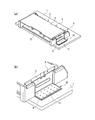
- FIG. 3 is a diagram showing a conventional fixing bracket
- FIG. 3 (a) is a perspective view of the fixing bracket
- FIG. 3 (b) is a state in which the connector is fixed on the circuit board using the fixing bracket. It is a perspective view shown.
- the fixing bracket 110 is a plate-like member bent in an L-shaped cross section that is attached to both side portions of a board mounting connector 102 (component mounted on the circuit board) mounted on the circuit board 101.
- 101 has a solder joint plate portion 111 soldered and fixed to the surface of the connector 101 using cream solder, and a component fixing portion 112 to be inserted and fixed to the metal fitting mounting portions 106 on both sides of the connector housing 103 of the connector 102.
- the connector 102 has a plurality of terminals 104 mounted on the rear wall portion of the connector housing 103 having a mating connector fitting port 105 on the front surface, and the front end of each terminal 104 is placed inside the fitting port 105 of the connector housing 103. It is mounted on the circuit board 101 by connecting the rear leg portion of each terminal 104 that is exposed and extends rearward of the connector housing 103 to the circuit conductor of the circuit board 101. Further, since the mounting strength is not sufficient by itself, the solder joint plate portion 111 of the fixing bracket 110 attached to both sides of the connector housing 103 is soldered onto the circuit board 1 using cream solder, thereby It is fixed on the substrate 101.
- solder joint plate portion 111 of the fixture 110 is divided into two joint legs 111A each having a U-shaped notch 113 so that the total length of the outer peripheral edges to be soldered is increased. .
- the conventional fixture 110 shown in FIGS. 3 (a) and 3 (b) has two joining legs 111A with U-shaped notches 113, so that the area to be joined with solder increases.
- the area to be joined with solder increases.
- an object of the present invention is to solve the above-described problems, and even when the area of the solder joint plate portion does not change, a sufficient amount of solder can be held on the entire solder joint surface. Accordingly, it is an object of the present invention to provide a fixing bracket for a component mounted on a circuit board, which can exhibit high bonding strength.
- the above object of the present invention can be achieved by the following constitution. (1) having a solder joint plate portion soldered and fixed to the surface of the circuit board using cream solder, and a component fixing portion fixed to a component to be mounted on the circuit board; A groove for sucking cream solder applied to the surface of the circuit board by capillary action is formed on the solder joint surface of the lower surface of the solder joint plate portion, and from the upper surface to the lower surface of the solder joint plate portion, A fixing bracket for a component that is mounted on a circuit board in which a plurality of communication holes that communicate with the groove and can suck up the cream solder by capillary action are spaced apart in the extending direction of the groove.
- the groove is formed as a V-groove having a tapered cross section, and the communication hole is formed in a tapered cross-section shape from the upper surface to the lower surface of the solder joint plate portion.
- the solder is sucked up inside the groove due to a capillary phenomenon, but the suction effect is weak only with the groove. Further, when a hole is formed in the solder joint plate portion, the solder is sucked into the hole by a capillary phenomenon, but the sucking effect is weak only with the hole.
- the solder is easily sucked up by the presence of the thin section in the middle of the path from the V groove to the communication hole. Accordingly, the amount of solder held on the solder joint surface is increased, and the joining force of the fixture is increased.
- the plurality of V grooves provided at intervals from each other extend from the outer peripheral edge of the solder joint plate portion toward the outer peripheral edge on the opposite side. Therefore, a sufficient amount of solder can be effectively spread over the entire solder joint surface.
- FIG. 1A is a perspective view
- FIG. 1B is a cross-sectional view taken along the line BB in FIG. 1A
- FIG. It is a perspective view of the part shown by (b).
- FIG. 2 (a) is a whole perspective view
- FIG.2 (b) is an expansion perspective view of the principal part.
- FIG. 3A is a perspective view of a fixing bracket
- FIG. 3B is a perspective view illustrating a state in which the connector is fixed on a circuit board using the fixing bracket. is there.
- FIG. 1 is a configuration diagram of a fixing metal fitting of the embodiment
- FIG. 1 (a) is a perspective view
- FIG. 1 (b) is a cross-sectional view taken along line BB in FIG. 1 (a)
- FIG. FIG. 2 is a perspective view of the portion shown in FIG. 2B
- FIG. 2 is a view showing a state where the board mounting connector is fixed on the circuit board using the fixing bracket
- FIG. 2A is an overall perspective view
- the fixing bracket 10 of this embodiment includes a board-mounted connector 2 (mounted on the circuit board 1).
- a solder joint plate portion 11 which is attached to both sides of a circuit board component) and which is bent and formed into an L-shaped cross section and is soldered and fixed to the surface of the circuit substrate 1 using cream solder.
- a component fixing portion 12 to be inserted and fixed to the metal fitting mounting portions 6 on both sides of the connector housing 3 of the connector 2.
- the connector 2 has a plurality of terminals 4 mounted on the rear wall portion of the connector housing 3 having a mating connector fitting port 5 on the front surface, and the front end of each terminal 4 is exposed inside the fitting port 5 of the connector housing 3.
- the rear legs of the terminals 4 extending rearward of the connector housing 3 are mounted on the circuit board 1 by connecting to the circuit conductors of the circuit board 1.
- the lower surface (solder bonding surface) 11B of the solder bonding plate portion 11 of the fixing bracket 10 mounted on both side portions of the connector housing 3 is used, and cream solder is used on the circuit board 1. And then soldered to the circuit board 1.
- the solder joint surface of the lower surface 11B of the solder joint plate portion 11 of the fixing bracket 10 is applied to the surface of the circuit board 1 by capillary action.
- a V-shaped groove 13 for sucking cream solder is formed, and a rectangular communication hole that communicates with the V-shaped groove 13 from the upper surface 11A to the lower surface 11B of the solder joint plate 11 and can suck cream solder by capillary action.
- a plurality of holes 14 are formed so as to be spaced apart in the direction in which the V-groove 13 extends.
- the V-groove 13 has a tapered V-shaped cross section, and the communication hole 14 is formed in a tapered cross-section shape from the upper surface 11A to the lower surface 11B of the solder joint plate portion 11.
- the tapered portion of the communication hole 14 communicates with the tapered portion of the V groove 13.
- the V-grooves 13 are spaced at a constant interval in the extending direction of the outer peripheral edge 11 ⁇ / b> C from a plurality of positions on the outer peripheral edge 11 ⁇ / b> C located far from the component fixing part 12 of the solder bonding plate part 11 toward the outer peripheral edge 11 ⁇ / b> E on the opposite side.
- the openings 14 are linearly formed parallel to each other, and the communication holes 14 are also arranged at regular intervals in the vertical and horizontal directions.
- soldering plate part 11 is joined on the land of the circuit board 1 by placing the joining plate part 11 and passing it through the reflow bath. At that time, a sufficient amount of solder can be sucked up by a capillary phenomenon by the combination of the V-groove 13 and the communication hole 14 formed in the solder joint plate portion 11, so that the solder joint surface (the solder joint plate portion 11 of the solder joint plate portion 11 can be sucked up). Solder can be sufficiently spread over the entire surface of the lower surface), and the bonding force after reflow can be increased.
- the solder when the V-groove 13 is formed on the solder joint surface, the solder is sucked up into the V-groove 13 by capillary action, but the sucking effect is weak with the V-groove 13 alone. Further, when the communication hole 14 is formed in the solder joint plate portion 11, the solder is sucked into the communication hole 14 due to a capillary phenomenon, but the suction effect is weak only with the communication hole 14.
- the presence of a thin section in the middle of the path from the V groove 13 to the communication hole 14 makes it easier for the solder to be sucked up. Therefore, the amount of solder held on the solder joint surface is increased, and the joining force of the fixture 10 is further increased.
- the solder can be effectively used from a wide area.
- a sufficient amount of solder can be effectively spread over the entire solder joint surface.
- the linear V groove 13 is provided on the lower surface 11B of the solder joint plate portion 11, a reinforcing action of the V groove 13 can be obtained, and the flatness of the solder joint plate portion 11 at the time of manufacture can be obtained. A decrease can be prevented.
- the groove is the V-groove 13
- a groove having another cross-sectional shape may be provided.
- the said embodiment described the case where the communicating hole 14 was a square hole, a circular hole may be sufficient.
Landscapes
- Engineering & Computer Science (AREA)
- Microelectronics & Electronic Packaging (AREA)
- Manufacturing & Machinery (AREA)
- Coupling Device And Connection With Printed Circuit (AREA)
- Multi-Conductor Connections (AREA)
- Connections Effected By Soldering, Adhesion, Or Permanent Deformation (AREA)
- Electric Connection Of Electric Components To Printed Circuits (AREA)
- Connection Of Plates (AREA)
Abstract
Description
図3はその従来例の固定金具を示す図で、図3(a)は固定金具の斜視図、図3(b)はその固定金具を用いてコネクタを回路基板上に固定している状態を示す斜視図である。
(1) 回路基板の表面にクリーム半田を用いて半田付け固定される半田接合板部と、前記回路基板上に実装しようとする部品に固定される部品固定部とを有し、
前記半田接合板部の下面の半田接合面に、毛細管現象により前記回路基板の表面に塗布されたクリーム半田を吸い上げる溝が形成されると共に、前記半田接合板部の上面から下面に向けて、前記溝に連通すると共に毛細管現象により前記クリーム半田を吸い上げることの可能な連通孔が、前記溝の延びる方向に離間して複数穿設されている回路基板に実装する部品の固定金具。
図1は実施形態の固定金具の構成図で、図1(a)は斜視図、図1(b)は図1(a)のB-B矢視断面図、図1(c)は図1(b)で示す部分の斜視図、図2は同固定金具を用いて基板実装コネクタを回路基板上に固定した状態を示す図で、図2(a)は全体斜視図、図2(b)はその要部の拡大斜視図である。
2 コネクタ(回路基板上に実装しようとする部品)
10 固定金具
11 半田接合板部
11A 上面
11B 下面
11C,11E 外周縁
12 部品固定部
13 V溝
14 連通孔
Claims (3)
- 回路基板の表面にクリーム半田を用いて半田付け固定される半田接合板部と、前記回路基板上に実装しようとする部品に固定される部品固定部とを有し、
前記半田接合板部の下面の半田接合面に、毛細管現象により前記回路基板の表面に塗布されたクリーム半田を吸い上げる溝が形成されると共に、前記半田接合板部の上面から下面に向けて、前記溝に連通すると共に毛細管現象により前記クリーム半田を吸い上げることの可能な連通孔が、前記溝の延びる方向に離間して複数穿設されている回路基板に実装する部品の固定金具。 - 前記溝が、先細り断面のV溝として形成されると共に、前記連通孔が、前記半田接合板部の上面から下面に向かうほど先窄まりの断面形状に形成され、前記V溝の先細り部分に前記連通孔の先窄まり部分が連通している請求項1に記載の回路基板に実装する部品の固定金具。
- 前記V溝が、前記半田接合板部の外周縁の複数箇所から反対側の外周縁に向けて互いに間隔を開けて直線的に形成されている請求項2に記載の回路基板に実装する部品の固定金具。
Priority Applications (3)
| Application Number | Priority Date | Filing Date | Title |
|---|---|---|---|
| US13/813,743 US9025338B2 (en) | 2010-08-02 | 2011-08-01 | Fixing fitting of parts mounted on circuit board |
| KR1020137002598A KR101553754B1 (ko) | 2010-08-02 | 2011-08-01 | 회로 보드에 장착된 구성품에 대한 고정 부품 |
| CN201180037854.1A CN103053080B (zh) | 2010-08-02 | 2011-08-01 | 安装在电路板上的部件的固定金具 |
Applications Claiming Priority (2)
| Application Number | Priority Date | Filing Date | Title |
|---|---|---|---|
| JP2010-173763 | 2010-08-02 | ||
| JP2010173763A JP5679548B2 (ja) | 2010-08-02 | 2010-08-02 | 回路基板に実装する部品の固定金具 |
Publications (1)
| Publication Number | Publication Date |
|---|---|
| WO2012017997A1 true WO2012017997A1 (ja) | 2012-02-09 |
Family
ID=45559494
Family Applications (1)
| Application Number | Title | Priority Date | Filing Date |
|---|---|---|---|
| PCT/JP2011/067628 Ceased WO2012017997A1 (ja) | 2010-08-02 | 2011-08-01 | 回路基板に実装する部品の固定金具 |
Country Status (5)
| Country | Link |
|---|---|
| US (1) | US9025338B2 (ja) |
| JP (1) | JP5679548B2 (ja) |
| KR (1) | KR101553754B1 (ja) |
| CN (1) | CN103053080B (ja) |
| WO (1) | WO2012017997A1 (ja) |
Families Citing this family (5)
| Publication number | Priority date | Publication date | Assignee | Title |
|---|---|---|---|---|
| CN104175032B (zh) * | 2014-08-21 | 2016-08-24 | 江苏天舒电器有限公司 | 一种黄铜分液头组件的焊接装置 |
| CN107204532A (zh) * | 2016-03-17 | 2017-09-26 | 泰科电子(上海)有限公司 | 连接器 |
| JP2020102389A (ja) * | 2018-12-25 | 2020-07-02 | 住友電装株式会社 | 基板用コネクタ |
| CN113540865B (zh) * | 2020-04-16 | 2026-01-06 | 泰科电子(上海)有限公司 | 连接器壳体 |
| JP7814669B2 (ja) * | 2022-05-19 | 2026-02-17 | 株式会社オートネットワーク技術研究所 | 基板用コネクタ |
Citations (4)
| Publication number | Priority date | Publication date | Assignee | Title |
|---|---|---|---|---|
| JPH05326807A (ja) * | 1992-05-22 | 1993-12-10 | Mitsubishi Electric Corp | 面実装形lsiのリード |
| JPH07273422A (ja) * | 1994-03-17 | 1995-10-20 | Intel Corp | Icソケットおよびそのプリント基板との導通接続状態の検査方法 |
| JP2002334964A (ja) * | 2001-05-08 | 2002-11-22 | Hitachi Ltd | 半導体装置 |
| JP2006048971A (ja) * | 2004-07-30 | 2006-02-16 | Jst Mfg Co Ltd | 補強タブ、この補強タブを備えたコネクタ及び電気部品の回路基板への接続構造 |
Family Cites Families (13)
| Publication number | Priority date | Publication date | Assignee | Title |
|---|---|---|---|---|
| JP2529849Y2 (ja) * | 1990-12-25 | 1997-03-19 | ヒロセ電機株式会社 | 表面実装用コネクタの補強金具構造 |
| US5120256A (en) * | 1991-07-16 | 1992-06-09 | Walden John D | Retention system for a connector housing |
| JPH07283422A (ja) * | 1994-04-07 | 1995-10-27 | Nippondenso Co Ltd | 半導体装置およびその製造方法 |
| JP3890909B2 (ja) * | 2001-03-19 | 2007-03-07 | カシオ計算機株式会社 | 電子部品およびその接合方法 |
| CN101145416A (zh) | 2006-09-15 | 2008-03-19 | 富葵精密组件(深圳)有限公司 | 表面贴装电子元件 |
| US7338299B1 (en) | 2003-08-06 | 2008-03-04 | Foxconn Advanced Technology Inc. | Surface mounted electronic component |
| JP4013914B2 (ja) | 2004-04-12 | 2007-11-28 | 住友電装株式会社 | 基板用コネクタ |
| JP2006086028A (ja) * | 2004-09-16 | 2006-03-30 | I-Pex Co Ltd | 電気コネクタ |
| JPWO2006035767A1 (ja) * | 2004-09-29 | 2008-05-15 | 株式会社オートネットワーク技術研究所 | 基板用コネクタ |
| JP4498914B2 (ja) * | 2004-12-27 | 2010-07-07 | 矢崎総業株式会社 | 固定金具 |
| CN2824326Y (zh) | 2005-07-25 | 2006-10-04 | 龚忠祥 | 连接器用焊接头结构改良 |
| JP5745792B2 (ja) * | 2010-08-02 | 2015-07-08 | 矢崎総業株式会社 | 回路基板に実装する部品の固定金具 |
| JP5656117B2 (ja) * | 2011-04-12 | 2015-01-21 | 住友電装株式会社 | 基板用コネクタ |
-
2010
- 2010-08-02 JP JP2010173763A patent/JP5679548B2/ja not_active Expired - Fee Related
-
2011
- 2011-08-01 WO PCT/JP2011/067628 patent/WO2012017997A1/ja not_active Ceased
- 2011-08-01 CN CN201180037854.1A patent/CN103053080B/zh not_active Expired - Fee Related
- 2011-08-01 KR KR1020137002598A patent/KR101553754B1/ko not_active Expired - Fee Related
- 2011-08-01 US US13/813,743 patent/US9025338B2/en active Active
Patent Citations (4)
| Publication number | Priority date | Publication date | Assignee | Title |
|---|---|---|---|---|
| JPH05326807A (ja) * | 1992-05-22 | 1993-12-10 | Mitsubishi Electric Corp | 面実装形lsiのリード |
| JPH07273422A (ja) * | 1994-03-17 | 1995-10-20 | Intel Corp | Icソケットおよびそのプリント基板との導通接続状態の検査方法 |
| JP2002334964A (ja) * | 2001-05-08 | 2002-11-22 | Hitachi Ltd | 半導体装置 |
| JP2006048971A (ja) * | 2004-07-30 | 2006-02-16 | Jst Mfg Co Ltd | 補強タブ、この補強タブを備えたコネクタ及び電気部品の回路基板への接続構造 |
Also Published As
| Publication number | Publication date |
|---|---|
| JP2012033436A (ja) | 2012-02-16 |
| US9025338B2 (en) | 2015-05-05 |
| KR20130033432A (ko) | 2013-04-03 |
| CN103053080B (zh) | 2015-05-27 |
| JP5679548B2 (ja) | 2015-03-04 |
| CN103053080A (zh) | 2013-04-17 |
| US20130128481A1 (en) | 2013-05-23 |
| KR101553754B1 (ko) | 2015-09-16 |
Similar Documents
| Publication | Publication Date | Title |
|---|---|---|
| JP2006120448A (ja) | コネクタの取付構造 | |
| JP2011227997A (ja) | コネクタ | |
| JP5679548B2 (ja) | 回路基板に実装する部品の固定金具 | |
| JP5745792B2 (ja) | 回路基板に実装する部品の固定金具 | |
| KR101379108B1 (ko) | 회로기판에 실장하는 부품의 고정 메탈 브라켓 | |
| JP3150829U (ja) | 金属シェル、該金属シェルを備えた電気コネクタ及び電気コネクタ組立て体 | |
| JP5278269B2 (ja) | 基板用コネクタ | |
| JP2006526251A (ja) | 導電性端子及び導電性端子を使用した電気コネクタ | |
| JP3201535U (ja) | プリント基板取付用端子 | |
| US9461380B2 (en) | Connector and connecting port assembly therewith | |
| JPWO2013179403A1 (ja) | 配線基板 | |
| CN102738636B (zh) | 扁平型导体用电气连接器 | |
| JP4481217B2 (ja) | コネクタ固定構造 | |
| JP4519724B2 (ja) | コネクタ固定構造 | |
| JP3110160U (ja) | プリント基板の接続構造 | |
| JP2015084368A (ja) | 基板構造体及びプリント基板 | |
| CN102933029A (zh) | 一种电源板、单板和主板 | |
| KR101036014B1 (ko) | 커넥터 형상을 갖는 인쇄회로기판 | |
| JP2016171218A (ja) | 電子機器 | |
| JP2015061037A (ja) | 基板構造体及び基板支持構造体 | |
| TWM513475U (zh) | 連接器 | |
| WO2019026198A1 (ja) | 基板組立体 | |
| JPH09320660A (ja) | プリント配線板用取付部材及びその取付構造 | |
| JP2000048904A (ja) | コネクタ装置 | |
| JP2007299663A (ja) | 基板用端子 |
Legal Events
| Date | Code | Title | Description |
|---|---|---|---|
| WWE | Wipo information: entry into national phase |
Ref document number: 201180037854.1 Country of ref document: CN |
|
| 121 | Ep: the epo has been informed by wipo that ep was designated in this application |
Ref document number: 11814622 Country of ref document: EP Kind code of ref document: A1 |
|
| ENP | Entry into the national phase |
Ref document number: 20137002598 Country of ref document: KR Kind code of ref document: A |
|
| WWE | Wipo information: entry into national phase |
Ref document number: 13813743 Country of ref document: US |
|
| NENP | Non-entry into the national phase |
Ref country code: DE |
|
| 122 | Ep: pct application non-entry in european phase |
Ref document number: 11814622 Country of ref document: EP Kind code of ref document: A1 |
|
| REG | Reference to national code |
Ref country code: BR Ref legal event code: B01A Ref document number: 112013002460 Country of ref document: BR |
|
| REG | Reference to national code |
Ref country code: BR Ref legal event code: B01E Ref document number: 112013002460 Country of ref document: BR |
|
| ENP | Entry into the national phase |
Ref document number: 112013002460 Country of ref document: BR Kind code of ref document: A2 Effective date: 20130131 |